1
TIP-VBY1HS-DS
8. Parameterization
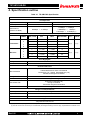
Table 8.1 Parameterization Table
Parameter Name
Values
P_FPGA_TYPE
0,1
P_LANE_NUM
1,2,4,8
P_BYTE_MD
3,4,5
Description
FPGA select
0:Virtex-6,
1:Spartan-6
Number of high-speed serial Data Lanes
Byte width of the video data
P_PLL_DIVSEL_xxx
(1)
PLL settings of the GTX/GTP transceivers
P_PXCLK_xxx
(2)
Settings of the PLL that generates the internal clock from the
pixel clock
P_GTPCLKOUT_xxx
(3)
Settings of the PLL that generates the internal clock from the
GTPCLKOUT port of the GTX/GTP transceivers
(1),(2),(3) Refer to the TIP-VBY1-TX/RX User Manual and GTX/GTP transceivers User Guide for the details of these parameters.
9. Verification
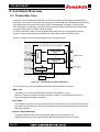
The TIP-VBY1HS Core has been verified with the RTL simulation and hardware validation of
connectivity test by THine Electronics, Inc.
9.1. Simulation
A highly-parameterizable command-based test bench was used to test the core.
All byte-modes and data lane numbers are tested by following construcition.
9.2. Hardware Validation
The TIP-VBY1HS Core has been validated using CVK kit of Tokyo Electron Device Ltd.(TED).
The hardware has been tested against the V-by-One® HS evaluation board from THine
electronics, Inc. for warranty of the connectibity.
Rev1.00
13