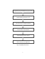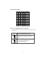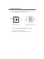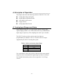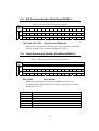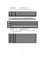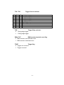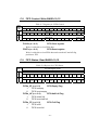
1
Copyright The documentation and the software included with this product are copyrighted 2003 by Advantech Co., Ltd. All rights are reserved. Advantech Co., Ltd. reserves the right to make improvements in the products described in this manual at any time without notice. No part of this manual may be reproduced, copied, translated or transmitted in any form or by any means without the prior written permission of Advantech Co., Ltd. Information provided in this manual is intended to be accurate and reliable. However, Advantech Co., Ltd. assumes no responsibility for its use, nor for any infringements of the rights of third parties, which may result from its use. Acknowledgments PC-LabCard is a trademark of Advantech Co., Ltd. IBM and PC are trademarks of International Business Machines Corporation. MS-DOS, Windows, Microsoft Visual C++ and Visual BASIC are trademarks of Microsoft Corporation. Intel and Pentium are trademarks of Intel Corporation. Delphi and C++ Builder are trademarks of Inprise Corporation. CE notification The PCI-1714, developed by ADVANTECH CO., LTD., has passed the CE test for environmental specifications when shielded cables are used for external wiring. We recommend the use of shielded cables. This kind of cable is available from Advantech. Please contact your local supplier for ordering information. On-line Technical Support For technical support and service, please visit our support website at: http://www.advantech.com/support Part No. 2003171400 Printed in Taiwan -i- 1st Edition July 2003 (This page is left blank for hard printing.) - ii - Contents 1. INTRODUCTION.................................................................................................................. 1 1.1 FEATURES ........................................................................................................................ 1 1.2 APPLICATIONS .................................................................................................................. 3 1.3 INSTALLATION GUIDE ....................................................................................................... 3 1.4 SOFTWARE OVERVIEW ..................................................................................................... 5 1.5 DEVICE DRIVERS PROGRAMMING ROADMAP ................................................................... 6 1.6 ACCESSORIES ................................................................................................................... 8 2. INSTALLATION.................................................................................................................... 9 2.1 UNPACKING ...................................................................................................................... 9 2.2 DRIVER INSTALLATION ................................................................................................... 11 2.3 HARDWARE INSTALLATION ............................................................................................ 13 2.4 DEVICE SETUP & CONFIGURATION ................................................................................. 16 2.5 DEVICE TESTING ........................................................................................................... 19 3. SIGNAL CONNECTIONS .................................................................................................. 21 3.1 OVERVIEW ..................................................................................................................... 21 3.2 SWITCH AND JUMPER SETTINGS ..................................................................................... 21 3.3 SIGNAL CONNECTIONS ................................................................................................... 24 3.3 SIGNAL CONNECTIONS ................................................................................................... 24 4. PRINCIPLES OF OPERATION ........................................................................................ 25 4.1 ANALOG INPUT RANGES AND GAINS............................................................................. 25 4.2 ANALOG INPUT ACQUISITION MODES ........................................................................... 26 4.3 A/D SAMPLE CLOCK SOURCES ..................................................................................... 31 4.4 TRIGGER SOURCES ........................................................................................................ 33 4.5 ANALOG INPUT DATA FORMAT ...................................................................................... 35 5. CALIBRATION ................................................................................................................... 36 APPENDIX A. SPECIFICATIONS ........................................................................................ 45 APPENDIX B. BLOCK DIAGRAM ...................................................................................... 47 - iii - APPENDIX C. REGISTER STRUCTURE AND FORMAT................................................ 49 C.1 OVERVIEW ..................................................................................................................... 49 C.2 REGISTER FORMAT......................................................................................................... 49 C.3 A/D SINGLE VALUE ACQUISITION- WRITE BASE+0, 2, 4, 6........................................ 54 C.4 AI RANGE CONTROL- WRITE/READ BASE+8............................................................... 55 C.5 A/D CONVERTER ENABLE- WRITE/READ BASE+A ...................................................... 56 C.6 CLOCK SOURCE AND DIVIDER- WRITE/READ BASE+C ................................................ 56 C.7 TRIGGER MODE AND SOURCE- WRITE/READ BASE+E................................................. 57 C.8 FIFO CONTROL- WRITE BASE+10,12 .......................................................................... 59 C.9 FIFO STATUS- READ BASE+10,12 ............................................................................... 59 C.10 FIFO FOR PROGRAMMABLE FLAG- WRITE/READ BASE+14,16,18,1A .................... 60 C.11 DMA COUNTER- WRITE/READ BASE+1C, WRITE BASE+1E ................................. 61 C.12 INTERRUPT CONTROL/FLAG- WRITE/READ BASE+20................................................ 62 C.13 CLEAR INTERRUPT- WRITE BASE+22......................................................................... 63 C.14 ANALOG TRIGGER THRESHOLD VOLTAGE- WRITE/READ BASE+24 ........................ 64 C.15 CALIBRATION COMMAND- WRITE/READ BASE+28.................................................... 65 C.16 BOARD ID- READ BASE+2C ...................................................................................... 66 C.17 RESET DMA START CHANNEL TO CH0- WRITE BASE+30.......................................... 66 C.18 AD CHANNEL N DATA- READ BASE+30,32 .............................................................. 66 C.19 DMA REQUEST SELECTOR- WRITE BASE+34 ............................................................ 68 - iv - 1. Introduction ____________________________ Thank you for buying the Advantech PCI-1714. The PCI-1714 is a 30MHz Simultaneous 4-CH Analog Input Card for the PCI bus. It is an advanced-performance data acquisition card based on 32-bit PCI Bus architecture. The maximum sampling rate of PCI-1714 is up to 30MHz samples per second, with an emphasis on continuous, non-stop, high-speed, streaming data of A/D samples to host memory. The following sections of this chapter will provide further information about features of the multifunction cards, a Quick Start for installation, together with some brief information on software and accessories for the PCI-1714 card. 1.1 Features The Advantech PCI-1714 offers the following main features: 32-bit PCI-Bus Mastering DMA data transfer 4 A/D converters simultaneously sampling 12-bit A/D converter up to 30M samples per second 4 single-ended analog input channels Programmable gain for each input channel On board FIFO memory Multiple A/D triggering modes Programmable pacer/counter Auto calibration Some of them are highlighted and more detailed as following. PCI-Bus Mastering Data Transfer The PCI-1714 supports PCI-Bus mastering DMA for high-speed data transfer. By setting aside a block of memory in the PC, the PCI-1714 performs bus-mastering data transfers without CPU intervention, freeing the CPU to perform other more urgent tasks such as data analysis and graphic manipulation. The function allows users to run -1- all I/O functions simultaneously at full speed without losing data. Simultaneous Sampling The PCI-1714 capable of simultaneous sampling uses 4 identical circuitries and ADC for each analog input channel. Where the time relationship between inputs is important, this feature let you sample simultaneously. Supports S/W, Internal and External Pacer Triggering The PCI-1714 supports three kinds of trigger modes for A/D conversion: software triggering, internal pacer triggering and external pacer triggering. The software trigger allows users to acquire a sample when it is needed; the internal pacer triggers continuously high-speed data acquisition. The PCI-1714 also accepts external trigger sources, allowing synchronous sampling with external devices. On-board FIFO Memory There are 32K samples of FIFO memory on PCI-1714. This is an important feature for faster data transfer and more predictable performance under Windows system. Auto Calibration PCI-1714 features software auto calibration. There is no variable resister trimming required. This is convenient for user to calibrate. Note: ✎ For detailed specifications of the PCI-1714, please refer to Appendix A, Specifications. -2- 1.2 Applications The following are some of the possible applications of PCI-1714: Testing Instrument 1.3 Ultrasound Imaging Gamma Camera Imaging CCD Camera Imaging Video Digitizing Installation Guide Before you install your PCI-1714 card, please make sure you have all the following necessary components: PCI-1714 DA&C card PCI-1714 User’s Manual This manual Driver software Advantech DLL drivers (included in the companion CD-ROM) Wiring cable PCL-10901-1, BNC-BNC (optional) Wiring board ADAM-3909 (optional) Computer Personal computer or workstation with a PCI-bus slot (running Windows 2000/95/98/ ME/NT/XP) Some other optional components are also available for enhanced operation: Application software ActiveDAQ, GeniDAQ or other third-party software packages After you get the necessary components and maybe some of the accessories for enhanced operation of your Multifunction card, you can then begin the Installation procedures. Figure 1-1 on the next page provides a concise flow chart to give users a broad picture of the software and hardware installation procedures: -3- Install Driver from CD-ROM, then power-off PC Install Hardware and power-on PC Use driver utility to configure hardware Use test utility to test hardware Read examples & driver manual Start to write your own application Fig. 1-1 Installation Flow Chart -4- 1.4 Software Overview Advantech offers a rich set of DLL drivers, third-party driver supports and application software to help fully utilize the functions of your PCI-1714 card: Device Drivers (on the companion CD-ROM) LabVIEW driver Advantech ActiveDAQ Advantech GeniDAQ Programming choices for DA&C cards You may use Advantech application software such as Advantech Device Drivers. On the other hand, advanced users can use another option for register-level programming, although it is not recommended due to its laborious and time-consuming nature. Device Drivers The Advantech Device Drivers software is included on the companion CD-ROM at no extra charge. It also comes with all Advantech DA&C cards. Advantech’s device drivers feature a complete I/O function library to help boost your application performance. The Advantech Device Drivers for Windows 2000/95/98/ME/NT/XP works seamlessly with development tools such as Visual C++, Visual Basic, Inprise C++ Builder and Inprise Delphi. Register-level Programming Register-level programming is reserved for experienced programmers who find it necessary to write code directly at the level of device registers. Since register-level programming requires much effort and time, we recommend that you use the Advantech Device Drivers instead. However, if register-level programming is necessary, you should refer to the relevant information in Appendix C, Register Structure and Format, or to the example codes included on the companion CD-ROM. -5- 1.5 Device Drivers Programming Roadmap This section will provide you a roadmap to demonstrate how to build an application from scratch using Advantech Device Drivers with your favorite development tools such as Visual C++, Visual Basic, Delphi and C++ Builder. The step-by-step instructions on how to build your own applications using each development tool will be given in the Device Drivers Manual. Moreover, a rich set of example source code is also given for your reference. Programming Tools Programmers can develop application programs with their favorite development tools: ❏ Visual C++ ❏ Visual Basic ❏ Delphi ❏ C++ Builder For instructions on how to begin programming works in each development tool, Advantech offers a Tutorial Chapter in the Device Drivers Manual for your reference. Please refer to the corresponding sections in this chapter of the Device Drivers Manual to begin your programming efforts. You can also look at the example source code provided for each programming tool, since they can get you very well oriented. The Device Drivers Manual can be found on the companion CD-ROM. Or if you have already installed the Device Drivers on your system, The Device Drivers Manual can be readily accessed through the Start button: Start/Programs/Advantech Driver V2.1/Device Driver Manual The example source codes could be found under the corresponding installation folder such as the default installation path: -6- \Program Files\Advantech\ADSAPI\Examples For information about using other function groups or other development tools, please refer to the Creating Windows 95/NT/2000 Application with Device Drivers chapter and the Function Overview chapter on the Device Drivers Manual. Programming with Device Drivers Function Library Advantech Device Drivers offers a rich function library to be utilized in various application programs. This function library consists of numerous APIs that support many development tools, such as Visual C++, Visual Basic, Delphi and C++ Builder. According to their specific functions or services, those APIs can be categorized into several function groups: Device Function Analog Input/Output Function Digital Input/Output Function Port I/O Function Counter Function Temperature Measurement Function Temperature measurement Function Alarm Function Communication port Function High speed Function Hardware Function For the usage and parameters of each function, please refer to the Function Overview chapter in the Device Drivers Manual. Troubleshooting Device Drivers Error Driver functions will return a status code when they are called to perform a certain task for the application. When a function returns a code that is not zero, it means the function has failed to perform its designated function. To troubleshoot the Device Drivers error, you -7- can pass the error code to DRV_GetErrorMessage function to return the error message. Or you can refer to the Device Drivers Error Codes Appendix in the Device Drivers Manual for a detailed listing of the Error Code, Error ID and the Error Message. 1.6 Accessories Advantech offers a complete set of accessory products to support the PCI-1714 card. These accessories include: Wiring Cable PCL-10901-1 The PCL-10901-1 cable is specially designed for PCI-1714 cards to connect to the wiring board, ADAM-3909, for external synchronization signal source, such like an external trigger and/or clock signal. Source Signal Cable The source signal cable is designed as BNC-BNC or BNC for one side and open-end for the other. The cable links the PCI-1714 cards with the signal source via the BNC connector. There are all four BNC ports on board available for simultaneous signal input. Wiring Boards ❏ ADAM-3909 The ADAM-3909 is a DB-9 Wiring Terminal for DIN-rail Mounting. This terminal module can be readily connected to the Advantech PC-Lab cards and allows easy yet reliable access to individual pin connections for the PCI-1714 card. -8- 2. Installation _____________________________ This chapter gives users a package item checklist, proper instructions about unpacking and step-by-step procedures for both driver and card installation. 2.1 Unpacking After receiving your PCI-1714 package, please inspect its contents first. The package should contain the following items: ; PCI-1714 card ; Companion CD-ROM (DLL driver included) ; User’s Manual The PCI-1714 card harbors certain electronic components vulnerable to electrostatic discharge (ESD). ESD could easily damage the integrated circuits and certain components if preventive measures are not carefully paid attention to. Before removing the card from the antistatic plastic bag, you should take following precautions to ward off possible ESD damage: Touch the metal part of your computer chassis with your hand to discharge static electricity accumulated on your body. Or use a grounding strap. Touch the anti-static bag to a metal part of your computer chassis before opening the bag. Take hold of the card only by the metal bracket when removing it from the bag. After taking out the card, first you should: Inspect the card for any possible signs of external damage (loose or damaged components, etc.). If the card is visibly damaged, please notify our service department or the local sales representative immediately. Avoid installing a damaged card into your system. -9- Also, pay extra caution to the following aspects to ensure proper installation: a Avoid physical contact with materials that could hold static electricity such as plastic, vinyl and Styrofoam. a Whenever you handle the card, grasp it only by its edges. DO NOT TOUCH the exposed metal pins of the connector or the electronic components. Note: ✎ Keep the anti-static bag for future use. You might need the original bag to store the card if you have to remove the card from the PC or transport it elsewhere. - 10 - 2.2 Driver Installation We recommend you to install the driver before you install the PCI-1714 card into your system, since this will guarantee a smooth installation process. The Advantech Device Drivers Setup program for the PCI-1714 card is included on the companion CD-ROM that is shipped with your DA&C card package. Please follow the steps below to install the driver software: Step 1: Insert the companion CD-ROM into your CD-ROM drive. Step 2: The Setup program will be launched automatically if you have the autoplay function enabled on your system. When the Setup Program is launched, you’ll see the following Setup Screen. Note: ✎ If the autoplay function is not enabled on your computer, use Windows Explorer or the Windows Run command to execute SETUP.EXE on the companion CD-ROM. - 11 - Fig. 2-1 The Setup Screen of Advantech Automation Software Step 3: Select the Individual Drivers option. Step 4: Select the specific device then just follow the installation instructions step by step to complete your device driver setup. Fig. 2-2 Different options for Driver Setup For further information on driver-related issues, an online version of Device Drivers Manual is available by accessing the following path: Start/Programs/Advantech Device Drivers V2.1/Device Driver Manual - 12 - 2.3 Hardware Installation After the DLL driver installation is completed, you can now go on to install the PCI-1714 card in any PCI slot on your computer. But it is suggested that you should refer to the computer user manual or related documentation if you have any doubt. Please follow the steps below to install the card on your system. Note: ✎ Make sure you have installed the driver first before you install the card (please refer to 2.2 Driver Installation) Step 1: Turn off your computer and unplug the power cord and cables. TURN OFF your computer before installing or removing any components on the computer. Step 2: Remove the cover of your computer. Step 3: Remove the slot cover on the back panel of your computer. Step 4: Touch the metal part on the surface of your computer to neutralize the static electricity that might be on your body. Step 5: Insert the PCI-1714 card into a PCI slot. Hold the card only by its edges and carefully align it with the slot. Insert the card firmly into place. Use of excessive force must be avoided, otherwise the card might be damaged. Step 6: Fasten the bracket of the PCI-1714 card on the back panel rail of the computer with screws. Step 7: Connect appropriate accessories (such as source /sync signal cables, wiring terminals, etc. if necessary) to the PCI-1714 card. Step 8: Replace the cover of your computer chassis. Re-connect the cables you removed in Step 2. Step 9: Plug in the power cord and turn on the computer. Note: ✎ In case you installed the card without installing the DLL driver first, Windows 95/98/ME will recognize your card as an “unknown device” after rebooting, and will prompt you to provide the necessary driver. You - 13 - should ignore the prompting messages (just click the Cancel button) and set up the driver according to the steps described in 2.2 Driver Installation. After the PCI-1714 card is installed, you can verify whether it is properly installed on your system in the Device Manager: 1. Access the Device Manager through Control Panel/System/Device Manager. 2. The device name of the PCI-1714 should be listed on the Device Manager tab on the System Property Page. Fig. 2-3 The device name listed in the Device Manager Note: ✎ If your card is properly installed, you should see the device name of your card listed on the Device Manager tab. If you do see your device name listed on it but marked with an exclamation sign “!”, it means your card has not been correctly installed. In this case, - 14 - remove the card device from the Device Manager by selecting its device name and press the Remove button. Then go through the driver installation process again. After your card is properly installed on your system, you can now configure your device using the PCI-1714 Utility program that has itself already been installed on your system during driver setup. A complete device installation procedure should include board selection and device setup. After that, you can operate this card through the operation. The following sections will guide you through the board selection, device setup and operation of your device. - 15 - 2.4 Device Setup & Configuration The PCI-1714 Utility Program is a utility that allows you to setup, configure and test your device, and later store your settings on the system registry. These settings will be used when you call the APIs of Advantech Device Drivers. Setting Up the Device Step 1: To install the I/O device for your card, you must first run the Device Manager program (by accessing Start/Programs/ Advantech Device Drivers V2.1). Step 2: You can then view the device(s) already installed on your system (if any) in the Installed Devices list box. Since you haven’t installed any device yet, you might see a blank list such as the one below (Fig. 2-4). Fig. 2-4 The Device Manager dialog box - 16 - Step 3: Scroll down the Supported Devices box to find the device that you wish to install, then click the Add… button to evoke the Existing unconfigured PCI-1714 dialog box such as one shown in Fig. 2-5. The Existing unconfigured PCI-1714 dialog box lists all the installed devices on your system. Select the device you want to configure from the list box and press the OK button. Fig. 2-5 The “Device(s) Found” dialog box Step 4: After you have finished configuring the device, click OK and the device name will appear in the Installed Devices box as the following: - 17 - Fig. 2-6 The Device Name appearing on the list of devices box Note: ✎ As we have noted, the device name “001:<PCI-1714 BoardID=7 I/O=c800H>” begins with a device number “000”, which is specifically assigned to each card. The device number is passed to the driver to specify which device you wish to control. If you want to test the card device further, go right to the next section on the Device Testing. - 18 - 2.5 Device Testing Following through the Setup and Configuration procedures to the last step described in the previous section, you can now proceed to test the device by clicking the Test button on the I/O Device Installation dialog box (Fig. 2-7). A Device Test dialog box will appear accordingly: Fig. 2-7 The Device Test dialog box of PCI-1714 On the Device Test dialog box, users are free to test various functions of PCI-1714 on the Analog input tabs, functions on the other tabs are not supported at this stage. Note: ✎ You can access the Device Test dialog box either by the previous procedure for the Device Installation Program or simply by accessing Start/Programs/Advantech Driver for 95 and 98 (or for NT) /Test Utility. - 19 - Testing Analog Input Function Click the Analog Input tab to bring it up to front of the screen. Select the input range for each channel in the Input range drop-down boxes. Configure the sampling rate on the scroll bar. Switch the channels by using the up/down arrow. Fig. 2-8 Analog Input tab on the Device Test dialog box - 20 - 3. Signal Connections ______________________ Maintaining proper signal connections is one of the most important factors to ensure that your application system is sending and receiving data correctly. A good signal connection can avoid unnecessary and costly damage to your PC and other hardware devices. This chapter provides useful information about how to connect input and output signals to the PCI-1714 via the I/O connector. 3.1 Overview Maintaining signal connections is one of the most important factors in ensuring that your application system is sending and receiving data correctly. A good signal connection can avoid unnecessary and costly damage to your PC and other hardware devices. This chapter provides useful information about how to connect input and output signals to the PCI-1714 via the I/O connector. 3.2 Switch and Jumper Settings The PCI-1714 card has one function switch and five jumper settings. Fig. 3-1 Card connector, jumper and switch locations - 21 - Board ID setting (SW1) ID3 1 1 1 1 1 1 1 1 0 0 0 0 0 0 0 0 ID2 1 1 1 1 0 0 0 0 1 1 1 1 0 0 0 0 ID1 1 1 0 0 1 1 0 0 1 1 0 0 1 1 0 0 ID0 1 0 1 0 1 0 1 0 1 0 1 0 1 0 1 0 Board ID 0 1 2 3 4 5 6 7 8 9 10 11 12 13 14 15 Note: On: 1, Off: 0 Power on configuration after hot reset (JP1) To see the table below, User can use the JP1 to set the hot reset type of PCI-1714. JP1 Power on configuration after hot reset Keep the I/O configuration while hot reset. Clear the I/O configuration to default while hot reset. - 22 - Input terminator select (JP2 to JP5) To see the table below, User can use the JP2 to JP5 to set input terminator value for each AI channel CH0 to CH3, respectively. JP2, JP3, JP4, JP5 Input terminator select 50Ω 1MΩ High impedance - 23 - 3.3 Signal Connections CN1 Pin Assignment Figure 3-2 shows the pin assignments for the PS-2 connector on the PCI-1714 and the DB-9 connector on the cable. GND EXT TRIG0 1 NC 2 4 EXT TRIG0 NC 6 1 EXT CLK1 EXT CLK0+ 3 GND 4 2 5 3 EXT CLK0- EXT CLK0- 5 9 GND 8 GND 7 GND 6 EXT CLK1 EXT CLK0+ On board PS-2 connector PS2 To DB-9 Cable Connector Fig. 3-2 I/O connector pin assignment for the PCI-1714 J1 to J4 BNC are the AI input connectors. J1 is for AI0, J2 is for AI1, J3 is for AI2 and J4 is for AI3. - 24 - 4. Principles of Operation ___________________ This chapter describes the following features of the PCI-1714 card: Analog input ranges and gains Analog input acquisition modes A/D sample clock sources Trigger sources Analog Input Data Format 4.1 Analog Input Ranges and Gains Each channel on the PCI-1714 can measure bipolar analog input signals ranging within ± 10 V FSR, and can be set up with different input ranges respectively. The sampling rate can be up to 30 MS/s. The PCI-1714 also provides various gain levels that are programmable per channel. Table 4-1 lists the effective ranges supported by the PCI-1714 using these gains. Table 4-1 Gains and Analog Input Range Gain Analog Input Range 1 2 5 10 ±5 V ±2.5 V ±1 V ±0.5 V For each channel, choose the gain level that provides most optimal range that can accommodate the signal range you have to measure. For detailed information, please refer to Appendix C.4 AI Range Control. - 25 - 4.2 Analog Input Acquisition Modes The PCI-1714 can acquire data in single value, pacer, post-trigger, delay-trigger, about-trigger and pre-trigger acquisition modes. These analog input acquisition modes are described in more details in the following: Single Value Acquisition Mode The single value acquisition mode is the simplest way to acquire data. Once the software issues a trigger command, the A/D converter will convert one data, and return it immediately. User can check the A/D FIFO status (Read BASE+10, 12) to make sure if the data is ready to be received. For detailed information, please refer to Appendix C.8 FIFO Control, Appendix C.9 FIFO Status, Appendix C.10 FIFO for Progarmmable Flag. Pacer Acquisition Mode Use pacer acquisition mode to acquire data if you want to accurately control the time interval between conversions of individual channels in a scan. A/D conversion clock comes from A/D counter or external clock source on connector. A/D conversion starts when the first clock signal comes in, and will not stop if the clock is still continuously sending into it. Conversion data is put into the A/D FIFO. For high-speed data acquisition, you have to use the DMA data transfer for analog input to prevent data loss. Post-Trigger Acquisition Mode Post-trigger allows you to acquire data based on a trigger event. Posttrigger acquisition starts when the PCI-1714 detects the trigger event and stops when the preset number of post-trigger samples has been acquired or when you stop the operation. This trigger mode must work with the DMA data transfer mode enabled. Use post-trigger acquisition mode when you want to acquire data when a post-trigger event occurs. Please specify the following parameters when using software in post-trigger acquisition mode: - 26 - Set to Post-Trigger Acquisition Mode The A/D sample clock source and sampling rate The trigger source The acquired sample number N Fig. 4-1 Post-Trigger Acquisition Mode Delay Trigger Acquisition Mode In delay trigger mode, data acquisition will be activated after a preset delay number of sample has been taken after the trigger event. The delay number of sample ranges from 2 to 65535 as defined in DMA counter. Delay-trigger acquisition starts when the PCI-1714 detects the trigger event and stops when the specified number of A/D samples has been acquired or when you stop the operation. This triggering mode must work with the DMA data transfer mode enabled Please specify the following parameters when using software in delay trigger mode: Set to Delay-Trigger Acquisition Mode The sample clock source and sampling rate The trigger source The acquired sample number N The sample number M delays after the delay-trigger event happened - 27 - Fig. 4-2 Delay-Trigger Acquisition Mode About Trigger Acquisition Mode Use about-trigger acquisition mode when you want to acquire data both before and after a specific trigger event occurs. This operation is equivalent to doing both a pre-trigger and a post-trigger acquisition. When using software, please specify the following parameters, when using software in About-Trigger acquisition mode: Set to About-Trigger Acquisition Mode The sample clock source and sample rate The trigger source The total acquired sample number N The specific sample number M before the trigger event. The range of preset sample number is from 2 to 65536 samples. In about-trigger mode, users must first designate the size of the allocated memory and the amount of samples to be snatched after the trigger event happens. The about-trigger acquisition starts when the first clock signal comes in. Once a trigger event happens, the on-going data acquisition will continue until the designated amount of samples have been reached. When the PCI-1714 detects the selected about trigger event, the card keeps acquiring the preset number of samples, and kept the total number of samples on the FIFO. - 28 - Fig. 4-3 About-Trigger Acquisition Mode - 29 - Pre-Trigger Acquisition Mode Pre-Trigger mode is a particular application of about-trigger mode. Use pre-trigger acquisition mode when you want to acquire data before a specific trigger event occurs. Pre-trigger acquisition starts when you start the operation and stops when the trigger event happens. Then the specific number of samples will be reversed in the FIFO before the pre-trigger event occurred. Please specify the following parameters, when using software in Pre-trigger acquisition mode: Set to Pre-Trigger Acquisition Mode The sample clock source and sample rate The trigger source Assume the total acquired sample number is N, then set the total sample number to be N+2. Fig. 4-4 Pre-Trigger Acquisition Mode - 30 - 4.3 A/D Sample Clock Sources The PCI-1714 can adopt both internal and external clock sources for pacer, post-trigger, delay-trigger, about-trigger acquisition modes: Internal A/D sample clock with 8-bit Counter External A/D sample clock that is connected to either the EXT-CLK0 (the differential clock source) or the EXT_CLK1 (the single ended clock source) on the ADAM-3909 screw terminal board. The internal and both external A/D sample clocks are described in more details as the following. Internal A/D Sample Clock The internal A/D sample clock uses a 60 MHz time base. Conversions start on the rising edge of the counter output. You can use software to specify the clock source as internal and the sampling frequency to pace the operation. The minimum frequency is 234375 S/s, the maximum frequency is 30 MS/s. According to the sampling theory (Nyquist Theorem), you must specify a frequency that is at least twice as fast as the input’s highest frequency component to achieve a valid sampling. For example, to accurately sample a 300 kHz signal, you have to specify sampling frequency of at least 600 kHz. This consideration can avoid an error condition often know as aliasing, in which high frequency input components appear erroneously as lower frequencies when sampling. External A/D Sample Clock 0 The external sample clock 0 is a sine wave signal source which is converted to a TTL signal inside the PCI-1714. This signal is AC coupled. The input impedance of external clock 0 is 50 ohms and the input level is 2 volts peak-to-peak. Please note that the frequency of the external clock is the system clock. The maximum A/D clock frequency is half of the system clock. - 31 - External A/D Sample Clock 1 The external sample clock 1 is a digital clock. The input impedance is 50 ohms and the input level should be 2.4V~5V into the 50-ohm load. This signal is DC coupled. 60 Mhz Trigger and Control Logic 8-bit Counter A/D Converter Internal EXT_CLK 0 Trigger Source EXT_CLK 1 Fig 4-5 PCI-1714 Sample Clock Sources - 32 - 4.4 Trigger Sources The PCI-1714 supports the following trigger sources for post-, delay-, about- and pre-trigger acquisition modes: Software trigger, External digital (TTL) trigger, and Analog threshold trigger. With PCI-1714, user can define the type of trigger source as rising-edge or falling-edge. These following sections describe these trigger sources in more detail. Software Trigger A software trigger event occurs when you start the analog input operation (the computer issues a write to the board to begin acquisitions). When you write the value to analog input trigger flag TRGF on Write BASE+Eh to produce either a rising-edge or falling-edge trigger, depending upon the trigger source type you choose. This edge will then act as an A/D trigger event. For detailed information, please refer to Appendix C.7 Trigger Mode and Source. External Digital (TTL) Trigger For analog input operations, an external digital trigger event occurs when the PCI-1714 detects either a rising or falling edge on the External A/D TTL trigger input signal from screw terminal EXT_TRIG on the ADAM-3909 screw terminal board. The trigger signal is TTL-compatible. Analog Threshold Trigger For analog input operations, an analog trigger event occurs when the PCI-1714 detects a transition from above a threshold level to below a threshold level (falling edge), or a transition from below a threshold level to above a threshold level (rising edge). User should connect the analog signals from the external device to one of the four BNC source connectors. Which one of the four sources is selected as the trigger source can be defined or identified by writing to or reading from the - 33 - flags from TS0 to TS2 of Write/Read BASE+Eh. On the PCI-1714, the analog trigger threshold voltage level is set using a dedicated 8-bit DAC; you can write or read the flags from AT0 to AT7 on Write/Read BASE+24h to define or identify the analog trigger threshold voltage level. Please also refer to the Appendix C.14 Analog Trigger Threshold Voltage for more details. - 34 - 4.5 Analog Input Data Format Table 4-2 Analog Input Data Format A/D Code Hex. Dec. 000h 0d 7FFh 2047d 800h 2048d FFFh 2095d 1LSB Mapping Voltage -FS -1 LSB 0 FS-1 LSB FS/2048 Table 4-3 The corresponding Full Scale values for various Input Voltage Ranges Gain 1 2 5 10 Range ±5 ±2.5 ±1 ±0.5 - 35 - FS 5 2.5 1 0.5 (This page is left blank for hard printing.) - 36 - 5. Calibration _____________________________ This chapter offers you a brief guide to the calibration procedure. The PCI-1714 has been well calibrated at the factory for initial use. Users are not necessary to calibrate the PCI-1714 in normal conditions. However, if some other conditions that the users have to calibrate the PCI-1714, then they can follow the procedure listed below to perform the necessary calibration. To perform an effective calibration, the user has to prepare a standard 4-1/2 digits resolution, stable and low-noise DC voltage source. It is important that the accuracy of the device will depend on the accuracy of the DC source. Calibration Procedure Step 1: Click the Setup button on the Advantech Device Manager window (Fig.5-1) to launch the PCI-1714 Device Setting window (Fig.5-2). Fig.5-1 Click the Setup button to launch the Device Setting - 37 - Step 2: Select the input range of the channel which you want to calibrate. Step 3: Click the Calibration button to start the calibration process. The Calibration Wizard window will pop up. Note: ✎ Each calibration process can calibrate only one channel and one input range at a time. Fig.5-2 Click the Calibration button to launch the calibration - 38 - Step 4: Follow the instruction of Calibration Wizard to input a correct DC voltage as a reference and click the Next button to proceed to the next step. This wizard will help you calibrate your PCI-1714 device Fig.5-3 The start-up window of offset calibration Step 5: Click the Start button to start the Offset Calibration. Note that the Status will indicate Unknown as default at the beginning. Fig.5-4 The adjustment process of offset calibration - 39 - Step 6: If the reference DC voltage source and the wiring are both correct, the calibration will proceed automatically after the Start button is clicked. When the offset calibration is completed, the Status will indicate Succeeded, then click the Next button to proceed to the next step Fig.5-5 Offset calibration succeeded Step 6a: Once the Status indicates Failed, please check if both the wiring and the input voltage are correct. When finished checking, click the Start button again to restart the procedure, or click the Cancel button to stop the calibration. Adjust Offset Value Fig.5-6 Offset calibration failed - 40 - Step 7: If the offset calibration is completed, then it is going to proceed to the Gain Calibration. The steps of gain calibration are quite similar to those of the offset calibration. Follow the instructions of the Calibration Wizard to input a correct DC voltage and click the Next button to proceed., Fig.5-7 The start-up window of offset calibration Step 8: Click the Start button to start gain calibration. Note that the Status will indicate Unknown as default at the beginning. Fig.5-8 The adjustment process of gain calibration - 41 - Step 9: When the gain calibration is completed then click the Next button to proceed. Fig.5-9 Gain calibration succeeded Step 9a: Once the Status indicates Failed, please check if both the wiring and the input voltage are correct. When finished checking, click the Start button again to restart the procedure, or click the Cancel button to stop the calibration. Fig.5-10 Gain calibration failed - 42 - Step 10: When the current channel is calibrated, click the Finish button to end the procedure. You can proceed to Step 3 to select another channel for calibration, and repeat from Step 4 to Step 9, until the rest of the channels are all calibrated one after one. Fig.5-11 Calibration procedure completed - 43 - (This page is left blank for hard printing.) - 44 - Appendix A. Specifications _________________ Analog Input: Channels 4 single-ended analog input channels Resolution 12-bit FIFO Size 32K locations Max. Sampling Up to 30MHz1 Rate1 Conversion 500 ns Common mode ±11 V max. Time voltage (operational) Input range and Gain List Gain 1 2 5 10 Range ±5V ±2.5V ±1V ±0.5V Gain 1 2 5 10 Zero (μV/ ±30 ±30 ±30 ±30 Drift ℃) Gain (ppm// ±30 ±30 ±30 ±30 ℃) Gain 1 2 5 10 Small Signal Bandwidth for Bandwi 7MHz 7MHz 7MHz 7MHz dth PGA (-3dB) Max. Input Input Surge ±15 V 30 Vp-p voltage Protect 50Ω/1MΩ/∞ jumper selectable 100pF Input Impedance Software, pacer, post-trigger, pre-trigger, Trigger Mode delay-trigger, about-trigger DNLE: ±1LSB (No Missing Codes:12 Bits Guaranteed) INLE: ±2LSB DC Offset Adjustable to ±1LSB Accuracy error Gain error Adjustable to ±1LSB SINAD: S/(N+D): 68 dB AC ENOB: 11bits THD: -75 dB Logic level Low: 0.8 V max. High: 2.0V min. Input External TTL 50 ohms impedance Trigger Input Input DC coupled Logic level 5.0V peak to peak External sin Input 50 ohms wave Trigger impedance Input Input AC coupled External Analog Range By analog input range Trigger Input Resolution 8-bit 1 30 MHz is only for FIFO depth (32K). Continuous acquisition depends on platform performance. - 45 - General: I/O Connector Type Dimensions Power Consumption Temperature Relative Humidity Certification 4 BNC connector for AI 1 PS2 connector for ext. clock and trigger 137 mm x 107 mm (5.4" x 4.2") Typical +5 V @ 850 mA ; +12 V @ 600 mA Max. +5 V @ 1 A ; +12 V @ 700m A Operation 0~+70℃(32~158℉) Storage -20~+85℃(-4~185℉) 5~95%RH non-condensing (refer to IEC 68-2-3) CE certified - 46 - Appendix B. Block Diagram _________________ - 47 - (This page is left blank for hard printing.) - 48 - Appendix C. Register Structure and Format____ C.1 Overview The PCI-1714 is delivered with an easy-to-use 32-bit DLL driver for user programming under the Windows 2000/95/98/NT/ME/XP operating system. We advise users to program the PCI-1714 using the 32-bit DLL driver provided by Advantech to avoid the complexity of low-level programming by register. The most important consideration in programming the PCI-1714 at register level is to understand the function of the card's registers. The information in the following sections is provided only for users who would like to do their own low-level programming. C.2 Register format The register format is the basis to control the PCI-1714. There are some rules for programmer’s reference: 1. All registers are 32-bit format. Please use the DWORD command in your own software. 2. Some registers are used only for write or read. 3. Some registers can support write and read back, they usually use the same name. 4. Some registers could write any value to complete a command. 5. In general, read only register is called status register, write only register is called control register. 6. Some registers are very similar, usually denote as a group. For example, A4, A3, A2, A1, A0 usually denote as A4: A0. 7. In this document, 1Fh means hexadecimal number 1F. Table C-1 shows the function of each register of the PCI-1714 or driver and its address relative to the card's base address. - 49 - Table C-1 PCI-1714 register format (Part 1) Base Address + HEX PCI-1714 Register Format 15 14 13 12 11 10 9 8 7 6 5 4 3 2 1 0 AD4 AD3 AD2 AD1 AD0 AD4 AD3 AD2 AD1 AD0 AD4 AD3 AD2 AD1 AD0 AD4 AD3 AD2 AD1 AD0 AI Channel 0 Single Value Acquisition W 0h AI Channel 0 Data R TRG F OV G1 G0 AD11 AD10 AD9 AD8 AD7 AD6 AD5 AI Channel 1 Single Value Acquisition W 2h AI Channel 1 Data R TRG F OV G1 G0 AD11 AD10 AD9 AD8 AD7 AD6 AD5 AI Channel 2 Single Value Acquisition W 4h AI Channel 2 Data R TRG F OV G1 G0 AD11 AD10 AD9 AD8 AD7 AD6 AD5 AI Channel 3 Single Value Acquisition W 6h AI Channel 3 Data R TRG F OV G1 G0 AD11 AD10 AD9 AD8 AD7 AD6 AD5 AI Range Control Register W CH3_ CH3_ CH2_ CH2_ CH1_ CH1_ CH0_ CH0_ G1 G0 G1 G0 G1 G0 G1 G0 R CH3_ CH3_ CH2_ CH2_ CH1_ CH1_ CH0_ CH0_ G1 G0 G1 G0 G1 G0 G1 G0 8h A/D Converter Enable Register W Ah R CH3 CH2 CH1 CH0 CH3 CH2 CH1 CH0 Clock Source and Divider Register W CKS1 CKS0 DIV7 DIV6 DIV5 DIV4 DIV3 DIV2 DIV1 DIV0 Ch R CKS1 CKS0 DIV7 DIV6 DIV5 DIV4 DIV3 DIV2 DIV1 DIV0 Trigger Mode and Source Register W TRG DMA F _TCF TSE TS2 TS1 TS0 TM2 TM1 TM0 R TRG DMA F _TCF TSE TS2 TS1 TS0 TM2 TM1 TM0 Eh - 50 - Table C-1 PCI-1714 register format (Part 2) Base Address + HEX PCI-1714 Register Format 15 14 13 12 11 10 9 8 7 6 5 4 3 2 1 0 FIFO Control Register W FRST FCLR 1 1 10h FRST FCLR 0 0 FIFO Status Register R FIFO FIFO 1_AF 1_AE FIFO FIFO FIFO 0_FF 0_HF 0_EF FIFO FIFO 0_AF 0_AE FIFO FIFO FIFO 1_FF 1_HF 1_EF FIFO Control Register W FRST FCLR 3 3 12h FRST FCLR 2 2 FIFO Status Register R W 14h R W 16h R W 18h R W 1Ah R W 1Ch R W FIFO FIFO 3_AF 3_AE FIFO FIFO FIFO 3_FF 3_HF 3_EF FIFO FIFO 2_AF 2_AE FIFO FIFO FIFO 2_FF 2_HF 2_EF FIFO 0 Programmable Flag Register PF14 PF13 FP12 PF11 PF10 PF9 PF8 PF7 PF6 PF5 PF4 PF3 PF2 PF1 PF0 PF4 PF3 PF2 PF1 PF0 PF4 PF3 PF2 PF1 PF0 PF4 PF3 PF2 PF1 PF0 PF4 PF3 PF2 PF1 PF0 PF4 PF3 PF2 PF1 PF0 PF4 PF3 PF2 PF1 PF0 PF5 PF4 PF3 PF2 PF1 PF0 FIFO 0 Programmable Flag Register PF14 PF13 FP12 PF11 PF10 PF9 PF8 PF7 PF6 PF5 FIFO 1 Programmable Flag Register PF14 PF13 FP12 PF11 PF10 PF9 PF8 PF7 PF6 PF5 FIFO 1 Programmable Flag Register PF14 PF13 FP12 PF11 PF10 PF9 PF8 PF7 PF6 PF5 FIFO 2 Programmable Flag Register PF14 PF13 FP12 PF11 PF10 PF9 PF8 PF7 PF6 PF5 FIFO 2 Programmable Flag Register PF14 PF13 FP12 PF11 PF10 PF9 PF8 PF7 PF6 PF5 FIFO 3 Programmable Flag Register PF14 PF13 FP12 PF11 PF10 PF9 PF8 PF7 PF6 PF5 FIFO 3 Programmable Flag Register PF14 PF13 FP12 PF11 PF10 PF9 PF8 PF7 PF6 DMA Counter Register CN15 CN14 CN13 CN12 CN11 CN10 CN9 CN8 CN7 CN6 CN5 CN4 CN3 CN2 CN1 CN0 CN15 CN14 CN13 CN12 CN11 CN10 CN9 CN8 CN7 CN6 CN5 CN4 CN3 CN2 CN1 CN0 Rest DMA Counter 1Eh R - 51 - Table C-1 PCI-1714 register format (Part 3) Base Address + HEX PCI-1714 Register Format 15 14 13 12 11 10 9 8 7 6 5 4 3 2 1 0 Interrupt Control Register W INTE DMA FIFO FIFO FIFO FIFO FIFO FIFO FIFO FIFO _TC 3_AF 3_HF 2_AF 2_HF 1_AF 1_HF 0_AF 0_HF INTF INTF INTF INTF INTF INTF INTF INTF INTF INTF 8 7 6 5 4 3 2 1 0 20h R Clear Interrupt W 22h N/A R Analog Trigger Threshold voltage Register W AT7 24h R AT7 AT5 AT4 AT3 AT2 AT1 AT0 AT6 AT5 AT4 AT3 AT2 AT1 AT0 N/A W 26h N/A R W AT6 Analog Trigger Threshold voltage Register Calibration Command Register CG1 CG0 CG1 CG0 X CM2 CM1 CM0 CD7 CD6 CD5 CD4 CD3 CD2 CD1 CD0 CBU CM2 CM1 CM0 CD7 SY CD6 CD5 CD4 CD3 CD2 CD1 CD0 28h R W 2Ah R W Board ID 2Ch R BID3 BID2 BID1 BID0 W 2Eh R - 52 - Table C-1 PCI-1714 register format (Part 4) Base Address + HEX PCI-1714 Register Format 15 14 13 12 11 10 9 8 7 6 5 4 3 2 1 0 AD5 AD4 AD3 AD2 AD1 AD0 AD5 AD4 AD3 AD2 AD1 AD0 Reset start read channel to CH0 W 30h AD Channel n DATA R TRG F OV G1 G0 AD11 AD10 AD9 AD8 AD7 AD6 N/A W 32h AD Channel n+1 DATA R W TRG F OV G1 G0 AD11 AD10 AD9 AD8 AD7 AD6 DMA Request selector DS0 34h R - 53 - C.3 A/D Single Value AcquisitionWrite BASE+0, 2, 4, 6 In single value acquisition mode (SW trigger), the A/D converter will convert one sample when you write to the register Write BASE+0, 2, 4, 6 with any value. User can check the A/D FIFO status (FIFOn_FE) to make sure if the data is ready to be received. Table C-2 Register for Single Value Acquisition Base Address + HEX PCI-1714 Register Format 15 14 13 12 11 10 9 8 7 6 5 4 3 2 1 0 AD4 AD3 AD2 AD1 AD0 AD4 AD3 AD2 AD1 AD0 AD4 AD3 AD2 AD1 AD0 AD4 AD3 AD2 AD1 AD0 AI Channel 0 Single Value Acquisition W 0h AI Channel 0 Data R TRG F OV G1 G0 AD11 AD10 AD9 AD8 AD7 AD6 AD5 AI Channel 1 Single Value Acquisition W 2h AI Channel 1 Data R TRG F OV G1 G0 AD11 AD10 AD9 AD8 AD7 AD6 AD5 AI Channel 2 Single Value Acquisition W 4h AI Channel 2 Data R TRG F OV G1 G0 AD11 AD10 AD9 AD8 AD7 AD6 AD5 AI Channel 3 Single Value Acquisition W 6h AI Channel 3 Data R TRG F OV G1 G0 AD11 AD10 AD9 AD8 AD7 AD6 AD5 AD11: AD0 12 bits Data of A/D Conversion AD0 the least significant bit (LSB) of A/D data. AD11 the most significant bit (MSB) of A/D data. G1: G0 Range code These 2 bits indicate the input range of the data. G1 0 0 1 1 G0 0 1 0 1 Input range -5 to +5V -2.5 to +2.5V -1 to +1V -0.5 to +0.5V - 54 - OV Over range flag This bit indicates whether the input voltage is over range or not. Read 1 means over range. TRGF Trigger Flag (For about trigger use only) The trigger flag indicates whether a trigger event has happened during A/D conversion process. C.4 AI Range Control- Write/Read BASE+8 Table C-3 Register for Analog Input Range Control Base Address + HEX PCI-1714 Register Format 15 14 13 12 11 10 9 8 7 6 5 4 3 2 1 0 AI Range Control Register W CH3_ CH3_ CH2_ CH2_ CH1_ CH1_ CH0_ CH0_ G1 G0 G1 G0 G1 G0 G1 G0 R CH3_ CH3_ CH2_ CH2_ CH1_ CH1_ CH0_ CH0_ G1 G0 G1 G0 G1 G0 G1 G0 8h Analog Input Range Selector These registers are used to select the analog input range for each channel. CHn_G1 0 0 1 1 (n = 0~3) CHn_G0 0 1 0 1 Input range -5 to +5 V -2.5 to +2.5 V -1 to +1 V -0.5 to +0.5 V - 55 - C.5 A/D Converter Enable- Write/Read BASE+A Table C-4 Register for A/D Converter Enable Base Address + HEX PCI-1714 Register Format 15 14 13 12 11 10 9 8 7 6 5 4 3 2 1 0 CH3 CH2 CH1 CH0 CH3 CH2 CH1 CH0 A/D Converter Enable Register W Ah R CH3, CH2, CH1, CH0 A/D converter Enable bit These bits are control the A/D converter working. Write 0 will disable the A/D, 1 enable. They could be read back for check. C.6 Clock Source and Divider- Write/Read BASE+C Table C-5 Register for Clock Source and Divider Base Address + HEX PCI-1714 Register Format 15 14 13 12 11 10 9 8 7 6 5 4 3 2 1 0 Clock Source and Divider Register W CKS1 CKS0 DIV7 DIV6 DIV5 DIV4 DIV3 DIV2 DIV1 DIV0 Ch R CKS1 CKS0 DIV7 DIV6 DIV5 DIV4 DIV3 DIV2 DIV1 DIV0 DIV7: DIV0 Clock Divider When select the internal clock source (60MHz) the clock will pre-divide by the clock divider. The divider is 8-bit wide, so it could divide from 2 to 256. DIV7: DIV0 00h 01h 02h . FEh FFh Divide value N/A divide by 2 divide by 3 . divide by 255 divide by 256 - 56 - CKS1: CKS0 Clock Source selector These 2 bits select the clock source feed to the A/D converters. CKS1 0 0 1 1 C.7 CKS0 0 1 0 1 Clock source Internal clock 60MHz External clock 0 External clock 1 Off Trigger Mode and Source- Write/Read BASE+E Table C-6 Register for Trigger Mode and Source Base Address + HEX PCI-1714 Register Format 15 14 13 12 11 10 9 8 7 6 5 4 3 2 1 0 Trigger Mode and Source Register W TRG DMA F _TCF TSE TS2 TS1 TS0 TM2 TM1 TM0 R TRG DMA F _TCF TSE TS2 TS1 TS0 TM2 TM1 TM0 Eh TM2: TM0 Trigger Mode selector There are 5 trigger modes for PCI-1714. Please refer to the operation theorem for more information. TM2 0 0 0 0 1 1 1 1 TM1 0 0 1 1 0 0 1 1 TM0 0 1 0 1 0 1 0 1 Meaning Single value acquisition mode (SW trigger) Pacer acquisition mode Post-trigger acquisition mode Delay-trigger acquisition mode About-trigger acquisition mode N/A N/A N/A - 57 - TS2: TS0 TS2 0 0 0 0 1 1 1 1 TS1 0 0 1 1 0 0 1 1 TS0 0 1 0 1 0 1 0 1 Trigger Source selector Meaning Analog input CH0 Analog input CH1 Analog input CH2 Analog input CH3 Digital trigger input N/A N/A N/A TSE Trigger Edge selector: 0 Rising edge trigger 1 Falling edge trigger DMA_TCF DMA counter terminal count flag 0 DMA counter is not terminal count 1 DMA counter is terminal count TRGF Trigger flag 0 Trigger not occurred 1 Trigger occurred - 58 - C.8 FIFO Control- Write BASE+10,12 Table C-7 Register for FIFO Control Base Address + HEX PCI-1714 Register Format 15 14 13 12 11 10 9 8 7 6 5 4 3 2 1 0 FIFO Control Register 10h W FRST FCLR 1 1 12h W FRST FCLR 3 3 FRST FCLR 0 0 FIFO Control Register FRST FCLR 2 2 FCLRn (n = 0~3) FIFO Clear register Write 1 to this bit to clear FIFO data. FRSTn (n = 0~3) FIFO Reset register Write 1 to this bit to clear FIFO data and reset the AE and AF flag position to 7FH. C.9 FIFO Status- Read BASE+10,12 Table C-8 Register for FIFO Status Base Address + HEX PCI-1714 Register Format 15 14 13 12 11 10 9 8 7 6 5 4 3 2 1 0 FIFO Status Register 10h R FIFO FIFO 1_AF 1_AE FIFO FIFO FIFO 1_FF 1_HF 1_EF 12h R FIFO FIFO 3_AF 3_AE FIFO FIFO FIFO 3_FF 3_HF 3_EF FIFO FIFO 0_AF 0_AE FIFO FIFO FIFO 0_FF 0_HF 0_EF FIFO FIFO 2_AF 2_AE FIFO FIFO FIFO 2_FF 2_HF 2_EF FIFO Status Register FIFOn_EF (n = 0~3) 1 FIFO is empty 0 FIFO is not empty FIFOn_HF (n = 0~3) 1 FIFO is half full 0 FIFO Empty Flag FIFO Half full Flag FIFO is not half full FIFOn_FF (n = 0~3) 1 FIFO is full 0 FIFO is not full FIFO Full Flag - 59 - FIFOn_AE (n = 0~3) FIFO Almost Empty flag 1 FIFO is almost empty 0 FIFO is not almost empty FIFOn_AF (n = 0~3) FIFO Almost Full flag 1 FIFO is almost full 0 FIFO is not almost full C.10 FIFO for Programmable FlagWrite/Read BASE+14,16,18,1A Table C-9 Register for FIFO Programmable Flag Base Address + HEX PCI-1714 Register Format 15 14 13 12 11 10 9 8 7 6 5 4 3 2 1 0 PF4 PF3 PF2 PF1 PF0 PF4 PF3 PF2 PF1 PF0 PF4 PF3 PF2 PF1 PF0 PF4 PF3 PF2 PF1 PF0 PF4 PF3 PF2 PF1 PF0 PF4 PF3 PF2 PF1 PF0 PF4 PF3 PF2 PF1 PF0 PF4 PF3 PF2 PF1 PF0 FIFO 0 Programmable Flag Register W PF14 PF13 FP12 PF11 PF10 PF9 14h PF8 PF7 PF6 PF5 FIFO 0 Programmable Flag Register R PF14 PF13 FP12 PF11 PF10 PF9 PF8 PF7 PF6 PF5 FIFO 1 Programmable Flag Register W PF14 PF13 FP12 PF11 PF10 PF9 16h PF8 PF7 PF6 PF5 FIFO 1 Programmable Flag Register R PF14 PF13 FP12 PF11 PF10 PF9 PF8 PF7 PF6 PF5 FIFO 2 Programmable Flag Register W PF14 PF13 FP12 PF11 PF10 PF9 18h PF8 PF7 PF6 PF5 FIFO 2 Programmable Flag Register R PF14 PF13 FP12 PF11 PF10 PF9 PF8 PF7 PF6 PF5 FIFO 3 Programmable Flag Register W PF14 PF13 FP12 PF11 PF10 PF9 1Ah PF8 PF7 PF6 PF5 FIFO 3 Programmable Flag Register R PF14 PF13 FP12 PF11 PF10 PF9 PF14: PF0 PF8 PF7 PF6 PF5 FIFO n Programmable Flag Register (n = 0 ~3) The FIFO on PCI-1714 is very powerful. It allow user to define the indicate flag in any depth. There are two flags could be defined: FIFO Almost Empty flag and FIFO Almost Full flag. To define these flags must follow the procedure: First write is the Almost Empty flag offset count from the empty. - 60 - Second write is the Almost Full flag offset count from the full. Read procedure is the same as write. Once set the offset, the value will keep until FIFO reset. C.11 DMA CounterWrite/Read BASE+1C, Write BASE+1E Table C-10 Register for DMA Counter Base Address + HEX W 1Ch R PCI-1714 Register Format 15 14 13 12 11 10 9 8 7 6 5 4 3 2 1 0 DMA Counter Register CN15 CN14 CN13 CN12 CN11 CN10 CN9 CN8 CN7 CN6 CN5 CN4 CN3 CN2 CN1 CN0 CN15 CN14 CN13 CN12 CN11 CN10 CN9 CN8 CN7 CN6 CN5 CN4 CN3 CN2 CN1 CN0 Rest DMA Counter 1Eh W CN15: CN0 DMA counter register: DMA counter is a16-bit counter designed for ABOUT and DELAY trigger mode only. Set the counter value for about trigger data counts after the trigger event. Also the value for delay trigger data counts after the trigger event. Rest DMA Counter Before start the DMA counter, write the BASE + 1Eh to reset the DMA counter. - 61 - C.12 Interrupt Control/Flag- Write/Read BASE+20 Table C-11 Register for Interrupt Control/Flag Base Address + HEX PCI-1714 Register Format 15 14 13 12 11 10 9 8 7 6 5 4 3 2 1 0 Interrupt Control Register W DMA FIFO FIFO FIFO FIFO FIFO FIFO FIFO FIFO _TC 3_AF 3_HF 2_AF 2_HF 1_AF 1_HF 0_AF 0_HF INTE 20h Interrupt Flag R INTF INTF INTF INTF INTF INTF INTF INTF INTF 8 7 6 5 4 3 2 1 0 INTF Interrupt Control Register PCI-1714 provides 9 sources to generate the interrupt. Write 1 to enable the interrupt, write 0 to disable. The INTE is control the total interrupt. FIFO0_HF FIFO 0 Half Full FIFO0_AF FIFO 0 Almost Full FIFO1_HF FIFO 1 Half Full FIFO1_AF FIFO 1 Almost Full FIFO2_HF FIFO 2 Half Full FIFO2_AF FIFO 2 Almost Full FIFO3_HF FIFO 3 Half Full FIFO3_AF FIFO 3 Almost Full DMA_TC DMA counter Terminal Count INTE Total Interrupt Enable Interrupt Flag These bits correspond to the same bit number of the interrupt control register to indicate which interrupt occurred. Read 1 means interrupt occurred. INTF0 FIFO 0 Half Full interrupt flag INTF1 FIFO 0 Almost Full interrupt flag INTF2 FIFO 1 Half Full interrupt flag INTF3 INTF4 FIFO 1 Almost Full interrupt flag FIFO 2 Half Full interrupt flag INTF5 FIFO 2 Almost Full interrupt flag - 62 - INTF6 FIFO 3 Half Full interrupt flag INTF7 FIFO 3 Almost Full interrupt flag INTF8 DMA counter Terminal Count interrupt flag INTF Total Interrupt flag C.13 Clear Interrupt- Write BASE+22 Table C-12 Register for Clear Interrupt Base Address + HEX 22h W PCI-1714 Register Format 15 14 13 12 11 10 9 8 7 6 5 4 3 2 Clear Interrupt Clear Interrupt Write any value to this address will clear interrupt. It will clear all flags to 0 if there is no any interrupt in coming. - 63 - 1 0 C.14 Analog Trigger Threshold VoltageWrite/Read BASE+24 Table C-13 Register for Analog Trigger Threshold Voltage Base Address + HEX PCI-1714 Register Format 15 14 13 12 11 10 9 8 7 6 5 4 3 2 1 0 AT4 AT3 AT2 AT1 AT0 AT3 AT2 AT1 AT0 Analog Trigger Threshold voltage Register W AT7 24h AT6 AT5 Analog Trigger Threshold voltage Register R AT7 AT6 AT5 AT4 AT7: AT0 Analog Trigger Threshold voltage Register These registers set the analog trigger threshold voltage level. AT7: AT0 FFh FEh . 81h 80h 79h . 01h 00h ±0.5V 0.496 0.492 . 0.004 0 -0.004 . -0.496 -0.5 ±1V 0.992 0.984 . 0.008 0 -0.008 . -0.992 -1 - 64 - ±2.5V 2.48 2.46 . 0.02 0 -0.02 . -2.48 -2.5 ±5V 4.96 4.92 . 0.04 0 -0.04 . -4.96 -5 C.15 Calibration Command- Write/Read BASE+28 Table C-14 Register for Calibration Command Base Address + HEX PCI-1714 Register Format 15 14 13 12 11 10 9 8 7 6 5 4 3 2 1 0 Calibration Command Register W CG1 CG0 CG1 CG0 X CM2 CM1 CM0 CD7 CD6 CD5 CD4 CD3 CD2 CD1 CD0 CBU CM2 CM1 CM0 CD7 SY CD6 CD5 CD4 CD3 CD2 CD1 CD0 28h R CD7: CD0 Calibration data The value is form 00h to FFh. CM2: CM0 CM2 0 0 0 0 1 1 1 1 CM1 0 0 1 1 0 0 1 1 G1: G0 G1 0 0 1 1 G0 0 1 0 1 CM0 0 1 0 1 0 1 0 1 Calibration Command Register Meaning Analog input CH0 offset adjustment Analog input CH0 gain adjustment Analog input CH1 offset adjustment Analog input CH1 gain adjustment Analog input CH2 offset adjustment Analog input CH2 gain adjustment Analog input CH3 offset adjustment Analog input CH4 gain adjustment Calibration range code Input range -5 to +5 V -2.5 to +2.5 V -1 to +1 V -0.5 to +0.5 V CBUSY Calibration command busy flag This bit indicates the calibration command is complete and ready for next command input. - 65 - C.16 Board ID- Read BASE+2C Table C-15 Register for Board ID Base Address + HEX PCI-1714 Register Format 15 14 13 12 11 10 9 8 7 6 5 4 3 2 1 0 Board ID 2Ch R BID3 BID2 BID1 BID0 BID3: BID0 Board ID Board ID selector value is from 0 to 15. Please refer to board ID switch setting. C.17 Reset DMA Start Channel to CH0- Write BASE+30 Table C-16 Register for Reset DMA Start Channel to CH0 Base Address + HEX PCI-1714 Register Format 15 14 13 12 11 10 9 8 7 6 5 4 3 2 1 0 Reset DMA start channel to CH0 30h W Reset DMA start channel to CH0 Write any value to BASE+30h to reset DMA transfer data from CH0. Before start DMA transfer, user has to reset the start channel to CH0. This only for four channels DMA data transfer. C.18 AD Channel n DATA- Read BASE+30,32 Table C-17 Register for AD Channel n DATA Base Address + HEX PCI-1714 Register Format 15 14 13 12 11 10 9 8 7 6 5 4 3 2 1 0 AD5 AD4 AD3 AD2 AD1 AD0 AD5 AD4 AD3 AD2 AD1 AD0 AD Channel n DATA 30h R TRG F 32h R TRG F OV G1 G0 AD11 AD10 AD9 AD8 AD7 AD6 AD Channel n+1 DATA OV G1 G0 AD11 AD10 AD9 AD8 AD7 AD6 AD Channel n DATA (n = 0 or 2) BASE + 30, 32 are for four channels DMA data transfer. Data - 66 - transfer will alternate from CH0 + CH1 to CH2 + CH3 automatically. The format is the same as BASE + 0, 2 or BASE + 4, 6. CH0 + CH1 is first 32-bit, CH2 + CH3 is the second and CH0 + CH1, …and so on. User only want to transfer CH0 + CH1, please use BASE + 0, 2, transfer CH2 + CH3, please use BASE + 4, 6. About DMA data transfer, please refer to PCI9056 datasheet. DMA data transfer support 1, 2 or 4 channels data acquisition. For 1 channel data acquisition, only channel 0 or 2 is acceptable. For 2 channels data acquisition, only channel 0,1 or 2,3 is acceptable. The DMA data transfer to memory format are list as below: 1. One channel CH0: Memory Address D31 N CH0 data 1 N+1 CH0 data 3 N+2 CH0 data 5 N+3 CH0 data 7 : : D16 D15 CH0 data 0 CH0 data 2 CH0 data 4 CH0 data 6 : D0 2. Two channel CH0 + CH1 Memory Address D31 N CH1 data 0 N+1 CH1 data 1 N+2 CH1 data 2 N+3 CH1 data 3 : : D16 D15 CH0 data 0 CH0 data 1 CH0 data 2 CH0 data 3 : D0 3. Four channel CH0 + CH1 + CH2 + CH3 Memory Address D31 D16 D15 N CH1 data 0 CH0 data 0 N+1 CH3 data 0 CH2 data 0 N+2 CH1 data 1 CH0 data 1 N+3 CH3 data 1 CH2 data 1 : : : - 67 - D0 C.19 DMA Request Selector- Write BASE+34 Table C-18 Register for DMA Request Selector Base Address + HEX PCI-1714 Register Format 15 14 13 12 11 10 9 8 7 6 5 4 3 2 1 0 DMA Request selector 34h W DS0 DS0 DMA Request selector This bit select the DMA request (hardware signal DREQ), user could use FIFO 0 flag or FIFO 2 flag to generate DREQ. 0 FIFO 0 flag 1 FIFO 2 flag - 68 -