Download MVME147BUG 147Bug Debugging Package User`s Manual

Transcript
GENERAL INFORMATION
1
Description of 147Bug
The MVME147Bug package is a powerful evaluation and debugging tool for
systems built around the MVME147 monoboard microcomputer. Facilities are
available for loading and executing user programs under complete operator
control for system evaluation. The 147Bug includes commands for display
and modification of memory, breakpoint capabilities, a powerful assembler/
disassembler useful for patching programs, and a self test power up feature
which verifies the integrity of the system. Various 147Bug routines that handle
I/O, data conversion, and string functions are available to user programs
through the TRAP #15 handler.
C aution
When using the 147Bug TRAP #15 functions, the interrupt
mask is raised to level 7 and the MMU is disabled during
the TRAP #15 function.
In addition, 147Bug provides as an option a "system" mode that allows
autoboot on power up or reset, and a menu interface to several system
commands used in VME Delta Series systems.
The 147Bug consists of three parts: a command-driven user-interactive
software debugger, described in Chapter 2 and hereafter referred to as the
debugger, a command-driven diagnostic package for the MVME147
hardware, described in Chapter 6 and hereafter referred to as the diagnostics,
and a user interface which accepts commands from the system console
terminal.
When using 147Bug, you operate out of either the debugger directory or the
diagnostic directory. If you are in the debugger directory, then the debugger
prompt "147-Bug>" is displayed and you have all the debugger commands at
your disposal. If in the diagnostic directory, then the diagnostic prompt "147Diag>" is displayed and you have all the diagnostic commands at your
disposal as well as all of the debugger commands. You may switch between
directories by using the Switch Directories (SD) command or may examine the
commands in the particular directory that you are currently in by using the
Help (HE) command (refer to Chapter 3).
1
GENERAL INFORMATION
N ote
If you have the MVME147SRF MPU module all references
to Ethernet should be disregarded. If you are in the
debugger directory, then the debugger prompt "147RFBug>" is displayed and you have all the debugger
commands at your disposal. If in the diagnostic directory,
then the diagnostic prompt "147RF-Diag>" is displayed and
you have all the diagnostic commands at your disposal as
well as all of the debugger commands.
Because 147Bug is command-driven, it performs its various operations in
response to your commands entered at the keyboard. The flow of control in
normal 147Bug operation is illustrated in Figure 1-1. The flow of control in
system 147Bug operation is illustrated in Figure 1-2. When a command is
entered, 147Bug executes the command and the prompt reappears. However,
if a command is entered which causes execution of your target code (for
example, GO), then control may or may not return to 147Bug, depending on
the outcome of the program.
The commands are more flexible and powerful than previous debuggers.
Also, the debugger in general is more "user-friendly", with more detailed error
messages (refer to Appendix B) and an expanded online help facility.
Figure 1-1. Flow Diagram of 147Bug (Normal) Operational Mode
Figure 1-2. Flow Diagram of 147Bug (System) Operational Mode
How to Use This Manual
If you have never used a debugging package before you should read all of
Chapter 1 before attempting to use 147Bug. This gives an idea of 147Bug
structure and capabilities.
The Installation and Startup section describes a step-by-step procedure to
power up the module and obtain the 147Bug prompt on the terminal screen.
For a question about syntax or operation of a particular 147Bug command, you
may turn to the entry for that particular command in the chapter describing
the command set (refer to Chapter 3).
1-2
Installation and Startup
Some debugger commands take advantage of the built-in one-line assembler/
disassembler. The command descriptions in Chapter 3 assume that you
already understand how the assembler/disassembler works. Refer to the
assembler/disassembler description in Chapter 4 for details on its use.
N ote
In the examples shown, all your input is in BOLD. This is
done for clarity in understanding the examples (to
distinguish between characters input by you and characters
output by 147Bug). The symbol (CR) represents the carriage
return key on the terminal keyboard. Whenever this
symbol appears, it means a carriage return entered by the
user.
Installation and Startup
Even though the MVME147Bug EPROMs are installed on the MVME147
module, for 147Bug to operate properly with the MVME147, follow this set-up
procedure. Refer to the MVME147/MVME147S MPU VMEmodule User’s
Manual for header and parts locations.
C aution
1.
Inserting or removing modules while power is applied
could damage module components.
Turn all equipment power OFF. Configure the header jumpers on the
module as required for your particular application.
For the MVME147, MVME147A, MVME147-1, and MVME147A-1 the only
jumper configurations specifically dictated by 147Bug are those on header
J3. Header J3 must be configured with jumpers positioned between pins
2-4, 3-5, 6-8, 13-15, and 14-16. This sets EPROM sockets U1 and U2 for
128K x 8 devices. This is the factory configuration for these modules.
For the MVME147S, MVME147SA, MVME147S-1, MVME147SA-1,
MVME147SA-2, MVME147SB-1, MVME147SC-1, and MVME147SRF the
only jumper configurations specifically dictated by 147Bug are those on
header J2. Header J2 must be configured with jumpers positioned
between pins 2-4, 3-5, 6-8, 13-15, and 14-16. This sets EPROM sockets U22
and U30 for 128K x 8 devices. This is the factory configuration for these
modules.
1-3
1
1
GENERAL INFORMATION
2.
For the MVME147, MVME147A, MVME147-1, and MVME147A-1
configure header J5 for your particular application. Header J5 enables or
disables the system controller function.
For the MVME147S, MVME147SA, MVME147S-1, MVME147SA-1,
MVME147SA-2, MVME147SB-1, MVME147SC-1, and MVME147SRF
configure header J3 for your particular application. Header J3 enables or
disables the system controller function.
C aution
3.
Be sure chip orientation is correct, with pin 1 oriented with
pin 1 silkscreen markings on the board.
For the MVME147, MVME147A, MVME147-1, and MVME147A-1 be sure
that the two 128K x 8 147Bug EPROMs are installed in sockets U1 (even
bytes, even BXX label) and U2 (odd bytes, odd BXX label) on the
MVME147 module.
For the MVME147S, MVME147SA, MVME147S-1, MVME147SA-1,
MVME147SA-2, MVME147SB-1, MVME147SC-1, and MVME147SRF be
sure that the two 128K x 8 147Bug EPROMs are installed in sockets U22
(even bytes, even BXX label) and U30 (odd bytes, odd BXX label) on the
MVME147 module.
4.
Refer to the set-up procedure for the your particular chassis or system for
details concerning the installation of the MVME147.
5.
Connect the terminal which is to be used as the 147Bug system console to
connector J7 (port 1) on the MVME712/MVME712M front panel. Set up
the terminal as follows:
–
eight bits per character
–
one stop bit per character
–
parity disabled (no parity)
–
9600 baud to agree with default baud rate of the MVME147 ports at
power-up.
After power up, the baud rate of the J7 port (port 1) can be reconfigured
by using the Port Format (PF) command of the 147Bug debugger.
N ote
1-4
In order for high-baud rate serial communication between
147Bug and the terminal to work, the terminal must do some
handshaking. If the terminal being used does not do
hardware handshaking via the CTS line, then it must do
Installation and Startup
XON/XOFF handshaking. If you get garbled messages and
missing characters, then you should check the terminal to
make sure XON/XOFF handshaking is enabled.
6.
If you want to connect device(s) (such as a host computer system or a serial
printer) to ports 2, 3, and/or port 4 on the MVME712/MVME712M,
connect the appropriate cables and configure the port(s) as detailed in the
MVME147/MVME147S MPU VMEmodule User’s Manual. After power up,
these ports can be reconfigured by using the PF command of the 147Bug
debugger.
7.
Power up the system. The 147Bug executes self-checks and displays the
debugger prompt "147-Bug>".
If after a delay, the 147Bug begins to display test result messages on the
bottom line of the screen in rapid succession, the MVME147 is in the
147Bug "system" mode. If this is not the desired mode of operation, then
press the ABORT switch on the front panel of the MVME147. When the
MENU is displayed, enter a 3 to go to the system debugger. The
environment may be changed by using the Set Environment (ENV)
command. Refer to the Bug operation in the system mode in this manual.
When power is applied to the MVME147, bit 1 at location $FFFE1029
(Peripheral Channel Controller (PCC) general purpose status register) is
set to 1 indicating that power was just applied. (Refer to MVME147/
MVME147S MPU VMEmodule User’s Manual for a description of the PCC.)
This bit is tested within the "Reset" logic path to see if the power up
confidence test needs to be executed. This bit is cleared by writing a 1 to
it thus preventing any future power up confidence test execution.
If the power up confidence test is successful and no failures are detected,
the firmware monitor comes up normally, with the FAIL LED off.
If the confidence test fails, the test is aborted when the first fault is
encountered and the FAIL LED remains on. If possible, one of the
following messages is displayed:
...
...
...
...
...
...
...
’CPU Register test failed’
’CPU Instruction test failed’
’ROM test failed’
’RAM test failed’
’CPU Addressing Modes test failed’
’Exception Processing test failed’
’+12v fuse is open’
1-5
1
1
GENERAL INFORMATION
... ’Battery low (data may be corrupted)’
... ’Unable to access non-volatile RAM properly’
The firmware monitor comes up with the FAIL LED on.
Autoboot
Autoboot is a software routine that can be enabled by a flag in the battery
backed-up RAM to provide an independent mechanism for booting an
operating system. When enabled by the Autoboot (AB) command, this
autoboot routine automatically starts a boot from the controller and device
specified. It also passes on the specified default string. This normally occurs
at power-up only, but you may change it to boot up at any board reset. NOAB
disables the routine but does not change the specified parameters. The
autoboot enable/disable command details are described in Chapter 3. The
default (factory-delivered) condition is with autoboot disabled.
If, at power up, Autoboot is enabled and the drive and controller numbers
provided are valid, the following message is displayed on the system console:
"Autoboot in progress... To Abort hit <BREAK>"
Following this message there is a delay while the debug firmware waits for the
various controllers and drives to come up to speed. Then the actual I/O is
begun: the program pointed to within the volume ID of the media specified is
loaded into RAM and control passed to it. If, however, during this time, you
want to gain control without Autoboot, hit the <BREAK> key.
C aution
This information applies to the MVME350 module but not
the MVME147. Although streaming tape can be used to
autoboot, the same power supply must be connected to the
streaming tape drive, controller, and the MVME147. At
power up, the tape controller positions the streaming tape to
load point where the volume ID can correctly be read and
used.
If, however, the MVME147 loses power but the controller
does not, and the tape happens not to be at load point, the
sequences of commands required (attach and rewind)
cannot be given to the controller and autoboot is not
successful.
1-6
ROMboot
ROMboot
This function is enabled by the ROMboot (RB) command and executed at
power up (optionally also at reset), assuming there is valid code in the ROMs
(or optionally elsewhere on the module or VMEbus) to support it. If ROMboot
code is installed and the environment has been set for Bug mode (refer to the
Set Environment to Bug/Operating System (ENV) section in Chapter 3), a userwritten routine is given control (if the routine meets the format requirements).
One use of ROMboot might be resetting SYSFAIL* on an unintelligent
controller module. The NORB command disables the function. For your
module to gain control through the ROMboot linkage, four requirements must
be met:
1.
Power must have just been applied (but the RB command can change this
to also respond to any reset).
2.
Your routine must be located within the MVME147 ROM memory map
(but the RB command can change this to any other portion of the onboard
memory, or even offboard VMEbus memory).
3.
The ASCII string "BOOT" must be located within the specified memory
range.
4.
Your routine must pass a checksum test, which ensures that this routine
was really intended to receive control at power up.
To prepare a module for ROMboot, the Checksum (CS) command must be
used. When the module is ready it can be loaded into RAM, and the checksum
generated, installed, and verified with the CS command. (Refer to the CS
command description and examples.)
The format of the beginning of the routine is as follows:
MODULE
OFFSET
LENGTH
CONTENTS
DESCRIPTION
$00
4 bytes
BOOT
ASCII string indicating possible routine;
checksum must be zero, too.
$04
4 bytes
Entry Address
Longword offset from "BOOT".
$08
4 bytes
Routine Length Longword, includes length from
"BOOT" to and including checksum.
$0C
?
Routine name
ASCII string containing routine name.
1-7
1
1
GENERAL INFORMATION
By convention within Motorola, the last three bytes of ROM contain the
firmware version number, checksum, and socket number. In this
environment, the length would contain the ASCII string "BOOT", through and
including the socket number; however, if you wish to make use of ROMboot
you do not have to fill a complete ROM. Any partial amount is acceptable, as
long as the length reflects where the checksum is correct.
ROMboot searches for possible routines starting at the start of the memory
map first and checks for the "BOOT" indicator. Two events are of interest for
any location being tested:
1.
The map is searched for the ASCII string "BOOT".
2.
If the ASCII string "BOOT" is found, it is still undetermined whether the
routine is meant to gain control at power up or reset. To verify that this is
the case, the bytes starting from ’BOOT’ through the end of the routine (as
defined by the 4-byte length at offset $8) are run through the self-test
checksum routine. If both the even and odd bytes are zero, it is established
that the routine was meant to be used for ROMboot.
Under control of the RB command, the sequence of searches is as follows:
1.
Search direct address for "BOOT".
2.
Search your non-volatile RAM (first 1K bytes of battery back-up RAM).
3.
Search complete ROM map.
4.
Search local RAM (if RB command has selected to operate on any reset), at
all 8K byte boundaries starting at $00004000.
5.
Search the VMEbus map (if so selected by the RB command) on all 8K byte
boundaries starting at the end of the onboard RAM.
The following example performs the following:
N ote
1-8
1.
Outputs a (CR)(LF) sequence to the default output port.
2.
Displays the date and time from the current cursor position.
3.
Outputs two more (CR)(LF) sequences to the default output port.
4.
Returns control to 147Bug.
This example assumes that the target code is temporarily
loaded into the MVME147 RAM. However, an emulator
such as the Motorola HDS-300 or HDS-400 could easily be
used to load and modify the target code in its actual
execution location.
ROMboot
SAMPLE ROMboot ROUTINE - Module preparation including calculation of
checksum.
The target code is first assembled and linked, leaving $00 in the even and odd
locations destined to contain the checksum.
Load the routine into RAM (with S-records via the LO command, or from a
disk using IOP).
147-Bug>mds 6000Display entire module (zero checksums
at $0000602C and $0000602D).
00006000 424F 4F54
BOOT........Test
00006010 2052 4F4D
ROMbootNO.&NO.R
00006020 4E4F 0026
NO.&NO.&NO.c....
00006030 0000 0000
................
00006040 0000 0000
................
00006050 0000 0000
................
00006060 0000 0000
................
00006070 0000 0000
................
00006080 0000 0000
................
00006090 0000 0000
................
000060A0 0000 0000
................
000060B0 0000 0000
................
000060C0 0000 0000
................
000060D0 0000 0000
................
000060E0 0000 0000
................
0000 0018
0000 002E 5465 7374
424F 4F54
4E4F 0026 4E4F 0052
4E4F 0026
4E4F 0063 0000 0000
0000 0000
0000 0000 0000 0000
0000 0000
0000 0000 0000 0000
0000 0000
0000 0000 0000 0000
0000 0000
0000 0000 0000 0000
0000 0000
0000 0000 0000 0000
0000 0000
0000 0000 0000 0000
0000 0000
0000 0000 0000 0000
0000 0000
0000 0000 0000 0000
0000 0000
0000 0000 0000 0000
0000 0000
0000 0000 0000 0000
0000 0000
0000 0000 0000 0000
0000 0000
0000 0000 0000 0000
1-9
1
1
GENERAL INFORMATION
000060F0 0000 0000 0000 0000
................
0000 0000 0000 0000
147-Bug>md 6018;diDisassemble executable instructions.
00006018
0000601C
00006020
00006024
00006028
0000602C
00006030
00006034
4E4F0026SYSCALL.PCRLF
4E4F0052SYSCALL.RTC_DSP
4E4F0026SYSCALL.PCRLF
4E4F0063SYSCALL.RETURN
00000000ORI.B#$0,D0
00000000ORI.B #$0,D0
147-Bug>CS 6000 602EPerform checksum on locations 6000
Physical Address=00006000 0000602Dthrough 602E (refer to CS
command).
(Even Odd)=F99F
147-Bug> M 602C;BInsert checksum into bytes $602C,$602D.
0000602C 00 ?F9
0000602D 00 ?9F.
147-Bug>CS 6000 602E
Physical Address=00006000 0000602DVerify that the checksum is correct.
(Even Odd)=0000
147-Bug> mds 6000Again display entire module (now with
checksums).
00006000 424F 4F54
BOOT........Test
00006010 2052 4F4D
ROMbootNO.&NO.R
00006020 4E4F 0026
NO.&NO.&NO.cy...
00006030 0000 0000
................
00006040 0000 0000
................
00006050 0000 0000
................
00006060 0000 0000
................
1-10
0000 0018
0000 002E 5465 7374
424F 4F54
4E4F 0026 4E4F 0052
4E4F 0026
4E4F 0063 F99F 0000
0000 0000
0000 0000 0000 0000
0000 0000
0000 0000 0000 0000
0000 0000
0000 0000 0000 0000
0000 0000
0000 0000 0000 0000
Restarting the System
00006070 0000 0000
................
00006080 0000 0000
................
00006090 0000 0000
................
000060A0 0000 0000
................
000060B0 0000 0000
................
000060C0 0000 0000
................
000060D0 0000 0000
................
000060E0 0000 0000
................
000060F0 0000 0000
................
147-Bug>
0000 0000
0000 0000 0000 0000
0000 0000
0000 0000 0000 0000
0000 0000
0000 0000 0000 0000
0000 0000
0000 0000 0000 0000
0000 0000
0000 0000 0000 0000
0000 0000
0000 0000 0000 0000
0000 0000
0000 0000 0000 0000
0000 0000
0000 0000 0000 0000
0000 0000
0000 0000 0000 0000
The routine is now recognized by the ROMboot function when it is enabled by
the RB command.
Restarting the System
You can initialize the system to a known state in three different ways. Each
has characteristics which make it more appropriate than the others in certain
situations.
Reset
Pressing and releasing the MVME147 front panel RESET switch initiates a
system reset. COLD and WARM reset modes are available. By default,
147Bug is in COLD mode (refer to the RESET command description). During
COLD reset, a total system initialization takes place, as if the MVME147 had
just been powered up. The breakpoint table and offset registers are cleared.
The target registers are invalidated. Input and output character queues are
cleared. Onboard devices (timer, serial ports, etc.) are reset. All static
variables (including disk device and controller parameters) are restored to
their default states. Serial ports are reconfigured to their default state.
1-11
1
1
GENERAL INFORMATION
During WARM reset, the 147Bug variables and tables are preserved, as well as
the target state registers and breakpoints. If the particular MVME147 is the
system controller, then a system reset is issued to the VMEbus and other
modules in the system are reset as well.
The local reset feature (the MVME147 is NOT the system controller) is a partial
system reset, not a complete system reset such as power up or SYSRESET.
When the local bus reset signal is asserted, a local bus cycle may be aborted.
Because the VMEchip is connected to both the local bus and the VMEbus, if the
aborted cycle is bound for the VMEbus, erratic operation may result.
Communications between the local processor and the VMEbus should be
terminated by an abort, reset should be used only when the local processor is
halted or the local bus is hung and reset is the last resort.
Reset must be used if the processor ever halts (as evidenced by the MVME147
illuminated STATUS LED), for example after a double bus fault; or if the
147Bug environment is ever lost (vector table is destroyed, etc.).
Abort
Abort is invoked by pressing and releasing the ABORT switch on the
MVME147 front panel. Whenever abort is invoked when executing a user
program (running target code), a "snapshot" of the processor state is captured
and stored in the target registers. (When working in the debugger, abort
captures and stores only the program counter, status register, and
format/vector information.) For this reason, abort is most appropriate when
terminating a user program that is being debugged. Abort should be used to
regain control if the program gets caught in a loop, etc. The target PC, stack
pointers, etc., help to pinpoint the malfunction.
Abort generates a level seven interrupt (non-maskable). The target registers,
reflecting the machine state at the time the ABORT switch was pushed, are
displayed to the screen. Any breakpoints installed in your code are removed
and the breakpoint table remains intact. Control is returned to the debugger.
Reset and Abort - Restore Battery Backed Up RAM
Pressing both the RESET and ABORT switches at the same time and releasing
the RESET switch before the ABORT switch initiates an onboard reset and a
restore of Key Bug dependent BBRAM variables.
During the start of the reset sequence, if abort is invoked, then the following
conditions are set in BBRAM:
❏
1-12
SCSI ID set to 7.
Restarting the System
❏
Memory sized flag is cleared (onboard memory is sized on this reset).
❏
AUTOboot (Bug "normal") is turned off.
❏
ROMboot (Bug "normal") is turned off.
❏
Environment set for Bug "normal" mode.
❏
Automatic SCSI bus reset is turned off.
❏
Grafix board switch is turned off.
❏
Onboard diagnostic switch is turned on (for this reset only).
❏
System memory sizing is turned on (System mode).
❏
Console set to port 1 (LUN 0).
❏
Port 1 (LUN 0) set to use ROM defaults for initialization.
❏
Concurrent mode is turned off.
In this situation, if a failure occurs during the onboard diagnostics, the FAIL
LED repeatedly flashes a code to indicate the failure. The on/off LED time for
code flashing is approximqately 0.25 seconds. The delay between codes is
approximately two seconds. To complete bug initialization, press the ABORT
switch while the LED is flashing. When initialization is complete, a failure
message is displayed. LED flashes indicate confidence test failures per the
following table.
Number of LED Flashes
Description
1
CPU register test failure
2
CPU instruction test failure
3
ROM test failure
4
Onboard RAM test (first 16KB) failure
5
CPU addressing mode test failure
6
CPU exception processing test failure
7
+12 Vdc fuse failure
10
NVRAM battery low
11
Trouble with the NVRAM
12
Trouble with the RTC
1-13
1
1
GENERAL INFORMATION
Break
A "Break" is generated by pressing and releasing the BREAK key on the
terminal keyboard. Break does not generate an interrupt. The only time break
is recognized is when characters are sent or received by the console port.
Break removes any breakpoints in your code and keeps the breakpoint table
intact. Break does not, however, take a snapshot of the machine state nor does
it display the target registers.
Many times it is desired to terminate a debugger command prior to its
completion, for example, the display of a large block of memory. Break allows
you to terminate the command without overwriting the contents of the target
registers, as would be done if abort were used.
Memory Requirements
The program portion of 147Bug is approximately 256Kb of code. The EPROM
sockets on the MVME147 are mapped at locations $FF800000 through
$FF83FFFF. However, 147Bug code is position-independent and executes
anywhere in memory; SCSI firmware code is not position-independent.
The 147Bug requires a minimum of 16Kb of read/write memory to operate.
This memory is the MVME147 onboard read/write memory, ensuring standalone operation of the MVME147. When programming the PCC slave base
address register, in order to select the address at which onboard RAM appears
from the VMEbus, refer to the table below.
Table 1-1. DRAM Address as Viewed from the VMEbus
BEGINN
ENDING
ING
ADDRES ADDRES
S
S
RBA4
RBA3
RBA2
RBA1
RBA0
0
0
0
0
0
$00000000
0
0
0
0
1
1x
(2x
DRAMsiz DRAMsiz
e
e)-1
1,2
0
0
0
1
0
2x
(3x
DRAMsiz DRAMsiz
e
e)-1
1,2
1-14
NOTES
(1x
DRAMsiz
e)-1
Memory Requirements
Table 1-1. DRAM Address as Viewed from the VMEbus
BEGINN
ENDING
ING
ADDRES ADDRES
S
S
RBA4
RBA3
RBA2
RBA1
RBA0
0
0
0
1
1
3x
(4x
DRAMsiz DRAMsiz
e
e)-1
1,2
0
0
1
0
0
4x
(5x
DRAMsiz DRAMsiz
e
e)-1
1,2
0
0
1
0
1
5x
(6x
DRAMsiz DRAMsiz
e
e)-1
1,2
0
0
1
1
0
6x
(7x
DRAMsiz DRAMsiz
e
e)-1
1,2
0
0
1
1
1
7x
(8x
DRAMsiz DRAMsiz
e
e)-1
1,2
0
1
0
0
0
8x
(9x
DRAMsiz DRAMsiz
e
e)-1
1,2
0
1
0
0
1
9x
(10 x
DRAMsiz DRAMsiz
e
e)-1
1,2
0
1
0
1
0
10 x
(11 x
DRAMsiz DRAMsiz
e
e)-1
1,2
0
1
0
1
1
11 x
(12 x
DRAMsiz DRAMsiz
e)-1
e
1,2
0
1
1
0
0
12 x
(13 x
DRAMsiz DRAMsiz
e
e)-1
1,2
0
1
1
0
1
13 x
(14 x
DRAMsiz DRAMsiz
e
e)-1
1,2
NOTES
1-15
1
1
GENERAL INFORMATION
Table 1-1. DRAM Address as Viewed from the VMEbus
BEGINN
ENDING
ING
ADDRES ADDRES
S
S
RBA4
RBA3
RBA2
RBA1
RBA0
0
1
1
1
0
14 x
(15 x
DRAMsiz DRAMsiz
e
e)-1
1,2
0
1
1
1
1
15 x
(16 x
DRAMsiz DRAMsiz
e
e)-1
1,2
NOTES
Table 1-2. DRAM Address as Viewed from the VMEbus (cont’d)
BEGINN
ENDING
ING
ADDRES ADDRES
S
S
RBA4
RBA3
RBA2
RBA1
RBA0
1
0
0
0
0
16 x
(17 x
DRAMsiz DRAMsiz
e
e)-1
1,2
1
0
0
0
1
17 x
(18 x
DRAMsiz DRAMsiz
e
e)-1
1,2
1
0
0
1
0
18 x
(19 x
DRAMsiz DRAMsiz
e
e)-1
1,2
1
0
0
1
1
19 x
(20 x
DRAMsiz DRAMsiz
e
e)-1
1,2
1
0
1
0
0
20 x
(21 x
DRAMsiz DRAMsiz
e
e)-1
1,2
1
0
1
0
1
21 x
(22 x
DRAMsiz DRAMsiz
e
e)-1
1,2
1
0
1
1
0
22 x
(23 x
DRAMsiz DRAMsiz
e
e)-1
1,2
1-16
NOTES
Memory Requirements
Table 1-2. DRAM Address as Viewed from the VMEbus (cont’d)
BEGINN
ENDING
ING
ADDRES ADDRES
S
S
RBA4
RBA3
RBA2
RBA1
RBA0
1
0
1
1
1
23 x
(24 x
DRAMsiz DRAMsiz
e
e)-1
1,2
1
1
0
0
0
24 x
(25 x
DRAMsiz DRAMsiz
e
e)-1
1,2
1
1
0
0
1
25 x
(26 x
DRAMsiz DRAMsiz
e
e)-1
1,2
1
1
0
1
0
26 x
(27 x
DRAMsiz DRAMsiz
e
e)-1
1,2
1
1
0
1
1
27 x
(28 x
DRAMsiz DRAMsiz
e
e)-1
1,2
1
1
1
0
0
$00000000
(1x
DRAMsiz
e)-1
1,3,4
1
1
1
0
1
1x
(2x
DRAMsiz DRAMsiz
e
e)-1
1,3,4
NOT
ES:
NOTES
1.
DRAMsize = the size of the DRAM. For example, if the 4Mb version is used,
then DRAMsize = $400000, and (3 x DRAMsize)-1 = $BFFFFF.
2.
When beginning address is less then 16Mb, the DRAM responds to standard
or extended address modifiers. When beginning address is 16Mb or greater,
the DRAM responds to extended address modifiers only. Note that bits 4
and 5 in the VMEchip Slave Address Modifier Register further control
response to standard and extended address modifiers.
3.
This combination pertains only to DRAMsize of 16Mb or 32Mb.
4.
The values shown in the table refer to extended addresses only. In the
standard address range the DRAM responds to $000000 through $7FFFFF.
1-17
1
1
GENERAL INFORMATION
Regardless of where the onboard RAM is located, the first 16Kb is used for
147Bug stack and static variable space and the rest is reserved as user space.
Whenever the MVME147 is reset, the target PC is initialized to the address
corresponding to the beginning of the user space and the target stack pointers
are initialized to addresses within the user space.
The following abbreviated memory map for the MVME147 highlights
addresses that might be of particular interest to you. Note that addresses are
assumed to be hexadecimal throughout this manual. In text, numbers may be
preceded with a dollar sign ($) for identification as hexadecimal.
DRAM LOCATIONS
FUNCTION
00000000-000003FF
Target vector area
00000400-000007FF
Bug vector area
00000800-00000803
MPCR (Multi-Processor Control Register)
00000804-00000807
MPAR (Multi-Processor Address Register)
00000808-000037DF
Work area and stack for MVME147 debug
monitor
000037E0-00003FFF
SCSI firmware work area
EPROM LOCATIONS
FUNCTION
FF800000-FF800003
Supervisor stack address used when RESET
switch is pressed.
FF800004-FF800007
Program Counter (PC) used when RESET
switch is pressed.
FF800008-FF80000B
Size of code
FF80000C-FF80000F
Reserved
FF83FFFA-FF83FFFB
Even/odd revision number of the two
monitor EPROMs.
FF83FFFC-FF83FFFD
Even/odd socket number where monitor
EPROMs reside.
FF83FFFE-FF83FFFF
Even/odd checksum of the two monitor
EPROMs.
$FF800000 to $FF83FFFF in sockets: U1 "U22"
(even),
U2 "U30" (odd)
FFA00000-FFBFFFFF
Reserved for user.
$FFA00000 to $FFBFFFFF in sockets: U16 "U1"
(even),
1-18
Memory Requirements
U18 "U15" (odd)
Note: "Uxx" denotes surface mount boards.
BBRAM LOCATIONS
FUNCTION
FFFE0000-FFFE03FF
Reserved for user
FFFE0000-FFFE000F
Dynamic burnin pattern (0F-00 do burnin
loop in factory only)
FFFE0400-FFFE05FF
Reserved for operating system use
FFFE0600-FFFE06C1
Disk/Tape I/O Map, set via the IOT
command
FFFE06C2-FFFE073E
Reserved for Bug use
FFFE073F
Maintain Concurrent Mode through a Power
Cycle/Reset, set via the ENV command
(Y/N)
FFFE0741
VMEchip VMEbus Interrupt Handler Mask
Register
FFFE0742
Power up confidence test fail flag
FFFE0743
CPU clock frequency
FFFE0744-FFFE0745
Onboard console port number
FFFE0746-FFFE0755
Serial port map (up to 8 ports)
FFFE0756
VMEchip Utility Interrupt Mask Register
FFFE0757
VMEchip Utility Interrupt Vector Register
FFFE0758
VMEchip GCSR Base Address Configuration
Register
FFFE0759
VMEchip Board Identification Register
FFFE075A-FFFE075B
Checksum for VMEchip registers
FFFE075C-FFFE075F
VBR saved for MEMFIND routine
FFFE0760-FFFE0761
Board base number (BCD)
FFFE0762
Board B number (BCD)
FFFE0763
Board Rev. letter (ASCII)
FFFE0764-FFFE0767
System offboard RAM start address
FFFE0768-FFFE076B
System offboard RAM end address
FFFE076C
Execute/Bypass SST memory test, set via
FFFE076D
Board configuration register
FFFE076E
Reset SCSI bus switch, set via RESET
the ENV command
command
1-19
1
1
GENERAL INFORMATION
FFFE076F
Reserved
FFFE0770
Grafix board switch
FFFE0771
Onboard diagnostic switch
FFFE0772
System memory sizing flag
FFFE0773
Execute/Bypass auto self test, set via ENV
command
FFFE0774-FFFE0777
End of onboard memory+1, set via memory
sizing routine
FFFE0778-FFFE077A
Ethernet station address.
FFFE077B
Onboard memory sizing flag.
FFFE077C-FFFE07A5
SCSI firmware jump table
FFFE077C
Jump to SCSI command entry
FFFE0782
Jump to SCSI reactivation entry
FFFE0788
Jump to SCSI interrupt entry
FFFE078E
Jump to SCSI FUNNEL command entry
FFFE0794
Jump to SCSI come-again entry
FFFE079A
Jump to SCSI RTE entry
FFFE07A0-FFFE07A5
Reserved
FFFE07A6
Local SCSI ID level (7)
FFFE07A7-FFFE07C5
SCSI trace switches (reserved for internal
use).
FFFE07C6
AUTOboot controller number, set via AB
command
FFFE07C7
AUTOboot device number, set via AB
command
FFFE07C8-FFFE07E3
AUTOboot string, set via AB command
FFFE07E4
Off-board address multiplier, set via OBA
command
FFFE07E5-FFFE07E9
Reserved
FFFE07EA-FFFE07EF
ROMboot direct address, set via RB
command
FFFE07F0
AUTOboot enable switch, set via [NO]AB
command (Y/N)
FFFE07F1
AUTOboot at power up switch, set via
AB command (P/R)
FFFE07F2
1-20
ROMboot enable switch, set via [NO]RB
Disk I/O Support
command (Y/N)
FFFE07F3
ROMboot from VMEbus switch, set via RB
command (Y/N)
FFFE07F4
ROMboot at power up switch, set via RB
command (P/R)
FFFE07F5
RTC flag
FFFE07F6
Bug/System switch, set via ENV
command (B/S)
FFFE07F7
Reserved
FFFE07F8-FFFE07FF
Time of day clock
I/O HARDWARE
ADDRESSES
FUNCTION
FFFE3002-FFFE3003
Serial port 1
FFFE3000-FFFE3001
Serial port 2
FFFE3802-FFFE3803
Serial port 3
FFFE3800-FFFE3801
Serial port 4
FFFE2800
Printer port
FFFE1000-FFFE102F
PCC registers
FFFE1800-FFFE1803
LANCE (AM7990) registers
FFFE2000-FFFE201F
VME gate array registers
FFFE4000-FFFE401F
SCSI (WD33C93) registers
Disk I/O Support
147Bug can initiate disk input/output by communicating with intelligent disk
controller modules over the VMEbus. Disk support facilities built into 147Bug
consist of command-level disk operations, disk I/O system calls (only via the
TRAP #15 instruction) for use by user programs, and defined data structures
for disk parameters.
Parameters such as the address where the module is mapped and the type and
number of devices attached to the controller module are kept in tables by
147Bug. Default values for these parameters are assigned at power up and
cold-start reset, but may be altered as described in the Default 147Bug Controller
and Device Parameters section in this chapter.
1-21
1
1
GENERAL INFORMATION
Appendix E contains a list of the controllers presently supported, as well as a
list of the default configurations for each controller.
Blocks Versus Sectors
The logical block defines the unit of information for disk devices. A disk is
viewed by 147Bug as a storage area divided into logical blocks. By default, the
logical block size is set to 256 bytes for every block device in the system. The
block size can be changed on a per device basis with the IOT command.
The sector defines the unit of information for the media itself, as viewed by the
controller. The sector size varies for different controllers, and the value for a
specific device can be displayed and changed with the IOT command.
When a disk transfer is requested, the start and size of the transfer is specified
in blocks. The 147Bug translates this into an equivalent sector specification,
which is then passed on to the controller to initiate the transfer. If the
conversion from blocks to sectors yields a fractional sector count, an error is
returned and no data is transferred.
Disk I/O via 147Bug Commands
These following 147Bug commands are provided for disk I/O. Detailed
instructions for their use are found in Chapter 3. When a command is issued
to a particular controller LUN and device LUN, these LUNs are remembered
by 147Bug so that the next disk command defaults to use the same controller
and device.
IOP (Physical I/O to Disk)
IOP allows you to read or write blocks of data, or to format the specified device
in a certain way. IOP creates a command packet from the arguments specified
by you, and then invokes the proper system call function to carry out the
operation.
IOT (I/O Teach)
IOT allows you to change any configurable parameters and attributes of the
device. In addition, it allows you to see the controllers available in the system.
IOC (I/O Control)
IOC allows you to send command packets as defined by the particular
controller directly. IOC can also be used to look at the resultant device packet
after using the IOP command.
1-22
Disk I/O Support
BO (Bootstrap Operating System)
BO reads an operating system or control program from the specified device
into memory, and then transfers control to it.
BH (Bootstrap and Halt)
BH reads an operating system or control program from a specified device into
memory, and then returns control to 147Bug. It is used as a debugging tool.
Disk I/O via 147Bug System Calls
All operations that actually access the disk are done directly or indirectly by
147Bug TRAP #15 system calls. (The command-level disk operations provide
a convenient way of using these calls without writing and executing a
program.)
The following system calls are provided to allow user programs to do disk
I/O:
.DSKRD
-
Disk read. System call to read blocks from disk/tape into
memory.
.DSKWR
-
Disk write. System call to write blocks from memory onto
disk/tape.
.DSKCFIG
-
Disk configure. This function allows you to change the
configuration of the specified device.
.DSKFMT
-
Disk format. This function allows you to send a format
command to the specified device.
.DSKCTRL
-
Disk control. This function is used to implement any special
device control functions that cannot be accommodated easily
with any of the other disk/tape functions.
Refer to Chapter 5 for information on using these and other system calls.
To perform a disk operation, 147Bug must eventually present a particular disk
controller module with a controller command packet which has been
especially prepared for that type of controller module. (This is accomplished
in the respective controller driver module.) A command packet for one type
of controller module usually does not have the same format as a command
packet for a different type of module. The system call facilities which do disk
I/O accept a generalized (controller-independent) packet format as an
1-23
1
1
GENERAL INFORMATION
argument, and translate it into a controller-specific packet, which is then sent
to the specified device. Refer to the system call descriptions in Chapter 5 for
details on the format and construction of these standardized user packets.
The packets which a controller module expects to be given vary from
controller to controller. The disk driver module for the particular hardware
module (board) must take the standardized packet given to a trap function
and create a new packet which is specifically tailored for the disk drive
controller it is sent to. Refer to documentation on the particular controller
module for the format of its packets, and for using the IOC command.
Default 147Bug Controller and Device Parameters
The IOT command, with the T (teach) option specified, must be invoked to
initialize the parameter tables for available controllers and devices. This
option instructs IOT to scan the system for all currently supported disk/tape
controllers (refer to Appendix E) and build a map of the available controllers.
This map is built in the Bug RAM area, but can also be saved in NVRAM if so
instructed. If the map is saved in NVRAM, then after a reset, the map residing
in NVRAM is copied to the Bug RAM area and used as the working map. If
the map is not saved in NVRAM, then the map is temporary and the IOT;T
command must be invoked again if a reset occurs.
If the device is formated and has a configuration area, then during the first
device access or during a boot, IOT is not required. Reconfiguration is done
automatically by reading the configuration area from the device, then the
discriptor for the device is modified according to the parameter information
contained in the configuration area. (Appendix D has more information on the
disk configuration area.)
If the device is not formated or of unknown format, or has no configuration
area, then before attempting to access the device, you should verify the
parameters, using IOT. The IOT command may be used to manually
reconfigure the parameter table for any controller and/or device that is
different from the default. These are temporary changes and are overwritten
with default parameters, if a reset occurs.
The IOT;T command should also be invoked any time the controllers are
changed or when ever the NVRAM map has been damaged or not initialized
("No Disk Controllers Available").
Disk I/O Error Codes
The 147Bug returns an error code if an attempted disk operation is
unsuccessful. Refer to Appendix F for an explanation of disk I/O error codes.
1-24
Multiprocessor Support
The MVME147 dual-port RAM feature makes the shared RAM available to
remote processors as well as to the local processor.
A remote processor can initiate program execution in the local MVME147
dual- port RAM by issuing a remote GO command using the Multiprocessor
Control Register (MPCR). The MPCR, located at shared RAM location base
address plus $800, contains one of two longwords used to control
communication between processors. The MPCR contents are organized as
follows:
Base Address
+ $800
*
N/A
N/A
N/A
MPCR
The status codes stored in the MPCR are of two types:
Status returned (from the monitor)
Status set by the bus master (job requested by some processor)
The status codes that may be returned from the monitor are:
HEX 0
(HEX 00)
—
Wait. Initialization
not yet complete.
ASCII R
(HEX 52)
—
Ready. The firmware
is watching for
ASCII E
(HEX 45)
—
a change.
Code pointed to by
the MPAR is
executing.
The status code that may be set by the bus master is:
ASCII G
(HEX 47)
—
Use Go Direct (GD)
logic specifying
the MPAR address.
1-25
1
1
GENERAL INFORMATION
ASCII B
(HEX 42)
—
Recognize
breakpoints using the
Go
(G) logic.
The Multiprocessor Address Register (MPAR), located in shared RAM
location base address plus $804, contains the second of two longwords used to
control communication between processors. The MPAR contents specify the
address at which execution for the remote processor is to begin if the MPCR
contains a G or a B. The MPAR is organized as follows:
Base Address
+ $804
MSB
*
*
LSB
MPAR
At power up, the debug monitor self-test routines initialize RAM, including
the memory locations used for multiprocessor support ($800 through $807).
The MPCR contains $00 at power up, indicating that initialization is not yet
complete. As the initialization proceeds, the execution path comes to the
"prompt" routine. Before sending the prompt, this routine places an R in the
MPCR to indicate that initialization is complete. Then the prompt is sent.
If no terminal is connected to the port, the MPCR is still polled to see whether
an external processor requires control to be passed to the dual-port RAM. If a
terminal does respond, the MPCR is polled for the same purpose while the
serial port is being polled for your input.
An ASCII G placed in the MPCR by a remote processor indicates that the Go
Direct type of transfer is requested. An ASCII B in the MPCR indicates that
previously set breakpoints are enabled when control is transferred (as with the
Go command).
In either sequence, an E is placed in the MPCR to indicate that execution is
underway just before control is passed to the execution address. (Any remote
processor could examine the MPCR contents.)
If the code being executed is to reenter the debug monitor, a TRAP #15 call
using function $0063 (SYSCALL .RETURN) returns control to the monitor
with a new display prompt. Note that every time the debug monitor returns
to the prompt, an R is moved into the MPCR to indicate that control can be
transferred once again to a specified RAM location.
1-26
Diagnostic Facilities
Included in the 147Bug package is a complete set of hardware diagnostics
intended for testing and troubleshooting of the MVME147 (refer to Chapter 6).
In order to use the diagnostics, you must switch directories to the diagnostic
directory. If in the debugger directory, you can switch to the diagnostic
directory by entering the debugger command Switch Directories (SD). The
diagnostic prompt ("147-Diag>") should appear. Refer to Chapter 6 for
complete descriptions of the diagnostic routines available and instructions on
how to invoke them. Note that some diagnostics depend on restart defaults
that are set up only in a particular restart mode. Refer to the documentation
on a particular diagnostic for the correct mode.
Related Documents
The following publications are applicable to the MVME147BUG debugging
package and may provide additional helpful information. If not shipped with
this product, they may be purchased by contacting your local Motorola sales
office. Non-Motorola documents may be obtained from the sources listed.
MOTOROLA
DOCUMENT TITLE
MVME050 System Controller
Module User’s
PUBLICATION
NUMBER
MVME050
Manual
MVME701A I/O Transition
Module User’s
MVME701A
Manual
MVME147 MPU VMEmodule
User’s Manual
MVME147
or
MVME147S MPU VMEmodule
User’s Manual
MVME147S
MC68030 32-Bit
Microprocessor User’s Manual
MC68030UM
MC68881/MC68882 FloatingPoint Coprocessor
MC68881UM
User’s Manual
1-27
1
1
GENERAL INFORMATION
MOTOROLA
DOCUMENT TITLE
PUBLICATION
NUMBER
MVME147FW SCSI Firmware
User’s Manual
MVME147FW
MVME319 Intelligent
Disk/Tape Controller User’s
MVME319
Manual
MVME320A VMEbus Disk
Controller Module
MVME320A
User’s Manual
MVME320B VMEbus Disk
Controller Module
MVME320B
User’s Manual
MVME321 Intelligent Disk
Controller User’s
MVME321
Manual
MVME321 IPC Firmware
User’s Guide
MVME321FW
MVME327A VMEbus to SCSI
Bus Adapter
MVME327A
and MVME717 Transition
Module
User’s Manual
MOTOROLA
DOCUMENT TITLE
MVME350 Streaming Tape
Controller VMEmodule
PUBLICATION
NUMBER
MVME350
User’s Manual
1-28
MVME350 IPC Firmware
User’s Manual
MVME350FW
MVME360 SMD Disk
Controller User’s Manual
MVME360
Manual Terminology
MOTOROLA
DOCUMENT TITLE
VERSAdos to VME Hardware
and Software
PUBLICATION
NUMBER
MVMEVDOS
Configuration User’s
Manual
M68000 Family VERSAdos
System Facilities
M68KVSF
Reference Manual
NOTE:
Although not shown in the above list, each Motorola MCD
manual publication number is suffixed with characters which
represent the revision level of the document; i.e., /D2 (the
second revision of a manual); supplement bears the same
number as the manual but has a suffix; i.e, /A1 (the first
supplement to the manual).
The following publications are available from the sources indicated.
Z8530A Serial Communications Controller data sheet; Zilog, Inc., Corporate
Communications, Building A, 1315 Dell Ave, Campbell, California 95008
SCSI Small Computer System Interface; draft X3T9.2/82-2 - Revision 14;
Computer and Business Equipment Manufacturers Association, 311 First
Street, N. W., Suite 500, Washington D.C. 20001
MK48T02 2K x 8 ZEROPOWER/TIMEKEEPER RAM data sheet; Thompson
Components- Mostek Corporation, 1310 Electronics Drive, Carrollton, Texas
75006
WD33C93 SCSI-Bus Interface Controller; WESTERN DIGITAL Corporation,
2445 McCabe Way, Irvine, California 92714
Local Area Network Controller Am7990 (LANCE), Technical Manual, order
number 06363A, Advanced Micro Devices, Inc., 901 Thompson Place, P.O Box
3453, Sunnyvale, CA 94088.
Manual Terminology
Throughout this manual, a convention has been maintained whereby data and
address parameters are preceded by a character which specifies the numeric
format as follows:
1-29
1
1
GENERAL INFORMATION
$
dollar
specifies a hexadecimal
number
%
percent
specifies a binary number
&
ampersand
specifies a decimal number
Unless otherwise specified, all address references are in hexadecimal An
asterisk (*) following the signal name for signals which are edge significant
denotes that the actions initiated by that signal occur on high to low transition.
In this manual, assertion and negation are used to specify forcing a signal to a
particular state. In particular, assertion and assert refer to a signal that is active
or true; negation and negate indicate a signal that is inactive or false. These
terms are used independently of the voltage level (high or low) that they
represent.
1-30
USING THE 147Bug
DEBUGGER
2
Entering Debugger Command Lines
The 147Bug is command-driven and performs its various operations in
response to the commands entered at the keyboard. When the debugger
prompt 147-Bug> appears on the terminal screen then the debugger is ready
to accept commands.
As the command line is entered it is stored in an internal buffer. Execution
begins only after the carriage return is entered, thus allowing you to correct
entry errors, if necessary.
When a command is entered the debugger executes the command and the
prompt reappears. However, if the command entered causes execution of
your target code; i.e., GO, then control may or may not return to the debugger,
depending on what the your program does. For example, if a breakpoint has
been specified, then control is returned to the debugger when the breakpoint
is encountered during execution of your program. Alternately, your program
could return control to the debugger by means of the TRAP #15 function
.RETURN (described in Chapter 5). For more about this, refer to the
description in Chapter 3 for the GO commands.
In general, a debugger command is made up of the following parts:
1.
The command identifier; i.e., MD or md for the memory display
command. Note that either upper- or lower-case may be used.
2.
A port number, if the command is set up to work with more than one port.
3.
At least one intervening space before the first argument.
4.
Any required arguments, as specified by the command.
5.
An option field, set off by a semicolon (;) to specify conditions other than
the default conditions of the command.
When entering a command at the prompt the following control codes may be
entered for limited command line editing, if necessary, using the control
characters described below.
N ote
The presence of the upward caret, ^, before a character
indicates that the Control or CTRL key must be held down
2
USING THE 147Bug DEBUGGER
while striking the character key.
^X
(cancel line)
—
The cursor is backspaced to the beginning of the
line. If the terminal port is configured with the
hardcopy or TTY option (see PF command) then
a carriage return and line feed is issued along
with another prompt.
^H
(backspace)
—
The cursor is moved back one position. The
character at the new cursor position is erased. If
the hardcopy option is selected a "/" character is
typed along with the deleted character.
del
(delete/rubo
ut)
—
Performs the same function as ^H.
^D
(redisplay)
—
The entire command line as entered so far is
redisplayed on the following line.
When observing output from any 147Bug command, the XON and XOFF
characters which are in effect for the terminal port may be entered to control
the output, if the XON/XOFF protocol is enabled (default). These characters
are initialized to ^S and ^Q respectively by 147Bug but may be changed by
using the PF command. In the initialized (default) mode, operation is as
follows:
^S
(wait)
—
Console output is
halted.
^Q
(resume)
—
Console output is
resumed.
The following conventions are used in the command syntax, examples, and
text in this manual:
2-2
boldface strings
A boldface string is a literal such as a command or a program
name, and is to be typed just as it appears.
italic strings
An italic string is a "syntactic variable" and is to be replaced by one
of a class of items it represents.
Fixed font
Used throughout in examples of screen data.
Entering Debugger Command Lines
|
A vertical bar separating two or more items indicates that a choice
is to be made; only one of the items separated by this symbol
should be selected.
[]
Square brackets enclose an item that is optional. The item may
appear zero or one time.
[ ]. . .
Square brackets, followed by an ellipsis (three dots) enclose an
item that is optional/repetitive. The item may appear zero or
more times.
Operator inputs are to be followed by a carriage return. The carriage is shown
as (CR), only if it is the only input required.
Syntactic Variables
The following syntactic variables are encountered in the command
descriptions which follow. In addition, other syntactic variables may be used
and are defined in the particular command description in which they occur.
del
—
Delimiter; either a comma or a space.
exp
—
Expression (described in detail in the Expression as a Parameter section
in this chapter).
addr
—
Address (described in detail in the Address as a Parameter section in this
chapter).
count
—
Count; the syntax is the same as for <EXP>.
range
—
A range of memory addresses which may be specified either by addr del
addr or by addr : count.
text
—
An ASCII string of up to 255 characters, delimited at each end by the
single quote mark (').
Expression as a Parameter
An expression can be one or more numeric values separated by the arithmetic
operators: plus (+), minus (-), multiplied by (*), divided by (/), logical AND
(&), shift left (<<), or shift right (>>).
Numeric values may be expressed in either hexadecimal, decimal, octal, or
binary by immediately preceding them with the proper base identifier. The
following table lists numeric value examples.
2-3
2
2
USING THE 147Bug DEBUGGER
BASE
IDENTIFIER
EXAMPLES
Hexadecimal
$
$FFFFFFFF
Decimal
&
&1974, &10-&4
Octal
@
@456
Binary
%
%1000110
If no base identifier is specified, then the numeric value is assumed to be
hexadecimal.
A numeric value may also be expressed as a string literal of up to four
characters. The string literal must begin and end with the single quote mark
(’). The numeric value is interpreted as the concatenation of the ASCII values
of the characters. This value is right-justified, as any other numeric value
would be. The following table lists string literal examples.
STRING LITERAL
NUMERIC VALUE (in Hex)
’A’
41
’ABC’
414243
’TEST’
54455354
Evaluation of an expression is always from left to right unless parentheses are
used to group part of the expression. There is no operator precedence. Subexpressions within parentheses are evaluated first. Nested parenthetical subexpressions are evaluated from the inside out. The following table lists
examples of valid expressions.
EXPRESSION
RESULT (in Hex)
FF0011
FF0011
45+99
DE
&45+&99
90
NOTES
@35+@67+@10
5C
%10011110+%1001
A7
88<<4
880
shift left
AA&F0
A0
logical AND
2-4
Entering Debugger Command Lines
The total value of the expression must be between 0 and $FFFFFFFF.
Address as a Parameter
Many commands use addr as a parameter. The syntax accepted by 147Bug is
similar to the one accepted by the MC68030 one-line assembler. All control
addressing modes are allowed. An "~address+ offset register"~ mode is also
provided.
Address Formats
Table 2-1 summarizes the address formats which are acceptable for address
parameters in debugger command lines.
Table 2-3. Debugger Address Parameter Formats
FORMAT
EXAMPLE
DESCRIPTION
N
140
Absolute address+contents of automatic
offset register.
N+Rn
130+R5
Absolute address+contents of the
specified offset register (not an
assembler-accepted syntax).
(An)
(A1)
Address register indirect.
(d,An) or
d(An)
(120,A1)
120(A1)
Address register indirect with displacement (two formats accepted).
(d,An,Xn) or
d(An,Xn)
(&120,A1,D2)
&120(A1,D2)
Address register indirect with index
and displacement (two formats
accepted).
([bd,An,Xn],od)
([C,A2,A3],&100)
Memory indirect preindexed.
([bd,An],Xn,od)
([12,A3],D2,&10)
Memory indirect postindexed.
For the memory indirect modes, fields can be omitted.
For example, three of many permutations are as follows:
([,An],od)
([,A1],4)
([bd])
([FC1E])
([bd,,Xn])
([8,,D2])
Notes:
N
—
Absolute address(any
valid expression).
An
—
Address register n.
2-5
2
2
USING THE 147Bug DEBUGGER
Xn
—
Index register n (An
or Dn).
d
—
Displacement (any
valid expression).
bd
—
Base displacement
(any valid
expression).
od
—
Outer displacement
(any valid
expression).
n
—
Register number (0 to
7).
Rn
—
Offset register n.
Offset Registers
Eight pseudo-registers (R0 through R7) called offset registers are used to
simplify the debugging of relocatable and position-independent modules.
The listing files in these types of programs usually start at an address
(normally 0) that is not the one in which they are loaded, so it is harder to
correlate addresses in the listing with addresses in the loaded program. The
offset registers solve this problem by taking into account this difference and
forcing the display of addresses in a relative address+offset format. Offset
registers have adjustable ranges and may even have overlapping ranges. The
range for each offset register is set by two addresses: base and top. Specifying
the base and top addresses for an offset register sets its range. In the event that
an address falls in two or more offset registers’ ranges, the one that yields the
least offset is chosen. For additional information about the offset registers, see
the OF command description.
N ote
Relative addresses are limited to 1Mb (5 digits), regardless
of the range of the closest offset register.
Example:
2-6
A portion of the listing file of a relocatable module assembled
with the MC68030 VERSAdos Resident Assembler is shown
below:
Entering Debugger Command Lines
1
2
3
4
5
0 00000000 48E78080
6
0 00000004 4280
7
0 00000006 1018
8
0 00000008 5340
9
0 0000000A 12D8
10
0 0000000C 51C8FFFC
11
0 00000010 4CDF0101
12
0 00000014 4E75
13
14
****** TOTAL ERRORS
0——
****** TOTAL WARNINGS
0——
*
* MOVE STRING SUBROUTINE
*
MOVESTR MOVEM.L D0/A0,—(A7)
CLR.L
D0
MOVE.B
(A0)+,D0
SUBQ.W
#1,D0
LOOP
MOVE.B
(A0)+,(A1)+
MOVS
DBRA
D0,LOOP
MOVEM.L (A7)+,D0/A0
RTS
END
The above program was loaded at address $0001327C.
The disassembled code is shown next:
147Bug>MD 1327C;DI
0001327C 48E78080
00013280 4280
00013282 1018
00013284 5340
00013286 12D8
00013288 51C8FFFC
0001328C 4CDF0101
00013290 4E75
147Bug>
MOVEM.L
CLR.L
MOVE.B
SUBQ.W
MOVE.B
DBF
MOVEM.L
RTS
D0/A0,—(A7)
D0
(A0)+,D0
#1,D0
(A0)+,(A1)+
D0,$13286
(A7)+,D0/A0
By using one of the offset registers, the disassembled code addresses can be
made to match the listing file addresses as follows:
2-7
2
2
USING THE 147Bug DEBUGGER
147Bug>OF R0
R0 =00000000 00000000? 1327C:16. <CR>
147Bug>MD 0+R0;DI <CR>
00000+R0 48E78080
MOVEM.L
00004+R0 4280
CLR.L
00006+R0 1018
MOVE.B
00008+R0 5340
SUBQ.W
0000A+R0 12D8
MOVE.B
0000C+R0 51C8FFFC
DBF
00010+R0 4CDF0101
MOVEM.L
00014+R0 4E75
RTS
147Bug>
D0/A0,—(A7)
D0
(A0)+,D0
#1,D0
(A0)+,(A1)+
D0,$A+R0
(A7)+,D0/A0
Port Numbers
Some 147Bug commands give you the option of choosing the port which is to
be used to input or output. The valid port numbers which may be used for
these commands are:
0
-
MVME147 RS-232C
(MVME712/MVME712M
serial port 1)
1
-
MVME147 RS-232C
(MVME712/MVME712M
serial port 2)
2
-
MVME147 RS-232C
(MVME712/MVME712M
serial port 3)
3
-
MVME147 RS-232C
(MVME712/MVME712M
serial port 4)
4
-
MVME147 Printer Port
(MVME712/MVME712M
printer)
N ote
2-8
These logical port numbers (0, 1, 2, 3, and 4) are referred to
as "Serial Port 1", "Serial Port 2", "Serial Port 3", "Serial Port
4", and "Printer Port", respectively, by the MVME147
Entering and Debugging Programs
hardware
documentation
and
by
MVME712/MVME712M hardware documentation.
the
For example, the command DU1 (Dump S-records to Port 1)
would actually output data to the device connected to the
serial
port labeled SERIAL PORT 2 on the
MVME712/MVME712M panel.
Entering and Debugging Programs
There are various ways to enter your program into system memory for
execution. One way is to create the program using the Memory Modify (MM)
command with the assembler/disassembler option. The program is entered
one source line at a time. After each source line is entered, it is assembled and
the object code is loaded to memory. Refer to Chapter 4 for complete details
of the 147Bug assembler/disassembler.
Another way to enter a program is to download an object file from a host
system. The program must be in S-record format (described in Appendix C)
and may have been assembled or compiled on the host system. Alternately,
the program may have been previously created using the 147Bug MM
command as outlined above and stored to the host using the DU command. If
a communication link exists between the host system and the MVME147 then
the file can be downloaded from the host into MVME147 memory via the
debugger LO command.
One more way is by reading in the program from disk, using one of the disk
commands; i.e., BO, BH, or IOP. When the object code has been loaded into
memory, you can set breakpoints if desired and run the code or trace through
it.
System Utility Calls from Your Programs
A convenient way of doing character input/output, and many other useful
operations has been provided so that you do not have to write these routines
into the target code. You have access to various 147Bug routines via the
MC68030 TRAP #15 instruction. Refer to Chapter 5 for details on the various
TRAP #15 utilities available and how to invoke them from within your
program.
2-9
2
2
USING THE 147Bug DEBUGGER
Preserving Debugger Operating Environment
This section explains how to avoid contaminating the operating environment
of the debugger. 147Bug uses certain of the MVME147 onboard resources and
uses onboard memory to contain temporary variables, exception vectors, etc.
If you disturb resources which 147Bug depends on, then the debugger may
function unreliably or not at all.
147Bug Vector Table and Workspace
As described in the Memory Requirements section in Chapter 1, 147Bug needs
16Kb of read/write memory to operate. The 147Bug reserves a 1024-byte area
for a user program vector table area and then allocates another 1024-byte area
and builds an exception vector table for the debugger itself to use. Next,
147Bug reserves space for static variables and initializes these static variables
to predefined default values. After the static variables, 147Bug allocates space
for the system stack, then initializes the system stack pointer to the top of this
area.
With the exception of the first 1024-byte vector table area, you must be
extremely careful not to use the above-mentioned memory areas for other
purposes. You should refer to the Memory Requirements section in Chapter 1
and to Appendix A to determine how to dictate the location of the reserved
memory areas. If, for example, your program inadvertently wrote over the
static variable area containing the serial communication parameters, these
parameters would be lost, resulting in a loss of communication with the
system console terminal. If your program corrupts the system stack, then an
incorrect value may be loaded into the processor Program Counter (PC),
causing a system crash.
Tick Timers
The MVME147 uses the PCC tick timer 1 to generate accurate delays for
program timing (refer to MVME147 MPU VMEmodule User’s Manual).
Exception Vectors Used By 147Bug
The exception vectors used by the debugger are listed below. These vectors
must reside at the specified offsets in the target program’s vector table for the
associated debugger facilities (breakpoints, trace mode, etc) to operate.
2-10
Preserving Debugger Operating Environment
Table 2-4. Exception Vectors Used by 147Bug
VECTOR OFFSET
EXCEPTION
147Bug FACILITY
$8
Bus Error
$10
Illegal Instruction
Breakpoints (used by GO, GN, GT)
$24
Trace
Trace operations (such as T, TC,
TT)
$108
Level 7 Interrupt
ABORT pushbutton
$BC
TRAP #15
System calls (refer to Chapter 5)
When the debugger handles one of the exceptions listed in Table 2-2, the target
stack pointer is left pointing past the bottom of the exception stack frame
created; that is, it reflects the system stack pointer values just before the
exception occurred. In this way, the operation of the debugger facility
(through an exception) is transparent to you.
Example: Trace one instruction using debugger.
147Bug>RD
PC
=00004000 SR
=2700=TR:OFF_S._7_.....
USP =00005830 MSP =00005C18 ISP* =00006000
CACR =0=D:...._I:...
CAAR =00000000
D0
=00000000 D1
=00000000 D2
=00000000
D4
=00000000 D5
=00000000 D6
=00000000
A0
=00000000 A1
=00000000 A2
=00000000
A4
=00000000 A5
=00000000 A6
=00000000
00004000 4AFC
ILLEGAL
147Bug>T
Illegal Opcode
PC
=00004000 SR
=A700=TR:ALL_S._7_.....
USP =00005830 MSP =00005C18 ISP* =00006000
CACR =0=D:...._I:...
CAAR =00000000
D0
=00000000 D1
=00000000 D2
=00000000
D4
=00000000 D5
=00000000 D6
=00000000
A0
=00000000 A1
=00000000 A2
=00000000
A4
=00000000 A5
=00000000 A6
=00000000
00004000 4AFC
ILLEGAL
147Bug>
VBR
SFC
DFC
D3
D7
A3
A7
=00000000
=0=F0
=0=F0
=00000000
=00000000
=00000000
=00006000
VBR
SFC
DFC
D3
D7
A3
A7
=00000000
=0=F0
=0=F0
=00000000
=00000000
=00000000
=00006000
2-11
2
2
USING THE 147Bug DEBUGGER
Notice that the value of the target stack pointer register (A7) has not changed
even though a trace exception has taken place. Your program may either use
the exception vector table provided by 147Bug or it may create a separate
exception vector table of its own. The two following sections detail these two
methods.
Using 147Bug Target Vector Table
The 147Bug initializes and maintains a vector table area for target programs.
A target program is any program started by the bug, either manually with GO
or TR type commands or automatically with the BO command. The start
address of this target vector table area is the base address ($00) of the
MVME147 module. This address is loaded into the target-state VBR at power
up and cold-start reset and can be observed by using the RD command to
display the target-state registers immediately after power up.
The 147Bug initializes the target vector table with the debugger vectors listed
in Table 2-2 and fills the other vector locations with the address of a
generalized exception handler (refer to the 147Bug Generalized Exception
Handler section in this chapter). The target program may take over as many
vectors as desired by simply writing its own exception vectors into the table.
If the vector locations listed in Table 2-2 are overwritten then the
accompanying debugger functions are lost.
The 147Bug maintains a separate vector table for its own use in a 1Kb space
elsewhere in the reserved memory space. In general, you do not have to be
aware of the existence of the debugger vector table. It is completely
transparent and you should never make any modifications to the vectors
contained in it.
Creating a New Vector Table
Your program may create a separate vector table in memory to contain its
exception vectors. If this is done, the program must change the value of the
VBR to point at the new vector table. In order to use the debugger facilities you
can copy the proper vectors from the 147Bug vector table into the
corresponding vector locations in your program vector table.
The vector for the 147Bug generalized exception handler (described in detail
in the 147Bug Generalized Exception Handler section in this chapter may be
copied from offset $08 (bus error vector) in the target vector table to all
locations in your program vector table where a separate exception handler is
not used. This provides diagnostic support in the event that your program is
2-12
Preserving Debugger Operating Environment
stopped by an unexpected exception. The generalized exception handler gives
a formatted display of the target registers and identifies the type of the
exception.
The following is an example of a routine which builds a separate vector table
and then moves the VBR to point at it:
*
*** BUILDX - Build exception vector table ****
*
BUILDX MOVEC.L VBR,A0
Get copy of VBR.
LEA
$10000,A1
New vectors at $10000.
MOVE.L
$80(A0),D0
Get generalized exception vector.
MOVE.W
$3FC,D1
Load count (all vectors).
LOOP
MOVE.L
D0,(A1,D1)
Store generalized exception
vector.
SUBQ.W
#4,D1
BNE.B
LOOP
Initialize entire vector table.
MOVE.L
$8(A0),$8(A1)
Copy bus error vector.
MOVE.L
$10(A0),$10(A1)
Copy breakpoints vector.
MOVE.L
$24(A0),$24(A1)
Copy trace vector.
MOVE.L
$BC(A0),$BC(A1)
Copy system call vector.
MOVE.L
$108(A0),$108(A1)
Copy ABORT vector.
LEA.L
COPROCC(PC),A2
Get your exception vector.
MOVE.L
A2,$2C(A1)
Install as F-Line handler.
MOVEC.L A1,VBR
Change VBR to new table.
RTS
END
It may turn out that your program uses one or more of the exception vectors
that are required for debugger operation. Debugger facilities may still be
used, however, if your exception handler can determine when to handle the
exception itself and when to pass the exception to the debugger.
When an exception occurs which you want to pass on to the debugger; i.e.,
ABORT, your exception handler must read the vector offset from the format
word of the exception stack frame. This offset is added to the address of the
147Bug target program vector table (which your program saved), yielding the
address of the 147Bug exception vector. The program then jumps to the
address stored at this vector location, which is the address of the 147Bug
exception handler.
2-13
2
2
USING THE 147Bug DEBUGGER
Your program must make sure that there is an exception stack frame in the
stack and that it is exactly the same as the processor would have created for the
particular exception before jumping to the address of the exception handler.
The following is an example of an exception handler which can pass an
exception along to the debugger:
*
*** EXCEPT - Exception handler ****
*
EXCEPT SUBQ.L
#4,A7
Save space in stack for a PC value.
LINK
A6,#0
Frame pointer for accessing PC space.
MOVEM.L A0-A5/D0-D7,-(SP) Save registers.
:
: decide here if your code handles exception, if so, branch...
:
MOVE.L
BUFVBR,A0
Pass exception to debugger; Get
saved VBR.
MOVE.W
14(A6),D0
Get the vector offset from stack
frame.
AND.W
#$0FFF,D0
Mask off the format information.
MOVE.L
(A0,D0.W),4(A6)
Store address of debugger exc
handler.
MOVEM.L (SP)+,A0-A5/D0-D7 Restore registers.
UNLK
A6
RTS
Put addr of exc handler into PC and go.
147Bug Generalized Exception Handler
The 147Bug has a generalized exception handler which it uses to handle all of
the exceptions not listed in Table 2-2. For all these exceptions, the target stack
pointer is left pointing to the top of the exception stack frame created. In this
way, if an unexpected exception occurs during execution of your code, you are
presented with the exception stack frame to help determine the cause of the
exception. The following example illustrates this:
Example:
2-14
Bus error at address $F00000. It is assumed for this example
that an access of memory location $F00000 initiates bus error
exception processing.
Preserving Debugger Operating Environment
147Bug>RD
PC
=00004000 SR
=2700=TR:OFF_S._7_..... VBR =00000000
USP =00005830 MSP =00005C18 ISP* =00006000 SFC =0=F0
CACR =0=D:...._I:...
CAAR =00000000 DFC =0=F0
D0
=00000000 D1
=00000000 D2
=00000000 D3
=00000000
D4
=00000000 D5
=00000000 D6
=00000000 D7
=00000000
A0
=00000000 A1
=00000000 A2
=00000000 A3
=00000000
A4
=00000000 A5
=00000000 A6
=00000000 A7
=00006000
00004000 203900F0
MOVE.L
($F00000).L,D0
147Bug>T
VMEbus Error
Exception: Long Bus Error
Format/Vector=B008
SSW=074D Fault Addr.=00F00000 Data In=FFFFFFFF Data Out=00004006
PC
=00004000 SR
=A700=TR:ALL_S._7_..... VBR =00000000
USP =00005830 MSP =00005C18 ISP* =00005FA4 SFC =0=F0
CACR =0=D:...._I:...
CAAR =00000000 DFC =0=F0
D0
=00000000 D1
=00000000 D2
=00000000 D3
=00000000
D4
=00000000 D5
=00000000 D6
=00000000 D7
=00000000
A0
=00000000 A1
=00000000 A2
=00000000 A3
=00000000
A4
=00000000 A5
=00000000 A6
=00000000 A7
=00005FA4
00004000 203900F0
MOVE.L
($F00000).L,D0
147Bug>
Notice that the target stack pointer is different. The target stack pointer now
points to the last value of the exception stack frame that was stacked. The
exception stack frame may now be examined using the MD command.
147Bug>MD (A7):&44
00005FA4 A700 0000 4000 B008
00005FB4 00F0 0000 00F0 0000
00005FC4 0000 400A 0000 4008
00005FD4 00F0 0000 100F F487
00005FE4 0000 7FFF 0000 0000
00005FF4 0000 0000 0000 0000
147Bug>
3EEE
0000
0000
0000
9F90
074D
35EC
4006
A700
0000
FFFF
2039
FFFF
FFFF
0000
094E
0000
FFFF
FFFF
6000
’[email protected].>n.M...N
.p...p....5l 9..
..@...@...@.....
.p....t...’.....
..............’.
........
2-15
2
2
USING THE 147Bug DEBUGGER
Memory Management Unit Support
The Memory Management Unit (MMU) is supported in 147Bug. An MMU
confidence check is run at reset time to verify that the part is present and that
registers can be accessed. It also ensures that a context switch can be done
successfully. The commands RD, RM, MD, and MM have been extended to
allow display and modification of MMU data in registers and in memory.
MMU instructions can be assembled/disassembled with the DI option of the
MD/MM commands. In addition, the MMU target state is saved and restored
along with the processor state as required when switching between the target
program and 147Bug. Finally, there is a set of diagnostics to test functionality
of the MMU.
At power up/reset an MMU confidence check is executed. If an error is
detected the test is aborted and the message MMU failed test is displayed. If
the test runs without errors then the message "~MMU passed test" is displayed
and an internal flag is set. This flag is later checked by the bug when doing a
task switch. The MMU state is saved and restored only if this flag is set.
The MMU defines the Double Longword (DL) data type, which is used when
accessing the root pointers. All other registers are either byte, word, or
longword registers.
The MMU registers are shown below, along with their data types in
parentheses:
Address Translation Control (ATC) Registers:
CRP
—
CPU Root Pointer
Register
(DL)
SRP
—
Supervisor Root
Pointer Register
(DL)
TC
—
Translation Control
Register
(L)
TT0
—
Transparent
Translation 0
(L)
TT1
—
Transparent
Translation 1
(L)
Status Information Registers:
2-16
Memory Management Unit Support
MMUSR
—
MMU Status Register (W)
For more information about the MMU, refer to the MC68030 Enhanced 32-Bit
Microprocessor User’s Manual.
Function Code Support
The function codes identify the address space being accessed on any given bus
cycle, and in general, they are an extension of the address. This becomes more
obvious when using a memory management unit, because two identical
logical addresses can be made to map to two different physical addresses. In
this case, the function codes provide the additional information required to
find the proper memory location.
For this reason, the following debugger commands were changed to allow the
specification of function codes:
MD
Memory Display
MM
Memory Modify
MS
Memory Set
GO
Go to target program
GD
Go direct (no breakpoints)
GT
Go and set temporary breakpoint
GN
Go to next instruction
BR
Set breakpoint
The symbol ^ (up arrow or caret) following the address field indicates that a
function code specification follows. The function code can be entered by
specifying a valid function code mnemonic or by specifying a number between
0 and 7. The syntax for an address and function code specification is:
<addr>^<FC>
The valid function code mnemonics are:
FUNCTION CODE
0
MNEMONIC
F0
DESCRIPTION
Unassigned, reserved
2-17
2
2
USING THE 147Bug DEBUGGER
FUNCTION CODE
MNEMONIC
DESCRIPTION
1
UD
User Data
2
UP
User Program
3
F3
Unassigned, reserved
4
F4
Unassigned, reserved
5
SD
Supervisor Data
6
SP
Supervisor Program
7
CS
CPU Space Cycle
Using an unassigned or reserved function code or
mnemonic results in a Long Bus Error message.
If the symbol ^ (up arrow or caret) is used without a
function code or mnemonic, the function code display is
turned off.
Notes:
Example:
To change data at location $5000 in your data space.
147Bug>M 5000^ud
00005000^UD 0000 ? 1234.
147Bug>
2-18
THE 147Bug DEBUGGER
COMMAND SET
3
Introduction
This chapter contains descriptions of each of the debugger commands and
provides one or more examples of each. Table 3-1 summarizes the 147Bug
debugger commands.
Table 3-5. Debugger Commands
COMMAND MNEMONIC
TITLE
AB/NOAB
Autoboot Enable/Disable
BC
Block Compare
BF
Block of Memory Fill
BH
Bootstrap Operating System and Halt
BI
Block of Memory Initialize
BM
Block of Memory Move
BO
Bootstrap Operating System
BR/NOBR
Breakpoint Insert/Delete
BS
Block of Memory Search
BV
Block of Memory Verify
CS
Checksum
DC
Data Conversion
DU
Dump S-records
EEP
EEPROM Programming
ENV
Set Environment to Bug or Operating System
G/GO
Go Execute Target Code
GD
Go Direct (Ignore Breakpoints)
GN
Go to Next Instruction and Stop
GT
Go to Temporary Breakpoint
HE
Help
IOC
I/O Control for Disk/Tape
IOP
I/O Physical (Direct Disk/Tape Access)
IOT
I/O "Teach" for Disk Configuration
3
THE 147Bug DEBUGGER COMMAND SET
Table 3-5. Debugger Commands
COMMAND MNEMONIC
LO
TITLE
Load S-records from Host
Table 3-6. Debugger Commands (cont’d)
COMMAND MNEMONIC
TITLE
LSAD
LAN Station Address Display/Set
MA/NOMA
Macro Define/Display/Delete
MAE
Macro Edit
MAL/NOMAL
Enable/Disable Macro Expansion Listing
MAW/MAR
Save/Load Macros
M/MM
Memory Modify
MD
Memory Display
MENU
System Menu
MS
Memory Set
OBA
Set Memory Address from VMEbus
OF
Offset Registers Display/Modify
PA/NOPA
Printer Attach/Detach
PF/NOPF
Port Format/Detach
PS
Put RTC into Power Save Mode for Storage
RB/NORB
ROMboot Enable/Disable
RD
Register Display
REMOTE
Connect the Remote Modem to CS0
RESET
Cold/Warm Reset
RM
Register Modify
RS
Register Set
SD
Switch Directories
SET
Set Time and Date
T
Trace Instruction
TA
Terminal Attach
TC
Trace on Change of Control Flow
TIME
Display Time and Date
TM
Transparent Mode
TT
Trace to Temporary Breakpoint
3-2
Autoboot Enable/Disable
Table 3-6. Debugger Commands (cont’d)
COMMAND MNEMONIC
VE
TITLE
Verify S-records Against Memory
Each of the individual commands is described in the following pages. The
command syntax is shown using the symbols explained in Chapter 2.
In the examples shown, all user input is in bold. This is done for clarity in
understanding the examples (to distinguish between characters input by the
user and characters output by 147Bug). The symbol (CR) represents the
carriage return key on the user’s terminal keyboard. The (CR) is shown only
if the carriage return is the only user input.
Autoboot Enable/Disable
AB NOAB
The AB command lets you select the Logical Unit Number (LUN) for the
controller and device, and the default string that may be used for an automatic
boot function. (Refer to the Bootstrap Operating System (BO) command.
Appendix E lists all the possible LUNs). You can also select whether this
occurs only at power-up, or at any board reset. These selections are stored in
the BBRAM that is part of the MK48T02 (RTC), and remain in effect through
power up or any normal reset. The automatic boot function transfers control
to the controller and device specified by the AB command.
N ote
The Reset and Abort option sets the autoboot function to the
default condition (disabled) until enabled again by the AB
command.
The NOAB command disables the automatic boot function, but does not
change the options chosen. (Refer to Chapter 1 for details on Autoboot.)
Example 1: Enable autoboot function
147-Bug> ab
Controller LUN =00? (CR)Note 1
Device LUN
=00? (CR) Note 2
Default string =
? VME147.. Note 3
Boot at Power up only or any board Reset [P,R] = P? (CR)Note 4
At power-up only:
3-3
3
3
THE 147Bug DEBUGGER COMMAND SET
Auto Boot from Controller 0, Device 0, VME147..
147-Bug
Example 2: Disable autoboot function
147-Bug> NOAB Note 5
No Auto Boot from Controller 0, Device 0, VME147..
147-Bug
NOTES:
1.
Select controller for boot.
2.
Select device to boot from.
3.
Select boot string to pass on.
4.
If you select R, then autoboot
is attempted at any
5.
This disables the autoboot
function, but does not change
any
board reset.
options chosen under AB.
Block of Memory Compare
BC range del addr [; b|w|l]
options (length of data field):
b
Byte
w
Word
l
Longword
The BC command compares the contents of the block of memory at addresses
defined by range to the block of memory, beginning at addr. The bytes that
differ are displayed along with the addresses. The differences are displayed
in two columns; i.e., two to a line.
3-4
Block of Memory Compare
The option field is only allowed when range is specified using a count. In this
case, the b, w, or l defines the size of the data that the count is referring to. For
example, a count of four with an option of l would mean to compare four
longwords (or 16 bytes) to the addr location. If an option field is specified
without a count in the range, an error results. An error also results if the
beginning address is greater than the ending address.
For the following examples, assume the following data is in memory.
147-Bug>MD 20000:20,b
00020000 54 48 49 53 20 49 53 20 41 20 54 45 53 54 21 21
THIS
IS A TEST!!
00020010 00 00 00 00 00 00 00 00 00 00 00 00 00 00 00 00
................
147-Bug>MD 21000:20,b
00021000 54 48 49 53 20 49 53 20 41 20 54 45 53 54 21 21
THIS
IS A TEST!!
00021010 00 00 00 00 00 00 00 00 00 00 00 00 00 00 00 00
................
Example 1:
147-Bug>BC 20000 2001F 21000
Effective address: 00020000
Effective address: 0002001F
Effective address: 00021000
147-Bug>memory compares, nothing printed
Example 2:
147-Bug>BC 20000:20 21000;b
Effective address: 00020000
Effective count : &32
Effective address: 00021000
147-Bug>memory compares, nothing printed
Example 3:
3-5
3
3
THE 147Bug DEBUGGER COMMAND SET
147-Bug>MM 2100F;bcreate a mismatch
0002100F 21? 0.
147-Bug>
147-Bug>BC 20000:20 21000;b
Effective address: 00020000
Effective count : &32
Effective address: 00021000
0002000F: 21
0002100F: 00mismatches are printed out
147-Bug>
Block of Memory Fill
BF range del data [increment] [;b|w|l]
where:
data and increment are both expression parameters
options (length of data field):
b
Byte
w
Word
l
Longword
The BF command fills the specified range of memory with a data pattern. If an
increment is specified, then data is incremented by this value following each
write, otherwise data remains a constant value. A decrementing pattern may
be accomplished by entering a negative increment. The data entered by you is
right-justified in either a byte, word, or longword field (as specified by the
option selected). The default field length is w (word).
If the data you enter does not fit into the data field size, leading bits are
truncated to make it fit. If truncation occurs, a message is printed stating the
data pattern which was actually written (or initially written if an increment
was specified).
If the increment you enter does not fit into the data field size, leading bits are
truncated to make it fit. If truncation occurs, a message is printed stating the
increment which was actually used.
3-6
Block of Memory Fill
If the upper address of the range is not on the correct boundary for an integer
multiple of the data to be stored, data is stored to the last boundary before the
upper address. No address outside of the specified range is ever disturbed in
any case. The "Effective address" messages displayed by the command show
exactly where data was stored.
Example 1:
Assume memory from $20000 through $2002F is clear.
147-Bug>BF 20000,2001F 4E71
Effective address: 00020000
Effective address: 0002001F
147-Bug>MD 20000:18
00020000 4E71 4E71 4E71 4E71
4E71
NqNqNqNqNqNqNqNq
00020010 4E71 4E71 4E71 4E71
4E71
NqNqNqNqNqNqNqNq
00020020 0000 0000 0000 0000
0000
................
4E71 4E71 4E71
4E71 4E71 4E71
0000 0000 0000
Because no option was specified, the length of the data field defaulted to word.
Example 2:
Assume memory from $20000 through $2002F is clear.
147-Bug>BF 20000:10 4E71 ;b
Effective address: 00020000
Effective count : &16
Data = $71
147-Bug>MD 20000:30;b
00020000 71 71 71 71 71 71 71 71
71
qqqqqqqqqqqqqqqq
00020010 00 00 00 00 00 00 00 00
00
................
00020020 00 00 00 00 00 00 00 00
00
................
71 71 71 71 71 71 71
00 00 00 00 00 00 00
00 00 00 00 00 00 00
The specified data did not fit into the specified data field size. The data was
truncated and the "Data = " message was output.
Example 3:
Assume memory from $20000 through $2002F is clear.
147-Bug>BF 20000,20006 12345678 ; l
Effective address: 00020000
Effective address: 00020003
147-Bug>MD 20000:30;b
3-7
3
3
THE 147Bug DEBUGGER COMMAND SET
00020000 12 34 56 78 00 00 00 00
00
.4Vx............
00020010 00 00 00 00 00 00 00 00
00
................
00020020 00 00 00 00 00 00 00 00
00
................
00 00 00 00 00 00 00
00 00 00 00 00 00 00
00 00 00 00 00 00 00
The longword pattern would not fit evenly in the given range. Only one
longword was written and the "Effective address" messages reflect the fact that
data was not written all the way up to the specified address.
Example 4:
Assume memory from $20000 through $2002F is clear.
147-Bug>BF 20000:18 0 1default size is word
Effective address: 00020000
Effective count : &24
147-Bug>MD 20000:18
00020000 0000 0001 0002 0003 0004 0005 0006
0007
................
00020010 0008 0009 000A 000B 000C 000D 000E
000F
................
00020020 0010 0011 0012 0013 0014 0015 0016
0017
................
Bootstrap Operating System and Halt
BH [controller LUN][del device LUN][del string]
where:
controller LUNIs the Logical Unit Number (LUN) of the controller to
which the following device is attached. Defaults to LUN 0.
device LUNIs the LUN of the device to boot from. Defaults to LUN 0.
del Is a field delimiter: comma (,) or spaces ( ).
stringIs a string that is passed to the operating system or control program
loaded. Its syntax and use is completely defined by the loaded program.
BH is used to load an operating system or control program from disk into
memory. This command works in exactly the same way as the BO command,
except that control is not given to the loaded program. After the registers are
initialized, control is returned to the 147Bug debugger and the prompt appears
on the terminal screen. Because control is retained by 147Bug, all the 147Bug
facilities are available for debugging the loaded program, if necessary.
3-8
Block of Memory Initialize
Examples:
147-Bug>BH 0,1boot and halt from controller LUN 0, device LUN 1.
147-Bug>
147-Bug>BH 3,A,test2;dboot and halt from controller 3, device LUN $A
147-Bug>and pass the string "test2;d" to the
loaded program.
Refer to the BO command description for more detailed information about
what happens during bootstrap loading.
Block of Memory Initialize
BI range [;b|w|l]
options:
b
Byte
w
Word
l
Longword
The BI command may be used to initialize parity for a block of memory. The
BI command is nondestructive; if the parity is correct for a memory location,
the contents of that memory location are not altered.
The limits of the block of memory to be initialized may be specified using a
range. The length option is valid only when a count is entered.
BI works through the memory block by reading from locations and checking
parity. If the parity is not correct, the data read is written back to the memory
location in an attempt to correct the parity. If the parity is not correct after the
write, the message "RAM FAIL" is output and the address is given.
This command may take several seconds to initialize a large block of memory.
Example 1:
147-Bug>BI 0 : 10000 ;b
Effective address: 00000000
Effective count : &65536
147-Bug>
3-9
3
3
THE 147Bug DEBUGGER COMMAND SET
Example 2: Assume system memory from $0 to $000FFFFF, user memory
starts at $4000.
147-Bug>BI
Effective address: 00004000
Effective address: 000FFFFF
147-Bug>
Example 3:
Assume system memory from $0 to $000FFFFF.
147-Bug>BI 0,1FFFF
Effective address: 00000000
Effective address: 001FFFFF
RAM FAIL AT $00100000
147-Bug>
Block of Memory Move
BM range del addr [;b|w|l]
options:
b
Byte
w
Word
l
Longword
The BM command copies the contents of the memory addresses defined by
range to another place in memory, beginning at addr.
The option field is only allowed when range is specified using a count. In this
case, the b, w, or l defines the size of data that the count is referring to. For
example, a count of 4 with an option of l would mean to move 4 longwords (or
16 bytes) to the new location. If an option field is specified without a count in
the range, an error results.
Example 1:
Assume memory from $20000 to $2002F is clear.
147-Bug>MD 21000:20;b
00021000 54 48 49 53 20 49 53 20 41 20 54 45 53 54 21 21
IS A TEST!!
00021010 00 00 00 00 00 00 00 00 00 00 00 00 00 00 00
00
................
147-Bug>BM 21000 2100F 20000
Effective address: 00021000
3-10
THIS
Block of Memory Move
Effective address: 0002100F
Effective address: 00020000
147-Bug>MD 20000:20;b
00020000 54 48 49 53 20 49 53 20 41 20 54 45 53 54 21 21
IS A TEST!!
00020010 00 00 00 00 00 00 00 00 00 00 00 00 00 00 00
00
................
147-Bug>
Example 2:
THIS
This utility is very useful for patching assembly code in memory.
Suppose you had a short program in memory at address $20000...
147-Bug>MD 20000 2000A;DI
00020000
D480
ADD.L
00020002
E2A2
ASR.L
00020004
2602
MOVE.L
00020006
4E4F
TRAP
00020008
0021
DC.W
0002000A
4E71
NOP
147-Bug>
D0,D2
D1,D2
D2,D3
#15
$21
Now suppose you would like to insert a NOP between
the ADD.L instruction and the ASR.L instruction. You
could Block Move the object code down two bytes
to make room for the NOP.
147-Bug>BM 20002 2000B 20004
Effective address: 00020002
Effective address: 0002000B
Effective address: 00020004
147-Bug>MD 20000 2000C;DI
00020000
D480
ADD.L
00020002
E2A2
ASR.L
00020004
E2A2
ASR.L
00020006
2602
MOVE.L
00020008
4E4F
TRAP
0002000A
0021
DC.W
0002000C
4E71
NOP
147-Bug>
D0,D2
D1,D2
D1,D2
D2,D3
#15
$21
Now you simply need to enter the NOP at address $20002.
3-11
3
3
THE 147Bug DEBUGGER COMMAND SET
147-Bug>MM 20002;DI
00020002
E2A2
00020002 4E71
00020004 E2A2
147-Bug>
NOP
ASR.L
ASR.L
D1,D2 ? NOP
D1,D2 ? .
147-Bug>MD 20000 2000C;DI
00020000
D480
ADD.L
00020002
4E71
NOP
00020004
E2A2
ASR.L
00020006
2602
MOVE.L
00020008
4E4F
TRAP
0002000A
0021
DC.W
0002000C
4E71
NOP
147-Bug>
D0,D2
D1,D2
D2,D3
#15
$21
Bootstrap Operating System
BO [controller LUN][del device LUN][del string]
where:
controller LUNIs the Logical Unit Number (LUN) of the controller to
which the following device is attached. Defaults to LUN 0.
device LUNIs the LUN of the device to boot from. Defaults to LUN 0.
del Is a field delimiter: comma (,) or spaces ( ).
string Is a string that is passed to the operating system or control
program loaded. Its syntax and use is completely defined by the loaded
program.
BO is used to load an operating system or control program from disk into
memory and give control to it. Where to find the program and where in
memory to load it is contained in block 0 of the device LUN specified (refer to
Appendix D). The device configuration information is located in block 1 (refer
to Appendix D). The controller and device configurations used when BO is
initiated can be examined and changed via the I/O Teach (IOT) command.
The following sequence of events occurs when BO is invoked:
3-12
1.
Block 0 of the controller LUN and device LUN specified is read into
memory.
2.
Locations $F8 (248) through $FF (255) of block 0 are checked to contain the
string "MOTOROLA".
Bootstrap Operating System
3.
The following information is extracted from block 0:
$90 (144) - $93 (147): Configuration area starting block.
$94 (148)
: Configuration area length in blocks.
If any of the above two fields is zero, the present controller configuration
is retained; otherwise the first block of the configuration area is read and
the controller reconfigured.
4.
The program is read from disk into memory. The following locations from
block 0 contain the necessary information to initiate this transfer:
$14 (20) - $17 (23): Block number of first sector to load from disk.
$18 (24) - $19 (25): Number of blocks to load from disk.
$1E (30) - $21 (33): Starting memory location to load.
5.
The first eight locations of the loaded program must contain a "pseudo
reset vector", which is loaded into the target registers:
0-3: Initial value for target system stack pointer.
4-7: Initial value for target PC. If less than load address+8, then it
represents a displacement that, when added to the starting load
address, yields the initial value for the target PC.
6.
Other target registers are initialized with certain arguments. The resultant
target state is shown below:
PC = Entry point of loaded program (loaded from "pseudo reset vector").
SR = $2700.
D0 = Device LUN.
D1 = Controller LUN.
D4 = Flags for IPL; ’IPLx’, with x = bits7654 3210
Reserved
00
Firmware support for TRAP #15
1
Firmware support IPL disk I/O
1
Firmware support for SCSI streaming tape 0
Firmware support for TRAP #15 ID packet 1
Unused (reserved)00
A0 = Address of disk controller.
A1 = Entry point of loaded program.
A2 = Address of media configuration block. Zero if no configuration
loaded.
A5 = Start of string (after command parameters).
3-13
3
3
THE 147Bug DEBUGGER COMMAND SET
A6 = End of string + 1 (if no string was entered A5=A6).
A7 = Initial stack pointer (loaded from "pseudo reset vector").
7.
Control is given to the loaded program. Note that the arguments passed
to the target program, for example, the string pointers, may be used or
ignored by the target program.
Examples:
147-Bug>BO
Boot from default controller LUN, device LUN, and string
as defined by AB command.
147-Bug>BO 3
Boot from controller LUN 3, default device LUN, and string.
147-Bug>BO , 3
Boot from default controller LUN, device LUN 3, and
default string.
147-Bug>BO 0 8,test
Boot from controller LUN 0, device LUN 8, and pass the
string "test" to the booted program.
Breakpoint Insert/Delete
BR [addr[:count]]
NOBR [addr]
The BR command allows you to set a target code instruction address as a
"breakpoint address" for debugging purposes. If, during target code
execution, a breakpoint with 0 count is found, the target code state is saved in
the target registers and control is returned to 147Bug. This allows you to see
the actual state of the processor at selected instructions in the code.
Up to eight breakpoints can be defined. The breakpoints are kept in a table
which is displayed each time either BR or NOBR is used. If an address is
specified with the BR command, that address is added to the breakpoint table.
The count field specifies how many times the instruction at the breakpoint
address must be fetched before a breakpoint is taken. The count, if greater than
zero, is decremented with each fetch. Every time that a breakpoint with zero
count is found, a breakpoint handler routine prints the MPU state on the screen
and control is returned to 147Bug.
Refer to Chapter 2 for use of a function code as part of the addr field.
NOBR is used for deleting breakpoints from the breakpoint table. If an
address is specified, that address is removed from the breakpoint table. If
NOBR (CR) is entered, all entries are deleted from the breakpoint table and
the empty table is displayed.
3-14
Block of Memory Search
Example:
147-Bug>BR 14000,14200 14700:&12
set breakpoints.
BREAKPOINTS
00014000
14200
00014700:C
147-Bug>NOBR 14200
delete one breakpoint.
BREAKPOINTS
00014000
00014700:C
147-Bug>NOBR
delete all breakpoints.
BREAKPOINTS
147-Bug>
Block of Memory Search
BS range del ’text’ [;b|w|l]
or
BS range del data del [mask] [;b|w|l,n,v]
where:
data and mask are both expression parameters
options:
b
Byte
w
Word
l
Longword
n
Non-aligned
v
Verify
The block search command searches the specified range of memory for a match
with a data pattern entered by you. This command has three modes, as
described below.
Mode 1 - LITERAL TEXT SEARCH -- In this mode, a search is carried out for
the ASCII equivalent of the literal text entered by you. This mode is assumed
if the single quote ( ’ ) indicating the beginning and end of a text field is
3-15
3
3
THE 147Bug DEBUGGER COMMAND SET
encountered following range. The size, as specified in the option field, tells
whether the count field of range refers to bytes, words, or longwords. If range
is not specified using a count, no options are allowed. If a match is found, the
address of the first byte of the match is output.
Mode 2 - DATA SEARCH -- In this mode, a data pattern is entered by you as
part of the command line and a size is either entered by you in the option field
or is assumed (the assumption is word). The size entered in the option field
also dictates whether the count field in range refers to bytes, words, or
longwords. The following actions occur during a data search:
1.
The data pattern entered by you is right-justified and leading bits are
truncated or leading zeros are added as necessary to make the data pattern
the specified size.
2.
A compare is made with successive bytes, words, or longwords
(depending on the size in effect) within the range for a match with the data
you entered. Comparison is made only on those bits at bit positions
corresponding to a "1" in the mask. If no mask is specified, then a default
mask of all ones is used (all bits are compared). The size of the mask is taken
to be the same size as the data.
3.
If the "n" (non-aligned) option has been selected, the data is searched for on
a byte-by-byte basis, rather than by words or longwords, regardless of the
size of data. This is useful if a word (or longword) pattern is being
searched for, but is not expected to lie on a word (or longword) boundary.
4.
If a match is found, the address of the first byte of the match is output
along with the memory contents. If a mask was in use, the actual data at
the memory location is displayed, rather than the data with the mask
applied.
Mode 3 - DATA VERIFICATION -- If the "v" (verify) option has been selected,
displaying of addresses and data is done only when the memory contents do
NOT match the pattern specified by you. Otherwise this mode is identical to
Mode 2.
For all three modes, information on matches is output to the screen in a fourcolumn format. If more than 24 lines of matches are found, output is inhibited
to prevent the first match from rolling off the screen. A message is printed at
the bottom of the screen indicating that there is more to display. To resume
output, you should simply press any character key. To cancel the output and
exit the command, you should press the BREAK key.
3-16
Block of Memory Search
If a match is found (or, in the case of Mode 3, a mismatch) with a series of bytes
of memory whose beginning is within the range but whose end is outside of
the range, that match is output and a message is output stating that the last
match does not lie entirely within the range. You may search non-contiguous
memory with this command without causing a Bus Error.
Examples:
Assume the following data is in memory.
00030000 0000 0045 7272 6F72
Status=
00030010 3446 2F2F 436F 6E66
6553
4F//ConfigTableS
00030020 7461 7274 3A00 0000
0000
tart:...........
2053 7461 7475 733D
...Error
6967 5461 626C
0000 0000 0000
147-Bug>BS 30000 3002F ’Task Status’mode 1: the text is not
Effective address: 00030000found, so a message is
Effective address: 0003002Foutput.
-not found147-Bug>BS 30000 3002F ’Error Status’mode 1: the text found,
Effective address: 00030000and the address of its first
Effective address: 0003002Fbyte is output.
00030003
147-Bug>BS 30000 3001F ’ConfigTableStart’mode 1: the text found,
Effective address: 00030000but it ends outside of the
Effective address: 0003001Frange, so the address of its
00030014first byte and a message are
-last match extends over range boundary-output.
147-Bug>BS 30000:30 ’t’ ; bmode 1, using range with
Effective address: 00030000count and size option: count
Effective count: &48is displayed in decimal, and
0003000A
0003000C
00030020
00030023address of each occurrence
of
the text output.
3-17
3
3
THE 147Bug DEBUGGER COMMAND SET
147-Bug>BS 30000:18,2F2FMode 2, using range with
Effective address: 00030000count: count is displayed in
Effective count : &24decimal bytes, and the data
00030012|2F2Fpattern is found & displayed.
147-Bug>BS 30000,3002F 3D34mode 2: the default size is
Effective address: 00030000word and the data pattern is
Effective address: 0003002Fnot found, so a message is
-not found-output.
147-Bug>BS 30000,3002F 3D34 ;nmode 2: the size is word
Effective address: 00030000and non-aligned option is
Effective address: 0003002Fused, so the data pattern is
0003000F|3D34found and displayed.
147-Bug>BS 30000:30 60,F0 ;bmode 2, using
Effective address: 00030000range with count,
Effective count : &48mask option, and
00030006|6F
0003000B|61
00030015|6F
00030016|6Esize option:
00030017|66
00030018|69
00030019|67
0003001B|61count is
0003001C|62
0003001D|6C
0003001E|65
00030021|61displayed in
decimal, and
the actual
unmasked data
patterns found
are displayed.
147-Bug>BS 30000 3002F 0000 0008;vmode 3: scan
Effective address: 00030000for words with
Effective address: 0003002Fthe D3 bit set
0003000E|733D
00030012|2F2F
00030014|436F
147-Bug>(nonzero): four
locations failed
to verify.
Block of Memory Verify
BV range del data [increment] [;b|w|l]
where:
3-18
0003001C|626C
Block of Memory Verify
data and increment are both expression parameters
options:
b
Byte
w
Word
l
Longword
The BV command compares the specified range of memory against a data
pattern. If an increment is specified, data is incremented by this value following
each comparison, otherwise data remains a constant value. A decrementing
pattern may be accomplished by entering a negative increment. The data
entered by you is right-justified in either a byte, word, or longword field (as
specified by the option selected). The default field length is w (word).
If the data or increment (if specified) entered does not fit into the data field size,
leading bits are truncated to make them fit. If truncation occurs, a message is
printed stating the data pattern and, if applicable, the increment value actually
used.
If the range is specified using a count, the count is assumed to be in terms of the
data size.
If the upper address of the range is not on the correct boundary for an integer
multiple of the data to be verified, data is verified to the last boundary before
the upper address. No address outside of the specified range is read from in
any case. The "Effective address" messages displayed by the command show
exactly the extent of the area read from.
Example 1:
Assume memory from $20000 to $2002F is as indicated.
147-Bug>MD 20000:30;b
00020000 4E 71 4E 71 4E 71 4E 71 4E 71 4E 71 4E 71 4E
71
NqNqNqNqNqNqNqNq
00020010 4E 71 4E 71 4E 71 4E 71 4E 71 4E 71 4E 71 4E
71
NqNqNqNqNqNqNqNq
00020020 4E 71 4E 71 4E 71 4E 71 4E 71 4E 71 4E 71 4E
71
NqNqNqNqNqNqNqNq
147-Bug>BV 20000 2001F 4E71default size is word
Effective address: 00020000
Effective address: 0002001F
147-Bugverify successful, nothing printed
3-19
3
3
THE 147Bug DEBUGGER COMMAND SET
Example 2:
Assume memory from $20000 to $2002F is as indicated.
147-Bug>MD 20000:30;b 00020000 00 00 00 00 00 00 00 00 00 00 00
00 00 00 00 00
................
00020010 00 00 00 00 00 00 00 00 00 00 00 00 00 00 00
00
................
00020020 00 00 00 00 00 00 00 00 00 00 4A FB 4A FB 4A
FB
..........J{J{J{
147-Bug>BV 20000:30 0;b
Effective address: 00020000
Effective count : &48
0002002A|4A
0002002B|FB
0002002C|4A
0002002D|FBmismatches
are
0002002E|4A
147-Bug>
Example 3:
0002002F|FBprinted out
Assume memory from $20000 to $2002F is as indicated.
147-Bug>MD 20000:18
00020000 0000 0001 0002 0003 0004 0005 0006
0007
................
00020010 0008 FFFF 000A 000B 000C 000D 000E
000F
................
00020020 0010 0011 0012 0013 0014 0015 0016
0017
................
147-Bug>BV 00020000:18,0,1default size is word
Effective address: 00020000
Effective count : &24
00020012|FFFFmismatches are printed out
147-Bug
Checksum
CS address1 address2
The CS command provides access to the same checksum routine used by the
firmware. This routine is used in two ways within the firmware monitor.
1.
3-20
At power up, the power up confidence test is executed. One of the items
verified is the checksum contained in the firmware monitor EPROM. If,
for any reason, the contents of the EPROM were to change from the factory
Checksum
version, the checksum test is designed to detect the change and inform you
of the failure.
2.
Following a valid power up test, 147Bug examines the ROM map space for
code that needs to be executed. This feature (ROMboot) makes use of the
checksum routine to verify that a routine in memory is really there to be
executed at power up. For more information, refer to the ROMboot section
in Chapter 1, which describes the format of the routine to be executed and
the interface provided upon entry.
This command is provided as an aid in preparing routines for the ROMboot
feature. Because ROMboot does checksum validation as part of its screening
process, you need access to the same routine in the preparation of
EPROM/ROM routines.
The address parameters can be provided in two forms:
1.
An absolute address (32-bit maximum).
2.
An expression using a displacement + relative offset register.
When the CS command is used to calculate/verify the content and location of
the new checksum, the operands need to be entered. The even and odd byte
result should be 0000, verifying that the checksum bytes were calculated
correctly and placed in the proper locations.
The algorithm used to calculate the checksum is as follows:
1.
$FF is placed in each of two bytes within a register. These bytes represent
the even and odd bytes as the checksum is calculated.
2.
Starting with address1 the even and odd bytes are extracted from memory
and XORed with the bytes in the register.
3.
This process is repeated, word by word, until address2 is reached. This
technique allow use of even ending addresses ($20030 as opposed to
$2002F).
Examples:Assume the following routine requiring a checksum is in memory.
Start at $20000; last byte is at $2002B. Checksum will be placed in bytes at
$2002C and $2002D, so they are zero while calculating the checksum.
147-Bug>MD 20000:20;w
00020000 424F 4F54 0000 0018
7374
BOOT........Test
00020010 2052 4F4D 424F 4F54
ROMbootNO.&NO.R
00020020 4E4F 0026 4E4F 0026
FFFF
NO.&NO.&NO.c....
0000 002E 5465
4E4F 0026 4E4F 0052
4E4F 0063 0000
3-21
3
3
THE 147Bug DEBUGGER COMMAND SET
00020030 FFFF FFFF FFFF FFFF
FFFF
................
147-Bug>
FFFF FFFF FFFF
Disassemble executable instructions.
147-Bug>MD 20018;DI
00020018 4E4F0026SYSCALL.PCRLF
0002001C 4E4F0052SYSCALL.RTC_DSP
00020020 4E4F0026SYSCALL.PCRLF
00020024 4E4F0026SYSCALL.PCRLF
00020028 4E4F0063SYSCALL.RETURN
0002002C 0000FFFFORI.B#$FF,D0zeros reserved for
00020030 FFFF
DC.W
$FFFFchecksum
00020034 FFFF
DC.W
$FFFF
Example 1:
Using Absolute Addresses
147-Bug> CS 20000 2002Erequest checksum of routine.
Effective address: 00020000
Effective address: 0002002D
Even/Odd = $F99Fchecksum of even bytes is $F9.
checksum of odd bytes is $9F.
147-Bug> M 2002C;wplace these bytes in zeroed area
used while calculating checksum.
0002002C 0000 ?F99F.
147-Bug> CS 20000 2002Everify checksum.
Effective address: 00020000
Effective address: 0002002D
Even/Odd = $0000result is 0000, good checksum.
147-Bug>
Example 2:
3-22
Using Relative Offset
Data Conversion
147-Bug> OF R3define value of relative offset
R3 =00000000 00000000? 20000.register 3.
147-Bug>
147-Bug> CS 0+R3 2E+R3request checksum of routine.
Effective address: 00000+R3
Effective address: 0002D+R3
Even/Odd = $F99Fchecksum of even bytes is $F9.
checksum of odd bytes is $9F.
147-Bug>
147-Bug> M 2C+R3;wplace these bytes in zeroed area
used while checksum was calculated.
0000002C+R3 0000 ?F99F.
147-Bug> CS 0+R3 2E+R3verify checksum.
Effective address: 00000+R3
Effective address: 0002D+R3
Even/Odd = $0000result is 0000, good checksum.
147-Bug>
Data Conversion
DC exp | addr
The DC command is used to simplify an expression into a single numeric
value. This equivalent value is displayed in its hexadecimal and decimal
representation. If the numeric value could be interpreted as a signed negative
number; i.e., if the most significant bit of the 32-bit internal representation of
the number is set, both the signed and unsigned interpretations are displayed.
DC can also be used to obtain the equivalent effective address of an MC68030
addressing mode.
Examples:
147-Bug>DC 10
00000010 = $10 = &16
3-23
3
3
THE 147Bug DEBUGGER COMMAND SET
147-Bug>DC &10-&20
SIGNED : FFFFFFF6 = -$A = -&10
UNSIGNED: FFFFFFF6 = $FFFFFFF6 = &4294967286
147-Bug>DC 123+&345+@67+%1100001
00000314 = $314 = &788
147-Bug>DC (2*3*8) /4
0000000C = $C = &12
147-Bug>DC 55&F
00000005 = $5 = &5
147-Bug>DC 55>>1
0000002A = $2A = &42
The subsequent examples assume A0=00030000 and the following data resides
in memory:
00030000 11111111
....""""3333DDDD
22222222
33333333
147-Bug>DC (A0)
00030000 = $30000 = &196608
147-Bug>DC ([,A0])
11111111 = $11111111 = &286331153
147-Bug>DC (4,A0)
00030004 = $30004 = &196612
147-Bug>DC ([4,A0])
22222222 = $22222222 = &572662306
Dump S-Records
DU [port]del range del[text del][addr][offset][;b|w|l]
options:
b
Byte
w
Word
l
Longword
3-24
44444444
Dump S-Records
The DU command outputs data from memory in the form of Motorola Srecords to a port you specify. If port is not specified, the S-records are sent to
the host port (logical port number 1).
The option field is allowed only if a count was entered as part of the range, and
defines the units of the count (bytes, words, or longwords).
The optional text field is for text that is to be incorporated into the header (S0)
record of the block of records that is to be dumped.
The optional addr field is to allow the user to enter an entry address for code
contained in the block of records. This address is incorporated into the
address field of the block termination record. If no entry address is entered,
the address field of the termination record consists of zeros. The termination
record is an S7, S8, or S9 record, depending on the address entered. Appendix
C has additional information on S-records.
You may also specify an optional offset in the offset field. The offset value is
added to the addresses of the memory locations being dumped, to come up
with the address which is written to the address field of the S-records. This
allows you to create an S-record file which loads back into memory at a
different location than the location from which it was dumped. The default
offset is zero.
C aution
If an offset is to be specified but no entry address is to be
specified, then two commas (indicating a missing field)
must precede the offset to keep it from being interpreted as
an entry address.
Examples:Assume the following routine is in memory starting at $20000 and
ending at $20013.
147-Bug>MD 20000:10;w
00020000 4E4F 0026 4E4F 0052
0026
NO.&NO.RNO.&NO.&
00020010 4E4F 0063 FFFF FFFF
FFFF
NO.c............
147-Bug>
4E4F 0026 4E4F
FFFF FFFF FFFF
Disassemble executable instructions.
3-25
3
3
THE 147Bug DEBUGGER COMMAND SET
147-Bug>MD 20000;DI
00020000 4E4F0026SYSCALL.PCRLF
00020004 4E4F0052SYSCALL.RTC_DSP
00020008 4E4F0026SYSCALL.PCRLF
0002000C 4E4F0026SYSCALL.PCRLF
00020010 4E4F0063SYSCALL.RETURN
00020014 FFFFDC.W $FFFF
00020016 FFFF
DC.W
$FFFF
00020018 FFFF
DC.W
$FFFF
Example 1:
Dump memory from $20000 to $2001F to port 1.
147-Bug>DU 20000 2001F
Effective address: 00020000
Effective address: 0002001F
147-Bug>
Example 2:
screen
Dump 10 bytes of memory beginning at $20000 to the terminal
(port 0).
147-Bug>DU 0 20000:&10;b
Effective address: 00020000
Effective count : &10
S0030000FC
S20E020004E4F00264E4F00524E4FA0
S9030000FC
147-Bug>
Example 3:
Dump memory from $20000 to $2001F to the terminal screen
(port 0). Specify a file name of "TEST" in the header record and
specify an entry point of $2000A.
147-Bug>DU 0 20000 2001F ’test’ 2000A
Effective address: 00020000
Effective address: 0002001F
S007000054455354B8
S2140200004E4F00264E4F00524E4F00264E4F0026B1
S2140200104E4F0063FFFFFFFFFFFFFFFFFFFFFFFFE5
S80402000AEF
147-Bug>
The following example shows how to upload S-records to a host computer (in
this case a system running the VERSAdos operating system), storing them in
the file "FILE1.MX" which is created with the VERSAdos utility UPLOADS.
3-26
Dump S-Records
147-Bug>TMgo into transparent mode to establish
Escape character: $01=^Acommunication with the system.
BREAKpress BREAK key to get VERSAdos login
prompt.
loginyou must log onto VERSAdos and enter
the catalog where FILE1.MX will reside.
=UPLOADS FILE1at VERSAdos prompt, invoke the UPLOADS
utility and tell it to create a file
named "FILE1" for the S-records that
are to be uploaded.)
The UPLOADS utility at this point displays some messages like the following:
UPLOAD "S" RECORDS
Version x.y
Copyrighted by MOTOROLA, INC.
volume=xxxx
catlg=xxxx
file=FILE1
ext=MX
UPLOADS Allocating new file
Ready for "S" records,...
=^Awhen the VERSAdos prompt returns,
147-Bugenter the escape character to
return to 147Bug.
Now enter the command for 147Bug to dump the S-records to the port.
147-Bug> DU 20000 2000F ’FILE1’
Effective address: 00020000
3-27
3
3
THE 147Bug DEBUGGER COMMAND SET
Effective address: 0002000F
147-Bug>
147-Bug>TMgo into transparent mode again.
Escape character: $01=^A
QUITtell UPLOADS to quit looking for records.
The UPLOADS utility now displays some more messages like this:
UPLOAD "S" RECORDS
Version x.y
Copyrighted by MOTOROLA, INC.
volume=xxxx
catlg=xxxx
file=FILE1
ext=MX
*STATUS* No error since start of program
Upload of S-Records complete.
=OFFthe VERSAdos prompt should return.
log off of the system.
^A enter the escape character to return to
147-Bug>return to 147Bug.
EEPROM Programming
EEP range del addr [;w]
options:
w
3-28
Word
EEPROM Programming
The EEP command is similar to the BM command in that it copies the contents
of the memory addresses defined by range to EEPROM or another place in
memory, beginning at addr. However, the EEP command moves the data a
word at a time with a 15 millisecond delay between each data move. Also, addr
must be a word-aligned address.
Example 1:
N ote
Assumes EEPROMs installed in U16 and U18, "U1" and "U15"
(bank 2), and J4 configured for the right size EEPROMs. Refer
to the MVME147/MVME147S MPU VMEmodule User’s
Manual for jumper details. U16 and U18, "U1" and "U15" are
at addresses starting at $FFA00000 and ending at or below
$FFBFFFFF in the main memory map, with the odd-byte chip
in U18, "U1" and the even-byte chip in U16, "U1". Note that
147Bug is in the EPROMs in U1 and U2, "U22" and "U30"
(bank 1), at $FF800000 through $FF83FFFF, with odd bytes in
U2, "U30" and even bytes in U1, "U22".
"Uxx" denotes surface mount boards.
147-Bug>MD 21000:20;B
00021000 54 48 49 53 20 49 53 20
41 20 54 45 53 54 21 21
IS A TEST!!
00021010 00 00 00 00 00 00 00 00
00 00 00 00 00 00 00
00
................
THIS
147-Bug>EEP 21000 2101F FFA00000
Effective address: 00021000
Effective address: 0002101F
Effective address: FFA00000
Programming EEPROM - Done.
147-Bug>
147-Bug>MD FFA00000:10;w
FFA00000 54 48 49 53 20 49 53 20
41 20 54 45 53 54 21 21
IS A TEST!!
FFA00010 00 00 00 00 00 00 00 00
00 00 00 00 00 00 00
THIS
3-29
3
3
THE 147Bug DEBUGGER COMMAND SET
00
................
147-Bug>
Example 2:
147-Bug>EEP 21000:8 FFA00000;w
Effective address:
Effective count :
Effective address:
Programming EEPROM
00021000
&8
FFA00000
- Done.
147-Bug>MD FFA00000:10;w
FFA00000 54 48 49 53 20 49 53 20
41 20 54 45 53 54 21 21
IS A TEST!!
FFA00010 00 00 00 00 00 00 00 00
00 00 00 00 00 00 00
00
................
147-Bug>
THIS
Set Environment to Bug/Operating System
ENV [;d]
The ENV command allows you to select the environment that the Bug is to
execute in. When specified, the Bug remains in that environment until the
ENV command is invoked again to change it. The selections are saved in
NVRAM and used whenever power is lost.
N ote
The reset and abort option sets the environment to the
default mode (Bug) until changed by the ENV command.
When the ENV command is invoked, the interactive mode is entered
immediately. While in the interactive mode, the following rules apply:
All numerical values are interpreted as hexadecimal numbers.
Only listed values are accepted when a list is shown.
Uppercase or lowercase may be interchangeably used when a
list is shown.
^
3-30
Backs up to the previous option.
Set Environment to Bug/Operating System
.
Entering a period by itself or following a new value/setting
causes ENV to exit the interactive mode. Control returns to
the bug.
(CR)
Pressing return without entering a value preserves the
current value and causes the next prompt to be displayed.
If NVRAM has been corrupted it can be repaired by invoking the individual
command(s) that correct the bad data or the ENV command may be invoked
with a D (Defaults) option specified. This option instructs ENV to update the
NVRAM with defaults. The defaults are defined as follows:
Bug mode
Manual Bug Self Test
Execute Memory Tests
Maintain Concurrent Mode through a Power Cycle/Reset
System Memory Sizing (System mode only)
Set the seven VMEchip options to defaults
No automatic SCSI Bus reset
SCSI ID set to 7
Off board Address set to zero
No ROM-boot and ROM-boot address set to start of ROM
No Auto-boot
Set Disk Map to default
Set console port to zero and all ports use default parameters.
Example 1:
147-Bug>env;D
Update with Auto-Configuration Defaults
Update Non-Volatile RAM [Y/N] = N? (CR)
WARNING: Update(s) Discarded
147-Bug>
Example 2:
3-31
3
3
THE 147Bug DEBUGGER COMMAND SET
147-Bug>env;D
Update with Auto-Configuration Defaults
Update Non-Volatile RAM [Y/N] = N? Y
CPU clock frequency [16,20,25,32] = 25? (CR)
Reset System [Y/N] = N? (CR)
WARNING: Updates will not be in effect until a RESET is performed.
147-Bug>
Example 3:
147-Bug>env;D
Update with Auto-Configuration Defaults
Update Non-Volatile RAM [Y/N] = N? Y
CPU clock frequency [16,20,25,32] = 25? (CR)
Reset System [Y/N] = N? Y
Firmware now takes the reset path and initializes the MVME147/MVME147S
with the defaults placed in NVRAM.
When ENV is invoked without any options you are prompted for the
following mode/options:
Two modes are available:
Bug
This is the standard mode of operation, and is the one
defaulted to if NVRAM should fail.
System
This is the mode for system operation and is defined in
Appendix A.
Three Bug options are available:
3-32
Set Environment to Bug/Operating System
Execute/Bypass Bug Self Test:
Execute
This mode enables the extended confidence tests as defined in
Appendix A. This automatically puts the Bug in the
diagnostic directory.
Bypass
In this mode the extended confidence tests are bypassed, this
is the mode defaulted to if NVRAM should fail.
Execute/Bypass SST Memory Test:
Execute
This is the standard SST memory test mode, and is the one
defaulted to if NVRAM should fail. In this mode the SST
memory tests are executed as part of the automatic Bug self
test.
Bypass
In this mode the SST memory tests are bypassed, but the
board memory is zeroed at the end of SST to initialize parity.
Maintain Concurrent Mode through a Power Cycle/Reset:
Yes
If Concurrent Mode is entered, a Power Cycle or Reset does
not terminate the Concurrent Mode. This is the mode
defaulted to if NVRAM should fail.
No
Power Cycle or Reset causes an exit from Concurrent Mode.
Three System options are available:
Execute/Bypass System Memory Sizing:
Execute
This is the standard mode of operation, and is the one
defaulted to if NVRAM should fail. In this mode the System
Memory Sizing is invoked during board initialization to find
the start and end of contiguous system memory.
Bypass
In this mode the System Memory Sizing is bypassed and the
message No offboard RAM detected is displayed.
Execute/Bypass SST Memory Test:
Execute
This is the standard SST memory test mode, and is the one
defaulted to if NVRAM should fail. In this mode the SST
memory tests are executed as part of the system self test.
Bypass
In this mode the SST memory tests are bypassed, but the
system memory is zeroed at the end of SST to initialize parity.
Maintain Concurrent Mode through a Power Cycle/Reset:
3-33
3
3
THE 147Bug DEBUGGER COMMAND SET
Yes
If Concurrent Mode is entered, a Power Cycle or Reset does
not terminate the Concurrent Mode. This is the mode
defaulted to if NVRAM should fail.
No
Power Cycle or Reset causes an exit from Concurrent Mode.
Seven VMEchip options are available:
Board Identification
Allows unique board identification.
GCSR Base Address offset
Sets the base address of the global control and
status register in the VMEbus short I/O map.
This value is an offset from the start
($FFFF0000) of the map.
Utility Interrupt Mask
This is used to enable the VMEchip to respond
to specific utility interrupt requests. Refer to
the MVME147/ MVME147S MPU VMEmodule
User’s Manual for bit definitions and functional
descriptions.
Utility Interrupt Vector number
Interrupt vector number ($8 to $F8) for the
utility interrupts. Must be in multiples of $8.
VMEbus Interrupt Mask
This is used to enable the VMEchip to respond
to specific VMEbus interrupt requests. Refer to
the MVME147/ MVME147S MPU VMEmodule
User’s Manual for bit definitions and functional
descriptions.
VMEbus Requester Level
This is used to configure the VMEbus requester
level (0 thru 3).
VMEbus Requester Release
This is used to configure the VMEbus requester
release mode (Release: On Request, When
Done, or Never).
Example 1:
147-Bug>env
Bug or System environment [B,S] = B? (CR)no change
Execute/Bypass Bug Self Test [E,B] = B? Echange to execute
Execute/Bypass SST Memory Test [E,B] = E? (CR)
Maintain Concurrent Mode (if enabled) through a Power Cycle/Reset
[Y/N] = Y? (CR)
Set VME Chip:
Board ID(def is 0) [0-FF] = $00? (CR)
3-34
Set Environment to Bug/Operating System
GCSR base address offset(def is 0F) [0-0F] = $0F? (CR)
Utility Interrupt Mask(def is 0) [0-FE] = $00? (CR)
Utility Interrupt Vector number(def is 60) [8-F8] = $60? 10
change vector
VMEbus Interrupt Mask(def is FE) [0-FE] = $FE? (CR)
VMEbus Requester Level(def is 0) [0-3] = 00? (CR)
VMEbus Requester Release(def is ROR) [ROR,RWD,NVR] = ROR? (CR)
147-Bug>
Example 2:
147-Bug> ENV
Bug or System environment [B,S] = B? (CR)no change
Execute/Bypass Bug Self Test [E,B] = E? Bchange to bypass
Maintain Concurrent Mode (if enabled) through a Power Cycle/Reset
[Y/N] = Y? (CR)
Set VME Chip:
Board ID(def is 0) [0-FF] = $00? 2.change and exit
147-Bug>
Example 3:
147-Bug>ENV
Bug or System environment [B,S] = B? Schange to system
Execute/Bypass System Memory Sizing [E,B] = E? (CR)
Execute/Bypass SST Memory Test [E,B] = E? (CR)
Maintain Concurrent Mode (if enabled) through a Power Cycle/Reset
[Y/N] = Y? (CR)
Set VME Chip:
Board ID(def is 0) [0-FF] = $02? 0change and continue
GCSR base address offset(def is 0F) [0-0F] = $0F? (CR)
Utility Interrupt Mask(def is 0) [0-FE] = $00? (CR)
Utility Interrupt Vector number(def is 60) [8-F8] = $10? (CR)
VMEbus Interrupt Mask(def is FE) [0-FE] = $FE? ^back up
Utility Interrupt Vector number(def is 60) [8-F8] = $10? 60.
change and exit
147-Bug>
3-35
3
3
THE 147Bug DEBUGGER COMMAND SET
Firmware now takes the reset path and initializes the MVME147/MVME147S
for the system mode (refer to Appendix A for system mode operation details).
Go Execute Target Code
G/GO [addr]
The GO command (alternate form "G") is used to initiate target code
execution. All previously set breakpoints are enabled. If an address is
specified, it is placed in the target PC. Execution starts at the target PC
address. Refer to Chapter 2 for use of a function code as part of the addr field.
The sequence of events is as follows:
1.
First, if an address is specified, it is loaded in the target PC.
2.
Then, if a breakpoint is set at the target PC address, the instruction at the
target PC is traced (executed in trace mode).
3.
Next, all breakpoints are inserted in the target code.
4.
Finally, target code execution resumes at the target PC address.
At this point control may be returned to 147Bug by various conditions:
1.
A breakpoint with 0 count was found.
2.
You pressed the ABORT or RESET switches on the MVME147 front panel.
3.
An unexpected exception occurred.
4.
By execution of the TRAP #15 .RETURN function.
Example:
The following program resides at $10000.
147-Bug>MD 10000;DI
00010000 2200
00010002 4282
00010004 D401
00010006 E289
00010008 66FA
0001000A E20A
0001000C 55C2
0001000E 60FE
147-Bug>
MOVE.L
CLR.L
ADD.B
LSR.L
BNE.B
LSR.B
SCS.B
BRA.B
D0,D1
D2
D1,D2
#$1,D1
$10004
#$1,D2
D2
$1000E
Initialize D0, set breakpoints, and start target program:
147-Bug>RS D0 52A9C
D0 =00052A9C
147-Bug>BR 10000 1000E
3-36
Go Execute Target Code
BREAKPOINTS
00010000
0001000E
147-Bug>GO 10000
Effective address: 00010000
At Breakpoint
PC
=0001000E SR
=2711=TR:OFF_S._7_X...C VBR
USP =00005830 MSP =00005C18 ISP* =00006000 SFC
CACR =0=D:...._I:...
CAAR =00000000 DFC
D0
=00052A9C D1
=00000000 D2
=000000FF D3
D4
=00000000 D5
=00000000 D6
=00000000 D7
A0
=00000000 A1
=00000000 A2
=00000000 A3
A4
=00000000 A5
=00000000 A6
=00000000 A7
0001000E 60FE
BRA.B
$1000E
147-Bug>
=00000000
=0=F0
=0=F0
=00000000
=00000000
=00000000
=00006000
Note that in this case breakpoints are inserted after tracing the first instruction,
therefore the first breakpoint is not taken.
Continue target program execution.
147-Bug>G
Effective address: 0001000E
At Breakpoint
PC
=0001000E SR
=2711=TR:OFF_S._7_X...C VBR
USP =00005830 MSP =00005C18 ISP* =00006000 SFC
CACR =0=D:...._I:...
CAAR =00000000 DFC
D0
=00052A9C D1
=00000000 D2
=000000FF D3
D4
=00000000 D5
=00000000 D6
=00000000 D7
A0
=00000000 A1
=00000000 A2
=00000000 A3
A4
=00000000 A5
=00000000 A6
=00000000 A7
0001000E 60FE
BRA.B
$1000E
147-Bug>
=00000000
=0=F0
=0=F0
=00000000
=00000000
=00000000
=00006000
Remove breakpoints and restart the target code.
147-Bug>NOBR
BREAKPOINTS
147-Bug>GO 10000
Effective address: 00010000
To exit target code, press the ABORT pushbutton.
3-37
3
3
THE 147Bug DEBUGGER COMMAND SET
Exception: Abort
Format Vector = 0108
PC
=0001000E SR
=2711=TR:OFF_S._7_X...C VBR
USP =00005830 MSP =00005C18 ISP* =00006000 SFC
CACR =0=D:...._I:...
CAAR =00000000 DFC
D0
=00052A9C D1
=00000000 D2
=000000FF D3
D4
=00000000 D5
=00000000 D6
=00000000 D7
A0
=00000000 A1
=00000000 A2
=00000000 A3
A4
=00000000 A5
=00000000 A6
=00000000 A7
0001000E 60FE
BRA.B
$1000E
147-Bug>
=00000000
=0=F0
=0=F0
=00000000
=00000000
=00000000
=00006000
Go Direct (Ignore Breakpoints)
GD [addr]
GD is used to start target code execution. If an address is specified, it is placed
in the target PC. Execution starts at the target PC address. As opposed to GO,
breakpoints are not inserted. Refer to Chapter 2 for use of a function code as
part of the addr field.
When execution of the target code has begun, control may be returned to
147Bug by various conditions:
1.
You pressed the ABORT or RESET switches on the MVME147 front panel.
2.
An unexpected exception occurred.
3.
By execution of the TRAP #15 .RETURN function.
Example:
The following program resides at $10000.
147-Bug>MD 10000;DI
00010000 2200
00010002 4282
00010004 D401
00010006 E289
00010008 66FA
0001000A E20A
0001000C 55C2
0001000E 60FE
147-Bug>
MOVE.L
CLR.L
ADD.B
LSR.L
BNE.B
LSR.B
SCS.B
BRA.B
D0,D1
D2
D1,D2
#$1,D1
$10004
#$1,D2
D2
$1000E
Initialize D0 and start target program:
3-38
Go to Next Instruction
147-Bug>RS D0 52A9C
D0
=00052A9C
147-Bug>GD 10000
Effective address: 00010000
To exit target code, press ABORT pushbutton.
Exception: Abort
Format Vector = 0108
PC
=0001000E SR
=2711=TR:OFF_S._7_X...C VBR
USP =00005830 MSP =00005C18 ISP* =00006000 SFC
CACR =0=D:...._I:...
CAAR =00000000 DFC
D0
=00052A9C D1
=00000000 D2
=000000FF D3
D4
=00000000 D5
=00000000 D6
=00000000 D7
A0
=00000000 A1
=00000000 A2
=00000000 A3
A4
=00000000 A5
=00000000 A6
=00000000 A7
0001000E 60FE
BRA.B
$1000E
147-Bug>
=00000000
=0=F0
=0=F0
=00000000
=00000000
=00000000
=00006000
Set PC to start of program and restart target code:
147-Bug>RS PC 10000
PC
=00010000
147-Bug>GD
Effective address: 00010000
Go to Next Instruction
GN
GN sets a temporary breakpoint at the address of the next instruction, that is,
the one following the current instruction, and then starts target code
execution. After setting the temporary breakpoint, the sequence of events is
similar to that of the GO command.
GN is especially helpful when debugging modular code because it allows you
to "trace" through a subroutine call as if it were a single instruction.
Example:
The following section of code resides at address $10000.
147-Bug>MD 10000:4;DI
00010000 7003
00010002 7201
00010004 6100000A
MOVE.L
#$3,D0
MOVEQ.L #$1,D1
BSR.W
$10010
3-39
3
3
THE 147Bug DEBUGGER COMMAND SET
00010008 2600
147-Bug>
MOVE.L
D0,D3
The following simple routine resides at address $10010.
147-Bug>MD 10000;DI
00010010 D081
00010012 4E75
147-Bug>
ADD.L
RTS
D1,D0
Execute up to the BSR instruction.
147-Bug>BR 10004
BREAKPOINTS
00010004
147-Bug>
147-Bug>G 10000
Effective address: 00010000
At Breakpoint
PC
=00010004 SR
=2710=TR:OFF_S._7_X.... VBR
USP =00005830 MSP =00005C18 ISP* =00006000 SFC
CACR =0=D:...._I:...
CAAR =00000000 DFC
D0
=00000003 D1
=00000000 D2
=00000000 D3
D4
=00000000 D5
=00000000 D6
=00000000 D7
A0
=00000000 A1
=00000000 A2
=00000000 A3
A4
=00000000 A5
=00000000 A6
=00000000 A7
00010004 6100000A
BSR.W
$10010
147-Bug>
=00000000
=0=F0
=0=F0
=00000000
=00000000
=00000000
=00006000
Use the GN command to "trace" through the subroutine call and display the
results.
147-Bug>GN
Effective address: 00010004
At Breakpoint
PC
=00010008 SR
=2700=TR:OFF_S._7_..... VBR
USP =00005830 MSP =00005C18 ISP* =00006000 SFC
CACR =0=D:...._I:...
CAAR =00000000 DFC
3-40
=00000000
=0=F0
=0=F0
Go to Temporary Breakpoint
D0
=00000004
D4
=00000000
A0
=00000000
A4
=00000000
00010008 2600
147-Bug>
D1
D5
A1
A5
=00000000 D2
=00000000 D6
=00000000 A2
=00000000 A6
MOVE.L
=00000000 D3
=00000000 D7
=00000000 A3
=00000000 A7
D0,D3
=00000000
=00000000
=00000000
=00006000
Go to Temporary Breakpoint
GT addr [:count]
GT allows you to set a temporary breakpoint and then start target code
execution. A count may be specified with the temporary breakpoint. Control
is given at the target PC address. All previously set breakpoints are enabled.
The temporary breakpoint is removed when any breakpoint with 0 count is
encountered. Refer to Chapter 2 for use of a function code as part of the addr
field.
After setting the temporary breakpoint, the sequence of events is similar to
that of the GO command. At this point control may be returned to 147Bug by
various conditions:
1.
A breakpoint with 0 count was found.
2.
You pressed the ABORT or RESET pushbutton on the MVME147 front
panel.
3.
An unexpected exception occurred.
4.
By execution of the TRAP #15 .RETURN function.
Example:
The following program resides at $10000.
147-Bug>MD 00010000;DI
00010000 2200
MOVE.L
00010002 4282
CLR.L
00010004 D401
ADD.B
00010006 E289
LSR.L
00010008 66FA
BNE.B
0001000A E20A
LSR.B
0001000C 55C2
SCS.B
0001000E 60FE
BRA.B
147-Bug>
D0,D1
D2
D1,D2
#$1,D1
$10004
#$1,D2
D2
$1000E
Initialize D0 and set a breakpoint:
3-41
3
3
THE 147Bug DEBUGGER COMMAND SET
147-Bug>RS D0 52A9C
D0 =00052A9C
147-Bug>BR 1000E
BREAKPOINTS
0001000E
147-Bug>
Set PC to start of program, set temporary breakpoint, and start target code:
147-Bug>RS PC 10000
PC
=00010000
147-Bug>GT 10006
Effective address: 00010006
Effective address: 00010000
At Breakpoint
PC
=00010006 SR
=2708=TR:OFF_S._7_.N... VBR
USP =00005830 MSP =00005C18 ISP* =00006000 SFC
CACR =0=D:...._I:...
CAAR =00000000 DFC
D0
=00052A9C D1
=00052A9C D2
=0000009C D3
D4
=00000000 D5
=00000000 D6
=00000000 D7
A0
=00000000 A1
=00000000 A2
=00000000 A3
A4
=00000000 A5
=00000000 A6
=00000000 A7
00010006 E289
LSR.L
#$1,D1
147-Bug>
=00000000
=0=F0
=0=F0
=00000000
=00000000
=00000000
=00006000
Set another temporary breakpoint at $10006 with a count of 13 and
continue the target program execution:
147-Bug>GT 10006:&13
Effective address: 00010006
At Breakpoint
PC
=00010006 SR
=2711=TR:OFF_S._7_X...C
USP =00005830 MSP =00005C18 ISP* =00006000
CACR =0=D:...._I:...
CAAR =00000000
D0
=00052A9C D1
=00000029 D2
=00000009
D4
=00000000 D5
=00000000 D6
=00000000
A0
=00000000 A1
=00000000 A2
=00000000
A4
=00000000 A5
=00000000 A6
=00000000
3-42
VBR
SFC
DFC
D3
D7
A3
A7
=00000000
=0=F0
=0=F0
=00000000
=00000000
=00000000
=00006000
Help
00010006 E289
147-Bug>
LSR.L
#$1,D1
Set a new temporary breakpoint at $10002 and
continue the target program execution:
147-Bug>GT 10002
Effective address: 00010002
Effective address: 00010006
At Breakpoint
PC
=0001000E SR
=2711=TR:OFF_S._7_X...C VBR
USP =00005830 MSP =00005C18 ISP* =00006000 SFC
CACR =0=D:...._I:...
CAAR =00000000 DFC
D0
=00052A9C D1
=00000000 D2
=000000FF D3
D4
=00000000 D5
=00000000 D6
=00000000 D7
A0
=00000000 A1
=00000000 A2
=00000000 A3
A4
=00000000 A5
=00000000 A6
=00000000 A7
0001000E 60FE
BRA.B
$1000E
147-Bug>
=00000000
=0=F0
=0=F0
=00000000
=00000000
=00000000
=00006000
Note that a breakpoint from the breakpoint table was encountered before the
temporary breakpoint.
Help
HE [command]
HE is the 147Bug help facility. HE displays the command names of all
available commands along with their appropriate titles. HE command displays
only the command name and title for that particular command.
Examples:
147-Bug>HE
AB Autoboot enable
NOABAutoboot disable
BC Block compare
BF Block fill
BI Block initialize
BM Block move
BS Block search
BO Boot operating system
BH Boot operating system and halt
3-43
3
3
THE 147Bug DEBUGGER COMMAND SET
BR Breakpoint insert
NOBRBreakpoint delete
BV Block verify
CS Checksum
DC Data conversion and expression evaluation
DU Dump S-records
EEP EEPROM programming
ENV Set environment to Bug or operating system
GO Go to target code
G "Alias" for previous command
GD Go direct (no breakpoints)
GN Go and stop after next instruction
GT Go and insert temporary breakpoint
HE Help facility
Press "RETURN" to continue (CR)
IOCI/O control
IOPI/O to disk
IOTI/O "teach"
LO Load S-records
LSADLAN station address display/set
MAMacro define/display
NOMADelete macro(s)
MAEMacro edit
MAL Enable macro expansion listing
NOMALDisable macro expansion listing
MARLoad macros
MAWSave macros
MD Memory display
MM Memory modify
M "Alias" for previous command
MS Memory set
MENUSystem menu
OBASet memory address from VMEbus
OF Offset registers
PA Printer attach
NOPAPrinter detach
PF Port format
NOPFPort detach
PS Put RTC into power save mode for storage
Press "RETURN" to continue (CR)
3-44
I/O Control for Disk/Tape
RB ROMboot enable
NORBROMboot disable
REMOTEConnect the remote modem to CSO
RESET Warm/cold reset
RD Register display
RM Register modify
RS Register set
SD Switch directory
SETSet time and date
TA Terminal attach
T Trace instruction
TC Trace on change of flow
TT Trace to temporary breakpoint
TM Transparent mode
TIMEDisplay time and date
VE Verify S-records
To display the command T, enter:
147-Bug>HE T
T
Trace to Instruction
147-Bug>
I/O Control for Disk/Tape
IOC
The IOC command allows you to send command packets directly to a disk
controller. The packet to be sent must already reside in memory and must
follow the packet protocol of the particular disk controller. This packet
protocol is outlined in the user’s manual for the disk controller module (refer
to Chapter 1).
This command may be used as a debugging tool to issue commands to the disk
controller to locate problems with either drives, media, or the controller itself.
When invoked, this command prompts for the controller and drive required.
The default controller LUN (CLUN) and device LUN (DLUN) when IOC is
invoked are those most recently specified for IOP, IOT, or a previous
invocation of IOC. An address where the controller command is located is
also prompted for. The same special characters used by the Memory Modify
(MM) command to access a previous field (^ with IOC. The power-up default
for the packet address is the area which is also used by the BO and IOP
3-45
3
3
THE 147Bug DEBUGGER COMMAND SET
commands for building packets. IOC displays the command packet and, if
instructed by the user, sends the packet to the disk controller, following the
proper protocol required by the particular controller.
Example:
Send the packet at $10000 to an MVME319 controller module configured as
CLUN #0. Specify an operation to the hard disk which is at DLUN #1.
147-Bug>IOC
Controller LUN =00? (CR)
Device LUN
=00? 1
Packet address =000012BC? 10000 00010000 0219 1500 1001 0002
0100 3D00 3000 0000 ..........=.0...
00010010 0000 0000 0300 0000
0000 0200
03
................
Send Packet (Y/N)? Y
147-Bug>
I/O Physical (Direct Disk/Tape Access)
IOP
The IOP command allows you to read, write, or format any of the supported
disk or tape devices. When invoked, this command goes into an interactive
mode, prompting you for all the parameters necessary to carry out the
command. You may change the displayed value by typing a new value
followed by a carriage return (CR); or may simply enter CR, which leaves the
field unchanged.
The same special characters used by the Memory Modify (MM) command to
access a previous field (^ with IOP. After IOP has prompted you for the last
parameter, the selected function is executed. The disk SYSCALL functions
(trap routines), as described in Chapter 5, are used by IOP to access the
specified disk or tape.
Initially (after a cold reset), all the parameters used by IOP are set to certain
default values. However, any new values entered are saved and are displayed
the next time that the IOP command is invoked.
The information that you are prompted for is as follows:
3-46
I/O Physical (Direct Disk/Tape Access)
1.
Controller LUN=00?
The Logical Unit Number (LUN defined by the IOT
command) of the controller to access is specified in this field.
2.
Device LUN=00?
The LUN of the device to access is specified in this field.
3.
Read/Write/Format=R?
In this field, you specify the desired function by entering a
one-character mnemonic as follows:
a.
R for read. This reads blocks of data from the selected device into memory.
b.
W for write. This writes blocks of data from memory to the selected
device.
c.
F for format. This formats the selected device.
For disk devices, either a track or the whole disk can be selected
by a subsequent field.
For tape devices, either retension or erase can be selected by a
subsequent field.
For read/write operations, the prompts are as follows:
1.
Memory Address=00004000?
This field selects the starting address for the block to be
accessed.
For read operations, data is written to memory starting at this
location.
For write operations, data is read from memory starting at
this location.
2.
Starting Block=00000000?
For disk (direct access) devices, this field specifies the starting
block
number to access.
For read operations, data is read starting at this block.
For write operations, data is written starting at this block.
3-47
3
3
THE 147Bug DEBUGGER COMMAND SET
File Number=00000000?
For tape (sequential access) devices, this field specifies the
starting file
number to access.
3.
Number of Blocks=0002?
This field specifies the number of data blocks (logical blocks
defined by the
IOT command) to be transferred on a read or write operation.
4.
Flag Byte=00?
For tape devices, this field is used to specify variations of the
same command, and to receive special status information.
Bits 0 through 3 are used as command bits; bits 4 through 7 are
used as status bits. At the present, only tape devices use this
field. The currently defined bits are as follows:
Bit 7
Filemark flag.
If 1, a filemark was detected at the end of the last operation.
Bit 1
Ignore File Number (IFN) flag.
If 0, the file number field is used to position the tape before
any reads or writes are done.
If 1, the file number field is ignored, and reads or writes start
at the present tape position.
Bit 0
End of File (EOF) flag.
If 0, reads or writes are done until the specified block count is
exhausted.
If 1, reads are done until the count is exhausted or until a
filemark is found.
If 1, writes are terminated with a filemark.
5.
Address Modifier=00?
This field contains the VMEbus address modifier to use for
Direct Memory Access (DMA) data transfers by the selected
controller.
If zero is specified, a valid default value of $0D is selected by
the driver.
3-48
I/O Physical (Direct Disk/Tape Access)
If a nonzero value is specified, it is used by the driver for data
transfers.
For format operations, the prompts are as follows:
1.
Starting Block=00000000?
For track formatting of disk devices, this field specifies the
track that contains this block is to be formatted.
2.
Track/Disk=T (T/D)?
For disk devices, this field specifies whether a disk track or the
entire disk is formatted when the format operation is selected.
3.
Retension/Erase=R (R/E)?
For tape devices, this field indicates whether a retension of the
tape or an erase should be done when a format operation is
selected.
Retension:
This rewinds the tape to BOT, advances the tape without
interruptions to EOT, and then rewinds it back to BOT. Tape
retension is recommended by cartridge tape suppliers before
writing or reading data when a cartridge has been subjected
to a change in environment or a physical shock, has been
stored for a prolonged period of time or at extreme
temperature, or has been previously used in a start/stop
mode.
Erase:
This completely clears the tape of previous data and at the
same time retensions the tape.
After all the required parameters are entered, the disk access is initiated. If an
error occurs, an error status word is displayed. Refer to Appendix D for an
explanation of returned error status codes.
Example 1:
From a disk device read 25 blocks, starting at block 370 into memory
beginning at address $50000. For this example, assume the drive is device 2 of
controller 0.
147-Bug>IOP
Controller LUN
=00? (CR)
Device LUN
=00? 2
Read/Write/Format=R? (CR)
Memory Address =00004000? 50000
3-49
3
3
THE 147Bug DEBUGGER COMMAND SET
Starting Block
=00000000? &370
Number of Blocks =0002? &25
Address Modifier =00? (CR)
147-Bug>
Example 2:
To a tape device write 14 blocks, starting at memory location $7000 to file 6 and
append a filemark at the end of the file. For this example, assume the drive is
device 0 of controller 4.
147-Bug>IOP
Controller LUN
=00? 4
Device LUN
=02? 0
Read/Write/Format=R? W
Memory Address =00050000? 7000
File Number
=00000172? 6
Number of Blocks =0019? e
Flag Byte
=00? %01
Address Modifier =00? (CR)
147-Bug>
Example 3:
Formatting a disk device, at track that contains block 6. For this example,
assume the drive is device 2 of controller 0.
C aution
On devices that support track formatting,
this destroys all previous data on the selected
track.
147-Bug>IOP
Controller LUN
=04? 0
Device LUN
=00? 2
Read/Write/Format=R? F
Starting Block
=00000006? 0
Track/Disk
=D (T/D)? T
147-Bug>
3-50
I/O Teach for Configuring Disk Controller
Example 4:
Erase a tape device. For this example assume the drive is device 0 of controller
4.
C aution
This completely clears the tape of previous
data.
147-Bug>IOP
Controller LUN
=00? 4
Device LUN
=02? 0
Read/Write/Format=F? (CR)
Retension/Erase =R (R/E)? E
147-Bug>
I/O Teach for Configuring Disk Controller
IOT [;[A][H][T]]
The IOT command allows you to "teach" a new disk configuration to 147Bug
for use by the TRAP #15 disk functions. IOT lets you modify the controller
and device descriptor tables used by the TRAP #15 functions for disk access.
Note that because 147Bug commands that access the disk use the TRAP #15
disk functions, changes in the descriptor tables affect all those commands.
These commands include IOP, BO, BH, and also any user program that uses
the TRAP #15 disk functions.
Note that during the first IOP command and during a boot, IOT is not
required. Reconfiguration is done automatically by reading the configuration
sector from the device, then the device descriptor table for the LUN used is
modified accordingly.
If the device is not formatted or is of unknown format, or has no configuration
sector, then before attempting to access the device with the IOP command,
you should verify the parameters using IOT and, if necessary, modify them for
the specific media and device.
When the IOT command is invoked without options or with a T (teach)
option, an interactive mode is entered. While in the interactive mode, the
following rules apply:
All numerical values are interpreted as hexidecimal numbers.
Decimal values may be entered by preceding the number with
an ampersand (&).
3-51
3
3
THE 147Bug DEBUGGER COMMAND SET
Only listed values are accepted when a list is shown.
Uppercase or lowercase may be interchangeably used when a
list is shown.
^
Backs up to previous field.
=
Reopen same field.
.
Entering a period by itself or following a new value/setting
causes IOT to exit the interactive mode. Control returns to the
Bug.
(CR)
Pressing return without entering a value preserves the
current value and causes the next prompt to be displayed.
IOT may be invoked with an "A" (All) option specified. This option instructs
IOT to list all the disk controllers which are currently supported in 147Bug.
Example:
147-Bug> IOT;A
Disk Controllers Supported
Type
Address
# dev
VME147
$FFFE4000
*
SCSI - 0-7
VME327
$FFFFA600
*
SCSI - 0-7
VME327
$FFFFA600
2
VME327
$FFFFA700
*
VME327
$FFFFA700
2
VME321
$FFFF0500
8
VME320
$FFFFB000
4
VME319
$FFFF0000
8
VME321
$FFFF0600
8
VME360
$FFFF0C00
4
VME360
$FFFF0E00
4
VME350
$FFFF5000
1
VME350
$FFFF5100
1
VME320
$FFFFAC00
4
3-52
SCSI - 0-7
I/O Teach for Configuring Disk Controller
Type
Address
# dev
VME319
$FFFF0200
8
VME323
$FFFFA000
4
VME323
$FFFFA200
4
147-Bug>
IOT may be invoked with a "H" (Help) option specified. This option instructs
IOT to list the disk controllers which are currently available to the system.
Example:
147-Bug> IOT;H
Disk Controllers Available
LUN
Type
Address
# dev
0
VME147
$FFFE400 1
0
SCSI
Addr = 0
CDC
94161-9
1
VME147
$FFFE400 1
0
SCSI
Addr = 1
MICROP
1375
2
VME147
$FFFE400 1
0
SCSI
Addr = 2
CDC
94171-9
3
VME147
$FFFE400 1
0
SCSI
Addr = 3
SEAGAT
E
ST296N/
M
4
VME147
$FFFE400 1
0
SCSI
Addr = 4
ARCHIV
E
VIPER 60
21116
5
VME147
$FFFE400 1
0
SCSI
Addr = 5
ARCHIV
E
VIPER 60
21116
6
VME147
$FFFE400 4
0
SCSI
Addr = 6
SMS
OMTI700
0
7
VME320
$FFFFB00 4
0
8
VME350
$FFFF500 1
0
VME147
$FFFE400 *
0
SCSI
Addr = 7
3-53
3
3
THE 147Bug DEBUGGER COMMAND SET
147-Bug>
IOT may be invoked with a T (teach) option specified. This option instructs
IOT to scan the system for all currently supported disk/tape controllers and
build a map of the available controllers. This map is built in the Bug RAM
area, but can also be saved in NVRAM if so instructed.
The IOT;T command should be invoked any time the controllers are changed
or whenever the NVRAM map has been damaged ("No Disk Controllers
Available"). The reason for this is that, during a reset, the map residing in
NVRAM is copied to the Bug RAM area and used as the working map.
Example:
147-Bug> IOT;T
Scanning system for available disk/tape controllers . . .
Disk Controllers Available
LUN
Type
Address
# dev
0
VME147
$FFFE400 1
0
SCSI
Addr = 0
CDC
94161-9
1
VME147
$FFFE400 1
0
SCSI
Addr = 1
MICROP
1375
2
VME147
$FFFE400 1
0
SCSI
Addr = 2
CDC
94171-9
3
VME147
$FFFE400 1
0
SCSI
Addr = 3
SEAGAT
E
ST296N/
M
4
VME147
$FFFE400 1
0
SCSI
Addr = 4
ARCHIV
E
VIPER 60
5
VME147
$FFFE400 4
0
SCSI
Addr = 6
SMS
OMTI700
0
6
VME320
$FFFFB00 4
0
7
VME350
$FFFF500 1
0
VME147
$FFFE400 *
0
3-54
SCSI
Addr = 7
21116
I/O Teach for Configuring Disk Controller
147-Bug>
Align LUNs to SCSI addresses [Y,N] N? Y
Disk Controllers Available
LUN
Type
Address
# dev
0
VME147
$FFFE400 1
0
SCSI
Addr = 0
CDC
94161-9
1
VME147
$FFFE400 1
0
SCSI
Addr = 1
MICROP
1375
2
VME147
$FFFE400 1
0
SCSI
Addr = 2
CDC
94171-9
3
VME147
$FFFE400 1
0
SCSI
Addr = 3
SEAGAT
E
ST296N/
M
4
VME147
$FFFE400 1
0
SCSI
Addr = 4
ARCHIV
E
VIPER 60
5
VME147
$FFFE400 1
0
SCSI
Addr = 5
6
VME147
$FFFE400 4
0
SCSI
Addr = 6
SMS
OMTI700
0
8
VME320
$FFFFB00 4
0
9
VME350
$FFFF500 1
0
VME147
$FFFE400 *
0
21116
SCSI
Addr = 7
Save map in NVRAM [Y,N] N? Y 147-Bug>
When invoked without options, the IOT command enters an interactive
subcommand mode where you can edit the disk map or the descriptor table
values currently in effect.
The disk map editor may be invoked with a Y (yes) response to the prompt.
147-Bug> IOT
Edit Disk Map [Y,N] N? Y
3-55
3
3
THE 147Bug DEBUGGER COMMAND SET
Disk Controllers Available
LUN
Type
Address
# dev
0
VME147
$FFFE400 1
0
SCSI
Addr = 0
CDC
94161-9
1
VME147
$FFFE400 1
0
SCSI
Addr = 1
MICROP
1375
2
VME147
$FFFE400 1
0
SCSI
Addr = 2
CDC
94171-9
3
VME147
$FFFE400 1
0
SCSI
Addr = 3
SEAGAT
E
ST296N/
M
4
VME147
$FFFE400 1
0
SCSI
Addr = 4
ARCHIV
E
VIPER 60
5
VME147
$FFFE400 1
0
SCSI
Addr = 5
6
VME147
$FFFE400 4
0
SCSI
Addr = 6
SMS
OMTI700
0
8
VME320
$FFFFB00 4
0
9
VME350
$FFFF500 1
0
VME147
$FFFE400 *
0
SCSI
Addr = 7
Disk Map edit commands:
3-56
C
-Copy
E
-Edit
M
-Move
R
-Remove
21116
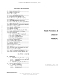
I/O Teach for Configuring Disk Controller
=E? C
create a copy of a LUN after another LUN
Controller LUN
=00? 0
Before or After [B,A] =A? (CR)
Controller LUN
=00? 4
Disk Controllers Available
LUN
Type
Address
# dev
0
VME147
$FFFE400 1
0
SCSI
Addr = 0
CDC
94161-9
1
VME147
$FFFE400 1
0
SCSI
Addr = 1
MICROP
1375
2
VME147
$FFFE400 1
0
SCSI
Addr = 2
CDC
94171-9
3
VME147
$FFFE400 1
0
SCSI
Addr = 3
SEAGAT
E
ST296N/
M
4
VME147
$FFFE400 1
0
SCSI
Addr = 4
ARCHIV
E
VIPER 60
5
VME147
$FFFE400 1
0
SCSI
Addr = 0
CDC
94161-9
6
VME147
$FFFE400 1
0
SCSI
Addr = 5
7
VME147
$FFFE400 4
0
SCSI
Addr = 6
SMS
OMTI700
0
9
VME320
$FFFFB00 4
0
A
VME350
$FFFF500 1
0
VME147
$FFFE400 *
0
21116
SCSI
Addr = 7
Quit options:
E
-Edit (edit another LUN)
Q
-Quit
3-57
3
3
THE 147Bug DEBUGGER COMMAND SET
S
-Save in NVRAM and quit
=Q? E
Edit another LUN
Disk Controllers Available
LUN
Type
Address
# dev
0
VME147
$FFFE400 1
0
SCSI
Addr = 0
CDC
94161-9
1
VME147
$FFFE400 1
0
SCSI
Addr = 1
MICROP
1375
2
VME147
$FFFE400 1
0
SCSI
Addr = 2
CDC
94171-9
3
VME147
$FFFE400 1
0
SCSI
Addr = 3
SEAGAT
E
ST296N/
M
4
VME147
$FFFE400 1
0
SCSI
Addr = 4
ARCHIV
E
VIPER 60
5
VME147
$FFFE400 1
0
SCSI
Addr = 0
CDC
94161-9
6
VME147
$FFFE400 1
0
SCSI
Addr = 5
7
VME147
$FFFE400 4
0
SCSI
Addr = 6
SMS
OMTI700
0
9
VME320
$FFFFB00 4
0
A
VME350
$FFFF500 1
0
VME147
$FFFE400 *
0
SCSI
Addr = 7
Disk Map edit commands:
C
3-58
-Copy
E
-Edit
M
-Move
21116
I/O Teach for Configuring Disk Controller
R
-Remove
=C? M
Move a LUN before another LUN
Controller LUN
=04? 6
Before or After [B,A] =A? B
Controller LUN
=06? 0
Disk Controllers Available
LUN
Type
Address
# dev
0
VME147
$FFFE400 1
0
SCSI
Addr = 5
1
VME147
$FFFE400 1
0
SCSI
Addr = 0
CDC
94161-9
2
VME147
$FFFE400 1
0
SCSI
Addr = 1
MICROP
1375
3
VME147
$FFFE400 1
0
SCSI
Addr = 2
CDC
94171-9
4
VME147
$FFFE400 1
0
SCSI
Addr = 3
SEAGAT
E
ST296N/
M
5
VME147
$FFFE400 1
0
SCSI
Addr = 4
ARCHIV
E
VIPER 60
6
VME147
$FFFE400 1
0
SCSI
Addr = 0
CDC
94161-9
7
VME147
$FFFE400 4
0
SCSI
Addr = 6
SMS
OMTI700
0
9
VME320
$FFFFB00 4
0
A
VME350
$FFFF500 1
0
VME147
$FFFE400 *
0
21116
SCSI
Addr = 7
Quit options:
3-59
3
3
THE 147Bug DEBUGGER COMMAND SET
E
-Edit (edit another LUN)
Q
-Quit
S
-Save in NVRAM and quit
=Q? E
Disk Controllers Available
LUN
Type
Address
# dev
0
VME147
$FFFE400 1
0
SCSI
Addr = 5
1
VME147
$FFFE400 1
0
SCSI
Addr = 0
CDC
94161-9
2
VME147
$FFFE400 1
0
SCSI
Addr = 1
MICROP
1375
3
VME147
$FFFE400 1
0
SCSI
Addr = 2
CDC
94171-9
4
VME147
$FFFE400 1
0
SCSI
Addr = 3
SEAGAT
E
ST296N/
M
5
VME147
$FFFE400 1
0
SCSI
Addr = 4
ARCHIV
E
VIPER 60
6
VME147
$FFFE400 1
0
SCSI
Addr = 0
CDC
94161-9
7
VME147
$FFFE400 4
0
SCSI
Addr = 6
SMS
OMTI700
0
8
VME320
$FFFFB00 4
0
9
VME350
$FFFF500 1
0
VME147
$FFFE400 *
0
Disk Map edit commands:
3-60
SCSI
Addr = 7
21116
I/O Teach for Configuring Disk Controller
C
-Copy
E
-Edit
M
-Move
R
-Remove
=M? R
Controller LUN
Remove a LUN
=00? 0
Disk Controllers Available
LUN
Type
Address
# dev
0
VME147
$FFFE400 1
0
SCSI
Addr = 0
CDC
94161-9
1
VME147
$FFFE400 1
0
SCSI
Addr = 1
MICROP
1375
2
VME147
$FFFE400 1
0
SCSI
Addr = 2
CDC
94171-9
3
VME147
$FFFE400 1
0
SCSI
Addr = 3
SEAGAT
E
ST296N/
M
4
VME147
$FFFE400 1
0
SCSI
Addr = 4
ARCHIV
E
VIPER 60
5
VME147
$FFFE400 1
0
SCSI
Addr = 0
CDC
94161-9
6
VME147
$FFFE400 4
0
SCSI
Addr = 6
SMS
OMTI700
0
8
VME320
$FFFFB00 4
0
9
VME350
$FFFF500 1
0
VME147
$FFFE400 *
0
21116
SCSI
Addr = 7
Quit options:
3-61
3
3
THE 147Bug DEBUGGER COMMAND SET
E
-Edit (edit another LUN)
Q
-Quit
S
-Save in NVRAM and quit
=Q? E
Disk Controllers Available
LUN
Type
Address
# dev
0
VME147
$FFFE400 1
0
SCSI
Addr = 0
CDC
94161-9
1
VME147
$FFFE400 1
0
SCSI
Addr = 1
MICROP
1375
2
VME147
$FFFE400 1
0
SCSI
Addr = 2
CDC
94171-9
3
VME147
$FFFE400 1
0
SCSI
Addr = 3
SEAGAT
E
ST296N/
M
4
VME147
$FFFE400 1
0
SCSI
Addr = 4
ARCHIV
E
VIPER 60
5
VME147
$FFFE400 1
0
SCSI
Addr = 0
CDC
94161-9
6
VME147
$FFFE400 4
0
SCSI
Addr = 6
SMS
OMTI700
0
8
VME320
$FFFFB00 4
0
9
VME350
$FFFF500 1
0
VME147
$FFFE400 *
0
SCSI
Addr = 7
Disk Map edit commands:
C
3-62
-Copy
21116
I/O Teach for Configuring Disk Controller
E
-Edit
M
-Move
R
-Remove
=R? E
Edit a LUN
Controller LUN
=00? 5
SCSI device [Y,N] =Y? Y
Controller type
= 0147? (\CR)
Controller address = $FFFE4000? (CR)
SCSI address (0-7) = 00? 5
SCSI Controller Type:
D
-
(147)
Teac Floppy
E
-
(147)
Omti (3500/7x00)
F
-
(147)
Common Command
Set (Win/Floppy)
F
-
(327)
Common Command
Set (Win)
10
-
(All)
CDC (Wren III &
Swift)
11
-
(All)
Micropolis 1375
12
-
(All)
Archive Viper, Teac
Tape
13
-
(All)
CDC (Wren IV & V),
Maxtor 8760
14
-
(All)
Seagate
15
-
(327)
Common Command
Set Rev. 4A (Win)
16
-
(All)
Kennedy, HP 1/2"
Tape
17
-
(147)
Sync Common
Command Set
(Win/Floppy)
17
-
(327)
Sync Common
Command Set (Win)
18
-
(All)
Exabyte Tape
19
-
(All)
IBM
3-63
3
3
THE 147Bug DEBUGGER COMMAND SET
1A
-
(327)
SONY
=10? (CR)
Number of supported devices = 1
DLUN 0 is a Fixed Disk Device
Disk Controllers Available
LUN
Type
Address
# dev
0
VME147
$FFFE400 1
0
SCSI
Addr = 0
CDC
94161-9
1
VME147
$FFFE400 1
0
SCSI
Addr = 1
MICROP
1375
2
VME147
$FFFE400 1
0
SCSI
Addr = 2
CDC
94171-9
3
VME147
$FFFE400 1
0
SCSI
Addr = 3
SEAGAT
E
ST296N/
M
4
VME147
$FFFE400 1
0
SCSI
Addr = 4
ARCHIV
E
VIPER 60
5
VME147
$FFFE400 1
0
SCSI
Addr = 5
6
VME147
$FFFE400 4
0
SCSI
Addr = 6
SMS
OMTI700
0
8
VME320
$FFFFB00 4
0
9
VME350
$FFFF500 1
0
VME147
$FFFE400 *
0
SCSI
Addr = 7
Quit options:
E
3-64
-Edit (edit another LUN)
21116
I/O Teach for Configuring Disk Controller
Q
-Quit
S
-Save in NVRAM and quit
=Q? S
Save in NVRAM and quit
147-Bug>
When invoked without options, the IOT command enters an interactive
subcommand mode where the descriptor table values currently in effect are
displayed one-at-a-time on the screen for you to examine. You may change the
displayed value by entering a new value or leave it unchanged.
The first two items of information that you are prompted for are the controller
LUN and the device LUN (LUN = Logical Unit Number). These two LUNs
specify one particular drive out of many that may be present in the system.
If the controller LUN and device LUN selected do not correspond to a valid
controller and device, IOT outputs the message "Invalid LUN" and you are
prompted for the two LUNs again.
147-Bug>IOT
Edit Disk Map [Y,N] N? (CR)
Controller LUN
= 00? (CR)
Device LUN
= 00? (CR)
Controller type
= VME147
Controller address = $FFFE4000? (CR)
VME147 Controller SCSI address (0-7) = 07? (CR)SCSI Only
SCSI Controller Type:SCSI Only
D
-
(147)
Teac Floppy
E
-
(147)
Omti (3500/7x00)
F
-
(147)
Common Command
Set (Win/Floppy)
F
-
(327)
Common Command
Set (Win)
10
-
(All)
CDC (Wren III &
Swift)
11
-
(All)
Micropolis 1375
3-65
3
3
THE 147Bug DEBUGGER COMMAND SET
12
-
(All)
Archive Viper, Teac
Tape
13
-
(All)
CDC (Wren IV & V),
Maxtor 8760
14
-
(All)
Seagate
15
-
(327)
Common Command
Set Rev. 4A (Win)
16
-
(All)
Kennedy, HP 1/2"
Tape
17
-
(147)
Sync Common
Command Set
(Win/Floppy)
17
-
(327)
Sync Common
Command Set (Win)
18
-
(All)
Exabyte Tape
19
-
(All)
IBM
1A
-
(327)
SONY
=10? (CR)
After the parameter table for one particular drive has been selected via a
controller LUN and a device LUN, IOT begins displaying the values in the
attribute fields, allowing you to enter changes if desired.
The parameters and attributes that are associated with a particular device are
determined by a parameter and an attribute mask that is a part of the device
definition. The device that has been selected may have any combination of the
following parameters and attributes:
1.
Sector Size:
0-128 1-256
2-512 3-1024
=01?
The physical sector size specifies the number of data bytes per
sector.
2.
3-66
Block Size:
0-128 1-256
2-512 3-1024
=01?
I/O Teach for Configuring Disk Controller
The block size defines the units in which a transfer count is
specified when doing a disk/tape block transfer. The block
size can be smaller, equal to, or greater than the physical
sector size, as long as the following relationship holds true:
(Block Size)*(Number of Blocks)/(Physical Sector Size) must
be an integer.
3.
Sectors/Track
=0020?
This field specifies the number of data sectors per track, and
is a function of the device being accessed and the sector size
specified.
4.
Starting Head
=10?
This field specifies the starting head number for the device. It
is normally zero for Winchester and floppy drives. It is
nonzero for dual volume SMD drives.
5.
Number of Heads
=05?
This field specifies the number of heads on the drive.
6.
Number of Cylinders =0337?
This field specifies the number of cylinders on the device. For
floppy disks, the number of cylinders depends on the media
size and the track density. General values for 5-1/4 inch
floppy disks are shown below:
48 TPI - 40 cylinders
96 TPI - 80 cylinders
7.
Precomp. Cylinder
=0000?
This field specifies the cylinder number at which
precompensation should occur for this drive. This parameter
is normally specified by the drive manufacturer.
8.
Reduced Write Current Cylinder =0000?
This field specifies the cylinder number at which the write
current should be reduced when writing to the drive. This
parameter is normally specified by the drive manufacturer.
9.
Interleave Factor
=00?
This field specifies how the sectors are formatted on a track.
Normally, consecutive sectors in a track are numbered
sequentially in increments of 1 (interleave factor of 1). The
3-67
3
3
THE 147Bug DEBUGGER COMMAND SET
interleave factor controls the physical separation of logically
sequential sectors. This physical separation gives the host
time to prepare to read the next logical sector without
requiring the loss of an entire disk revolution.
10. Spiral Offset
=00?
The spiral offset controls the number of sectors that the first
sector of each track is offset from the index pulse. This is used
to reduce latency when crossing track boundaries.
11. ECC Data Burst Length =0000?
This field defines the number of bits to correct for an ECC
error when supported by the disk controller.
12. Step Rate Code
=00?
The step rate is an encoded field used to specify the rate at
which the read/write heads can be moved when seeking a
track on the disk.
The encoding is as follows:
00
STEP RATE
WINCHESTER
SLOW
FAST
CODE (HEX)
HARD DISKS
DATA RATE
DATA RATE
0 ms
12 ms
6 ms
01
6 ms
6 ms
3 ms
02
10 ms
12 ms
6 ms
03
15 ms
20 ms
10 ms
04
20 ms
30 ms
15 ms
13. Single/Double DATA Density =D (S/D)?
Single (FM) or double (MFM) data density should be specified
by typing S or D, respectively.
14. Single/Double TRACK Density =D (S/D)?
Used to define the density across a recording surface. This
usually relates to the number of tracks per inch as follows:
48 TPI = Single Track Density
96 TPI = Double Track Density
15. Single/Equal_in_all Track zero density =S (S/E)?
3-68
I/O Teach for Configuring Disk Controller
This flag specifies whether the data density of track 0 is a
single density or equal to the density of the remaining tracks.
For the "Equal_in_all" case, the Single/Double data density
flag indicates the density of track 0.
16. Slow/Fast Data Rate =S (S/F)?
This flag selects the data rate for floppy disk devices as
follows:
S = 250 kHz data rate (5-1/4 inch floppy, usually)
F = 500 kHz data rate (8-inch, 3-1/2 inch floppy, usually)
17. Gap 1
=07?
This field contains the number of words of zeros that are
written before the header field in each sector during format.
18. Gap 2
=08?
This field contains the number of words of zeros that are
written between the header and data fields during format and
write commands.
19. Gap 3
=00?
This field contains the number of words of zeros that are
written after the data fields during format commands.
20. Gap 4
=00?
This field contains the number of words of zeros that are
written after the last sector of a track and before the index
pulse.
21. Spare Sectors Count =00?
This field contains the number of sectors per track allocated as
spare sectors. These sectors are only used as replacements for
bad sectors on the disk.
Example 1:
Examining the default parameters of a 5-1/4 inch floppy disk.
147-Bug>IOT
Edit Disk Map [Y,N] N? (CR)
Controller LUN
=00? 8
Device LUN
=00? 2
Controller type
=VME320
3-69
3
3
THE 147Bug DEBUGGER COMMAND SET
Controller address
=$FFFFB000? (CR)
Sector Size:
0-128 1-256
2-512 3-1024
=01? (CR)
Block Size:
0-128 1-256
2-512 3-1024
=01? (CR)
Sectors/track
=0010? (CR)
Number of heads
=02? (CR)
Number of cylinders =0050? (CR)
Precomp. Cylinder
=0028? (CR)
Step Rate Code
=00? (CR)
Single/Double TRACK density=D (S/D)? (CR)
Single/Double DATA density =D (S/D)? (CR)
Single/Equal_in_all Track zero density =S (S/E)? (CR)
Slow/Fast Data Rate =S (S/F)? (CR)
147-Bug>
Example 2:
Changing from a 40Mb Winchester to a 70Mb Winchester. (Note that
reconfiguration such as this is only necessary when the device is not formatted
or of an unknown format, or has no configuration sector. Reconfiguration is
normally done automatically by the IOP, BO, or BH commands.
147-Bug>IOT
Edit Disk Map [Y,N] N? (CR)
Controller LUN
=00? 8
Device LUN
=00? (CR)
Controller type
=VME320
Controller address
=$FFFFB000? (CR)
Sector Size:
0-128 1-256
2-512 3-1024
=01? (CR)
Block Size:
0-128 1-256
2-512 3-1024
=01? (CR)
Sectors/track
=0020? (CR)
Starting head
=00? (CR)
Number of heads
=06? 8
Number of cylinders =033E? 400
Precomp. Cylinder
=0000? 401
Reduced Write Current Cylinder=0000? (CR)
3-70
Load S-Records From Host
Interleave factor
=01? 0B
Spiral Offset
=00? (CR)
ECC Data Burst Length=0000? 000B
Reserved Area Units:Tracks/Cylinders =T (T/C)? (CR)
Tracks Reserved for Alternates=0000? (CR)
147-Bug>
Load S-Records From Host
LO [n] [addr] [;x|-c|t] [=text]
This command is used when data in the form of a file of Motorola S-records is
to be downloaded from a host system to the MVME147. The LO command
accepts serial data from the host and loads it into memory.
N ote
The highest baud rate that can be used with the LO
command (downloader) is 9600 baud.
The optional port number "n" allows you to specify which port is to be used for
the downloading. If this number is omitted, port 1 is assumed.
The optional addr field allows you to enter an offset address which is to be
added to the address contained in the address field of each record. This causes
the records to be stored to memory at different locations than would normally
occur. The contents of the automatic offset register are not added to the Srecord addresses. If the address is in the range $0 to $1F and the port number
is omitted, enter a comma before the address to distinguish it from a port
number.
The optional text field, entered after the equals sign (\o’==’), is sent to the host
before 147Bug begins to look for S-records at the host port. This allows you to
send a command to the host device to initiate the download. This text should
NOT be delimited by any kind of quote marks. Text is understood to begin
immediately following the equals sign and terminate with the carriage return.
If the host is operating full duplex, the string is also echoed back to the host
port by the host and appears on your terminal screen.
In order to accommodate host systems that echo all received characters, the
above-mentioned text string is sent to the host one character at a time and
characters received from the host are read one at a time. After the entire
command has been sent to the host, LO keeps looking for a LF character from
3-71
3
3
THE 147Bug DEBUGGER COMMAND SET
the host, signifying the end of the echoed command. No data records are
processed until this LF is received. If the host system does not echo characters,
LO still keeps looking for a LF character before data records are processed.
For this reason, it is required in situations where the host system does not echo
characters, that the first record transferred by the host system be a header
record. The header record is not used but the LF after the header record serves
to break LO out of the loop so that data records are processed.
The other options have the following effects:
-c
-
Ignore checksum. A checksum for the data contained within an S-record is
calculated as the S-record is read in at the port. Normally, this calculated
checksum is compared to the checksum contained within the S-record and
if the compare fails, an error message is sent to the screen on completion of
the download. If this option is selected, the comparison is not made.
-
Echo. This option echoes the S-records to your terminal as they are read in
at the host port.
-
TRAP #15 code. This option causes LO to set the target register D4 =’LO ’x,
with x =$0C ($4C4F200C). The ASCII string ’LO ’ indicates that this is the
LO command; the code $0C indicates TRAP #15 support with stack
parameter/result passing and TRAP #15 disk support. This code can be
used by the downloaded program to select the appropriate calling
convention when invoking debugger functions, because some Motorola
debuggers use conventions different from 147Bug, and they set a different
code in D4.
option
x
option
t
option
The S-record format (refer to Appendix C) allows for an entry point to be
specified in the address field of the termination record of an S-record block.
The contents of the address field of the termination record (plus the offset
address, if any) are put into the target PC. Thus, after a download, you need
only enter G or GO instead of G addr or GO addr to execute the code that was
downloaded.
If a nonhex character is encountered within the data field of a data record, the
part of the record which had been received up to that time is printed to the
screen and the 147Bug error handler is invoked to point to the faulty character.
As mentioned, if the embedded checksum of a record does not agree with the
checksum calculated by 147Bug AND if the checksum comparison has not
been disabled via the "-c" option, an error condition exists. A message is
output stating the address of the record (as obtained from the address field of
3-72
Load S-Records From Host
the record), the calculated checksum, and the checksum read with the record.
A copy of the record is also output. This is a fatal error and causes the
command to abort.
When a load is in progress, each data byte is written to memory and then the
contents of this memory location are compared to the data to determine if the
data stored properly. If for some reason the compare fails, a message is output
stating the address where the data was to be stored, the data written, and the
data read back during the compare. This is also a fatal error and causes the
command to abort.
Because processing of the S-records is done character-by-character, any data
that was deemed good has already been stored to memory if the command
aborts due to an error.
Examples: Suppose a host system (using VERSAdos in this case) was used to
create this program:
1
2
3
65040000
4
5
6504000 7001
6
6504002 D088
7
6504004 4A00
8
6504006 4E75
9
****** TOTAL ERRORS
****** TOTAL WARNINGS
*
*
Test Program.
ORG
$65040000
MOVEQ.L
ADD.L
TST.B
RTS
END
#$1,D0
A0,D0
D0
0-0--
Then this program was compiled and converted into an S-record file named
TEST.MX as follows:
S00F00005445535453335337202001015E
S30D650400007001D0884A004E75B3
S7056504000091
Load this file into MVME147 memory for execution at address $40000 as
follows:
147-Bug>TMGo into transparent mode to establish
Escape character: $01= ^
communication with the host.
‘’
<BREAK>Press BREAK key to get login prompt.
3-73
3
3
THE 147Bug DEBUGGER COMMAND SET
‘’
(login)You must log onto the host and enter the
‘’ proper directory to access the file TEST.MX
‘’
= <^
to 147Bug prompt.
147-Bug>LO -65000000 ;x=copy TEST.MX,#
COPY TEST.MX,#
S00F00005445535453335337202001015E
S30D650400007001D0884A004E75B3
S7056504000091
147-Bug>
The S-records are echoed to the terminal because of the x option.
The offset address of -65000000 was added to the addresses of the records in
FILE.MX and caused the program to be loaded to memory starting at $40000.
The text copy TEST.MX,# is a VERSAdos command line that caused the file to
be copied by VERSAdos to the port which is connected with the MVME147
host port.
147-Bug>MD 40000:4;DI <CR>
00040000 7001
00040002 D088
00040004 4A00
00040006 4E75
147-Bug>
MOVEQ.L
ADD.L
TST.B
RTS
#$1,D0
A0,D0
D0
The target PC now contains the entry point of the code in memory ($40000).
LAN Station Address Display/Set
LSAD
The LSAD command is used for examining and updating the Ethernet station
address.
Every MVME147 with LAN support is assigned an Ethernet station address.
The address is $08003E2xxxxx where xxxxx is the unique number assigned to
the module; i.e., every MVME147 has a different value for xxxxx).
3-74
Macro Define/Display/Delete
Each Ethernet station address is displayed on a label attached to the back of the
MVME147 front panel. In addition, the xxxxx portion of the Ethernet station
address is stored in BBRAM, location $FFFE0778 as $2xxxxx.
If Motorola networking software is running on an MVME147, it uses the
2xxxxx value from BBRAM to complete the Ethernet station address
($08003E2xxxxx). The user must assure that the value of 2xxxxx is maintained
in BBRAM. If the value of 2xxxxx is lost in BBRAM, the user should use
number on the front panel label to restore it. Note that MVME147bug includes
the LSAD command for examining and updating the BBRAM xxxxx value.
Example 1:
display Ethernet station address
147-Bug> LSAD
LAN Station Address = $08003E200000
To set the Station Address:
Enter the code located on the back of the front panel:
$08003E2_____(CR)
147-Bug>
Example 2:
change Ethernet station address
147-Bug> LSAD
LAN Station Address = $08003E200000
To set the Station Address:
Enter the code located on the back of the front panel:
$08003E2_____1
LAN Station Address = $08003E200001
147-Bug>
Macro Define/Display/Delete
MA [name]
NOMA [name]
The name can be any combination of 1 through 8 alphanumeric characters.
The MA command allows you to define a complex command consisting of any
number of debugger primitive commands with optional parameter
specifications.
3-75
3
3
THE 147Bug DEBUGGER COMMAND SET
NOMA command is used to delete either a single macro or all macros.
Entering MA without specifying a macro name causes the debugger to list all
currently defined macros and their definitions.
When MA is invoked with the name of a currently defined macro, that macro
definition is displayed.
Line numbers are shown when displaying macro definitions to facilitate
editing via the MAE command. If MA is invoked with a valid name that does
not currently have a definition, then the debugger enters the macro definition
mode. In response to each macro definition prompt "M\o’==’", enter a
debugger command, including a carriage return. Commands entered are not
checked for syntax until the macro is invoked. To exit the macro definition
mode, enter only a carriage return (null line) in response to the prompt. If the
macro contains errors, it can either be deleted and redefined or it can be edited
with the MAE command. A macro containing no primitive debugger
commands; i.e., no definition, is not accepted.
Macro definitions are stored in a string pool of fixed size. If the string pool
becomes full while in the definition mode, the offending string is discarded, a
message STRING POOL FULL, LAST LINE DISCARDED is printed and you
are returned to the debugger command prompt. This also happens if the
string entered would cause the string pool to overflow. The string pool has a
capacity of 511 characters. The only way to add or expand macros when the
string pool is full is either to delete or edit macro(s).
Debugger commands contained in macros may reference arguments supplied
at invocation time. Arguments are denoted in macro definitions by
embedding a back slash "\\" followed by a numeral. Up to ten arguments are
permitted. A definition containing a back slash followed by a zero would
cause the first argument to that macro to be inserted in place of the "\0"
characters. Similarly, the second argument would be used whenever the
sequence "\\\1" occurred.
Thus, entering ARGUE 3000 1 ;B on the debugger command line would
invoke the macro named ARGUE with the text strings 3000, 1, and ;B replacing
"\0" , "\\\1", and "\\\2" respectively, within the body of the macro.
To delete a macro, invoke NOMA followed by the name of the macro.
Invoking NOMA without specifying a macro name deletes all macros. If
NOMA is invoked with a macro name that does not have a definition, an error
message is printed.
Examples:
3-76
Macro Define/Display/Delete
147-Bug> MA ABC
M=MD 3000
M=GO \0
M= (CR)
147-Bug>
define macro ABC
147-Bug> MA DIS
M=MD \0:17;DI
M= (CR)
147-Bug>
define macro DIS
147-Bug> MA
MACRO ABC
010 MD 3000
020 GO \0
MACRO DIS
010 MD \0:17;DI
147-Bug>
list macro definitions
147-Bug> MA ABC
MACRO ABC
010 MD 3000
020 GO \0
147-Bug>
list definition of macro ABC
147-Bug> NOMA DIS
147-Bug>
delete macro DIS
147-Bug> MA ASM
M=MM \0;DI
M= (CR)
147-Bug>
define macro ASM
147-Bug> MA
MACRO ABC
010 MD 3000
020 GO \0
MACRO ASM
010 MM \0;DI
147-Bug>
list all macros
147-Bug> NOMA
147-Bug>
delete all macros
147-Bug> MA
NO MACROS DEFINED
147-Bug>
list all macros
3-77
3
3
THE 147Bug DEBUGGER COMMAND SET
Macro Edit
MAE name line# [string]
name
Any combination of 1 through 8
alphanumeric characters.
line#
Line number in range 1 through 999.
string
Replacement line to be inserted.
The MAE command permits modification of the macro named in the
command line. MAE is line oriented and supports the following actions:
insertion, deletion, and replacement.
To insert a line, specify a line number between the numbers of the lines that
the new line is to be inserted between. The text of the new line to be inserted
must also be specified on the command line following the line number.
To replace a line, specify its line number and enter the replacement text after
the line number on the command line.
A line is deleted if its line number is specified and the replacement line is
omitted.
Attempting to delete a nonexistent line results in an error message being
displayed. MAE does not permit deletion of a line if the macro consists only
of that line. NOMA must be used to remove a macro. To define new macros,
use MA; the MAE command operates only on previously defined macros.
Line numbers serve one purpose: specifying the location within a macro
definition to perform the editing function. After the editing is complete, the
macro definition is displayed with a new set of line numbers.
Examples:
147-Bug> MA ABC
MACRO ABC
010 MD 3000
020 GO \0
147-Bug>
3-78
list definition of macro ABC
Enable/Disable Macro Expansion Listing
147-Bug> MAE ABC 15 RD
add a line to macro ABC
MACRO ABC
010 MD 3000
020 RD
this line was inserted
030 GO \0
147-Bug>
147-Bug> MAE ABC 10 MD
replace line 10
10+R0
MACRO ABC
010 MD 10+R
this line was overwritten
020 RD
030 GO \0
147-Bug>
147-Bug> MAE ABC 30
delete line 30
MACRO ABC
010 MD 10+R0
020 RD
147-Bug>
Enable/Disable Macro Expansion Listing
MAL
NOMAL
The MAL command allows you to view expanded macro lines as they are
executed. This is especially useful when errors result, as the
line that caused the error appears on the display.
The NOMAL command is used to suppress the listing of the macro lines
during execution.
The use of MAL and NOMAL is a convenience for you and in no way
interacts with the function of the macros.
Save/Load Macros
MAW [controller LUN][del[device LUN][del block #]]
MAR [controller LUN][del[device LUN][del block #]]
3-79
3
3
THE 147Bug DEBUGGER COMMAND SET
controller
LUN
is the logical unit number of the controller to which
the following device is attached. Initially defaults to
LUN 0.
device LUN
is the logical unit number of the device to save/load
macros to/from. Initially defaults to LUN 0.
del
is a field delimiter:
block #
is the number of the block on the above device that is
the first block of the macro list. Initially defaults
to block 2.
comma (,), or spaces ( ).
The MAW command allows you to save the currently defined macros to
disk/tape. A message is printed listing the block number,
controller LUN, and device LUN before any writes are made. This
message is followed by a prompt (OK to proceed (y/n)?). You may
then decline to save the macros by typing the letter N (uppercase
or lowercase). Typing the letter Y (uppercase or lowercase) permits MAW
to proceed to write the macros out to disk/tape. The list is saved as a
series of strings and may take up to three blocks. If no macros
are currently defined, no writes are done to disk/tape and NO
MACRO DEFINED is displayed.
The MAR command allows you to load macros that have previously been
saved by MAW. Care should be taken to avoid attempting to load macros
from a location on the disk/tape other than that written to by the
MAW command. While MAR check for invalid macro names and other
anomalies, the results of such a mistake are unpredictable.
N ote
MAR discards all currently defined macros before loading
from disk/tape.
Defaults change each time MAR and MAW are invoked. When either has
been used, the default controller, device, and block numbers are
set to those used for that command. If macros were loaded from
controller 0, device 2, block 8 via command MAR, the the defaults
for a later invocation of MAW or MAR would be controller 0, device 2,
and block 8.
Errors encountered during I/O are reported along with the 16-bit
status word returned by the I/O routines.
3-80
Memory Modify
Examples:
Assume that controller 0, device 2 is accessible
147-Bug> MAR 0,2,3
load macros from block 3
147-Bug>
147-Bug> MA
list macros
MACRO ABC
010 MD 3000
020 GO \0
147-Bug>
147-Bug> MA ASM
define macro ASM
M=MM \0;DI
M= (CR)
147-Bug>
147-Bug> MA
list all macros
MACRO ABC
010 MD 3000
020 GO \0
MACRO ASM
010 MM \0;DI
147-Bug>
147-Bug> MAW ,,8
save macros to block 8, previous device
WRITING TO BLOCK $8 ON CONTROLLER $0, DEVICE $2
OK to proceed (y/N)? Y carriage return not needed
147-Bug>
Memory Modify
MM addr[;[[b|w|l|s|d|x|p][a][n] ]|[di]]
The M or MM command is used to examine and change memory locations.
MM accepts the following data types:
Integer Data Type
Floating-Point Data Type
b
Byte
s
Single Precision
w
Word
d
Double Precision
3-81
3
3
THE 147Bug DEBUGGER COMMAND SET
Integer Data Type
Longword
l
Floating-Point Data Type
x
Extended Precision
p
Packed Precision
The default data type is word. The MM command (alternate form M) reads
and displays the contents of memory at the specified address and prompts you
with a question mark ("?"). You may enter new data for the memory location,
followed by CR, or you may simply enter CR, which leaves the contents
unaltered. That memory location is closed and the next location is opened.
Refer to Chapter 2 for use of a function code as part of the addr field.
You may also enter one of several special characters, either at the prompt or
after writing new data, which change what happens when the carriage return
is entered. These special characters are as follows:
V or v
The next successive memory location is opened. (This is the default. It is in
effect whenever MM is invoked and remains in effect until changed by
entering one of the other special characters.)
^
MM backs up and opens the previous memory location.
\o’==’
MM re-opens the same memory location (this is useful for examining I/O
registers or memory locations that are changing over time).
.
Terminates MM command. Control returns to 147Bug.
The n option of the MM command disables the read portion of the command.
The a option forces alternate location accesses only.
Example 1:
147-Bug>MM 10000
access location 10000.
00010000 1234? (CR)
00010002 5678? 4321
modify memory.
00010004 9ABC? 8765^
modify memory and backup.
00010002 4321? (CR)
00010000 1234? abcd.
Example 2:
3-82
modify memory and exit.
Memory Modify
147-Bug>MM 10001;la
longword access to location 10001.
00010001 CD432187? (CR)
alternate location accesses.
00010009 00068010? 68010+10=
modify and reopen location.
00010009 00068020? (CR)
00010009 00068020? .
exit MM.
The di option enables the one-line assembler/disassembler. All other options
are invalid if di is selected. The contents of the specified memory location are
disassembled and displayed and you are prompted with a question mark ("?")
for input. At this point, you have three options:
1.
Enter (CR). This closes the present location and continues with
disassembly of next instruction.
2.
Enter a new source instruction followed by <CR>. This invokes the
assembler, which assembles the instruction and generates a "listing file" of
one instruction.
3.
Enter . (CR). This closes the present location and exits the MM command.
If a new source line is entered (choice 2 above), the present line is erased and
replaced by the new source line entered. In the hardcopy mode, a linefeed is
done instead of erasing the line.
If an error is found during assembly, the symbol ^ appears below the field
suspected of the error, followed by an error message. The location being
accessed is redisplayed.
For additional information about the assembler, refer to Chapter 4.
The examples below were made in the hardcopy mode.
Example 3:
Assemble a new source line.
147-Bug>MM 10000;di
00010000 46FC2400
00010000 85E2
00010002 2400
147-Bug>
Example 4:
MOVE.W
DIVS.W
MOVE.L
$2400,SR ? divs.w -(A2),D2
-(A2),D2
D0,D2 ? (CR)
New source line with error.
3-83
3
3
THE 147Bug DEBUGGER COMMAND SET
00010008 4E7AD801
MOVEC.L VBR,A5 ? bchg #$12,9(A5,D6))
00010008
BCHG
#$12,9(A5,D6))
--------------------------------------------------^
*** Unknown Field ***
00010008 4E7AD801
MOVEC.L VBR, A5 ? (CR)
147-Bug>
Example 5:
Step to next location and exit MM.
147-Bug>M 1000C;di
FFE1000C 000000FF
FFE10010 20C9
147-Bug>
OR.B
MOVE.L
#255,D0 ? (CR)
A1,(A0)+ ? .
Example 6:
147-Bug>M 7000;X
00007000 0_0000_FFFFFFFF00000000?1_3C10_84782
0000700C 1_7FFF_00000000FFFFFFFF?0_001A_F
00007018 0_0000_FFFFFFFF00000000?6.02E23=
00007018 0_404D_FEF4F885469B0880?^
0000700C 0_001A_F000000000000000?(CR)
00007000 1_3C10_8478200000000000?.
147-Bug>
Memory Display
MD[s]addr[:count | addr][; [b|w|l|s|d|x|p]di] ]
This command is used to display the contents of multiple memory locations all
at once. MD accepts the following data types:
Integer Data Type
Floating-Point Data Type
b
Byte
s
Single Precision
w
Word
d
Double Precision
l
Longword
x
Extended Precision
p
Packed Precision
3-84
Memory Display
The default data type is word. Also, for the integer data types, the data is
always displayed in hex along with its ASCII representation. The di option
enables the Resident MC68030 disassembler. No other option is allowed if di
is selected.
Refer to Chapter 2 for use of a function code as part of the addr field.
The optional count argument in the MD command specifies the number of
data items to be displayed (or the number of disassembled instructions to
display if the disassembly option is selected) defaulting to 8 if none is entered.
The default count is changed to 128 if the s (sector) modifier is used. Entering
only CR at the prompt immediately after the command has completed causes
the command to re-execute, displaying an equal number of data items or lines
beginning at the next address.
Example 1:
147-Bug>MD 12000
00012000 2800 1942 2900 1942
(..B)..B(..B).(F
147-Bug>(CR)
00012010 FC20 0050 ED07 9F61
.Pm..a....h’p’
2800 1842 2900 2846
FF00 000A E860 F060
|
Example 2: Assume the following processor state: A2=00013500,
D5=53F00127.
147-Bug>MD (A2,D5):&19;b
00013627 4F 82 00 C5 9B 10 33 7A
O..E..3z_.l=KP..
00013637 31 AB 80
147-Bug>
Example 3:
DF 01 6C 3D 4B 50 0F 0F
+1.
Disassemble eight instructions, starting at $50008
3-85
3
3
THE 147Bug DEBUGGER COMMAND SET
147-Bug>MD 50008;di
00050008 46FC2700
0005000C 61FF0000023E
00050012 4E7AD801
00050016 41ED7FFC
0005001A 5888
0005001C 2E48
0005001E 2C48
00050020 13C7FFFB003A
147-Bug>
MOVE.W
BSR.L
MOVEC.L
LEA.L
ADDQ.L
MOVE.L
MOVE.L
MOVE.B
$9984,SR
$5024C
VBR,A5
32764(A5),A0
$4,A0
A0,A7
A0,A6
D7,($FFFB003A).L
Example 4: To display eight double precision floating point numbers at location
50008, the user enters the following command line.
147-Bug>MD 50008;d
00005000 0_3F6_44C1D0F047FC2=
00005008 0_423_DAEFF04800000=
00005010 0_000_0000000000000=
00005018 0_403_0000000000000=
00005020 0_3FF_0000000000000=
00005028 0_000_00000FFFFFFFF=
00005030 0_44D_FDE9F10A8D361=
00005038 0_3C0_79CA10C924223=
147-Bug>
2.4777000000000002_E-0003
1.2749000000000000_E+0011
0.0000000000000000_E+0000
1.6000000000000000_E+0001
1.0000000000000000_E+0000
2.1219957904712067_E+0314
6.0200000000000000_E+0023
1.5999999999999999_E+0019
Menu
MENU
The MENU command works only if the 147Bug is in the "system" mode (refer
to the ENV command). When invoked in the "system" mode, it provides a way
to exit 147Bug and return to the menu.
The following is an example of command line entries and their definitions.
147-Bug>MENU
1
2
3
4
5
3-86
Continue System Start Up
Select Alternate Boot Device
Go to System Debugger
Initiate Service Call
Display System Test Errors
Memory Set
6 Dump Memory to Tape
Enter Menu #:
When the 147Bug is in "system" mode, you can toggle back and forth between
the menu and Bug by typing a 3 in response to the Enter Menu #: prompt when
the menu is displayed. Entering the Bug and then typing MENU in response
to the 147-Bug (or 147-Diag) prompt to return to the system menu.
For details on use of the system mode menu features, refer to Appendix A.
Memory Set
MS addr [hexadecimal number]. . . | [’string’]. . .
Memory set is used to write data to memory starting at the specified address.
Hex numbers are not assumed to be of a particular size, so they can contain
any number of digits (as allowed by command line buffer size). If an odd
number of digits are entered, the least significant nibble of the last byte
accessed is unchanged.
Refer to Chapter 2 for use of a function code as part of the addr field.
ASCII strings can be entered by enclosing them in single quotes (’). To include
a quote as part of a string, two consecutive quotes should be entered.
Example: Assume that memory is initially cleared:
147-Bug>MS 25000 0123456789abcDEF ’This is ’’147Bug’’’ 23456
147-Bug>MD 25000:10
00025000 0123 4567 89AB CDEF 5468 6973 2069 7320
.#Eg.+MoThis
is.
00025010 2731 3437 4275 6727 2345 6000 0000 0000
’147Bug’#E‘.....
147-Bug>
Set Memory Address from VMEbus
OBA
The OBA (Off-Board Address) command allows you to set the base address of
the MVME147 onboard RAM, as seen from the VMEbus (refer to Chapter 1).
Therefore, you should enter the hex number corresponding to the actual base
address, so that the offboard external devices on the VMEbus will know where
3-87
3
3
THE 147Bug DEBUGGER COMMAND SET
it is. The default condition is with the offboard address set to $0. These
selections are stored in the BBRAM that is part of the MK48T02 (RTC), and
remain in effect through power up or any reset.
Example 1: Display base addresses for 8Mb board
147-Bug>OBA
RAM address from VMEbus = $00000000? 1234Note 1
Base addresses are: $00000000, $00800000, $01000000, $01800000,
$02000000, $02800000, $03000000, $03800000,
$04000000, $04800000, $05000000, $05800000,
$06000000, $06800000, $07000000, $07800000,
$08000000, $08800000, $09000000, $09800000,
$0A000000, $0A800000, $0B000000, $0B800000,
$0C000000, $0C800000, $0D000000, $0D800000
RAM address from VMEbus = $00000000? (CR)Note 2
147-Bug>
Example 2:
Change base address for 8Mb board
147-Bug>OBA
RAM address from VMEbus = $00000000? 800000Note 3
147-Bug>
Example 3:
Display/change base address for 16Mb board
147-Bug>OBA
RAM address from VMEbus = $00000000? 1234
Base addresses are: $00000000, $01000000, $02000000, $03000000,
$04000000, $05000000, $06000000, $07000000,
$08000000, $09000000, $0A000000, $0B000000,
$0C000000, $0D000000, $0E000000, $0F000000,
$10000000, $11000000, $12000000, $13000000,
$10000000, $15000000, $16000000, $17000000,
$10000000, $19000000, $1A000000, $1B000000
Base Address options: 1, 2
3-88
Offset Registers Display/Modify
16/32 Mbyte Extended/Standard Addressing options available:
1 = Extended - $00000000-$00FFFFFF, Standard - $000000-$7FFFFF
2 = Extended - $01000000-$01FFFFFF, Standard - $000000-$7FFFFF
RAM address from VMEbus = $00000000? 2Note 4
147-Bug>
Example 4:
Change base address without option
147-Bug>OBA
RAM address from VMEbus (option 2) = $01000000? 0Note 5
147-Bug>
NOTES
:
1.
Any value that is not a base address or option, displays the base
addresses for the board based on the onboard RAM size.
2.
Pressing return without entering an address preserves the current
address.
3.
Change base address from $0 to $800000.
4.
Select option 2, onboard RAM responds to extended addresses from
$01000000 to $01FFFFFF, and standard addresses from $000000 to
$7FFFFF.
5.
Return the base address to the default address of $0. Onboard RAM
responds to extended addresses from $0 to end of onboard RAM, and
standard addresses from $0 to $FFFFFF.
Offset Registers Display/Modify
OF [ Rn[;A] ]
OF allows you to access and change pseudo-registers called offset registers.
These registers are used to simplify the debugging of relocatable and positionindependent modules. Refer to Chapter 2.
There are eight offset registers R0-R7, but only R0-R6 can be changed. R7
always has both base and top addresses set to 0. This allows the automatic
register function to be effectively disabled by setting R7 as the automatic
register.
3-89
3
3
THE 147Bug DEBUGGER COMMAND SET
Each offset register has two values: base and top. The base is the absolute least
address that is used for the range declared by the offset register. The top
address is the absolute greatest address that is used. When entering the base
and top, you may use either an address/address format or an address/count
format. If a count is specified, it refers to bytes. If the top address is omitted
from the range, then a count of 1Mb is assumed. The top address must equal
or exceed the base address. Wrap-around is not permitted.
Command usage:
OF
To display all offset registers. An asterisk indicates which register is
the automatic register.
OF Rn
To display/modify Rn. You can scroll through the register in a way
similar to that used by the MM command.
OF Rn;A
To display/modify Rn and set it as the automatic register. The
automatic register is one that is automatically added to each absolute
address argument of every command except if an offset register is
explicitly added. An asterisk indicates which register is the automatic
register.
Range entry
Ranges may be entered in three formats: base address alone, base and
top as a pair of addresses, and base address followed by byte count.
Control characters "^ used. Their function is identical to that in the
RM and MM commands.
Range syntax
[base address [del top address] ] [^
or
[base address [’.’ byte count ] ] [^
Offset register rules:
3-90
1.
At power up and cold start reset, R7 is the automatic register.
2.
At power up and cold start reset, all offset registers have both base and top
addresses preset to 0. This effectively disables them.
3.
R7 always has both base and top addresses set to 0; it cannot be changed.
4.
Any offset register can be set as the automatic register.
5.
The automatic register is always added to every absolute address
argument of every 147Bug command where there is not an offset register
explicitly called out.
Offset Registers Display/Modify
6.
There is always an automatic register. A convenient way to disable the
effect of the automatic register is by setting R7 as the automatic register.
Note that this is the default condition.
Examples:
Display offset registers.
147-Bug>OF
R0 =00000000
R2 =00000000
R4 =00000000
R6 =00000000
147-Bug>
00000000
00000000
00000000
00000000
R1 =
R3 =
R5 =
R7*=
00000000
00000000
00000000
00000000
00000000
00000000
00000000
00000000
Modify some offset registers.
147-Bug>OF R0
R0 =00000000 00000000? 20000 200FF
R1 =00000000 00000000? 25000:200^
R0 =00020000 000200FF? .
147-Bug>
Look at location $20000.
147-Bug>M 20000;DI
00000+R0
41F95445
147-Bug>M R0;DI
00000+R0
41F95445
147-Bug>
5354
LEA.L
($54455354).L,A0 .
5354
LEA.L
($54455354).L,A0 .
LEA.L
($54455354).L,A0 .
Set R0 as the automatic register.
147-Bug>OF R0;A
R0*=00020000 000200FF? .
To look at location $20000.
147-Bug>M 0;DI
00000+R0
41F95445
147-Bug>
5354
To look at location 0, override the automatic offset.
3-91
3
3
THE 147Bug DEBUGGER COMMAND SET
147-Bug>M 0+R7;DI
00000000
FFF8
147-Bug>
DC.W
$FFF8 .
Printer Attach/Detach
PA [n]
NOPA [n]
These two commands "attach" or "detach" a printer to the specified port.
Multiple printers may be attached. When the printer is attached, everything
that appears on the system console terminal is also echoed to the "attached"
port. PA is used to attach, NOPA is used to detach. If no port is specified, PA
does not attach any port, but NOPA detaches all attached ports.
If the port number specified is not currently assigned, PA displays an
"unassigned" message. If NOPA is attempted on a port that is not currently
attached, an "unassigned" message is displayed.
The port being attached must already be configured. This is done using the
Port Format (PF) command. This is done by executing the following sequence
prior to "PA n".
147-Bug>PF4
Logical unit $04 unassigned
Name of board? VME147
Name of port? PTR
Port base address = $FFFE2800? (CR)
DTE, DCE, or Printer [T,C,P] = P? (CR)
Auto Line Feed protocol [Y,N] = N? Y.
OK to proceed (y/n)? Y
147-Bug>
For further details, refer to the PF command.
Examples:
CONSOLE DISPLAY:PRINTER OUTPUT:
3-92
Port Format/Detach
147-Bug>PA4attach printer port 4
147-Bug>HE NOPA147-Bug>HE NOPA
NOPA
Printer DetachNOPA
Printer Detach
147-Bug>NOPA147-Bug>NOPAdetach all printers
147-Bug>NOPA
No printer attached
147-Bug>
Port Format/Detach
PF [port] NOPF [port]
Port Format (PF) allows you to examine and change the serial input/output
environment. PF may be used to display a list of the current port assignments,
configure a port that is already assigned, or assign and configure a new port.
Configuration is done interactively, much like modifying registers or memory
(RM and MM commands). An interlock is provided prior to configuring the
hardware -- you must explicitly direct PF to proceed.
Any onboard serial port configured via the PF command saves the
configuration values (baud rate, parity, character width, and number of stop
bits) in the BBRAM that is part of the MK48T02 (RTC), and the configuration
remains in effect through power-up or any normal reset.
N ote
The Reset and Abort option sets BBRAM for Port 1 (LUN 0),
to use the ROM defaults for port configuration. (Refer to
the Installation and Startup section for details on terminal
set-up.)
ONLY NINE PORTS MAY BE ASSIGNED AT ANY GIVEN TIME. PORT
NUMBERS MUST BE IN THE RANGE 0 TO $1F.
Listing Current Port Assignments
Port Format lists the names of the module (board) and port for each assigned
port number (LUN) when the command is invoked with the port number
omitted.
Example:
147-Bug>PF
Current port assignments: (Port #: Board name, Port name)
[00: MVME147- "1"] [01: MVME147- "2"] [02: MVME147- "3"]
3-93
3
3
THE 147Bug DEBUGGER COMMAND SET
[03: MVME147- "4"] [04: MVME147- "PTR"]
Console port = LUN $00
147-Bug>
Configuring a Port
The primary use of Port Format is changing baud rates, stop bits, etc. This may
be accomplished for assigned ports by invoking the command with the
desired port number. Assigning and configuring may be accomplished
consecutively. Refer to the Assigning a New Port section in this command
discussion.
When PF is invoked with the number of a previously assigned port, the
interactive mode is entered immediately. To exit from the interactive mode,
enter a period by itself or following a new value/setting. While in the
interactive mode, the following rules apply:
Only listed values are accepted when a list is shown. The sole exception is
that uppercase or lowercase may be interchangeably used when a list is
shown. Case takes on meaning when the letter itself is used, such as XON
character value.
\o’^^’
Control characters are accepted by hexadecimal value or by a letter
preceded by a caret (i.e., Control-A (CTRL A) would be "^A").
The caret, when entered by itself or following a value, causes Port Format to
issue the previous prompt after each entry.
v
Either uppercase or lowercase "v" causes Port Format to resume prompting
in the original order (i.e., Baud Rate,) the Parity Type,...).
\o’==O’
Entering an equal sign by itself or when following a value causes PF to
issue the same prompt again. This is supported to be consistent with the
operation of other debugger commands. To resume prompting in either
normal or reverse order, enter the letter "v" or a caret "^ respectively.
.
Entering a period by itself or following a value causes Port Format to exit
from the interactive mode and issue the "OK to proceed (y/n)?".
(CR)
Pressing return without entering a value preserves the current value and
causes the next prompt to be displayed.
Example:
Changing the number of stop bits on port number 1.
147-Bug>PF 1
Baud rate [110,300,600,1200,2400,4800,9600,19200] = 9600?
Even, Odd, or No Parity [E,O,N] = N? (CR)
3-94
Port Format/Detach
Char Width [5,6,7,8] = 8? (CR)
Stop Bits [1,2] = 1? 2new value entered
The next response is to demonstrate reversing the order of prompting
Async Mono, Bisync, Gen, SDLC, or HDLC [A,M,B,G,S,H] = A? ^
Stop Bits [1,2] = 2? .value acceptable, exit interactive mode
OK to proceed (y/n)? Ya carriage return is not required
147-Bug>
Parameters Configurable by Port Format
Port base address:
Upon assigning a port, the option is provided to set the base address. This is
useful for support of boards with adjustable base addressing; i.e., the
MVME050. Entering no value selects the default base address shown.
Baud rate:
You may choose from the following: 110, 300, 600, 1200, 2400, 4800, 9600,
19200. If a number base is not specified, the default is decimal, not
hexadecimal.
Parity type:
Parity may be even (choice E), odd (choice O), or disabled (choice N).
Character width:
You may select 5-, 6-, 7-, or 8-bit characters.
Number of stop bits:
Only 1 and 2 stop bits are supported.
Synchronization type:
As the debugger is a polled serial input/output environment, most users use
only asynchronous communication. The synchronous modes are permitted.
Synchronization character values:
Any 8-bit value or ASCII character may be entered.
Automatic software handshake:
3-95
3
3
THE 147Bug DEBUGGER COMMAND SET
Current drivers have the capability of responding to XON/XOFF characters
sent to the debugger ports. Receiving an XOFF causes a driver to cease
transmission until an XON character is received.
Software handshake character values:
The values used by a port for XON and XOFF may be redefined to be any 8-bit
value. ASCII control characters or hexadecimal values are accepted.
Assigning a New Port
Port Format supports a set of drivers for a number of different modules and
the ports on each. To assign one of these to a previously unassigned port
number, invoke the command with that number. A message is then printed to
indicate that the port is unassigned and a prompt is issued to request the name
of the module (such as MVME147, MVME050, etc.). Pressing the RETURN key
on the console at this point causes PF to list the currently supported modules
and ports. When the name of the module (board) has been entered, a prompt
is issued for the name of the port. After the port name has been entered, Port
Format attempts to supply a default configuration for the new port.
When a valid port has been specified, default parameters are supplied. The
base address of this new port is one of these default parameters. Before
entering the interactive configuration mode, you are allowed to change the
port base address. Pressing the RETURN key on the console retains the base
address shown.
If the configuration of the new port is not fixed, then the interactive
configuration mode is entered. Refer to the Configuring a Port section in this
command discussion. If the new port does have a fixed configuration, then
Port Format issues the "OK to proceed (y/n)?" prompt immediately.
Port Format does not initialize any hardware until you have responded with
the letter Y to prompt "OK to proceed (y/n)?". Pressing the BREAK key on the
console any time prior to this step or responding with the letter N at the
prompt leaves the port unassigned. This is only true of ports not previously
assigned.
Example:
Assigning port 7 to the MVME050 printer port.
147-Bug>PF 7
Logical Unit $07 unassigned
Name of board? (CR) cause PF to list supported boards, ports
Boards and ports supported:
MVME147: 1,2,3,4,PTR
MVME050: 1,2,PTR2
3-96
Put RTC into Power Save Mode for Storage
Name
Name
Port
Auto
of board? MVME050 upper or lower case accepted
of port? PTR2
base address = $FFFF1080? (CR)
Line Feed protocol [Y,N] = N? .
Interactive mode not entered because hardware has fixed configuration
OK to proceed (y/n)? Y
147-Bug>
NOPF Port Detach
The NOPF command, NOPFn, unassigns the port whose number is n. Only
one port may be unassigned at a time. Invoking the NOPF command without
a port number does not unassign any ports.
Put RTC into Power Save Mode for Storage
PS
The PS command is used to turn off the oscillator in the RTC chip, MK48T02.
The MVME147 module is shipped with the RTC oscillator stopped to
minimize current drain from the onchip battery. Normal cold start of the
MVME147 with the 147Bug EPROMs installed gives the RTC a "kick start" to
begin oscillation. To disable the RTC, you must enter PS.
The SET command restarts the clock. Refer to the SET command for further
information.
Example:
147-Bug>PSclock is in battery save mode
147-Bug>
ROMboot Enable/Disable
RB NORB
The RB command enables the search for and booting from a routine nominally
encoded in onboard ROMs/PROMs/EPROMs/EEPROMs on the MVME147.
However, the routine can be in other memory locations, as detailed in the RB
command options given below. Refer also to the ROMboot section in Chapter
3-97
3
3
THE 147Bug DEBUGGER COMMAND SET
1. The search for and execution of a ROMboot routine is done ONLY in the
Bug mode and is excluded from the system mode. If ROMboot and
AUTOboot (refer to AB command) are enabled, ROMboot is executed first and
if there is a return to the Bug, AUTOboot is executed. You also can select
whether this occurs only at power up, or at any board reset. These selections
are stored in the BBRAM that is part of the MK48T02 (RTC), and remain in
effect through power up or any normal reset.
N ote
The Reset and Abort option sets the ROMboot function to
the default condition (disabled) until enabled again by the
RB command.
NORB disables the search for a ROMboot routine, but does not change the
options chosen.
Example 1:
Enable ROMboot function
147-Bug> RB
Boot at Power-up only or any board Reset [P,R] = P? (CR)Note 1
Enable search of VMEbus [Y,N] = N? (CR)Note 2
Boot direct address = $FF800000? (CR)Note 3
ROM boot enabled
147-Bug>
Example 2:
Disable ROMboot function
147-Bug> NORB
ROM boot disabledNote 4
147-Bug>
NOTES
:
3-98
1.
If R is entered, then boot is attempted at any board reset.
2.
If Y is entered, the search for "BOOT", etc. starts at the end of onboard
memory, in 8Kb increments.
Register Display
3.
This is the first address that is searched for "BOOT", etc. and may be set
by you to point to the ROMboot routine, so the search is faster. The
default address is the start of the 147Bug EPROMs.
4.
This disables the ROMboot function, but does not change any options
chosen under RB.
Register Display
RD [[\o’++’|-|\o’==’][dname][/]]. . . [[\o’++’|-|\o’==’][reg1[-reg2]][/]]. . .
The RD command is used to display the target state, that is, the register state
associated with the target program (refer to the GO command). The
instruction pointed to by the target PC is disassembled and displayed also.
Internally, a register mask specifies which registers are displayed when the
RD command is executed. At reset time, this mask is set to display the MPU
registers. This register mask can be changed with the RD command. The
optional arguments allow you to enable or disable the display of any register
or group of registers. This is useful for showing only the registers of interest,
minimizing unnecessary data on the screen; and also in saving screen space,
which is reduced particularly when coprocessor registers are displayed.
The arguments are as follows:
\o’++’
is a qualifier indicating that a device or register range is to be added.
-
is a qualifier indicating that a device or register range is to be removed,
except when used between two register names. In this case, it indicates
a register range.
\o’==’
is a qualifier indicating that a device or register range is to be set.
/
is a required delimiter between device names and register ranges.
dname
is a device name. This is used to quickly enable or disable all the
registers of a device. The available device names are:
MPUMicroprocessor unit
FPCFloating-point coprocessor
MMUMemory management unit
reg1
is the first register in a range of registers.
reg2
is the last register in a range of registers.
Observe the following notes when specifying any arguments in the command
line:
3-99
3
3
THE 147Bug DEBUGGER COMMAND SET
1.
The qualifier is applied to the next register range only.
2.
If no qualifier is specified, a \o’++’ qualifier is assumed.
3.
All device names should appear before any register names.
4.
The command line arguments are parsed from left to right, with each field
being processed after parsing, thus, the sequence in which qualifiers and
registers are organized has an impact on the resultant register mask.
5.
When specifying a register range, reg1 and reg2 do not have to be of the
same class.
6.
The register mask used by RD is also used by all exception handler
routines, including the trace and breakpoint exception handlers.
The MPU registers in ordering sequence are:
NUMBER OF
TYPE OF
REGISTERS
REGISTERS
10
System Registers
MNEMONICS
(PC,SR,USP,MSP,ISP,VBR,SFC
,DFC,CACR,
CAAR)
8
Data Registers
(D0-D7)
8
Address Registers
(A0-A7)
Total: 26 registers. Note that A7 represents the active stack pointer, which
leaves 25 different registers.
The FPC registers in ordering sequence are:
NUMBER OF
TYPE OF
REGISTERS
REGISTERS
MNEMONICS
3
System Registers
(FPCR,FPSR,FPIAR)
8
Data Registers
(FP0-FP7)
The MMU registers in ordering sequence are:
3-100
Register Display
NUMBER OF
TYPE OF
REGISTERS
REGISTERS
MNEMONICS
5
Address Translation/Control (CRP,SRP,TC,TT0,TT1)
1
Status
(MMUSR)
Example 1:
147-Bug>RD
PC =00004000
USP =00005830
CACR=0=D:....
D0 =00000000
D4 =00000000
A0 =00000000
A4 =00000000
00004000 4AFC
147-Bug>
SR =2700=TR:OFF_S._7_.....
MSP =00005C18 ISP*=00006000
I:...
CAAR=00000000
D1 =00000000 D2 =00000000
D5 =00000000 D6 =00000000
A1 =00000000 A2 =00000000
A5 =00000000 A6 =00000000
ILLEGAL
VBR
SFC
DFC
D3
D7
A3
A7
=00000000
=0=F0
=0=F0
=00000000
=00000000
=00000000
=00006000
Notes:
An asterisk (*) following a stack pointer name indicates that it is the active
stack pointer.
The status register includes a mnemonic portion to help in reading it:
Trace Bits:
0
0
TR:OFF
Trace off
0
1
TR:CHG
Trace on change
of flow
1
0
TR:ALL
Trace all states
1
1
TR:INV
Invalid mode
S, M Bits:
The bit name appears (S,M) if the respective bit is set,
otherwise a "." indicates that it is cleared.
Interrupt Mask:
A number from 0 to 7 indicates the current processor priority
level.
3-101
3
3
THE 147Bug DEBUGGER COMMAND SET
Condition Codes:
The bit name appears (X,N,Z,V,C) if the respective bit is set,
otherwise a "." indicates that it it cleared.
The source and destination function code registers (SFC, DFC) include a two
character mnemonic:
FUNCTION CODE
MNEMONIC
DESCRIPTION
0
F0
Undefined
1
UD
User Data
2
UP
User Program
3
F3
Undefined
4
F4
Undefined
5
SD
Supervisor Data
6
SP
Supervisor Program
7
CS
CPU Space
The Cache Control Register (CACR) shows mnemonics for two bits: enable
and freeze. The bit name (E, F) appears if the respective bit is set, otherwise a
"." indicates that it is cleared.
Example 2:
To display only the MPU registers
147-Bug>RD =MMU
CRP =00000001_00000000
SRP =00000001_00000000
TC
=00000000 TT0 =00000000 TT1 =00000000
MMUSR=0000=......._0
00004000 4AFC
ILLEGAL
147-Bug>
The MMUSR register above includes a mnemonic portion, the bits are:
B
Bus Error
bit 15
L
Limit Violation
bit 14
S
Supervisor Only
bit 13
W
Write Protected
bit 11
3-102
Register Display
I
Invalid
bit 10
M
Modified
bit 9
T
Transparent Access
bit 6
N
Number of Levels (3 bits)
bits 2-0
Example 3:
To display only the FPC registers.
147-Bug>RD =FPC
FPCR =00000000 FPSR =00000000-(CC=....
) FPIAR=00000000
FP0 =0_7FFF_FFFFFFFFFFFFFFFF= 0.FFFFFFFFFFFFFFFF_E-0FFF
FP1 =0_7FFF_FFFFFFFFFFFFFFFF= 0.FFFFFFFFFFFFFFFF_E-0FFF
FP2 =0_7FFF_FFFFFFFFFFFFFFFF= 0.FFFFFFFFFFFFFFFF_E-0FFF
FP3 =0_7FFF_FFFFFFFFFFFFFFFF= 0.FFFFFFFFFFFFFFFF_E-0FFF
FP4 =0_7FFF_FFFFFFFFFFFFFFFF= 0.FFFFFFFFFFFFFFFF_E-0FFF
FP5 =0_7FFF_FFFFFFFFFFFFFFFF= 0.FFFFFFFFFFFFFFFF_E-0FFF
FP6 =0_7FFF_FFFFFFFFFFFFFFFF= 0.FFFFFFFFFFFFFFFF_E-0FFF
FP7 =0_7FFF_FFFFFFFFFFFFFFFF= 0.FFFFFFFFFFFFFFFF_E-0FFF
00004000 4AFC
ILLEGAL
147-Bug>
The floating point data registers are always displayed in extended precision
and in scientific notation format. The floating point status register display
includes a mnemonic portion for the condition codes. The bit name appears
(N, X, I, NAN) if the respective bit is set, otherwise a "." indicates that it is
cleared.
Example 4: To remove D3 through D5 and A2, and add FPSR and FP0,
starting with the previous display.
147-Bug>RD MPU/-FPC/-D3-D5/-A2/FP0/FPSR
PC =00004000 SR =2700=TR:OFF_S._7_..... VBR =00000000
USP =00005830 MSP =00005C18 ISP*=00006000 SFC =0=F0
CACR=0=D:.... I:...
CAAR=00000000 DFC =0=F0
D0 =00000000 D1 =00000000 D2 =00000000 D6 =00000000
D7 =00000000 A0 =00000000 A1 =00000000 A3 =00000000
A4 =00000000 A5 =00000000 A6 =00000000 A7 =00006000
FPSR =00000000-(CC=....
)
FP0 =0_7FFF_FFFFFFFFFFFFFFFF= 0.FFFFFFFFFFFFFFFF_E-0FFF
00004000 4AFC
ILLEGAL
147-Bug>
Example 5:
To set the display to D6 and A3 only.
3-103
3
3
THE 147Bug DEBUGGER COMMAND SET
147-Bug>RD =D6/A3
D6
=00000000 A3
00013000 4AFC
147-Bug>
=00000000
ILLEGAL
Note that the above sequence sets the display to D6 only and then adds register
A3 to the display.
Example 6:
To restore all the MPU registers.
147-Bug>RD +MPU
PC =00004000 SR =2700=TR:OFF_S._7_.....
USP =00005830 MSP =00005C18 ISP*=00006000
CACR=0=D:.... I:...
CAAR=00000000
D0 =00000000 D1 =00000000 D2 =00000000
D4 =00000000 D5 =00000000 D6 =00000000
A0 =00000000 A1 =00000000 A2 =00000000
A4 =00000000 A5 =00000000 A6 =00000000
00004000 4AFC
ILLEGAL
147-Bug>
VBR
SFC
DFC
D3
D7
A3
A7
=00000000
=0=F0
=0=F0
=00000000
=00000000
=00000000
=00006000
Note that an equivalent command would have been RD PC-A7.
Remote
REMOTE
The REMOTE command duplicates the remote (modem operation) functions
available from the "system" mode menu command, entry number 4. It is
accessible from either the "bug" or "system" mode (refer to MENU command
in Appendix A for details on remote operation). The modem type, baud rate,
and concurrent flag, are saved in the BBRAM that is part of the MK48T02
(RTC) and, remain in effect through any normal reset. If the MVME147 and
the modem do not share the same power supply then, the selections remain in
effect through power up, otherwise no guarantees are made as to the state of
the modem.
N ote
3-104
The Reset and Abort option sets the "dual console"
(concurrent) mode to the default condition (disabled), until
enabled again by the REMOTE command.
Cold/Warm Reset
Cold/Warm Reset
RESET
The RESET command is used to issue a local SCSI bus reset and also allows
you to specify the level of reset operation that is in effect when a RESET
exception is detected by the processor. A reset exception can be generated by
pressing the RESET switch on the MVME147 front panel, or by executing a
software reset.
When the ENV command is invoked, the interactive mode is entered
immediately. While in the interactive mode, the following rules apply:
Only listed values are accepted when a list is shown.
Uppercase or lowercase may be interchangeably used when a
list is shown.
^
Backs up to the previous field.
.
Entering a period by itself or following a new value/setting
causes RESET to exit the interactive mode. Control returns to
the Bug.
(CR)
Pressing return without entering a value preserves the
current value and causes the next prompt to be displayed.
Reset local SCSI bus - This causes an immediate reset of the local MVME147
SCSI bus via the PCC SCSI port interrupt control register.
Automatic reset of - This causes a SCSI bus reset command to be issued,
SCSI busesat reset time, to each available SCSI controller.
Two RESET levels are available:
COLD
-
This is the standard level of operation, and is the one defaulted to on
power up. In this mode, all the static variables are initialized every
time a reset is done.
WARM
-
In this mode, all the static variables are preserved when a reset
exception occurs. This is convenient for keeping breakpoints, offset
register values, the target register state, and any other static variables in
the system.
Example 1:
3-105
3
3
THE 147Bug DEBUGGER COMMAND SET
147-Bug>RESET Reset Local SCSI Bus [Y,N] N? Ydo a local SCSI bus
reset now
Cold/Warm Reset [C,W] = C? .and exit.
147-Bug>
Example 2:
147-Bug>RESET
Reset Local SCSI Bus [Y,N] N? (CR)no local reset.
Automatic reset of known SCSI Buses on RESET [Y,N] =N? Y.arm for
SCSI
bus resets the
next time a
reset is performed and exit.
Example 3:
147-Bug> RESET
Reset Local SCSI Bus [Y,N] N? (CR)no change.
Automatic reset of known SCSI Buses on RESET [Y,N] =Y? (CR)no
change.
Cold/Warm Reset [C,W] = C? Warm for warm start at the next reset.
Execute Soft Reset [Y,N] N? Ydo a software reset now.
Copyright Motorola Inc. 1989, 1990 All Rights Reserved
VME147 Monitor/Debugger Release 2.3 - 3/30/90
CPU running at 25 MHz
WARM Start
147-Bug>
Register Modify
RM reg
3-106
Register Modify
RM allows you to display and change the target registers. It works in
essentially the same way as the MM command, and the same special
characters are used to control the display/change session (refer to the MM
command).
N ote
reg is the mnemonic for the particular register, the same as it
is displayed.
Example 1:
147-Bug>RM D5
D5
=12345678? ABCDEF^
D4
=00000000? 3000.modify register and exit.
147-Bug>
Example 2:
147-Bug>RM SFC
SFC =7=CS
? 1=modify register and reopen
SFC =1=UD
? .exit
147-Bug>
The RM command is also used to modify the memory management unit
registers.
Example 3:
147-Bug>RM CRP
CRP =00000001_00000000
SRP =00000001_00000000
TC
=00000000 ?87654321
TT0 =00000000 ?12345678
TT1 =00000000 ?87654321
MMUSR=0000=. ....._0? .
?(CR)
?(CR)
147-Bug>RD =MMU
CRP =00000001_00000000
SRP =00000001_00000000
TC
=87654321 TT0 =12345678 TT1 =87654321
MMUSR=0000=......._0
3-107
3
3
THE 147Bug DEBUGGER COMMAND SET
00004000 4AFC
147-Bug>
ILLEGAL
The RM command is also used to modify the floating-point coprocessor
registers (MC68882).
Example 4:
147-Bug>RM FPSR
FPSR =00000000-(CC=....
) ?
FPIAR=00000000 ? (CR)
FP0 =0_7FFF_FFFFFFFFFFFFFFFF=
0FFF?0_1234_5
FP1 =0_7FFF_FFFFFFFFFFFFFFFF=
FP2 =0_7FFF_FFFFFFFFFFFFFFFF=
0FFF?1_7F_3FF
FP3 =0_7FFF_FFFFFFFFFFFFFFFF=
0FFF?1100_9261_3
FP4 =0_7FFF_FFFFFFFFFFFFFFFF=
FP5 =0_7FFF_FFFFFFFFFFFFFFFF=
0FFF?0_5FF_F0AB
FP6 =0_7FFF_FFFFFFFFFFFFFFFF=
FP7 =0_7FFF_FFFFFFFFFFFFFFFF=
F000000
0.FFFFFFFFFFFFFFFF_E0.FFFFFFFFFFFFFFFF_E-0FFF?1.25E3
0.FFFFFFFFFFFFFFFF_E0.FFFFFFFFFFFFFFFF_E0.FFFFFFFFFFFFFFFF_E-0FFF?&564
0.FFFFFFFFFFFFFFFF_E0.FFFFFFFFFFFFFFFF_E-0FFF?3.1415
0.FFFFFFFFFFFFFFFF_E-0FFF?-
2.74638369E-36.
147-Bug>
147-Bug>RD =FPC
FPCR =00000000 FPSR =0F000000-(CC=NZI[NAN]) FPIAR=00000000
FP0 =0_1234_5000000000000000= 6.6258385370745493_E-3530
FP1 =0_4009_9C40000000000000= 1.2500000000000000_E+0003
FP2 =1_3FFF_BFF0000000000000=-1.4995117187500000_E+0000
FP3 =1_3C9D_BCEECF12D061BED9=-3.0000000000000000_E-0261
FP4 =0_4008_8D00000000000000= 5.6400000000000000_E+0002
FP5 =0_41FF_F855800000000000= 2.6012612226385672_E+0154
FP6 =0_4000_C90E5604189374BC= 3.1415000000000000_E+0000
FP7 =1_3F88_E9A2F0B8D678C318=-2.7463836900000000_E-0036
00004000 4AFC
ILLEGAL
147-Bug>
3-108
Register Set
Register Set
RS reg [hexidecimal number]. . .
The RS command allows you to change the data in the specified target register.
It works in essentially the same way as the RM command.
N ote
reg is the mnemonic for the particular register.
Example 1:
147-Bug>RS D5 12345678change MPU register.
D5
=12345678
147-Bug>
Example 2:
147-Bug>RS TT0 87654321
TT0 =87654321
147-Bug>
change MMU register.
Example 3:
147-Bug>RS FP0 0_1234_5 change FPC register.
FP0 =0_1234_5000000000000000= 6.6258385370745493_E-3530
147-Bug>
Switch Directories
SD
The SD command is used to change from the debugger directory to the
diagnostic directory or from the diagnostic directory to the debugger
directory.
The commands in the current directory (the directory that you are in at the
particular time) may be listed using the HE (Help) command.
The way the directories are structured, the debugger commands are available
from either directory but the diagnostic commands are only available from the
diagnostic directory.
Example 1:
3-109
3
3
THE 147Bug DEBUGGER COMMAND SET
147-Bug>SD
147-Diag>you have changed from the debugger
directory to the diagnostic directory,
as can be seen by the 147-Diag prompt.
Example 2:
147-Diag>SD
147-Bug> you are now back in the debugger
directory.
Set Time and Date
SET
The SET command is interactive and begins with you entering SET followed
by a carriage return. At this time, a prompt asking for MM/DD/YY is
displayed. You may change the displayed date by typing a new date followed
by (CR), or may simply enter (CR), which leaves the displayed date
unchanged. When the correct date matches the data entered, you should press
the carriage return to establish the current value in the time-of-day clock.
Note that an incorrect entry may be corrected by backspacing or deleting the
entire line as long as the carriage return has not been entered.
After the initial prompt and entry, another prompt is presented asking for a
calibration value. This value slows down (- value) or speeds up (+ value) the
RTC in the MK48T02 chip. Refer to the MK48T02 data sheet (as mentioned in
Chapter 1,) for details.
Next, a prompt is presented asking for HH:MM:SS. You may change the
displayed time by typing a new time followed by (CR), or may simply enter
(CR), which leaves the displayed time unchanged.
To display the current date and time of day, refer to the TIME command.
Example: To SET a date and time of May 16, 1990 2:05:32 PM the command
is as follows:
147-Bug>SET
Weekday xx/xx/xx
xx:xx:xx
Present calibration = -0
Enter date as MM/DD/YYthis starts a stopped clock.
05/11/90refer to the PS command.
3-110
Trace
Enter Calibration value +/- (0 to 31)this can speed up (+) or slow
down (-) the RTC oscillator.
Enter time as HH:MM:SS (24 hour clock)
14:05:32
147-Bug>
Trace
T [count]
The T command allows execution of one instruction at a time, displaying the
target state after execution. T starts tracing at the address in the target PC. The
optional count field (which defaults to 1 if none entered) specifies the number
of instructions to be traced before returning control to 147Bug.
Breakpoints are monitored (but not inserted) during tracing for all trace
commands, which allows the use of breakpoints in ROM or write protected
memory. In all cases, if a breakpoint with 0 count is encountered, control is
returned to 147Bug.
The trace functions are implemented with the trace bits (T0, T1) in the
MC68030 status register, therefore, these bits should not be modified while
using the trace commands.
Example:
The following program resides at location $10000.
147-Bug>MD 10000;DI
00010000 2200
00010002 4282
00010004 D401
00010006 E289
00010008 66FA
0001000A E20A
0001000C 55C2
0001000E 60FE
147-Bug>
MOVE.L
CLR.L
ADD.B
LSR.L
BNE.B
LSR.B
SCS.B
BRA.B
D0,D1
D2
D1,D2
#$1,D1
$10004
#$1,D2
D2
$1000E
Initialize PC and D0:
147-Bug>RS PC 10000
PC
=00010000
147-Bug>
3-111
3
3
THE 147Bug DEBUGGER COMMAND SET
147-Bug>RS D0 8F41C
D0
=0008F41C
147-Bug>
Display target registers and trace one instruction:
147-Bug>RD
PC
=00010000
USP =00005830
CACR =0=D:....
D0
=0008F41C
D4
=00000000
A0
=00000000
A4
=00000000
00010000 2200
147-Bug>
SR
=2700=TR:OFF_S._7_..... VBR
MSP =00005C18 ISP* =00006000 SFC
I:...
CAAR =00000000 DFC
D1
=00000000 D2
=00000000 D3
D5
=00000000 D6
=00000000 D7
A1
=00000000 A2
=00000000 A3
A5
=00000000 A6
=00000000 A7
MOVE.L
D0,D1
=00000000
=0=F0
=0=F0
=00000000
=00000000
=00000000
=00006000
147-Bug>T
PC
=00010002
USP =00005830
CACR =0=D:....
D0
=0008F41C
D4
=00000000
A0
=00000000
A4
=00000000
00010002 4282
147-Bug>
SR
=2700=TR:OFF_S._7_.....
MSP =00005C18 ISP* =00006000
I:...
CAAR =00000000
D1
=0008F41C D2
=00000000
D5
=00000000 D6
=00000000
A1
=00000000 A2
=00000000
A5
=00000000 A6
=00000000
CLR.L
D2
VBR
SFC
DFC
D3
D7
A3
A7
=00000000
=0=F0
=0=F0
=00000000
=00000000
=00000000
=00006000
SR
=2704=TR:OFF_S._7_..... VBR
MSP =00005C18 ISP* =00006000 SFC
I:...
CAAR =00000000 DFC
D1
=0008F41C D2
=00000000 D3
D5
=00000000 D6
=00000000 D7
A1
=00000000 A2
=00000000 A3
A5
=00000000 A6
=00000000 A7
ADD.B
D1,D2
=00000000
=0=F0
=0=F0
=00000000
=00000000
=00000000
=00006000
Trace next instruction:
147-Bug>(CR)
PC
=00010004
USP =00005830
CACR =0=D:....
D0
=0008F41C
D4
=00000000
A0
=00000000
A4
=00000000
00010004 4D01
147-Bug>
3-112
Terminal Attach
Trace the next two instructions:
147-Bug>T2
PC
=00010006
USP =00005830
CACR =0=D:....
D0
=0008F41C
D4
=00000000
A0
=00000000
A4
=00000000
00010006 E289
PC
=00010008
USP =00005830
CACR =0=D:....
D0
=0008F41C
D4
=00000000
A0
=00000000
A4
=00000000
00010008 66FA
147-Bug>
SR
=2700=TR:OFF_S._7_..... VBR
MSP =00005C18 ISP* =00006000 SFC
I:...
CAAR =00000000 DFC
D1
=0008F41C D2
=0000001C D3
D5
=00000000 D6
=00000000 D7
A1
=00000000 A2
=00000000 A3
A5
=00000000 A6
=00000000 A7
LSR.L
#$1,D1
SR
=2700=TR:OFF_S._7_..... VBR
MSP =00005C18 ISP* =00006000 SFC
I:...
CAAR =00000000 DFC
D1
=00047A0E D2
=0000001C D3
D5
=00000000 D6
=00000000 D7
A1
=00000000 A2
=00000000 A3
A5
=00000000 A6
=00000000 A7
BNE.B
$10004
=00000000
=0=F0
=0=F0
=00000000
=00000000
=00000000
=00006000
=00000000
=0=F0
=0=F0
=00000000
=00000000
=00000000
=00006000
Terminal Attach
TA [port]
TA command allows you to assign any serial port to be the console. The port
specified must already be assigned (refer to the Port Format (PF) command).
Any onboard serial port selected as console is saved in the BBRAM that is part
of the MK48T02 RTC, and remains in effect through power up or any normal
reset.
N ote
The reset and abort option returns the console port to the
default port (port 1, LUN 0).
Example 1: Selecting port 3 (logical unit #02) as console.
147-Bug>TA 2 (Note)
Changing the Console Port from [0: VME147- "1"] to [2: VME147"3"]
3-113
3
3
THE 147Bug DEBUGGER COMMAND SET
Example 2:
Restoring console to default port (port 1, LUN 0).
147-Bug>TA
Changing the Console Port from [2: VME147- "3"] to [0: VME147"1"]
N ote
Console changed to port 3 and no prompt appears, unless
port 3 was already the console. All keyboard exchanges and
displays are now made through port 3. This remains in
effect (through power up or reset) until either another TA
command has been issued or the reset and abort option has
been invoked.
Trace on Change of Control Flow
TC [count]
The TC command starts execution at the address in the target PC and begins
tracing upon the detection of an instruction that causes a change of control
flow, such as JSR, BSR, RTS, etc. This means that execution is in real time until
a change of flow instruction is encountered. The optional count field (which
defaults to 1 if none entered) specifies the number of change of flow
instructions to be traced before returning control to 147Bug.
Breakpoints are monitored (but not inserted) during tracing for all trace
commands, which allows the use of breakpoints in ROM or write protected
memory. Note that the TC command recognizes a breakpoint only if it is at a
change of flow instruction. In all cases, if a breakpoint with 0 count is
encountered, control is returned to 147Bug.
The trace functions are implemented with the trace bits (T0, T1) in the
MC68030 status register, therefore, these bits should not be modified while
using the trace commands.
Example:
The following program resides at location $10000.
147-Bug>MD 10000;DI
00010000 2200
00010002 4282
00010004 D401
00010006 E289
00010008 66FA
3-114
MOVE.L
CLR.L
ADD.B
LSR.L
BNE.B
D0,D1
D2
D1,D2
#$1,D1
$10004
Display Time and Date
0001000A E20A
0001000C 55C2
0001000E 60FE
147-Bug>
LSR.B
SCS.B
BRA.B
#$1,D2
D2
$1000E
Initialize PC and D0:
147-Bug>RS PC 10000
PC
=00010000
147-Bug>
147-Bug>RS D0 8F41C
D0
=0008F41C
147-Bug>
Trace on change of flow:
147-Bug>TC
00010008 66FA
PC
=00010004
USP =00005830
CACR =0=D:....
D0
=0008F41C
D4
=00000000
A0
=00000000
A4
=00000000
00010004 4D01
147-Bug>
BNE.B
$10004
SR
=2700=TR:OFF_S._7_..... VBR
MSP =00005C18 ISP* =00006000 SFC
I:...
CAAR =00000000 DFC
D1
=00047A0E D2
=0000001C D3
D5
=00000000 D6
=00000000 D7
A1
=00000000 A2
=00000000 A3
A5
=00000000 A6
=00000000 A7
ADD.B
D1,D2
=00000000
=0=F0
=0=F0
=00000000
=00000000
=00000000
=00006000
Note that the above display also shows the change of flow instruction.
Display Time and Date
TIME
The TIME command presents the date and time in ASCII characters to the
console.
To initialize the time-of-day clock, refer to the SET command.
Example:A date and time of Wednesday, May 16, 1990 2:05:32 would be
displayed as:
3-115
3
3
THE 147Bug DEBUGGER COMMAND SET
147-Bug>TIME
Wednesday 5/16/90
147-Bug>
14:05:32
Transparent Mode
TM [n] [escape]
TM essentially connects the console serial port and the host port together,
allowing you to communicate with a host computer. A message displayed by
TM shows the current escape character; i.e., the character used to exit the
transparent mode. The two ports remain "connected" until the escape
character is received by the console port. The escape character is not
transmitted to the host, and at power up or reset it is initialized to $01=^
The optional port number "n" allows you to specify which port is the "host"
port. If omitted, port 1 is assumed.
The ports do not have to be at the same baud rate, but the console port baud
rate should be equal to or greater than the host port baud rate for reliable
operation. To change the baud rate use the PF command.
The optional escape argument allows you to specify the character to be used
as the exit character. This can be entered in three different formats:
ASCII code
:
$03
Set escape character
to ^C
control character
:
\o’^^’C
Set escape character
to ^C
ASCII character
:
’c
Set escape character
to c
If the port number is omitted and the escape argument is entered as a numeric
value, precede the escape argument with a comma to distinguish it from a port
number.
Example 1:
147-Bug>TMenter TM.
Escape character: $01=^Aexit code is always displayed.
<^
3-116
Trace To Temporary Breakpoint
Example 2:
147-Bug>TM ^
Escape character:
$07=^Gto ^
<^
147-Bug>
Trace To Temporary Breakpoint
TTaddr
TT sets a temporary breakpoint at the specified address and traces until a
breakpoint with 0 count is encountered. The temporary breakpoint is then
removed (TT is analogous to the GT command) and control is returned to 147Bug. Tracing starts at the target PC address.
Breakpoints are monitored (but not inserted) during tracing for all trace
commands, which allows the use of breakpoints in ROM or write protected
memory. If a breakpoint with 0 count is encountered, control is returned to
147Bug.
The trace functions are implemented with the trace bits (T0, T1) in the
MC68030 status register, therefore, these bits should not be modified while
using the trace commands.
Example:
The following program resides at location $10000)
147-Bug>MD 10000;DI
00010000 2200
00010002 4282
00010004 D401
00010006 E289
00010008 66FA
0001000A E20A
0001000C 55C2
0001000E 60FE
147-Bug>
MOVE.L
CLR.L
ADD.B
LSR.L
BNE.B
LSR.B
SCS.B
BRA.B
D0,D1
D2
D1,D2
#1,D1
$10004
#1,D2
D2
$1000E
Initialize PC and D0:
147-Bug>RS PC 10000
PC
=00010000
147-Bug>
3-117
3
3
THE 147Bug DEBUGGER COMMAND SET
147-Bug>RS D0 8F41C
D0
=0008F41C
147-Bug>
Trace to temporary breakpoint:
147-Bug>TT 10006
PC
=00010002 SR
=2700=TR:OFF_S._7_..... VBR
USP =00005830 MSP =00005C18 ISP* =00006000 SFC
CACR =0=D:.... I:...
CAAR =00000000 DFC
D0
=0008F41C D1
=0008F41C D2
=00000000 D3
D4
=00000000 D5
=00000000 D6
=00000000 D7
A0
=00000000 A1
=00000000 A2
=00000000 A3
A4
=00000000 A5
=00000000 A6
=00000000 A7
00010002 4282
CLR.L
D2
PC
=00010004 SR
=2704=TR:OFF_S._7_..Z.. VBR
USP =00005830 MSP =00005C18 ISP* =00006000 SFC
CACR =0=D:.... I:...
CAAR =00000000 DFC
D0
=0008F41C D1
=0008F41C D2
=00000000 D3
D4
=00000000 D5
=00000000 D6
=00000000 D7
A0
=00000000 A1
=00000000 A2
=00000000 A3
A4
=00000000 A5
=00000000 A6
=00000000 A7
00010004 4282
ADD.B
D1,D2
At Breakpoint
PC
=00010006 SR
=2700=TR:OFF_S._7_..... VBR
USP =00005830 MSP =00005C18 ISP* =00006000 SFC
CACR =0=D:.... I:...
CAAR =00000000 DFC
D0
=0008F41C D1
=0008F41C D2
=0000001C D3
D4
=00000000 D5
=00000000 D6
=00000000 D7
A0
=00000000 A1
=00000000 A2
=00000000 A3
A4
=00000000 A5
=00000000 A6
=00000000 A7
00010006 E289
LSR.L
#$1,D1
147-Bug>
=00000000
=0=F0
=0=F0
=00000000
=00000000
=00000000
=00006000
=00000000
=0=F0
=0=F0
=00000000
=00000000
=00000000
=00006000
=00000000
=0=F0
=0=F0
=00000000
=00000000
=00000000
=00006000
Verify S-Records Against Memory
VE [n] [addr] [;x|-c] [\o’=’text]
This command is identical to the LO command with the exception that data is
not stored to memory but merely compared to the contents of memory.
3-118
Verify S-Records Against Memory
The VE command accepts serial data from a host system in the form of a file of
Motorola S-records and compares it to data already in the MVME147 memory.
If the data does not compare, then you are alerted via information sent to the
terminal screen.
The optional port number "n" allows you to specify which port is to be used for
the downloading. If this number is omitted, port 1 is assumed.
The optional addr field allows you to enter an offset address which is to be
added to the address contained in the address field of each record. This causes
the records to be compared to memory at different locations than would
normally occur. The contents of the automatic offset register are not added to
the S-record addresses. (For information on S-records, refer to Appendix C.)
If the address is in the range $0 to $1F and the port number is omitted, precede
the address with a comma to distinguish it from a port number.
The optional text field, entered after the equals sign (\o’==’), is sent to the host
before 147Bug begins to look for S-records at the host port. This allows you to
send a command to the host device to initiate the download. This text should
NOT be delimited by any kind of quote marks. Text is understood to begin
immediately following the equals sign and terminate with the carriage return.
If the host is operating full duplex, the string is also echoed back to the host
port by the host and appears on your terminal screen.
In order to accommodate host systems that echo all received characters, the
above-mentioned text string is sent to the host one character at a time and
characters received from the host are read one at a time. After the entire
command has been sent to the host, VE keeps looking for an <LF> character
from the host, signifying the end of the echoed command. No data records are
processed until this <LF> is received. If the host system does not echo
characters, VE still keeps looking for an <LF> character before data records are
processed. For this reason, it is required in situations where the host system
does not echo characters, that the first record transferred by the host system be
a header record. The header record is not used, but the <LF> after the header
record serves to break VE out of the loop so that data records are processed.
The other options have the following effects:
-c option
Ignore checksum. A checksum for the data contained within an S-Record is
calculated as the S-record is read in at the port. Normally, this calculated
checksum is compared to the checksum contained within the S-record and
if the compare fails an error message is sent to the screen on completion of
the download. If this option is selected, then the comparison is not made.
3-119
3
3
THE 147Bug DEBUGGER COMMAND SET
x option
Echo. Echoes the S-records to your terminal as they are read in at the host
port.
During a verify operation, data from an S-record is compared to memory
beginning with the address contained in the S-record address field (plus the
offset address, if it was specified). If the verification fails, then the noncomparing record is set aside until the verify is complete and then it is printed
out to the screen. If three non-comparing records are encountered in the
course of a verify operation, the command is aborted.
If a non-hex character is encountered within the data field of a data record, the
part of the record which had been received up to that time is printed to the
screen and the 147-Bug error handler is invoked to point to the faulty
character.
As mentioned, if the embedded checksum of a record does not agree with the
checksum calculated by 147Bug AND if the checksum comparison has not
been disabled via the "-c" option, an error condition exists. A message is
output stating the address of the record (as obtained from the address field of
the record), the calculated checksum, and the checksum read with the record.
A copy of the record is also output. This is a fatal error and causes the
command to abort.
Examples:
This short program was developed on a host system.
1
2
3
65040000
4
5
65040000 7001
6
65040002 D088
7
65040004 4A00
8
65040006 4E75
9
****** TOTAL ERRORS
****** TOTAL WARNINGS
*
*
Test Program.
ORG
$65040000
MOVEQ.L
ADD.L
TST.B
RTS
END
#$1,D0
A0,D0
D0
0-0--
Then this program was compiled and converted into an S-Record file named
TEST.MX as follows:
S00F00005445535453335337202001015E
S30D650400007001D0884A004E75B3
S7056504000091
3-120
Verify S-Records Against Memory
This file was downloaded into memory at address $40000. The program may
be examined in memory using the MD command.
147-Bug>MD 40000:4;DI
00040000 7001
00040002 D088
00040004 4A00
00040006 4E75
147-Bug>
MOVEQ.L
ADD.L
TST.B
RTS
#$1,D0
A0,D0
D0
Suppose you want to make sure that the program has not been destroyed in
memory. The VE command is used to perform a verification.
147-Bug>VE -65000000 ;x=copy TEST.MX,#
S00F00005445535453335337202001015E
S30D650400007001D0884A004E75B3
S7056504000091
Verify passes.
147-Bug>
The verification passes. The program stored in memory was the same as that
in the S-record file that had been downloaded.
Now change the program in memory and perform the verification again.
147-Bug>M 40002
00040002 D088 ? D089 .
147-Bug>VE -65000000 ;x=copy TEST.MX,#
S00F00005445535453335337202001015E
S30D650400007001D0884A004E75B3
S7056504000091
The following record(s) did not verify .....
S30D65040000------88--------B3
147-Bug>
The byte which was changed in memory does not compare with the
corresponding byte in the S-record.
3-121
3
3
THE 147Bug DEBUGGER COMMAND SET
3-122
USING THE ONE-LINE
ASSEMBLER/DISASSEMB
4
LER
Introduction
Included as part of the 147Bug firmware is an assembler/disassembler
function. The assembler is an interactive assembler/editor in which the source
program is not saved. Each source line is translated into the proper
MC68030/MC68882 machine language code and is stored in memory on a
line-by-line basis at the time of entry. In order to display an instruction, the
machine code is disassembled, and the instruction mnemonic and operands
are displayed. All valid MC68030 instructions are translated.
The 147Bug assembler is effectively a subset of the MC68030 Resident
Structured Assembler. It has some limitations as compared with the Resident
Assembler, such as not allowing line numbers and labels; however, it is a
powerful tool for creating, modifying, and debugging MC68030 code.
MC68030 Assembly Language
The symbolic language used to code source programs for processing by the
assembler is MC68030 assembly language. This language is a collection of
mnemonics representing:
❏
Operations
— MC68030 machine-instruction operation codes — Directives (pseudoops)
❏
Operators
❏
Special symbols
Machine-Instruction Operation Codes
The part of the assembly language that provides the mnemonic machineinstruction operation codes for the MC68030/MC68882 machine instructions
is described in the MC68030UM 32-Bit Microprocessor User’s Manual and
MC68881UM Floating-Point Coprocessor User’s Manual. Refer to these manual
for any question concerning operation codes.
4
USING THE ONE-LINE ASSEMBLER/DISASSEMBLER
Directives
Normally, assembly language can contain mnemonic directives which specify
auxiliary actions to be performed by the assembler.
The 147Bug assembler recognizes only two directives called DC.W (define
constant) and SYSCALL. These directives are used to define data within the
program, and to make calls to 147Bug utilities. Refer to the DC.W Define
Constant Directive and SYSCALL System Call Directive sections in this chapter.
Comparison with MC68030 Resident Structured Assembler
There are several major differences between the 147Bug assembler and the
MC68030 Resident Structured Assembler. The resident assembler is a twopass assembler that processes an entire program as a unit, while the 147Bug
assembler processes each line of a program as an individual unit. Due mainly
to this basic functional difference, the capabilities of the 147Bug assembler are
more restricted:
1.
Label and line numbers are not used. Labels are used to reference other
lines and locations in a program. The one-line assembler has no
knowledge of other lines and, therefore, cannot make the required
association between a label and the label definition located on a separate
line.
2.
Source lines are not saved. In order to read back a program after it has
been entered, the machine code is disassembled and then displayed as
mnemonic and operands.
3.
Only two directives (DC.W and SYSCALL) are accepted.
4.
No macro operation capability is included.
5.
No conditional assembly is used.
6.
Several symbols recognized by the resident assembler are not included in
the 147Bug assembler character set. These symbols include > and <. Three
other symbols, the ampersand (&), the slash (/), and the asterisk (*), have
multiple meanings to the resident assembler, depending on the context:
a.
Asterisk (*)Multiply or current PC.
b.
Slash (/)Divide or delimiter in a register list.
c.
Ampersand (&)AND or decimal number prefix.
Although functional differences exist between the two assemblers, the
one-line assembler is a true subset of the resident assembler. The format
and syntax used with the 147Bug assembler are acceptable to the resident
assembler except as described above.
4-2
Source Program Coding
A source program is a sequence of source statements arranged in a logical way
to perform a predetermined task. Each source statement occupies a line and
must be either an executable instruction, a DC.W directive, or a SYSCALL
assembler directive. Each source statement follows a consistent source line
format.
Source Line Format
Each source statement is a combination of operation and, as required, operand
fields. Line numbers, labels, and comments are not used.
Operation Field
Because there is no label field, the operation field may begin in the first
available column. It may also follow one or more spaces. Entries can consist
of one of three categories:
1.
Operation codes
Correspond to the MC68030/MC68882 instruction
set.
2.
Define constant
directive
DC.W is recognized to define a constant in a word
location.
3.
System call
directive
SYSCALL is used to call 147Bug system utilities.
The size of the data field affected by an instruction is determined by the data
size codes. Some instructions and directives can operate on more than one
data size. For these operations, the data size code must be specified or a
default size applicable to that instruction is assumed. The size code need not
be specified if only one data size is permitted by the operation. The data size
code is specified by a period (.) appended to the operation field and followed
by a b, w, or l.
where:
b
= Byte (8-bit data)
w
= Word (the usual default size; 16-bit data)
l
= Longword (32-bit data)
4-3
4
4
USING THE ONE-LINE ASSEMBLER/DISASSEMBLER
The data size code is not permitted, however, when the instruction or directive
does not have a data size attribute.
Examples (legal):
LEA
(A0),A1
Longword size is assumed (.b, .w not allowed); this
instruction loads the effective address of the first operand into
A1.
ADD.B
(A0),D0
This instruction adds the byte whose address is (A0) to the
lowest order byte in D0.
ADD
D1,D2
This instruction adds the low order word of D1 to the low
order word of D2. (w is the default size code.)
ADD.L
A3,D3
This instruction adds the entire 32-bit (longword) contents of
A3 to D3.
Example (illegal):
SUBA.B
#5,A1
Illegal size specification (.b not allowed on SUBA). This
instruction would have subtracted the value 5 from the low
order byte of A1; byte operations on address registers are not
allowed.
Operand Field
If present, the operand field follows the operation field and is separated from
the operation field by at least one space. When two or more operand subfields
appear within a statement, they must be separated by a comma. In an
instruction like ’ADD D1,D2’, the first subfield (D1) is called the source
effective address field, and the second subfield (D2) is called the destination
<EA> field. Thus, the contents on D1 are added to the contents of D2 and the
result is saved in register D2. In the instruction ’MOVE D1,D2’, the first
subfield (D1) is the sending field and the second subfield (D2) is the receiving
field. In other words, for most two-operand instructions, the format ’opcode
source,destination’ applies.
4-4
Source Program Coding
Disassembled Source Line
The disassembled source line may not look identical to the source line entered.
The disassembler makes a decision on how it interprets the numbers used. If
the number is an offset from an address register, it is treated as a signed
hexadecimal offset. Otherwise, it is treated as a straight unsigned
hexadecimal.
For example,
MOVE.L
MOVE.L
#1234,5678
FFFFFFFC(A0),5678
disassembles to:
00003000
00003008
21FC0000 12345678
21E8FFFC 5678
MOVE.L
MOVE.L
#$1234,($5678).W
-$4(A0),($5678).W
Also, for some instructions, there are two valid mnemonics for the same
opcode, or there is more than one assembly language equivalent. The
disassembler may choose a form different from the one originally entered. As
examples:
N ote
1.
BRA is returned for BT
2.
DBF is returned for DBRA
The assembler recognizes two forms of mnemonics for two
branch instructions. The BT form (branch conditionally
true) has the same opcode as the BRA instruction. Also,
DBRA (decrement and branch always) and DBF (never true,
decrement, and branch) mnemonics are different forms for
the same instruction. In each case, the assembler accepts
both forms.
Mnemonics and Delimiters
The assembler recognizes all MC68030 instruction mnemonics. Numbers are
recognized as binary, octal, decimal, and hexadecimal, with hexadecimal the
default case.
4-5
4
4
USING THE ONE-LINE ASSEMBLER/DISASSEMBLER
1.
Decimal — is a string of decimal digits (0 through 9) preceded by an
ampersand (&). Examples are:
&12334
-&987654321
2.
Hexadecimal — is a string of hexadecimal digits (0 through 9, A through
F) preceded by an optional dollar sign ($). An example is:
$AFE5
One or more ASCII characters enclosed by apostrophes (' ') constitute an ASCII
string. ASCII strings are right-justified and zero-filled (if necessary), whether
stored or used as immediate operands.
00005000
00005008
0000500A
00005010
21FC0000 12345668
0053
223C41424344
3536
MOVE.L
DC.W
MOVE.L
DC.W
#$1234,($5678).W
’S’
#’ABCD’,D1
’56’
The following register mnemonics are recognized/referenced by the
assembler/ disassembler:
Pseudo-Registers:
R0-R7
User Offset Registers
Main Processor Registers:
PC
Program Counter. Used only in forcing
program counter-relative addressing.
SR
Status Register.
CCR
Condition Codes Register (Lower eight bits of
SR).
USP
User Stack Pointer.
MSP
Master Stack Pointer.
ISP
Interrupt Stack Pointer.
VBR
Vector Base Register.
SFC
Source Function Code Register.
DFC
Destination Function Code Register.
4-6
Source Program Coding
CACR
Cache Control Register.
CAAR
Cache Address Register.
D0-D7
Data Registers.
A0-A7
Address Registers. Address register A7
represents the active system stack pointer,
that is, one of USP, MSP, or ISP, as specified
by the M and S bits of the status register (SR).
Floating-Point Coprocessor Registers:
FPCR
Control Register.
FPSR
Status Register.
FPIAR
Instruction Address Register.
FP0-FP7
Floating-Point Data Register.
Memory Mangement Unit Registers:
MMUSR
Status Register.
CRP
CPU Root Pointer.
SRP
Supervisor Root Pointer.
TC
Translation Control Register.
TT0
Transparent Translation 0.
TT1
Transparent Translation 1.
Character Set
The character set recognized by the 147Bug assembler is a subset of ASCII, and
is listed below:
1.
The letters A through Z (uppercase and lowercase)
2.
The integers 0 through 9
3.
Arithmetic operators: + - * / << >> ! &
4.
Parentheses ( )
5.
Characters used as special prefixes:
# (pound sign) specifies the intermediate form of addressing.
$ (dollar sign) specifies a hexadecimal number.
& (ampersand) specifies a decimal number.
4-7
4
4
USING THE ONE-LINE ASSEMBLER/DISASSEMBLER
@ (commercial at sign) specifies an octal number.
% (percent sign) specifies a binary number.
’ (apostrophe) specifies an ASCII literal character string.
6.
Five separating characters:
Space
, (comma)
. (period)
/ (slash)
- (dash)
7.
The character * (asterisk) indicates the current location.
Addressing Modes
Effective address modes, combined with operation codes, define the particular
function to be performed by a given instruction. Effective addressing and data
organization are described in detail in the Data Organization and Addressing
Capabilities section of the MC68030 32-Bit Microprocessor User’s Manual.
The following table summarizes the addressing modes of the MC68030 which
are accepted by the 147Bug one-line assembler.
147Bug Assembler Addressing Modes
FORMAT
Dn
DESCRIPTION
Data register direct
An
Address register direct
(An)
Address register indirect
(An)+
Address register indirect with post-increment
-(An)
Address register indirect with pre-decrement
d(An)
Address register indirect with displacement
d(An,Xi)
Address register indirect with index, 8-bit
displacement
(bd,An,Xi)
Address register indirect with index, base
displacement.
([bd,An],Xi,od)
Address register memory indirect postindexed
([bd,An,Xi],od)
Address register memory indirect preindexed
4-8
Source Program Coding
FORMAT
DESCRIPTION
d16(PC)
Program counter indirect with displacement
d8(PC,Xi)
Program counter indirect with index, 8-bit
displacement
(bd,PC,Xi)
Program counter indirect with index, base
([bd,PC],Xi,od)
Program counter memory indirect postindexed
([bd,PC,Xi],od)
Program counter memory indirect preindexed
(xxxx).W
Absolute word address
(xxxx).L
Absolute long address
#xxxx
Immediate data
displacement
You may use an expression in any numeric field of these addressing modes.
The assembler has a built-in expression evaluator that supports the following
operand types and operators:
1.
Binary numbers
(%10 )
2.
Octal numbers
(@765..0)
3.
Decimal numbers
(&987..0)
4.
Hexadecimal
numbers
($FED..0)
5.
String literals
(’CHAR’ )
6.
Offset registers
(R0 - R7)
7.
Program counter
(*)
Allowed operators are:
1.
Addition
+
(plus)
2.
Subtraction
-
(minus)
3.
Multiply
*
(asterisk)
4.
Divide
/
(slash)
5.
Shift left
<<
(left angle brackets)
6.
Shift right
>>
(right angle brackets)
4-9
4
4
USING THE ONE-LINE ASSEMBLER/DISASSEMBLER
7.
Bitwise OR
!
(exclamation mark)
8.
Bitwise AND
&
(ampersand)
The order of evaluation is strictly left to right with no precedence granted to
some operators over others. The only exception to this is when you force the
order of precedence through the use of parenthesis.
Possible points of confusion:
1.
2.
You should keep in mind that where a number is intended and it could be
confused with a register, it must be differentiated in some way.
CLR
D0
means CLR.W register D0. On the other hand,
CLR
CLR
CLR
CLR
$D0
0D0
+D0
D0+0
all mean CLR.W memory location $D0.
With the use of " * " to represent both multiply and program counter, how
does the assembler know when to use which definition?
For parsing algebraic expressions, the order of parsing is
operand operator operand operator ...
with a possible left or right parenthesis.
Given the above order, the assembler can distinguish by placement which
definition to use. For example:
***
Means PC * PC
*+*
Means PC + PC
2**
Means 2 * PC
*&&16
Means PC AND &16
3.
When specifying operands, you may skip or omit entries with the
following addressing modes.
a.
Address register indirect with index, base displacement.
b.
Address register memory indirect post-indexed.
c.
Address register memory indirect pre-indexed.
d. Program counter indirect with index, base displacement.
e.
4-10
Program counter memory indirect post-indexed.
Source Program Coding
f.
Program counter memory indirect pre-indexed.
7.
For modes address register/program counter indirect with index, base
displacement, the rules for omission/skipping are as follows:
a.
You may terminate the operand at any time by specifying " )". Example:
CLR
()
or
b.
CLR
(,,) is equivalent to
CLR
(0.N,ZA0,ZD0.W*1)
You may skip a field by " stepping past" it with a comma. Example:
CLR
(D7) is equivalent to
CLR
($D7,ZA0,ZD0.W*1)
but
c.
CLR
(,,D7) is equivalent to
CLR
(0.N,ZA0,D7.W*1)
If you do not specify the base register, the default " ZA0" is forced.
d. If you do not specify the index register, the default " ZD0.W*1" is forced.
e.
Any unspecified displacements are defaulted to " 0.N".
6.
The rules for parsing the memory indirect addressing modes are the same
as above with the following additions.
a.
The subfield that begins with "[" must be terminated with a matching "]".
b.
If the text given is insufficient to distinguish between the preindexed or
postindexed addressing modes, the default is the preindexed form.
DC.W Define Constant Directive
The format for the DC.W directive is:
DC.W operand
4-11
4
4
USING THE ONE-LINE ASSEMBLER/DISASSEMBLER
The function of this directive is to define a constant in memory. The DC.W
directive can have only one operand (16-bit value) which can contain the
actual value (decimal, hexadecimal, or ASCII). Alternatively, the operand can
be an expression which can be assigned a numeric value by the assembler. The
constant is aligned on a word boundary as word .w is specified. An ASCII
string is recognized when characters are enclosed inside single quotes (’ ’).
Each character (seven bits) is assigned to a byte of memory, with the eighth bit
(MSB) always equal to zero. If only one byte is entered, the byte is right
justified. A maximum of two ASCII characters may be entered for each DC.W
directive.
Examples are:
00010022
00010024
00010026
00010028
0001002A
04D2
AAFE
4142
5443
0043
DC.W
DC.W
DC.W
DC.W
DC.W
&1234Decimal number
AAFEHexadecimal number
’AB’ASCII String
’TB’+1Expression
’C’ASCII character is right
justified
SYSCALL System Call Directive
The function of this directive is to aid you in making the appropriate TRAP #15
entry to 147Bug functions as defined in Chapter 5. The format for this directive
is:
SYSCALL function name
For example, the following two pieces of code produce identical results.
TRAP
DC.W
#$F
0
or
SYSCALL .INCHR
4-12
Entering and Modifying Source Programs
Your programs are entered into the memory using the one-line assembler/
disassembler. The program is entered in assembly language statements on a
line-by-line basis. The source code is not saved as it is converted immediately
to machine code upon entry. This imposes several restrictions on the type of
source line that can be entered.
Symbols and labels, other than the defined instruction mnemonics, are not
allowed. The assembler has no means to store the associated values of the
symbols and labels in lookup tables. This forces the programmer to use
memory addresses and to enter data directly rather than use labels.
Also, editing is accomplished by retyping the entire new source line. Lines can
be added or deleted by moving a block of memory data to free up or delete the
appropriate number of locations (refer to the Block Move (BM) command).
Invoking the Assembler/Disassembler
The assembler/disassembler is invoked using the ;DI option of the Memory
Modify (MM) and Memory Display (MD) commands:
MM addr ;DI
where:
CR sequences to next instruction, .(CR) exits command
and
MD[S] addr[:count | addr];DI
The MM (;DI option) is used for program entry and modification. When this
command is used, the memory contents at the specified location are
disassembled and displayed. A new or modified line can be entered if desired.
The disassembled line can be an MC68030 instruction, a SYSCALL, or a DC.W
directive. If the disassembler recognizes a valid form of some instruction, the
instruction is returned; if not (random data occurs), the DC.W $xxxx (always
hex) is returned. Because the disassembler gives precedence to instructions, a
word of data that corresponds to a valid instruction is returned as the
instruction.
Entering a Source Line
A new source line may be entered immediately following the disassembled
line, using the format discussed in the Source Line Format section in this
chapter.
4-13
4
4
USING THE ONE-LINE ASSEMBLER/DISASSEMBLER
147-Bug>MM 10000;DI
00010000 2600
MOVE.L
D0,D3 ? ADDQ.L #1,A3
When the carriage return is entered, terminating the line, the old source line is
erased from the terminal screen, the new line is assembled and displayed, and
the next instruction in memory is disassembled and displayed.
147Bug>MM 10000;DI
00010000 528B
00010002 4282
ADDQ.L
CLR.L
#1,A3
D2 ?(CR)
If a hardcopy terminal is being used, the above example would look as follows:
147Bug>MM 10000;DI
00010000 2600
00010000 528B
00010002 4282
MOVE.L
ADDQ.L
CLR.L
D0,D3 ? ADDQ.L #1,A3
#1,A3
D2 ? <CR>
Another program line can now be entered. Program entry continues in like
manner until all lines have been entered. A period is used to exit the MM
command. If an error is encountered during assembly of the new line, the
assembler displays the line unassembled with a "^" under the field suspected
of causing the error and an error message is displayed. The location being
accessed is redisplayed.
147Bug>MM 10000;DI
00010000 528B
ADDQ.L #1,A3 ? LEA.L 5(A0,D8),A4
00010000
LEA.L
5(A0,D8),A4
-----------------------------------------^
*** Unknown Field ***
00010000 528B
ADDQ.L #1,A3 ?(CR)
Entering Branch and Jump Addresses
When entering a source line containing a branch instruction (BRA, BGT, BEQ,
etc) do not enter the offset to the branch destination in the operand field of the
instruction. The offset is calculated by the assembler. You must append the
appropriate size extension to the branch instruction.
4-14
Entering and Modifying Source Programs
To reference a current location in an operand expression, the character "*"
(asterisk) can be used. Examples are:
00030000
00030000
00030000
00030000
60004094
60FE
4EF90003 0000
4EF00130 00030000
BRA *+$4096
BRA.B *
JMP *
JMP (*,A0,D0)
In the case of forward branches or jumps, the absolute address of the
destination may not be known as the program is being entered. You may
temporarily enter an " * " for branch-to-self in order to reserve space. After the
actual address is discovered, the line containing the branch instruction can be
re-entered using the correct value.
N ote
Branch sizes must be entered as .b or .w as opposed to .s or .l.
Assembler Output/Program Listings
A listing of the program is obtained using the Memory Display (MD)
command with the ;DI option. The MD command requires both the starting
address and the line count to be entered in the command line. When the ;DI
option is invoked, the number of instructions disassembled and displayed is
equal to the line count.
To obtain a hardcopy listing of a program, use the Printer Attach (PA)
command to activate the printer port. An MD command to the terminal then
causes a listing on the terminal and on the printer.
Note again, that the listing may not correspond exactly to the program as
entered. As discussed in the Disassembled Source Line section in this chapter,
the disassembler displays in signed hexadecimal any number it interprets as
an offset from an address register; all other numbers are displayed in unsigned
hexadecimal.
4-15
4
4
USING THE ONE-LINE ASSEMBLER/DISASSEMBLER
4-16
SYSTEM CALLS
5
Introduction
This chapter describes the 147Bug TRAP #15 handler, which allows system
calls from your programs. The system calls can be used to access selected
functional routines contained within 147Bug, including input and output
routines. TRAP #15 may also be used to transfer control to 147Bug at the end
of a your program (refer to the .RETURN function in this chapter).
In the descriptions of some input and output functions, reference is made to
the "default input port" or the "default output port". After the Reset or Abort
option, the default input and output port is initialized to be LUN 0 (the
MVME147 serial port 1). The defaults may be changed temporarily, however,
using the .REDIR_I and .REDIR_O functions, as described in this chapter. To
change the defaults and have them remain through a power up or reset use the
PF command.
Invoking System Calls Through TRAP #15
To invoke a system call from your program, simply insert a TRAP #15
instruction into the source program. The code corresponding to the particular
system routine is specified in the word following the TRAP opcode, as shown
in the following example.
Format in your program:
TRAP #15system call to 147Bug
DC.W $xxxxroutine being requested (xxxx = code)
In some of the examples shown in the following descriptions, a SYSCALL
macro is used. This macro automatically assembles the TRAP #15 call
followed by the Define Constant for the function code. For clarity, the
SYSCALL macro is as follows:
SYSCALL
MACRO
TRAP
DC.W
ENDM
#15
\1
5
SYSTEM CALLS
Using the SYSCALL macro, the system call would appear in your program as
follows:
SYSCALL routine name
It is, of course, necessary to create an equate file with the routine names
equated to their respective codes.
When using the 147Bug one-line assembler/disassembler, the SYSCALL
macro and
the equates are predefined. Simply write in SYSCALL followed by a space
and
the function, then carriage return.
EXAMPLE:
147-Bug>M 03000;DI
0000 3000 00000000
0000 3000 4E4F0022
0000 3004 00000000
147Bug>
ORI.B #$0,D0? SYSCALL .OUTLN
SYSCALL .OUTLN
ORI.B #$0,D0? .
String Formats for I/O
Within the context of the TRAP #15 handler there are two formats for strings:
Pointer/Pointer Format
The string is defined by a pointer to the first character
and a pointer to the last character + 1.
Pointer/Count Format
The string is defined by a pointer to a count byte, which
contains the count of characters in the string, followed
by the string itself.
A line is defined as a string followed by a carriage return and a line feed:
(CR)(LF).
5-2
System Call Routines
The TRAP #15 functions are summarized in Table 5-1. Refer to the writeups
on the utilities for specific use information.
Table 5-7. 147Bug System Call Routines
CODE
$0000
FUNCTION
DESCRIPTION
.INCHR
Input character
$0001
.INSTAT
Input serial port status
$0002
.INLN
Input line (pointer/pointer
format)
$0003
.READSTR
Input string (pointer/count
format)
$0004
.READLN
Input line (pointer/count
format)
$0005
.CHKBRK
Check for break
$0010
.DSKRD
Disk read
$0011
.DSKWR
Disk write
$0012
.DSKCFIG
Disk configure
$0014
.DSKFMT
Disk format
$0015
.DSKCTRL
Disk control
$0020
.OUTCHR
Output character
$0021
.OUTSTR
Output string
(pointer/pointer format)
$0022
.OUTLN
Output line (pointer/pointer
format)
$0023
.WRITE
Output string (pointer/count
format)
$0024
.WRITELN
Output line (pointer/count
format)
$0025
.WRITDLN
Output line with data
(pointer/count format)
$0026
.PCRLF
Output carriage return and
line feed
$0027
.ERASLN
Erase line
$0028
.WRITD
Output string with data
(pointer/count format)
5-3
5
5
SYSTEM CALLS
Table 5-7. 147Bug System Call Routines
CODE
FUNCTION
DESCRIPTION
$0029
.SNDBRK
Send break
$0043
.DELAY
Wait for the specified delay
$0050
.RTC_TM
Timer initialization for RTC
$0051
.RTC_DT
Date initialization for RTC
$0052
.RTC_DSP
Display time from RTC
$0053
.RTC_RD
Read the RTC registers
$0060
.REDIR
Redirect I/O of a TRAP 15
function
$0061
.REDIR_I
Redirect input
$0062
.REDIR_O
Redirect output
$0063
.RETURN
Return to 147Bug
$0064
.BINDEC
Convert binary to Binary
Coded Decimal (BCD)
$0067
.CHANGEV
Parse value
$0068
.STRCMP
Compare two strings
(pointer/count format)
$0069
.MULU32
Multiply two 32-bit unsigned
integers
$006A
.DIVU32
Divide two 32-bit unsigned
integers
$006B
.CHK_SUM
Generate checksum
$0070
.BRD_ID
Return pointer to board ID
packet
.INCHR Function
TRAP FUNCTION: .INCHR - Input character routine
CODE: $0000
DESCRIPTION:
.INCHR reads a character from the default input port. The
character is returned in the stack.
ENTRY CONDITIONS:
SP ==>
5-4
Space for character
byte
System Call Routines
Word fill
byte
EXIT CONDITIONS DIFFERENT FROM ENTRY:
SP ==>
Character
byte
Word fill
byte
EXAMPLE:
SUBQ.L
#2,SP
allocate space for
result
SYSCALL
.INCHR
call .INCHR
MOVE.B
(SP)+,D0
load character in D0
.INSTAT Function
TRAP FUNCTION: .INSTAT - Input serial port status
CODE: $0001
DESCRIPTION:
.INSTAT is used to see if there are characters in the default
input port buffer. The condition codes are set to indicate the
result of the operation.
ENTRY CONDITIONS:
No arguments or stack allocation required
EXIT CONDITIONS DIFFERENT FROM ENTRY:
Z(ero) = 1 if the receiver buffer is empty.
EXAMPLE:
LOOP
SYSCALL
.INSTAT
any characters?
BEQ.S
EMPTY
no, branch
SUBQ.L
#2,A7
yes, then
SYSCALL
.INCHR
read them
MOVE.B
(SP)+,(A0)+
in buffer
5-5
5
5
SYSTEM CALLS
LOOP
BRA.S
check for more
EMPTY
.INLN Function
TRAP FUNCTION: .INLN - Input line routine
CODE: $0002
DESCRIPTION:
.INLN is used to read a line from the default input port. The
buffer size should be at least 256 bytes.
ENTRY CONDITIONS:
SP ==> Address of string buffer longword
EXIT CONDITIONS DIFFERENT FROM ENTRY:
SP ==> Address of last character in the string + 1 longword
EXAMPLE:
If A0 contains the address where the string is to go;
SUBQ.L
#4,A7
allocate space for
result
PEA
(A0)
push pointer to
destination
TRAP
#15
(may also invoke by
DC.W
2
SYSCALL
macro SYSCALL
.INLN)
MOVE.L
(A7)+,A1
N ote
5-6
retrieve address of
last character + 1
A line is a string of characters terminated by (CR). The
maximum allowed size is 254 characters. The terminating
(CR) is not considered part of the string, but it is returned in
the buffer. Control character processing as described in the
Terminal Input/Output Control section in Chapter 2 is in
effect.
System Call Routines
.READSTR Function
TRAP FUNCTION: .READSTR - Read string into variable-length buffer
CODE: $0003
DESCRIPTION:
.READSTR is used to read a string of characters from the
default input port into a buffer. On entry, the first byte in the
buffer indicates the maximum number of characters that can
be placed in the buffer. The buffer size should at least be
equal to that number + 2. The maximum number of
characters that can be placed in a buffer is 254 characters. On
exit, the count byte indicates the number of characters in the
buffer. Input terminates when a (CR) is received. The (CR)
character appears in the buffer, although it is not included in
the string count. All printable characters are echoed to the
default output port. The (CR) is not echoed. Some control
character processing is done:
^G
bell
echoed
^X
cancel line
line is erased
^H
backspace
last character is erased
(del)
same as backspace
last character is erased
(LF)
line feed
echoed
(CR)
carriage return
terminates input
ENTRY CONDITIONS:
SP ==> Address of input buffer longword
EXIT CONDITIONS DIFFERENT FROM ENTRY:
SP ==>
Top of stack
The count byte contains the number of bytes
in the buffer.
EXAMPLE:
If A0 contains the string buffer address;
5-7
5
5
SYSTEM CALLS
MOVE.B
#75,(A0)
set maximum string
size.
PEA.L
(A0)
push buffer address.
TRAP
#15
(may also invoke by
DC.W
3
SYSCALL
macro SYSCALL
.READSTR)
MOVE.B
(A0),D0
read actual string size
N ote
This routine allows the caller to dictate the maximum length
of input to be less than 254 characters. If more characters are
entered, the buffer input is truncated. Control character
processing as described in the Terminal Input/Output
Control section in Chapter 2 is in effect.
.READLN Function
TRAP FUNCTION: .READLN - Read line to fixed-length buffer
CODE: $0004
DESCRIPTION:
.READLN is used to read a string of characters from the
default input port. Characters are echoed to the default
output port. A string consists of a count byte followed by the
characters read from the input. The count byte indicates the
number of characters read from the input. The count byte
indicates the number of characters in the input string,
excluding (CR)(LF). A string may be up to 254 characters.
ENTRY CONDITIONS:
SP ==> Address of input buffer longword
EXIT CONDITIONS DIFFERENT FROM ENTRY:
SP ==>
Top of stack
The first byte in the buffer indicates the string
length.
5-8
System Call Routines
EXAMPLE:
If A0 points to a 256 byte buffer.
PEA
(A0)
long buffer address
SYSCALL
.READLN
and read a line from
default input port
N ote
The caller must allocate 256 bytes for a buffer. Input may be
up to 254 characters. (CR)(LF) is sent to default output
following echo of input. Control character processing as
described in the Terminal Input/Output Control section on
in Chapter 2 is in effect.
.CHKBRK Function
TRAP FUNCTION: .CHKBRK - Check for break
CODE: $0005
DESCRIPTION:
.CHKBRK returns a "zero" status in the condition code
register if break status detected at default input port.
ENTRY CONDITIONS:
No arguments or stack allocation required
EXIT CONDITIONS DIFFERENT FROM ENTRY:
Z flag set in CCR if break status is detected.
EXAMPLE:
SYSCALL
.CHKBRK
BEQ
BREAK
.DSKRD, .DSKWR Functions
TRAP FUNCTIONS:
.DSKRD - Disk read function
5-9
5
5
SYSTEM CALLS
.DSKWR - Disk write function
CODES:
$0010
$0011
DESCRIPTION:
These functions are used to read and write blocks of data
from/to the specified disk device. Information about the data
transfer is passed in a command packet which has been built
somewhere in memory. (Your program must first manually
prepare the packet.) The address of the packet is passed as an
argument to the function. The same command packet format
is used for .DSKRD and .DSKWR. The command packet is
eight words in length and is arranged as follows:
F
E
D
C
B
$00
De
vic
e
LU
N
Blo
ck
Nu
mb
er
(Di
sk)
A
9
8
7
6
5
4
3
2
1
0
Controller LUN
Stat
us
$02
$04
Wo
rd
or
Me
mo
ry
$06
Ad
dre
ss
$0A File $0C Nu
Nu
mb
mb
er
er
of
(Ta
Blo
pe)
cks
$0E Fla
g
Byt
e
$08
Ad
dre
ss
Mo
difi
er
Field descriptions:
Controller LUN
Logical Unit Number (LUN defined by the IOT command) of
the controller to use.
5-10
Device LUN
Logical Unit Number of device to use.
Status Word
This status word reflects the result of the operation. It is zero
if the command completed without errors. Refer to Appendix
F for meanings of returned error codes.
System Call Routines
Memory Address
Address of buffer in memory. For read operations, data is
written to memory starting at this location. For write
operations, data is read from memory starting at this location.
$04 = MSW, $06 = LSW.
Block Number
For disk (direct access) devices, this is the block number
where the transfer starts. For read operations, data is read
starting at this block. For write operations, data is written
starting at this block. $08 = MSW, $0A = LSW.
File Number
For tape (sequential access) devices, this is the file number
where the transfer starts. This field is used if the IFN bit in the
flag byte is cleared (refer to the flag byte description). $08 =
MSW, $0A = LSW.
Number of Blocks
This field specifies the number of blocks (logical blocks
defined by the IOT command) to be transferred on a .DSKRD
(read) or .DSKWR (write) operation.
For tape devices, the actual number of blocks transferred is
returned in this field. Also, a read with a block count of zero
causes the tape to rewind and return to a load point.
Flag Byte
For disk devices, this field must be set to zero.
For tape devices, this field is used to specify variations of the
same command, and to receive special status information.
Bits 0 through 3 are used as command bits, and bits 4 through
7 are used as status bits. The currently defined bits are as
follows:
Bit 7
Filemark flag.
If 1, a filemark was detected at the end of the last operation.
Bit 1
Ignore File Number (IFN) flag.
If 0, the file number field is used to position the tape before
any reads or writes are done.
If 1, the file number field is ignored, and reads or writes start
at the present tape position.
Bit 0
End of File (EOF) flag.
If 0, reads or writes are done until the specified block count is
exhausted.
5-11
5
5
SYSTEM CALLS
If 1, reads are done until the count is exhausted or until a
filemark is found.
If 1, writes are terminated with a filemark.
Address Modifier
This field contains the VMEbus address modifier to use while
transferring data.
If zero, a default value of $0D is selected by the driver.
If nonzero, the specified value is used.
ENTRY CONDITIONS:
SP ==> Address of command packet longword
EXIT CONDITIONS DIFFERENT FROM ENTRY:
SP ==>
Top of stack.
Status word of command packet is updated.
Data is written into memory as a result of
.DSKRD function.
Data is written to disk as a result of
.DSKWR function.
Z(ero) = Set to 1 if no errors.
EXAMPLE:
If A0, A1 point to packets formatted as specified above.
PEA.L
(A0)
SYSCALL
.DSKRD
read from disk
BNE
ERROR
branch if error
PEA.L
(A1)
SYSCALL
.DSKWR
write to disk
BNE
ERROR
branch if error
xxxxx
xxx
handle error
xxxxx
xxx
.
.
.
ERROR
5-12
System Call Routines
.DSKCFIG Function
TRAP FUNCTION: .DSKCFIG - disk configure function
CODE: $0012
DESCRIPTION:
This function allows you to change the configuration of the
specified device. It effectively performs an IOT under
program control. All the required parameters are passed in a
command packet which has been built somewhere in
memory. The address of the packet is passed as an argument
to the function. The packet format is as follows:
F
E
D
C
B
A
9
$00
7
6
5
4
3
2
1
0
Controller LUN
De
vic
e
LU
N
0
8
Stat
us
$02
$04
Wo
rd
$0A
0 $0C
Me
mo
ry
$06
Ad
dre
ss
0 $0E 0
$08
Ad
dre
ss
Mo
difi
er
Field descriptions:
Controller LUN
Logical Unit Number (LUN defined by the IOT command) of
controller to use.
Device LUN
Logical Unit Number of device to use.
Status Word
This status half-word reflects the result of the operation. It is
zero if the command completed without errors. Refer to
Appendix F for meanings of returned error codes.
5-13
5
5
SYSTEM CALLS
Memory Address
Contains a pointer to a device descriptor packet that contains
the configuration information to be changed. $04 = MSW, $06
= LSW.
Address Modifier
This field contains the VMEbus address modifier to use while
transferring data.
If zero, a default value of $0D is selected by the bug.
If nonzero, the specified value is used.
The Device Descriptor Packet is as follows:
F
E
D
C
B
A
$00
9
8
7
6
5
4
3
2
1
0
Controller LUN
De
vic
e
LU
N
$02
0 $04
Par
am
eter
$06
s
Ma
sk
$08
Attributes Mask
$0A
$0C
Att
rib
ute
s
Fla
gs
$0E $10
Par
am
eter
s
Most of the fields in the device descriptor packet are equivalent to the fields
defined in the Configuration Area (CFGA) block, as described in Appendix D.
In the field descriptions following, reference is made to the equivalent field in
the CFGA whenever possible. For additional information on these fields, refer
to Appendix D.
Controller LUN
Same as in command packet.
Device LUN
5-14
Same as in command packet.
System Call Routines
Parameters Mask
Equivalent to the IOSPRM and IOSEPRM fields, with the
lower ($06 = LSW) word equivalent to IOSPRM, and the
upper ($04 = MSW) word equivalent to IOSEPRM.
Attributes Mask
Equivalent to the IOSATM and IOSEATM fields, with the
lower ($0A = LSW) word equivalent to IOSATM, and the
upper ($08 = MSW) word equivalent to IOSEATM.
Attributes Flags
Equivalent to the IOSATW and IOSEATW fields, with the
lower ($0E = LSW) word equivalent to IOSATW, and the
upper ($0C = MSW) word equivalent to IOSEATW.
Parameters
The parameters used for device reconfiguration are specified
in this area. Most parameters have an exact CFGA equivalent.
The following table shows the field name, offset from start of
packet, length, equivalent CFGA field, and short description
of each field. Those parameters that do not have an exact
equivalent are indicated with " * ", and are explained after the
list.
FIELD
OFFSET
LENGTH
CFGA
NAME
(BYTES)
(BYTES)
EQUIV.
DESCRIPTION
P_DDS*
$10
1
-
Device
descriptor size
P_DSR
$11
1
IOSSR
Step rate
P_DSS*
$12
1
IOSPSM
Sector size
(encoded)
P_DBS*
$13
1
IOSREC
Block size
(encoded)
P_DST*
$14
2
IOSSPT
Sectors/track
P_DIF
$16
1
IOSILV
Interleave factor
P_DSO
$17
1
IOSSOF
Spiral offset
P_DSH*
$18
1
IOSSHD
Starting head
P_DNH
$19
1
IOSHDS
Number of
heads
5-15
5
5
SYSTEM CALLS
FIELD
OFFSET
LENGTH
CFGA
NAME
(BYTES)
(BYTES)
EQUIV.
DESCRIPTION
P_DNCYL
$1A
2
IOSTRK
Number of
cylinders
P_DPCYL
$1C
2
IOSPCOM
Precompensation
cylinder
P_DRWCYL
$1E
2
IOSRWCC
Reduced write
current cylinder
P_DECCB
$20
2
IOSECC
ECC data burst
length
P_DGAP1
$22
1
IOSGPB1
Gap 1 size
P_DGAP2
$23
1
IOSGPB2
Gap 2 size
P_DGAP3
$24
1
IOSGPB3
Gap 3 size
P_DGAP4
$25
1
IOSGPB4
Gap 4 size
P_DSSC
$26
1
IOSSSC
Spare sectors
count
P_DRUNIT
$27
1
IOSRUNIT
Reserved area
units
P_DRCALT
$28
2
IOSRSVC1
Reserved count
for alternates
P_DRCCTR
$2A
2
IOSRSVC2
Reserved count
for controller
Table Notes:
P_DDS
This field is for internal use only, and does not have an
equivalent CFGA field. It should be set to 0.
P_DSS
This is a 1-byte encoded field, whereas the IOSPSM field is a
2-byte unencoded field containing the actual number of bytes
per sector. The P_DSS field is encoded as follows:
$00
128 bytes
$01
256 bytes
$02
512 bytes
$03
1024 bytes
$04 - $FF
Reserved encodings
5-16
System Call Routines
P_DBS
This is a 1-byte encoded field, whereas the IOSREC field is a
2-byte unencoded field containing the actual number of bytes
per record (block). The P_DBS field is encoded as follows:
$00
128 bytes
$01
256 bytes
$02
512 bytes
$03
1024 bytes
$04 - $FF
Reserved encodings
P_DST
This is a 2-byte field, whereas the IOSSPT field is one byte.
P_DSH
This is a 1-byte field, whereas the IOSSHD field is two bytes.
This field is equivalent to the lower byte of IOSSHD.
ENTRY CONDITIONS:
SP ==> Address of command packet longword
EXIT CONDITIONS DIFFERENT FROM ENTRY:
SP ==>
Top of stack.
Status word of command packet is updated.
The device configuration is changed.
Z(ero) = Set to 1 if no errors.
EXAMPLE:
If A0 points to packet formatted as specified above.
PEA.L
(A0)
load command
packet
SYSCALL
.DSKCFIG
reconfigure
device
BNE
ERROR
branch if error
"
"
"
5-17
5
5
SYSTEM CALLS
ERROR
xxxxx
xxx
xxxxx
xxx
handle error
.DSKFMT Function
TRAP FUNCTION: .DSKFMT - Disk format function
CODE: $0014
DESCRIPTION:
This function allows you to send a format command to the
specified device. The parameters required for the command
are passed in a command packet which has been built
somewhere in memory. The address of the packet is passed
as an argument to the function. The format of the packet is as
follows:
F
E
D
C
B
A
$00
9
8
7
6
5
4
3
2
1
0
Controller LUN
De
vic
e
LU
N
Stat
us
$02
$04
Wo
rd
0
$06
$08
Disk Block Number
$0A
$0C
0 $0E Fla
g
Byt
e
Ad
dre
ss
Mo
difi
er
Field descriptions:
Controller LUN
Logical Unit Number (LUN defined by the IOT command) of
the controller to use.
Device LUN
5-18
Logical Unit Number of device to use.
System Call Routines
Status Word
This status word reflects the result of the operation. It is zero
if the command completed without errors. Refer to Appendix
F for meanings of returned error codes.
Block Number
For disk (direct access) devices, when doing a format track,
the track that contains this block number is formatted. $08 =
MSW, $0A = LSW.
For tape (sequential access) devices, this field is ignored.
Flag Byte
For disk devices, bit 0 is interpreted as follows:
If 0, it indicates a "Format Track" operation. The track that
contains the specified block is formatted.
If 1, it indicates a "Format Disk" operation. All the tracks on
the disk are formatted.
For tape devices, bit 0 is interpreted as follows:
If 0, it selects a "Retension tape" operation. This rewinds the
tape to BOT, advances the tape without interruptions to EOT,
and then rewinds it back to BOT. Tape retension is
recommended by cartridge suppliers before writing or
reading data when a cartridge has been subjected to a change
in environment or a physical shock, has been stored for a
prolonged period of time or at extreme temperature, or has
been previously used in a start/stop mode.
If 1, it selects an "Erase Tape" operation. This completely
clears the tape of previous data and at the same time
retensions the tape.
Address Modifier
This field contains the VMEbus address modifier to use while
transferring data.
If zero, a default value of $0D is selected by the driver.
If nonzero, the specified value is used.
ENTRY CONDITIONS:
SP ==> Address of command packet longword
EXIT CONDITIONS DIFFERENT FROM ENTRY:
SP ==>
Top of stack.
Status word of command packet is updated.
Z(ero) = Set to 1 if no errors.
5-19
5
5
SYSTEM CALLS
EXAMPLE:
If A0 points to packet formatted as specified above.
PEA.L
(A0)
load command
packet
SYSCALL
.DSKFMT
reconfigure
device
BNE
ERROR
branch if error
xxxxx
xxx
handle error
xxxxx
xxx
"
"
"
ERROR
.DSKCTRL Function
TRAP FUNCTION: .DSKCTRL - Disk control function
CODE: $0015
DESCRIPTION:
This function is used to implement any special device control
functions that cannot be accommodated easily with any of the
other disk functions. At the present, the only defined
functions are SEND packet (0000), delete BPP channel (0001),
and SCSI commands (0002). The required parameters are
passed in a command packet which has been built somewhere
in memory. The address of the packet is passed as an
argument to the function.
The packet is as follows:
5-20
System Call Routines
F
E
D
C
B
A
9
$00
7
6
5
4
3
2
1
0
Controller LUN
De
vic
e
LU
N
0
8
Stat
us
$02
$04
Wo
rd
$0A
Me
mo
ry
$06
Ad
dre
ss
0 $0C Fun $0E 0
ctio
n
$08
Ad
dre
ss
Mo
difi
er
Field descriptions:
Controller LUN
Logical Unit Number (LUN defined by the IOT command) of
the controller to use.
Device LUN
Logical Unit Number of device to use.
Status Word
This status word reflects the result of the operation. It is zero
if the command completed without errors. Refer to Appendix
F for meanings of returned error codes.
Memory Address
For the SEND command, contains a pointer to the SEND
packet.
For the delete BPP channel command, contains the BPP
channel address (0 = a Bug channel).
For the SCSI command, contains a pointer to the SCSI packet.
Note that these packets (as opposed to the command packet)
are controller and device dependent. Information about these
packets should be found in the user manual for the controller
and device being accessed. $04 = MSW, $06 = LSW.
Function
This field contains one of the following function codes.
SEND Command($0000) allows you to send a packet in the
specified format of the controller.
5-21
5
5
SYSTEM CALLS
Delete BPP($0001) allows you to delete either the Bug
channel or your own BPP channel fromthecontrollerlistofchannels.
If the channel address is zero, the Bug BPP channel is deleted.
If nonzero, the designated BPP channel is deleted.
SCSI Command($0002) allows you to send a SCSI packet in
the specified format.
Address Modifier
This field contains the VMEbus address modifier to use while
transferring data.
If zero, a default value of $0D is selected by the driver.
If nonzero, the specified value is used.
The SCSI packet is as follows:
F
E
D
C
B
$00
SC
SI
Ad
dre
ss
Byt
e
Co
unt
A
9
8
7
6
5
4
3
2
1
SCSI Command Code
Att
rib
$02 ute $04
Wo
rd
$0A Blo $0C
ck
Co
unt
Me
mo
ry
$06
Ad
dre
ss
0 $0E 0
$08
De
vice
Typ
e
Field descriptions:
SCSI Command
This field contains one of the following SCSI commands.
$01Read SCSI address command is used to read the
SCSI address of the controller.
$02Set SCSI address command is used to change the
SCSI address of the controller.
$03
.Codes $03 through $07 reserved for nonSCSI bus
.related commands.
$07
$08Inquiry command returns information regarding
5-22
0
System Call Routines
parameters for the controller/device being accessed.
Specific details about the inquiry command can be
found in the user manual for the controller/device
being accessed.
$09Open command is a "safe" access to a device to get
configuration information.
$0AReset SCSI command is used to either reset all
devices on the SCSI bus or attempt to reset a
specified device.
SCSI Address
This field contains the SCSI address for the controller/ device
being accessed.
For the read SCSI address command, the SCSI address of the
controller/device is returned in this field.
For the set SCSI address command, the new SCSI address of
the controller/device is contained in this field.
For the reset SCSI command, the least significant nibble (D3
through D0) contains SCSI address (0 through 7) of the device
to be reset. If the most significant bit (D7) is set, the entire
SCSI bus is reset.
Attribute Word
The data returned in this field contains additional information about the controller/device being accessed.
The inquiry command returns the following information:
For direct-access (disk) device: bit 4 set.
For sequential-access (tape) device: bit 15 set.
The open command returns the following information:
For disk device: bit 4 set for hard disk device, cleared for
floppy device.
For tape device: bit 15 set, and bit 11 set if device supports
buffered writes.
Memory Address
Address of buffer in memory. For read operations, data is
written to memory starting at this location. For write
operations, data is read from memory starting at this location.
$04 = MSW, $06 = LSW.
Byte Count
This field contains the number of bytes to transfer.
Used by both the inquiry and open commands.
5-23
5
5
SYSTEM CALLS
Block Count
This field contains the maximum number of blocks of data to
be transferred.
Used by the open command only.
Device Type
The device type for the controller/device being accessed is
returned in this field.
The inquiry command returns either a device type of $12
(Archive) for all sequential-access (tape) devices, or a device
type of $0F (CCS) for all direct-access (disk) devices.
The open command returns the vendor device type code,
found in device inquiry information, if the device is not a disk
(floppy/hard) or tape.
ENTRY CONDITIONS:
SP ==> Address of command packet longword
EXIT CONDITIONS DIFFERENT FROM ENTRY:
SP ==>
Top of stack.
Status word of command packet is updated.
Additional side effects depend on the packet
sent to the controller.
Z(ero) = Set to 1 if no errors.
EXAMPLE 1:
Delete BPP channel for controller 4, device 0.
A1 points to the following packet residing at $10000.
147-Bug>MM 10000
00010000 0400?controller LUN 4, device LUN 0
00010002 0000?returned status
00010004 0000?BPP channel address (MSW)
00010006 0000?BPP channel address (LSW)
00010008 0000?not used
0001000A 0000?not used
0001000C 0001?delete BPP channel for Bug CLUN 4, DLUN 0
0001000E 0000?.default address modifier
147-Bug>
5-24
System Call Routines
PEA.L
(A1)
pass pointer to
command packet
SYSCALL
.DSKCTRL
delete BPP
channel for
controller/devic
e
BNE
ERROR
branch if error
xxxxx
xxx
handle error
xxxxx
xxx
.
.
.
ERROR
EXAMPLE 2:
Reset SCSI bus on controller 4.
A1 points to the following packet residing at $10000.
147-Bug>MM 10000
00010000 0400?controller LUN 4, device LUN 0
00010002 0000?returned status
00010004 0001?pointer to SCSI packet (MSW)
00010006 0010?pointer to SCSI packet (LSW)
00010008 0000?not used
0001000A 0000?not used
0001000C 0002?SCSI command
0001000E 0000?.default address modifier
147-Bug>
SCSI packet residing at $10010.
147-Bug>MM 10010
00010010 0A80?reset SCSI command, reset SCSI bus bit set
00010012 0000?attribute word (not used for this command)
00010014 0000?memory address (not used for this command)
00010016 0000?memory address (not used for this command)
00010018 0000?byte count (not used for this command)
0001001A 0000?block count (not used for this command)
0001001C 0000?not used
5-25
5
5
SYSTEM CALLS
0001001E 0000?.device type (not used for this command)
147-Bug>
PEA.L
(A1)
pass pointer to
command packet
SYSCALL
.DSKCTRL
reset SCSI bus on
controller LUN 4
BNE
ERROR
branch if error
xxxxx
xxx
handle error
xxxxx
xxx
.
.
.
ERROR
.OUTCHR Function
TRAP FUNCTION: .OUTCHR - Output character routine
CODE: $0020
DESCRIPTION:
This function outputs a character to the default output port.
ENTRY CONDITIONS:
SP ==>
Character
byte
Word fill
byte (Placed automatically by
MPU)
EXIT CONDITIONS DIFFERENT FROM ENTRY:
SP ==>
Top of stack
Character is sent to the default I/O port.
EXAMPLE:
5-26
System Call Routines
MOVE.B
D0,-(SP)
send character in D0
SYSCALL
.OUTCHR
to default output port
.OUTSTR, .OUTLN Functions
TRAP FUNCTIONS:
.OUTSTR - Output string to default output port
.OUTLN - Output string along with (CR)(LF)
CODES:
$0021
$0022
DESCRIPTION:
.OUTSTR outputs a string of characters to the default output
port. .OUTLN outputs a string of characters followed by a
(CR)(LF) sequence.
ENTRY CONDITIONS:
SP ==> Address of first character longword
+4 Address of last character + 1 longword
EXIT CONDITIONS DIFFERENT FROM ENTRY:
SP ==> Top of stack
EXAMPLE:
If A0 = start of string
If A1 = end of string+1
MOVEM.L
A0/A1,-(SP)
load pointers to string
SYSCALL
.OUTSTR
and print it
.WRITE, .WRITELN Functions
TRAP FUNCTIONS:
.WRITE - Output string with no (CR) or (LF)
.WRITELN - Output string with (CR) and (LF)
CODES:
$0023
5-27
5
5
SYSTEM CALLS
$0024
DESCRIPTION:
These output functions are designed to output strings
formatted with a count byte followed by the characters of the
string. You pass the starting address of the string. The output
goes to the default output port.
ENTRY CONDITIONS:
Four bytes of parameter positioned in stack as follows:
SP ==>
Address of string longword
EXIT CONDITIONS DIFFERENT FROM ENTRY:
SP ==>
Top of stack
Parameter stack will have been deallocated
EXAMPLE:
The following section of code ...
MESSAGE1
DC.B
9,’MOTOROLA’
MESSAGE2
DC.B
9,’QUALITY!’
.
.
.
PEA.L
MESSAGE1(PC)
push address of
string
SYSCALL
.WRITE
use TRAP #15
macro
PEA.L
MESSAGE2(PC)
push address of
other string
SYSCALL
.WRITE
invoke function
again
... would print out the following message:
5-28
System Call Routines
MOTOROLA QUALITY!
Using function .WRITELN, however, instead of function .WRITE would
output the following message:
MOTOROLA
QUALITY!
N ote
The string must be formatted such that the first byte (the
byte pointed to by the passed address) contains the count (in
bytes) of the string. There is no special character at the end
of the string as a delimiter.
.PCRLF Function
TRAP FUNCTION: .PCRLF - Print (CR)(LF) sequence
CODE: $0026
DESCRIPTION:
.PCRLF sends a (CR)(LF) sequence to the default output port.
ENTRY CONDITIONS:
No arguments or stack allocations required.
EXIT CONDITIONS DIFFERENT FROM ENTRY:
None
EXAMPLE:
SYSCALL
.PCRLF
output (CR)(LF)
.ERASLN Function
TRAP FUNCTION: .ERASLN - Erase Line
CODE: $0027
DESCRIPTION:
.ERASLN is used to erase the line at the present cursor
position. If the terminal type flag is set for hardcopy mode, a
(CR)(LF) is issued instead.
ENTRY CONDITIONS:
5-29
5
5
SYSTEM CALLS
No arguments required.
EXIT CONDITIONS DIFFERENT FROM ENTRY:
The cursor is positioned at the beginning of a blank line.
EXAMPLE:
SYSCALL
.ERASLN
.WRITD, .WRITDLN Functions
TRAP FUNCTIONS:
.WRITD - Output string with data
.WRITDLN - Output string with data and (CR)(LF)
CODES:
$0028
$0025
DESCRIPTION:
These TRAP functions take advantage of the monitor I/O
routine which outputs your code string containing embedded
variable fields. You pass the starting address of the string and
the address of a data stack containing the data which is
inserted into the string. The output goes to the default output
port.
ENTRY CONDITIONS:
Eight bytes of parameter positioned in stack as follows:
SP ==>
Address of string longword
Data list pointer longword
A separate data stack or data list arranged as follows:
Data list pointer =>
Data for first variable in
string
longword
Data for next variable
longword
Data for next variable
longword
Etc.
5-30
System Call Routines
EXIT CONDITIONS DIFFERENT FROM ENTRY:
SP ==>
Top of stack
Parameter stack space will have been
deallocated
EXAMPLE:
the following section of code ...
ERRMESSGDC.B$14,’ERROR CODE = |10,8Z|’
.
.
MOVE.L#3,-(A5)push error code on data stack
PEA.L(A5)push data stack location
PEA.LERRMESSG(PC)push address of string
SYSCALL.WRITDLNinvoke function
TST.L(A5)+deallocate data from data stack
... would print out the following message:
ERROR CODE = 3
NOTES:
The string must be formatted such that the first byte (the byte
pointed to by the passed address) contains the count (in bytes)
of the string (including the data field specifiers, described in
the following note).
Any data fields within the string must be represented as
follows: || where radix is the base that the data is to be
displayed in (in hexadecimal, for example, "A" is base 10, "10"
is base 16, etc.) and fieldwidth is the number of characters this
data is to occupy in the output. The data is right justified, and
left-most characters are removed to make the data fit. The "Z"
is included if it is desired to suppress leading zeros in output.
The vertical bars "| characters.
All data is to be placed in the data stack as longwords. Each
time a data field is encountered in your string, a longword is
read from the data stack to be displayed.
The data stack is not destroyed by this routine. If it is
necessary for the space in the data stack to be deallocated, it
must be done by the calling routine, as shown in the above
example.
5-31
5
5
SYSTEM CALLS
.SNDBRK Function
TRAP FUNCTION: .SNDBRK - Send break
CODE: $0029
DESCRIPTION:
.SNDBRK is used to send a break to the default output port.
ENTRY CONDITIONS:
No arguments or stack allocation required
EXIT CONDITIONS DIFFERENT FROM ENTRY:
Each serial port specified by current default port list has sent "break".
EXAMPLE:
SYSCALL
.SYSCALL
.DELAY Function
TRAP FUNCTION: .DELAY - Timer delay function
CODE: $0043
DESCRIPTION:
This function is used to generate accurate timing delays that
are independent of the processor frequency and instruction
execution rate. This function uses the onboard timer for
operation. You specify the desired delay count in
milliseconds. .DELAY returns to the caller after the specified
delay count is exhausted.
ENTRY CONDITIONS:
SP ==> Delay time in milliseconds longword
EXIT CONDITIONS DIFFERENT FROM ENTRY:
SP ==> Top of stack
EXAMPLE:
PEA.L
&15000
SYSCALL
.DELAY
5-32
load a 15 second
delay
System Call Routines
.
.
.
PEA.L
&50
SYSCALL
.DELAY
load a 50 millisecond
delay
.RTC_TM Function
TRAP FUNCTION: .RTC_TM - Time initialization for RTC.
CODE: $0050
DESCRIPTION:
This function initializes the MK48T02 Real-Time Clock (RTC)
with the time that is located in a buffer you specify.
The data input format can be either ASCII or unpacked BCD.
The order of the data in the buffer is:
H
H
M
M
S
S
s
c
c
②②
begin bufferbuffer + eight bytes
ENTRY CONDITIONS:
SP==> Time initialization buffer address
EXIT CONDITIONS DIFFERENT FROM ENTRY:
SP==>
Top of stack
Parameter is deallocated from stack
EXAMPLE:
Time is to be initialized to 2:05:32 PM with a calibration factor of -15 (s=sign,
cc=value).
5-33
5
5
SYSTEM CALLS
Data in BUFFER is 3134 3035 3332 2D 3135 or
x1x4 x0x5 x3x2 2D x1x5. (x = don’t care)
PEA.L
SYSCALL
BUFFER(PC)put buffer address on stack
.RTC_TMinitialize time and start clock
.RTC_DT Function
TRAP FUNCTION: .RTC_DT - Data initialization for RTC
CODE: $0051
DESCRIPTION:
This function initializes the MK48T02 Real-Time Clock (RTC)
with the date that is located in a buffer you specify.
The data input format can be either ASCII or unpacked BCD.
The order of the data in the buffer is:
Y
Y
M
M
D
D
②②
begin bufferbuffer + six bytes
ENTRY CONDITIONS:
SP==> Date initialization buffer address
EXIT CONDITIONS DIFFERENT FROM ENTRY:
SP==>
Top of stack
Parameter is deallocated from stack
EXAMPLE:
Date is to be initialized to Monday, Nov. 18, 1988 (d = day of week)
Data in BUFFER is 3838 3131 3138 32 or
x8x8 x1x1 x1x8 x2. (x = don’t care)
5-34
d
System Call Routines
PEA.L
SYSCALL
BUFFER(PC)put buffer address on stack
.RTC_DTinitialize date and start clock
.RTC_DSP Function
TRAP FUNCTION: .RTC_DSP - Display time from the RTC
CODE: $0052
DESCRIPTION:
This function displays the day of the week, date, and time in
the following format:
(Day of week) MM/DD/YY hh:mm:ss
ENTRY CONDITIONS:
No arguments or stack allocation required.
EXIT CONDITIONS DIFFERENT FROM ENTRY:
The cursor is left at the end of the string.
EXAMPLE:
SYSCALL
.RTC_DSPdisplays the day, date, and time on the screen
.RTC_RD Function
TRAP FUNCTION: .RTC_RD - Read the RTC registers
CODE: $0053
DESCRIPTION:
Used to read the real-time clock registers. The date returned
is in BCD. The last byte of the returned data is the calibration
value (c): bit #5 is a sign bit (1 indicates positive, 0 indicates
negative).
The order of the data in the buffer is:
Y
M
D
d
H
M
S
c
②②
begin bufferbuffer + seven bytes
5-35
5
5
SYSTEM CALLS
ENTRY CONDITIONS:
SP ==> Buffer address where RTC data is to be returned longword
EXIT CONDITIONS DIFFERENT FROM ENTRY:
SP ==>
Top of stack
Buffer now contains date and time in BCD
format
EXAMPLE:
A date and time of Saturday, May 11, 1988 2:05:32 PM are to be returned in the
buffer (d = day of week, c = calibration value)
Data in buffer is 88 05 11 07 14 05 32 xx (xx = unknown)
PEA.L
SYSCALL
BUFFER(PC)put buffer address on stack
.RTC_RDread timer
.REDIR Function
TRAP FUNCTION: .REDIR - Redirect I/O function
CODE: $0060
DESCRIPTION:
.REDIR is used to select an I/O port and at the same time
invoke a particular I/O function. The invoked I/O function
reads or writes to the selected port.
ENTRY CONDITIONS:
SP ==>
Port
word
I/O function to call
word
Parameters of I/O function
size specified by function (if
needed)
Space for results
size specified by function (if
needed)
EXIT CONDITIONS DIFFERENT FROM ENTRY:
5-36
System Call Routines
SP ==> Result
size specified by function (if needed)
To use .REDIR, you should:
1.
Allocate space on the stack for the I/O function results (only if required).
2.
Push the parameters required for the I/O function on the stack (only if
required).
3.
Push code for the desired I/O function on the stack.
4.
Push the desired port number on the stack.
5.
Call the .REDIR function.
6.
Pop the results off the stack (only if required).
EXAMPLE: Read a character from port 1 using .REDIR
CLR.B
-(SP)
allocate space for
results
MOVE.W
#$0000,-(SP)
load code for function
.INCHR
MOVE.W
#1,-(SP)
load port number
SYSCALL
.REDIR
call redirect I/O
function
MOVE.B
(SP)+,D0
read character
EXAMPLE: Write a character to port 0 using .REDIR
MOVE.B
#‘A’,-(SP)
push character to
write
MOVE.W
#$0020,-(SP)
load code for function
MOVE.W
#0,-(SP)
load port number
SYSCALL
.REDIR
call redirect I/O
function
.REDIR\o’__’I, .REDIR\o’__’O Functions
TRAP FUNCTION:
.REDIR_I - Redirect input
.REDIR_O - Redirect output
CODES:
$0061
5-37
5
5
SYSTEM CALLS
$0062
DESCRIPTION:
The .REDIR_I and .REDIR_O functions are used to change
the default port number of the input and output ports,
respectively. This is a permanent change, that is, it remains in
effect until a new .REDIR command is issued, or a reset is
issued.
ENTRY CONDITIONS:
SP ==> Port Number word
EXIT CONDITIONS DIFFERENT FROM ENTRY:
SP ==>
Top of stack
.SIO_IN
Loaded with a new mask if .REDIR_I called
.SIO_OUT
Loaded with a new mask if .REFIR_O called
EXAMPLE:
MOVE.W
#1,-(SP)
load port number
SYSCALL
.REDIR_I
set it as new default
(all inputs will now
come
from this port, output
port remains
unaffected)
.RETURN Function
TRAP FUNCTION: .RETURN - Return to 147Bug
CODE: $0063
DESCRIPTION:
.RETURN is used to return control to 147Bug from the target
program in an orderly manner. First, any breakpoints
inserted in the target code are removed. Then, the target state
is saved in the register image area. Finally, the routine returns
to 147Bug.
ENTRY CONDITIONS:
5-38
System Call Routines
No arguments required.
EXIT CONDITIONS DIFFERENT FROM ENTRY:
Control is returned to 147Bug.
EXAMPLE:
SYSCALL
N ote
.RETURN
return to 147Bug
.RETURN must be used only by code that was started using
147Bug.
.BINDEC Function
TRAP FUNCTION:
.BINDEC is used to calculate the Binary Coded Decimal
(BCD) equivalent of the binary number specified
CODE: $0064
DESCRIPTION:
.BINDEC takes a 32-bit unsigned binary number and changes
it to an equivalent BCD number.
ENTRY CONDITIONS:
SP ==>
Argument: Hex number longword
Space for result 2 longwords
EXIT CONDITIONS DIFFERENT FROM ENTRY:
SP ==>
Decimal number
(two most significant
DIGITS)
longword
(eight least significant longword
DIGITS)
EXAMPLE:
5-39
5
5
SYSTEM CALLS
SUBQ.L
#8,A7
allocate space for
result
MOVE.L
D0,-(SP)
load hex number
SYSCALL
.BINDEC
call .BINDEC
MOVE.L
(SP)+,D1/D2
load result
.CHANGEV Function
TRAP FUNCTION: .CHANGEV - Parse value, assign to variable
CODE: $0067
DESCRIPTION:
Attempt to parse value in buffer specified by you. If your
buffer is empty, prompt you for new value, otherwise update
integer offset into buffer to skip "value". Display new value
and assign to variable unless your input is an empty string.
ENTRY CONDITIONS:
SP ==>
Address of 32-bit offset into your buffer
Address of your buffer (pointer/count format
string)
Address of 32-bit integer variable to "change"
Address of string to use in prompting and
displaying value
EXIT CONDITIONS DIFFERENT FROM ENTRY:
SP ==> Top of stack
EXAMPLE:
PROMPT
GETCOUNT
DC.B
PEA.L
PROMPT(PC)
point to prompt string
PEA.L
COUNT
point to variable to change
PEA.L
BUFFER
point to buffer
PEA.L
POINT
point to offset into buffer
SYSCALL
.CHANGEV
make the system call
RTS
5-40
14,’COUNT = |10,8|’
COUNT changed, return
System Call Routines
If the above code was called with BUFFER containing "1 3" in pointer/count
format and POINT containing 2 (longword), COUNT would be assigned the
value 3, and POINT would contain 4 (pointing to first character past "3"). Note
that POINT is the offset from the start address of the buffer (not the address of
the first character in the buffer!) to the next character to process. In this case, a
value of 2 in POINT indicates that the space between "1" and "3" is the next
character to be processed. After calling .CHANGEV, the screen displays the
following line:
COUNT = 3
If the above code was called again, nothing could be parsed from BUFFER, so a
prompt would be issued. For purpose of example, the string "5" is entered in
response to the prompt.
COUNT = 3? 5 (CR)
COUNT = 5
If in the previous example nothing had been entered at the prompt, COUNT
would retain its prior value.
COUNT = 3? (CR)
COUNT = 3
.STRCMP Function
TRAP FUNCTION: .STRCMP - Compare two strings (pointer/count)
CODE: $0068
DESCRIPTION:
Comparison for equality is made and boolean flag is returned
to caller. The flag is $00 if the strings are not identical,
otherwise it is $FF.
ENTRY CONDITIONS:
SP ==>
Address of string 1
Address of string 2
Three bytes (unused)
Byte to receive string comparison result
5-41
5
5
SYSTEM CALLS
EXIT CONDITIONS DIFFERENT FROM ENTRY:
SP ==>
Three bytes (unused)
Byte to receive string comparison result
EXAMPLE:
If A1 and A2 contain addresses of the two strings;
SUBQ.L
#4,SP
allocate longword to
receive result
PEA.L
(A1)
push address of one
string
PEA.L
(A2)
push address of the
other string
SYSCALL
.STRCMP
compare the strings
MOVE.L
(SP)+,D0
pop boolean flag into
data register
TST.B
D0
check boolean flag
BNE
ARE_SAME
branch if strings are
identical
.MULU32 Function
TRAP FUNCTION: .MULU32 - Unsigned 32-bit x 32-bit multiply
CODE: $0069
DESCRIPTION:
Two 32-bit unsigned integers are multiplied and the product
is returned on the stack as a 32-bit unsigned integer. No
overflow checking is performed.
ENTRY CONDITIONS:
SP ==>
32-bit multiplier
32-bit multiplicand
32-bit space for result
5-42
System Call Routines
EXIT CONDITION DIFFERENT FROM ENTRY:
SP ==> 32-bit product (result from multiplication)
EXAMPLE:
Multiply D0 by D1; load result into D2.
SUBQ.L
#4,SP
allocate space for
result
MOVE.L
D0,-(SP)
push multiplicand
MOVE.L
D1,-(SP)
push multiplier
SYSCALL
.MULU32
multiply D0 by D1
MOVE.L
(SP)+,D2
get product
.DIVU32 Function
TRAP FUNCTION: .DIVU32 - Unsigned 32-bit x 32-bit divide
CODE: $006A
DESCRIPTION:
Unsigned division is performed on two 32-bit integers and the
quotient is returned on the stack as a 32-bit unsigned integer.
The case of division by zero is handled by returning the
maximum unsigned value $FFFFFFFF.
ENTRY CONDITIONS:
SP ==>
32-bit divisor
(value to divide by)
32-bit dividend
(value to divide)
32-bit space for result
EXIT CONDITION DIFFERENT FROM ENTRY:
SP ==> 32-bit quotient (result from division)
EXAMPLE:
Divide D0 by D1; load result into D2.
5-43
5
5
SYSTEM CALLS
SUBQ.L
#4,SP
allocate space for
result
MOVE.L
D0,-(SP)
push dividend
MOVE.L
D1,-(SP)
push divisor
SYSCALL
.DIVU32
divide D0 by D1
MOVE.L
(SP)+,D2
get quotient
.CHK_SUM Function
TRAP FUNCTION: .CHK_SUM - Generate checksum for address range
CODE: $006B
DESCRIPTION:
This function generates a checksum for an address range that
is passed in as arguments.
ENTRY CONDITIONS:
SP ==>Beginning addresslongword
Ending address + 1longword
Space for checksumword
EXIT CONDITIONS DIFFERENT FROM ENTRY:
SP ==> Checksum word
EXAMPLE:
CLR.W
-(SP)
make room for the
checksum
PEA.L
A1
push pointer to
ending address + 1
PEA.L
A0
push pointer to
starting address
SYSCALL
CHK_SUM
invoke TRAP #15 call
MOVE.W
(SP)+,D0
load D0.W with
checksum (EE00)
MSB=even, LSB=odd
5-44
System Call Routines
NOT
ES:
1.
If a bus error results from this routine, then the bug bus error exception
handler is invoked and the calling routine is also aborted.
2.
The calling routine must insure that the beginning and ending addresses are
on word boundaries or the integrity of the checksum cannot be guaranteed.
.BRD_ID Function
TRAP FUNCTION: .BRD_ID - Return pointer to board ID packet
CODE: $0070
DESCRIPTION:
This routine returns a pointer on the stack to the "board
identification" packet. The packet is built at initialization time
and contains information about the board and the peripherals
it supports.
The format of the board identification packet is shown below:
$00
Eye Catcher
Day
Year
$08
Packet Size
Memory Size
Board Suffix
Family
CPU
$14
Controller LUN
Device LUN
Device Number
Field descriptions:
Eye Catcher
Longword containing ASCII string "!ID!".
Rev
Byte contains bug revision (in BCD).
Month,Day,Year
3 bytes contain date (in BCD) bug was frozen.
Packet Size
Word contains the size of the packet.
5-45
5
5
SYSTEM CALLS
Memory Size
Word contains the size of onboard memory (in 1M units) in
hexadecimal.
Board Number
Word contains the board number (in BCD).
Board Suffix
Word contains the ASCII board suffix (XT, A, 20).
Options:
bits 0-3Four bits contain CPU type:
CPU = 1 ; MC68010 present
CPU = 2 ; MC68020 present
CPU = 3 ; MC68030 present
CPU = 4 ; MC68040 present
bits 4-6Three bits contain the Family type:
Fam = 0 ; 68xxx family
Fam = 1 ; 88xxx family
bits 7-31The remaining bits define various board specific options:
Bit 7 set = FPC present
Bit 8 set = MMU present
Bit 9 set = MMB present
Bit 10 set = Parity present
Bit 11 set = LAN present
SSID Pointer
Longword contains a pointer to the Modem structure for
Bug and SSID.
ENTRY CONDITIONS:
SP ==>
Result:
Allocate space for ID packet address longword
EXIT CONDITIONS DIFFERENT FROM ENTRY:
5-46
System Call Routines
SP ==>
Address:
Starting address of ID packet longword
EXAMPLE:
CLR.L
-(SP)
make room for
returned pointer
SYSCALL
.BRD_ID
board ID trap call
MOVE.L
(SP)+,A0
get pointer off stack
5-47
5
5
SYSTEM CALLS
5-48
147Bug DIAGNOSTIC
FIRMWARE GUIDE
6
Scope
This diagnostic guide contains information about the operation and use of the
MVME147 Diagnostic Firmware Package, hereafter referred to as "the
diagnostics". The System Start-up and Diagnostic Monitor sections in this
chapter give you guidance in setting up the system and invoking the various
utilities and tests. The Utilities section describes utilities available to you. The
remainer of the sections are guides to using each test.
Overview of Diagnostic Firmware
The MVME147 diagnostic firmware package consists of two 128K x 8 EPROMs
which are installed on the MVME147. These two EPROMs (which also contain
147Bug) contain a complete diagnostic monitor along with a battery of utilities
and tests for exercise, test, and debug of hardware in the MVME147
environment.
The diagnostics are menu driven for ease of use. The Help (HE) command
displays a menu of all available diagnostic functions; i.e., the tests and utilities.
Several tests have a subtest menu which may be called using the HE
command. In addition, some utilities have subfunctions, and as such have
subfunction menus.
System Start-up
Even though the MVME147Bug EPROMs are installed on the MVME147
module, for 147Bug to operate properly with the MVME147, follow this set-up
procedure. Refer to the MVME147/MVME147S MPU VMEmodule User’s
Manual for header and parts locations.
C aution
1.
Inserting or removing modules while power is applied
could damage module components.
Turn all equipment power OFF, and configure the header jumpers on the
module as required for your particular application.
For the MVME147, MVME147A, MVME147-1, and MVME147A-1 the only
jumper configurations specifically dictated by 147Bug are those on header
6
147Bug DIAGNOSTIC FIRMWARE GUIDE
J3. Header J3 must be configured with jumpers positioned between pins
2-4, 3-5, 6-8, 13-15, and 14-16. This sets EPROM sockets U1 and U2 for
128K x 8 devices. This is the factory configuration for these modules.
For the MVME147S, MVME147SA, MVME147S-1, MVME147SA-1,
MVME147SA-2, MVME147SB-1, MVME147SC-1, and MVME147SRF the
only jumper configurations specifically dictated by 147Bug are those on
header J2. Header J2 must be configured with jumpers positioned
between pins 2-4, 3-5, 6-8, 13-15, and 14-16. This sets EPROM sockets U22
and U30 for 128K x 8 devices. This is the factory configuration for these
modules.
2.
For the MVME147, MVME147A, MVME147-1, and MVME147A-1
configure header J5 for your particular application. Header J5 enables or
disables the system controller function.
For the MVME147S, MVME147SA, MVME147S-1, MVME147SA-1,
MVME147SA-2, MVME147SB-1, MVME147SC-1, and MVME147SRF3
configure header J3 for your particular application. Header J3 enables or
disables the system controller function.
C aution
3.
Be sure chip orientation is correct, with pin 1 oriented with
pin 1 silkscreen markings on the board.
For the MVME147, MVME147A, MVME147-1, and MVME147A-1 be sure
that the two 128K x 8 147Bug EPROMs are installed in sockets U1 (even
bytes, even BXX label) and U2 (odd bytes, odd BXX label) on the
MVME147 module.
For the MVME147S, MVME147SA, MVME147S-1, MVME147SA-1,
MVME147SA-2, MVME147SB-1, MVME147SC-1, and MVME147SRF be
sure that the two 128K x 8 147Bug EPROMs are installed in sockets U22
(even bytes, even BXX label) and U30 (odd bytes, odd BXX label) on the
MVME147 module.
6-2
4.
Refer to the set-up procedure for the your particular chassis or system for
details concerning the installation of the MVME147.
5.
Connect the terminal which is to be used as the 147Bug system console to
connector J7 (port 1) on the MVME712/MVME712M front panel. Set up
the terminal as follows:
–
eight bits per character
–
one stop bit per character
System Start-up
–
parity disabled (no parity)
–
9600 baud to agree with default baud rate of the MVME147 ports.
N ote
In order for high baud rate serial communication between
147Bug and the terminal to work, the terminal must do some
handshaking. If the terminal being used does not do
hardware handshaking via the CTS line, then it must do
XON/XOFF handshaking. If you get garbled messages and
missing characters, then you should check the terminal to
make sure XON/XOFF handshaking is enabled.
6.
If you want to connect device(s) (such as a host computer system or a serial
printer) to ports 2, 3, and/or port 4 on the MVME712/MVME712M,
connect the appropriate cables and configure the port(s) as detailed in the
MVME147/MVME147S MPU VMEmodule User’s Manual. After power up,
these ports can be reconfigured by using the PF command of the 147Bug
debugger.
7.
Power up the system. The 147Bug executes self-checks and displays the
debugger prompt "147-Bug>".
When power is applied to the MVME147, bit 1 at location $FFFE1029
(Peripheral Channel Controller (PCC) general purpose status register) is
set to 1 indicating that power was just applied. (Refer to MVME147/
MVME147S MPU VMEmodule User’s Manual for a description of the PCC.)
This bit is tested within the "Reset" logic path to see if the power up
confidence test needs to be executed. This bit is cleared by writing a 1 to
it thus preventing any future power up confidence test execution.
If the power up confidence test is successful and no failures are detected,
the firmware monitor comes up normally, with the FAIL LED off.
If the confidence test fails, the test is aborted when the first fault is
encountered and the FAIL LED remains on. If possible, one of the
following messages is displayed:
...
...
...
...
...
...
...
’CPU Register test failed’
’CPU Instruction test failed’
’ROM test failed’
’RAM test failed’
’CPU Addressing Modes test failed’
’Exception Processing test failed’
’+12V fuse is open’
6-3
6
6
147Bug DIAGNOSTIC FIRMWARE GUIDE
... ’Battery low (data may be corrupted)’
... ’Non-volatile RAM access error’
... ’Unable to access nonvolatile RAM properly’
The firmware monitor comes up with the FAIL LED on.
Diagnostic Monitor
The tests described herein are called via a common diagnostic monitor,
hereafter called monitor. This monitor is command line driven and provides
input/output facilities, command parsing, error reporting, interrupt handling,
and a multi-level directory.
Monitor Start-Up
When the monitor is first brought up, following power up or pushbutton
switch RESET, the following is displayed on the diagnostic video display
terminal (port 1 terminal):
Copyright Motorola Inc. 1989, 1990 All Rights Reserved
VME147 Monitor/Debugger Release 2.3 - 3/30/90
CPU running at 25 MHz
COLD Start
147-Bug>
If after a delay, the 147Bug begins to display test result messages on the bottom
line of the screen in rapid succession, the MVME147/MVME147S is in the Bug
"system" mode. If this is not the desired mode of operation, then press the
ABORT switch. When the menu is displayed, enter a 3 to go to the system
debugger. The environment may be changed by using the Set Environment
(ENV) command. Refer to Appendix A for details of Bug operation in the
system mode.
At the prompt, enter SD to switch to the diagnostics directory. The Switch
Directories (SD) command is described elsewhere in this chapter. The prompt
should now read "147-Diag>".
Command Entry and Directories
Entry of commands is made when the prompt "147-Diag>" appears. The name
(mnemonic) for the command is entered before pressing the carriage return
(CR). Multiple commands may be entered. If a command expects parameters
and another command is to follow it, separate the two with an exclamation
6-4
Diagnostic Monitor
point (!). For instance, to invoke the command MT B after the command MT
A, the command line would read MT A ! MT B. Spaces are not required but
are shown here for legibility. Several commands may be combined on one
line.
Several commands consist of a command name that is listed in a main (root)
directory and a subcommand that is listed in the directory for that particular
command. In the main directory are commands like MPU and CA30. These
commands are used to refer to a set of lower level commands.
To call up a particular MPU test, enter (on the same line) MPU A. This
command causes the monitor to find the MPU subdirectory, and then to
execute the command A from that subdirectory.
Examples:
Single-Level
Commands
Two-Level
Commands
HE
Help
DE
Display Error
Counters
MPU
MPU Tests for
the MC68030
A
CA30
Register Test
MC68030
Onchip Cache
Tests
G
Unlike
Instruction
Function
Codes
Help - Command HE
Online documentation has been provided in the form of a Help command
(syntax: HE [command name]). This command displays a menu of the top
level directory if no parameters are entered, or a menu of each subdirectory if
the name of that subdirectory is entered. (The top level directory lists (Dir)
after the name of each command that has a subdirectory.) For example, to
bring up a menu of all the memory tests, enter HE MT. When a menu is too
long to fit on the screen, it pauses until the operator presses the carriage return,
(CR), again.
6-5
6
6
147Bug DIAGNOSTIC FIRMWARE GUIDE
Self Test - Prefix/Command ST
The monitor provides an automated test mechanism called self test. Entering
ST+ command causes the monitor to run only the tests included in that
command. Entering ST - command runs all the tests included in an internal
self-test directory except the command listed. ST without any parameters
runs the entire directory, which contains most of the MVME147 diagnostics.
Each test for that particular command is listed in the section pertaining to the
command.
When in "system" mode, and Bug has been invoked, the suite of extended
confidence tests that are run at system mode start up can be executed from
Bug. This is done with the SST command. This is useful for debugging board
failures that may require toggling between the test suite and Bug. Upon
completion of running the test suite, the Bug prompt is displayed, ready for
other commands. For details on extended confidence test operation, refer to
Appendix A, Bug System Mode Operation.
Switch Directories - Command SD
To leave the diagnostic directory (and disable the diagnostic tests), enter SD.
At this point, only the commands for 147Bug function. When in the 147Bug
directory, the prompt reads 147-Bug>. To return to the diagnostic directory,
the command SD is entered again. When in the diagnostic directory, the
prompt reads 147-Diag>. The purpose of this feature is to allow you to access
147Bug without the diagnostics being visible.
Loop-On-Error Mode - Prefix LE
Occasionally, when an oscilloscope or logic analyzer is in use, it becomes
desirable to endlessly repeat a test at the point where an error is detected. LE
accomplishes that for most of the tests. To invoke LE, enter it before the test
that is to run in loop-on-error mode.
Stop-On-Error Mode - Prefix SE
It is sometimes desirable to stop a test or series of tests at the point where an
error is detected. SE accomplishes that for most of the tests. To invoke SE,
enter it before the test or series of tests that is to run in stop-on- error mode.
6-6
Diagnostic Monitor
Loop-Continue Mode - Prefix LC
To endlessly repeat a test or series of tests, the prefix LC is entered. This loop
includes everything on the command line. To break the loop, press the BREAK
key on the diagnostic video display terminal. Certain tests disable the BREAK
key interrupt, so pressing the ABORT or RESET switches on the MVME147
front panel may become necessary.
Non-Verbose Mode - Prefix NV
Upon detecting an error, the tests display a substantial amount of data. To
avoid the necessity of watching the scrolling display, a mode is provided that
suppresses all messages except PASSED or FAILED. This mode is called nonverbose and is invoked prior to calling a command by entering NV. NV ST
MT would cause the monitor to run the MT self-test, but show only the names
of the subtests and the results (pass/fail).
Display Error Counters - Command DE
Each test or command in the diagnostic monitor has an individual error
counter. As errors are encountered in a particular test, that error counter is
incremented. If you were to run a self-test or just a series of tests, the results
could be broken down as to which tests passed by examining the error
counters. DE displays the results of a particular test if the name of that test
follows DE. Only nonzero values are displayed.
Clear (Zero) Error Counters - Command ZE
The error counters originally come up with the value of zero, but it is
occasionally desirable to reset them to zero at a later time. This command
resets all of the error counters to zero. The error counters can be individually
reset by entering the specific test name following the command. Example: ZE
MPU A clears the error counter associated with MPU A.
Display Pass Count - Command DP
A count of the number of passes in loop-continue mode is kept by the monitor.
This count is displayed with other information at the conclusion of each pass.
To display this information without using LC, enter DP.
6-7
6
6
147Bug DIAGNOSTIC FIRMWARE GUIDE
Zero Pass Count - Command ZP
Invoking the ZP command resets the pass counter to zero. This is frequently
desirable before typing in a command that invokes the loop-continue mode.
Entering this command on the same line as LC results in the pass counter being
reset every pass.
Utilities
The monitor is supplemented by several utilities that are separate and distinct
from the monitor itself and the diagnostics.
Write Loop - Command WL.size
The WL.size command invokes a streamlined write of specified size to the
specified memory location. This command is intended as a technician aid for
debug once specific fault areas are identified. The write loop is very short in
execution so that measuring devices such as oscilloscopes may be utilized in
tracking failures. Pressing the BREAK key does not stop the command, but
pressing the ABORT switch or RESET switch does.
Command size must be specified as b for byte, w for word, or l for longword.
The command requires two parameters: target address and data to be written.
The address and data are both hexadecimal values and must be preceded by a
$ if the first digit is other than 0-9; i.e., $FF would be entered as $FF. To write
$00 out to address $00010000, enter WL.B $00010000 00. Omission of either or
both parameters causes prompting for the missing values.
Read Loop - Command RL.size
The RL.size command invokes a streamlined read of specified size from the
specified memory location. This command is intended as a technician aid for
debug once specific fault areas are identified. The read loop is very short in
execution so that measuring devices such as oscilloscopes may be utilized in
tracking failures. Pressing the BREAK key does not stop the command, but
pressing the ABORT switch or RESET switch does.
Command size must be specified as b for byte, w for word, or l for longword.
The command requires one parameter: target address. The address is a
hexadecimal value. To read from address $00010000, enter RL.B $00010000.
Omission of the parameter causes prompting for the missing value.
6-8
MPU Tests for the MC68030 - Command MPU
Write/Read Loop - Command WR.size
The WR.size command invokes a streamlined write and read of specified size
to the specified memory location. This command is intended as a technician
aid for debug once specific fault areas are identified. The write/read loop is
very short in execution so that measuring devices such as oscilloscopes may be
utilized in tracking failures. Pressing the BREAK key does not stop the
command, but pressing the ABORT switch or RESET switch does.
Command size must be specified as b for byte, w for word, or l for longword.
The command requires two parameters: target address and data to be written.
The address and data are both hexadecimal values and must be preceded by a
$ if the first digit is other than 0-9; i.e., $FF would be entered as $FF. To write
$00 out to address $00010000, enter WR.B $00010000 00. Omission of either or
both parameters causes prompting for the missing values.
MPU Tests for the MC68030 - Command MPU
The following sections describe the MPU tests for the MC68030.
General Description
This section details the diagnostics provided to test the MC68030 MPU , as
listed in the following table.
MC68030 MPU Diagnostic Tests
MONITOR COMMAND
TITLE
MPU A
Register Test
MPU B
Instruction Test
MPU C
Address Mode Test
MPU D
Exception Processing Test
Hardware Configuration
The following hardware is required to perform these tests:
MVME147 - Module being tested
VME chassis
Video display terminal
6-9
6
6
147Bug DIAGNOSTIC FIRMWARE GUIDE
MPU A - Register Test
The following sections describe the MPU A register test.
Description
This command does a thorough test of all the registers in the MC68030 chip,
including checking for bits stuck high or low.
Command Input
147-Diag>MPU A
Response/Messages
After the command has been issued, the following line is printed:
A
MPU register test....................Running -------->
If any part of the test fails, then the display appears as follows.
A
MPU register test....................Running -------->.....
FAILED
(error message)
Here, (error message) is one of the following:
Failed
Failed
Failed
Failed
Failed
Failed
D0-D7 register check
SR register check
USP/VBR/CAAR register check
CACR register check
A0-A4 register check
A5-A7 register check
If all parts of the test are completed correctly, then the test passes.
A
MPU register test....................Running -------->
PASSED
MPU B - Instruction Test
The MPU B instruction test is described in the following sections.
Description
This command tests various data movement, integer arithmetic, logical, shift
and rotate, and bit manipulation instructions of the MC68030 chip.
Command Input
6-10
MPU Tests for the MC68030 - Command MPU
147-Diag>MPU B
Response/Messages
After the command has been issued, the following line is printed:
B
MPU Instruction Test................Running -------->
If any part of the test fails, then the display appears as follows.
B
MPU Instruction Test................Running -------->.....
FAILED
(error message)
Here, (error message) is one of the following:
Failed
Failed
Failed
Failed
Failed
Failed
Failed
Failed
Failed
Failed
AND/OR/NOT/EOR instruction check
DBF instruction check
ADD or SUB instruction check
MULU or DIVU instruction check
BSET or BCLR instruction check
LSR instruction check
LSL instruction check
BFSET or BFCLR instruction check
BFCHG or BFINS instruction check
BFEXTU instruction check
If all parts of the test are completed correctly, then the test passes.
B
MPU Instruction Test................Running --------> PASSED
MPU C - Address Mode Test
The MPU C address mode test is described in the following sections.
Description
This command tests the various addressing modes of the MC68030 chip.
These include absolute address, address indirect, address indirect with
postincrement, and address indirect with index modes.
Command Input
147-Diag>MPU C
6-11
6
6
147Bug DIAGNOSTIC FIRMWARE GUIDE
Response/Messages
After the command has been issued, the following line is printed:
C
MPU Address Mode test................Running -------->
If any part of the test fails, then the display appears as follows.
C
MPU Address Mode test................Running -------->.....
FAILED
(error message)
Here, (error message) is one of the following:
Failed Absolute Addressing check
Failed Indirect Addressing check
Failed Post increment check
Failed Pre decrement check
Failed Indirect Addressing with Index check
Unexpected Bus Error at $xxxxxxxx
If all parts of the test are completed correctly, then the test passes.
C
MPU Address Mode test................Running -------->
PASSED
MPU D - Exception Processing Test
The MPU D exception processing test is described in the following sections.
Description
This command tests many of the exception processing routines of the
MC68030, but not the interrupt auto vectors or any of the floating point
coprocessor vectors.
Command Input
147-Diag>MPU D
Response/Messages
After the command has been issued, the following line is printed:
D
MPU Exception Processing Test........Running -------->
If any part of the test fails, then the display appears as follows.
6-12
MC68030 Onchip Cache Tests - Command CA30
D
MPU Exception Processing Test........Running -------->.....
FAILED
Test Failed Vector # xxx
Here # xxx is the hexadecimal exception vector offset, as explained in the
MC68030 32-Bit Microprocessor User’s Manual.
However, if the failure involves taking an exception different from that being
tested, the display is:
D
MPU Exception Processing Test........Running -------->.....
FAILED
Unexpected exception taken to Vector # XXX
If all parts of the test are completed correctly, then the test passes.
D
MPU Exception Processing Test........Running -------->
PASSED
MC68030 Onchip Cache Tests - Command CA30
The MC68030 onchip cache tests are described in the following sections.
General Description
This section details the diagnostics provided to test the MC68030 cache, as
listed in the following table.
MC68030 Cache Diagnostic Tests
MONITOR COMMAND
TITLE
CA30 A
Basic data caching test
CA30 B
D cache tag RAM test
CA30 C
D cache data RAM test
CA30 D
D cache valid flags test
CA30 F
Basic instruction caching test
CA30 G
Unlike instruction function
codes test
CA30 H
I cache disable test
CA30 I
I cache clear test
The normal procedure for fixing an MC68030 cache error is to replace the
MPU.
6-13
6
6
147Bug DIAGNOSTIC FIRMWARE GUIDE
Hardware Configuration
The following hardware is required to perform these tests:
MVME147 - Module being tested
VME chassis
Video display terminal
CA30 A - Basic Data Caching Test
The CA30 A basic data caching test is described in the following sections.
Description
This test checks out the basic caching function by deliberately causing stale
data, then reading the corresponding locations. Failure is declared if the cache
misses or if any value is read that is not what is expected to be in the cache.
The test is meant only to provide a gross functional check of the cache. Its
purpose is to verify that each entry in the cache latches and holds data
independently of the other entries. It does not check for bad bits in the tag
RAM, valid flags, or data RAM other than what is required to cache a simple
pattern.
Command Input
147-Diag>CA30 A
Response/Messages
After the command has been issued, the following line is printed:
A
Basic data caching ......................Running -------->
If there are any cache misses, then the test fails and the display appears as
follows.
A
Basic data caching ......................Running -------->
CACHE MISSED! ..... FAILED
If there are no cache misses, then the test passes.
A
Basic data caching ......................Running -------->
PASSED
CA30 B - Data Cache Tag RAM Test
The CA30 B data cache tag RAM test is described in the following sections.
Description
6-14
MC68030 Onchip Cache Tests - Command CA30
This test verifies the data cache tag RAM by caching accesses to locations that
cause a variety of values to be written into the tag RAM. The test addresses
and function codes are translated by the onchip MMU to select locations
physically in the onboard RAM. The criterion for passing the test is hitting in
the cache on a read from a test location following a cacheable write access to
that same location. The data in the cache has been made stale between the
cacheable write and the following read to provide the distinction between hits
and misses. The failure of the tag RAM to properly latch a tag should cause
the cache to miss when it should hit.
The MMU is used to allow a wide variety of values to be used for the tags
without having read/write memory at each location corresponding to those
tags. This relies on the cache being logical as opposed to physical.
To allow the test to be run either out of ROM or RAM, the onboard resources
and the bottom 16Mb of the addressing space are mapped transparently for
supervisor mode accesses. This allows debugging of the test with full access
to the monitor/debugger facilities, too. This requires that the test addresses
that fall in these two ranges not bear supervisor function codes.
The translation of the test addresses and function codes is implemented by
setting the CRP descriptor type to "early termination" and loading an offset
into the CRP table address field. This offset is the distance from the test
address to a location in the test area and is added to every logical address that
does not qualify for transparent translation (refer to following section).
The 16Mb transparently mapped areas are described by the Transparent
Translation (TT) registers. TT0 matches addresses $00xxxxxx while TT1
matches addresses $FFxxxxxx. Both are qualified such that the function code
must specify supervisor mode. The purpose in this is to force test addresses
that fall in either range to be offset instead of transparently mapped. The test
addresses have been selected to avoid matching both address and function
code with either TT register.
Command Input
147-Diag>CA30 B
Response/Messages
After the command has been issued, the following line is printed:
B
D cache tag RAM .....................Running -------->
If there are any cache misses, then the test fails and the display appears as
follows.
6-15
6
6
147Bug DIAGNOSTIC FIRMWARE GUIDE
B
D cache tag RAM .....................Running -------->
CACHE MISSED!
FAILED
If there are no cache misses, then the test passes.
B
D cache tag RAM .....................Running -------->
PASSED
CA30 C - Data Cache Data RAM Test
The CA30 C data cache data RAM test is described in the following sections.
Description
This is essentially a memory test. For each entry in the cache, several values
are cached, made stale, then read back. Failure is declared if the value written
(and supposedly cached) differs from that read later from the same location.
No distinction is made between cache misses and genuine bad data; the only
concern here is the latching of the data.
Command Input
147-Diag>CA30 C
Response/Messages
After the command has been issued, the following line is printed:
C
D cache data RAM test ...................Running -------->
If there are any cache misses, then the test fails and the display appears as
follows.
C
D cache data RAM test ...................Running -------->
CACHE MISSED!
FAILED
If there are no cache misses, then the test passes.
C
D cache data RAM test ...................Running -------->
PASSED
CA30 D - Data Cache Valid Flags Test
The CA30 D data cache valid flags test is described in the following sections.
Description
This test verifies that each valid flag is set when its entry is valid and cleared
either when the entire cache is flushed or an individual line is cleared. This test
does check for side effects on other valid flags.
6-16
MC68030 Onchip Cache Tests - Command CA30
This test is actually two inline subtests: V FLAG CLEAR and V FLAG SET.
The former checks that each valid flag can be individually cleared while the
latter checks for the opposite.
Command Input
147-Diag>CA30 D
Response/Messages
After the command has been issued, the following line is printed:
D
D cache valid flags test ................Running -------->
If there are any cache hits when clearing valid flags, then the test fails and the
display appears as follows:
D
D cache valid flags test ................Running -------->
VALID BIT CLEAR SUBTEST - EXPECTED MISS ..... FAILED
If there are any cache misses when setting valid flags, then the test fails and the
display appears as follows:
D
D cache valid flags test ................Running -------->
VALID BIT SET
SUBTEST - EXPECTED HIT ..... FAILED
If all flags are valid, then the test passes.
D
D cache valid flags test ................Running -------->
PASSED
CA30 F - Basic Instruction Caching Test
The CA30 F basic instruction caching test is described in the following
sections.
Description
This command tests the basic caching function of the MC68030
microprocessor. The test caches a program segment that resides in RAM,
freezes the cache, changes the program segment in RAM, then reruns the
program segment. If the cache is functioning correctly, the cached instructions
are executed. Failure is detected if the MC68030 executes the instructions that
reside in RAM; any cache misses cause an error.
6-17
6
6
147Bug DIAGNOSTIC FIRMWARE GUIDE
The process is first attempted in supervisor mode for both the initial pass
through the program segment and the second pass. It is then repeated, using
user mode for the initial pass and the second pass. A bit is included in each
cache entry for distinguishing between supervisor and user mode. If this bit
is stuck or inaccessible, the cache misses during one of these two tests.
Command Input
147-Diag>CA30 F
Response/Messages
After the command has been issued, the following line is printed:
F
Basic instr. caching .................Running -------->
If there are any cache misses during the second pass through the program
segment, then the test fails and the display appears as follows.
F
Basic instr. caching .................Running -------->.....
FAILED
2 CACHE MISSES!
CACHED IN SUPY MODE, RERAN IN SUPY MODE
If there are no cache misses during the second pass, then the test passes.
F
Basic instr. caching .................Running -------->
PASSED
CA30 G - Unlike Instruction Function Codes Test
The CA30 G unlike instruction function codes test is described in the following
sections.
Description
This command tests the ability of the onchip cache to recognize instruction
function codes. Bit 2 of the function code is included in the tag for each entry.
This provides a distinction between supervisor and user modes for the cached
instructions. To test this mechanism, a program segment that resides in RAM
is cached in supervisor mode. The cache is frozen, then the program segment
in RAM is changed. When the program segment is executed a second time in
user mode, there should be no cache hits due to the different function codes.
Failure is detected if the MC68030 executes the cached instructions.
6-18
MC68030 Onchip Cache Tests - Command CA30
After the program segment has been cached in supervisor mode and rerun in
user mode, the process is repeated, caching in user mode and rerunning in
supervisor mode. Again, the cache should miss during the second pass
through the program segment.
Command Input
147-Diag>CA30 G
Response/Messages
After the command has been issued, the following line is printed:
G
Unlike instr. fn. codes ..............Running -------->
If there are any cache hits during the second pass through the program
segment, then the test fails and the display appears as follows.
G
Unlike instr. fn. codes ..............Running -------->.....
FAILED
5 CACHE HITS!
CACHED IN SUPY MODE, RERAN IN USER MODE
If there are no cache hits during the second pass, then the test passes.
G
Unlike instr. fn. codes ..............Running -------->
PASSED
CA30 H - Disable Test
The CA30 H disable test is described in the following sections.
Description
In the MC68030 Cache Control Register (CACR) a control bit is provided to
enable the cache. When this bit is clear, the cache should never hit, regardless
of whether the address and function codes match a tag. To test this
mechanism, a program segment is cached from RAM. The cache is frozen to
preserve its contents, then the enable bit is cleared. The program segment in
RAM is then changed and rerun. There should be no cache hits with the enable
bit clear. Failure is declared if the cache does hit.
Command Input
147-Diag>CA30 H
Response/Messages
After the command has been issued, the following line is printed:
6-19
6
6
147Bug DIAGNOSTIC FIRMWARE GUIDE
H
I cache disable test .................Running -------->
If there are any cache hits during the second pass through the program
segment, then the test fails and the display appears as follows.
H
I cache disable test .................Running -------->.....
FAILED
1 CACHE HIT!
CACHED IN SUPY MODE, RERAN IN SUPY MODE
If there are no cache hits during the second pass, then the test passes.
H
I cache disable test .................Running -------->
PASSED
CA30 I - Clear Test
The CA30 I clear test is described in the following sections.
Description
A control bit is included in the MC68030 CACR to clear the cache. Writing a
one to this bit invalidates every entry in the onchip cache. To test this function,
a program segment in RAM is cached and then frozen there to preserve it long
enough to activate the cache clear control bit. The program segment in RAM
is then modified and rerun with the cache enabled. If the cache hits, the clear
is incomplete and failure is declared.
Command Input
147-Diag>CA30 I
Response/Messages
After the command has been issued, the following line is printed:
I
I cache clear test ...................Running -------->
If there are any cache hits during the second pass through the program
segment, then the test fails and the display appears as follows.
I
I cache clear test ...................Running -------->.....
FAILED
58 CACHE HITS!
CACHED IN SUPY MODE, RERAN IN SUPY MODE
If there are no cache hits during the second pass, then the test passes.
I
I cache clear test ...................Running -------->
PASSED
6-20
Memory Tests - Command MT
The memory tests are described in the following sections.
General Description
This set of tests accesses random access memory (read/write) that may or may
not reside on the MVME147/MVME147S module. Default is the onboard
RAM. To test offboard RAM, change Start and Stop Addresses per MT B and
MT C as described in the following sections. Memory tests are listed in the
following table.
N ote
If one or more memory tests are attempted at an address
where there is no memory, a bus error message appears,
giving the details of the problem.
Memory Diagnostic Tests
MONITOR COMMAND
MT A
TITLE
Set Function Code
MT B
Set Start Address
MT C
Set Stop Address
MT D
Set Bus Data Width
MT E
March Address Test
MT F
Walk a Bit Test
MT G
Refresh Test
MT H
Random Byte Test
MT I
Program Test
MT J
TAS Test
MT K
Brief Parity Test
MT L
Extended Parity Test
MT M
Nibble Mode Test
MT O
Set Memory Test Options
MT FP
MEM Bd: Fast Pattern Test
MT FA
MEM Bd: Fast Addr. Test
MT FV
MEM Bd: Fast VMEbus W/R Test
6-21
6
6
147Bug DIAGNOSTIC FIRMWARE GUIDE
Hardware Configuration
The following hardware is required to perform these tests.
MVME147 - Module being tested
VME chassis
Video display terminal
Optional offboard memory.
MT A - Set Function Code
The set function code command MT A is described in the following sections.
Description
This command allows you to select the function code used in most of the
memory tests. The exceptions to this are Program Test and TAS Test.
Command Input
147-Diag>MT A [new value]
Response/Messages
If you supplied the optional new value, then the display appears as follows:
147-Diag>MT A [new value]
Function Code=<new value>
147-Diag>
If a new value was not specified, then the old value is displayed and you are
allowed to enter a new value.
N ote
The default is Function Code=5, which is for onboard RAM.
147-Diag>MT A
Function Code=<current value> ?[new value]
Function Code=<new value>
147-Diag>
This command may be used to display the current value without changing it
by pressing a carriage return (CR) without entering the new value.
6-22
Memory Tests - Command MT
147-Diag>MT A
Function Code=<current value> ?(CR)
Function Code=<current value>
147-Diag>
MT B - Set Start Address
The set start address command MT B is described in the following sections.
Description
This command allows you to select the start address used by all of the memory
tests. For the MVME147, it is suggested that address $00004000 be used. Other
addresses may be used, but extreme caution should be used when attempting
to test memory below this address.
Command Input
147-Diag>MT B [new value]
Response/Messages
If you supplied the optional new value, then the display appears as follows:
147-Diag>MT B [new value]
Start Addr.=<new value>
147-Diag>
If a new value was not specified, then the old value is displayed and you are
allowed to enter a new value.
N ote
The default is Start Addr.=00004000, which is for onboard
RAM.
147-Diag>MT B
Start Addr.=<current value> ?[new value]
Start Addr.=<new value>
147-Diag>
6-23
6
6
147Bug DIAGNOSTIC FIRMWARE GUIDE
This command may be used to display the current value without changing it
by pressing a carriage return (CR) without entering the new value.
147-Diag>MT B
Start Addr.=<current value> ?(CR)
Start Addr.=<current value>
147-Diag>
N ote
If a new value is specified, it is truncated to a longword
boundary and, if greater than the value of the stop address,
replaces the stop address. The start address is never allowed
to be higher in memory than the stop address. These
changes occur before another command is processed by the
monitor.
MT C - Set Stop Address
The set stop address command MT C is described in the following sections.
Description
This command allows you to select the stop address used by all of the memory
tests.
Command Input
147-Diag>MT C [new value]
Response/Messages
If you supplied the optional new value, then the display appears as follows:
147-Diag>MT C [new value]
Stop Addr.=<new value>
147-Diag>
If a new value was not specified, then the old value is displayed and you are
allowed to enter a new value.
6-24
Memory Tests - Command MT
N ote
The default is Stop Addr.=DRAMsize-4, which is the end of
onboard RAM.
147-Diag>MT C
Stop Addr.=<current value> ?[new value]
Stop Addr.=<new value>
147-Diag>
This command may be used to display the current value without changing it
by pressing a carriage return (CR) without entering the new value.
147-Diag>MT C
Start Addr.=<current value> ?(CR)
Start Addr.=<current value>
147-Diag>
N ote
If a new value is specified, it is truncated to a longword
boundary and, if less than the value of the start address, is
replaced by the start address. The stop address is never
allowed to be lower in memory than the start address.
These changes occur before another command is processed
by the monitor.
MT D - Set Bus Data Width
The set bus data width command MT D is described in the following sections.
Description
This command is used to select either 16-bit or 32-bit bus data accesses during
the MVME147Bug MT memory tests. The width is selected by entering 0 for
16 bits or 1 for 32 bits.
Command Input
147-Diag>MT D [new value: 0 for 16, 1 for 32]
Response/Messages
6-25
6
6
147Bug DIAGNOSTIC FIRMWARE GUIDE
If you supplied the optional new value, then the display appears as follows:
147-Diag>MT D [new value]
Bus Width (32=1/16=0) =<new value>
147-Diag>
If a new value was not specified, then the old value is displayed and you are
allowed to enter a new value.
N ote
The default value is Bus Width (32=1/16=0) =0.
147-Diag>MT D
Bus Width (32=1/16=0) =<current value> ?[new value]
Bus Width (32=1/16=0) =<new value>
147-Diag>
This command may be used to display the current value without changing it
by pressing a carriage return (CR) without entering the new value.
147-Diag>MT D
Bus Width (32=1/16=0) =<current value> ?(CR)
Bus Width (32=1/16=0) =<current value>
147-Diag>
MT E - March Address Test
The march address test command MT E is described in the following sections.
Description
This command performs a march address test from Start Address to Stop
Address.
The march address test has been implemented in the following manner:
6-26
1.
All memory locations from Start Address up to Stop Address are cleared
to 0.
2.
Beginning at Stop Address and proceeding downward to Start Address,
each memory location is checked for bits that did not clear and then the
Memory Tests - Command MT
contents are changed to all F’s (all the bits are set). This process reveals
address lines that are stuck high.
3.
Beginning at Start Address and proceeding upward to Stop Address, each
memory location is checked for bits that did not set and then the memory
location is again cleared to 0. This process reveals address lines that are
stuck low.
Command Input
147-Diag>MT E
Response/Messages
After the command is entered, the display should appear as follows:
E
MT March Addr. Test...................Running -------->
If an error is encountered, then the memory location and other related
information are displayed.
E
MT March Addr. Test...................Running -------->.....
FAILED
(error-related information)
If no errors are encountered, then the display appears as follows:
E
MT March Addr. Test...................Running -------->
PASSED
MT F - Walk a Bit Test
The walk a bit test command MT F is described in the following sections.
Description
This command performs a walking bit test from start address to stop address.
The walking bit test has been implemented in the following manner:
For each memory location, do the following:
1.
Write out a 32-bit value with only the lower bit set.
2.
Read it back and verify that the value written equals the one read. Report
any errors.
3.
Shift the 32-bit value to move the bit up one position.
4.
Repeat the procedure (write, read, and verify) for all 32-bit positions.
Command Input
6-27
6
6
147Bug DIAGNOSTIC FIRMWARE GUIDE
147-Diag>MT F
Response/Messages
After the command is entered, the display should appear as follows:
F
MT Walk a bit Test ...................Running -------->
If an error is encountered, then the memory location and other related
information are displayed.
F
MT Walk a bit Test ...................Running -------->.....
FAILED
(error-related information)
If no errors are encountered, then the display appears as follows:
F
MT Walk a bit Test ...................Running -------->
PASSED
MT G - Refresh Test
The refresh test command MT G is described in the following sections.
Description
This command performs a refresh test from Start Address to Stop Address.
The refresh test has been implemented in the following manner:
1.
For each memory location:
a.
Write out value $FC84B730.
b.
Verify that the location contains $FC84B730.
c.
Proceed to next memory location.
4.
Delay for 500 milliseconds (1/2 second).
5.
For each memory location:
a.
Verify that the location contains $FC84B730.
b.
Write out the complement of $FC84B730 ($037B48CF).
c.
Verify that the location contains $037B48CF.
d. Proceed to next memory location.
6-28
5.
Delay for 500 milliseconds.
6.
For each memory location:
a.
Verify that the location contains $037B48CF.
b.
Write out value $FC84B730.
Memory Tests - Command MT
c.
Verify that the location contains $FC84B730.
d. Proceed to next memory location.
Command Input
147-Diag>MT G
Response/Messages
After the command is entered, the display should appear as follows:
G
MT Refresh Test......................Running -------->
If an error is encountered, then the memory location and other related
information are displayed.
G
MT Refresh Test......................Running -------->.....
FAILED
(error-related information)
If no errors are encountered, then the display appears as follows:
G
MT Refresh Test......................Running -------->
PASSED
MT H - Random Byte Test
The random byte test command MT H is described in the following sections.
Description
This command performs a random byte test from Start Address to Stop
Address.
The random byte test has been implemented in the following manner:
1.
A register is loaded with the value $ECA86420.
2.
For each memory location:
a.
Copy the contents of the register to the memory location, one byte at a
time.
b.
Add $02468ACE to the contents of the register.
c.
Proceed to next memory location.
4.
Reload $ECA86420 into the register.
5.
For each memory location:
a.
Compare the contents of the memory to the register to verify that the
contents are good, one byte at a time.
6-29
6
6
147Bug DIAGNOSTIC FIRMWARE GUIDE
b.
Add $02468ACE to the contents of the register.
c.
Proceed to next memory location.
Command Input
147-Diag>MT H
Response/Messages
After the command is entered, the display should appear as follows:
H
MT Random Byte Test...................Running -------->
If an error occurs, then the memory location and other related information are
displayed.
H
MT Random Byte Test...................Running -------->.....
FAILED
(error-related information)
If no errors occur, then the display appears as follows:
H
MT Random Byte Test...................Running -------->
PASSED
MT I - Program Test
The program test command MT I is described in the following sections.
Description
This command moves a program segment into RAM and executes it. The
implementation of this is as follows:
6-30
1.
The program is moved into the RAM, repeating it as many times as
necessary to fill the available RAM; i.e., from Start Address to Stop
Address-8. Only complete segments of the program are moved. The
space remaining from the last program segment copied into the RAM to
Stop Address-8 is filled with NOP instructions. Attempting to run this test
without sufficient memory (around 400 bytes) for at least one complete
program segment to be copied causes an error message to be printed out:
INSUFFICIENT MEMORY.
2.
The last location, Stop Address, receives an RTS instruction.
3.
Finally, the test performs a JSR to location Start Address.
4.
The program itself performs a wide variety of operations, with the results
frequently checked and a count of the errors maintained. Errant locations
Memory Tests - Command MT
are reported in the same fashion as any memory test failure (refer to the
Description of Memory Error Display Format section in this chapter.
Command Input
147-Diag>MT I
Response/Messages
After the command is entered, the display should appear as follows:
I
MT Program Test......................Running -------->
If the operator has not allowed enough memory for at least one program
segment to be copied into the target RAM, then the following error message is
printed. To avoid this, make sure that the Stop Address is at least 388 bytes
($00000184) greater than the Start Address.
I
MT Program Test......................Running -------->
Insufficient Memory
PASSED
If the program (in RAM) detects any errors, then the location of the error and
other information is displayed.
I
MT Program Test......................Running -------->.....
FAILED
(error-related information)
If no errors occur, then the display appears as follows:
I
MT Program Test......................Running -------->
PASSED
MT J - TAS Test
The TAS test command MT J is described in the following sections.
Description
This command performs a Test and Set (TAS) test from Start Address to Stop
Address.
The test is implemented as follows:
For each memory location:
1.
Clear the memory location to 0.
2.
Test And Set the location (should set upper bit only).
3.
Verify that the location now contains $80.
6-31
6
6
147Bug DIAGNOSTIC FIRMWARE GUIDE
4.
Proceed to next location (next byte).
Command Input
147-Diag>MT J
Response/Messages
After the command is entered, the display should appear as follows:
J
MT TAS Test.......................Running -------->
If an error occurs, then the memory location and other related information are
displayed.
J
MT TAS Test.......................Running -------->.....
FAILED
(error-related information)
If no errors occur, then the display appears as follows:
J
MT TAS Test.......................Running --------> PASSED
MT K - Brief Parity Test
The brief parity test command MT K is described in the following sections.
Description
This command tests the parity checking ability, on longwords only, from Start
Address to Stop Address.
The brief parity test is implemented in the following manner:
1.
For each longword memory location:
a.
Copy the contents of the memory location to a register, without parity
enabled.
b.
Enable parity checking and incorrect party generation.
c.
Copy the contents of the register to the memory location, generating
incorrect parity.
d. Disable incorrect parity generation.
6-32
e.
Copy the contents of the memory location to a second register, generating
a parity error.
f.
Copy the contents of the register to the memory location, generating
correct parity.
g.
Copy the contents of the memory location to a second register, no parity
error should occur.
Memory Tests - Command MT
h. Proceed to next memory location.
9.
Disable parity checking.
Command Input
147-Diag>MT K
Response/Messages
After the command is entered, the display should appear as follows:
K
MT Brief parity test ................Running -------->
If an error occurs, then the memory location and other related information are
displayed.
K
MT Brief parity test ................Running -------->.....
FAILED
(error-related information)
If no errors occur, then the display appears as follows:
K
MT Brief parity test ................Running -------->
PASSED
MT L - Extended Parity Test
The extended parity test command MT L is described in the following
sections.
Description
This command tests the parity checking ability, on byte boundaries, from Start
Address to Stop Address.
The extended parity test is implemented in the following manner:
1.
For each byte memory location:
a.
Copy the contents of the memory location to a register, without parity
enabled.
b.
Enable parity checking and incorrect party generation.
c.
Copy the contents of the register to the memory location, generating
incorrect parity.
d. Disable incorrect parity generation.
e.
Copy the contents of the memory location to a second register, generating
a parity error.
6-33
6
6
147Bug DIAGNOSTIC FIRMWARE GUIDE
f.
Copy the contents of the register to the memory location, generating
correct parity.
g.
Copy the contents of the memory location to a second register, no parity
error should occur.
h. Proceed to next memory location.
9.
Disable parity checking.
Command Input
147-Diag>MT L
Response/Messages
After the command is entered, the display should appear as follows:
L
MT Extended parity test ..............Running -------->
If an error occurs, then the memory location and other related information are
displayed.
L
MT Extended parity test ..............Running -------->.....
FAILED
(error-related information)
If no errors occur, then the display appears as follows:
L
MT Extended parity test ..............Running -------->
PASSED
MT M - Nibble Mode Test
The nibble mode test command MT M is described in the following sections.
Description
This command moves a program segment into RAM and executes it with
Instruction Cache and Burst mode enabled. The implementation of this is as
follows:
1.
6-34
The program is moved into the RAM, repeating it as many times as
necessary to fill the available RAM; i.e., from Start Address to Stop
Address-8. Only complete segments of the program are moved. The
space remaining from the last program segment copied into RAM to Stop
Address-8 is filled with NOP instructions. Attempting to run this test
without sufficient memory (about 400 bytes) for at least one complete
Memory Tests - Command MT
program segment to be copied causes an error message INSUFFICIENT
MEMORY.
2.
The last location, Stop Address, receives an RTS instruction.
3.
Enable Instruction Cache and Burst mode.
4.
Finally, the test performs a JSR to location Start Address.
5.
The program itself performs a wide variety of operations, with the results
frequently checked and a count of the errors maintained. Errant locations
are reported in the same fashion as any memory test failure (refer to the
Description of Memory Error Display Format section in this chapter).
6.
Disable Instruction Cache and Burst mode.
Command Input
147-Diag>MT M
Response/Messages
After the command is entered, the display should appear as follows:
M
MT Nibble mode test ..................Running -------->
If an error is encountered, then the memory location and other related
information are displayed.
M
MT Nibble Mode Test ..................Running -------->.....
FAILED
(error-related information)
If no errors are encountered, then the display appears as follows:
M
MT Nibble Mode Test...................Running -------->
PASSED
MT O - Set Memory Test Options
The set memory tests options command MT O is described in the following
sections.
Description
This command allows you to select whether Instruction Cache or Parity are
enabled or disabled during the memory tests.
Command Input
147-Diag>MT O
Response/Messages
6-35
6
6
147Bug DIAGNOSTIC FIRMWARE GUIDE
147-Diag>MT O
Enable/Disable Instruction Cache [E,D] = E? (CR)
Instruction Cache enabled
Enable/Disable Parity [E,D] = E? D
Parity disabled
147-Diag>
N ote
The default mode is for both Instruction Cache and Parity
enabled during the memory tests.
This command may be used to display the current modes without changing
them, by pressing a carriage return (CR) without entering any new values.
147-Diag>MT O
Enable/Disable Instruction Cache [E,D] = E? (CR)
Instruction Cache enabled
Enable/Disable Parity [E,D] = E? (CR)
Parity enabled
147-Diag>
MT FP - MEM Bd: Fast Pattern Test
The fast pattern test command MT FP is described in the following sections.
Description
This command performs a W/R pattern test, with Instruction Cache enabled,
from Start Address to Stop Address.
The fast pattern test has been implemented in the following manner:
6-36
1.
Two Address Registers are loaded with the Start and Stop Addresses.
2.
Enable Instruction Cache.
3.
A Data Register is loaded with the value $55555555.
4.
For each longword memory location:
a.
Move the contents of the Data Register to the memory location.
b.
Move the contents of the memory location to a second Data Register.
c.
Verify that the registers contain the same value.
Memory Tests - Command MT
d. Proceed to next memory location.
5.
Reload the Start Address Register.
6.
Load $AAAAAAAA into the first Data Register.
7.
For each longword memory location:
a.
Move the contents of the Data Register to the memory location.
b.
Move the contents of the memory location to a second Data Register.
c.
Verify that the registers contain the same value.
d. Proceed to next memory location.
5.
Disable Instruction Cache.
Command Input
147-Diag>MT FP
Response/Messages
After the command is entered, the display should appear as follows:
FP
MEM Bd: Fast Pattern Test............Running -------->
If an error is encountered, then the memory location and other related
information are displayed.
FP
MEM Bd: Fast Pattern Test............Running -------->.....
FAILED
(error-related information)
If no errors are encountered, then the display appears as follows:
FP
MEM Bd: Fast Pattern Test............Running -------->
PASSED
MT FA - MEM Bd: Fast Addr. Test
The fast address test command MT FA is described in the following sections.
Description
This command performs a W/R of addresses as data, with Instruction Cache
enabled, from Start Address to Stop Address.
The fast address test has been implemented in the following manner:
1.
Two Address Registers are loaded with the Start and Stop Addresses.
2.
Enable Instruction Cache.
3.
For each memory location:
6-37
6
6
147Bug DIAGNOSTIC FIRMWARE GUIDE
a.
Move the memory location address to the memory location.
b.
Proceed to next memory location.
c.
Move the memory location address to a Data Register.
d. Complement the Data Register.
e.
Move the contents of the Data Register to the memory location.
f.
Proceed to next memory location.
g.
Move the memory location address to a Data Register.
h. Swap Data Register halves.
i.
Move the contents of the Data Register to the memory location.
j.
Proceed to next memory location.
11. Reload the Start Address Register.
12. Enable Instruction Cache (again).
13. For each memory location:
a.
Move the contents of the memory location to a Data Register.
b.
Verify that the memory location address and the Data Rregister are the
same value.
c.
Proceed to next memory location.
d. Move the memory location address to a Data Register.
e.
Complement the Data Register.
f.
Move the contents of the memory location to a second Data Register.
g.
Verify that the registers contain the same value.
h. Proceed to next memory location.
i.
Move the memory location address to a Data Register.
j.
Swap Data Register halves.
k.
Move the contents of the memory location to a second Data Register.
l.
Verify that the registers contain the same value.
m. Proceed to next memory location.
14. Disable Instruction Cache.
Command Input
147-Diag>MT FA
Response/Messages
6-38
Memory Tests - Command MT
After the command is entered, the display should appear as follows:
FA
MEM Bd: Fast Addr. Test..............Running -------->
If an error is encountered, then the memory location and other related
information are displayed.
FA
MEM Bd: Fast Addr. Test..............Running -------->.....
FAILED
(error-related information)
If no errors are encountered, then the display appears as follows:
FA
MEM Bd: Fast Addr. Test..............Running -------->
PASSED
MT FV - MEM Bd: Fast VMEbus W/R Test
The fast VMEbus W/R test command MT FV is described in the following
sections.
Description
This command performs a W/R pattern test, with Instruction Cache enabled,
from Start Address to Stop Address.
The fast VMEbus W/R test has been implemented in the following manner:
1.
Two Address Registers are loaded with the Start and Stop Addresses.
2.
Enable Instruction Cache.
3.
A Data Register is loaded with the value $55AA55AA.
4.
For every longword memory location:
a.
Move the contents of the Data Register to the memory location.
b.
Proceed to next memory location.
3.
Reload the Start Address Register.
4.
For every third longword memory location:
a.
Move the contents of the memory location to a second Data Register.
b.
Verify that the registers contain the same value.
c.
Complement the first Data Register.
d. Move the contents of the first Data Register to the memory location.
e.
Complement the first Data Register (restore original data).
f.
Proceed to next memory location.
6-39
6
6
147Bug DIAGNOSTIC FIRMWARE GUIDE
7.
Reload the Start Address Register.
8.
For every fourth and sixth longword memory location:
a.
Complement the first Data Register.
b.
Move the contents of the memory location to a second Data Register.
c.
Verify that the registers contain the same value.
d. Bump memory location pointer 4 longwords (16 locations).
e.
Complement the first Data Register (restore original data).
f.
Move the contents of the memory location to a second Data Register.
g.
Verify that the registers contain the same value.
h. Bump memory location pointer 2 longwords (8 locations).
9.
Disable Instruction Cache.
Command Input
147-Diag>MT FV
Response/Messages
After the command is entered, the display should appear as follows:
FV
MEM Bd: Fast VMEBUS W/R Test.........Running -------->
If an error is encountered, then the memory location and other related
information are displayed.
FV
MEM Bd: Fast VMEBUS W/R Test.........Running -------->.....
FAILED
(error-related information)
If no errors are encountered, then the display appears as follows:
FV
MEM Bd: Fast VMEBUS W/R Test.........Running -------->
PASSED
Description of Memory Error Display Format
This section is included to describe the format used to display errors during
memory tests E through FV.
The following is an example of the display format:
FC
READ
P.E.
6-40
5
TEST ADDR
10987654321098765432109876543210
EXPECTED
00010000
xxxxxxxxxxxxxxxxxxxxxxxxxxxxxxxx
00000000
Memory Management Unit Tests - Command MMU
FFFFFFFF
5 00010004
00000000
5 00010008
FFFFFFEF
B.E. 5 0001000C
FFFFFFFF
-----------------------x--------
00000100
-------------------x-------x----
FFFFEFFF
xxxxxxxxxxxxxxxxxxxxxxxxxxxxxxxx
00000000
Each line displayed consists of six items: bus error, function code, test address,
graphic bit report, expected data, and read data. The bus error reports the bus
error type: VMEbus Error (VME), local bus timeout (LBTO), access timeout
(ACTO), Parity Error (P.E.), or undifined bus error (B.E.). The test address,
expected data, and read data are displayed in hexadecimal. The graphic bit
report shows a letter x at each errant bit position and a dash - at each good bit
position.
The heading used for the graphic bit report is intended to make the bit position
easy to determine. Each numeral in the heading is the one’s digit of the bit
position. For example, the leftmost bad bit at test address $10004 has the
numeral 2 over it. Because this is the second 2 from the right, the bit position
is read 12 in decimal (base 10).
Memory Management Unit Tests - Command MMU
The memory management unit tests are described in the following sections.
General Description
This section details the diagnostics provided to test the memory management
hardware in the system. The tests are listed in the following table.
Memory Management Unit Diagnostic Tests
MONITOR COMMAND
TITLE
MMU A
RP Register
MMU B
TC Register
MMU C
Super_Prog Space
MMU D
Super_Data Space
MMU E
Write/Mapped-Read Pages
MMU F
Read Mapped ROM
MMU G
Fully Filled ATC
6-41
6
6
147Bug DIAGNOSTIC FIRMWARE GUIDE
MONITOR COMMAND
TITLE
MMU H
User_Data Space
MMU I
User_Prog Space
MMU J
Indirect Page
MMU K
Page-Desc Used-Bit
MMU L
Page-Desc Modify-Bit
MMU M
Segment-Desc Used-Bit
MMU P
Invalid Page
MMU Q
Invalid Segment
MMU R
Write-Protect Page
MMU S
Write-Protect Segment
MMU V
Upper-Limit Violation
MMU X
Prefetch On Invalid-Page Boundary
MMU Y
Modify-Bit and Index
MMU Z 0,1,2
Sixteen-Bit Bus
MMU 0
Read/Modify/Write Cycle
Hardware Configuration
The following hardware is required to perform these tests.
MVME147 - module being tested
VME chassis
Video display terminal
MMU A - RP Register
The Root Pointer (RP) register command MMU A is described in the following
sections.
Description
This command tests the RP register by doing a walking bit through it.
Command Input
147-Diag>MMU A
Response/Messages
After entering this command, the display should read as follows:
A
6-42
RP Register .........................Running -------->
Memory Management Unit Tests - Command MMU
If the root pointer fails to latch correctly, then the test fails and the following
error message is printed out:
A
RP Register .........................Running -------->
Expect=00000010
Read=FFFFFFFF
.... FAILED
If the walk-a-bit test is successful, then the root pointer register test passes.
A
RP Register .........................Running -------->
PASSED
MMU B - TC Register
The Translation Control (TC) register test command MMU B is described in
the following sections.
Description
This command tests the TC register by attempting to clear and then set the
Initial Shift (IS) bit.
Command Input
147-Diag>MMU B
Response/Messages
After entering this command, the display should read as follows:
B
TC Register .........................Running -------->
If the bit cannot be cleared and set, then the test fails.
B
TC Register .........................Running -------->
Expect=00008010
Read=00000000
.... FAILED
If the bit gets cleared and set, then the test passes.
B
TC Register .........................Running -------->
PASSED
MMU C - Super_Prog Space
The super_prog space test command MMU C is described in the following
sections.
Description
6-43
6
6
147Bug DIAGNOSTIC FIRMWARE GUIDE
This command enables the MMU and lets it do a table walk in supervisor
program space. The test is implemented in the following manner:
1.
Put the function code in the MC68030 DFC register.
2.
Load the address of function code table into the root pointer register.
3.
Set the E bit in the TC register.
4.
Let the MMU do a table walk for the next instruction, a NOP.
5.
Clear the E bit in the TC register.
Command Input
147-Diag>MMU C
Response/Messages
After entering this command, the display should read as follows:
C
Super_Prog Space ....................Running -------->
If a bus error occurs, then the test fails.
C
Super_Prog Space ....................Running -------->
(bus error: CPU registers dumped to screen here)
.... FAILED
If the table walk does not cause a bus error, then the test passes.
C
Super_Prog Space ....................Running -------->
PASSED
MMU D - Super_Data Space
The super_data space test command MMU D is described in the following
sections.
Description
This command enables the MMU and lets it do a table walk twice in supervisor
program space, then once in supervisor data space. The two walks in
supervisor program space are necessary to fetch the instruction that accesses
the supervisor data space and prefetch the next one. The test is implemented
in the following manner:
6-44
1.
Put the function code in the MC68030 DFC register.
2.
Load the address of function code table into the root pointer register.
3.
Set the E bit in the TC register.
Memory Management Unit Tests - Command MMU
4.
Let the MMU do a table walk for the next instruction, which causes the
access to supervisor data space via a read (TST.B). Prefetching causes
access to the next location, in supervisor program space.
5.
Clear the E bit in the TC register.
Command Input
147-Diag>MMU D
Response/Messages
After entering this command, the display should read as follows:
D
Super_Data Space ....................Running -------->
If a bus error occurs, then the test fails.
D
Super_Data Space ....................Running -------->
(bus error: CPU registers dumped to screen here)
.... FAILED
If the table walk does not cause a bus error(s), then the test passes.
D
Super_Data Space ....................Running -------->
PASSED
MMU E - Write/Mapped-Read Pages
The write/mapped-read pages test command MMU E is described in the
following sections.
Description
This command is a test that writes data with the MMU disabled, then verifies
that the data can be read with the MMU enabled. The test is implemented in
the following manner:
1.
Fill two pages with a pattern.
2.
Enable the MMU.
3.
Check RAM where the two pages were written. Report all discrepancies.
Command Input
147-Diag>MMU E
Response/Messages
After entering this command, the display should read as follows:
E
Write/Mapped-Read Pages .................Running -------->
6-45
6
6
147Bug DIAGNOSTIC FIRMWARE GUIDE
If a bus error occurs or data read does not equal that expected, then the test
fails. A bus error generates a dump of the MC68030 MPU register contents.
Data corruption generates a message that indicates where the error occurred,
then a map of the table walk is displayed.
E
Write/Mapped-Read Pages .................Running -------->
Addr=00000000
Expect=00000001
Read=FA445221
(map of table walk displayed here)
.... FAILED
If the reading of the two pages does not generate a bus error, and the patterns
read match the expected, then the test passes.
E
Write/Mapped-Read Pages .................Running -------->
PASSED
MMU F - Read Mapped ROM
The read mapped ROM test command MMU F is described in the following
sections.
Description
This command tests some of the upper MMU address lines by attempting to
access the ROM. Both supervisor program and supervisor data function codes
are used to test two separate paths through the translation table. The test is
implemented in the following manner:
1.
Set up a pointer to the ROM that is PC relative. All PC relative accesses
use supervisor program space and are software transparent.
2.
Set up a pointer to the ROM that uses virtual addressing. Accesses using
this pointer are to supervisor data space.
3.
Enable the MMU.
4.
For each location in the ROM, read the ROM via both pointers. The data
read should be identical.
N ote
The table walking for the supervisor data space takes a
much different path than that for supervisor program space.
If the data does not match, then the test fails. Display the
physical address, the expected, and read data.
5.
6-46
Disable the MMU.
Memory Management Unit Tests - Command MMU
Command Input
147-Diag>MMU F
Response/Messages
After entering this command, the display should read as follows:
F
Read Mapped ROM .....................Running -------->
If the data read via the two pointers ever differs, then the test fails.
F
Read Mapped ROM .....................Running -------->
Addr=00100000
Expect=00000001
Read=FA445221
(map of table walk displayed here)
.... FAILED
If the test is able to read every ROM location via both paths, then it passes.
F
Read Mapped ROM .....................Running -------->
PASSED
MMU G - Fully Filled ATC
The fully-filled Address Translation Cache (ATC) test command MMU G is
described in the following sections.
Description
This command tests the ATC by verifying that all entries in the translation
cache can hold a page descriptor.
For the MMU, this is done by filling the ATC with locked descriptors, and then
verifying that each descriptor is resident in the cache. This is implemented as
follows:
1.
The lock bit is set in the first 63 page descriptors.
2.
The first word in each of those pages is read, creating an entry for each
page in the ATC.
3.
The Lock Warning (LW) bit in the PCSR register is checked, and if it is not
set, an error is flagged.
4.
The MMU PTEST instruction is used to verify that the page descriptors for
each of the 63 pages reside in the ATC.
Command Input
147-Diag>MMU G
Response/Messages
6-47
6
6
147Bug DIAGNOSTIC FIRMWARE GUIDE
After entering this command, the display should read as follows:
G
Fully Filled ATC ....................Running -------->
If a word in the list does not match the corresponding word at the beginning
of a page, then the test fails.
G
Fully Filled ATC ....................Running -------->
Addr=00000000
Expect=00000001
Read=FA445221
(map of table walk displayed here)
.... FAILED
If every word in the list matches the first word of each page, then the test
passes.
G
Fully Filled ATC ....................Running -------->
PASSED
MMU H - User_Data Space
The user_data space test command MMU H is described in the following
sections.
Description
This command tests the function code signal lines connecting into the MMU
by accessing user_data space. This causes the MMU to read the function code
and do a table walk as a part of its translation. The test is implemented in the
following manner:
1.
Write a pattern out to an area that is mapped to user_data space for
diagnostic purposes.
2.
Enable the MMU.
3.
Read the area where the pattern was written to, using the function code for
user_data space. The test fails if the pattern does not match that written
out.
Command Input
147-Diag>MMU H
Response/Messages
After entering this command, the display should read as follows:
H
User_Data Space .....................Running -------->
If the pattern written out does not match that read, the test fails.
6-48
Memory Management Unit Tests - Command MMU
H
User_Data Space .....................Running -------->
Addr=00000000
Expect=00000001
Read=FA445221
(map of table walk displayed here)
.... FAILED
If the pattern written out matches the one read, the test passes.
H
User_Data Space .....................Running -------->
PASSED
MMU I - User_Prog Space
The user_program space test command MMU I is described in the following
sections.
Description
This command tests the function code signal lines connecting into the MMU
by accessing user_program space. This causes the MMU to read the function
code and do a table walk as a part of its translation. The test is implemented
in the following manner:
1.
Write a pattern out to an area that is mapped to user_program space for
diagnostic purposes.
2.
Enable the MMU.
3.
Read the area where the pattern was written to, using the function code for
user_program space. The test fails if the pattern does not match that
written out.
Command Input
147-Diag>MMU I
Response/Messages
After entering this command, the display should read as follows:
I
User_Prog Space .....................Running -------->
If the pattern written out does not match that read, the test fails.
I
User_Prog Space .....................Running -------->
Addr=00000000
Expect=00000001
Read=FA445221
(map of table walk displayed here)
.... FAILED
If the pattern written out matches the one read, the test passes.
6-49
6
6
147Bug DIAGNOSTIC FIRMWARE GUIDE
I
User_Prog Space .....................Running -------->
PASSED
MMU J - Indirect Page
The indirect page test command MMU J is described in the following sections.
Description
This command tests the ability of the MMU to handle an indirect descriptor.
The test is implemented in the following manner:
1.
Modify the descriptor for the first RAM page to point to the descriptor for
the next RAM page.
2.
Write a known value into the first location of the second RAM page and
the complement of that value into the first location of the first RAM page.
3.
Enable the MMU.
4.
Read the first location of the first virtual RAM page. This should address
the first location in the second physical RAM page due to the indirect.
5.
If the value read is not the value written out to the second RAM page in
step 2, then the test fails.
6.
Disable the MMU.
Command Input
147-Diag>MMU J
Response/Messages
After entering this command, the display should read as follows:
J
Indirect Page .......................Running -------->
If the value that was supposedly read from the first virtual page in Step 4 does
not match the value written in step 2 to the second physical page, then the test
fails.
J
Indirect Page .......................Running -------->
Addr=00000000
Expect=00000001
Read=FA445221
(map of table walk displayed here)
.... FAILED
If the value matches, then the indirect mechanism has functioned correctly and
the test passes.
J
Indirect Page .......................Running -------->
PASSED
6-50
Memory Management Unit Tests - Command MMU
MMU K - Page-Desc Used-Bit
The page-descriptor used-bit test command MMU K is described in the
following sections.
Description
This command tests the ability of the MMU to set the Used-bit in a page
descriptor when the page gets accessed. The test is implemented in the
following manner:
1.
Clear the Used-bit in a page descriptor.
2.
Enable the MMU.
3.
Read from the page.
4.
Examine the page descriptor. If the Used-bit is not set, then the test fails.
Command Input
147-Diag>MMU K
Response/Messages
After entering this command, the display should read as follows:
K
Page-Desc Used-Bit ......................Running -------->
If the Used-bit does not get set by the access in Step 3, then the test fails.
K
Page-Desc Used-Bit ......................Running -------->
Addr=00000000
Expect=00000001
Read=FA445221
(map of table walk displayed here)
.... FAILED
If the Used-bit does get set, then the test passes.
K
Page-Desc Used-Bit ......................Running -------->
PASSED
MMU L - Page-Desc Modify-Bit
The page-descriptor modify-bit test command MMU L is described in the
following sections.
Description
This command tests the ability of the MMU to set the Modify-bit in a page
descriptor when the page is written. The test is implemented in the following
manner:
6-51
6
6
147Bug DIAGNOSTIC FIRMWARE GUIDE
1.
Clear the Modify-bit in a page descriptor.
2.
Enable the MMU.
3.
Write from the page.
4.
Examine the page descriptor. If the Modify-bit is not set, then the test fails.
Command Input
147-Diag>MMU L
Response/Messages
After entering this command, the display should read as follows:
L
Page-Desc Modify-Bit ....................Running -------->
If the Modify-bit does not get set by the access in Step 3, then the test fails.
L
Page-Desc Modify-Bit ....................Running -------->
Addr=00000000
Expect=00000001
Read=FA445221
(map of table walk displayed here)
.... FAILED
If the Modify-bit does get set, then the test passes.
L
Page-Desc Modify-Bit ....................Running -------->
PASSED
MMU M - Segment-Desc Used-Bit
The segment-descriptor used-bit test command MMU M is described in the
following sections.
Description
This command tests the ability of the MMU to set the Used-bit in a segment
descriptor when the corresponding segment is accessed. The test is
implemented in the following manner:
1.
Clear the Used-bit in a segment descriptor.
2.
Enable the MMU.
3.
Read from an address mapped to that segment.
4.
Check the Used-bit in the segment descriptor. If it has not been set, the test
fails.
Command Input
147-Diag>MMU M
6-52
Memory Management Unit Tests - Command MMU
Response/Messages
After entering this command, the display should read as follows:
M
Segment-Desc Used-Bit ...................Running -------->
If the Used-bit does not get set by the access in Step 3, then the test fails.
M
Segment-Desc Used-Bit ...................Running -------->
Addr=00000000
Expect=00000001
Read=FA445221
(map of table walk displayed here)
.... FAILED
If the Used-bit does get set, then the test passes.
M
Segment-Desc Used-Bit ...................Running -------->
PASSED
MMU P - Invalid Page
The invalid page test command MMU P is described in the following sections.
Description
This command tests the ability of the MMU to detect an invalid page and
generate bus error when access is attempted to that page. The invalid page is
intentionally declared that way for test purposes. The test is implemented in
the following manner:
1.
Modify the descriptor for a RAM page to make it invalid.
2.
Enable the MMU.
3.
Attempt to read from the page. This should generate a bus error.
4.
If no bus error occurred, then the test fails.
Command Input
147-Diag>MMU P
Response/Messages
After entering this command, the display should read as follows:
P
Invalid Page ........................Running -------->
If the MMU does not cause the CPU to take a bus error exception, then the test
fails.
6-53
6
6
147Bug DIAGNOSTIC FIRMWARE GUIDE
P
Invalid Page ........................Running -------->
Addr=00000000
Expect=00000001
Read=FA445221
(map of table walk displayed here)
.... FAILED
If the MMU does cause the CPU to take a bus error exception, then the test
passes.
P
Invalid Page ........................Running -------->
PASSED
MMU Q - Invalid Segment
The invalid segment test command MMU Q is described in the following
sections.
Description
This command tests the ability of the MMU to detect an invalid segment and
generate bus error when access is attempted to that segment. The invalid
segment is intentionally declared that way for test purposes. The test is
implemented in the following manner:
1.
Modify the descriptor for a RAM segment to make it invalid.
2.
Enable the MMU.
3.
Attempt to read from the page in the segment. This should generate a bus
error.
4.
If no bus error occurred, then the test fails.
Command Input
147-Diag>MMU Q
Response/Messages
After entering this command, the display should read as follows:
Q
Invalid Segment .....................Running -------->
If the MMU does not cause the CPU to take a bus error exception, then the test
fails.
Q
Invalid Segment .....................Running -------->
Addr=00000000
Expect=00000001
Read=FA445221
(map of table walk displayed here)
.... FAILED
6-54
Memory Management Unit Tests - Command MMU
If the MMU does cause the CPU to take a bus error exception, then the test
passes.
Q
Invalid Segment .....................Running -------->
PASSED
MMU R - Write-Protect Page
The write-protect page test command MMU R is described in the following
sections.
Description
This command tests the page write-protect mechanism in the MMU. If the
MMU is functioning correctly, then attempting a write to a protected page
causes a bus error. The test is implemented in the following manner:
1.
Set the WP bit in the descriptor for the first RAM page.
2.
Enable the MMU.
3.
Attempt to write to the protected page.
4.
If a bus error does not occur, then the test fails.
Command Input
147-Diag>MMU R
Response/Messages
After entering this command, the display should read as follows:
R
Write-Protect Page ......................Running -------->
If the MMU does not cause the CPU to take a bus error exception, then the test
fails.
R
Write-Protect Page ......................Running -------->
Addr=00000000
Expect=00000001
Read=FA445221
(map of table walk displayed here)
.... FAILED
If the MMU does cause the CPU to take a bus error exception, then the test
passes.
R
Write-Protect Page ......................Running -------->
PASSED
6-55
6
6
147Bug DIAGNOSTIC FIRMWARE GUIDE
MMU S - Write-Protect Segment
The write-protect segment test command MMU S is described in the following
sections.
Description
This command tests the segment write-protect mechanism in the MMU. If the
MMU is functioning correctly, then attempting a write to a protected segment
causes a bus error. The test is implemented in the following manner:
1.
Set the WP bit in the descriptor for the first RAM segment.
2.
Enable the MMU.
3.
Attempt to write to a page in the protected segment.
4.
If a bus error does not occur, then the test fails.
Command Input
147-Diag>MMU S
Response/Messages
After entering this command, the display should read as follows:
S
Write-Protect Segment ...................Running -------->
If the MMU does not cause the CPU to take a bus error exception, then the test
fails.
S
Write-Protect Segment ...................Running -------->
Addr=00000000
Expect=00000001
Read=FA445221
(map of table walk displayed here)
.... FAILED
If the MMU does cause the CPU to take a bus error exception, then the test
passes.
S
Write-Protect Segment ...................Running -------->
PASSED
MMU V - Upper-Limit Violation
The upper-limit violation test command MMU V is described in the following
sections.
Description
6-56
Memory Management Unit Tests - Command MMU
This command tests the capability of the MMU to detect when a logical
address exceeds the upper limit of a segment. This condition is called an
upper limit violation and should cause a bus error. The test is implemented in
the following manner:
1.
Modify the descriptor for a segment to lower the upper limit to where it
permits access to only the first page.
2.
Attempt access to the second page.
3.
This should cause a bus error. If no bus error occurs, then the test fails.
Command Input
147-Diag>MMU V
Response/Messages
After entering this command, the display should read as follows:
V
Upper-Limit Violation ...................Running -------->
If the MMU does not cause the CPU to take a bus error exception, then the test
fails.
V
Upper-Limit Violation ...................Running -------->
Addr=00000000
Expect=00000001
Read=FA445221
(map of table walk displayed here)
.... FAILED
If the MMU does cause the CPU to take a bus error exception, then the test
passes.
V
Upper-Limit Violation ...................Running -------->
PASSED
MMU X - Prefetch on Invalid-Page Boundary
The prefetch on invalid-page boundary test command MMU X is described in
the following sections.
Description
This command tests to see if the MC68030 ignores a bus error that occurs as a
result of a prefetch. The MMU signals a bus error if a prefetch operation
crosses a page boundary into an invalid page. The MC68030 is to ignore such
bus errors. The test is implemented in the following manner:
6-57
6
6
147Bug DIAGNOSTIC FIRMWARE GUIDE
1.
Invalidate the second page mapped to user_program space. This page is
shared with user_data space.
2.
Insert a trap instruction at the last location of the previous page (this page
is still valid).
3.
Point to a special trap handler that checks for the bus error by examining
some flags.
4.
Enable the MMU.
5.
Branch to the address in the first page of the trap instruction, leaving
supervisor mode and entering user mode.
6.
The MC68030 should fetch the operating word at the end of the valid page,
then attempt to prefetch the next word, which crosses the page boundary
into the invalid page.
7.
If the MC68030 takes a bus error exception, then the test fails. Once bus
error exception processing completes, control passes to the special trap
handler.
8.
Once in the special trap handler, the stack is cleaned up (leaving the
MC68030 in supervisor mode), and a test is performed to determine if the
MC68030 executed a bus error exception.
9.
If the bus error occurred, then the test fails.
Command Input
147-Diag>MMU X
Response/Messages
After entering this command, the display should read as follows:
X
Prefetch On Inv-Page ....................Running -------->
If a bus error occurs, then the test fails.
X
Prefetch On Inv-Page ....................Running -------->
Addr=00000000
Expect=00000001
Read=FA445221
(map of table walk displayed here)
.... FAILED
If the prefetching does not cause the MC68030 to take a bus error exception,
then the test passes.
X
Prefetch On Inv-Page ....................Running -------->
PASSED
6-58
Memory Management Unit Tests - Command MMU
MMU Y - Modify-Bit and Index
The modify-bit and index test command MMU Y is described in the following
sections.
Description
This command tests the capability of the MMU to set the Modify-Bit in a page
descriptor of a page which has an index field greater than 0 (not a page-0)
when the page is written.
Command Input
147-Diag>MMU Y
Response/Messages
After entering this command, the display should read as follows:
Y
Modify-Bit & Index ......................Running -------->
If the Modify-Bit does not get set by the write, then the test fails.
Y
Modify-Bit & Index ......................Running -------->
Addr=00F00000
Expect=00000010
Read=00000000
(map of table walk displayed here)
.... FAILED
If the Modify-Bit does get set, the test passed.
Y
Modify-Bit & Index ......................Running -------->
PASSED
MMU Z - Sixteen-Bit Bus
This command is used to run the following tests with the MMU set for 16-bit
bus size. The command must be followed by a numeral indicating which subtest is to be executed.
MMU Z 0 - User-Program Space
The user_program space test command MMU Z 0 is described in the following
sections.
Description
This command is used in conjunction with MMU Z to test the capability of the
MMU to access user_program space in 16-bit mode.
Command Input
6-59
6
6
147Bug DIAGNOSTIC FIRMWARE GUIDE
147-Diag>MMU Z 0
Response/Messages
After entering this command, the display should read as follows:
0
User_Prog Space .....................Running -------->
The conditions determining the success of this test are fully described in the
MMU I command, as well as the error messages. If the test fails, the display
appears as shown:
0
User_Prog Space .....................Running -------->
Addr=00000000
Expect=00000001
Read=FA445221
(map of table walk displayed here)
.... FAILED
If the test passes, then the display appears as follows:
0
User_Prog Space .....................Running -------->
PASSED
MMU Z 1 - Page-Desc Modify-Bit
The page-descriptor modify-bit test command MMU Z 1 is described in the
following sections.
Description
This command is used in conjunction with MMU Z to test the ability of the
MMU to set the Modify-bit in a page descriptor when the page gets written to.
This test operates exactly like the test described under the MMU L command;
the only difference is that the MMU is set to 16-bit mode before executing the
test described in that section.
Command Input
147-Diag>MMU Z 1
Response/Messages
After entering this command, the display should read as follows:
1
Page-Desc Modify-Bit ....................Running -------->
The conditions determining the success of this test are fully described in the
MMU L command, as well as the error messages. If the test fails, the display
appears as shown:
6-60
Memory Management Unit Tests - Command MMU
1
Page-Desc Modify-Bit ....................Running -------->
Addr=00000000
Expect=00000001
Read=FA445221
(map of table walk displayed here)
.... FAILED
If the test passes, then the display appears as follows:
1
Page-Desc Modify-Bit ....................Running -------->
PASSED
MMU Z 2 - Indirect Page
The indirect page test command MMU Z 2 is described in the following
sections.
Description
This command is used in conjunction with MMU Z to handle an indirect
descriptor. This test operates exactly like the test described under the MMU J
command; the only difference is that the MMU is set to 16-bit mode before
executing the test described in that section.
Command Input
147-Diag>MMU Z 2
Response/Messages
After entering this command, the display should read as follows:
2
Indirect Page .......................Running -------->
The conditions determining the success of this test are fully described in the
MMU J command, as well as the error messages. If the test fails, the display
appears as shown:
2
Indirect Page .......................Running -------->
Addr=00000000
Expect=00000001
Read=FA445221
(map of table walk displayed here)
.... FAILED
If the test passes, then the display appears as follows:
2
Indirect Page .......................Running -------->
PASSED
6-61
6
6
147Bug DIAGNOSTIC FIRMWARE GUIDE
MMU 0 - Read/Modify/Write Cycle
The read/modify/write cycle test command MMU 0 is described in the
following sections.
Description
This test performs the Test-And-Set (TAS) instruction in three modes to verify
that the MMU functions correctly during read/modify/write cycles.
The message Hit Page is displayed. The MMU is turned on and a write access
is performed to cache the address translation for that location. The first TAS
is then done to verify that a hit page can be accessed. No bus error should
result from this. The test fails if either a bus error occurs or the location (in
RAM) written to does not contain $80 afterward.
The MMU is shut off and the message Missed Page displayed. The MMU is
turned on, flushing the Address Translation Cache (ATC). A TAS is then
attempted. Because the ATC was just flushed, the access should cause a table
walk and a single bus error. An error is declared if other than one bus error
occurred.
If the two previous phases completed successfully, the message Unmodified
Page is displayed and the final phase begun. The Modified bit for a particular
page is cleared, then a read from that page is performed to cache its address
translation. Next, a TAS is attempted to that location. A bus error should
occur to allow the MMU time to set the Modified bit. An error is declared if
the Modified bit was not set or if other than one bus error occurred.
Command Input
147-Diag>MMU 0
Response/Messages
After entering this command, the display should read as follows:
0
R/M/W Cycles ........................Running -------->
Hit page .........
If the access to the hit page causes a bus error, or the location written to does
not contain $80, then the test fails and the table walk is displayed.
0
R/M/W Cycles ........................Running -------->
Hit page .........
Addr=xxxxxxxx
Expect=80000000
Read=00000000
(map of table walk displayed here)
.... FAILED
6-62
Memory Management Unit Tests - Command MMU
If the access to the missed page does not cause a bus error, then the test fails
and the table walk is displayed.
0
R/M/W Cycles ........................Running -------->
Hit page .........
Missed page ......
Addr=xxxxxxxx
Expect=80000000
Read=00000000
(map of table walk displayed here)
.... FAILED
If the access to the modified page does not cause a bus error, or the Modified
bit for the page does not get set, then the test fails and the table walk is
displayed.
0
R/M/W Cycles ........................Running -------->
Hit page .........
Missed page ......
Modified page ....
Addr=xxxxxxxx
Expect=80000000
Read=00000000
(map of table walk displayed here)
.... FAILED
If all three phases of the test complete successfully, then the test passes and the
display appears as follows:
0
R/M/W Cycles ........................Running -------->
Hit page .........
Missed page ......
Modified page .... PASSED
Table Walk Display Format
Many of the MMU tests display the supposed path through the translation
table upon encountering an error. This section explains the format used to
display that path and the meaning of the values shown. A sample table walk
display is illustrated in the following figure. It is described in the following
table.
RP=00000000
TC=11111111
----V-- Fc ----------- Seg0 --------- Seg1 -----22222222 33333333 --> 44444444 55555555 --> 66666666 77777777
---+
V
6-63
6
6
147Bug DIAGNOSTIC FIRMWARE GUIDE
Page =
88888888
(shown only if previous page desc is an indirect)Page =
99999999
Sample Table Walk Display
VALUE
00000000
DESCRIPTION
Root pointer register contents, address of
function code table.
11111111
Translation control register contents.
22222222
Function code table entry, status longword.
33333333
Function code table entry, address of segment
0 table.
44444444
Segment 0 table entry, status longword.
55555555
Segment 0 table entry, address of segment 1
table.
66666666
Segment 1 table entry, status longword.
77777777
Segment 1 table entry, address of page
descriptor.
88888888
Page descriptor longword. Can be indirect.
99999999
Page descriptor. Shown only if previous one
is indirect.
For further information as to the meaning of these values, refer to the MC68030
Enhanced 32-bit Microprocessor User’s Manual.
Real-Time Clock Test - Command RTC
The real-time clock test command RTC is described in the following sections.
Description
This command tests the MK48T02 RTC. The battery backed-up RAM is tested,
the oscillator is stopped and started, and the output is checked for roll-over.
Command Input
147-Diag>RTC
Response/Messages
After the command has been issued, the following line is printed:
6-64
Bus Error Test - Command BERR
RTC
Real Time Clock Test...............Running -------->
If the non-destructive test of the RAM fails, the following message appears:
RTC
Real Time Clock Test...............Running -------->.....
FAILED
RAM failed at $xxxxxxxx; Wrote $xx; Read $xx
C aution
Whether the tests pass or fail, time displayed after test may
not be correct.
If the oscillator does not stop on command, this message is displayed:
RTC
Real Time Clock Test...............Running -------->.....
FAILED
Can’t stop RTC oscillator
If the oscillator does not restart on command, this message is displayed:
RTC
Real Time Clock Test...............Running -------->.....
FAILED
Can’t start RTC oscillator
The test next checks time, day of week, and date in the roll-over. If any digit
is wrong in roll-over, then the test fails and the appropriate one of the
following error message appears as :
Time read was xx:xx:xx, should be 00:00:01
Day of week not 1
Date read was xx/xx/xx, should be 01/01/00
If a bus error occurs, the error message is:
Unexpected Bus Error
If all parts of the test are completed correctly, then the test passes.
RTC
Real Time Clock Test...............Running -------->
PASSED
Bus Error Test - Command BERR
The bus error test command BERR is described in the following sections.
Description
6-65
6
6
147Bug DIAGNOSTIC FIRMWARE GUIDE
This command tests for local bus time-out and global bus time-out bus error
conditions, including the following:
no bus error by reading from ROM
local bus time-out by reading from an undefined FC location
local bus time-out by writing to an undefined FC location
Command Input
147-Diag>BERR
Response/Messages
After the command has been issued, the following line is printed:
BERR
Bus Error Test.....................Running -------->
If a bus error occurs in the first part of the test, then the test fails and the display
appears as follows.
BERR Bus Error Test.....................Running -------->.....
FAILED
Got Bus Error when reading from ROM
If no bus error occurs in one of the other parts of the test, then the test fails and
the appropriate error message appears as one of the following:
No Bus Error when reading from BAD address space
No Bus Error when writing to BAD address space
If all three parts of the test are completed correctly, then the test passes.
BERR Bus Error Test.....................Running -------->
PASSED
Floating-Point Coprocessor (MC68882) Test - Command
FPC
The floating-point coprocessor test command FPC is described in the
following sections.
Description
6-66
LANCE Chip (AM7990) Functionality Test - Command LAN
This command tests the functions of the FPC, including all the types of
FMOVE, FMOVEM, FSAVE, and FRESTORE instructions; and tests various
arithmetic instructions that set and clear the bits of the FPC Status Register
(FPSR).
Command Input
147-Diag>FPC
Response/Messages
After the command has been issued, the following line is printed:
FPC
Floating Pnt. Coprocessor Test......Running -------->
If there is no FPC or if it is inoperable, then the display appears as follows:
FPC
Floating Pnt. Coprocessor Test......Running -------->.....
FAILED
No FPC detected
If any part of the test fails, then the display appears as follows.
FPC
Floating Pnt. Coprocessor Test......Running -------->.....
FAILED
Test failed FPC routine at xxxxxxxx
Here xxxxxxxx is the hexadecimal address of the part of the test that failed.
You may look in detail at this location in the 147Bug EPROM to determine
exactly what function failed.
If any part of the test is halted by an unplanned interrupt, then the display
appears as follows.
FPC
Floating Pnt. Coprocessor Test......Running -------->.....
FAILED
Unexpected interrupt
If all parts of the test are completed correctly, then the test passes.
FPC
Floating Pnt. Coprocessor Test......Running -------->
PASSED
LANCE Chip (AM7990) Functionality Test - Command
LAN
The LANCE chip functionality test command LAN is described in the
following sections.
6-67
6
6
147Bug DIAGNOSTIC FIRMWARE GUIDE
Description
This command performs an initialization and internal loop back test on the
local area network components on the module. This test is executed at
interrupt levels 7 through 1.
Command Input
147-Diag>LAN
Response/Messages
After the command has been issued, the following line is printed:
LAN
Lance Functionality Test ...........Running -------->
If any part of the test fails , then the display appears as follows.
LAN
Lance Functionality Test ...........Running -------->.....
FAILED
(error message)
Here, (error message) is one of the following:
Timeout (no level x interrupt)
Unexpected level x interrupt from Lance chip
Expected level x, Received level x interrupt
Unexpected bus error at $xxxxxxxx
Lance Status Error - (Memory Error)
Lance Status Error - (Missed Packet Error)
Lance Status Error - (Collision Error)
Lance Status Error - (Babble Error)
Lance Status Error - CSR0 = $xxxx
Rx Buffer = $xxxxxxxx; Sent $xx; Received $xx
CSR1 fail, Wrote $xxxx, Read $xxxx
CSR2 fail, Wrote $xx, Read $xx
Here $xxxxxxxx, $xxxx, $xx, and x are hexadecimal numbers.
If all parts of the test are completed correctly, then the test passes.
LAN
Lance Functionality Test ............Running -------->
PASSED
LANCE Chip (AM7990) External Test - Command LANX
The LANCE chip external test command LANX is described in the following
sections.
6-68
Z8530 Functionality Test - Command SCC
Description
This command performs an initialization and external loop back test on the local
area network components on the module. The external test is provided for the
purpose of testing the connection of the Ethernet interface cable to a network
cable. This test is executed at a level 1 interrupt only.
CAUTION
This test depends upon the transceiver, which must be able
to supply a Signal Quality Enable (SQE) “heartbeat” signal;
otherwise, the test may result in collision error and failure.
This test may cause collisions on an active network.
Command Input
147-Diag>LANX
Response/Messages
After the command has been issued, the following line is printed:
LANX
Lance External Loopback Test ......Running --------->
If no cable is connected or a bad connection exists, the following is displayed:
LANX
Lance External Loopback Test ......Running --------->... FAILED
--Lance Status Error - (Collision Error)
Z8530 Functionality Test - Command SCC
The Z8530 functionality test command SCC is described in the following
sections.
Description
This command initializes the Z8530 chips for Tx and Rx interrupts, and local
loopback mode. Using interrupt handlers, it transmits, receives, and verifies
data until all transmitted data is verified or a time-out occurs.
Command Input
6-69
6
6
147Bug DIAGNOSTIC FIRMWARE GUIDE
147-Diag>SCC
Response/Messages
After the command has been issued, the following line is printed:
SCC
Z8530 Functionality Test ..........Running -------->
If any part of the test fails, a time-out eventually occurs, and then the test fails
and the display appears as follows.
SCC
Z8530 Functionality Test ..........Running -------->.....
FAILED
Interrupt Level = 7,
Baud = 19200
Tx Err Stat Chg Rx Err Spec Rx Tx Tout Rx Tout
Port 1 F
F
Port 2 F
F
Port 3 F
F
Port 4 F
F
Z8530 Functionality Test .........FAILED
Tx Err = Transmit error
Stat chg = External/status change
Rx Err = Receive error
Spec Rx = Special Receive condition
Tx Tout = Transmit Timeout
Rx Tout = Receive Timeout
The only other possible error messages are:
Unexpected Bus Error
Unexspected exception Format/Vector = xxxx
Here, xxxx is a hexidecimal number.
If all parts of the test are completed correctly, then the test passes.
SCC
Z8530 Functionality Test ..........Running -------->
PASSED
Peripheral Channel Controller Functionality Test 6-70
Peripheral Channel Controller Functionality Test - Command PCC
Command PCC
The peripheral channel controller functionality test command PCC is
described in the following sections.
Description
This command performs a functionality test of the PCC device. Writes and
reads registers that cannot be tested functionally. Checks tick timers 1 and 2
at interrupt levels 1 through 7. Checks the watchdog timer but stops it from
timing out to prevent a system reset (it may time-out if the device fails).
Checks the software interrupts 1 and 2 at interrupt levels 1 through 7.
N ote
If a printer is attached to the printer port, depending on the
type of printer attached, one or more of the printer port tests
may fail.
Command Input
147-Diag>PCC
Response/Messages
After the command has been issued, the following line is printed:
PCC
PCC Functionality Test ...........Running -------->
If any part of the test fails, then the display appears as follows.
PCC
PCC Functionality Test ...........Running -------->.....
FAILED
(error message)
Here, (error message) is one of the following:
Unable to obtain VMEbus mastership
DMA Is Enabled
DMA interrupt pending bit set
DMA CSR error; data written: $xx read: $xx
DMA ICR error; data written: $xx read: $xx
DMA SR error; data read: $xx should be $00
TAFCR error; data written: $xx read: $xx
TAR error; write: $xx read: $xx should be: $xx
DMA AR error; data written: $xx read: $xx
6-71
6
6
147Bug DIAGNOSTIC FIRMWARE GUIDE
BCR error; data written: $xx read: $xx
AC Fail interrupt pending bit is set
AC Fail interrupt enable bit is 0, should be 1
AC Fail interrupt enable bit is 1, should be 0
Printer interrupt pending bit is set
PICR error; wrote: $xx read: $xx expected: $xx
PCR error; wrote: $xx read: $xx
Bus Error interrupt pending bit is set
Bus Error interrupt enable bit is 0, should be 1
Bus Error interrupt enable bit is 1, should be 0
Abort interrupt pending bit is set
Abort interrupt enable bit is 0, should be 1
Abort interrupt enable bit is 1, should be 0
Serial Port interrupt pending bit is set
SP ICR error; data written: $xx read: $xx
GPCR error; data written: $xx read: $xx
LAN interrupt pending bit is set
LAN ICR error; data written: $xx read: $xx
GP SR error; data read: $xx should be $00
SCSI Port interrupt pending bit is set
SCSI Port reset signal is active
SCSI ICR error; data written: $xx read: $xx
Slave Bus AR error; data written: $xx read: $xx
Can not stop Timer x
Timer x Preload Register not working properly
Timer x did not interrupt; expected level x
Timer x overflow counter not working properly
Timer x interrupt status bit not set for int
Timer x expected int level x and got x
Watchdog timer did not time out as expected
SWI x did not generate interrupt at level x
Expected SWI x at level x and got x
Unexpected level x interrupt at Vector xxx
Here, $xxxxxxxx, $xxxx, $xx, and x are hexadecimal numbers. For further
information on the PCC device refer to the MVME147/MVME147S MPU
VMEmodule User’s Manual.
If all parts of the test are completed correctly, then the test passes.
PCC
6-72
PCC Functionality Test ...........Running --------> PASSED
VME Gate Array Test - Command VMEGA
The VME gate array test command VMEGA is described in the following
sections.
Description
This command performs a test of the VME Gate Array (VMEGA) registers.
First VMEbus mastership is obtained and RAM accesses from the VMEbus are
disabled, then the VMEbus is released.
Executes reads and writes from the local bus to all used or predictable bits in
the following registers:
System controller configuration register
Master configuration register
Timer configuration register
Slave address modifier register
Master address modifier register
Interrupt handler mask register
Utility interrupt mask register
Utility interrupt vector register
VMEbus status/ID register
GCSR base address configuration register
Board identification register
General purpose control/status registers 0-4
Command Input
147-Diag>VMEGA
Response/Messages
After the command has been issued, the following line is printed:
VMEGA
VME Gate Array Test ..............Running -------->
If any part of the test fails, then the display appears as follows.
VMEGA VME Gate Array Test ..............Running -------->.....
FAILED
(error message)
Here, (error message) is one of the following:
6-73
6
6
147Bug DIAGNOSTIC FIRMWARE GUIDE
Unable to obtain VMEbus mastership
ROBIN bit in SCCR is high should be low
ROBIN bit in SCCR is low should be high
MCR error; data written: $xx read: $xx
TCR error; data written: $xx read: $xx
SAMR error; data written: $xx read: $xx
MAMR error; data written: $xx read: $xx
IHMR error; data written: $xx read: $xx
UIMR error; data written: $xx read: $xx
UIVR error; data written: $xx read: $xx
SIDR error; data written: $xx read: $xx
GCSRBAR error; data written: $xx read: $xx
BIDR error; data written: $xx read: $xx
GPR0 error; data written: $xx read: $xx
GPR1 error; data written: $xx read: $xx
GPR2 error; data written: $xx read: $xx
GPR3 error; data written: $xx read: $xx
GPR4 error; data written: $xx read: $xx
Here, $xx are hexadecimal numbers. For further information on the VME gate
array device refer to the MVME147/MVME147S MPU VMEmodule User’s
Manual.
If all parts of the test are completed correctly, then the test passes.
VMEGA VME Gate Array Test ................Running -------->
PASSED
6-74
MVME147BUG SYSTEM
MODE OPERATION
A
General Description
To provide compatibility with the Motorola Delta Series systems, the
MVME147Bug has a special mode of operation that allows the following
features to be enabled:
1.
Extended confidence tests that are run automatically on power-up or reset
of the MVME147.
2.
A menu that allows several system start up features to be selected, such as:
–
Continue start up.
–
Select alternate boot device.
–
Select MVME147Bug debugger.
–
Initiate a service call.
–
Display test errors found during start up confidence testing.
–
Dump contents of system memory to tape.
3.
Return to the menu upon system start up errors instead of return to the
debugger.
4.
Enabling of the Bug autoboot sequence.
The flow of system mode operation is shown in Figure A-1. Upon either
power up or system reset, the MVME147 first executes a limited confidence
test suite. This is the same test suite that the Bug normally executes on power
up when not in the system mode. Upon successful completion of the limited
confidence tests, a five second period is allowed to interrupt the autoboot
sequence. By typing an h you can cause the module to display the service
menu, permitting the selection of an alternate boot device, entry to the
debugger, etc., as described above. Upon selection of "continue start up" the
module conducts a more extensive confidence test, including a brief parity
memory test. This memory test takes a minimum of 9 seconds for a 4Mb
onboard memory. Successful completion of the extended confidence test
initiates the autoboot sequence, with boot taking place either from the default
device (refer to Chapter 3 for information on entering/changing the default
boot device) or from the selected boot device if an alternate device has been
selected.
A
MVME147BUG SYSTEM MODE OPERATION
If the limited confidence test fails to complete correctly, it may display an error
message. Explanations of these error messages can be found in Appendix B.
Some error message explanations for the extended confidence test are given in
Chapter 6 under the heading for the failed test. The sequence of extended
confidence tests for the MVME147 is as follows:
MPU (68030) tests
register tests
instruction tests
address mode tests
exception processing tests
Cache (68030) tests
Memory tests
fast pattern test
fast address test
fast VMEbus test
program test
MMU (68030) tests
Bus error test
FPC (floating point coprocessor) test
PCC (Peripheral Controller Chip) test
VMEbus chip test
LANCE chip test
RTC test
Serial ports test
Menu Details
Following are more detailed descriptions of the menu selections.
Continue System Start Up
The only action required by you is to enter a 1 followed by a carriage return.
The system then continues the start up process by initializing extended
confidence testing followed by a system boot.
Figure A-3. Flow Diagram of 147Bug System Operational Mode
Select Alternate Boot Device
You are prompted with:
A-2
Menu Details
Enter Alternate Boot Device:
Controller:
Drive
:
File
:".
The selection of devices supported by the 147Bug is listed in Appendix E.
Entry of a selected device followed by a carriage return redisplays the menu
for another selection, normally "continue system start up" at this point.
Go to System Debugger
When selected, this entry places you in 147Bug, diagnostic mode, indicated by
the prompt 147-Diag>. If desired, return to the menu can be accomplished by
typing "menu" when the Bug prompt appears. When in 147- Diag mode,
operation is defined by sections of this manual dealing with the Bug and FAT
diagnostics.
Initiate Service Call
The initiate service call function is described in the following paragraphs.
General Flow
Initiated by typing a 4 (CR) in response to the menu prompt, this function is
normally used to complete a connection to a service organization which can
then use the "dual console" mode of operation to assist a customer with a
problem. The modem type, baud rate, and concurrent flag, are saved in the
BBRAM that is part of the MK48T02 (RTC) and, remains in effect through any
normal reset. If the MVME147 and the modem do not share the same power
supply then, the selections remains in effect through power-up, otherwise no
guarantees are made as to the state of the modem.
N ote
The Reset and Abort option sets the "dual console"
(concurrent) mode to the default condition (disabled), until
enabled again.
Interaction with the service call function proceeds as follows:
First, the system asks
Is the modem: 0-UDS, 1-Hayes, 2-Manual, 3-Terminal: Your
Selection?
Explanation:
A-3
A
A
MVME147BUG SYSTEM MODE OPERATION
UDS means that the modem is compatible with the UDS modem protocol as
used in internal Delta Series modems. The model number of this modem is
UDS 2122662.
Hayes means that the modem is compatible with a minimal subset of the
Hayes modem protocol. This minimum subset is chosen to address the
broadest spectrum of Hayes compatible modem products. Note that the
modem itself is not tested when Hayes protocol is chosen, while the modem is
tested with the UDS protocol choice.
Manual mode connects directly to the modem in an ASCII terminal mode,
allowing any nonstandard protocol modem to be used.
Terminal mode is used to connect any ASCII terminal in place of a modem, via
a null modem, or equivalent cable. It is useful in certain trouble- shooting
applications for providing a slave terminal without the necessity of dialing
through a modem.
When a selection of one of the above options is made (option 0 in this case), the
system asks:
Do you want to change the baud rate from 1200 (Y/N)?
Note that any question requiring a Y or N answer defaults to the response
listed furthest to the right in the line (i.e., a question with Y/N defaults to NO
if only a carriage return is entered. If you answer Y to the baud rate question,
the system prompts:
Baud rate [300, 1200, 2400, 4800, 9600] 1200?
You should enter a selected baud rate, such as 300, and type a return. A return
only leaves the baud rate as previously set. The system then asks:
Is the modem already connected to customer service (Y/N)?
When a connection has been made to customer service (or any other remote
device), hang up does not automatically occur; it is an operation initiated by
you. If a system reset has occurred, for instance, a hang up does not take place,
and connection to CSO is still in effect. In this case, it is not necessary or
desirable to attempt to reconnect on a connection that is already in effect.
When an answer is entered to the question, the system responds:
Enter System ID Number:
This number is one assigned to your system by its affiliated Customer Service
Organization. The system itself does not care what is entered here, but the
Customer Service computer may do a check to assure the validity of this
number for login purposes. The system responds with:
A-4
Menu Details
Wait for an incoming Call or Dial Out (W/D)?
You have the option of either waiting for the other computer to dial in to
complete the connection, or dialing out itself. If W is selected, then skip the
next two steps. If D is selected, the system asks:
Hayes Modem:
(T) = Tone Dialing (Default), (P) = Pulse Dialing
(,) = Pause and Search for a Dial Tone
UDS Modem:
(T) = Tone Dialing (Default), (P) = Pulse Dialing
(=) = Pause and Search for a Dial Tone
(,) = Wait 2 Seconds
Enter CSO phone number:
You must enter the number, including area code if required, without any
separators except for a (,) or (= allow search for a dial tone (depending on
which modem protocol was selected), such as when dialing out of a location
having an internal switchboard. Additionally, the number must be prefaced
by one of the above dialing mode selections. The dialing selection can also be
changed within the number being dialed if necessary if an internal dialing
system takes a different dialing mode than the external world switched
network. When connection has been made, the system reports:
Service Call in progress - Connected
The remote system can now send one of two unique commands to the local
system to request specific actions via the local firmware. These commands are:
Dump Memory Command
The command to dump the private RAM used by the 147 ROM to log errors is
dpp1. The command must be received as shown in lowercase with no carriage
return. Also, no editing is allowed and each byte must be received within 2
seconds of the last. This command is four bytes long.
The memory dumped is the first block of memory past the exception vectors
in the address range $800 to $1FFF. The memory is formatted into S-records
as defined by Motorola. The S-record is sent and an ACK character $06 is
expected after each record is sent. If any other byte is received, the record is
A-5
A
A
MVME147BUG SYSTEM MODE OPERATION
resent. The record is resent 10 times before the command is aborted. The S2
record is used for the 24-bit address of the data sent. When the end of the
private memory is reached, the S9 record is sent to terminate the dumping of
memory.
The dumping command displays on the console that s-records are being
dumped and that dumping is complete. After dumping memory is complete,
the code waits for another command.
Refer to Appendix C for details on S-records.
Message Command
The command to send a message from the CSO center to the console of the
calling system is mess, 4 bytes, followed by a string of data no more than 80
bytes in length terminated with a carriage return. The ROM code moves the
string to the console followed by a carriage return and a line feed.
This command can be used to send canned messages to the operator, giving
some indication of activity while various processes are taking place at CSO.
For example, "Please Stand By". Many of these message commands may be
sent while in the command mode.
Request for Concurrent Console Command
The request for concurrent console command is rcc, 3 bytes only. This prompts
the operator about the request. If the operator enters y a single character "y" is
sent to CSO followed by the console menu as displayed on the operators
console. If the operator enters n then the single character "f" is sent to CSO and
the call is terminated.
When concurrent mode is entered all input from either port, console, or
remote, is taken simultaneously. All output is sent to
both ports concurrently. Either the console or the remote console may
terminate the concurrent mode at any time by typing a control-a. The phone
line is hung up by the 147 ROM code and a message is displayed indicating the
end of the concurrent mode.
The most likely command sequence at this point is a message command to
indicate connection to the remote system, followed by a request for concurrent
mode operation. When these are received, your system asks:
Concurrent mode (Y/N)?
If you wish to enter concurrent mode, Y must be selected. The system then
presents the information:
A-6
Menu Details
Control A to exit Concurrent Mode
The menu is redisplayed and concurrent mode is in effect. Any normal system
operation can now be initiated at either the local or remote connected terminal,
including system reboot.
1)
2)
3)
4)
5)
6)
7)
Continue System Start Up
Select Alternate Boot Device
Go to System Debugger
Initiate Service Call
Display System Test Errors
Dump Memory to Tape
Start Conversation Mode
Note that a seventh entry has been added to the menu. This Conversation
Mode entry allows either party to initiate a direct conversation mode between
the two terminals, the remote system terminal, and the local terminal. This
seventh entry is only displayed when the system is in concurrent mode,
although it actually can be selected and used at any time; only the prompt line
is not displayed in normal operation. Conversation mode can be exited by
typing a control A, in which case concurrent mode is terminated as well and
the modem is hung up. To terminate conversation mode, but remain in
concurrent mode, type the following command:
(CR),(CR)
The system then redisplays the selection menu for further operator action.
When the menu is displayed, and concurrent mode is in effect, there is another
path available to terminate the concurrent connection. If you select menu
entry 4 (Initiate Service Call) while a call is underway, the system asks:
Do you wish to disconnect the remote link (Y/N)?
If you answer N, the system gives the option of returning to (or entering) the
conversation mode:
Do you wish the conversation mode (Y/N)?
A Y response results in return to conversation mode, while an N redisplays the
menu.
The system responds with the following series of messages if the disconnect
option is chosen:
Wait for concurrent mode to terminate
A-7
A
A
MVME147BUG SYSTEM MODE OPERATION
Hanging up the phone
Concurrent mode terminated
The last message is followed by the display of the menu WITHOUT the
seventh selection available. Normal system operation is now possible.
Manual Mode Connection
As described briefly earlier, a manual modem connect mode is available to
allow use of modems that do not adhere to either of the standard protocols
supported, but have a defined ASCII command set. If the manual mode is
selected, a few differences must be taken into account. A new mode, called
"Transparent Mode" is entered when manual modem control is attempted.
This means that your terminal is in effect connected directly to the modem for
control purposes. When in transparent mode, you must take responsibility for
modem control, and informing the system of when connection has taken place,
etc. If "manual mode" selection is made from the is the modem -- prompt,
the following dialog takes place.
All prompts and expected responses through the Enter System ID Number:
takes place as above. However, in manual mode, after the ID number has been
entered, the system prompts:
Manually call CSO and when you are connected,
exit the transparent mode
Escape character: $01=^A
You should type a control A when connection is made, or if for any reason a
connection cannot be made. Because the system has no knowledge of the
status of the system when transparent mode is exited, it asks:
Did you make the connection (Y/N)?
If you answer Y to the question, the system then continues with a normal
dialog with the remote system, which would be for the remote system to send
the "banner" message followed by a request for concurrent mode operation. If
N is the response, the system asks:
Terminate CSO conversation (Y/N)?
A positive response to this question causes the system to reenter transparent
mode and prompt:
A-8
Menu Details
Manually hang up the modem and when you are done,
exit the transparent mode
Escape character: $01 = ^A
The system is now in normal operation, and the menu is redisplayed. Note
that in manual mode of operation, transparent mode refers to the connection
between your terminal and the modem for manual modem control, and
concurrent mode refers to the concurrent operation of a modem connected
terminal and the system console.
Terminal Mode Operation
Operation with the terminal mode selected from the prompt string Is the
Modem -- is in most ways identical to other connection modes, except that after
the prompt to allow change of baud rate, the system automatically enters
concurrent mode. Additionally, exiting concurrent mode does not give
prompts and messages referring to the hang up sequence. All other system
operation is the the same as other modes of connection.
Display System Test Errors
This menu selection displays any errors accumulated by the extended
confidence test suite when last run. This can be a useful field service tool.
Dump Memory to Tape
This selection creates an image of the system area of memory on a streaming
tape if the prerequisite controller is attached. The option works only with QIC2 devices as used with the Motorola MVME350 controller. Latest versions of
SYSTEM V/68 operating system "crash" utilities do not utilize the results of
this tape image.
A-9
A
A
MVME147BUG SYSTEM MODE OPERATION
A-10
DEBUGGING PACKAGE
MESSAGES
B
The following tables list the debugging package error massages.
DEBUGGER ERROR MESSAGES
Error Status: xxxx
MEANING
Disk communication error status word when
IOP command or .DSKRD, or .DSKWR
TRAP #15 functions, are unsuccessful. Refer to
Appendix F for details.
*** Illegal argument ***
Improper argument in known command.
Invalid command
Unknown command.
Invalid LUN
Controller and device selected during IOP or
IOT command do not correspond to a valid
controller and device.
*** Invalid Range ***
Range entered wrong in BF, BI, BM, BS, or
DU commands.
Long Bus Error
Message displayed when using an unassigned
or reserved function code or mnemonic.
part of S-record data
Printed out if non-hex character is encountered
in data field in LO or VE commands.
RAM FAIL AT $xxxxxxxx
Parity is not correct at address $xxxxxxxx
during a BI command.
*STATUS* No error since start of
program Upload of S-records complete.
Message from VERSAdos UPLOADS utility
after successful DU command.
The following record(s) did not verify
..... SNXXYYYYAAAA......ZZ........CS
Failure during the LO or VE commands. ZZ is
the non-matching byte and CS is the nonmatching checksum.
unassembled line
Message and pointer ("^") to field of
----------------^
suspected error when using ;DI option
*** Unknown Field ***
in MM command.
Verify passes
Successful VE command.
B
DEBUGGING PACKAGE MESSAGES
DIAGNOSTIC ERROR
MESSAGES
MEANING
Addr=XXXXXXXX Expect=YYYYYYYY Error message in all MMU tests except A, B,
Read=ZZZZZZZZ
and 0. XXXXXXXX, YYYYYYYY, and
ZZZZZZZZ are hex numbers.
Battery low (data may be corrupted)
Power-up test error message.
N CACHE (HITS!/MISSES!)
MC68030 Cache Tests error message, where
CACHED IN XXXX MODE, RERAN IN N is a number and xxxx is SUPY or
XXXX MODE..... FAILED
or USER.
CPU Addressing Modes test failed
Power up test error message.
CPU Instruction test failed
Power up test error message.
CPU Register test failed
Power up test error message.
Date read was xx/xx/xx, should be
01/01/00
RTC Test error message.
Day of week not 1
RTC Test error message.
Exception Processing test failed
Power up test error message.
Expect=XXXXXXXX Read=YYYYYYYY Error message in MMU A or B tests.
XXXXXXXX and YYYYYYYY are hex numbers.
FAILED
Error message in non-verbose (NV) mode.
Failed name addressing check
MPU Address Mode Test error message. name
is the particular addressing mode(s) whose
test(s) failed.
Failed name instruction check
MPU Instruction Test error message. name is
the particular instruction(s) whose test(s)
failed.
Failed name register check
MPU Register Test error message. name is the
particular register(s) whose test(s) failed.
B-2
B
DIAGNOSTIC ERROR
MESSAGES
MEANING
FC TEST ADDR
10987654321098765~Error message
display format for
N NNNNNNNN ----------------~Memory Tests E - J, where the
432109876543210 EXPECTED
READ~N’s are numbers.
------X-X------ NNNNNNNN
NNNNNNNN
Got Bus Error when reading from ROM Bus Error Test error message.
Hit page .........
Error messages in MMU 0 test.
Missed page ......
Modified page ....
Insufficient Memory
PASSED
Memory Test I Program Test error message
when the range of memory selected is less than
388 bytes and the program segment cannot be
copied into RAM.
No Bus Error when (writing to/reading Bus Error Test error message.
from) BAD address space
No FPC detected
FPC Test error message when there is no FPC
on the module.
MMU does not respond
MMU Test error message when the MMU
fails/does not respond.
Non-volatile RAM access error
Power up test error message.
PASSED
Successful test message in non-verbose (NV)
mode.
RAM test failed
Power up test error message.
ROM test failed
Power up test error message.
Test failed FPC routine at $xxxxxxxx
FPC Test error message. $xxxxxxxx is address
of part of test that failed.
Test Failed Vector # xxx
MPU Exception Processing Test error message.
# xxx is the exception vector offset.
B-3
B
DEBUGGING PACKAGE MESSAGES
DIAGNOSTIC ERROR
MESSAGES
MEANING
Time read was xx:xx:xx, should be
00:00:01
RTC Test error message.
Unexpected Bus Error
MPU Address Mode, RTC, or Z8530
Functionality Test error message.
Unexpected exception taken to Vector #
xxx
MPU Exception Processing Test error message.
# xxx is the exception vector offset.
Unexpected interrupt
FPC Test error message.
OTHER MESSAGES
MEANING
147-Bug>
Debugger prompt.
147-Diag>
Diagnostic prompt.
At Breakpoint
Indicates program has stopped at breakpoint.
Auto Boot from controller X, device Y,
STRING
Message when Autoboot is enabled by AB
command. X and Y are hex numbers; STRING
is an ASCII string.
Autoboot in progress... To Abort hit
(BREAK)
If Autoboot is enabled, this message is
displayed at Power Up informing you that
Autoboot has begun.
!!Break!!
BREAK key on console has stopped operation.
(Clock is in Battery Save Mode)
Message output when PS command halts the
RTC oscillator.
COLD Start
Vectors have been initialized.
Data = $xx
xx is truncated data cut to fit data field size
during BF or BV commands.
OTHER MESSAGES
Effective address: xxxxxxxx
B-4
MEANING
Exact location of data during BF, BI, BM, BS,
BV, DU, and EEP commands; or where
program was executed during GD, GN, GO,
and GT commands.
B
OTHER MESSAGES
MEANING
Effective count : &xxx
Actual number of data patterns acted on
during BF, BI, BS, BV, or EEP commands; or
the number of bytes moved during DU
command.
Escape character: $HH=AA
Exit code from transparent mode, in hex (HH)
and ASCII (AA) during TM command.
Initial data = $XX, increment = $YY
XX is starting data and YY is truncated
increment cut to fit data field size during BF or
BV commands.
-last match extends over range
boundary-
String found in BS command ends outside
specified range.
Logical unit $XX unassigned
Message that may be output during PA or PF
commands. $XX is a hex number indicating the
port involved.
No Auto Boot from controller X, device
Y, STRING
Message when Autoboot is disabled by NORB
command. X and Y are hex numbers; STRING
is an ASCII string.
No printer attached
Message that may be output during NOPA
command.
-not found-
String not found in BS command.
OK to proceed (y/n)?
"Interlock" prompt before configuring port in
PF command.
Press "RETURN" to continue
OTHER MESSAGES
ROM boot disabled
UPLOAD "S" RECORDS
Version x.y
Message output during BS or HE command
when more than 24 lines of output are
available.
MEANING
Message output when NORB command
disables ROMboot function.
Message from VERSAdos UPLOADS utility
during DU command.
Copyrighted by MOTOROLA, INC.
volume=xxxx
catlg=xxxx
file=FILE1
ext=MX
B-5
B
DEBUGGING PACKAGE MESSAGES
OTHER MESSAGES
MEANING
WARM Start
Vectors have not been initialized.
Weekday xx/xx/xx xx:xx:xx
Day, date, and 24-hour time presentation
during SET and TIME commands.
B-6
S-RECORD OUTPUT
FORMAT
C
The S-record format for output modules was devised for the purpose of
encoding programs or data files in a printable format for transportation
between computer systems. The transportation process can thus be visually
monitored and the S-records can be more easily edited.
S-Record Content
When viewed by you, S-records are essentially character strings made of
several fields which identify the record type, record length, memory address,
code/data, and checksum. Each byte of binary data is encoded as a 2-character
hexadecimal number: the first character representing the high-order 4 bits, and
the second the low-order 4 bits of the byte.
The five fields which comprise an S-record are shown below:
type
record length
address
where the fields are composed as follows:
PRINTABLE
FIELD
CHARACTERS
CONTEN
TS
type
2
S-record
type -- S0,
S1, etc.
record
length
2
The count
of the
character
pairs in the
record,
excluding
the type
and record
length.
code/data
checksum
C
S-RECORD OUTPUT FORMAT
PRINTABLE
FIELD
CHARACTERS
address
4, 6, or 8
code/data 0-2n
C-2
CONTEN
TS
The 2-, 3-,
or 4-byte
address at
which the
data field
is to be
loaded into
memory.
From 0 to n
bytes of
executable
code,
memoryloadable
data, or
descriptive
informatio
n. For
compatibili
ty with
teletypewri
ters, some
programs
may limit
the
number of
bytes to as
few as 28
(56
printable
characters
in the Srecord).
S-Record Types
PRINTABLE
FIELD
CHARACTERS
checksum 2
CONTEN
TS
The least
significant
byte of the
one’s
compleme
nt of the
sum of the
values
represente
d by the
pairs of
characters
making up
the record
length,
address,
and the
code/data
fields.
Each record may be terminated with a CR/LF/NULL. Additionally, an Srecord may have an initial field to accommodate other data such as line
numbers generated by some time-sharing system.
Accuracy of transmission is ensured by the record length (byte count) and
checksum fields.
S-Record Types
Eight types of S-records have been defined to accommodate the several needs
of the encoding, transportation, and decoding functions. The various
Motorola upload, download, and other record transportation control
programs, as well as cross assemblers, linkers, and other file-creating or
debugging programs, utilize only those S-records which serve the purpose of
the program. For specific information on which S-records are supported by a
particular program, the user’s manual for that program must be consulted.
147Bug supports S0, S1, S2, S3, S7, S8, and S9 records.
An S-record-format module may contain S-records of the following types:
C-3
C
C
S-RECORD OUTPUT FORMAT
S0
The header record for each block of S-records. The code/data
field may contain any descriptive information identifying the
following block of S-records. Under VERSAdos, the resident
linker IDENT command can be used to designate module
name, version number, revision number, and description
information which will make up the header record. The
address field is normally zeroes.
S1
A record containing code/data and the 2-byte address at
which the code/data is to reside.
S2
A record containing code/data and the 3-byte address at
which the code/data is to reside.
S3
A record containing code/data and the 4-byte address at
which the code/data is to reside.
S5
A record containing the number of S1, S2, and S3 records
transmitted in a particular block. This count appears in the
address field. There is no code/data field.
S7
A termination record for a block of S3 records. The address
field may optionally contain the 4-byte address of the
instruction to which control is to be passed. There is no
code/data field.
S8
A termination record for a block of S2 records. The address
field may optionally contain the 3-byte address of the
instruction to which control is to be passed. There is no
code/data field.
S9
A termination record for a block of S1 records. The address
field may optionally contain the 2-byte address of the
instruction to which control is to be passed. Under
VERSAdos, the resident linker ENTRY command can be used
to specify this address. If not specified, the first entry point
specification encountered in the object module input will be
used. There is no code/data field.
Only one termination record is used for each block of S-records. S7 and S8
records are usually used only when control is to be passed to a 3- or 4-byte
address. Normally, only one header record is used, although it is possible for
multiple header records to occur.
C-4
Creation of S-Records
S-record-format programs may be produced by several dump utilities,
debuggers, VERSAdos resident linkage editor, or several cross assemblers or
cross linkers. On VERSAdos, the Build Load Module (MBLM) utility allows
an executable load module to be built from S-records, and has a counterpart
utility in BUILDS, which allows an S-record file to be created from a load
module.
Several programs are available for downloading a file in S-record format from
a host system to an 8-bit, or 16-bit microprocessor-based system.
Example
Shown below is a typical S-record-format module, as printed or displayed:
S00600004844521B
S1130000285F245F2212226A000424290008237C2A
S11300100002000800082629001853812341001813
S113002041E900084E42234300182342000824A952
S107003000144ED492
S9030000FC
The module consists of one S0 record, four S1 records, and an S9 record.
The S0 record is comprised of the following character pairs:
S0 S-record type S0, indicating that it is a header record.
06 Hexadecimal 06 (decimal 6), indicating that six character pairs (or
ASCII bytes) follow.
00 Four-character 2-byte address field, zeroes in this example.
00
48
44 ASCII H, D, and R - "HDR".
52
C-5
C
C
S-RECORD OUTPUT FORMAT
1B The checksum.
The first S1 record is explained as follows:
S1 S-record type S1, indicating that it is a code/data record to be
loaded/verified at a 2-byte address.
13 Hexadecimal 13 (decimal 19), indicating that 19 character pairs,
representing 19 bytes of binary data, follow.
00 Four-character 2-byte address field; hexadecimal address 0000, where
00 the data which follows is to be loaded.
The next 16 character pairs of the first S1 record are the ASCII bytes of the
actual program code/data. In this assembly language example, the
hexadecimal opcodes of the program are written in sequence in the code/data
fields of the S1 records:
OPCODE
INSTRUCTION
285F
MOVE.L (A7)+,A4
245F
MOVE.L
(A7)+,A2
2212
MOVE.L
(A2),D1
226A0004
MOVE.L
4(A2),A1
24290008
MOVE.L
FUNCTION(A1),D2
237C
MOVE.L
#FORCEFUNC,FUNCTION(
A1)
. (The balance of this code is continued in the code/data
. fields of the remaining S1 records, and stored in
. memory location 0010, etc.)
2A The checksum of the first S1 record.
The second and third S1 records each also contain $13 (19) character pairs and
are ended with checksums 13 and 52, respectively. The fourth S1 record
contains 07 character pairs and has a checksum of 92.
C-6
Example
The S9 record is explained as follows:
S9 S-record type S9, indicating that it is a termination record.
03 Hexadecimal 03, indicating that three character pairs (3 bytes)
follow.
00 The address field, zeroes.
00
FC The checksum of the S9 record.
Each printable character in an S-record is encoded in hexadecimal (ASCII in
this example) representation of the binary bits which are actually transmitted.
For example, the first S1 record above is sent as:
C-7
C
C
S-RECORD OUTPUT FORMAT
C-8
INFORMATION USED BY
BO AND BH COMMANDS
Volume ID Block #0 (VID)
LEN
GTH
LAB
EL
OFFSET (BYT CONTENT
$(&)
ES)
S
VID
OSS
$14 (20)
4
Starting
block
number of
operating
system.
VID
OSL
$18 (24)
2
Operating
system
length in
blocks.
VID
OSA
$1E (30)
4
Starting
memory
location to
load
operating
system.
VIDC $90 (144)
AS
4
Media
configurati
on area
starting
block.
VIDC $94 (148)
AL
1
Media
configurati
on area
length in
blocks.
VID $F8 (248)
MOT
8
Contains
the string
"MOTOR
OLA".
D
D
INFORMATION USED BY BO AND BH COMMANDS
Configuration Area Block #1 (CFGA)
LEN
GTH
LAB
EL
OFFSET (BYT CONTENT
$(&)
ES)
S
IOSA $04 (4)
TM
2
Attributes
mask.
IOSP
RM
$06 (6)
2
Parameters
mask.
IOSA $08 (8)
TW
2
Attributes
word.
IOSR $0A (10)
EC
2
Record
(block) size
in bytes.
IOSS
PT
$18 (24)
1
Sectors/tra
ck.
IOSH $19 (25)
DS
1
Number of
heads on
drive.
IOST
RK
$1A (26)
2
Number of
cylinders.
IOSIL $1C (28)
V
1
Interleave
factor on
media.
Configuration Area Block #1 (CFGA) (cont’d)
LEN
GTH
LAB
EL
OFFSET (BYT CONTENT
$(&)
ES)
S
IOSS
OF
$1D (29)
D-2
1
Spiral
offset.
D
LEN
GTH
LAB
EL
OFFSET (BYT CONTENT
$(&)
ES)
S
IOSP
SM
$1E (30)
2
Physical
sector size
of media in
bytes.
IOSS
HD
$20 (32)
2
Starting
head
number.
IOSP $24 (36)
COM
2
Precompen
sation
cylinder.
IOSS
R
$27 (39)
1
Stepping
rate code.
IOSR $28 (40)
WCC
2
Reduced
write
current
cylinder
number.
IOSE
CC
$2A (42)
2
ECC data
burst
length.
IOSE
ATM
$2C (44)
2
Extended
attributes
mask.
IOSE
PRM
$2E (46)
2
Extended
parameters
mask.
IOSE $30 (48)
ATW
2
Extended
attributes
word.
IOSG $32 (50)
PB1
1
Gap byte 1.
IOSG $33 (51)
PB2
1
Gap byte 2.
IOSG $34 (52)
PB3
1
Gap byte 3.
D-3
D
INFORMATION USED BY BO AND BH COMMANDS
LEN
GTH
LAB
EL
OFFSET (BYT CONTENT
$(&)
ES)
S
IOSG $35 (53)
PB4
1
Gap byte 4.
IOSS
SC
$36 (54)
1
Spare
sectors
count.
IOSR $37 (55)
UNIT
1
Reserved
area units.
IOSR $38 (56)
SVC1
2
Reserved
count 1.
IOSR $3A (58)
SVC2
2
Reserved
count 2.
IOSATM and IOSEATM
A "1" in a particular bit position indicates that the corresponding attribute
from the attributes (or extended attributes) word should be used to update the
configuration. A "0" in a bit position indicates that the current attribute should
be retained.
IOSATM Attribute Mask Bit Definitions
LABEL
IOADDEN
BIT POSITION
0
DESCRIPTION
Data density.
IOATDEN
1
Track density.
IOADSIDE
2
Single/double sided.
IOAFRMT
3
Floppy disk format.
IOARDISC
4
Disk type.
IOADDEND
5
Drive data density.
IOATDEND
6
Drive track density.
IOARIBS
7
Embedded servo drive seek.
IOADPCOM
8
Post-read/pre-write precompensation.
IOASIZE
9
Floppy disk size.
IOATKZD
13
Track zero data density.
D-4
IOSPRM and IOSEPRM
At the present, all IOSEATM bits are undefined and should be set to 0.
IOSPRM and IOSEPRM
A "1" in a particular bit position indicates that the corresponding parameter
from the configuration area (CFGA) should be used to update the device
configuration. A "0" in a bit position indicates that the parameter value in the
current configuration will be retained.
IOSPRM Parameter Mask Bit Definitions
LABEL
BIT POSITION
DESCRIPTION
IOSRECB
0
Operating system block size.
IOSSPTB
4
Sectors per track.
IOSHDSB
5
Number of heads.
IOSTRKB
6
Number of cylinders.
IOSILVB
7
Interleave factor.
IOSSOFB
8
Spiral offset.
IOSPSMB
9
Physical sector size.
IOSSHDB
10
Starting head number.
IOSPCOMB
12
Precompensation cylinder number.
IOSSRB
14
Step rate code.
IOSRWCCB
15
Reduced write current cylinder number and ECC
data burst length.
IOSEPRM Parameter Mask Bit Definitions
LABEL
BIT POSITION
DESCRIPTION
IOAGPB1
0
Gap byte 1.
IOAGPB2
1
Gap byte 2.
IOAGPB3
2
Gap byte 3.
IOAGPB4
3
Gap byte 4.
IOASSC
4
Spare sector count.
IOARUNIT
5
Reserved area units.
IOARVC1
6
Reserved count 1.
IOARVC2
7
Reserved count 2.
D-5
D
D
INFORMATION USED BY BO AND BH COMMANDS
IOSATW and IOSEATW
Contains various flags that specify characteristics of the media and drive.
IOSATW Bit Definitions
BIT
NUMBE
R
Data
density:
DESCRIP
TION
Bit 0
0 = Single
density
(FM
encoding)
1 = Double density (MFM
encoding)
Bit 1
Track
density:
0 = Single density (48 TPI)
1 = Double density (96 TPI)
Bit 2
Number of 0 = Single sided floppy
sides:
Bit 3
Floppy
disk
format:
1 = Double sided floppy
(sector
numbering
)
0 = Motorola format
1 to N on side 0
N+1 to 2N on side 1
1 = Standard IBM format
1 to N on both sides
Bit 4
Disk type:
0 = Floppy disk
Bit 5
Drive data 0 = Single density (FM
density:
encoding)
1 = Hard disk
1 = Double density (MFM
encoding)
Bit 6
D-6
Drive
track
density:
0 = Single density
IOSATW and IOSEATW
BIT
NUMBE
R
DESCRIP
TION
Bit 0
1 = Double density
Bit 7
Embedded 0 = Do not seek on head switch
servo
drive:
1 = Seek on head switch
Bit 8
Bit 9
Postread/prewrite
0 = Pre-write
precompe
nsation:
1 = Post-read
Data rate:
0 = 250 kHz data rate
(floppy
disk size)
1 = 500 kHz data rate
Bit 13
Track zero
density:
0 = Single density (FM
encoding)
Unused
bits
All unused
bits must
1 = Same as remaining tracks
be set to 0.
At the present, all IOSEATW bits are undefined and should be set to 0.
Parameter Field Definitions
PARAMETER
DESCRIPTION
Record (Block) size
Number of bytes per record (block). Must be an integer
multiple of the physical sector size.
Sectors/track
Number of sectors per track.
Number of heads
Number of recording surfaces for the specified device.
Number of cylinders
Number of cylinders on the media.
D-7
D
D
INFORMATION USED BY BO AND BH COMMANDS
PARAMETER
DESCRIPTION
Interleave factor
This field specifies how the sectors are formatted on a
track. Normally, consecutive sectors in a track are
numbered sequentially in increments of 1 (interleave
factor of 1). The interleave factor controls the physical
separation of logically sequential sectors. This physical
separation gives the host time to prepare to read the next
logical sector without requiring the loss of an entire disk
revolution.
Physical sector size
Actual number of bytes per sector on media.
Spiral offset
Used to displace the logical start of a track from the
physical start of a track. The displacement is equal to the
spiral offset times the head number, assuming that the
first head is 0. This dis- placement is used to give the
controller time for a head switch when crossing tracks.
Starting head number
Defines the first head number for the device.
Precompensation
Defines the cylinder on which precompensation
cylinder
begins.
Parameter Field Definitions (cont’d)
PARAMETER
Stepping rate code
DESCRIPTION
The step rate is an encoded field used to specify the rate
at which the read/write heads can be moved when
seeking a track on the disk. The encoding is as follows:
Step RateWinchester250 kHz500 kHz
CodeHard DisksData RateData Rate
0000 ms12 ms6 ms
0016 ms6 ms3 ms
01010 ms12 ms6 ms
01115 ms20 ms10 ms
10020 ms30 ms15 ms
Reduced write
This field specifies the cylinder number at which the
current cylinder
write current should be reduced when writing to the
drive. This parameter is normally specified by the drive
manufacturer.
ECC data burst length
This field defines the number of bits to correct for an
ECC error when supported by the disk controller.
D-8
IOSATW and IOSEATW
PARAMETER
DESCRIPTION
Gap byte 1
This field contains the number of words of zeros that are
written before the header field in each sector during
format.
Gap byte 2
This field contains the number of words of zeros that are
written between the header and data fields during format
and write commands.
Gap byte 3
This field contains the number of words of zeros that are
written after the data fields during format commands.
Gap byte 4
This field contains the number of words of zeros that are
written after the last sector of a track and before the index
pulse.
Parameter Field Definitions (cont’d)
PARAMETER
DESCRIPTION
Spare sectors count
This field contains the number of sectors per track
allocated as spare sectors. These sectors are only used as
replacements for bad sectors on the disk.
Reserved area units
This field specifies the units used for the next two fields
(IOSRSVC1 and IOSRSVC2). If zero, the units are in
tracks; if 1, the units are in cylinders.
Reserved count 1
This field specifies the number of tracks (IOSRUNIT = 0),
or the number of cylinders (IOSRUNIT = 1) reserved for
the alternate mapping area on the disk.
Reserved count 2
This field specifies the number of tracks (IOSRUNIT = 0),
or the number of cylinders (IOSRUNIT = 1) reserved for
use by the controller.
D-9
D
D
INFORMATION USED BY BO AND BH COMMANDS
D-10
DISK/TAPE CONTROLLER
DATA
E
Disk/Tape Controller Modules Supported
The following VMEbus disk/tape controller modules are supported by the
147Bug. The default address for each type of controller is FIRST ADDR and
the controller can be addressed by FIRST CLUN during commands BH, BO,
or IOP, or during TRAP #15 calls .DSKRD or .DSKWR. Note that if another
one of the same type of controller is used, the second one must have its address
changed by its onboard jumpers and/or switches, so that it matches SECOND
ADDR and can be called up by SECOND CLUN. Additionally, if a MVME319,
MVME320, MVME321, and/or MVME327A are/is used, the 147Bug firmware
automatically assigns the highest priority one to its default conditions (FIRST
CLUN and FIRST ADDR), and also automatically assigns the other(s) to the
next available higher CLUN. The priority for assigning CLUN $00 is: first
MVME147/MVME147S, MVME327A, MVME321, MVME320, MVME319,
MVME360, MVME350, then MVME323.
FIRST
FIRST
SECOND
SECOND
CLUN
ADDR
CLUN
ADDR
MVME147 - SCSI
Controller
$00-$07
$FFFE4000
MVME319 SCSI/Floppy/Ta
pe
$00
$FFFF0000
$07
$FFFF0200
$00
$FFFFB000
$06
$FFFFAC00
$00
$FFFF0500
$01
$FFFF0600
CONTROLLER
TYPE
Controller
MVME320 Winchester/Flop
py
Controller
MVME321 Winchester/Flop
py
Controller
E
DISK/TAPE CONTROLLER DATA
FIRST
FIRST
SECOND
SECOND
CLUN
ADDR
CLUN
ADDR
MVME323 ESDI Controller
$08 or
greater
$FFFFA000
$08 or
greater
$FFFFA200
MVME327A SCSI/Floppy
$00-$07
$FFFFA600
$00-$07
$FFFFA700
$04
$FFFF5000
$05
$FFFF5100
$02
$FFFF0C00
$03
$FFFF0E00
CONTROLLER
TYPE
Controller
MVME350 Streaming Tape
Controller
MVME360 SMD Controller
Disk/Tape Controller Default Configurations
Controller SCSI Address 0-7 (NOTE 1)
Controller Type: MVME147 - SCSI
Controller Address: $FFFE4000
Number of Devices: Up to 64 (8 per SCSI controller)
Controller SCSI Address 0-7 (NOTE 1)
Controller Type: MVME327A - SCSI
Controller Address: $FFFFA600
Number of Devices: Up to 64 (8 per SCSI controller)
Controller
Controller Type: MVME327A - Local Floppy
Controller Address: $FFFFA600
Number of Devices: 2
Controller SCSI Address 0-7 (NOTE 1)
Controller Type: MVME327A - SCSI
Controller Address: $FFFFA700
Number of Devices: Up to 64 (8 per SCSI controller)
E-2
Disk/Tape Controller Default Configurations
Controller
Controller Type: MVME327A - Local Floppy
Controller Address: $FFFFA700
Number of Devices: 2
Controller
Controller Type : MVME319
Controller Address: $FFFF0000
Number of Devices : 8
Devices
: DLUN 0 = 40Mb Winchester hard drive (NOTE 2) 0
4
N
I
W
: DLUN 1 = 40Mb Winchester hard drive (NOTE 2) WIN40
: DLUN 2 = 40Mb Winchester hard drive (NOTE 2) WIN40
: DLUN 3 = 40Mb Winchester hard drive (NOTE 2) WIN40
: DLUN 4 = 8" DS/DD Motorola format floppy driveFLP8
: DLUN 5 = 8" DS/DD Motorola format floppy driveFLP8
: DLUN 6 = 5-1/4" DS/DD 96 TPI floppy drive
FLP5
: DLUN 7 = 5-1/4" DS/DD 96 TPI floppy drive
FLP5
Controller
Controller Type
:
Controller Address:
Number of Devices :
Devices
:
Controller
Controller Type
:
Controller Address:
Number of Devices :
Devices
:
MVME319
$FFFF0200
8
DLUN 0 = 40Mb Winchester hard drive (NOTE 2) 0
4
N
I
W
: DLUN 1 = 40Mb Winchester hard drive (NOTE 2) WIN40
: DLUN 2 = 40Mb Winchester hard drive (NOTE 2) WIN40
: DLUN 3 = 40Mb Winchester hard drive (NOTE 2) WIN40
: DLUN 4 = 8" DS/DD Motorola format floppy driveFLP8
: DLUN 5 = 8" DS/DD Motorola format floppy driveFLP8
: DLUN 6 = 5-1/4" DS/DD 96 TPI floppy drive
FLP5
: DLUN 7 = 5-1/4" DS/DD 96 TPI floppy drive
FLP5
MVME320
$FFFFB000
4
DLUN 0 = 40Mb Winchester hard driveWIN40
: DLUN 1 = 40Mb Winchester hard driveWIN40
: DLUN 2 = 5-1/4" DS/DD 96 TPI floppy driveFLP5
: DLUN 3 = 5-1/4" DS/DD 96 TPI floppy driveFLP5
E-3
E
E
DISK/TAPE CONTROLLER DATA
Controller
Controller Type
:
Controller Address:
Number of Devices :
Devices
:
Controller
Controller Type
:
Controller Address:
Number of Devices :
Devices
:
Controller
Controller Type
:
Controller Address:
Number of Devices :
Devices
:
Controller
Controller Type
:
Controller Address:
Number of Devices :
Devices
:
E-4
MVME320
$FFFFAC00
4
DLUN 0 = 40Mb Winchester hard diskWIN40
: DLUN 1 = 40Mb Winchester hard diskWIN40
: DLUN 2 = 5-1/4" DS/DD 96 TPI floppy driveFLP5
: DLUN 3 = 5-1/4" DS/DD 96 TPI floppy driveFLP5
MVME321
$FFFF0500
8
DLUN 0 = 40Mb Winchester hard driveWIN40
: DLUN 1 = 40Mb Winchester hard driveWIN40
: DLUN 2 = 40Mb Winchester hard driveWIN40
: DLUN 3 = 40Mb Winchester hard driveWIN40
: DLUN 4 = 5-1/4" DS/DD 96 TPI floppy driveFLP5
: DLUN 5 = 5-1/4" DS/DD 96 TPI floppy driveFLP5
: DLUN 6 = 5-1/4" DS/DD 96 TPI floppy driveFLP5
: DLUN 7 = 5-1/4" DS/DD 96 TPI floppy driveFLP5
MVME321
$FFFF0600
8
DLUN 0 = 40Mb Winchester hard driveWIN40
: DLUN 1 = 40Mb Winchester hard driveWIN40
: DLUN 2 = 40Mb Winchester hard driveWIN40
: DLUN 3 = 40Mb Winchester hard driveWIN40
: DLUN 4 = 5-1/4" DS/DD 96 TPI floppy driveFLP5
: DLUN 5 = 5-1/4" DS/DD 96 TPI floppy driveFLP5
: DLUN 6 = 5-1/4" DS/DD 96 TPI floppy driveFLP5
: DLUN 7 = 5-1/4" DS/DD 96 TPI floppy driveFLP5
MVME323
$FFFFA000
4
DLUN 0 = CDC WREN III 182Mb ESDI hard driveWREN
: DLUN 1 = CDC WREN III 182Mb ESDI hard driveW
N
E
R
: DLUN 2 = CDC WREN III 182Mb ESDI hard driveW
N
E
R
: DLUN 3 = CDC WREN III 182Mb ESDI hard driveW
N
E
R
Disk/Tape Controller Default Configurations
Controller
Controller Type
:
Controller Address:
Number of Devices :
Devices
:
MVME323
$FFFFA200
4
DLUN 0 = CDC WREN III 182Mb ESDI hard driveWREN
: DLUN 1 = CDC WREN III 182Mb ESDI hard driveW
N
E
R
: DLUN 2 = CDC WREN III 182Mb ESDI hard driveW
N
E
R
: DLUN 3 = CDC WREN III 182Mb ESDI hard driveW
N
E
R
Controller
Controller Type
:
Controller Address:
Number of Devices :
Devices
:
MVME350
$FFFF5000
1
DLUN 0 = QIC-02 Streaming Tape Drive
Controller
Controller Type
:
Controller Address:
Number of Devices :
Devices
:
MVME350
$FFFF5100
1
DLUN 0 = QIC-02 Streaming Tape Drive
Controller
Controller Type
:
Controller Address:
Number of Devices :
Devices
:
Controller
Controller Type
:
Controller Address:
Number of Devices :
Devices
:
MVME360
$FFFF0C00
4 (NOTE 3)
DLUN 0 = 2333K Fuji SMD driveFJI20
: DLUN 1 = null device (SMD half)SMDHALF
: DLUN 2 = 2322K Fuji SMD driveFJI10
: DLUN 3 = null device (SMD half)SMDHALF
MVME360
$FFFF0E00
4 (NOTE 3)
DLUN 0 = 2322K Fuji SMD driveFJI10V
: DLUN 1 = null device (SMD half)SMDHALF
: DLUN 2 = 80Mb Fixed CMD drive FXCMD80
: DLUN 3 = 16Mb Removable CMD driveRMCMD16
E-5
E
E
DISK/TAPE CONTROLLER DATA
N
OT
ES:
1.
Controllers/devices are accessed via the SCSI interface on the
MVME147/MVME147S/MVME327A. A SCSI controller is required to interface
between the SCSI bus and the devices.
Typical SCSI bus assignments:
SCSI Address 0 = 182Mb CDC WREN III
SCSI Address 1 = 150Mb MICROPOLIS
SCSI Address 2 = 300Mb CDC WREN IV
SCSI Address 3 = 80Mb SEAGATE
SCSI Address 4 = ARCHIVE Streaming Tape Drive
SCSI Address 5 = ARCHIVE Streaming Tape Drive
SCSI Address 6 = OMTI/TEAC floppy controller
SCSI Address 7 = MVME147/MVME327 controller
E-6
2.
Devices 0 through 3 are accessed via the SCSI interface on the MVME319. An
ADAPTEC ACB-4000 Winchester Disk Controller module is required to interface
between the SCSI bus and the disk drive. Refer to the MVME319 User’s Manual
for further information.
3.
Only two physical SMD drives may be connected to an MVME360 controller, but
the drive may be given two DLUNs, as is the case for DLUN 3.
DISK COMMUNICATION
STATUS CODES
F
The status word returned by the disk TRAP #15 routines flags an error
condition if it is nonzero. The most significant byte of the status word reflects
controller independent errors, and they are generated by the disk trap
routines. The least significant byte reflects controller dependent errors, and
they are generated by the controller. The status word is shown below:
15
8
Controller-Independent
7
0
Controller-Dependent
CONTROLLER-INDEPENDENT STATUS CODES
$00
No error detected.
$01
Invalid controller type.
$02
Invalid controller LUN.
$03
Invalid device LUN.
$04
Controller initialization failed.
$05
Command aborted via break.
$06
Invalid command packet.
$07
Invalid address for transfer.
MVME147 SCSI Packet Status Codes
CODE
MEANING
NOTES
Intermediate Return Codes
$00
1
$01
Wait for interrupt; command door closed. No new
commands may be issued to firmware. Okay to send
new commands when multiple caller rules.
1
$02
Wait for interrupt; command door open. OK to send
new commands for other devices to firmware.
1
F
DISK COMMUNICATION STATUS CODES
CODE
MEANING
NOTES
$03
Link flag received.
1
$04
A message has been received. User must interpret.
1
$00
GOOD. Script processing is OK.
2
$01
Undefined problem.
2
$02
Reserved.
2
$03
Interrupt handler was entered with no pending IRQ
($FFFE0788).
2
$04
Reselection not expected from this TARGET.
2
$05
TARGET thinks it is working on linked commands
but the command table does not.
2
$06
Linked command has error status code; command
has been aborted.
2
$07
Received an illegal message.
2
$08
The message we have tried to send was rejected.
2
$09
Encountered a parity error in data-in phase,
command phase (TARGET only), status phase, or
message-in phase. (Refer to bits 15-12 of second
status word.)
2
$0A
SCSI bus RESET received.
2
Final Return Codes
MVME147 SCSI Packet Status Codes (cont’d)
CODE
MEANING
NOTES
$0B
Command error (bad command code, bad timing, or
command door was closed when a command was
received) = 00. Custom SCSI sequence: controller
level not equal to "117 local level", or interrupt not
on. Format: format with defects on a controller type
not supported. Controller reset: controller not SCSI
type. Space (tape): undefined mode. Mode select
(tape): undefined controller type. Mode sense (tape):
undefined controller type.
2
$0C
Size error (invalid format code).
2
$0D
Bad ID in packet or local ID ($FFFE07A6).
2
F-8
F
CODE
MEANING
NOTES
$0E
Error in attach (not previously attached, bad device
LUN, unsupported controller, target SCSI address
conflicts with initiator).
2
$0F
Busy error (device has a command pending).
2
$10
There is disagreement between initiator and
TARGET regarding the number of bytes that are to
be transferred. If bit 15 of status = 1, then bits 12-14
contain the phase code.
2
$11
Received a BERR* while in DMA mode from a device
that did not respond fast enough. The controller
must be capable of moving data at least 10Kb per
second in DMA mode.
2
$12
Selection time-out. TARGET does not respond.
2
$13
SCSI protocol violation. Controller reset: controller
not SCSI.
2
$14
Script mismatch. CHECK STATUS. If SCSI status
within Command Table (offset $14 for custom
sequence, otherwise $64) is zero, then assume script
mismatch, otherwise use SCSI packet status.
2
$15
Script mismatch. The TARGET sequence of
operation did not match the script.
2
$16
Illegal SCSI state machine transition.
2
MVME147 SCSI Packet Status Codes (cont’d)
CODE
MEANING
NOTES
$17
Command has been received (in TARGET role).
2
$18
Script complete in TARGET role.
2
$19
Script complete and new command loaded (TARGET
role).
2
$1A
TARGET module called. TARGET role not
supported.
2
$1B
TARGET module rejected an initiator message and
returned with this status to a particular LUN service
routine.
2
F-9
F
DISK COMMUNICATION STATUS CODES
CODE
MEANING
NOTES
$1C
TARGET module sent a check status with an "illegal
request" sense block to some initiator because the
particular LUN that the initiator wanted was not
enabled.
2
$1D
TARGET module sent a busy status to the calling
initiator because the particular LUN that the initiator
wanted was already busy servicing a command.
2
$1E
Reserved and unused.
2
Reserved.
2
$1F
Request-Sense-Data Error-Class 7 Codes (Controller-Dependent)
$20
NO SENSE. Indicates that there is no specific sense
key information to be reported for the designated
logical unit.
2,3
$21
RECOVERED ERROR. Indicates that the last
command completed successfully with some
recovery action performed by the TARGET. Details
can be determined by examining the additional
sense bytes and information bytes.
2,3
$22
NOT READY. Indicates that the logical unit
addressed cannot be accessed. Operator
intervention may be required to correct this
condition.
2,3
MVME147 SCSI Packet Status Codes (cont’d)
CODE
MEANING
NOTES
$23
MEDIUM ERROR. Indicates that the TARGET
detected a nonrecoverable error condition that was
probably caused by a flaw in the medium or an error
in recording data.
2,3
$24
HARDWARE ERROR. Indicates that the TARGET
detected a nonrecoverable hardware failure (for
example, controller failure, device failure, parity
error, etc.) while performing the command or during
self test.
2,3
$25
ILLEGAL REQUEST. Indicates that there was an
illegal parameter in the command descriptor block
or in the additional parameters supplied as data.
2,3
F-10
F
CODE
MEANING
NOTES
$26
UNIT ATTENTION. Indicates that the removeable
media may have been changed or the TARGET has
been reset.
2,3
$27
DATA PROTECT. Indicates that a command that
Reads or Writes the medium was attempted on a
block that is protected from this operation.
2,3
$28
BLANK CHECK. Indicates that a write-once readmultiple device or a sequential access device
encountered a blank block while reading or a writeonce read-multiple device encountered a nonblank
block while writing.
2,3
$29
VENDOR UNIQUE. Used for reporting vendor
unique conditions
2,3
$2A
COPY ABORTED. Indicates that a copy or a copy
and verify command was aborted due to an error
condition.
2,3
$2B
ABORTED COMMAND. Indicates that the TARGET
aborted the command. The initiator may be able to
recover by trying the command again.
2,3
$2C
EQUAL. Indicates a search data command has
satisfied an equal comparison.
2,3
MVME147 SCSI Packet Status Codes (cont’d)
CODE
MEANING
NOTES
$2D
VOLUME OVERFLOW. Indicates that a buffered
peripheral device has reached an end-of-medium
and data remains in the buffer that has not been
written to the medium. A recover buffered data
command may be issued to read the unwritten data
from the buffer.
2,3
$2E
MISCOMPARE. Indicates that the source data did
not match the data read from the medium.
2,3
$2F
RESERVED. This sense key is reserved.
2,3
SCSI Status Returned in Status Phase
$31
SCSI status = $02. CHECK.
2,4
$32
SCSI status = $04. CONDITION MET.
2,4
$34
SCSI status = $08. BUSY.
2,4
F-11
F
DISK COMMUNICATION STATUS CODES
CODE
MEANING
NOTES
$38
SCSI status = $10. INTERMEDIATE/ GOOD.
2,4
$3A
SCSI status = $14. INTERMEDIATE/ CONDIT-ION
MET/ GOOD
2,4
$3C
SCSI status = $18. RESERVATION CONFLICT.
2,4
Request-Sense-Data Error-Classes 0-6 Codes (Controller-Dependent)
$40
NO ERROR STATUS.
2,5,6
$41
NO INDEX SIGNAL.
2,5,6
$42
NO SEEK COMPLETE.
2,5,6
$43
WRITE FAULT.
2,5,6
$44
DRIVE NOT READY.
2,5,6
$45
DRIVE NOT SELECTED.
2,5,6
$46
NO TRACK 00.
2,5,6
$47
MULTIPLE DRIVES SELECTED.
2,5,6
$49
CARTRIDGE CHANGED.
2,5,6
$4D
SEEK IN PROGRESS.
2,5,6
$50
ID ERROR. ECC error in the data field.
2,5,7
$51
DATA ERROR. Uncorrectable data error during a
read.
2,5,7
$52
ID ADDRESS MARK NOT FOUND.
2,5,7
$53
DATA ADDRESS MARK NOT FOUND.
2,5,7
$54
SECTOR NUMBER NOT FOUND.
2,5,7
MVME147 SCSI Packet Status Codes (cont’d)
CODE
MEANING
NOTES
$55
SEEK ERROR.
2,5,7
$57
WRITE PROTECTED.
2,5,7
$58
CORRECTABLE DATA FIELD ERROR.
2,5,7
$59
BAD BLOCK FOUND.
2,5,7
$5A
FORMAT ERROR. (Check track command.)
2,5,7
$5C
UNABLE TO READ ALTERNATE TRACK
ADDRESS.
2,5,7
$5E
ATTEMPTED TO DIRECTLY ACCESS AN ALTERNATE TRACK.
2,5,7
F-12
F
CODE
MEANING
NOTES
$5F
SEQUENCER TIME OUT DURING TRANSFER.
2,5,7
$60
INVALID COMMAND.
2,5,8
$61
ILLEGAL DISK ADDRESS.
2,5,8
$62
ILLEGAL FUNCTION.
2,5,8
$63
VOLUME OVERFLOW.
2,5,8
$70
RAM ERROR. (DTC 520 B OR DB)
2,5,9
$71
FDC 765 ERROR. (DTC 520 B OR DB)
2,5,9
NOTE
S:
1.
Intermediate return codes. Bit 15=1, actual word=$80xx, $90xx, etc.
2.
Final return codes.
3.
Sense key status codes for request-sense-data error -- class 7. An offset of
$20 is added to all sense key codes.
4.
The SCSI status sent from the controller is ANDed with $1E, shifted right
one bit, and $30 added.
5.
Sense key status codes for request-sense-data error -- classes 0-6. An
offset of $40 is added to all sense key codes.
6.
Drive error codes.
7.
Controller error codes.
8.
Command errors.
9.
Miscellaneous errors.
MVME319 CONTROLLER-DEPENDENT STATUS
CODES
$00
Correct execution without error.
$01
Data CRC/ECC error.
$02
Disk write protected.
$03
Drive not ready.
$04
Deleted data mark read.
$05
Invalid drive number.
$06
Invalid disk address.
$07
Restore error.
F-13
F
DISK COMMUNICATION STATUS CODES
MVME319 CONTROLLER-DEPENDENT STATUS
CODES
$08
Record not found.
$09
Sector ID CRC/ECC error.
$0A
VMEbus DMA error.
$0F
Controller error.
$10
Drive error.
$11
Seek error.
$19
I/O DMA error.
MVME320 CONTROLLER-DEPENDENT STATUS
CODES
$00
Correct execution without error.
$01
Nonrecoverable error which cannot be
completed (auto retries were attempted).
$02
Drive not ready.
$03
Reserved.
$04
Sector address out of range.
$05
Throughput error (floppy data overrun).
$06
Command rejected (illegal command).
$07
Busy (controller busy).
$08
Drive not available (head out of range).
$09
DMA operation cannot be completed
(VMEbus error).
$0A
Command abort (reset busy).
$0B-$FF
Not used.
MVME321 CONTROLLER-DEPENDENT STATUS
CODES
General Error Codes
F-14
$00
Correct execution without error.
$17
Timeout.
F
MVME321 CONTROLLER-DEPENDENT STATUS
CODES
$18
Bad drive.
$1A
Bad Command.
$1E
Fatal Error.
Hard Disk Error Codes
$01
Write protected disk.
$02
Sector not found.
$03
Drive not ready.
$04
Drive fault or timeout on recalibrate.
$05
CRC or ECC error in data field.
$06
UPD7261 FIFO overrun/underrun.
$07
End of cylinder.
$08
Illegal drive specified.
$09
Illegal cylinder specified.
$0A
Format operation failed.
$0B
Bad disk descriptor.
$0C
Alternate track error.
$0D
Seek error.
$0E
UPD7261 busy.
$0F
Data does not verify.
$10
CRC error in ID field.
$11
Reset request (missing address mark).
$12
Correctable ECC error.
$13
Abnormal command completion.
$20
Missing Data Mark.
MVME321 CONTROLLER-DEPENDENT STATUS
CODES (cont’d)
Floppy Disk Error Codes
$01
End-of-transfer size mismatch.
$02
Bad TPI combination specified.
$03
Drive motor not coming on.
$04
Disk door open.
F-15
F
DISK COMMUNICATION STATUS CODES
MVME321 CONTROLLER-DEPENDENT STATUS
CODES (cont’d)
$05
Command not completing.
$06
Bad restore operation.
$07
Illegal side reference on device.
$08
Illegal track reference on device.
$09
Illegal sector reference on device.
$0A
Illegal step rate specified.
$0B
Bad density specified.
$0C
Write protected disk.
$0D
Format error.
$0E
Can not find side, track, or sector.
$0F
CRC error in ID field(s).
$10
CRC error in data field.
$11
DMA underrun.
$20
Bad disk size in descriptor.
MVME323 CONTROLLER-DEPENDENT STATUS
CODES
$00
Correct execution without error.
$10
Disk not ready.
$11
Not used.
$12
Seek error.
$13
ECC code error-data field.
$14
Invalid command code.
$15
Illegal fetch and execute command.
$16
Invalid sector in command.
$17
Illegal memory type.
MVME323 CONTROLLER-DEPENDENT STATUS
CODES (cont’d)
$18
F-16
Bus time-out.
F
MVME323 CONTROLLER-DEPENDENT STATUS
CODES (cont’d)
$19
Header checksum error.
$1A
Disk write-protected.
$1B
Unit not selected.
$1C
Seek error time-out.
$1D
Fault time-out.
$1E
Drive faulted.
$1F
Ready time-out.
$20
End of Medium.
$21
Translation Fault.
$22
Invalid Header Pad.
$23
Uncorrectable error.
$24
Translation error - cylinder.
$25
Translation error - head.
$26
Translation error - sector.
$27
Data overrun.
$28
No index pulse on format.
$29
Sector not found.
$2A
ID field error - wrong head.
$2B
Invalid sync in data field.
$2C
No valid header found.
$2D
Seek time-out error.
$2E
Busy time-out.
$2F
Not on cylinder.
$30
RTZ time-out.
$31
Invalid sync in header.
$32-3F
Not used.
$40
Unit not initialized.
$41
Not used.
$42
Gap specification error.
$43-4A
Not used.
$4B
Seek error.
$4C-4F
Not used.
$50
Sectors-per-track error.
F-17
F
DISK COMMUNICATION STATUS CODES
MVME323 CONTROLLER-DEPENDENT STATUS
CODES (cont’d)
$51
Bytes-per-sector specification error.
MVME323 CONTROLLER-DEPENDENT STATUS
CODES (cont’d)
$52
Interleave specification error.
$53
Invalid head address.
$54
Invalid cylinder address.
$55-5C
Not used.
$5D
Invalid DMA transfer count.
$5E-5F
Not used.
$60
IOPB failed.
$61
DMA failed.
$62
Illegal VME address.
$63-69
Not used.
$6A
Unrecognized header field.
$6B
Mapped header error.
$6C-6E
Not used.
$6F
No spare sector enabled.
$70-76
Not used.
$77
Command aborted.
$78
ACFAIL detected.
$79-EF
Not used.
$F0-FE
Fatal error - call your field service representative and
tell them the IOPB and UIB information that was
available at the time the error occurred.
$FF
Command not implemented.
MVME327A CONTROLLER-DEPENDENT STATUS
CODES
$00
Correct execution without error.
$01-0F Command Parameter Errors
F-18
F
MVME327A CONTROLLER-DEPENDENT STATUS
CODES
$01
Bad descriptor.
$02
Bad command.
$03
Unimplemented command.
$04
Bad drive.
$05
Bad logical address.
$06
Bad scatter/gather table.
$07
Unimplemented device type.
$08
Unit not initialized.
$10
No ID found on track.
$10-1F Media Errors
$11
Seek error.
$12
Relocated track error.
$13
Record not found, bad ID.
$14
Data sync fault.
$15
Nonrecoverable ECC error.
$16
Record not found.
$20
Drive fault.
$21
Write protected media.
$20-2F Drive Errors
$22
Motor not on.
$23
Door open.
$24
Drive not ready.
$30-3F VME DMA Errors
$30
VMEbus error.
$31
Bad address alignment.
$32
Bus time-out.
$33
Invalid DMA transfer count.
MVME327A CONTROLLER-DEPENDENT STATUS CODES (cont’d)
$40-4F Disk Format Errors
Not enough alternate tracks.
$41
F-19
F
DISK COMMUNICATION STATUS CODES
$42
$43
$44
$50-7F Reserved (not used).
$80-FF MVME327A Specific Errors
$80
$81
$82
$83
$84
$85
$86
$87
$88
$89
$8A
$8B
$8C
$8D
MVME327A CONTROLLER-DEPENDENT STATUS
CODES (cont’d)
F-20
$8E
Command terminated due to SCSI bus reset.
$8F
Invalid message received.
$90
Command not received.
$91
Unexpected status phase.
$92
SCSI script mismatch.
$93
Unexpected disconnect caused command failure.
$94
Request sense command was not successful.
$95
No write descriptor for controller drive.
$96
Incomplete data transfer.
$97
Out of local resources for command processing.
$98
Local memory resources lost.
F
MVME327A CONTROLLER-DEPENDENT STATUS
CODES (cont’d)
$99
Channel reserved for another VME host.
$9A
Device reserved for another SCSI device.
$9B
Already enabled, expecting target response.
$9C
Target not enabled.
$9D
Unsupported controller type.
$9E
Unsupported peripheral device type.
$9F
Block size mismatch.
$A0
Invalid cylinder number in format defect list.
$A1
Invalid head number in format defect list.
$A2
Block size mismatch--nonfatal.
$A3
Our SCSI ID was not changed by command.
$A4
Our SCSI ID has changed.
$A5
No target enable has been completed.
$A6
Cannot do longword transfers.
$A7
Cannot do DMA transfers.
$A8
Invalid logical block size.
$A9
Sectors per track mismatch.
$AA
Number of heads mismatch.
$AB
Number of cylinders mismatch.
$AC
Invalid floppy parameter(s).
$AD
Already reserved.
$AE
Was not reserved.
$AF
Invalid sector number.
$B0-CB
RTReserved (not used).
$CC
Self test failed.
$CD-FF
Reserved (not used).
MVME350 CONTROLLER-DEPENDENT STATUS
CODES
$00
Correct execution without error.
$01
Block in error not located.
$02
Unrecoverable data error.
F-21
F
DISK COMMUNICATION STATUS CODES
MVME350 CONTROLLER-DEPENDENT STATUS
CODES
$03
End of media.
$04
Write protected.
$05
Drive offline.
$06
Cartridge not in place.
$0D
No data detected.
$0E
Illegal command.
$12
Tape reset did not occur.
$17
Time-out.
$18
Bad drive.
$1A
Bad command.
$1E
Fatal error.
MVME360 CONTROLLER-DEPENDENT STATUS
CODES
$00
F-22
Correct execution without error.
$10
Disk not ready.
$11
Not used.
$12
Seek error.
$13
ECC code error-data field.
$14
Invalid command code.
$15
Illegal fetch and execute command.
$16
Invalid sector in command.
$17
Illegal memory type.
$18
Bus time out.
$19
Header checksum error.
$1A
Disk write protected.
$1B
Unit not selected.
$1C
Seek error timeout.
$1D
Fault timeout.
$1E
Drive faulted.
$1F
Ready timeout.
F
MVME360 CONTROLLER-DEPENDENT STATUS
CODES (cont’d)
$20
End of media.
$21
Translation fault.
$22
Invalid header pad.
$23
Uncorrectable error.
$24
Translation error, cylinder.
$25
Translation error, head.
$26
Translation error, sector.
$27
Data overrun.
$28
No index pulse on format.
$29
Sector not found.
$2A
ID field error - wrong head.
$2B
Invalid sync in data field.
$2C
No valid header found.
$2D
Seek timeout error.
$2E
Busy timeout.
$2F
Not on cylinder.
$30
RTZ timeout.
$31
Invalid sync in header.
$32-3F
Not used.
$40
Unit not initialized.
$41
Not used.
$42
Gap specification error.
$43-4A
Not used.
$4B
Seek error.
$4C-4F
Not used.
$50
Sectors per track specification error.
$51
Bytes per sector specification error.
$52
Interleave specification error.
$53
Invalid head address.
$54
Invalid cylinder address.
$55-5C
Not used.
$5D
Invalid DMA transfer count.
F-23
F
DISK COMMUNICATION STATUS CODES
MVME360 CONTROLLER-DEPENDENT STATUS
CODES (cont’d)
$5E-5F
Not used.
$60
IOPB failed.
$61
DMA failed.
$62
Illegal VME address.
MVME360 CONTROLLER-DEPENDENT STATUS
CODES (cont’d)
F-24
$63-69
Not used.
$6A
Unrecognized header field.
$6B
Mapped header error.
$6C-6E
Not used.
$6F
No spare sector enabled.
$70-76
Not used.
$77
Command aborted.
$78
AC-fail detected.
$79-EF
Not used.
$F0-FE
Fatal error - call your field service representative and tell
them the IOPB and UIB information that was available at
the time the error occurred.
$FF
Command not implemented.