1
M68CPU32BUG/D
REV 1
May 1995
M68CPU32BUG DEBUG MONITOR
USER’S MANUAL
M68CPU32BUG/D
© MOTOROLA, INC., 1991, 1995; All Rights Reserved
Motorola reserves the right to make changes without further notice to any products herein to
improve reliability, function or design. Motorola does not assume any liability arising out of the
application or use of any product or circuit described herein; neither does it convey any license
under its patent rights nor the rights of others. Motorola products are not designed, intended, or
authorized for use as components in systems intended for surgical implant into the body, or other
applications intended to support or sustain life, or for any other application in which the failure of
the Motorola product could create a situation where personal injury or death may occur. Should
Buyer purchase or use Motorola products for any such unintended or unauthorized application,
Buyer shall indemnify and hold Motorola and its officers, employees, subsidiaries, affiliates, and
distributors harmless against all claims, costs, damages, and expenses, and reasonable attorney
fees arising out of, directly or indirectly, any claim of personal injury or death associated with
such unintended or unauthorized use, even if such claim alleges that Motorola was negligent
regarding the design or manufacture of the part.
TABLE OF CONTENTS
TABLE OF CONTENTS
CHAPTER 1 GENERAL INFORMATION
1.1 Introduction......................................................................................................................... 1-1
1.2 General Description ............................................................................................................ 1-1
1.3 Using This Manual ............................................................................................................. 1-3
1.4 Installation and Start-Up..................................................................................................... 1-3
1.5 System Restart .................................................................................................................... 1-4
1.5.1 Reset ......................................................................................................................... 1-4
1.5.2 Abort......................................................................................................................... 1-4
1.5.3 Break ........................................................................................................................ 1-5
1.6 Memory Requirements ....................................................................................................... 1-5
1.7 Terminal Input/Output Control........................................................................................... 1-7
CHAPTER 2 DEBUG MONITOR DESCRIPTION
2.1
2.2
Introduction......................................................................................................................... 2-1
Entering Debugger Command Lines .................................................................................. 2-1
2.2.1 Syntactic Variables................................................................................................... 2-2
2.2.1.1 Expression as a Parameter............................................................................... 2-3
2.2.1.2 Address as a Parameter.................................................................................... 2-4
2.2.1.3 Offset Registers ............................................................................................... 2-5
2.2.2 Port Numbers............................................................................................................ 2-7
2.3 Entering And Debugging Programs.................................................................................... 2-7
2.4 Calling System Utilities From User Programs ................................................................... 2-7
2.5 Preserving Debugger Operating Environment.................................................................... 2-7
2.5.1 CPU32Bug Vector Table and Workspace................................................................ 2-8
2.5.2 CPU32Bug Exception Vectors................................................................................. 2-8
2.5.2.1 Using CPU32Bug Target Vector Table........................................................... 2-9
2.5.2.2 Creating Vector Tables.................................................................................. 2-10
2.5.2.3 CPU32Bug Generalized Exception Handler ................................................. 2-11
2.6 Function Code Support ..................................................................................................... 2-12
CHAPTER 3 DEBUG MONITOR COMMANDS
3.1 Introduction......................................................................................................................... 3-1
3.2 Block Of Memory Compare (BC) ...................................................................................... 3-3
3.3 Block Of Memory Fill (BF)................................................................................................ 3-5
3.4 Block Of Memory Move (BM)........................................................................................... 3-7
3.5 Breakpoint Insert/Delete (BR/NOBR)................................................................................ 3-9
3.6 Block Of Memory Search (BS)......................................................................................... 3-10
3.7 Block Of Memory Verify (BV) ........................................................................................ 3-13
M68CPU32BUG/D REV 1
i
TABLE OF CONTENTS
CHAPTER 3 DEBUG MONITOR COMMANDS (continued)
3.8 Data Conversion (DC) ...................................................................................................... 3-15
3.9 Dump S-Records (DU) ..................................................................................................... 3-16
3.10 Go Direct (GD) ................................................................................................................. 3-19
3.11 Go To Next Instruction (GN)............................................................................................ 3-21
3.12 Go Execute User Program (GO)....................................................................................... 3-23
3.13 Go To Temporary Breakpoint (GT).................................................................................. 3-26
3.14 Help (H) ............................................................................................................................ 3-28
3.15 Load S-Records From Host (LO) ..................................................................................... 3-31
3.16 Macro Define/Display/Delete (MAL/NOMA) ................................................................. 3-34
3.17 Macro Edit (MAE)............................................................................................................ 3-37
3.18 Macro Expansion Listing Enable/Disable (MAL/NOMAL)............................................ 3-39
3.19 Memory Display (MD) ..................................................................................................... 3-40
3.20 Memory Modify (MM)..................................................................................................... 3-42
3.21 Memory Set (MS) ............................................................................................................. 3-44
3.22 Offset Registers Display/Modify (OF) ............................................................................. 3-45
3.23 Printer Attach/Detach (PA/NOPA)................................................................................... 3-48
3.24 Port Format (PF) ............................................................................................................... 3-49
3.24.1 List Current Port Assignments ............................................................................... 3-49
3.24.2 Port Configuration.................................................................................................. 3-49
3.24.3 Port Format Parameters .......................................................................................... 3-50
3.24.4 New Port Assignment............................................................................................. 3-51
3.25 Register Display (RD) ...................................................................................................... 3-52
3.26 Cold/Warm Reset (RESET).............................................................................................. 3-56
3.27 Register Modify (RM) ...................................................................................................... 3-57
3.28 Register Set (RS) .............................................................................................................. 3-58
3.29 Switch Directories (SD).................................................................................................... 3-59
3.30 Trace (T) ........................................................................................................................... 3-60
3.31 Trace On Change Of Control Flow (TC).......................................................................... 3-63
3.32 Transparent Mode (TM) ................................................................................................... 3-65
3.33 Trace To Temporary Breakpoint (TT).............................................................................. 3-66
3.34 Verify S-Records Against Memory (VE) ......................................................................... 3-68
CHAPTER 4 ASSEMBLER/DISASSEMBLER
4.1
Introduction......................................................................................................................... 4-1
4.1.1 M68300 Family Assembly Language....................................................................... 4-1
4.1.1.1 Machine-Instruction Operation Codes ............................................................ 4-1
4.1.1.2 Directives......................................................................................................... 4-1
4.1.2 M68300 Family Resident Structured Assembler Comparison................................. 4-2
4.2 Source Program Coding...................................................................................................... 4-2
4.2.1 Source Line Format .................................................................................................. 4-3
4.2.1.1 Operation Field................................................................................................ 4-3
4.2.1.2 Operand Field .................................................................................................. 4-4
M68CPU32BUG/D REV 1
ii
TABLE OF CONTENTS
CHAPTER 4 ASSEMBLER/DISASSEMBLER (continued)
4.2.1.3 Disassembled Source Line .............................................................................. 4-4
4.2.1.4 Mnemonics and Delimiters ............................................................................. 4-5
4.2.1.5 Character Set ................................................................................................... 4-6
4.2.2 Addressing Modes.................................................................................................... 4-6
4.2.3 Define Constant Directive (DC.W) .......................................................................... 4-9
4.2.4 System Call Directive (SYSCALL) ....................................................................... 4-10
4.3 Entering and Modifying Source Program ......................................................................... 4-10
4.3.1 Executing the Assembler/Disassembler ................................................................. 4-11
4.3.2 Entering a Source Line ........................................................................................... 4-11
4.3.3 Entering Branch and Jump Addresses.................................................................... 4-12
4.3.4 Assembler Output/Program Listings ................................................................................ 4-12
CHAPTER 5 SYSTEM CALLS
5.1
Introduction......................................................................................................................... 5-1
5.1.1 Executing System Calls Through TRAP #15........................................................... 5-1
5.1.2 Input/Output String Formats..................................................................................... 5-2
5.2 System Call Routines.......................................................................................................... 5-2
5.2.1 Calculate BCD Equivalent Specified Binary Number (.BINDEC).......................... 5-4
5.2.2 Parse Value, Assign to Variable (.CHANGEV)....................................................... 5-5
5.2.3 Check for Break (.CHKBRK) .................................................................................. 5-7
5.2.4 Timer Delay Function (.DELAY)............................................................................. 5-8
5.2.5 Unsigned 32 x 32 Bit Divide (.DIVU32) ................................................................. 5-9
5.2.6 Erase Line (.ERASLN)........................................................................................... 5-10
5.2.7 Input Character Routine (.INCHR) ........................................................................ 5-11
5.2.8 Input Line Routine (.INLN).................................................................................... 5-12
5.2.9 Input Serial Port Status (.INSTAT)........................................................................ 5-13
5.2.10 Unsigned 32 x 32 Bit Multiply (.MULU32)........................................................... 5-14
5.2.11 Output Character Routine (.OUTCHR).................................................................. 5-15
5.2.12 Output String Using Pointers (.OUTLN/OUTSTR)............................................... 5-16
5.2.13 Print <CR><LF> (.PCRLF) ................................................................................... 5-17
5.2.14 Read Line to Fixed-Length Buffer (.READLN)..................................................... 5-18
5.2.15 Read String Into Variable-Length Buffer (.READSTR)........................................ 5-19
5.2.16 Return to CPU32Bug (.RETURN)......................................................................... 5-20
5.2.17 Send Break (.SNDBRK)......................................................................................... 5-21
5.2.18 Compare Two Strings (.STRCMP) ........................................................................ 5-22
5.2.19 Timer Initialization (.TM_INI)............................................................................... 5-23
5.2.20 Read Timer (.TM_RD)........................................................................................... 5-24
5.2.21 Start Timer at T=0 (.TM_STR0) ............................................................................ 5-25
5.2.22 Output String with Data (.WRITD/WRITLN) ....................................................... 5-27
5.2.23 Output String Using Character Count (.WRITE/WRITELN)................................ 5-29
M68CPU32BUG/D REV 1
iii
TABLE OF CONTENTS
CHAPTER 6 DIAGNOSTIC FIRMWARE GUIDE
6.1
6.2
Introduction......................................................................................................................... 6-1
Diagnostic Monitor............................................................................................................. 6-1
6.2.1 Monitor Start-Up ...................................................................................................... 6-1
6.2.2 Command Entry and Directories.............................................................................. 6-1
6.2.3 Help (HE) ................................................................................................................. 6-2
6.2.4 Self Test (ST) ........................................................................................................... 6-2
6.2.5 Switch Directories (SD) ........................................................................................... 6-2
6.2.6 Loop-On-Error Mode (LE)....................................................................................... 6-2
6.2.7 Stop-On-Error Mode (SE) ........................................................................................ 6-3
6.2.8 Loop-Continue Mode (LC)....................................................................................... 6-3
6.2.9 Non-Verbose Mode (NV)......................................................................................... 6-3
6.2.10 Display Error Counters (DE).................................................................................... 6-3
6.2.11 Clear (Zero) Error Counters (ZE)............................................................................. 6-3
6.2.12 Display Pass Count (DP).......................................................................................... 6-3
6.2.13 Zero Pass Count (ZP) ............................................................................................... 6-4
6.3 Utilities ............................................................................................................................... 6-4
6.3.1 Write Loop ............................................................................................................... 6-4
6.3.2 Read Loop ................................................................................................................ 6-5
6.3.3 Write/Read Loop ...................................................................................................... 6-5
6.4 CPU Tests For The MCU (CPU)........................................................................................ 6-6
6.4.1 Register Test (CPU A) ............................................................................................. 6-7
6.4.2 Instruction Test (CPU B).......................................................................................... 6-8
6.4.3 Address Mode Test (CPU C).................................................................................... 6-9
6.4.4 Exception Processing Test (CPU D) ...................................................................... 6-10
6.5 Memory Tests (MT).......................................................................................................... 6-11
6.5.1 Set Function Code (MT A)..................................................................................... 6-13
6.5.2 Set Start Address (MT B)....................................................................................... 6-14
6.5.3 Set Stop Address (MT C) ....................................................................................... 6-15
6.5.4 Set Bus Data Width (MT D)................................................................................... 6-16
6.5.5 March Address Test (MT E)................................................................................... 6-17
6.5.6 Walk a Bit Test (MT F).......................................................................................... 6-18
6.5.7 Refresh Test (MT G) .............................................................................................. 6-19
6.5.8 Random Byte Test (MT H)..................................................................................... 6-20
6.5.9 Program Test (MT I) .............................................................................................. 6-21
6.5.10 Test and Set Test (MT J) ........................................................................................ 6-22
6.6 Bus Error Test (BERR)..................................................................................................... 6-23
M68CPU32BUG/D REV 1
iv
TABLE OF CONTENTS
APPENDIX A S-RECORD INFORMATION
A.1
A.2
A.3
A.4
Introduction.........................................................................................................................A-1
S-Record Content................................................................................................................A-1
S-Record Types...................................................................................................................A-2
S-Records Creation.............................................................................................................A-3
APPENDIX B SELF-TEST ERROR MESSAGES
B.1 Introduction.........................................................................................................................B-1
APPENDIX C USER CUSTOMIZATION
C.1
C.2
C.3
C.4
C.5
C.6
C.7
C.8
C.9
Introduction.........................................................................................................................C-1
CPU32BUG Customization................................................................................................C-2
Customization Table...........................................................................................................C-5
Communication Formats ..................................................................................................C-14
BCC REV. A Chip Selection Summary ...........................................................................C-15
BCC REV. B Chip Selection Summary............................................................................C-16
BCC REV. C Chip Selection Summary ...........................................................................C-17
Platform Board (PFB) REV. C Compatibility..................................................................C-18
CPU32BUG Questions and Answers ...............................................................................C-19
M68CPU32BUG/D REV 1
v
TABLE OF CONTENTS
LIST OF FIGURES
FIGURES
PAGE
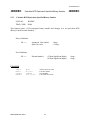
1-1. CPU32Bug Operation Mode Flow Diagram ...................................................................... 1-2
1-2. BCC Memory Map ............................................................................................................. 1-6
LIST OF TABLES
TABLES
2-1.
2-2.
3-1.
4-1.
5-1.
6-1.
6-2.
B-1.
C-1.
C-2.
C-3.
C-4.
C-5.
C-6.
PAGE
Debugger Address Parameter Format................................................................................. 2-5
CPU32Bug Exception Vectors ........................................................................................... 2-8
Debug Monitor Commands ................................................................................................ 3-1
CPU32Bug Assembler Addressing Modes......................................................................... 4-7
CPU32Bug System Call Routines ...................................................................................... 5-3
MCU CPU Diagnostic Tests............................................................................................... 6-6
Memory Diagnostic Tests................................................................................................. 6-11
Self-Test Error Messages....................................................................................................B-1
CPU32Bug Customization Area.........................................................................................C-5
MCU SCI Communication Formats .................................................................................C-14
Rev. A Chip Selection Summary......................................................................................C-15
Rev. B Chip Selection Summary ......................................................................................C-16
BCC Rev. C Chip Selection Summary .............................................................................C-17
PFB Rev. C Compatibility................................................................................................C-18
M68CPU32BUG/D REV 1
vi
GENERAL INFORMATION
CHAPTER 1
GENERAL INFORMATION
1.1 INTRODUCTION
This chapter provides a general description, installation instructions, start-up and system restart
instructions, memory requirements, and a terminal input/output (I/O) control description for the
M68CPU32BUG Debug Monitor (hereafter referred to as CPU32Bug). Information in this
manual covers the 1.00 version of the CPU32Bug.
1.2 GENERAL DESCRIPTION
The CPU32Bug package evaluates and debugs systems built around the M6833XBCC Business
Card Computer. System evaluation facilities are available for loading and executing user
programs. Various CPU32Bug routines that handle I/O, data conversion, and string functions are
available to user programs through the TRAP #15 handler.
CPU32Bug includes:
•
Commands for display and modification of memory,
•
Breakpoint capabilities,
•
An assembler/disassembler useful for patching programs,
•
A power-up self test feature which verifies system integrity,
•
A command-driven user-interactive software debugger (the debugger), and
•
A user interface which accepts commands from the system console terminal.
There are two modes of operation in the CPU32Bug monitor; the debugger mode and the
diagnostic mode. When the user is in the debugger directory the prompt CPU32Bug> is
displayed, and the user has access to the debugger commands (see Chapter 3). When the user is
in the diagnostic mode the prompt CPU32Diag> is displayed, and the user has access to the
diagnostic commands (see Chapter 6). These modes are also called directories.
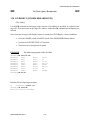
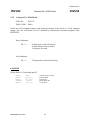
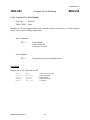
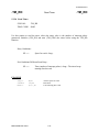
CPU32Bug is command-driven. It performs various operations in response to user commands
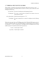
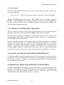
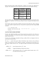
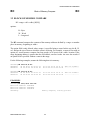
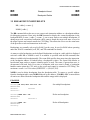
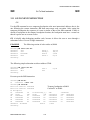
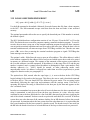
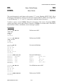
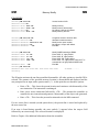
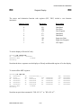
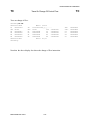
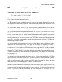
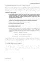
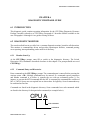
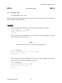
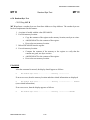
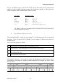
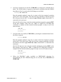
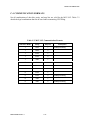
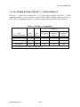
entered at the keyboard. Figure 1-1 illustrates the flow of control in CPU32Bug. CPU32Bug
executes entered commands and the prompt reappears upon completion. However, if a command
is entered which causes execution of user target code (i.e., GO) then control may or may not
return to CPU32Bug. This depends upon the user program function.
CPU32Bug is similar to Motorola’s other debugging packages, but there are two noticeable
differences. Many of the commands are more flexible with enhanced functionality. And the
debugger has more detailed error messages and an expanded on-line help facility.
M68CPU32BUG/D REV 1
1-1
GENERAL INFORMATION
MAIN
POWER-UP/RESET
DISPLAY BUG PROMPT
WAIT FOR INPUT
NO
WARM START?
YES
DOES COMMAND
CAUSE TARGET CODE
EXECUTION
SET DEBUGGER
DIRECTORY
NO
YES
RESTORE
TARGET STATE
EXECUTE COMMAND
DISPLAY DEBUGGER
NAME AND VERSION
TARGET CODE
GO TO MAIN
INITILIZE BUG VARIBLES
DISPLAY WARM
START MESSAGE
RUN SYSTEM
CONFIDENCE TEST
EXECPTION
EXCEPTION
HANDLERS
SET DEBUGGER
DIRECTORY
SAVE TARGET
STATE
DISPLAY DEBUGGER NAME & VERSION
DISPLAY RESULTS OF CONFIDENCE
TEST
DISPLAY TARGET
REGISTERS
GO TO MAIN
Figure 1-1. CPU32Bug Operation Mode Flow Diagram
M68CPU32BUG/D REV 1
1-2
GENERAL INFORMATION
1.3 USING THIS MANUAL
Those users unfamiliar with debugging packages should read Chapter 1 before attempting to use
CPU32Bug. This provides information about CPU32Bug structure and capabilities.
Paragraph 1.4 Installation and Start-up describes a step-by-step procedure for powering up the
module and obtaining the CPU32Bug prompt on the terminal screen.
For questions about syntax or operation of a particular CPU32Bug command, turn to the
paragraph which describes that particular command in Chapter 3.
Some debugger commands take advantage of the built-in one-line assembler/disassembler. The
command descriptions in Chapter 3 assume that the user is familiar with the
assembler/disassembler functionality. Chapter 4 includes a description of the assembler/
disassembler.
NOTE
In the examples shown, all user inputs are given in bold text. This should clarify
the examples by distinguishing between character input by the user and character
output by CPU32Bug. The symbol <CR> represents the carriage return key on the
user’s terminal keyboard. Whenever this symbol appears it indicates a carriage
return should be entered by the user.
1.4 INSTALLATION AND START-UP
Use the following set-up procedure to enable CPU32Bug to operate with the BCC:
1. Configure the jumpers on the BCC module. Refer to the EVK User’s Manual
Motorola publication number M68332EVK/AD1 or M68331EVK/AD1.
2. Connect the DB-9 serial communication cable connector to the terminal or host
computer which is to be the CPU32Bug system console. Connect the other end of the
cable to P4 on the BCC.
Set up the terminal as follows:
•
Eight bits per character
•
One stop bit per character
•
Parity disable
•
9600 baud rate
M68CPU32BUG/D REV 1
1-3
GENERAL INFORMATION
NOTE
In order for high-baud rate serial communication between
CPU32Bug and the terminal to function properly, the terminal
must use XON/XOFF handshaking. If messages are garbled and
have missing characters, check the terminal to verify XON/XOFF
handshaking is enabled.
3. Power up the system. CPU32Bug executes a self-test and displays the sign on
message (which includes version number) and the debugger prompt CPU32Bug>.
1.5 SYSTEM RESTART
There are three ways to initialize the system to a known state. Each situation determines the
appropriate system restart technique.
1.5.1 Reset
The M68300PFB platform board reset switch returns the system to a known state. When the reset
switch is first pushed the MCU send the default XON character to the terminal to prevent
possible terminal lockup. There are two reset modes: COLD and WARM. COLD reset is the
CPU32Bug default, refer to the RESET command description. During COLD reset a total
system initialization occurs, similar to the BCC power-up sequence. All static variables are
restored to their default states. The serial port is reset to its default state. The breakpoint table is
cleared. The offset registers are cleared. The target registers are invalidated. Input and output
character queues are cleared. On-board devices (timer, serial ports, etc) are reset. During WARM
reset, CPU32Bug variables and tables are preserved, as well as the target state registers and
breakpoints.
Use reset if the processor halts, for example, after a halt monitor fault, or if the CPU32Bug
environment is lost (vector table is destroyed, etc).
1.5.2 Abort
The M68300PFB platform board abort switch terminates all in-process instructions. When abort
is executed while running target code, a snapshot of the processor state is captured and stored in
the target registers. For this reason abort is appropriate when terminating a user program that is
being debugged. Use abort to regain control if the program gets caught in a loop, etc. The target
PC, stack pointers, etc. help pinpoint malfunctions.
Abort generates a non-maskable, level-seven interrupt. The target registers reflect the machine
state at the time of an abort and are displayed on the display screen. Any breakpoints installed in
the user code are removed and the breakpoint table remains intact. Control is then returned to the
debugger.
M68CPU32BUG/D REV 1
1-4
GENERAL INFORMATION
1.5.3 Break
The BREAK key on the terminal keyboard initiates a break. Break does not generate an
interrupt. The only time break is recognized is when characters are sent or received by the
debugger console. Break removes any breakpoints in the user code and keeps the breakpoint table
intact. Break does not, however, take a snapshot of the machine state nor does it display the
target registers. It is useful for terminating active debugger commands that are outputing large
blocks of data.
NOTE
When using terminal emulation programs such as ProComm or
Kermit, the BREAK key on the keyboard is local to the emulation
program and may not be transmitted to the BCC. Consult your
emulation program’s user manual for the procedure on sending a
BREAK signal to the port connected to the BCC.
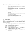
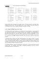
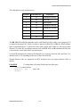
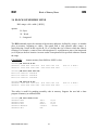
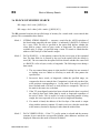
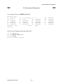
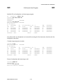
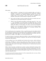
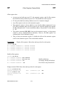
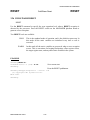
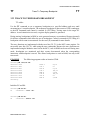
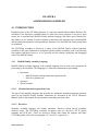
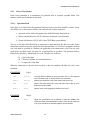
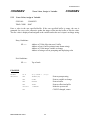
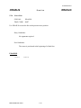
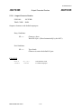
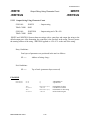
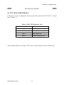
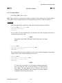
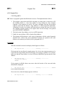
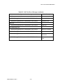
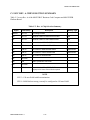
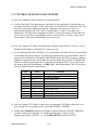
1.6 MEMORY REQUIREMENTS
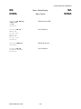
The program portion of CPU32Bug is approximately 64k bytes of code. The EPROM on-board
the BCC contains 128k bytes and is mapped at locations $E0000 to $FFFFF. However, the
CPU32Bug code is position-independent and can execute anywhere in memory. The second half
of the EPROM ($F0000 - $FFFFF) is blank and available for user programs. See Appendix C
CPU32Bug Customization.
CPU32Bug requires a minimum of 12k bytes of random access memory (RAM) to operate. This
memory may be either off-board system memory (i.e., on an external memory board) or BCC onboard RAM. On-board RAM allows stand-alone operation of the BCC.
The first 12k bytes are used for CPU32Bug stack and static variable space and the rest of
memory is reserved as user space. Whenever the BCC is reset, the target program counter is
initialized to the beginning user space address and the target stack pointers are initialized to
addresses at the end of the user space. The target instruction stack pointer (SSP) is set to the top
of the user space. Register initialization is done solely as a convenience for the user. Consult the
CPU32 Reference Manual for information regarding actual register values during a poweron/reset.
M68CPU32BUG/D REV 1
1-5
GENERAL INFORMATION
XXX7FF(2)
INTERNAL RAM(1)
XXX000
FFFFFF
MCU
INTERNAL
MODULES
FFF000
OPTIONAL FPCP(3)
PFB(4): U5
FFE800
800000
ALTERNATE MCU
INTERNAL MODULES
LOCATION
(see APPENDIX C)
7FF000
OPTIONAL RAM/EPROM
PFB: U2 & U4
CPU32BUG EPROM
BCC: U4
OPTIONAL RAM
PFB: U1 & U3
TARGET RAM
BCC: U2 & U3
SYSTEM RAM
BCC: U2 & U3
110000 /120000(5)
100000
0E0000
CPU32BUG
STACK
020000
CPU32BUG
INTERNAL
VARIABLES
CPU32BUG VECTOR
TABLE
010000
003000
TARGET VECTOR
TABLE
000000
(1) Consult the MCU device User’s Manual.
(2) XXXBase address is user programmable. Internal MCU modules,
such as internal RAM, can be configured on power-up/reset by
using the Initialization Table (INITTBL) covered in Appendix C.
(3) Floating Point Coprocessor - MC68881/MC68882
(4) Platform Board
(5) Depends on the memory device type used.
Figure 1-2. BCC Memory Map
M68CPU32BUG/D REV 1
1-6
GENERAL INFORMATION
1.7 TERMINAL INPUT/OUTPUT CONTROL
When entering a command at the prompt, the following control codes may have a caret, " ^ ",
preceding the character, this indicates that the Control or CTRL key must be held down while
striking the character key).
^X (Cancel line) The cursor is backspaced to the beginning of the line.
^H (backspace) The cursor is moved back one position. The character at the new
cursor position is erased.
<del> (delete/rubout) Performs the same function as ’’^H’’.
^D (redisplay) The entire command line as entered is redisplayed on the following
line.
When observing output from any CPU32Bug command, the XON and XOFF characters may be
entered to control the output, if the XON/XOFF protocol is enabled (default). These characters
are initialized to ’’^S’’ and ’’^Q’’ respectively by CPU32Bug, but may be changed by the user using
the PF command. The initialized (default) mode operations are:
^S (wait) Console output is halted.
^Q (resume) Console output is resumed.
M68CPU32BUG/D REV 1
1-7
GENERAL INFORMATION
M68CPU32BUG/D REV 1
1-8
DEBUG MONITOR DESCRIPTION
CHAPTER 2
DEBUG MONITOR DESCRIPTION
2.1 INTRODUCTION
CPU32Bug performs various operations in response to user commands entered at the keyboard.
When the debugger prompt CPU32Bug> appears on the terminal screen the debugger is ready to
accept commands.
2.2 ENTERING DEBUGGER COMMAND LINES
As the command line is entered it is stored in an internal buffer. Execution begins only after the
carriage return is entered. This allows the user to correct entry errors using the control characters
described in paragraph 1.7.
The debugger executes commands and returns the CPU32Bug> prompt. However, if the entered
command causes execution of user target code, (i.e., GO), then control may or may not return to
the debugger. This depends upon the user program function. For example, if a breakpoint is
specified, then control returns to the debugger when the breakpoint is encountered. The user
program also returns control to the debugger by means of the TRAP #15 function, RETURN
(described in paragraph 5.2.16). Also refer to the paragraphs in Chapter 3 which detail elements
of the GO commands.
In general debugger commands include:
•
A command identifier (i.e., MD or md for the memory display command). Both
upper- or lower-case characters are allowed for command identifiers and options.
•
At least one intervening space before the first argument.
•
A port number for running with multiple ports.
•
Any required arguments, as specified by command.
•
An option field, set off by a semicolon (;) to specify conditions other than the default
conditions of the command.
•
Some commands (MD, GO, T, etc) are repeatable, i.e., entering a carriage return
(<CR>) only causes the last command to be repeated and the address (<ADDR>), if
any, incremented. Thus after an MD command, sequential memory locations will be
displayed by entering a carriage return only. Or after entering a TRACE (T)
command, entering a carriage return (<CR>) only traces the next instruction.
•
Multiple debugger commands may be entered on a single command line by separating
the commands with the explanation point (!) character.
M68CPU32BUG/D REV 1
2-1
DEBUG MONITOR DESCRIPTION
The commands use a modified Backus-Naur syntax. The meta-symbols are:
<>
The angular brackets enclose a symbol, known as a syntactic variable. The
syntactic variable is replaced in a command line by one of a class of
symbols it represents.
[]
Square brackets enclose an optional symbol. The enclosed symbol may
occur zero or one time. In some cases, where noted, square brackets are
required characters.
[]...
Square brackets followed by periods enclose a symbol that is
optional/repetitive. The symbol within the brackets may appear zero or
more times.
|
This symbol indicates that a choice is to be made. Select one of several
symbols separated by a straight line.
/
Select one or more of the symbols separated by the slash.
{}
2.2.1
Brackets enclose optional symbols that may occur zero or more times.
Syntactic Variables
The following syntactic variables are used in the command descriptions which follow. In
addition, other syntactic variables may be used and are defined in the particular command
description in which they occur.
<DEL>
<ADDR>
Delimiter; either a comma or a space. <EXP> - Expression (described in
detail in paragraph 2.2.1.1).
Address (described in detail in paragraph 2.2.1.2).
<COUNT>
Count; the same syntax as < EXP> .
<RANGE>
A range of memory addresses which may be specified either by <
ADDR><DEL><ADDR> or by <ADDR> :<COUNT> .
<TEXT>
An ASCII string of as many as 255 characters, delimited with single quote
marks (’TEXT’).
M68CPU32BUG/D REV 1
2-2
DEBUG MONITOR DESCRIPTION
2.2.1.1 Expression as a Parameter
An expression is one or more numeric values separated by the arithmetic operators:
+ plus
–
minus
*
multiplied by
/
divided by
& logical AND
<< shift left
>> shift right
Base identifiers define numeric values as either a hexadecimal, decimal, octal or binary number.
Base
Identifier
Examples
Hexadecimal
$
$FFFFFFFF
Decimal
&
&1974, &10-&4
Octal
@
@456
Binary
%
%1000110
If no base identifier is specified, then the numeric value is assumed to be hexadecimal.
A numeric value may also be expressed as a string literal of as many as four characters. The
string literal must begin and end with single quote marks ('). The numeric value is interpreted as
the concatenation of the ASCII values of the characters. This value is right-justified, as is any
other numeric value.
String Literal
Numeric Value (in hex)
’A’
41
’ABC’
414243
’TEST’
54455354
Evaluation of an expression is always from left to right unless parentheses are used to group part
of the expression. There is no operator precedence. Sub-expressions within parentheses are
evaluated first. Nested parenthetical sub-expressions are evaluated from the inside out.
M68CPU32BUG/D REV 1
2-3
DEBUG MONITOR DESCRIPTION
EXAMPLES
Valid expressions.
Expression
Result (in hex)
FF0011
FF0011
45+99
DE
&45+&99
90
@35+@67+@10
5C
%10011110+%1001
A7
88<<10
00880000
AA&F0
A0
The total value of the expression must be between 0 and $FFFFFFFF.
2.2.1.2 Address as a Parameter
Many commands use <ADDR> as a parameter. The syntax accepted by CPU32Bug is similar to
the one accepted by the MC68300 Family one-line assembler. All control addressing modes are
allowed. An address+offset register mode is also allowed.
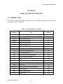
Table 2-1 summarizes the address formats which are acceptable for address parameters in
debugger command lines.
M68CPU32BUG/D REV 1
2-4
DEBUG MONITOR DESCRIPTION
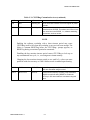
Table 2-1. Debugger Address Parameter Format
Format
Example
Description
N
140
Absolute address+contents of automatic offset register.
N+Rn
332+R5
Absolute address+contents of the specified offset register (not an
assembler-accepted syntax).
(An)
(A1)
Address register indirect.
(d,An)
or
d(An)
(120,A1)
120(A1)
Address register indirect with displacement (two formats accepted).
(d,An,Xn)
or
d(An,Xn)
(&120,A1,D2)
&120(A1,D2)
Address register indirect with index and displacement (two formats
accepted).
Symbol Definition
N - Absolute address (any valid expression)
Dn - Data register n
An - Address register n
Xn - Index register n (An or Dn) d Displacement (any valid expression)
bd - Base displacement (any valid expression) n Register number (0 to 7)
Rn - Offset register n
ZXn - Zero suppressed register Xn
2.2.1.3 Offset Registers
Eight pseudo-registers (R0 through R7) called offset registers are used to simplify the debugging
of re-locatable and position-independent files. These files when listed have a starting address
(normally 0), but when loaded into memory, due to the offset registers, they are loaded into a
different memory location. Implementing offset registers makes it harder to correlate addresses in
the listing with addresses in the loaded program. The offset registers solve this problem by taking
into account this difference and forcing the display of addresses in a relative address+offset
format. The range for each offset register is set by two addresses: base and top. Specifying the
base and top addresses for an offset register sets its range. Offset registers have adjustable ranges
which may overlap. In the event that an address falls in two or more offset register ranges, the
one that yields the least offset is chosen.
NOTE
Relative addresses are limited to 1 megabyte (5 digits), regardless
of the range of the closest offset register.
M68CPU32BUG/D REV 1
2-5
DEBUG MONITOR DESCRIPTION
EXAMPLE
1
2
3
4
5
6
7
8
9
10
11
12
13
14
******
******
A portion of the listing file of a re-locatable module assembled with the
MC68300 Family DOS resident assembler is shown below:
0
0
0
0
0
0
0
0
00000000
00000004
00000006
00000008
0000000A
0000000C
00000010
00000014
48E78080
4280
1018
5340
12D8
51 C8FFFC
4CDF0101
*
* MOVE STRING SUBROUTINE
*
MOVESTR MOVEM.L
D0/A0,-(A7)
CLR.L
D0
MOVE.B
(A0)+,D0
SUBQ.W
#1,D0
LOOP
MOVE.B
(A0)+,(A1)+
MOVS
DBRA
D0,LOOP
MOVEM.L
(A7)+,D0/A0
RTS
END
TOTAL ERRORS 0TOTAL WARNINGS
0-
The above program was loaded at address 0000427C. The disassembled code is:
CPU32Bug>MD 427C;DI<CR>
0000427C 48E78080
00004280 4280
00004282 1018
00004284 5340
00004286 12D8
00004288 51C8FFFC
0000428C 4CDF0101
00004290 4E75
MOVEM.L
CLR.L
MOVE.B
SUBQ.W
MOVE.B
DBF
MOVEM.L
RTS
D0/A0,-(A7)
D0
(A0)+,D0
#1,D0
(A0)+,(A1)+
D0,$4286
(A7)+,D0/Ao
By using one of the offset registers, the disassembled code address can be made to match the
listing file address as follows:
CPU32Bug>OF R0<CR>
R0 =00000000 00000000? 427C: 16.<CR>
CPU32Bug>MD 0+R0;DI<CR>
00000+R0 48E78080
MOVEM.L
D0/A0,-(A7)
00004+R0 4280
CLR.L
D0
00006+R0 1018
MOVE.B
(A0)+,D0
00008+R0 5340
SUBQ.W
#1,D0
0000A+R0 12D8
MOVE.B
(A0)+,(A1)+
0000C+R0 51C8FFFC
DBF
D0,$A+R0
00010+R0 4CDF0101
MOVEM.L
(A7)+,D0/A0
00014+R0 4E75
RTS
CPU32Bug>
For Additional information about the offset registers, see the OF command description.
M68CPU32BUG/D REV 1
2-6
DEBUG MONITOR DESCRIPTION
2.2.2 Port Numbers
Some CPU32Bug commands allow the user to decide which port is the input or output port.
Valid port numbers are:
0 - MCU SCI Port
(RS-232C communication port; P4 on the BCC and P9 on the PFB)
Although CPU32Bug supports other ports (see PF command), there is no hardware present on
the BCC to support additional ports. Thus the commands which allow port numbers (DU, LO,
PF, VE) can only use port 0. Those commands requiring a second port (PA, TM) are not
functional without additional hardware.
2.3 ENTERING AND DEBUGGING PROGRAMS
There are various ways to enter a user program into system memory. One is to create the program
using the assembler/disassembler option and the MM (memory modify) command.
The user enters the program one source line at a time. After each source line is entered, it is
assembled and the object code is loaded into memory. Refer to Chapter 4 for complete details of
the CPU32Bug assembler/disassembler.
Another way to enter a program is to download an object file from a host system (i.e., a personal
computer). The program must be in S-record format (described in Appendix A) and may be
assembled or compiled on the host system. The file is downloaded from the host into BCC
memory via the debugger LO command. Alternately, the program may be created using the
CPU32Bug MM command as outlined above and stored to the host using the DU (dump)
command. A communication link must exist between the host system and the BCC’s serial port.
2.4 CALLING SYSTEM UTILITIES FROM USER PROGRAMS
A convenient method to input and output characters as well as many other useful operations is
provided by the TRAP #15 instructions. This frees the user from having to write these routines
into the target code. Refer to Chapter 5 for details on various TRAP #15 utilities and how to
execute them from a user program.
2.5 PRESERVING DEBUGGER OPERATING ENVIRONMENT
Avoiding contamination of the debugger operating environment is explained in the following
paragraphs. CPU32Bug uses certain MCU on-board resources and may also use off-board system
memory to store temporary variables, exception vectors, etc. If the user violates CPU32Bug
dependent memory space, then the debugger may not function.
M68CPU32BUG/D REV 1
2-7
DEBUG MONITOR DESCRIPTION
2.5.1 CPU32Bug Vector Table and Workspace
CPU32Bug requires 12k bytes of RAM to operate. On power-up or reset, CPU32Bug allocates
this memory space. The first 1024-bytes are reserved as a user program vector table area and the
second 1024-bytes are reserved as an exception vector table for use by the debugger. Next,
CPU32Bug reserves space for static variables and initializes these variables to predefined default
values. After the static variables, CPU32Bug allocates space for the system stack, then initializes
the system stack pointer to the top of this area.
With the exception of the first 1024-byte vector table area, do not to use the above-mentioned
reserved memory areas. Refer to paragraph 1.6 to define the reserved memory area location. If,
for example, a user program inadvertently wrote over the static variable area containing the serial
communication parameters, these parameters would be lost, resulting in a loss of communication
with the system terminal. If a user program corrupts the system stack, then an incorrect value
may be loaded into the processor’s counter, causing the system to crash.
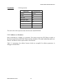
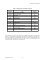
2.5.2 CPU32Bug Exception Vectors
The debugger exception vectors are listed below. Do not change these specified vector offsets in
the target program vector table or the associated debugger facilities (breakpoints, trace mode,
etc.) will not operate.
Table 2-2. CPU32Bug Exception Vectors
Vector
Number
Offset
Exception
CPU32bug Facility
4
$10
Illegal
Instruction breakpoints (Used instruction by GO, GN,
GT)
9
$24
Trace
T. TC, TT
31
$7C
Level 7 interrupt
ABORT push-button
47
$BC
TRAP #15
System calls (see Chapter 5)
66
$108
User Defined
Timer Trap #15 Calls ($4X)
When the debugger handles one of the exceptions listed in Table 2-2, the target stack pointer is
left pointing past the bottom of the exception stack frame; that is, it reflects the system stack
pointer values just before the exception occurred. In this way, the operation of the debugger
facility (through an exception) is transparent to the user, but it does change the locations on the
stack.
M68CPU32BUG/D REV 1
2-8
DEBUG MONITOR DESCRIPTION
EXAMPLE
Trace one instruction using debugger.
CPU32Bug>RD<CR>
PC
=00003000
SR
SFC =5=SD
DFC
D0
=00000000
D1
D4
=00000000
D5
A0
=00000000
A1
A4
=00000000
A5
00003000 203900100000
CPU32Bug>T<CR>
PC
=00003006
SFC =5=SD
D0
=12345678
D4
=00000000
A0
=00000000
A4
=00000000
00003006 D280
CPU32Bug>
=2700=TR:OFF_S_7_.....
=5=SD
USP =00003830
=00000000
D2
=00000000
=00000000
D6
=00000000
=00000000
A2
=00000000
=00000000
A6
=00000000
MOVE.L ($100000).L,D0
SR
=2700=TR:OFF_S_7_.....
DFC =5=SD
USP =00003830
D1
=00000000
D2
=00000000
D5
=00000000
D6
=00000000
A1
=00000000
A2
=00000000
A5
=00000000
A6
=00000000
ADD.L
D0,D1
VBR
SSP*
D3
D7
A3
A7
=00000000
=00004000
=00000000
=00000000
=00000000
=00004000
VBR
SSP*
D3
D7
A3
A7
=00000000
=00004000
=00000000
=00000000
=00000000
=00004000
Notice that the value of the target stack pointer register (A7) has not changed even though a trace
exception has taken place. The user program may use the exception vector table provided by
CPU32Bug or it may create a separate exception vector table of its own.
2.5.2.1 Using CPU32Bug Target Vector Table
CPU32Bug initializes and maintains a vector table area for target programs. A target program is
any user program started by the CPU32Bug with GO or Trace commands. The starting address of
this target-vector table area is the base address of the BCC, described in paragraph 1.6. This
address is loaded into the target-state-vector base register at power-up or during a cold-start reset.
For verification use the RD command immediately after power-up to display the target-state
registers.
CPU32Bug loads the target-vector table with the debugger vectors (listed in Table 2-2) and the
other vector locations with the address of a generalized exception handler (refer to paragraph
2.5.2.3). The target program allocates as many vectors as required by simply writing its own
exception vectors into the table. If the vector locations listed in Table 2-2 are over-written, then
the accompanying debugger functions will be lost.
CPU32Bug maintains a separate vector table for its own use in a 1k byte space in the reserved
memory space. The debugger vector table is completely transparent to the user and no
modifications should ever be made to it.
M68CPU32BUG/D REV 1
2-9
DEBUG MONITOR DESCRIPTION
2.5.2.2 Creating Vector Tables
A user program may create a separate vector table to store its exception vectors. If this is done,
the user program must change the value of the vector base register to point to the new vector
table. To use the debugger facilities, copy the vectors from the CPU32Bug vector table into the
corresponding user vector table locations (block of memory move (BM) command).
The vector for the CPU32Bug generalized exception handler (described in detail in paragraph
2.5.2.3) may be copied from offset $08 (Bus Error vector) in the target-vector table to all
locations in the user’s vector table where a separate exception handler is not used. This provides
diagnostic support in the event execution of the user program is terminated by an unexpected
exception. The generalized exception handler gives a formatted display of the target registers and
identifies the type of the exception.
The following is an example of a user routine which builds a separate vector table and then sets
the vector base register to point at it.
*
***
BUILDX – Build
*
BUILDX
MOVEC.L
LEA
MOVE.L
MOVE.W
LOOP
MOVE.L
SU BQ.W
BPL.B
MOVE.L
MOVE.L
MOVE.L
LEA.L
MOVE.L
MOVEC.L
RTS
END
exception vector table ***
VBR,A0
$1 0000,A1
$8(A0),D0
$3FC,D1
D0,(A1,D1)
#4, D 1
LOOP
$1 0(A0),$1 0(A1 )
$24(A0),$24(A1 )
$BC(A0),$BC(A1 )
TIMER(PC),A2
A2,$2C(A1 )
A1 ,VBR
Get copy of VBR.
New vectors at $10000.
Get generalized exception vector.
Load count (all vectors).
Store generalized exception vector.
Initialize entire vector table.
Copy breakpoints vector.
Copy trace vector.
Copy system call vector.
Get user exception vector.
Install as F-Line handler.
Change VBR to new table.
The user program may use one or more of the exception vectors that are required for debugger
operation if the user’s exception handler can determine when to handle the exception itself and
when to pass the exception to the debugger.
When an exception occurs which requires debugger operation (i.e., ABORT), the user’s
exception handler must read the vector offset from the exception-stack-frame format word. This
offset is added to the address of the CPU32Bug target program vector table (which the user
program saves), producing the address of the CPU32Bug exception vector. The user program
then jumps to the address stored at this vector location (i.e., which is the address of the
CPU32Bug exception handler).
The user program must ensure an exception stack frame is in the stack and that it is identical to
one the processor would create for the particular exception. It may then jump to the address of
the exception handler.
M68CPU32BUG/D REV 1
2-10
DEBUG MONITOR DESCRIPTION
EXAMPLE
The user exception handler passes an exception along to the debugger.
*
*** EXCEPT - Exception handler ****
*
EXCEPT
SUBQ.L
LINK
MOVEM.L
#4,A7
A6,#0
A0-A5/D0-D7,-(A7)
Save space in stack for a PC value.
Frame pointer for accessing PC space.
Save registers.
: decide here if user code will handle exception, if so, branch...
MOVE.L
MOVE.W
AND.W
MOVE.L
UNLK
RTS
BUFVBR,A0
14(A6), Do
#$0FFF,D0
(A0,D0.W),4(A6)
Pass exception to debugger; Get VBR.
Get the vector offset from stack frame.
Mask off the format information.
Store address of debugger exception handler.
A6
Put address of exception handler into PC and go.
2.5.2.3 CPU32Bug Generalized Exception Handler
The CPU32Bug generalized exception handler supervises all exceptions not listed in Table 2-2.
For these exceptions, the target stack pointer points to the top of the user exception stack frame.
In this way, if an unexpected exception occurs during user code segment execution, the exception
stack frame displays to assist in determining the cause of the exception.
EXAMPLE
Bus error at address $F00000. It is assumed for this example that an access
of memory location $F00000 initiates bus error exception processing.
CPU32Bug>RD<CR>
PC
=00003000
SR
=2700=TR:OFF_S_7_....
VBR =00000000
SFC =5=SD
DFC =5=SD
USP =0000FC00
SSP* =00004000
D0
=00000000
D1
=00000000
D2
=00000000
D3
=00000000
D4
=00000000
D5
=00000000
D6
=00000000
D7
=00000000
A0
=00000000
A1
=00000000
A2
=00000000
A3
=00000000
A4
=00000000
A5
=00000000
A6
=00000000
A7
=00004000
00003000 203900F0
0000
MOVE.L
($F00000).L,D0
CPU32Bug>T<CR>
Exception: Bus Error
Format/Vector=C008
SSW=0065 Fault Addr.=00F00000 Data=FFFF3000 Cur. PC=00003000 Cnt. Reg.=0001
PC
=00003000
SR
=A700=TR:ALL_S_7_....
VBR =00000000
SFC =5=SD
DFC =5=SD
USP =0000FC00
SSP* =00003FE8
D0
=00000000
D1
=00000000
D2
=00000000
D3
=00000000
D4
=00000000
D5
=00000000
D6
=00000000
D7
=00000000
A0
=00000000
A1
=00000000
A2
=00000000
A3
=00000000
A4
=00000000
A5
=00000000
A6
=00000000
A7
=00003FE8
00003000 203900F0
0000
MOVE.L
($F00000).L,D0
CPU32Bug>
M68CPU32BUG/D REV 1
2-11
DEBUG MONITOR DESCRIPTION
Before the normal register display information is printed, the exception type information is
displayed. This includes the type of exception with its format/vector word and the following:
Mnemonic
Description
Offset
SSW
Special Status Word
+$16
Fault Addr.
Faulted Address
+$10
Data
Data
+$0C
Cur. PC
Program Counter
+$02
Cnt. Reg.
Internal Transfer
Count Register
+$14
The upper nibble of the count register (Cnt. Reg.) contains the microcode revision number of the
MCU device. Consult the CPU32 Reference Manual, Section 6 Exception Processing for more
details.
Notice that the target stack pointer is different. The target stack pointer now points to the last
value of the stacked exception stack frame. Examine the exception stack frame using the MD
command.
CPU32Bug>MD (A7):C<CR>
00003FE8 A700 0000 3000 C008
00003FF8 0000 3000 0001 0065
CPU32Bug>
00F0 0000 FFFF 3000
‘...0.@ p....0.
..0....e
2.6 FUNCTION CODE SUPPORT
Function codes identify the address space being accessed on any given bus cycle, and are an
extension of the address. The function codes provide additional information required to find the
proper memory location.
For this reason, all debugger commands involving an address field were changed to allow the
specification of function codes:
The caret ( ^ ) symbol following the address field indicates that a function code specification
follows. The function code can be entered by specifying a valid function code mnemonic or by
specifying a number between 0 and 7. The syntax for address and function code specifications
are:
<ADDR>^<FC>
<ADDR>^^
<ADDR>^<FC>=
M68CPU32BUG/D REV 1
Sets the function code to <FC> value.
Toggles the displaying of function code values.
Sets the function code to <FC> and the default function code to <FC>.
The default value at power up is SD.
2-12
DEBUG MONITOR DESCRIPTION
The valid function code mnemonics are:
Function
Code Mnemonic
Description
0
F0
Unassigned, reserved
1
UD
User Data
2
UP
User Program
3
F3
Unassigned, reserved
4
F4
Unassigned, reserved
5
SD
Supervisor Data
6
SP
Supervisor Program
7
CS
CPU Space Cycle
The BR, GD, GO, and GT commands set the valid function codes to either a user program (UP)
or supervisor program (SP). When execution is started via GO, GN, or GD, the default address
space is determined by bit 13 (the S-bit) of the status register (SR). When set, SP is used; when
cleared, UP is used. By specifying a function code with GO, GT, or GD command, the SR S-bit
is forced to the correct state before execution begins.
For the GT command, the temporary breakpoint is set using the function code specified, or it
defaults to SP or UP, depending on the state of the S-bit in the SR.
Though function codes are supported, the BCC hardware does not require function codes to
operate.
EXAMPLE
To change data at location $5000 in the user data space.
CPU32Bug>m 5000^ud<CR>
00005000^UD
0000
?
CPU32Bug>
M68CPU32BUG/D REV 1
1234.<CR>
2-13
DEBUG MONITOR DESCRIPTION
M68CPU32BUG/D REV 1
2-14
DEBUG MONITOR COMMANDS
CHAPTER 3
DEBUG MONITOR COMMANDS
3.1 INTRODUCTION
This chapter contains descriptions and examples of the CPU32Bug debugger commands. Table
3-1 summarizes these commands.
Table 3-1. Debug Monitor Commands
Command
Mnemonic
Title
Paragraph
BC
Block of Memory Compare
3.2
BF
Block of Memory Fill
3.3
BM
Block of Memory Move
3.4
BR/NOBR
Breakpoint Insert/Delete
3.5
BS
Block of Memory Search
3.6
BV
Block of Memory Verify
3.7
DC
Data Conversion
3.8
DU
Dump S-Records
3.9
GD
Go Direct (Ignore Breakpoints)
3.10
GN
Go to Next Instruction
3.11
GO
Go Execute User Program (alias G)
3.12
GT
Go To Temporary Breakpoint
3.13
HE
Help
3.14
LO
Load S-Records from Host
3.15
Macro Define/Display/Delete
3.16
Macro Edit
3.17
Macro Expansion Listing Enable/Disable
3.18
MD
Memory Display
3.19
MM
Memory Modify (alias M)
3.20
MS
Memory Set
3.21
MA/NOMA
MAE
MAL/NOMAL
M68CPU32BUG/D REV 1
3-1
DEBUG MONITOR COMMANDS
Table 3-1. Debug Monitor Commands (continued)
Command
Mnemonic
OF
Title
Paragraph
Offset Registers Display/Modify
3.22
Printer Attach/Detach
3.23
PF
Port Format
3.24
RD
Register Display
3.25
Cold/Warm Reset
3.26
RM
Register Modify
3.27
RS
Register Set
3.28
SD
Switch Directories
3.29
Trace
3.30
TC
Trace On Change of Control Flow
3.31
TM
Transparent Mode
3.32
TT
Trace To Temporary Breakpoint
3.33
VE
Verify S-Records Against Memory
3.34
PA/NOPA
RESET
T
Each command is described in the following text. Command syntax symbols are explained in
section 2.1. In the examples of the debugger commands all user inputs are in bold type. This
helps clarify examples by distinguishing user input characters from CPU32Bug output characters.
The symbol <CR> represents the carriage return key on the user’s terminal keyboard. This
symbol indicates the user should enter a carriage return.
M68CPU32BUG/D REV 1
3-2
DEBUG MONITOR COMMANDS
BC
BC
Block of Memory Compare
3.2 BLOCK OF MEMORY COMPARE
BC <range><del><addr>[;B|W|L]
options:
B – Byte
W – Word
L – Longword
The BC command compares the contents of the memory addresses defined by <range> to another
place in memory, beginning at <addr>.
The option field is only allowed when <range> is specified using a count. In this case, the B, W,
or L defines the size of data to which the count is referring. For example, a count of four with an
option of L would mean to compare four long words (or 16 bytes) to the <addr> location. If the
range beginning address is greater than the end address, an error results. An error also results if
an option field is specified without a count in the range.
For the following examples, assume the following data is in memory.
CPU32Bug>MD 4000:20;B<CR>
00004000
54 48 49 53 20 49 53 20
00004010
00 00 00 00 00 00 00 00
41 20 54 45 53 54 21 21
00 00 00 00 00 00 00 00
THIS IS A TEST!!
................
CPU32Bug>MD 4100:20;B<CR>
00004100
54 48 49 53 20 49 53 20
00004110
00 00 00 00 00 00 00 00
41 20 54 45 53 54 21 21
00 00 00 00 00 00 00 00
THIS IS A TEST!!
................
EXAMPLES
CPU32Bug>BC 4000,401F 4100<CR>
Effective address: 00004000
Effective address: 0000401F
Effective address: 00004100
CPU32Bug>
M68CPU32BUG/D REV 1
Memory compares, nothing printed
3-3
DEBUG MONITOR COMMANDS
BC
Block of Memory Compare
CPU32Bug>BC 4000:20 4100;B<CR>
Effective address: 00004000
Effective count : &32
Effective address: 00004100
CPU32Bug>
Memory compares, nothing printed
CPU32Bug>MM 410F;B<CR>
0000410F 21? 0.<CR>
CPU32Bug>
Create a mismatch
CPU32Bug>BC 4000:20 4100;B<CR>
Effective address: 00004000
Effective count : &32
Effective address: 00004100
0000400F: 21
0000410F: 00
CPU32Bug>
Mismatch is printed out
M68CPU32BUG/D REV 1
3-4
BC
DEBUG MONITOR COMMANDS
BF
BF
Block of Memory Fill
3.3 BLOCK OF MEMORY FILL
BF <range><del><data>[<del><increment>] [;B|W|L]
where:
<data> and <increment> are both expression parameters
options:
B – Byte
W – Word
L – Longword
The BF command fills the specified range of memory with a data pattern. If an increment is
specified, then <data> is incremented by this value following each write, otherwise <data>
remains a constant value. Enter a negative value in the increment field to create a decrementing
pattern . The data entered by the user is right-justified in either a byte, word, or longword field as
specified by the option selected. The default field length is W (Word).
User-entered data or increment must fit into the data field or leading bits are truncated to size. If
truncation occurs, then a message is printed stating the actual data pattern and/or the actual
increment value.
If the range is specified using a count then the count is assumed to be in terms of the data size.
Truncation always occurs on byte or word sized fields when negative values are entered. For
example, entering "-1" internally becomes $FFFFFFFF which gets truncated to $FF for byte or
$FFFF for word sized fields. There is no difference internally between entering "-1" and entering
$FFFFFFFFF, so truncation occurs for byte or word sized fields.
If the upper address of the range is not on the correct boundary for an integer multiple of the data
to be written, then data is filled to the last boundary before the upper address. Addresses outside
of the specified range are not written under any condition. ''Effective address'' messages
displayed by the command show the extent of the area written.
EXAMPLES
Assume memory from $4000 to $402F is clear.
CPU32Bug>BF 4000,401F 4E71<CR>
Effective address: 00004000
Effective address: 0000401F
CPU32Bug>MD 4000 402F<CR>
00004000 4E71 4E71 4E71 4E71 4E71 4E71 4E71 4E71
00004010 4E71 4E71 4E71 4E71 4E71 4E71 4E71 4E71
00004020 0000 0000 0000 0000 0000 0000 0000 0000
NqNqNqNqNqNqNqNq
NqNqNqNqNqNqNqNq
................
Since no option was specified, the length of the data field defaulted to word.
M68CPU32BUG/D REV 1
3-5
DEBUG MONITOR COMMANDS
BF
BF
Block of Memory Fill
CPU32Bug>BF 4000:10 4E71 ;B<CR>
Effective address: 00004000
Effective count : &16
Truncated data = $71
CPU32Bug>MD 4000:30;B<CR>
00004000 71 71 71 71 71 71 71 71
00004010 00 00 00 00 00 00 00 00
00004020 00 00 00 00 00 00 00 00
CPU32Bug>
71 71 71 71 71 71 71 71
00 00 00 00 00 00 00 00
00 00 00 00 00 00 00 00
qqqqqqqqqqqqqqqq
................
................
The specified data did not fit into the specified data field size. The data was truncated and the
’’Data = ’’ message was output.
CPU32Bug>BF 4000,4006 12345678
Effective address: 00004000
Effective address: 00004003
CPU32Bug>MD 4000:30;B<CR>
00004000 12 34 56 78 00 00 00
00004010 00 00 00 00 00 00 00
00004020 00 00 00 00 00 00 00
CPU32Bug>
;L<CR>
00
00
00
00 00 00 00 00 00 00 00
00 00 00 00 00 00 00 00
00 00 00 00 00 00 00 00
.4Vx............
................
................
The longword pattern would not fit evenly in the given range. Only one longword was written
and the ’’Effective address’’ messages reflect the fact that data was not written all the way up to
the specified address.
CPU32Bug>BF 4000:18 0 1<CR>
Effective address: 00004000
Effective count : &24
CPU32Bug>MD 4000:18<CR>
00004000 0000 0001 0002 0003
00004010 0008 0009 000A 000B
00004020 0010 0011 0012 0013
M68CPU32BUG/D REV 1
Default size is Word
0004 0005 0006 0007
000C 000D 000E 000F
0014 0015 0016 0017
3-6
................
................
................
DEBUG MONITOR COMMANDS
BM
BM
Block of Memory Move
3.4 BLOCK OF MEMORY MOVE
BM <range><del><addr> [;B|W|L]
options:
B – Byte
W – Word
L – Longword
The BM command copies the contents of the memory addresses, defined by <range>, to another
place in memory, beginning at <addr>. The option field is only allowed when <range> is
specified using a count. In this case the B, W, or L defines the size of data to which the count is
referring. For example, a count of four with an option of L would mean to move four longwords
(or 16 bytes) to the new location. An error results if an option field is specified without a count in
the range.
EXAMPLES
Assume memory from $4000 to $402F is clear.
CPU32Bug>MD 4100:20;B<CR>
00004100 544B 4953 2049 5320
00004110 0000 0000 0000 0000
4120 5445 5354 2121
0000 0000 0000 0000
THIS IS A TEST!!
................
4120 5445 5354 2121
0000 0000 0000 0000
THIS IS A TEST!!
................
CPU32Bug>BM 4100 410F 4000<CR>
Effective address: 00004100
Effective address: 0000410F
Effective address: 00004000
CPU32Bug>MD 4000:20;B<CR>
00004000 5448 4953 2049 5320
00004010 0000 0000 0000 0000
This utility is useful for patching assembly code in memory. Suppose the user had a short
program in memory at address $6000.
CPU32Bug>MD 6000 600A;DI<CR>
00004000 D480
00004002 E2A2
00004004 2602
00004006 4E4F0021
0000400A 4E71
M68CPU32BUG/D REV 1
ADD.L
ASR.L
MOVE.L
SYSCALL
NOP
D0,D2
D1,D2
D2,D3
.OUTSTR
3-7
DEBUG MONITOR COMMANDS
BM
Block of Memory Move
BM
Now suppose the user would like to insert an NOP between the ADD.L instruction and the
ASR.L instruction. Block move the object code down two bytes to make room for the NOP.
CPU32Bug>BM 6002 600B 6004<CR>
Effective address: 00006002
Effective address: 0000600B
Effective address: 00006004
CPU32Bug>MD 6000 600C;DI<CR>
00006000 D480
00006002 E2A2
00006004 E2A2
00006006 2602
00006008 4E4F
0000600C 4E71
ADD.L
ASR.L
ASR.L
MOVE.L
SYSCALL
NOP
D0,D2
D1,D2
D1,D2
D2,D3
OUTSTR
Now the user need simply enter the NOP at address 6002.
CPU32Bug>MM 6002;DI <CR>
00006002 E2A2
00006002 4E71
00006004 E2A2
CPU32Bug>
ASR.L
NOP
ASR.L
CPU32Bug>MD 6000 600C;DI<CR>
00006000 D480
00006002 4E71
00006004 E2A2
00006006 2602
00006008 4E4F
0000600C 4E71
CPU32Bug>
ADD.L
NOP
ASR.L
MOVE.L
TRAP
NOP
M68CPU32BUG/D REV 1
D1,D2 ? NOP<CR>
D1,D2 ? .<CR>
D0,D2
D1,D2
D2,D3
#15
3-8
DEBUG MONITOR COMMANDS
BR
NOBR
BR
NOBR
Breakpoint Insert
Breakpoint Delete
3.5 BREAKPOINT INSERT/DELETE
BR {<addr>[:<count> ]}
NOBR [<addr>]
The BR command allows the user to set a target code instruction address as a breakpoint address
for debugging purposes. Enter only the BR command to display the current breakpoints in the
breakpoint table, or enter {<addr> [:<count> ]} one or more times to set multiple breakpoints. If
during target code execution a breakpoint with 0 count is found, the target code state is saved in
the target registers and control returned to CPU32Bug. This allows the user to see the actual state
of the processor at selected instructions in the code.
Breakpoints are normally only used in RAM, but they may be used in ROM when operating
under the TRACE commands (see T, TC, and TT commands for details).
As many as eight breakpoints can be defined. Breakpoints are kept in a table which is displayed
each time either BR or NOBR is used. If an address is specified with the BR command, that
address is added to the breakpoint table. The count field specifies how many times the instruction
at the breakpoint address is fetched before a breakpoint is taken. The count field defaults to
hexidecimal input, unless a numeric identifier prefix is used. The count, if greater than zero, is
decremented with each fetch. Every time a breakpoint with zero count is found, a breakpoint
handler routine prints the CPU state on the screen and control is returned to CPU32Bug. The
maximum <count> is a 32-bit value ($FFFFFFFF = 4,294,967,295).
NOBR is used to delete breakpoints from the breakpoint table. To remove a specific address
from the breakpoint table, enter NOBR followed by the address. If NOBR <CR> is entered then
all entries are deleted from the breakpoint table and the empty table is displayed.
EXAMPLE
CPU32Bug>BR 4000,4200 4700:&12 <CR>
BREAKPOINTS
00004000
00004200
00004700:C
Set multiple breakpoints
CPU32Bug>NOBR 4200 <CR>
BREAKPOINTS
00004000
00004700:C
Delete one breakpoint
CPU32Bug>NOBR <CR>
BREAKPOINTS
CPU32Bug>
Delete all breakpoints
M68CPU32BUG/D REV 1
3-9
DEBUG MONITOR COMMANDS
BS
Block of Memory Search
BS
3.6 BLOCK OF MEMORY SEARCH
BS <range><del><text> [;B|W|L] or
BS <range><del><data>[<del><mask>] [;B|W|L|N|V]
The BS command searches the specified range of memory for a match with a user-entered data
pattern. This command has three modes:
Mode 1
LITERAL STRING SEARCH — executes a search for the ASCII equivalent of
the literal string entered by the user. Mode 1 is indicated if <RANGE> is followed
by a <text> field. The size as specified in the option field defines whether the
count field in <range> refers to bytes, words, or longwords. The option field is
available only if <range> is specified using a count. If a match is found then the
address of the first byte of the match is output.
Mode 2
DATA SEARCH — a data pattern is entered by the user as part of the command
line. The data field size is entered by the user in the option field; the default is
word (W). The size entered in the option field also dictates whether the count field
in <RANGE> refers to bytes, words, or longwords. The following occurs during a
data search:
1. The user-entered data pattern is right-justified. Leading bits are truncated
or leading zeros are added as necessary to make the data pattern the
specified size.
2. Successive bytes, words, or longwords, within the specified range, are
compared to the user-entered data. Comparison is made only on those bits
at bit positions corresponding to a 1 in the mask. If no mask is specified
then a default mask of all one's is used (all bits are compared). The size of
the mask is the same size as the data.
3. If the ''N'' (non-aligned) option has been selected then the data is searched
on a byte-by-byte basis, rather than by words or longwords regardless of
the size of <data>. This is useful if a word (or longword) pattern is being
sought, but is not expected to lie on a word (or longword) boundary.
4. If a match is found, the address of the first byte of the match is output
along with the memory contents. If a mask was in use, then the actual data
at the memory location is displayed, rather than the masked data.
Mode 3
DATA VERIFICATION — If the ''V'' (verify) option is selected and the memory
contents do not match the user-specified pattern, then addresses and data are
displayed. Otherwise this mode is identical to Mode 2.
M68CPU32BUG/D REV 1
3-10
DEBUG MONITOR COMMANDS
BS
BS
Block of Memory Search
In all three modes information on matches is output to the screen in a four-column format. Only
24 lines of matches are displayed on the screen at a time. A message prints at the bottom of the
screen indicating there are more lines to display. Press any character key to resume output. Press
the BREAK key to cancel the output and exit the command.
If a match (or a mismatch in the case of Mode 3) is found with a series of bytes of memory
whose beginning is within and end is outside of the range, then that match and a message is
output stating that the last match does not lie entirely within the range. The user may search noncontiguous memory with this command without causing a Bus Error.
EXAMPLES
Assume the following data is in memory.
00003000 0000 0045 7272 6F72
00003010 3446 2F2F 436F 6E66
00003020 7461 7274 3A00 0000
2053 7461 7475 733D
6967 5461 626C 6553
0000 0000 0000 0000
...Error Status=
4F//ConfigTableS
tart:...........
CPU32Bug>BS 3000 302F ’Task Status’<CR>
Effective address: 00003000
Effective address: 0000302F
-not found-
Mode 1: the string is not found, so a
message is output.
CPU32Bug>BS 3000 302F ’Error Status’<CR>
Effective address: 00003000
Effective address: 0000302F
00003003
Mode 1: the string is found, and the
address of its first byte is output.
CPU32Bug>BS 3000 301F ’ConfigTableStart’<CR>
Effective address: 00003000
Effective address: 0000301F
00003014
-last match extends over range boundary-
Mode 1: the string is found, but it ends
outside of the range, so the address of
its first byte and a message are output.
CPU32Bug>BS 3000:30 ’t’ ;B<CR>
Effective address: 00003000
Effective count : &48
0000300A 0000300C 00003020 00003023
M68CPU32BUG/D REV 1
3-11
Mode 1, using <RANGE> with count
and size option: count is displayed in
decimal, and address of each occurrence of the string is output.
DEBUG MONITOR COMMANDS
BS
Block of Memory Search
CPU32Bug>BS 3000:18,2F2F<CR>
Effective address: 00003000
Effective count : &24
00003012|2F2F
BS
Mode 2, using <RANGE> with count:
count is displayedin decimal, and the data
pattern is found and displayed.
CPU32Bug>bs 3000,302F 3d34<CR>
Effective address: 00003000
Effective address: 0000302F
-not found-
Mode 2: the default size is word and the data
pattern is not found, so a message is output.
CPU32Bug>bs 3000,302F 3d34 ;n<CR>
Effective address: 00003000
Effective address: 0000302F
0000300F|3D34
Mode 2: the default size is word and nonaligned option is used, so the data pattern is
found and displayed.
CPU32Bug>BS 3000:30 60,F0 ;B<CR>
Effective address: 00003000
Effective count : &48
00003006|6F
0000300B|61
00003015|6F
00003017|66
00003018|69
00003019|67
0000301C|62
0000301D|6C
0000301E|65
00003016|6E
0000301B|61
00003021|61
Mode 2, using <RANGE> with count, mask
option, and size option: count is displayed in
decimal, and the actual unmasked data
patterns found are displayed.
CPU32Bug>BS 3000 302F 0 F;V<CR>
Effective address: 00003000
Effective address: 0000302F
00003002|0045
00003004|7272
0000300A|7461
0000300C|7475
00003012|2F2F
00003014|436F
0000301A|5461
0000301C|626C
00003022|7274
00003006|6F72
0000300E|733D
00003016|6E66
0000301E|6553
00003008|2053
00003010|3446
00003018|6967
00003020|7461
Mode 3, mask option, scan for words with
low nibble non-zero: 17 non-matching
locations found.
M68CPU32BUG/D REV 1
3-12
DEBUG MONITOR COMMANDS
BV
Block of Memory Verify
BV
3.7 BLOCK OF MEMORY VERIFY
BV <range><del><data> [<del><increment>][;B|W|L]
where:
<data> and <increment> are both expression parameters
options:
B – Byte
W – Word
L – Longword
The BV command compares the specified range of memory against a data pattern. If an
increment is specified, then <data> is incremented by this value following each comparison,
otherwise <data> remains a constant value. Enter a negative increment to execute a decrementing
pattern. The data entered by the user is right-justified in either a byte, word, or longword field
length (as specified by the option selected). The default field length is W (word).
User-entered data or increment must fit into the data field or leading bits are truncated to size. If
truncation occurs, then a message is printed stating the actual data pattern and/or the actual
increment value.
If the range is specified using a count then the count is assumed to be in terms of the data size.
Truncation always occurs on byte or word sized fields when negative values are entered. For
example, entering "-1" internally becomes $FFFFFFFF which gets truncated to $FF for byte or
$FFFF for word sized fields. There is no difference internally between entering "-1" and entering
$FFFFFFFFF, so truncation occurs for byte or word sized fields.
If the upper address of the range is not on the correct boundary for an integer multiple of the data
to be verified, then data is verified to the last boundary before the upper address. Addresses
outside of the specified range are not read under any condition. ''Effective address'' messages
displayed by the command show the extent of the area read.
M68CPU32BUG/D REV 1
3-13
DEBUG MONITOR COMMANDS
BV
EXAMPLES
Block of Memory Verify
Assume memory from $6000 to $602F is as indicated.
CPU32Bug>MD 6000:30;B <CR>
00006000 4E71 4E71 4E71 4E71 4E71 4E71 4E71 4E71
NqNqNqNqNqNqNqNq
00006010 4E71 4E71 4E71 4E71 4E71 4E71 4E71 4E71
NqNqNqNqNqNqNqNq
00006020 4E71 4E71 4E71 4E71 4E71 4E71 4E71 4E71
NqNqNqNqNqNqNqNq
CPU32Bug>BV 6000 601F 4E71 <CR>
Default size is Word
Effective address: 00006000
Effective address: 0000601F
Verify successful, nothing printed.
CPU32Bug>
Assume memory from $5000 to $502F is as indicated.
CPU32Bug>MD 5000:30;B<CR>
00005000 0000 0000 0000 0000 0000 0000 0000 0000
................
00005010 0000 0000 0000 0000 0000 0000 0000 0000
................
00005020 0000 0000 0000 0000 0000 4AFB 4AFB 4AFB
..........J.J.J.
CPU32Bug>BV 5000:30,0;B<CR>
Effective address: 00005000
Effective count : &48
0000502A|4A
0000502B|FB
0000502C|4A
0000502D|FB
0000502E|4A
0000502F|FB
Mismatches are printed out.
CPU32Bug>
Assume memory from $7000 to $702F is as indicated.
CPU32Bug>MD 7000:18 <CR>
00007000 0000 0001 0002 0003
00007010 0008 FFFF 000A 000B
00007020 0010 0011 0012 0013
CPU32Bug>BV 7000:18,0,1 <CR>
Effective address: 00007000
Effective count : &24
00007012|FFFF
CPU32Bug>
M68CPU32BUG/D REV 1
0004 0005 0006 0007 ................
000C 000D 000E 000F ................
0014 0015 0016 0017 ................
Default size is Word.
Mismatches are printed out.
3-14
BV
DEBUG MONITOR COMMANDS
DC
DC
Data Conversion
3.8 DATA CONVERSION
DC <exp>I<addr>
Use the DC command to simplify an expression into a single numeric value. The equivalent
value is displayed in its hexadecimal and decimal representation. If the numeric value is
interpreted as a signed negative number (i.e., if the most significant bit of the 32-bit internal
representation of the number is set) then both the signed and unsigned interpretations are
displayed.
Use DC to obtain the equivalent effective address of an MCU device addressing mode.
EXAMPLES
CPU32Bug>DC 10<CR>
00000010 = $10 = &16
CPU32Bug>DC &10-&20<CR>
SIGNED : FFFFFFF6 = -$A = -&10
UNSIGNED: FFFFFFF6 = $FFFFFFF6 = &4294967286
CPU32Bug>DC 123+&345+@67+%1100001<CR>
00000314 = $314 = &788
CPU32Bug>DC (2*3*8)/4<CR>
0000000C = $C = &12
CPU32Bug>DC 55&F<CR>
00000005 = $5 = &5
CPU32Bug>DC 55>>1<CR>
0000002A = $2A = &42
The subsequent examples assume A0=00003000 and the following data resides in memory:
00003000
11111111
22222222
33333333
CPU32Bug>DC (A0)<CR>
00003000 = $3000 = &12288
CPU32Bug>DC ([A0])<CR>
11111111 = $11111111 = &286331153
CPU32Bug>DC (4,A0)<CR>
00003004 = $3004 = &12292
CPU32Bug>DC ([4,A0])<CR>
22222222 = $22222222 = &572662306
M68CPU32BUG/D REV 1
3-15
44444444
....""""3333DDDD
DEBUG MONITOR COMMANDS
DU
Dump S-Records
DU
3.9 DUMP S-RECORDS
DU [<port><del>]<range><del>[<text><del>][<addr>][<offset>] [;B|W|L]
The DU command outputs data from memory in the form of Motorola S-records to a port
specified by the user. If <port> is not specified then the S-records are sent to the I/O port (port 0).
For S-record information see Appendix A.
The option field is only allowed when <range> is specified using a count. In this case the B, W,
or L defines the size of data to which the count is referring. For example, a count of four with an
option of L would mean to move four longwords (or 16 bytes) to the new location. An error
results if an option field is specified without a count in the range.
Use the optional <text> field for incorporating text into the S0 header record of the block of
records that is to be dumped.
To use the optional <addr> field, enter an entry address for code contained in the block of
records. This address is incorporated into the address field of the block’s termination record. If no
entry address is entered then the address field of the termination record will contain the
beginning <range> address. The termination record is an S7, S8, or S9 record and depends upon
the entered address.
An optional offset may also be specified by the user in the <offset> field. The offset value is
added to the addresses of the memory locations being dumped. This generates the address which
is written to the address field of the S-records, creating an S-record file which is loaded back into
memory at a different location than that from which it was dumped. The default offset is zero.
NOTE
If an offset is specified but no entry address is specified then two
commas (indicating a missing field) must precede the offset to
keep it from being interpreted as an entry address.
EXAMPLES
Dump memory from $8000 to $802F to port 1.
CPU32Bug>DU 1 8000 802F<CR>
Effective address: 00008000
Effective address: 0000802F
CPU32Bug>
M68CPU32BUG/D REV 1
3-16
DEBUG MONITOR COMMANDS
DU
DU
Dump S-Records
Dump 10 bytes of memory beginning at $3000 to terminal screen (port 0).
CPU32Bug>DU 3000:&10;B<CR>
Effective address: 00003000
Effective count : &10
S0003000FC
S10D3000000000040008000C00109A
S9030000FC
CPU32Bug>
Dump memory from $4000 to $402F to host (port 1). Specify a file name of ’’TEST’’ in the S0
header record and specify an entry point of $400A.
CPU32Bug>DU 1 4000 402F ’TEST’ 400A<CR>
Effective address: 00004000
Effective address: 0000402F
CPU32Bug>
The following example illustrates the procedure for uploading S-records to a host computer, in
this case an IBM-PC or compatible running MS-DOS with the ProComm terminal emulation
utility. Assume memory from $4000 to $4007 is initialized as follows:
CPU32Bug>MD 4000:4;DI<CR>
00004000 7001
00004002 D089
00004004 4A00
00004006 4E75
CPU32Bug>
MOVEQ.L
ADD.L
TST.B
RTS
#$1,D0
A1,D0
D0
Enter the following command to dump S-records from memory locations $4000-$4007 with a
start address of $4000, a title of ’TEST.MX’, and an offset of $65000000. Before entering the
<CR> to send the DU command to CPU32Bug, enter the ProComm command <ALT-F1> keys
to open a log file. Enter the filename as TEST.MX. Then enter the carriage return, <CR> to
complete the DU command entry. The DU command output is sent to the screen and ProComm
copies it into the file TEST.MX.
CPU32Bug>DU 4000 4007 ’TEST.MX’ 4000 65000000<ALT-F1><CR>
Effective address: 00004000
Effective address: 00004007
S00A0000544553542E4D58E2
S30D650040007001D089A004E7576
S7056500400055
CPU32Bug>
M68CPU32BUG/D REV 1
3-17
DEBUG MONITOR COMMANDS
DU
Dump S-Records
DU
Enter ALT-F1 again to close the log file TEST.MX. The log file contains the extra lines of
"Effective address" and "CPU32Bug", but they will not affect subsequent CPU32Bug load (LO)
commands, as it keys on the "S" character. The file could be edited to remove the extra lines, if
so desired.
M68CPU32BUG/D REV 1
3-18
DEBUG MONITOR COMMANDS
GD
Go Direct (Ignore Breakpoints)
GD
3.10 GO DIRECT (IGNORE BREAKPOINTS)
GD [<addr>]
Use the GD command to start target code execution. If an address is specified, it is placed in the
target PC. Execution starts at the target PC address. Under the GD command no breakpoints are
inserted.
Once execution of target code begins, control is returned to CPU32Bug by various conditions:
•
Press the ABORT switch or RESET switch of the M68300PFB Platform Board
•
Execute the .RETURN TRAP #15 function
•
Generation of an unexpected exception
EXAMPLE
CPU32Bug>MD
00004000
00004002
00004004
00004006
00004008
0000400A
0000400C
0000400E
CPU32Bug>RM
The following program resides at $4000.
4000;DI<CR>
2200
4282
D401
E289
66FA
E20A
55C2
60FE
D0<CR>
MOVE.L
CLR.L
ADD.B
LSR.L
BNE.B
LSR.B
SCS.B
BRA.B
D0,D1
D2
D1,D2
#$1,D1
$4004
#$1,D2
D2
$400E
Initialize D0 and start target program:
D0
=00000000 ? 52A9C.<CR>
CPU32Bug>GD 4000<CR>
Effective address: 00004000
M68CPU32BUG/D REV 1
3-19
DEBUG MONITOR COMMANDS
GD
GD
Go Direct (Ignore Breakpoints)
To exit target code, press ABORT pushbutton.
Exception: Abort
PC
=0000400E
SFC =0=F0
D0
=00052A9C
D4
=00000000
A0
=00005000
A4
=00000000
0000400E
60FE
CPU32Bug>
SR
DFC
D1
D5
A1
A5
=2711=TR:OFF_S_7_X...C
=0=F0
USP =0000FC00
=00000000
D2
=000000FF
=00000000
D6
=00000000
=00000000
A2
=00000000
=00000400
A6
=00000000
BRA.B
$400E
Set PC to start of program and restart target code:
CPU32Bug>RM PC<CR>
PC
=0000400E ? 4000.<CR>
CPU32Bug>GD<CR>
Effective address: 00004000
M68CPU32BUG/D REV 1
3-20
VBR
SSP*
D3
D7
A3
A7
=00000000
=0000FF50
=00000000
=00000000
=00000000
=0000FF50
DEBUG MONITOR COMMANDS
GN
GN
Go To Next Instruction
3.11 GO TO NEXT INSTRUCTION
GN
Use the GN command to set a temporary breakpoint at the next instruction’s address, that is, the
one following the current instruction. GN then starts target code execution. After setting the
temporary breakpoint, the sequence of events is similar to that of the GO command. If there is
already a breakpoint at the tempory breakpoint location, the breakpoint must have a count less
than or equal to one or an error occurs.
GN is helpful when debugging modular code, because it allows the user to trace through a
subroutine call as if it were a single instruction.
EXAMPLE
The following section of code resides at $6000.
CPU32Bug>MD 6000:4;DI<CR>
00006000
7003
00006002
7201
00006004
61000FFA
00006008
2600
CPU32Bug>
MOVE.L
MOVEQ.L
BSR.W
MOVE.L
#$3,D0
#$1,D1
$7000
D0,D3
The following simple subroutine resides at address $7000.
CPU32Bug>MD 7000:2;DI<CR>
00007000
D081
00007002
4E75
CPU32Bug>
ADD.L
RTS
D1,D0
Execute up to the BSR instruction.
CPU32Bug>RM PC<CR>
PC
=00003000 ? 6000.<CR>
CPU32Bug>GT 6004<CR>
Effective address: 00006004
Effective address: 00006000
At Breakpoint
PC
=00006004
SR
=2700=TR:OFF_S_7
SFC =0=F0
DFC
=0=F0
USP
D0
=00000003
D1
=00000001
D2
D4
=00000000
D5
=00000000
D6
A0
=00000000
A1
=00000000
A2
A4
=00000000
A5
=00000000
A6
00006004
61000FFA
BSR.W
CPU32Bug>
M68CPU32BUG/D REV 1
3-21
Tempory breakpoint at $6004.
Current PC at $6000.
VBR
=00003830
=00000000
=00000000
=00000000
=00000000
$7000
=00000000
SSP* =00010000
D3
=00000000
D7
=00000000
A3
=00000000
A7
=00010000
DEBUG MONITOR COMMANDS
GN
GN
Go To Next Instruction
Use the GN command to trace through the subroutine call and display the results.
CPU32Bug>GN<CR>
Effective address:
Effective address:
At Breakpoint
PC
=00006008
SFC =0=F0
D0
=00000004
D4
=00000000
A0
=00000000
A4
=00000000
00006008
2600
CPU32Bug>
M68CPU32BUG/D REV 1
Tempory breakpoint at $6004.
Current PC at $6000.
00006008
00006004
SR
DFC
D1
D5
A1
A5
=2700=TR:OFF_S_7_.....
=0=F0
USP
=00003830
=00000001
D2
=00000000
=00000000
D6
=00000000
=00000000
A2
=00000000
=00000000
A6
=00000000
MOVE.L
D0,D3
3-22
VBR
SSP*
D3
D7
A3
A7
=00000000
=00010000
=00000000
=00000000
=00000000
=00010000
DEBUG MONITOR COMMANDS
GO
Go Execute User Program
GO
3.12 GO EXECUTE USER PROGRAM
GO [<addr>]
Use the GO command (alias G) to initiate target code execution. All previously set breakpoints
are enabled. If an address is specified, it is placed in the target PC. Execution starts at the target
PC address.
The sequence of events is:
1. An address is specified and loaded into the target PC
2. If a breakpoint is set at the target PC address, the instruction is traced at the target PC
(executed in trace mode)
3. All breakpoints are inserted in the target code
4. Target code execution resumes at the target PC address
There are several methods for returning control to CPU32Bug:
•
Execute the .RETURN TRAP #15 function
•
Press the ABORT switch or RESET switch of the M68300PFB Platform Board
•
Encountering a breakpoint with 0 count
•
Generation of an unexpected exception
EXAMPLE
The following program resides at $4000.
CPU32Bug>MD 4000;DI<CR>
00004000
2200
00004002
4282
00004004
D401
00004006
E289
00004008
66FA
0000400A
E20A
0000400C
55C2
0000400E
60FE
CPU32Bug>RM D0<CR>
M68CPU32BUG/D REV 1
MOVE.L
CLR.L
ADD.B
LSR.L
BNE.B
LSR.B
SCS.B
BRA.B
3-23
D0,D1
D2
D1,D2
#$1,D1
$4004
#$1,D2
D2
$400E
DEBUG MONITOR COMMANDS
GO
GO
Go Execute User Program
Initialize D0, set breakpoints, and start target program:
D0
=00000000 ? 52A9C.<CR>
CPU32Bug>BR 4000,400E<CR>
BREAKPOINTS
00004000
0000400E
CPU32Bug>GO 4000<CR>
Effective address: 00004000
At Breakpoint
PC
=0000400E
SR
=2711=TR:OFF_S_7_X...C
SFC =5=SD
DFC
=5=SD
USP
=0000FC00
D0
=00052A9C
D1
=00000000
D2
=000000FF
D4
=00000000
D5
=00000000
D6
=00000000
A0
=00000000
A1
=00000000
A2
=00000000
A4
=00000000
A5
=00000000
A6
=00000000
0000400E
60FE
BRA.B
$400E
VBR
SSP*
D3
D7
A3
A7
=00000000
=00010000
=00000000
=00000000
=00000000
=00010000
Note that in this case breakpoints are inserted after tracing the first instruction, therefore the first
breakpoint is not taken.
Continue target program execution.
CPU32Bug>G<CR>
Effective address:
At Breakpoint
PC
=0000400E
SFC =5=SD
D0
=00052A9C
D4
=00000000
A0
=00000000
A4
=00000000
0000400E
60FE
0000400E
SR
DFC
D1
D5
A1
A5
=2711=TR:OFF_S_7_X...C
=5=SD
USP
=0000FC00
=00000000
D2
=000000FF
=00000000
D6
=00000000
=00000000
A2
=00000000
=00000000
A6
=00000000
BRA.B
$400E
Remove breakpoints and restart target code.
CPU32Bug>NOBR<CR>
BREAKPOINTS
CPU32Bug>GO 4000<CR>
Effective address: 00004000
M68CPU32BUG/D REV 1
3-24
VBR
SSP*
D3
D7
A3
A7
=00000000
=00010000
=00000000
=00000000
=00000000
=00010000
DEBUG MONITOR COMMANDS
GO
GO
Go Execute User Program
Press the ABORT pushbutton on the platform board to exit target code.
Exception: ABORT
PC
=0000400E
SFC =5=SD
D0
=00052A9C
D4
=00000000
A0
=00000000
A4
=00000000
0000400E
60FE
M68CPU32BUG/D REV 1
SR
DFC
D1
D5
A1
A5
=2711=TR:OFF_S_7_X.C
=5=SD
USP
=0000FC00
=00000000
D2
=000000FF
=00000000
D6
=00000000
=00000000
A2
=00000000
=00000000
A6
=00000000
BRA.B
$400E
3-25
VBR
SSP*
D3
D7
A3
A7
=00000000
=00010000
=00000000
=00000000
=00000000
=00010000
DEBUG MONITOR COMMANDS
GT
Go To Temporary Breakpoint
GT
3.13 GO TO TEMPORARY BREAKPOINT
GT <addr>[:<count>]
Use the GT command to set a temporary breakpoint and start target code execution. A count may
be specified with the temporary breakpoint. Control is given at the target PC address. All
previously set breakpoints are enabled. The temporary breakpoint is removed when any
breakpoint with 0 count is encountered.
After setting the temporary breakpoint, the sequence of events is similar to that of the GO
command. At this point control is returned to CPU32Bug by:
•
Executing the .RETURN SYSCALL (TRAP #15) function
•
Press the ABORT switch or RESET switch of the M68300PFB Platform Board
•
Encountering a breakpoint with 0 count
•
Generation of an unexpected exception
EXAMPLE
The following program resides at $4000.
CPU32Bug>MD 4000;DI<CR>
00004000
2200
00004002
4282
00004004
D401
00004006
E289
00004008
66FA
0000400A
E20A
0000400C
55C2
0000400E
60FE
CPU32Bug>RM D0<CR>
MOVE.L
CLR.L
ADD.B
LSR.L
BNE.B
LSR.B
SCS
BRA.B
D0,D1
D2
D1,D2
#$1,D1
$4004
#$1,D2
D2
$400E
Initialize D0 and set a breakpoint:
D0
=00000000 ? 52A9C.<CR>
CPU32Bug>BR 400E<CR>
BREAKFOINTS
0000400E
CPU32Bug>
Set PC to beginning of program, set temporary breakpoint, and start target code:
CPU32Bug>RM PC<CR>
PC
=0000400E ? 4000.<CR>
CPU32Bug>
M68CPU32BUG/D REV 1
3-26
DEBUG MONITOR COMMANDS
GT
Go To Temporary Breakpoint
GT
CPU32Bug>GT 4006<CR>
Tempory breakpoint at $4006.
Effective address: 00004006
Effective address: 00004000
Current PC at $4000.
At Breakpoint
PC
=00004006
SR
=2711=TR:OFF_S_7_X...C
VBR
=00000000
SFC =0=F0
DFC
=0=F0
USP
=00003830
SSP*
=00010000
D0
=00052A9C
D1
=00000029
D2
=00000009
D3
=00000000
D4
=00000000
D5
=00000000
D6
=00000000
D7
=00000000
A0
=00000000
A1
=00000000
A2
=00000000
A3
=00000000
A4
=00000000
A5
=00000000
A6
=00000000
A7
=00010000
00004006
E289
LSR.L
#1,D1
CPU32Bug>
Set another temporary breakpoint at $4002 and continue target program execution.
CPU32Bug>GT 4002<CR>
Tempory breakpoint at $4002.
Effective address: 00004002
Effective address: 00004006
Current PC at $4006.
At Breakpoint
PC
=0000400E
SR
=2711=TR:OFF_S_7_X...C
VBR
=00000000
SFC =0=F0
DFC
=0=F0
USP
=00003830
SSP*
=00010000
D0
=00052A9C
D1
=00000000
D2
=000000FF
D3
=00000000
04
=00000000
D5
=00000000
D6
=00000000
D7
=00000000
A0
=00000000
A1
=00000000
A2
=00000000
A3
=00000000
A4
=00000000
A5
=00000000
A6
=00000000
A7
=00010000
0000400E
60FE
BRA.B
$400E
Note that a breakpoint from the breakpoint table was encountered before the temproary
breakpoint.
M68CPU32BUG/D REV 1
3-27
DEBUG MONITOR COMMANDS
HE
Help
HE
3.14 HELP
HE [<command>]
HE is the CPU32Bug help facility. HE <CR> displays all available commands and their title
plus any macro commands that have been defined (see macro define/display (MA) command).
All CPU32Bug commands are in alphabetical order except for NOxx and the "alias" commands.
Macro commands are displayed first, in the inverse order in which they were defined. When the
HE command output fills the terminal screen, a message is printed asking the user to press
"RETURN" to continue. Entering he <command> displays the specified command name and
title.
EXAMPLES
CPU32Bug>HE<CR>
BC
Block Compare
BF
Block Fill
BM
Block Move
BR
Breakpoint Insert
NOBR
Breakpoint Delete
BS
Block Search
BV
Block Verify
DC
Data Conversion and Expression Evaluation
DU
Dump S-Records
GD
Go Direct (no breakpoints)
GN
Go and Stop after Next Instruction
GO
Go to Target Code
G
"Alias" for previous command
GT
Go and Insert Temporary Breakpoint
HE
Help Facility
LO
Load S-Records
MA
Macro Define/Display
NOMA
Macro Delete
MAE
Macro Edit
MAL
Enable Macro Expansion Listing
NOMAL
Disable Macro Expansion Listing
MD
Memory Display
MM
Memory Modify
M
"Alias" for previous command
MS
Memory Set
OF
Offset Registers
PA
Printer Attach
NOPA
Printer Detach
PF
Port Format
RD
Register Display
RESET
Warm/Cold Reset
RM
Register Modify
RS
Register Set
M68CPU32BUG/D REV 1
3-28
DEBUG MONITOR COMMANDS
HE
Help
HE
SD
Switch Directory
T
Trace Instruction
TC
Trace on Change of Flow
TM
Transparent Mode
TT
Trace to Temporary Breakpoint
VE
Verify S-Records
CPU32Bug>
To display the available commands in the diagnostic directory use the switch directory (SD)
command and at the CPU32Diag> prompt enter HE.
CPU32Bug>sd<CR>
CPU32Diag>he<CR>
DE
Display Errors
DP
Display Pass Count
LC
Loop-Continue Mode
LE
Loop-on-Error Mode
NV
NOn-Verbose Mode
MT
Memory Tests (Dir)
RL
Read Loop (Dir)
SE
Stop-on-Error Mode
SM
Modify Self-Test Mask
ST
Self Test Sequence
WL
Write Loop (Dir)
WR
Write/Read Loop (Dir)
ZE
Clear Error Counters
ZP
Zero Pass Count
BC
Block Compare
BF
Block Fill
BM
Block Move
BR
Breakpoint Insert
NOBR
Breakpoint Delete
BS
Block Search
BV
Block Verify
DC
Data Conversion and Expression Evaluation
DU
Dump S-Records
GD
Go Direct (no breakpoints)
GN
Go and Stop after Next Instruction
GO
Go to Target Code
G
"Alias" for previous command
GT
Go and Insert Temporary Breakpoint
HE
Help Facility
LO
Load S-Records
MA
Macro Define/Display
NOMA
Macro Delete
MAE
Macro Edit
MAL
Enable Macro Expansion Listing
M68CPU32BUG/D REV 1
3-29
DEBUG MONITOR COMMANDS
HE
NOMAL
MD
MM
M
MS
OF
PA
NOPA
PF
RD
RESET
RM
RS
SD
T
TC
TM
TT
VE
CPU32Bug>
Help
Disable Macro Expansion Listing
Memory Display
Memory Modify
"Alias" for previous command
Memory Set
Offset Registers
Printer Attach
Printer Detach
Port Format
Register Display
Warm/Cold Reset
Register Modify
Register Set
Switch Directory
Trace Instruction
Trace on Change of Flow
Transparent Mode
Trace to Temporary Breakpoint
Verify S-Records
To display the command TC, enter:
CPU32Bug>HE TC<CR>
TC
Trace on Change of Flow
CPU32Bug>
M68CPU32BUG/D REV 1
3-30
HE
DEBUG MONITOR COMMANDS
LO
Load S-Records From Host
LO
3.15 LOAD S-RECORDS FROM HOST
LO [<port><del>][<addr>][;<X/-C/T>][=<text>]
Use the LO command to download a Motorola S-records format data file from a host computer
to the BCC. The LO command accepts serial data from the host and loads it into on-board
memory.
The optional port number allows the user to specify the download port. If this number is omitted,
the default is port 0.
The BCC default hardware configuration consists of one I/O port; P4 on the BCC or P9 on the
PFB. This limits the user to one host computer running a terminal emulation program. To send Srecords, the user must escape out of the terminal emulation program because the host computer
can not perform terminal emulation and send S-records at the same time. When the host is not in
terminal emulation mode, all status messages from CPU32Bug would be lost. Thus the user must
press <CR> twice after re-entering the terminal emulation program to signal CPU32Bug that
status messages can now be sent.
The optional <addr> field allows the user to enter an offset address. This offset address is added
to the address contained in the address field of each record which causes the records to be stored
in memory at a different location. The contents of the automatic offset register are not added to
the S-record addresses (see OF command). If the address is in the range $0 to $1F and the port
number is omitted, enter a comma before the address to distinguish it from a port number. Only
absolute addresses (i.e., "1000") should be entered, as other addressing modes cause
unpredictable results. An address is allowed here rather than an offset (expression) to permit
support for function codes (see paragraph 2.5).
The optional text field, entered after the equal sign (=), is sent to the host before CPU32Bug
begins looking for S-records at the host port. This allows the user to send a download command
to the host device. This text should NOT be delimited by quote marks. The text string begins
immediately following the equal sign and terminates with the carriage return. If the host is
operating full duplex, the string is echoed back to the host port by the host and appears on the
user’s terminal screen.
In order to accommodate host systems that echo all received characters, the above-mentioned text
string is transmitted to and received from the host one character at a time. After the entire
command is sent to the host, LO looks for a line feed (LF) character from the host, signifying the
end of the echoed command. No data records are processed until this LF is received. If the host
system does not echo characters, LO continues looking for an LF character before data records
are processed. In situations where the host system does not echo characters, it is required that the
first record transferred by the host system be a header record. The header record is not used, but
the LF after the header record serves to break LO out of the loop so data records are processed.
M68CPU32BUG/D REV 1
3-31
DEBUG MONITOR COMMANDS
LO
Load S-Records From Host
LO
Other options:
-C
Ignore checksum. A checksum for the data contained within an S-record is
calculated as the S-record is read in through the port. Normally this calculated
checksum is compared to the checksum contained within the S-record. If the
compare fails, an error message is sent to the screen on completion of the
download. If this option is selected, then the comparison is not made.
X
Echo. As the S-records are read in at the host port, they are echoed to the user’s
terminal. Do not use this option when port 0 is specified.
T
TRAP #15 code. This option causes LO to set the target register D4 = ’LO’x, with
x = $0C ($4C4F200C). The ASCII string ’LO’ indicates that this is the LO
command; the code $0C indicates TRAP #15 support with stack parameter/result
passing and TRAP #15 disk support. This code is used by the downloaded
program to select the appropriate calling convention when executing debugger
functions. Since some Motorola debuggers use conventions different from
CPU32Bug, they set a different code in D4.
The S-record format (refer to Appendix A) allows a specified entry point in the address field of
the S-record-block termination record. The contents of the termination-record address field (plus
any offset address) is put into the target PC. Thus after a download the user need only enter G or
GO instead of G <addr> or GO <addr> to execute the downloaded code.
If a non-hex character is encountered within the data field of a data record, then that part of the
record, preceeding the non-hex character, is displayed. This causes the CPU32Bug error handler
to point at the faulty character.
An error condition exists if the embedded-record checksum does not agree with the checksum
calculated by CPU32Bug. An output message displays the address of the record (as obtained
from the address field of the record), the calculated checksum, and the checksum read with the
record. A copy of the record is also output. A checksum error is a fatal error and causes the
command to abort.
When a load is in progress, each data byte is written to memory and then the contents of this
memory location are compared to the data to determine if the data is stored properly. If for some
reason the compare fails, then an output message displays the address where the data was to be
stored, the data written, and the data read back during the compare. This is also a fatal error and
causes the command to abort.
S-records are processed character-by-character. So if the command aborts due to an error, all data
stored previous to the error is still in memory .
M68CPU32BUG/D REV 1
3-32
DEBUG MONITOR COMMANDS
LO
EXAMPLES
Load S-Records From Host
LO
Suppose a host computer was used to create a program that looks like this:
1
2
3 65004000
4
5 65004000
7001
6 65004002
D088
7 65004004
4A00
8 65004006
4E75
9 END
****** TOTAL ERRORS
****** TOTAL WARNINGS
*
*
Test Program.
ORG
$65004000
MOVEQ.L
ADD.L
TST.B
RTS
#1,D0
A0,D0
D0
0-0--
Then this program was converted into an S-record file named TEST.MX as follows:
S00F00005445535453335337202001015E
S30D650040007001D0884A004E7577
S7056500400055
Load this file into BCC memory for execution at address $4000 as follows:
CPU32Bug>LO -65000000<CR>
Blank line as the BCC waits for an S-record.
Enter the terminal emulator’s escape key to return to the host computer’s operating system (ALTF4 for ProComm). A host command is then entered to send the S-record file to the port where the
BCC is connected (for MS-DOS based host computer this would be "type test.mx >com1", where
the BCC was connected to the com1 port).
After the file has been sent, the user then restarts the terminal emulation program (for MS-DOS
based host computers, enter EXIT at the prompt).
Since the port number equals the current terminal, two <CR>’s are required to signal CPU32Bug
that the download is complete and the terminal emulation program is ready to receive any error
messages.
Signal download completion.
No error messages.
<CR><CR>
CPU32Bug>
M68CPU32BUG/D REV 1
3-33
DEBUG MONITOR COMMANDS
MA
NOMA
Macro Define/Display
Macro Delete
MA
NOMA
3.16 MACRO DEFINE/DISPLAY/DELETE
MA [<name>]
NOMA [<name>]
The <name> can be any combination of 1-8 alphanumeric characters.
The MA command allows the user to define a complex command consisting of any number of
CPU32Bug primitive commands with optional parameter specifications. By simply entering the
new <name> plus any arguments on the command line, the stored CPU32Bug commands are
executed. This allows the user to design new commands to simplify the debug process. The
NOMA command is used to delete either a single macro or all macros.
Entering MA without specifying a macro name causes CPU32Bug to list all currently defined
macros and their definitions.
When MA is executed with the name of a currently defined macro, that macro definition is
displayed.
Line numbers are shown when displaying macro definitions to facilitate editing via the macro
edit (MAE) command. If MA is executed with a valid name that does not currently have a
definition, then the CPU32Bug enters the macro definition mode. In response to each macro
definition prompt "M=", enter a CPU32Bug command and a carriage return. Commands entered
are not checked for syntax until the macro is executed. To exit the macro definition mode, enter
only a carriage return (null line) in response to the prompt. If the macro contains errors, it can
either be deleted and redefined or it can be edited with the MAE command. A macro containing
no primitive CPU32Bug commands (i.e., no definition) is not accepted.
Macro definitions are stored in a string pool of fixed size. If the string pool becomes full while in
the definition mode, the offending string is discarded, a message STRING POOL FULL, LAST
LINE DISCARDED is printed and the user is returned to the CPU32Bug command prompt. This
also happens if the string entered would cause the string pool to overflow. The string pool has a
capacity of 511 characters. The only way to add or expand macros when the string pool is full is
to either edit or delete macros.
CPU32Bug commands contained in macros may reference arguments supplied at invocation
time. Arguments are denoted in macro definitions by embedding a back slash (\) followed by a
numerial. As many as ten arguments are permitted. A definition containing a back slash followed
by a zero would cause the first argument to that macro to be inserted in place of the "\0"
characters.
M68CPU32BUG/D REV 1
3-34
DEBUG MONITOR COMMANDS
MA
NOMA
MA
NOMA
Macro Define/Display
Macro Delete
The second argument is used whenever the sequence "\1" occurs. Entering ARGUE 3000 1 ;B on
the debugger command line would execute the macro named ARGUE with the text strings 3000,
1, and ;B replacing "\0", "\1", and "\2", respectively, within the body of the macro.
To delete a macro, execute NOMA followed by the name of the macro. Executing NOMA
without specifying a macro name deletes all macros. If NOMA is executed with a valid macro
name that does not have a definition, an error message is printed.
EXAMPLES
CPU32Bug>MA ABC<CR>
M=MD 3000
M=GO \0
M=<CR>
CPU32Bug>
Define macro ABC.
CPU32Bug>MA DASM<CR>
M=MD \0:5;DI
M=<CR>
CPU32Bug>
Define macro DASM.
CPU32Bug>MA<CR>
MACRO ABC
010 MD 3000
020 GO \0
MACRO DIS
010 MD \0:5;DI
CPU32Bug>
List macro definitions.
CPU32Bug>DASM 427C<CR>
0000427C
48E78080
00004280
4280
00004282
1018
00004284
5340
00004286
12D8
CPU32Bug>
Execute DASM macro.
CPU32Bug>MA ABC<CR>
MACRO ABC
010 MD 3000
020 GO \0
CPU32Bug>
List definitions macro ABC.
CPU32Bug>NOMA DASM<CR>
CPU32Bug>
Delete macro DASM.
M68CPU32BUG/D REV 1
MOVEM.L
CLR.L
MOVE.B
SUBQ.W
MOVE.B
3-35
D0/A0,-(A7)
D0
(A0)+,D0
#$1,D0
(A0)+,(A1)+
DEBUG MONITOR COMMANDS
MA
NOMA
Macro Define/Display
Macro Delete
CPU32Bug>MA ASM<CR>
M=MM \0;DI
M=<CR>
CPU32Bug>
Define macro ASM.
CPU32Bug>MA<CR>
MACRO ABC
010 MD 3000
020 GO \0
MACRO ASM
010 MD \0;DI
CPU32Bug>
List all macros.
CPU32Bug>NOMA<CR>
CPU32Bug>
Delete all macros.
CPU32Bug>MA<CR>
NO MACROS DEFINED
CPU32Bug>
List all macros.
M68CPU32BUG/D REV 1
3-36
MA
NOMA
DEBUG MONITOR COMMANDS
MAE
Macro Edit
MAE
3.17 MACRO EDIT
MAE <name><del><line#><del>[<string>]
Where:
<name>
<line#>
<string>
any combination of 1-8 alphanumeric characters
line number in range 1-999
replacement line to be inserted
The MAE command permits modification of the macro named on the command line. MAE is
line oriented and supports the following actions: insertion, deletion, and replacement.
To insert a line, specify a line number between the numbers of the lines that the new line is to be
inserted between. The text of the new line to be inserted must also be specified on the command
line following the line number.
To replace a line, specify its line number and enter the replacement text after the line number on
the command line.
A line is deleted if its line number is specified and the replacement line is omitted.
Attempting to delete a nonexistent line results in an error message being printed. MAE does not
permit deletion of a line if the macro consists of only that line. NOMA must be used to remove a
macro. To define new macros, use MA; the MAE command operates only on previously defined
macros.
Line numbers serve one purpose: specifying the location within a macro definition to perform the
editing function. After the editing is complete, the macro definition is displayed with a new set of
line numbers.
M68CPU32BUG/D REV 1
3-37
DEBUG MONITOR COMMANDS
MAE
Macro Edit
EXAMPLES
CPU32Bug>MA<CR>
MACRO ABC
010 MD 3000
020 GO \0
CPU32Bug>
List definitions of macro ABC.
CPU32Bug>MAE ABC 15 RD<CR>
MACRO ABC
010 MD 3000
020 RD
030 GO \0
CPU32Bug>
Add a line to macro ABC.
CPU32Bug>MAE ABC 10 MD 10+R0<CR>
MACRO ABC
010 MD 10+R0
020 RD
030 GO \0
CPU32Bug>
Replace line 10.
CPU32Bug>MAE ABC 30<CR>
MACRO ABC
010 MD 10+R0
020 RD
CPU32Bug>
Delete line 30.
M68CPU32BUG/D REV 1
This line was inserted.
This line was overwritten.
3-38
MAE
DEBUG MONITOR COMMANDS
MAL
NOMAL
Macro Expansion Listing Enable
Macro Expansion Listing Disable
MAL
NOMAL
3.18 MACRO EXPANSION LISTING ENABLE/DISABLE
MAL
NOMAL
The MAL command allows the user to view expanded macro lines as they are executed. This is
especially useful when errors result, as the line with the error appears on the display.
The NOMAL command is used to suppress the listing of macro lines during execution.
The use of MAL and NOMAL is a convenience for the user and in no way interacts with the
function of the macros.
M68CPU32BUG/D REV 1
3-39
DEBUG MONITOR COMMANDS
MD
MD
Memory Display
3.19 MEMORY DISPLAY
MD[S] <addr>[:<count>|<addr>][; [B|W|L|DI]]
Use the MD command to display the contents of multiple memory locations. MD accepts the
following data types:
Integer Data Type
B – Byte
W – Word
L – Longword
The default data type is word (W). Integer data types are always displayed in both hex and
ASCII. The DI option enables the resident MCU disassembler. No other option is allowed if DI is
selected.
The optional count argument in the MD command specifies the number of data items to be
displayed, or the number of disassembled instructions to display if the disassembly option is
selected. The default is 8 if no value for <count> is entered. The default count is changed to 128
if the S (sector) modifier is used. After the command has completed, enter <CR> at the prompt
to re-execute the command and display the same number of lines of data beginning at the next
address.
EXAMPLES
CPU32Bug>md C000<CR>
0000C000 2800 1942 2900 1942
2800 1842 2900 2846 (..B)..B(..B).(F
CPU32Bug><CR>
0000C010 FC20 0050 ED07 9F61
FF00 000A E860 F060 1..Pm..a....h’p’
Assume the following processor state: A2=00003500, D5=00000127.
CPU32Bug>md (a2,d5):&19;b<CR>
00003627 4F82 00C5 9B10 337A DF01 6C3D 4B50 0F0F
00003637 31AB 80
CPU32Bug>
M68CPU32BUG/D REV 1
3-40
0..E..3z_.l=KP..
1+.
DEBUG MONITOR COMMANDS
MD
CPU32Bug>md
00005008
0000500C
00005012
00005016
0000501A
0000501C
0000501E
00005020
CPU32Bug>
MD
Memory Display
5008;di<CR>
46FC2700
61FF0000023E
4E7AD801
41ED7FFC
5888
2E48
2C48
13C7FFFB003A
MOVE.W
BSR.L
MOVEC.L
LEA.L
ADDQ.L
MOVE.L
MOVE.L
MOVE.B
#$2700,SR
#$524C
VBR,A5
$7FFC(A5),A0
#$4,A0
A0,A7
A0,A6
D7,($FFFB003A).L
NOTE
If the address location requested is not displayed, the automatic
offset register is non-zero and has been added to the address. See
the offset (OF) command.
M68CPU32BUG/D REV 1
3-41
DEBUG MONITOR COMMANDS
MM
Memory Modify
MM
3.20 MEMORY MODIFY
MM <addr>[;[[B|W|L][A][N]]|[DI]]
Use the MM command (alias M) to examine and change memory locations. MM accepts the
following data types:
Integer Data Type
B – Byte
W – Word
L – Longword
The default data type is word. The MM command (alias M) reads and displays the contents of
memory at the specified address and prompts the user with a question mark ( ? ). The user may
enter new data for the memory location, followed by <CR>, or may simply enter <CR>, which
leaves the contents unaltered. That memory location is closed and the next memory location is
opened.
The user may also enter one of several step control characters, either at the prompt or after
writing new data. Enter one of the following step control characters to modify the command
execution:
V or v
The next successive memory location is opened. This is the default. It
initializes whenever MM is executed and remains initialized until changed
by entering one of the other special characters.
^
MM backs up and opens the previous memory location.
=
MM re-opens the same memory location. This is useful for examining I/O
registers or memory locations that are changing over time).
.
Terminates MM command. Control returns to CPU32Bug.
The N option of the MM command disables the read portion of the command. The A option
forces alternate location accesses only, i.e. skip a byte/word/longword access per the data type in
use.
NOTE
If the address location requested is not displayed, the automatic
offset register is non-zero and has been added to the address. See
the offset (OF) command.
M68CPU32BUG/D REV 1
3-42
DEBUG MONITOR COMMANDS
MM
MM
Memory Modify
EXAMPLES
CPU32Bug>MM 3100<CR>
00003100 1234?<CR>
00003102 5678? 4321<CR>
00003104 9ABC? 8765^<CR>
00003102 4321?<CR>
00003100 1234? abcd.<CR>
Access location 3100.
CPU32Bug>MM 3001;LA<CR>
00003001 CD432187?<CR>
00003009 00068010? 68010+10=<CR>
00003009 00068020?<CR>
00003009 00068020? .<CR>
Longword access to location 3001.
Alternate location accesses.
Modify and re-open location.
No change, re-open still utilized.
Exit MM.
CPU32Bug>MM 4000<CR>
00004000 0000? ’A’<CR>
00004002 0000? ’B’<CR>
00004004 0000? ’CD’<CR>
00004006 0000? ’EFG’<CR>
Modify WORDs starting at $4000.
Enter ASCII ’A’, right justified.
Enter ASCII ’B’, right justified.
Enter ASCII ’CD’, right justified.
Enter ASCII ’FG’, right justified. Note the ’E’ is
truncated due to right justified WORD size!
Exit MM.
Modify memory.
Modify memory and backup.
No change, backup still utilized.
Modify memory and exit.
00004008 0000? .<CR>
CPU32Bug>MD 4000<CR>
00004008 0041 0042 4344 4647 0000 0000 0000 0000
CPU32Bug>
.A.BCDFG........
The DI option activates the one-line assembler/disassembler. All other options are invalid if DI is
selected. The contents of the specified memory location is disassembled and displayed and the
user prompted for an input with a question mark ( ? ). At this point the user has three options:
•
Enter <CR> – This closes the present location and continues with disassembly of the
next instruction. The instruction is unchanged.
•
Enter a new source instruction followed by <CR> – This actuates the assembler to
assemble the new instruction and generate a disassembly of the object code generated.
•
Enter <CR> – This closes the present location and exits the MM command.
If a new source line is entered (second option above), the present line is erased and replaced by
the new source line.
If an error is found during assembly, the caret symbol (^) appears below the suspect field
followed by an error message. The accessed location is redisplayed.
Refer to Chapter 4 for additional information about the assembler.
M68CPU32BUG/D REV 1
3-43
DEBUG MONITOR COMMANDS
MS
Memory Set
MS
3.21 MEMORY SET
MS <addr>{hexadecimal number}/{’string’}
Use the MS command to write data to memory starting at a specified address. Hex numbers are
not size specific, so they can contain any number of digits (as allowed by command line buffer
size). If an odd number of digits is entered, the least significant nibble of the last byte accessed is
unchanged.
ASCII strings are entered by enclosing them in single quotes (’string’). To include a quote as part
of the string, enter two consecutive quotes.
EXAMPLE
Memory is initially cleared:
CPU32Bug>ms 25000 0123456789abcDEF ’This is ’’CPU32Bug’’’ 23456 <CR>
CPU32Bug>md 25000:10;w<CR>
00025000 0123 4567 89AB CDEF 5468 6973 2069 7320
.#Eg.+MoThis is
00025010 2733 3332 4275 6727 2345 6000 0000 0000
’CPU32Bug’#E‘.....
CPU32Bug>
NOTE
If the address location requested is not displayed, the automatic
offset register is non-zero and has been added to the address. See
the offset (OF) command.
The MS command stores all data on a byte-by byte basis and thus
should not be used on any locations that require word accessing
only, such as the MC68332 TPU registers. For those locations
requiring word accessing, use the memory modify (MM) command
with the ;W or ;L option.
M68CPU32BUG/D REV 1
3-44
DEBUG MONITOR COMMANDS
OF
Offset Registers Display/Modify
OF
3.22 OFFSET REGISTERS DISPLAY/MODIFY
OF [Rn[;A]]
The OF command allows the user to access and change pseudo-registers called offset registers.
These registers are used to simplify the debugging of relocatable and position independent
modules (refer to offset registers in paragraph 2.1.1.3).
There are 8 offset registers (R0 through R7), but only R0 through R6 can be changed. Both the
base and top addresses of R7 is always set to 0. This disables the automatic register function by
selecting R7 as the automatic register.
Each offset register has two values: base and top. The base is the absolute least address used for
the range declared by the offset register. The top address is the absolute greatest address used.
When entering the base and top, the user may use either an address/address format or an
address/count format. When specifying a count the value of count is in bytes. If the top address is
omitted from the range, then a top address of $FFFFFFFF is the default. The top address must
equal or exceed the base address. Wrap-around is not permitted.
Command usage:
OF
Display all offset registers. An asterisk indicates which register is the
automatic register.
OF Rn
Display/modify Rn. Scroll through the registers using the same method as
the MM command.
OF Rn;A
Display/modify Rn and set it as the automatic register. The automatic
register is added to the absolute address argument of every command
except if an offset register is explicitly added. in the display an asterisk
indicates which register is the automatic register.
Range entry:
Ranges are entered in three formats; base address alone, base and top as a pair of
addresses, and base address followed by byte count. Step control characters as
described in the MM (memory modify) command are supported.
Range syntax:
[<base address> [<del> <top address>] ] [^|v|=|.]
or
[<base address> [ : <byte count> ] ] [^|v|=|.]
M68CPU32BUG/D REV 1
3-45
DEBUG MONITOR COMMANDS
OF
Offset Registers Display/Modify
OF
Offset register rules:
•
At power-up and cold-start reset, R7 is the automatic register, and all offset registers
have both base and top addresses preset to 0. This disables the offset registers.
•
R7 always has both base and top addresses set to 0; it cannot be changed.
•
Any offset register can be set as the automatic register.
•
The automatic register is always added to every absolute address argument of every
CPU32Bug command where an offset register is not explicitly defined (this includes
the OF command itself). To enter an absolute address, always add R7 to the address,
i.e. +R7.
•
The register commands (RD, RM) do not use the automatic register, i.e. the program
counter is always displayed/entered absolutely. However, the RS (register set)
command does use the automatic register.
•
There is always an automatic register. To disable the effect of the automatic register
set R7 as the automatic register. This is the default condition.
EXAMPLES
Display offset registers. Shows base and top values for each register.
CPU32Bug>OF<CR>
R0 = 00000000 00000000
R2 = 00000000 00000000
R4 = 00000000 00000000
R6 = 00000000 00000000
R1 =
R3 =
R5 =
R7*=
00000000
00000000
00000000
00000000
00000000
00000000
00000000
00000000
Modify offset registers.
CPU32Bug>OF R0<CR>
R0 = 00000000 00000000?
R1 = 00000000 00000000?
R0 = 00020000 000200FF?
R6 = 00000000 00000000?
5000 50FF<CR>
5100:200^<CR>
<CR>
.<CR>
Modify and backup
No change, backup still utilized
Exit. Notice wrap around to R6.
Display location $5000. Shows base and top values for each register.
CPU32Bug>M 5000;DI<CR>
00000+R0 41F95445 5354
CPU32Bug>M R0;DI <CR>
00000+R0 41F95445 5354
CPU32Bug>
M68CPU32BUG/D REV 1
LEA.L
($54455354).L,A0 .<CR>
LEA.L
($54455354).L,A0 .<CR>
3-46
DEBUG MONITOR COMMANDS
OF
Offset Registers Display/Modify
Set R0 as the automatic register.
CPU32Bug>OF R0;A<CR>
R0*=00005000 000050FF? .<CR>
Display location 0 relative to the default offset register, (R0), i.e. absolute location $5000.
CPU32Bug>M 0;DI<CR>
00000+R0 41F95445 5354
CPU32Bug>
LEA.L
($54455354).L,A0 .<CR>
Display absolute location 0, override the automatic offset.
CPU32Bug>M 0+R7;DI <CR>
00000000 FFF8
CPU32Bug>
M68CPU32BUG/D REV 1
DC.W
3-47
$FFF8 .<CR>
OF
DEBUG MONITOR COMMANDS
PA
NOPA
Printer Attached
Printer Detached
PA
NOPA
3.23 PRINTER ATTACH/DETACH
PA [<port>]
NOPA [<port>]
PA attach a printer to a specified port. NOPA detaches a printer from a specified port. When the
printer is attached, everything appearing on the computer terminal is echoed to the attached
printer. If no port is specified when executing PA, the default is port 1. NOPA detaches all
attached printers. The port number must be in the range 0 to $1F.
If the port number specified is not currently assigned, PA displays an error message. If NOPA is
attempted on a printer that is not currently attached, an error message is displayed. Use the PF
(port format) command to configure the port before attaching a printer to it.
RECOVERING FROM A ’’HUNG’’PRINTER: attached ports are not detached by exceptions
(bus errors, abort, etc). If PA is executed using incorrect parameters, or a fault such as a paper
jam occurs, press the RESET switch on the M68300PFB Platform Board to recover control of the
printer.
EXAMPLES
CONSOLE DISPLAY:
PRINTER OUTPUT:
CPU32Bug>PA <CR>
(attaching port 1 by default)
(printer now attached)
CPU32Bug>HE NOPA <CR>
NOPA
Printer detach
CPU32Bug>HE NOPA
NOPA
Printer detach
CPU32Bug>NOPA <CR>
(detach all attached printers)
CPU32Bug>
CPU32Bug>NOPA
(printer now detached)
M68CPU32BUG/D REV 1
3-48
DEBUG MONITOR COMMANDS
PF
Port Format
PF
3.24 PORT FORMAT
PF [<port>]
Use the PF command to display and change the serial input/output environment. Use PF to
display a list of the current port assignments, configure a port that is already assigned, or assign
and configure a new port. The configuration process is interactive, much like modifying registers
or memory (RM and MM commands). An interlock is provided prior to configuring the
hardware, the user must explicitly direct PF to proceed.
Only eight ports are assigned at any given time. The port number must be within the range 0 to
$1F.
3.24.1 List Current Port Assignments
Executing PF without specifying a port number lists the board and port names.
EXAMPLE
CPU32Bug>PF <CR>
Current port assignments:
00: BCC, "SCI"
CPU32Bug>
(Port #: Board name, Port name)
3.24.2 Port Configuration
Use PF to primarily change baud rates, stop bits, etc. Execute the PF command with the desired
port number to assign and configure port parameters. Refer to paragraph 3.20.4 New Port
Assignment.
When PF is executed with the number of a previously assigned port, the interactive mode is
entered immediately. To exit from the interactive mode, enter a period by itself or following a
new value/setting. While in the interactive mode, step control characters as described in the MM
(memory modify) command are supported.
EXAMPLE
Change number of stop bits on port number 0.
CPU32Bug>PF 0 <CR>
Baud rate [110,300,600,1200,2400,4800,9600,19200] = 9600? < CR>
Even, Odd, or No Parity [E,O,N] = N? <CR>
Char Width [5,6,7,8] = 8? <CR>
New value entered.
Stop bits [1,2] = 1? 2<CR>
M68CPU32BUG/D REV 1
3-49
DEBUG MONITOR COMMANDS
PF
PF
Port Format
( the next response demonstrates reversing the prompting order )
Backup
Value acceptable, exit interactive
mode.
Note: Carriage return not required.
XON/XOFF protocol [Y,N] = Y? ^ <CR>
Stop Bits [1,2] = 2? .<CR>
OK to proceed (y/n)? Y
CPU32Bug>
3.24.3 Port Format Parameters
The port format parameters are:
•
Port base address – When assigning a port, there is a set base address option. This
allows the user to adjust the base address for different hardware configurations.
Entering no value selects the default address.
•
Baud rate – Select the baud rate: 110, 300, 600, 1200, 2400, 4800, 9600, 19200.
•
Parity type – Set parity: even (E), odd (0), or disabled (N).
•
Character width – Select 5-, 6-, 7-, or 8-bit characters.
•
Number of stop bits – Only 1 and 2 stop bits are supported.
•
Automatic software handshake – Current drivers have the capability of responding to
XON/XOFF characters sent to the debugger ports. Receiving a XOFF causes a driver
to cease transmission until a XON character is received. None of the current drivers
utilize FIFO buffering, therefore, none initiate an XOFF condition.
•
Software handshake character values – The values used by a port for XON and XOFF
may be defined as any 8-bit value. ASCII control characters or hexadecimal values are
accepted.
NOTE
Not all combinations of parity type, character width, and stop bits
are supported for the BCC "SCI" port, 00. See Appendix C for
details.
M68CPU32BUG/D REV 1
3-50
DEBUG MONITOR COMMANDS
PF
Port Format
PF
3.24.4 New Port Assignment
PF supports a set of drivers for a number of different boards and ports. To assign one of these to
a previously unassigned port number, execute the command with that port number. A message is
then printed to indicate that the port is unassigned and a prompt issued to request the type of
serial communication device. Pressing RETURN at this point lists the currently supported boards
and ports. Once the name of the board is entered, the port name is requested at the prompt. After
the port name is entered, PF prompts the user through the port configuration process.
Once a valid port is specified, default parameters are supplied. The base address of this new port
is one of these default parameters. Before entering the interactive configuration mode, the user is
allowed to change the port base address. Press RETURN to retain the present base address.
If the configuration of the new port is not fixed, then the system enters the interactive
configuration mode. Refer to paragraph 3.20.2 regarding configuring assigned ports. If the new
port has a fixed configuration, then PF issues the ’’OK to proceed (Y/N)?’’ prompt.
The user must enter the letter ’’Y’’ at the ’’OK to proceed (Y/N)?’’ prompt before PF initializes the
hardware. Pressing BREAK any time prior to this step or responding with the letter ’’N’’ at the
prompt leaves the port unassigned. This is only true of ports not previously assigned.
EXAMPLE
Assigning port 1.
CPU32Bug>PF 1<CR>
Logical unit $01 unassigned
Cause PF to list supported boards, ports.
Name of board?<CR>
Boards and ports supported:
BCC: SCI
MC68681: A, B
Note: Upper or lowercase accepted.
Name of board? mc68681<CR>
Name of port? a<CR>
Port base address = $FFFFE000?<CR>
Baud rate [110, 300, 600, 1200, 2400, 4800, 9600, 19200] = 9600? .<CR>
Note: Aborted, no hardware!
OK to proceed (Y/N)? n
CPU32Bug>
M68CPU32BUG/D REV 1
3-51
DEBUG MONITOR COMMANDS
RD
Register Display
RD
3.25 REGISTER DISPLAY
RD {[+|-|=][<dname>][/]}{[+|-|=][<reg1>[-<reg2>]][/]}
Use the RD command to display the target state, that is, the register state associated with the
target program (refer to the GO command). The target PC points to the instruction to be
disassembled and displayed. Internally, a register mask specifies which registers are displayed
when RD <CR> is executed. At reset time, this mask is set to display the MPU registers only.
Change this register mask with the RD command. Optional arguments allow the user the
capability to enable or disable the display of any register or group or registers. This is useful for
showing only the registers of interest, minimizing unnecessary data on the screen.
The arguments are:
+
Add a device or register range
-
Remove a device or register range, except when used between two register
names. In which case it indicates a register range.
=
Set a device or register range.
/
Use this delimiter between device names and register ranges.
<reg1>
Indicates the first register in a range of registers.
<reg2>
Indicates the last register in a range of registers.
<dname>
Indicates a device name. Use <DNAME> to enable or disable all device
registers for:
MPU
M68CPU32BUG/D REV 1
Microprocessor Unit
3-52
DEBUG MONITOR COMMANDS
RD
Register Display
RD
Observe the following when specifying any arguments in the command line:
•
The qualifier is applied to the next register range only.
•
If no qualifier is specified, a + qualifier is assumed.
•
All device names should precede register names.
•
The command line arguments are parsed from left to right, with each field being
processed after parsing, thus, the sequence in which qualifiers and registers are
organized has an impact on the resultant register mask.
•
When specifying a register range, <REG1> and <REG2> do not have to be of the
same class, i.e. D0 - A7.
•
The register mask used by RD is also used by all the exception handler routines,
including the trace and breakpoint exception handlers.
The MPU registers in ordering sequence are:
Number of
registers
10
System Registers
(PC,SR,USP,SSP,VBR,SFC,DFC)
8
Data Registers
(D0-D7)
8
Address Registers
(A0-A7)
M68CPU32BUG/D REV 1
3-53
DEBUG MONITOR COMMANDS
RD
RD
Register Display
EXAMPLES
CPU32Bug>rd<CR>
PC
=00003000
SFC =0=F0
D0
=00000000
D4
=00000000
A0
=00000000
A4
=00000000
00003000
424F
CPU32Bug>
SR
DFC
D1
D5
A1
A5
=2700=TR:OFF_S_7_.....
=0=F0
USP
=0000F830
=00000000
D2
=00000000
=00000000
D6
=00000000
=00000000
A2
=00000000
=00000000
A6
=00000000
DC.W
$424F
VBR
SSP*
D3
D7
A3
A7
=00000000
=00004000
=00000000
=00000000
=00000000
=00004000
NOTES
An asterisk following a stack pointer name indicates an active
stack pointer. To facilitate reading the status register it includes a
mnemonic portion. These mnemonics are:
Trace Bits
T1
0
0
1
1
S Bits
Interrupt Mask
Condition Codes
M68CPU32BUG/D REV 1
The trace bits (T0, T1) control the trace feature of the MCU and are
displayed by the mnemonic as shown in the following table. The user
should not modify these bits when executing user programs.
T0
0
1
0
1
Mnemonic
Description
TR:OFF
TR:CHG
TR:ALL
TR:INV
Trace off
Trace on change of flow
Trace all states
Invalid mode
The bit name (S) appears if the supervisor/user state bit is set, otherwise a
period (.) indicates it is cleared.
A number from 0 to 7 indicates the current processor priority level.
The bit name (X, N, Z, V, C) appears if the respective bit is set, otherwise
a period (.) indicates it is cleared.
3-54
DEBUG MONITOR COMMANDS
RD
RD
Register Display
The source and destination function code registers (SFC, DFC) include a two character
mnemonic:
Function Code
Mnemonic
0
1
2
3
4
5
6
7
F0
UD
UP
F3
F4
SD
SP
CS
Description
Undefined
User Data
User Program
Undefined
Undefined
Supervisor Data
Supervisor Program
CPU Space
To set the display to D6 and A3 only.
CPU32Bug>RD =D6/A3<CR>
D6
=00000000 A3
=00000000
00003000 4AFC
ILLEGAL
CPU32Bug>
Note that the above sequence sets the display to D6 only and then adds register A3 to the display.
To restore all the MPU registers.
CPU32Bug>rd +mpu<CR>
PC
=00003000
SR
SFC =0=F0
DFC
D0
=00000000
D1
D4
=00000000
D5
A0
=00000000
A1
A4
=00000000
A5
00003000 4AFC
CPU32Bug>
=2700=TR:OFF_S_7_.....
=0=F0
USP =00003830
=00000000
D2
=00000000
=00000000
D6
=00000000
=00000000
A2
=00000000
=00000000
A6
=00000000
ILLEGAL
Note that an equivalent command is ’’RD +PC-A7’’ or ’’RD =PC-A7’’.
M68CPU32BUG/D REV 1
3-55
VBR
SSP*
D3
D7
A3
A7
=00000000
=00004000
=00000000
=00000000
=00000000
=00004000
DEBUG MONITOR COMMANDS
RESET
Cold/Warm Reset
RESET
3.26 COLD/WARM RESET
RESET
Use the RESET command to specify the reset operation level when a RESET exception is
detected by the processor. Press the RESET switch on the M68300PFB platform board to
generate a reset exception.
Two RESET levels are available:
COLD
This is the standard mode of operation, and is the default at power-up. In
this mode all the static variables are initialized every time a reset is
executed.
WARM
In this mode all the static variables are preserved when a reset exception
occurs. This is convenient for keeping breakpoints, offset register values,
the target register state, and any other static variables in the system.
EXAMPLE
CPU32Bug>RESET<CR>
Cold/Warm Start = C (C/W)? W<CR>
CPU32Bug>
Set to warm start.
Press the RESET pushbutton.
CPU32Bug Debugger/Diagnostics - Version 1.00
(C) Copyright 1991 by Motorola Inc.
Warm Start
CPU32Bug>
M68CPU32BUG/D REV 1
3-56
DEBUG MONITOR COMMANDS
RM
Register Modify
RM
3.27 REGISTER MODIFY
RM <reg>
Use the RM command to display and change the target registers. The RM command functions in
essentially the same way as the MM command, and the same step control characters are used to
control the display/change session. Refer to the MM command.
EXAMPLES
CPU32Bug>RM D4<CR>
D5
=12345678? ABCDEF^<CR>
D4
=00000000? 3000.<CR>
CPU32Bug>
Modify register and backup.
Modify register and exit.
CPU32Bug>rm sfc<CR>
SFC =7=CS ? 1=<CR>
SFC =1=UD ? .<CR>
CPU32Bug>
Modify register and re-open.
Exit
M68CPU32BUG/D REV 1
3-57
DEBUG MONITOR COMMANDS
RS
Register Set
RS
3.28 REGISTER SET
RS <reg>[<exp>][;A]
Use the RS command to display or change a single target register. The default offset register
value is always added to <exp> unless overridden by specifically including an offset register. See
the OF (offset register) command.
The ;A option is only valid when <reg> is an offset register, i.e. R0 - R7. Use the ;A option to set
<reg> as the automatic register. If R7 is specified, no <exp> is allowed (R7 cannot be changed).
See the OF (offset register) command.
EXAMPLES
CPU32Bug>RS PC 40*1000+4<CR>
PC
=00040004
CPU32Bug>
CPU32Bug>OF R4;A<CR>
R4*00000000 00000000? 4000 4FFF<CR>
CPU32Bug>RS PC 124<CR>
PC
=00004124
CPU32Bug>RS A4 32A<CR>
A4
=0000432A
CPU32Bug>RS A5 400+R7<CR>
A5
=00000400
Set up automatic offset register R4.
Set PC=$124+R4.
Set A4=$32A+R4.
Set A5 equal to absolute location $400
($400+R7).
CPU32Bug>
M68CPU32BUG/D REV 1
3-58
DEBUG MONITOR COMMANDS
SD
Switch Directories
SD
3.29 SWITCH DIRECTORIES
SD
Use the SD command to toggle between the debugger directory and the diagnostic directory.
Use the HE (Help) command to list the current directory commands.
Directory structure allows access to the debugger commands from either directory but the
diagnostic commands are only available from the diagnostic directory.
EXAMPLES
CPU32Bug>SD<CR>
CPU32Diag>
The user has changed from the debugger
directory to the diagnostic directory, as can
be seen by the ’’CPU32Diag>’’ prompt
CPU32Diag>SD<CR>
CPU32Bug>
M68CPU32BUG/D REV 1
The user is now back in the debugger
directory.
3-59
DEBUG MONITOR COMMANDS
T
T
Trace
3.30 TRACE
T [<count>]
Use the T command to execute one instruction at a time and display the target state after
execution. T starts tracing at the address in the target PC. The optional count field specifies the
number of instructions to be traced before returning control to CPU32Bug. The count field
default is 1. As each instruction is traced, a register display printout is generated.
During tracing, breakpoints in ROM or write protected memory are monitored (but not inserted)
for all trace commands which allow the use of breakpoints in ROM or write protected memory.
Control is returned to CPU32Bug if a breakpoint with 0 count is encountered.
Trace functions are implemented with the trace bits (T0, T1) in the MCU device status register.
Do not modify trace bits (T0, T1) while using the trace commands. Because the trace functions
are implemented using the hardware trace bits in the MCU, code in ROM can be traced. During
trace mode, breakpoints are monitored and their counts decremented when the corresponding
instruction with breakpoint is traced. This allows breakpoints to work in ROM, but only in the
trace mode.
EXAMPLE
The following program resides at location $7000.
CPU32Bug>MD 7000;DI<CR>
00007000 2200
00007002 4282
00007004 D401
00007006 E289
00007008 66FA
0000700A E20A
0000700C 55C2
0000700E 60FE
CPU32Bug>
MOVE.L
CLR.L
ADD.B
LSR.L
BNE.B
LSR.B
SCS.B
BRA.B
Initialize PC and D0:
CPU32Bug>RM PC<CR>
PC
=00008000 ? 7000.<CR>
CPU32Bug>RM D0 <CR>
D0
=00000000 ? 8F4IC.<CR>
M68CPU32BUG/D REV 1
3-60
D0,D1
D2
D1,D2
#$1,D1
$7004
#$1,D2
D2
$700E
DEBUG MONITOR COMMANDS
T
T
Trace
Display target registers and trace one instruction:
CPU32Bug>RD<CR>
PC
=00007000
SFC =0=F0
D0
=0008F41C
D4
=00000000
A0
=00000000
A4
=00000000
00007000 2200
CPU32Bug>T<CR>
PC
=00007002
SFC =0=F0
D0
=0008F41C
D4
=00000000
A0
=00000000
A4
=00000000
00007002 4282
CPU32Bug>
SR
DFC
D1
D5
A1
A5
=2700=TR:OFF_S_7_.....
=0=F0
USP =0000382C
=00000000
D2
=002003A2
=00000000
D6
=00000000
=00000000
A2
=00000000
=00000000
A6
=00000000
MOVE.L D0,D1
VBR
SSP*
D3
D7
A3
A7
=00000000
=00004000
=00000000
=00000000
=00000000
=00004000
SR
DFC
D1
D5
A1
A5
=2700=TR:OFF_S_7_.....
=0=F0
USP =0000382C
=0008F41C
D2
=002003A2
=00000000
D6
=00000000
=00000000
A2
=00000000
=00000000
A6
=00000000
CLR.L
D2
VBR
SSP*
D3
D7
A3
A7
=00000000
=00004000
=00000000
=00000000
=00000000
=00004000
SR
DFC
D1
D5
A1
A5
=2704=TR:OFF_S_7_..Z..
=0=F0
USP =0000382C
=0008F41C
D2
=00000000
=00000000
D6
=00000000
=00000000
A2
=00000000
=00000000
A6
=00000000
ADD.B
D1,D2
VBR
SSP*
D3
D7
A3
A7
=00000000
=00004000
=00000000
=00000000
=00000000
=00004000
Trace next instruction:
CPU32Bug><CR>
PC
=00007004
SFC =0=F0
D0
=0008F41C
D4
=00000000
A0
=00000000
A4
=00000000
00007004 D401
CPU32Bug>
M68CPU32BUG/D REV 1
3-61
DEBUG MONITOR COMMANDS
T
T
Trace
Trace the next two instructions:
CPU32Bug>T 2<CR>
PC
=00007006
SFC =0=F0
D0
=0008F41C
D4
=00000000
A0
=00000000
A4
=00000000
00007006 E289
PC
=00007008
SFC =0=F0
D0
=0008F41C
D4
=00000000
A0
=00000000
A4
=00000000
00007008 66FA
CPU32Bug>
M68CPU32BUG/D REV 1
SR
DFC
D1
D5
A1
A5
SR
DFC
D1
D5
A1
A5
=2700=TR:OFF_S_7_.....
=0=F0
USP =0000382C
=0008F41C
D2
=0000001C
=00000000
D6
=00000000
=00000000
A2
=00000000
=00000000
A6
=00000000
LSR.L
#$1,D1
=2700=TR:OFF_S_7_ .....
=0=F0
USP =0000382C
=00047A0E
D2
=0000001C
=00000000
D6
=00000000
=00000000
A2
=00000000
=00000000
A6
=00000000
BNE.B
$7004
3-62
VBR
SSP*
D3
D7
A3
A7
=00000000
=00004000
=00000000
=00000000
=00000000
=00004000
VBR
SSP*
D3
D7
A3
A7
=00000000
=00004000
=00000000
=00000000
=00000000
=00004000
DEBUG MONITOR COMMANDS
TC
Trace On Change Of Control Flow
TC
3.31 TRACE ON CHANGE OF CONTROL FLOW
TC [<count>]
Use the TC command to start execution at the address in the target PC. Tracing begins at
detection of an instruction that causes a change of control flow, such as Bcc, JSR, BSR, RTS,
etc. Execution is in real time until a change of flow instruction is encountered. The optional
count field specifies the number of change of flow instructions to be traced before returning
control to CPU32Bug. The optional count field default is 1. Register display printout only occurs
when a change of control flow occurs.
During tracing, breakpoints in ROM or write protected memory are monitored (but not inserted)
for all trace commands which allow the use of breakpoints. Note that the TC command
recognizes a breakpoint only if it is at a change of flow instruction. Control is returned to
CPU32Bug if a breakpoint with 0 count is encountered. See the trace (T) command for more
details.
The trace functions are implemented with the trace bits (T0, T1) in the MCU device status
register. Do not modify the trace bits (T0, T1) while using the trace commands. Because the trace
functions are implemented using the hardware trace bits in the MCU, code in ROM can be
traced. During trace mode, breakpoints are monitored and their counts decremented when the
corresponding instruction with breakpoint is traced. This allows breakpoints to work in ROM,
but only in the trace mode.
EXAMPLE
The following program resides at location $7000.
CPU32Bug>MD 7000;DI<CR>
00007000 2200
00007002 4282
00007004 D401
00007006 E289
00007008 66FA
0000700A E20A
0000700C 55C2
0000700E 60FE
CPU32Bug>
MOVE.L
CLR.L
ADD.B
LSR.L
BNE.B
LSR.B
SCS.B
BRA.B
Initialize PC and D0:
CPU32Bug>RM PC <CR>
PC
=00008000 ? 7000.<CR>
CPU32Bug>RM D0 <CR>
D0
=00000000 ? 8F41C.<CR>
M68CPU32BUG/D REV 1
3-63
D0,D1
D2
D1,D2
#$1,D1
$7004
#$1,D2
D2
$700E
DEBUG MONITOR COMMANDS
TC
TC
Trace On Change Of Control Flow
Trace on change of flow:
CPU32Bug>TC<CR>
00007008 66FA
PC
=00007004
SFC =0=F0
D0
=0008F41C
D4
=00000000
A0
=00000000
A4
=00000000
00007004 D401
CPU32Bug>
SR
DFC
D1
D5
A1
A5
BNE.B $7004
=2700=TR:OFF_S_7_.....
=0=F0
USP =0000382C
=00047A0E
D2
=0000001C
=00000000
D6
=00000000
=00000000
A2
=00000000
=00000000
A6
=00000000
ADD.B D1,D2
Note that the above display also shows the change of flow instruction.
M68CPU32BUG/D REV 1
3-64
VBR
SSP*
D3
D7
A3
A7
=00000000
=00004000
=00000000
=00000000
=00000000
=00004000
DEBUG MONITOR COMMANDS
TM
Transparent Mode
TM
3.32 TRANSPARENT MODE
TM [<port>][<escape>]
The TM command connects the console serial port and the host port together, allowing the user
to communicate with a host computer. A message displayed by TM shows the current escape
character, i.e., the character used to exit the transparent mode. The two ports remain connected
until the escape character is received by the console port. The escape character is not transmitted
to the host and at power up or reset is initialized to $01=^A.
The optional port number allows the user to specify which port is the host port. If the port
number is omitted the default is port 1. The port number must be within the range 0 to $1F.
Ports do not have to have the same baud rate, but for reliable operation the terminal port baud
rate should be equal to or greater than the host port baud rate. Use the PF command to change
baud rates.
The optional escape argument allows the user to specify the exit character. Use one of three
formats:
ascii code
ascii character
control character
:
:
:
$03
’c
^C
Set escape character to ^C
Set escape character to c
Set escape character to ^C
If the port number is omitted and the escape argument is entered as a numeric value, precede the
escape argument with a comma to distinguish it from a port number.
EXAMPLES
CPU32Bug>TM<CR>
Escape character:
<^A>
Enter TM.
Exit code is always displayed.
Exit transparent mode.
$01=^ A
Enter TM and set escape character
to ^ G.
Exit transparent mode.
CPU32Bug>TM ^g<CR>
Escape character: $07=^ G
<^G>
CPU32Bug>
M68CPU32BUG/D REV 1
3-65
DEBUG MONITOR COMMANDS
TT
Trace To Temporary Breakpoint
TT
3.33 TRACE TO TEMPORARY BREAKPOINT
TT <addr>
Use the TT command to set a temporary breakpoint at a specified address and trace until
encountering a 0 count breakpoint. The temporary breakpoint is then removed (TT is analogous
to the GT command) and control is returned to CPU32Bug. Tracing starts at the target PC
address. As each instruction is traced, a register display printout is generated.
During tracing, breakpoints in ROM or write protected memory are monitored (but not inserted)
for all trace commands which allow the use of breakpoints. Control is returned to CPU32Bug if a
breakpoint with 0 count is encountered. See the trace (T) command for more details.
The trace functions are implemented with the trace bits (T0, T1) in the MCU status register. Do
not modify trace bits (T0, T1) while using the trace commands. Because the trace functions are
implemented using the hardware trace bits in the MCU, code in ROM can be traced. During trace
mode, breakpoints are monitored and their counts decremented when the corresponding
instruction with breakpoint is traced. This allows breakpoints to work in ROM, but only in the
trace mode.
EXAMPLE
The following program resides at location $7000.
CPU32Bug>MD 7000;DI<CR>
00007000 2200
00007002 4282
00007004 D401
00007006 E289
00007008 66FA
0000700A E20A
0000700C 55C2
0000700E 60FE
CPU32Bug>
MOVE.L
CLR.L
ADD.B
LSR.L
BNE.B
LSR.B
SCS.B
BRA.B
Initialize PC and D0:
CPU32Bug>RM PC<CR>
PC
=00008000 ? 7000.<CR>
CPU32Bug>RM D0<CR>
D0
=00000000 ? 8F41C.<CR>
M68CPU32BUG/D REV 1
3-66
D0,D1
D2
D1,D2
#$1,D1
$7004
#$1,D2
D2
$700E
DEBUG MONITOR COMMANDS
TT
TT
Trace To Temporary Breakpoint
Trace to temporary breakpoint:
CPU32Bug>TT 7006<CR>
PC
=00007002
SR
SFC =0=F0
DFC
D0
=0008F41C
D1
D4
=00000000
D5
A0
=00000000
A1
A4
=00000000
A5
00007002 4282
PC
=00007004
SR
SFC =0=F0
DFC
D0
=0008F41C
D1
D4
=00000000
D5
A0
=00000000
A1
A4
=00000000
A5
00007004 D401
At Breakpoint
PC
=00007006
SR
SFC =0=F0
DFC
D0
=0008F41C
D1
D4
=00000000
D5
A0
=00000000
A1
A4
=00000000
A5
00007006 E289
CPU32Bug>
M68CPU32BUG/D REV 1
=2700=TR:OFF_S_7_.....
=0=F0
USP =0000382C
=0008F41C
D2
=00100200
=00000000
D6
=00000000
=00000000
A2
=00000000
=00000000
A6
=00000000
CLR.L
D2
=2704=TR:OFF_S_7_..Z..
=0=F0
USP =0000382C
=0008F41C
D2
=00000000
=00000000
D6
=00000000
=00000000
A2
=00000000
=00000000
A6
=00000000
ADD.B
D1,D2
VBR
SSP*
D3
D7
A3
A7
=00000000
=00004000
=00000000
=00000000
=00000000
=00004000
VBR
SSP*
D3
D7
A3
A7
=00000000
=00004000
=00000000
=00000000
=00000000
=00004000
=2700=TR:OFF_S_7_.....
=0=F0
USP =0000382C
=0008F41C
D2
=0000001C
=00000000
D6
=00000000
=00000000
A2
=00000000
=00000000
A6
=00000000
LSR.L
#$1,D1
VBR
SSP*
D3
D7
A3
A7
=00000000
=00004000
=00000000
=00000000
=00000000
=00004000
3-67
DEBUG MONITOR COMMANDS
VE
Verify S-Records Against Memory
VE
3.34 VERIFY S-RECORDS AGAINST MEMORY
VE [<port>][<addr>][;<X/-C>][=<text>]
VE is identical to the LO command with the exception that data is not stored to memory but
merely compared to the contents of memory.
The VE command accepts serial data from a host system in the form of a Motorola S-records file
and compares it to data already in memory. If the data does not compare, then the user is alerted
via information sent to the terminal screen.
The optional port number allows the user to specify which is the download port. If the port
number is omitted the default is port 0. The port number must be within the range 0 to $1F.
The BCC default hardware configuration consists of one I/O port; P4 on the BCC or P9 on the
PFB. This limits the user to one host computer running a terminal emulation program. To send Srecords, the user must escape out of the terminal emulation program because the host computer
can not perform terminal emulation and send S-records at the same time. When the host is not in
terminal emulation mode, all status messages from CPU32Bug would be lost. Thus the user must
press <CR> twice after re-entering the terminal emulation program to signal CPU32Bug that
status messages can now be sent.
The optional <addr> field allows the user to enter an offset address which is added to the address
contained in the record address field. This causes the records to be compared to memory at
different locations than would normally occur. The contents of the automatic offset register are
not added to the S-record addresses. If the address is in the range $0 to $1F and the port number
is omitted, precede the address with a comma to distinguish it from a port number. Only absolute
addresses (i.e., "1000") should be entered, as other addressing modes cause unpredictable results.
An address is allowed here rather than an offset (expression) to permit support for function codes
(see paragraph 2.5).
The optional text field, entered after the equals sign (=), is sent to the host before CPU32Bug
begins to look for S-records at the host port. This allows the user to send a command to the host
device to initiate the download. Do not delimited text with quote marks. The text follows the
equals sign and terminates with a carriage return. If the host is operating full duplex, the string
echoes back to the host port and appears on the user’s terminal screen.
Some host systems echo all received characters so the text string is sent to and received from the
host one character at a time. After the entire command is sent to the host, VE looks for an LF
character from the host signifying the end of the echoed command. No data records are processed
until LF is received. If the host system does not echo characters, VE still looks for an LF
character before data records are processed. For this reason it is required in situations where the
M68CPU32BUG/D REV 1
3-68
DEBUG MONITOR COMMANDS
VE
Verify S-Records Against Memory
VE
host system does not echo characters that the first record transferred by the host system be a
header record. The header record is not used, but the LF after the header record serves to break
VE out of the loop so that data records are processed.
Other VE options are:
-C option
Ignore checksum. A checksum for the data contained within an S-Record
is calculated as the S-record is read in at the port. Normally, this calculated
checksum is compared to the checksum contained within the S-Record and
if the compare fails, an error message is sent to the screen. If this option is
selected, the comparison is not made.
X option
Echo. This option echoes the S-records to the user’s terminal as they are
read in at the host port. Do not use this option when port 0 is specified.
During a verify operation S-record data is compared to memory. Verification begins with the
address contained in the S-record address field (plus the offset address). If the verification fails,
then the non-comparing record is set aside until the verify is complete and then it is displayed on
the screen. If three non-comparing records are encountered in the course of a verify operation,
then the command is aborted.
If a non-hex character is encountered within the data field, then the received portion of the record
is printed to the screen and CPU32Bug’s error handler points to the faulty character.
An error condition exists if the embedded checksum of a record does not agree with the
checksum calculated by CPU32Bug. A message is displayed showing the address of the record
(as obtained from the address field of the record), the calculated checksum, and the checksum
read with the record. A copy of the record is also output. This is a fatal error and causes the
command to abort.
EXAMPLES
This short program was developed on a host system.
1
2
3
65004000
4
5
65004000 7001
6
65004002 D088
7
65004004 4A00
8
65004006 4E75
9
END
****** TOTAL ERRORS
****** TOTAL WARNINGS
M68CPU32BUG/D REV 1
* Test Program
*
ORG
MOVEQ.L
ADD.L
TST.B
RTS
0-0--
3-69
$65004000
#1,D0
A0,D0
D0
DEBUG MONITOR COMMANDS
VE
Verify S-Records Against Memory
VE
Then converted into an S-Record file named TEST.MX as follows:
S00A0000544553542E4D58E2
S30D650040007001D0884A004E7577
S7056500400055
This file was downloaded into memory using "LO -65000000" at address $4000. The program
may be examined in memory using the MD (memory display) command.
CPU32Bug>MD 4000:4;DI<CR>
00004000 7001
MOVEQ.L
00004002 D088
ADD.L
00004004 4A00
TST.B
00004006 4E75
RTS
CPU32Bug>
#$1,D0
A0,D0
D0
To ensure the program has not been destroyed in memory, use the VE command to perform a
verification.
CPU32Bug>VE -65000000<CR>
Blank line as the BCC waits for an S-record.
Enter the terminal emulator’s escape key to return to the host computer’s operating system (ALTF4 for ProComm). A host command is then entered to send the S-record file to the port where the
BCC is connected (for MS-DOS based host computer this would be "type test.mx >com1", where
the BCC was connected to the com1 port).
After the file has been sent, the user then restarts the terminal emulation program (for MS-DOS
based host computers, enter EXIT at the prompt).
Since the port number equals the current terminal, two <CR>’s are required to signal CPU32Bug
that verification is complete and the terminal emulation program is ready to receive the status
message.
Signal verfication complete.
<CR><CR>
Verify passes.
CPU32Bug>
The verification passes. The program stored in memory was the same as that in the downloaded
S-record file.
M68CPU32BUG/D REV 1
3-70
DEBUG MONITOR COMMANDS
VE
Verify S-Records Against Memory
VE
Now change the program in memory and perform the verification again.
CPU32Bug>M 4002<CR>
00004002 D088 ? D089.<CR>
CPU32Bug>VE -65000000<CR>
Blank line as the BCC waits for an S-record.
Enter the terminal emulator’s escape key to return to the host computer’s operating system (ALTF4 for ProComm). A host command is then entered to send the S-record file to the port where the
BCC is connected (for MS-DOS based host computer this would be "type test.mx >com1", where
the BCC was connected to the com1 port).
After the file has been sent, the user then restarts the terminal emulation program (for MS-DOS
based host computers, enter EXIT at the prompt).
Since the port number equals the current terminal, two <CR>’s are required to signal CPU32Bug
that verification is complete and the terminal emulation program is ready to receive the status
message.
<CR><CR>
Signal verification completion.
S30D65004000------88--------77
CPU32Bug>
Record did not verify.
The byte which was changed in memory does not compare with the corresponding byte in the Srecord.
M68CPU32BUG/D REV 1
3-71
DEBUG MONITOR COMMANDS
M68CPU32BUG/D REV 1
3-72
ASSEMBLER/DISASSEMBLER
CHAPTER 4
ASSEMBLER/DISASSEMBLER
4.1 INTRODUCTION
Included as part of the CPU32Bug firmware is a one-line assembler/disassembler function. The
assembler is an interactive assembler/editor in which the source program is not saved. Each
source line is translated into M68300 Family machine language code and is stored line-by-line
into memory as it is entered. In order to display an instruction, the machine code is disassembled
and the instruction mnemonic and operands are displayed. All valid M68300 Family instructions
are translated.
The CPU32Bug assembler is effectively a subset of the M68300 Family resident structured
assembler. It has some limitations as compared with the resident assembler, such as not allowing
line numbers and labels; however, it is a powerful tool for creating, modifying, and debugging
code of the M68300 Family.
4.1.1
M68300 Family Assembly Language
M68300 Family assembly language is the symbolic language used to code source programs for
processing by the assembler. This language is a collection of mnemonics representing:
•
•
•
4.1.1.1
Operations
− M68300 Family machine-instruction operation code
− Directives (pseudo-ops)
Operators
Special symbols
Machine-Instruction Operation Codes
The part of the assembly language that provides the mnemonic machine-instruction operation
codes for the M68300 Family machine instructions are described in the CPU32 Reference
Manual. Refer to that manual for any questions concerning operation codes.
4.1.1.2
Directives
Normally, assembly language can contain mnemonic directives which specify assembler
auxiliary action. The CPU32Bug assembler recognizes only two directives: DC.W (define
constant) and SYSCALL. These two directives define data within the program and make
CPU32Bug utility calls (refer to paragraphs 4.2.3 and 4.2.4, respectively).
M68CPU32BUG/D
4-1
ASSEMBLER/DISASSEMBLER
4.1.2 M68300 Family Resident Structured Assembler Comparison
There are several major differences between the CPU32Bug assembler and the M68300 Family
resident structured assembler. The resident assembler is a two-pass assembler that processes an
entire program as a unit, while the CPU32Bug assembler processes each line of a program as an
individual unit. Due mainly to this basic functional difference, the CPU32Bug assembler
capabilities are more restricted:
•
Label and line numbers are not used. Labels are used to reference other lines and
locations in a program. The one-line assembler has no knowledge of other lines and,
therefore, cannot make the required association between a label and the label
definition located on a separate line.
•
Source lines are not saved. In order to read back a program after it is entered, the
machine code is disassembled and then displayed as mnemonics and operands.
•
Only two directives (DC.W and SYSCALL) are accepted.
•
No macro operation capability is included.
•
No conditional assembly is used.
•
No structured assembly is used.
•
Several symbols recognized by the resident assembler are not included in the
CPU32Bug assembler character set. These symbols include ’’>’’ and ’’<’’. Three other
symbols have multiple meaning to the resident assembler, depending on the context.
These are:
Asterisk (*) - Multiply or current PC
Slash (/) - Divide or delimiter in a register list
Ampersand (&) - And or decimal number prefix
Although functional differences exist between the two assemblers, the one-line assembler is a
true subset of the resident assembler. The CPU32Bug assembler format and syntax are acceptable
to the resident assembler except as described above.
4.2 SOURCE PROGRAM CODING
A source program is a sequence of source statements arranged in a logical manner to perform
predetermined tasks. Each source statement occupies a line and must be either an executable
instruction, a DC.W directive, or a SYSCALL assembler directive. Each source statement
follows a consistent source line format.
M68CPU32BUG/D
4-2
ASSEMBLER/DISASSEMBLER
4.2.1
Source Line Format
Each source statement is a combination of operation and, as required, operand fields. Line
numbers, labels and comments are not used.
4.2.1.1
Operation Field
Since there is no label field, the operation field may begin in the first available column. It may
also follow one or more spaces. Entries can consist of one of three categories:
•
Operation codes which correspond to the M68300 Family instruction set.
•
Define constant directive (DC.W) defines a constant in a word location.
•
System call directive (SYSCALL) calls CPU32Bug system utilities.
The size of the data field affected by an instruction is determined by the data size codes. Some
instructions and directives can operate on more than one data size. For these operations, the data
size code must be specified or a default size applicable to the instruction is used. The size code
need not be specified if only one data size is permitted by an operation. The operation field is
followed by a period (.) and the data size code. The data size codes are:
B = Byte (8-bit data)
W = Word (16-bit data; the usual default size)
L = Longword (32-bit data)
When the instruction or directive does not have a data size attribute, the data size code is not
permitted.
EXAMPLES
Legal
LEA
(A0),A1
Load the effective address of the first operand into A1. The longword
size is the default (.B, .W not allowed) for this instruction.
ADD.B
(A0),D0
Add the byte pointed to in A0 to the lowest order byte in D0.
ADD
D1,D2
Add the low order word of D1 to the low order word of D2. W is the
default size code for ADD.
ADD.L
A3,D3
Add the entire 32-bit (longword) contents of A3 to D3.
EXAMPLE
SUBA.B
M68CPU32BUG/D
Illegal
#5,A1
Illegal size specification (.B not allowed in instruction SUBA). This
instruction would have subtracted the value 5 from the low order byte
of A1; byte operations on address registers are not allowed.
4-3
ASSEMBLER/DISASSEMBLER
4.2.1.2
Operand Field
If present, the operand field follows the operation field and is separated from the operation field
by at least one space. When two or more operand subfields appear within a statement, separate
them with a comma. In an instruction like ’ADD D1,D2’, the first subfield (D1) is called the
source effective address (<EA>) field, and the second subfield (D2) is called the destination
<EA> field. Thus, the contents on D1 are added to the contents of D2 and the result saved in
register D2. In the instruction ’MOVE D1,D2’, the first subfield (D1) is the source field and the
second subfield (D2) is the destination field. In other words, for most two-operand instructions,
the format ’<opcode> <source>,<destination>’ applies.
4.2.1.3
Disassembled Source Line
The disassembled source line may not look identical to the source line entered. The disassembler
decides how to interpret the numbers used. If the number is an offset of an address register, it is
treated as a signed hexadecimal offset. Otherwise, it is treated as a straight unsigned
hexadecimal.
EXAMPLE
MOVE.L
MOVE.L
#1234,5678
FFFFFFFC(A0),5678
disassembles to
00003000
00003008
21FC0000 12345678
21E8FFFC 5678
MOVE.L
MOVE.L
#$1234,($5678).W
-$4(A0),($5678).W
Also, for some instructions, there are two valid mnemonics for the same opcode, or there is more
than one assembly language equivalent. When the opcode is disassembled some instructions may
appear different from the originally entered code. As examples:
BT is dissembled as BRA
DBRA is dissembled as DBF
NOTE
The assembler recognizes two forms of mnemonics for two branch
instructions. The BT form (branch conditionally true) has the same
opcode as the BRA instruction. Also, DBRA (decrement and
branch always) and DBF (never true, decrement, and branch)
mnemonics are different forms for the same instruction. In each
case, the assembler accepts both forms.
M68CPU32BUG/D
4-4
ASSEMBLER/DISASSEMBLER
4.2.1.4
Mnemonics and Delimiters
The assembler recognizes all M68300 Family instruction mnemonics. Numbers are recognized as
binary, octal, decimal, and hexadecimal, with hexadecimal as the default case.
• Decimal values are preceded by an ampersand (&). Examples are:
&12334
-&987654321
•
Hexadecimal values are preceded by a dollar sign ($). An example is:
$AFE5
One or more ASCII characters enclosed by single quote marks ( ’ ) constitute an ASCII string.
ASCII strings are right-justified and zero filled (if necessary), whether stored or used as
immediate operands.
00003000
005000
005002
005008
21FC0000 12345678
0053
223C41424344
3536
MOVE.L
DC.W
MOVE.L
DC.W
#$1234,($5678).W
’S’
#’ABCD’,D1
’56’
The following register mnemonics are recognized/referenced by the assembler/disassembler:
Pseudo Registers
R0-R7
User Offset Registers.
Main Processor Registers
PC
Program Counter - Used only in forcing program counter-relative addressing.
SR
Status Register
CCR
Condition Codes Register (Lower eight bits of SR)
USP
User Stack Pointer
SSP
System Stack Pointer
VBR
Vector Base Register
SFC
Source Function Code Register
DFC
Destination Function Code Register
D0-D7
Data Registers
A0-A7
Address Registers - Address register A7 represents the active system stack
pointer, that is, either USP or SSP, as specified by the S bit of the status
register
M68CPU32BUG/D
4-5
ASSEMBLER/DISASSEMBLER
4.2.1.5
Character Set
The character set recognized by the CPU32Bug assembler is a subset of ASCII and listed below:
•
The letters A through Z (uppercase and lowercase)
•
The integers 0 through 9
•
Arithmetic operators: +, -, *, /, <<, >>, !, &
•
Parentheses ( )
•
Characters used as special prefixes:
# (pound sign) specifies the immediate form of addressing.
$ (dollar sign) specifies a hexadecimal number.
& (ampersand) specifies a decimal number.
@ (commercial at sign) specifies an octal number.
% (percent sign) specifies a binary number.
’ (apostrophe) specifies an ASCII literal character string.
•
Five separating characters:
Space
. (period)
/ (slash)
- (dash)
•
4.2.2
The asterisk (*) character indicates current location.
Addressing Modes
Effective address modes, combined with operation codes, define the particular function
performed by a given instruction. Effective addressing and data organization are described in
detail in the CPU32 Reference Manual.
M68CPU32BUG/D
4-6
ASSEMBLER/DISASSEMBLER
Table 4-1 summarizes the CPU32Bug one-line assembler addressing modes.
Table 4-1. CPU32Bug Assembler Addressing Modes
Format
Description
Dn
Data register direct
An
Address register direct
(An)
Address register indirect
(An)+
Address register indirect with post-increment
-(An)
Address register indirect with pre-decrement
d(An)
Address register indirect with displacement
d(An,Xi)
Address register indirect with index, 8-bit displacement
(bd,An,Xi)
Address register indirect with index, base displacement
ADDR(PC)
Program counter indirect with displacement
ADDR(PC,Xi)
Program counter indirect with index, 8-bit displacement
(ADDR,PC,Xi)
Program counter indirect with index, base displacement
(xxxx).W
Absolute word address
(xxxx).L
Absolute long address
#xxxx
Immediate data
The user may use an expression in any numeric field of these addressing modes. The assembler
has a built in expression evaluator that supports the following operand types and operators:
M68CPU32BUG/D
Binary numbers
(%10 )
Octal numbers
(@76543210)
Decimal numbers
(&9876543210)
Hexadecimal numbers
($FEDCBA9876543210)
String literals
(’CHAR’ )
Offset registers
(R0-R7)
Program counter
(*)
4-7
ASSEMBLER/DISASSEMBLER
Allowed operators are:
Addition
Subtraction
Multiply
Divide
Shift left
Shift right
Bitwise or
Bitwise and
+
*
/
<<
>>
!
&
The order of evaluation is strictly left to right with no precedence granted to some operators over
others. The only exception is when the user forces the order of precedence via the use of
parentheses.
Possible points of confusion:
•
Differentiate numbers and registers to avoid confusion. For example:
CLR D0
means CLR.W register D0. On the other hand,
CLR
CLR
CLR
CLR
•
$D0
0D0
+D0
D0+0 all mean CLR.W memory location $D0.
With the use of asterisk (*) to represent both multiply and program counter,
how does the assembler know when to use which definition?
For parsing algebraic expressions, the order of parsing is
<OPERAND> <OPERATOR> <OPERAND> <OPERATOR>
with a possible left or right parenthesis.
Given the above order, the assembler can distinguish by placement which
definition to use. For example:
***
*+*
2**
*&&16
M68CPU32BUG/D
Means
Means
Means
Means
PC
PC
2
PC
4-8
*
+
*
AND
PC
PC
PC
&16
ASSEMBLER/DISASSEMBLER
When specifying operands, the user may skip or omit entries with the following addressing
modes.
•
Address register indirect with index, base displacement.
•
Program counter indirect with index, base displacement.
For the above modes, the rules for omission/skipping are as follows:
•
The user may terminate the operand by specifying ’’)’’.
EXAMPLE
CLR
CLR
CLR
•
The user may skip a field by stepping past it with a comma.
EXAMPLE
CLR
CLR
but
CLR
CLR
4.2.3
( ) or
(,,) is equivalent to
(0.N,ZA0,ZD0.W*1)
(D7) is equivalent to
($D7,ZA0,ZD0.W*1)
(,,D7) is equivalent to
(0.N,ZA0,D7.W*1)
•
If the user does not specify the base register, the default is ’’ZA0’’. When Z precedes
the register number, it indicates that register is suppressed.
•
If the user does not specify the index register, the default is ’’ZD0.W*1’’.
•
Any unspecified displacements are defaulted to ’’0’’.
Define Constant Directive (DC.W)
The format for the DC.W directive is:
DC.W <operand >
This directive defines a constant in memory. The DC.W directive has only one operand (16-bit
value) which can contain the actual value (decimal, hexadecimal, or ASCII). Alternatively, the
operand can be an expression which is assigned a numeric value by the assembler. The constant
is aligned on a word boundary if word (.W) size is specified. An ASCII string is recognized when
characters are enclosed inside single quotes marks (’ . . . ’). Each character (7 bits) is assigned to a
byte of memory with the eighth bit (MSB) always equal to zero. If only one byte is entered, the
byte is right justified. A maximum of two ASCII characters may be entered for each DC.W
directive.
M68CPU32BUG/D
4-9
ASSEMBLER/DISASSEMBLER
EXAMPLES
00010022
00010024
00010026
00010028
0001002A
4.2.4
04D2
AAFE
4142
5443
0043
DC.W
DC.W
DC.W
DC.W
DC.W
DESCRIPTION
1234
&AAFE
’AB’
’TB’+1
’C’
Decimal number
Hexadecimal number
ASCII String
Expression
ASCII character is right justified
System Call Directive (SYSCALL)
This directive aids the user in making the TRAP #15 calls to the system functions. The format for
this directive is:
SYSCALL <function name>
For example, the following two pieces of code produce identical results.
TRAP
DC.W
#$F
0
SYSCALL
.INCHR
or
The CPU32Bug input default is hexadecimal, while other assemblers default to decimal. When
programming a CPU32Bug assembler TRAP function it is best to use the SYSCALL directive
and let CPU32Bug make the conversion. Refer to Chapter 5 (SYSTEM CALLS), for a complete
listing of all the functions provided.
4.3 ENTERING AND MODIFYING SOURCE PROGRAM
User programs are entered into memory using the one-line assembler/disassembler. The program
is entered in assembly language statements on a line-by-line basis. The source code is not saved
as it is converted immediately upon entry into machine code. This imposes several restrictions on
the type of source line that can be entered.
Symbols and labels, other than the defined instruction mnemonics, are not allowed. The
assembler has no means of storing the associated values of the symbols and labels in look-up
tables. This forces the programmer to use memory addresses and to enter data directly rather than
use labels.
Also, editing is accomplished by retyping an entirely new source line. Add or delete lines by
moving a block of memory data to free up or delete the appropriate number of locations (refer to
the BM command).
M68CPU32BUG/D
4-10
ASSEMBLER/DISASSEMBLER
4.3.1
Executing the Assembler/Disassembler
The assembler/disassembler is actuated using the ;DI option of the MM (Memory Modify) and
MD (Memory Display) commands:
MM <ADDR >;DI
where
<CR>
.<CR>
sequences to next instruction
exits command
and
MD[S] <ADDR>[:<count>I<ADDR>];DI
Use the MM (;DI option) to enter and modify the program. When this command is used, the
memory contents at the specified location are disassembled and displayed. A new or modified
line can be entered if desired.
The disassembled line is either an M68300 Family instruction, a SYSCALL, or a DC.W
directive. If the disassembler recognizes a valid form of an instruction, the instruction is returned.
If the disassembler does not recognizes a valid form of an instruction, random data occurs, the
DC.W $XXXX (always hex) is returned. Because the disassembler gives precedence to
instructions, a word of data interpreted as a valid instruction is returned as the instruction.
4.3.2
Entering a Source Line
Enter a new source line immediately following the disassembled line. Use the format discussed
in paragraph 4.2.1.
CPU32Bug>MM 6000;DI <CR>
00006000
2600
MOVE.L
D0,D3 ? ADDQ.L #1,A3 <CR>
When a line is terminated with a carriage return, the old source line is erased from the terminal
screen, the new line is assembled and displayed, and the next instruction in memory is
disassembled and displayed:
CPU32Bug>MM 6000;DI<CR>
00006000
528B
00006002
4282
ADDQ.L
CLR.L D2 ?
#1,A3
Another program line can now be entered. Program entry continues in like manner until all lines
have been entered. A period (.) is used to exit the MM command. If an error occurs during line
assembly, the assembler displays the line unassembled with an error message. The location being
accessed is redisplayed:
CPU32Bug>MM 6000;di <CR>
00006000
528B ADDQ.L
LEA.L 5(A0,D8),A4
BAD COMBINATION OF COMMAND, OPERANDS
00006000
528B ADDQ.L
M68CPU32BUG/D
4-11
#$1,A3? LEA.L 5(A0,D8),A4<CR>
#$1,A3?
ASSEMBLER/DISASSEMBLER
4.3.3
Entering Branch and Jump Addresses
When entering a source line containing a branch instruction (BRA, BGT, BEQ, etc) do not enter
the offset to the branch’s destination in the instruction operand field. The offset is calculated by
the assembler. The user must append the appropriate size extension to the branch instruction.
To reference a current location in an operand expression use the asterisk (*) character.
EXAMPLES
0000D000
0000D000
0000D000
0000D000
6000BF68
60FE
4EF90000
4EF00130
BRA *-4096
BRA.B *
D000
JMP *
0000D000 JMP (*,A0,D0)
In the case of forward branches or jumps, the absolute address of the destination may be
unknown as the program is being entered. The user may enter an asterisk (*) for branch to self in
order to reserve space. After the actual address is discovered, the line containing the branch
instruction can be re-entered using the correct value. Enter branch sizes ’’B’’ or ’’W’’, as opposed to
’’S’’ and ’’L’’.
4.3.4
Assembler Output/Program Listings
Use the MD (Memory Display) command with the ;DI option to obtain a listing of the program.
The MD command requires the starting address and a line count or ending address to be entered
in the command line. When the ;DI option is executed with a line count, the number of
instructions disassembled and displayed is equal to the line count.
Note again, that the listing may not correspond exactly to the program as entered. As discussed in
paragraph 4.2.1.3, the disassembler displays in signed hexadecimal any number it interprets as an
offset of an address register; all other numbers are displayed in unsigned hexadecimal.
M68CPU32BUG/D
4-12
SYSTEM CALLS
CHAPTER 5
SYSTEM CALLS
5.1 INTRODUCTION
This chapter describes the CPU32Bug TRAP #15 handler, which allows system calls from user
programs. System calls access selected functional routines contained within CPU32Bug,
including input and output routines. TRAP #15 also transfers control back to CPU32Bug at the
end of a user program (refer to the .RETURN function, paragraph 5.2.16).
In the descriptions of some input and output functions, reference is made to the default input port
or the default output port. After power-up or reset, the default input and output port is port 0 (the
BCC terminal port).
5.1.1
Executing System Calls Through TRAP #15
To execute a system call from a user program simply insert a TRAP #15 instruction into the
source program. The code corresponding to the particular system routine is specified in the word
following the TRAP opcode, as shown in the following example.
Format in user program:
TRAP #15
DC.W $xxxx
System call to CPU32Bug
Routine being requested (xxxx = code)
In some of the examples shown in the following descriptions, a SYSCALL macro is used with
the Motorola Macro Assembler (M68MASM) for MS-DOS/PC-DOS machines. This macro
automatically assembles the TRAP #15 call followed by the define constant for the function
code. The SYSCALL macro is:
SYSCALL
MACRO
TRAP
DC.W
ENDM
#15
\1
The CPU32Bug input default is hexadecimal, while other assemblers default to decimal. When
programming a CPU32Bug assembler TRAP function it is best to use the SYSCALL macro to
make the conversion.
Using the SYSCALL macro, the system call appears in the user program as:
SYSCALL
M68CPU32BUG/D REV 1
<routine name>
5-1
SYSTEM CALLS
It is necessary to create an equate file with the routine names equated to their respective codes, or
download the archive file C32SCALL.ARC from the Motorola FREEWARE Bulletin Board
(BBS). For more information on the FREEWARE BBS, reference customer letter
M68xxxEVx/L2.
When using the CPU32Bug one-line assembler/disassembler, the SYSCALL macro and the
equates are pre-defined. Input: SYSCALL, space, function, carriage return.
EXAMPLE
CPU32Bug>M 3000;DI<CR>
0000 3000 00000000
0000 3000 4E3F0022
0000 3004 00000000
CPU32Bug>
ORI.B #$0,D0? SYSCALL .OUTLN <CR>
SYSCALL .OUTLN
ORI.B #$0,D0? . <CR>
5.1.2 Input/Output String Formats
Within the context of the TRAP #15 handler are three string formats:
Pointer/Pointer Format
The string is defined by a pointer to the first character and a
pointer to the last character + 1.
Pointer/Count Format
The string is defined by a pointer to a count byte which
contains the count of the characters in the string followed by
the string itself.
Line Format
A line is defined as a string followed by a carriage return and a
line feed.
5.2 SYSTEM CALL ROUTINES
Table 5-1 summarizes the TRAP #15 functions. Refer to the appropriate paragraph for a
description of the available system calls.
M68CPU32BUG/D REV 1
5-2
SYSTEM CALLS
Table 5-1. CPU32Bug System Call Routines
Function
Trap Code
Description
.BINDEC
$0064
Convert binary to Binary Coded Decimal (BCD)
.CHANGEV
$0067
Parse value
.CHKBRK
$0005
Check for break
.DELAY
$0043
Timer delay function
.DIVU32
$006A
Divide two 32-bit unsigned integers
.ERASLN
$0027
Erase line
.INCHR
$0000
Input character
.INLN
$0002
Input line (pointer/pointer format)
.INSTAT
$0001
Input serial port status
.MULU32
$0069
Multiply two 32-bit unsigned integers
.OUTCHR
$0020
Output character
.OUTLN
$0022
Output line (pointer/pointer format)
.OUTSTR
$0021
Output string (pointer/pointer format)
.PCRLF
$0026
Output carriage return and line feed
.READLN
$0004
Input line (pointer/count format)
.READSTR
$0003
Input string (pointer/count format)
.RETURN
$0063
Return to CPU32Bug
.SNDBRK
$0029
Send break
.STRCMP
$0068
Compare two strings (pointer/count format)
.TM_INI
$0040
Timer initialization
.TM_RD
$0042
Read timer
.TM_STR0
$0041
Start timer at T=0
.WRITD
$0028
Output string with data (pointer/count format)
.WRITDLN
$0025
Output line with data (pointer/count format)
.WRITE
$0023
Output string (pointer/count format)
.WRITELN
$0024
Output line (pointer/count format)
M68CPU32BUG/D REV 1
5-3
SYSTEM CALLS
.BINDEC
5.2.1
Calculate BCD Equivalent Specified Binary Number
.BINDEC
Calculate BCD Equivalent Specified Binary Number
SYSCALL
.BINDEC
TRAP CODE: $0064
This function takes a 32-bit unsigned binary number and changes it to its equivalent BCD
(Binary Coded Decimal Number).
Entry Conditions:
SP ==>
Argument: Hex number
Space for result
<long>
<2 long>
Exit Conditions:
SP ==>
Decimal number
(2 Most Significant Digits)
(8 Most Significant Digits)
EXAMPLE
SUBQ.L
MOVE.L
SYSCALL
MOVEM.L
#8,A7
D0,-(A7)
.BINDEC
(A7)+,D1/D2
M68CPU32BUG/D REV 1
Allocate space for result
Load hex number
Call .BINDEC
Load result into D1/D2
5-4
<long>
<long>
SYSTEM CALLS
.CHANGEV
5.2.2
Parse Value, Assign to Variable
.CHANGEV
Parse Value, Assign to Variable
SYSCALL
.CHANGEV
TRAP CODE: $0067
Parse a value in the user specified buffer. If the user specified buffer is empty, the user is
prompted for a new value, otherwise update the integer offset into the buffer to skip the value.
The new value is displayed and assigned to the variable unless the user’s input is an empty string.
Entry Conditions:
SP ==>
Address of 32-bit offset into user’s buffer
Address of user’s buffer (pointer/count format string)
Address of 32-bit integer variable to change
Address of string to use in prompting and displaying value
Exit Conditions:
SP ==>
Top of stack
EXAMPLE
PROMPT
DC.B
$14,’COUNT = |10,8|’
GETCOUNT
PEA
PROMPT(PC)
PEA
COUNT
PEA
BUFFER
PEA
POINT
SYSCALL
.CHANGEV
Point to prompt string
Point to variable to change
Point to buffer
Point to offset into buffer
Make the system call
COUNT changed, return
RTS
M68CPU32BUG/D REV 1
5-5
SYSTEM CALLS
.CHANGEV
Parse Value, Assign to Variable
.CHANGEV
If the above code was called with a syscall routine and BUFFER contained ’’1 3’’ in pointer/count
format and POINT contained 2 (longwords), then COUNT would be assigned the value 3, and
POINT would contain 4 (pointing to first character past 3). Note that POINT is the offset of the
buffer start address (not the address of the first character in the buffer) to the next character to
process. In this case, a value of 2 in POINT indicates that the space between 1 and 3 is the next
character to be processed. After calling .CHANGEV, the screen displays:
COUNT = 3
If the above code was called again, nothing could be parsed from BUFFER, so a prompt would
be issued. For example, if the string 5 is entered in response to the prompt.
COUNT = 3? 5<CR>
COUNT = 5
If in the previous example nothing had been entered at the prompt, COUNT would retain its prior
value.
COUNT = 3? <CR>
COUNT = 3
M68CPU32BUG/D REV 1
5-6
SYSTEM CALLS
.CHKBRK
5.2.3
Check for Break
.CHKBRK
Check for Break
SYSCALL
.CHKBRK
TRAP CODE: $0005
Returns zero (0) status in condition code register if break status is detected at the default input
port.
Entry Conditions:
No arguments or stack allocation required
Exit Conditions:
Z flag set in CCR if break detected
EXAMPLE
SYSCALL
BEQ
.CHKBRK
BREAK
M68CPU32BUG/D REV 1
5-7
SYSTEM CALLS
.DELAY
5.2.4
Timer Delay Function
.DELAY
Timer Delay Function
SYSCALL
.DELAY
TRAP CODE: $0043
The .DELAY function generates timing delays based on the processor clock. This function uses
the MCU periodic interrupt timer for operation. The user specifies the desired delay count
(number of interrupt pulses generated). .DELAY returns system control to the user after the
specified delay is completed. Initialize (.TM_INI) and start (.TM_STR0) the timer before using
the .TM_RD function.
Entry Conditions:
SP ==>
Delay time (number of interrupt pulses) <long>
Exit Conditions Different From Entry:
SP ==>
The timer keeps running after the delay and parameters are
removed from the stack.
EXAMPLE
SYSCALL
SYSCALL
PEA.L
SYSCALL
*
*
*
PEA.L
SYSCALL
.TM INI
.TM_STR0
&1500
.DELAY
Initialize timer
Start timer
Load a 1500 interrupt pulse delay
&50000
.DELAY
Load a 50000 interrupt pulse delay
M68CPU32BUG/D REV 1
5-8
SYSTEM CALLS
.DIVU32
5.2.5
Unsigned 32 x 32 Bit Divide
.DIVU32
Unsigned 32 x 32 Bit Divide
SYSCALL
.DIVU32
TRAP CODE: $006A
Divide two 32-bit unsigned integers and return the quotient on the stack as a 32-bit unsigned
integer. The case of division by zero is handled by returning the maximum unsigned value
$FFFFFFFF.
Entry Conditions:
SP ==>
32-bit divisor (value to divide by)
32-bit dividend (value to divide)
32-bit space for result
Exit Conditions:
SP ==>
32-bit quotient (result from division)
EXAMPLE
Divide D0 by D1, load result into D2.
SUBQ.L
MOVE.L
MOVE.L
SYSCALL
MOVE.L
#4,A7
D0,-(A7)
D1,-(A7)
.DIVU32
(A7)+,D2
M68CPU32BUG/D REV 1
Allocate space for result
Push dividend
Push divisor
Divide D0 by D1
Get quotient
5-9
SYSTEM CALLS
.ERASLN
5.2.6
Erase Line
Erase Line
SYSCALL
.ERASLN
TRAP CODE: $0027
Use .ERASLN to erase the line at the present cursor position.
Entry Conditions:
No arguments required.
Exit Conditions:
The cursor is positioned at the beginning of a blank line.
EXAMPLE
SYSCALL
.ERASLN
M68CPU32BUG/D REV 1
5-10
.ERASLN
SYSTEM CALLS
.INCHR
5.2.7
Input Character Routine
Input Character Routine
SYSCALL
.INCHR
TRAP CODE: $0000
Reads a character from the default input port. The character remains in the stack.
Entry Conditions:
SP ==>
Space for character <byte>
Word fill <byte>
Exit Conditions:
SP ==>
Character <byte>
Word fill <byte>
EXAMPLE
SUBQ.L
#2,A7
SYSCALL
.INCHR
MOVE.B
(A7)+,D0
M68CPU32BUG/D REV 1
Allocate space for result
Call .INCHR
Load character in D0
5-11
.INCHR
SYSTEM CALLS
.INLN
5.2.8
Input Line Routine
Input Line Routine
SYSCALL
TRAP CODE:
.INLN
$0002
Reads a line from the default input port. The minimum buffer size is 256 bytes.
Entry Conditions:
SP ==>
Address of string buffer <long>
Exit Conditions:
SP ==>
Address of last character in the string+1 <long>
EXAMPLE
If A0 contains the string destination address:
SUBQ.L
PEA
TRAP
DC.W
MOVE.L
#4,A7
(A0)
#15
2
(A7)+,A1
Allocate space for result
Push pointer to destination
(May also invoke by SYSCALL
macro (’’SYSCALL .INLN’’)
Retrieve address of last character+1
NOTE
A line is a string of characters terminated by a carriage return
(<CR>). The maximum allowed size is 254 characters. The
terminating <CR> is not included in the string. See Terminal
Input/Output Control character processing as described in Chapter
1.
M68CPU32BUG/D REV 1
5-12
.INLN
SYSTEM CALLS
.INSTAT
5.2.9
Input Serial Port Status
.INSTAT
Input Serial Port Status
SYSCALL
.INSTAT
TRAP CODE: $0001
Checks the default input port buffer for characters. The condition codes are set to indicate the
result of the operation.
Entry Conditions:
No arguments or stack allocation required
Exit Conditions:
Z (zero) = 1 if the receiver buffer is empty
EXAMPLE
LOOP
SYSCALL
BEQ.S
SUBQ.L
SYSCALL
MOVE.B
BRA.S
.INSTAT
EMPTY
#2,A7
.INCHR
(A7)+,(A0)+
LOOP
EMPTY
M68CPU32BUG/D REV 1
5-13
Any characters?
If no, branch
If yes, then read them in buffer
Check for more
SYSTEM CALLS
.MULU32
Unsigned 32 x 32 Bit Multiply
.MULU32
5.2.10 Unsigned 32 x 32 Bit Multiply
SYSCALL
.MULU32
TRAP CODE: $0069
Multiply two 32-bit unsigned integers and return the product on the stack as a 32-bit unsigned
integer. No overflow checking is performed.
Entry Conditions:
SP ==>
32-bit multiplier
32-bit multiplicand
32-bit space for result
Exit Conditions:
SP ==>
32-bit product (result from multiplication)
EXAMPLE
Multiply D0 by D1, load result into D2.
SUBQ.L
MOVE.L
MOVE.L
SYSCALL
MOVE.L
#4,A7
D0,-(A7)
D1,-(A7)
.MULU32
(A7)+,D2
M68CPU32BUG/D REV 1
Allocate space for result
Push multiplicand
Push multiplier
Multiply D0 by D1
Get product
5-14
SYSTEM CALLS
.OUTCHR
Output Character Routine
.OUTCHR
5.2.11 Output Character Routine
SYSCALL
.OUTCHR
TRAP CODE: $0020
Outputs a character to the default output port.
Entry Conditions:
SP ==>
Character <byte>
Word fill <byte> (Placed automatically by the MCU)
Exit Conditions:
SP ==>
Top of stack
Character is sent to the default I/O port.
EXAMPLE
MOVE.B
SYSCALL
D0,-(A7)
.OUTCHR
M68CPU32BUG/D REV 1
Send character in D0
To default output port
5-15
SYSTEM CALLS
.OUTLN
.OUTSTR
Output String Using Pointers
.OUTLN
.OUTSTR
5.2.12 Output String Using Pointers
SYSCALL
.OUTLN
TRAP CODE: $0022
SYSCALL
.OUTSTR
TRAP CODE: $0021
.OUTSTR outputs a string of characters to the default output port. .OUTLN outputs a string of
characters followed by a <CR><LF> sequence.
Entry Conditions:
SP ==>
Address of first character <long>
+4 Address of last character + 1 <long>
Exit Conditions:
SP ==>
Top of stack
EXAMPLE
If A0 = start of string and A1 = end of string+1
MOVEM.L
SYSCALL
A0/A1,-(A7)
.OUTSTR
M68CPU32BUG/D REV 1
Load pointers to string and print it
5-16
SYSTEM CALLS
.PCRLF
Print Carriage Return and Line Feed
.PCRLF
5.2.13 Print Carriage Return and Line Feed
SYSCALL
.PCRLF
TRAP CODE: $0026
.PCRLF sends a carriage return and a line feed to the default output port.
Entry Conditions:
No arguments or stack allocation required.
Exit Conditions:
None
EXAMPLE
SYSCALL
.PCRLF
M68CPU32BUG/D REV 1
Output a carriage return and line feed
5-17
SYSTEM CALLS
.READLN
Read Line to Fixed-Length Buffer
.READLN
5.2.14 Read Line to Fixed-Length Buffer
SYSCALL
.READLN
TRAP CODE: $0004
Reads a string of characters from the default input port. Characters echo to the default output
port. A string consists of a count byte followed by the characters read from the input. The count
byte indicates the number of characters read from the input as well as the number of characters in
the input string, excluding carriage return <CR> and line feed <LF>. A string may be as many as
254 characters.
Entry Conditions:
SP ==>
Address of input buffer <long>
Exit Conditions:
SP ==>
Top of stack
The first byte in the buffer indicates the string length.
EXAMPLE
If A0 points to a 256 byte buffer;
PEA
SYSCALL
(A0)
.READLN
Long buffer address
And read a line from the default input port
NOTE
The caller must allocate 256 bytes for a buffer. Input are limited to
254 characters. <CR> and <LF> are sent to default output
following echo of the input. See Terminal Input/Output Control
character processing as described in Chapter 1.
M68CPU32BUG/D REV 1
5-18
SYSTEM CALLS
.READSTR
Read String Into Variable-Length Buffer
.READSTR
5.2.15 Read String Into Variable-Length Buffer
SYSCALL
.READSTR
TRAP CODE: $0003
Reads a string of characters from the default input port into a buffer. The first byte in the buffer
defines the maximum number of characters that can be written to the buffer. The buffer’s size
should be no less than the first byte + 2. The maximum number of characters written to a buffer
is 254 characters, making the maximum buffer size 256. On exit, the count byte defines the
number of characters in the buffer. Enter a carriage return (<CR>) and line feed (<LF>) to
terminate the input. The characters echo to the default output port. <CR> is not echoed.
Entry Conditions:
SP ==>
Address of input buffer <long>
Exit Conditions:
SP ==>
Top of stack
The count byte containing the number of bytes in the buffer.
EXAMPLE
If A0 contains the string buffer address;
PEA
TRAP
DC.W
(A0)
#15
3
Push buffer address
(May also invoke by SYSCALL
macro (’’SYSCALL .READSTR’’)
NOTE
This routine allows the caller to define the maximum character
input length (254 characters). If more than 254 characters are
entered, then the buffer input is truncated. See Terminal
Input/Output Control character processing as described in Chapter
1.
M68CPU32BUG/D REV 1
5-19
SYSTEM CALLS
.RETURN
Return to CPU32Bug
.RETURN
5.2.16 Return to CPU32Bug
SYSCALL
.RETURN
TRAP CODE: $0063
.RETURN restores control to CPU32Bug from the target program. First, any breakpoints
inserted in target code are removed. Then the target state is saved in the register image area.
Finally, the routine returns to CPU32Bug.
Entry Conditions:
No arguments required.
Exit Conditions:
Control is returned to CPU32Bug.
EXAMPLE
SYSCALL
.RETURN
M68CPU32BUG/D REV 1
Return to CPU32Bug
5-20
SYSTEM CALLS
.SNDBRK
Send Break
5.2.17 Send Break
SYSCALL
.SNDBRK
TRAP CODE: $0029
Use .SNDBRK to send a break to the default output port.
Entry Conditions:
No arguments or stack allocation required
Exit Conditions:
The default port is sent ’’break’’.
EXAMPLE
SYSCALL
.SNDBRK
M68CPU32BUG/D REV 1
5-21
.SNDBRK
SYSTEM CALLS
.STRCMP
Compare Two Strings
.STRCMP
5.2.18 Compare Two Strings
SYSCALL
.STRCMP
TRAP CODE: $0068
An equality comparison is made and a boolean flag is returned to the caller. If the strings are not
identical the flag is $00, otherwise it is $FF.
Entry Conditions:
SP ==>
Address of string#1
Address of string#2
Three bytes (unused)
Byte to receive string comparison result
Exit Conditions:
SP ==>
Three bytes (unused)
Byte that received string comparison result
EXAMPLE
If A1 and A2 contain the addresses of the two strings.
SUBQ.L
PEA
PEA
SYSCALL
MOVE.L
TST.B
BNE
#4,A7
(A1)
(A2)
.STRCMP
(A7)+,D0
D0
ARE SAME
M68CPU32BUG/D REV 1
Allocate longword to receive result
Push address of one string
Push address of the other string
Compare the strings
Pop boolean flag into data register
Check boolean flag
Branch if strings are identical
5-22
SYSTEM CALLS
.TM_INI
Timer Initialization
.TM_INI
5.2.19 Timer Initialization
SYSCALL
.TM_INI
TRAP CODE: $0040
Use .TM_INI to initialize the MCU periodic interrupt timer. .TM_INI stops the timer and then
initializes it. .TM_INI does not restart the timer; use .TM_STR0 to restart the timer. Timing is
accomplished by counting the number of interrupt pulses generated. The default interrupt pulse
frequency is 125 milliseconds. Use this routine the first time the timer functions are used.
Entry Conditions:
No arguments required.
Exit Conditions Different From Entry:
Periodic interrupt timer is stopped (no interrupts) and initialized for future
operation.
EXAMPLE
SYSCALL
.TM_INI
M68CPU32BUG/D REV 1
Initialize timer
5-23
SYSTEM CALLS
.TM_RD
Read Timer
.TM_RD
5.2.20 Read Timer
SYSCALL
.TM_RD
TRAP CODE: $0042
Use this routine to read the timer value (the timer value is the number of interrupt pulses
generated). Initialize (.TM_INI) and start (.TM_STR0) the timer before using the .TM_RD
function.
Entry Conditions:
SP ==>
Space for result <long>
Exit Conditions Different From Entry:.
SP ==>
Time (number of interrupt pulses) <long>. The timer keeps
running after the read.
EXAMPLE
SUBQ.L
SYSCALL
MOVE.L
#4,A7
.TM_RD
(A7)+,D0
M68CPU32BUG/D REV 1
Allocate space for result
Read timer
Load interrupt pulse count
5-24
SYSTEM CALLS
.TM_STR0
Start Timer at T=0
.TM_STR0
5.2.21 Start Timer at T=0
SYSCALL
.TM_STR0
TRAP CODE: $0041
Use this routine to reset the timer to 0 and start it. The user can select values for the MCU
periodic interrupt timer (periodic interrupt timing register (PICR) and periodic interrupt control
register (PITR)), or use the default values. The default values set the interrupt frequency to 125
milliseconds and use level 6, vector 66. See Appendix C of this manual and the MC68332 User’s
Manual, MC68332UM/AD, concerning the Periodic Interrupt Timer for more details.
Entry Conditions:
SP ==>
Timer control value (for PICR) <word>
Timer period value (for PITR) <word>
Exit Conditions Different From Entry:
Parameters are removed from the stack, the timer is started, and the interrupt pulse
counter is cleared. If the user’s interrupt level, as defined in the status register
(SR), disables the timer interrupts, the SR interrupt mask bits are changed to allow
timer interrupts.
If the value of PICR is not equal to the power-up default value, $000F, the old
vector number is restored to the default CPU32Bug value.
EXAMPLES
SYSCALL
.TM_STR0
MOVE.L
SYSCALL
#0,-(A7)
.TM_STR0
M68CPU32BUG/D REV 1
Reset the timer to zero and start it with the default values.
5-25
SYSTEM CALLS
.TM_STR0
Start Timer at T=0
.TM_STR0
MOVE.L
SYSCALL
#$00000002,-(A7)
.TM_STR0
Reset the timer to zero and start it with the default control
value (PICR) and a period value (PITR) of $0002 (=244
usec/interrupt).
MOVE.L
SYSCALL
#$054400A0,-(A7)
.TM_STR0
Reset the timer to zero and start it with the control value
(PICR) of $0544 (level 5, vector 68 = $44) and a period
value (PITR) of $00A0 (=19.5 msec/interrupt).
M68CPU32BUG/D REV 1
5-26
SYSTEM CALLS
.WRITD
.WRITDLN
..WRITD
Output String with Data
.WRITDLN
5.2.22 Output String with Data
SYSCALL
.WRITD
TRAP CODE: $0028
– Output string with data
SYSCALL
.WRITDLN
TRAP CODE: $0025
– Output string with data and <CR><LF>
These trap functions use the monitor I/O routine which outputs a user string containing
embedded variable fields. .WRITD outputs a string of characters with data and .WRITDLN
outputs a string of characters with data followed by a carriage return and line feed. The user
passes the starting address of the string and the data stack address containing the data which is
inserted into the string. The output goes to the default output port.
Entry Conditions:
Eight bytes of parameter positioned in the stack as follow:
SP ==>
Address of string <long>
Data list pointer <long>
A separate data stack or data list arranged as follows:
Data list pointer =>
Data for 1st variable in string
Data for next variable
Data for next variable
<long>
<long>
<long>
Exit Conditions:
SP ==>
M68CPU32BUG/D REV 1
Top of stack (parameter bytes removed)
5-27
SYSTEM CALLS
.WRITD
.WRITDLN
..WRITD
Output String with Data
.WRITDLN
EXAMPLE
The following section of code .....
ERRMESSG
DC.B
MOVE.L
PEA
PEA
SYSCALL
TST.L
$15,’ERROR CODE = ’,’|10,8Z|’
#3,-(A5)
Push error code on data stack
(A5)
Push data stack location
ERRMESSG(PC)
Push address of string
.WRITDLN
Invoke function
(A5)+
De-allocate data from data stack
. . . . . prints this message:
ERROR CODE = 3
NOTE
The string must be formatted such that the first byte (the byte
pointed to by the passed address) contains the byte count of the
string, including the data field specifiers (pointer/count format –
see 5.1.2).
Format data fields within the string as follows:
'|<radix>,<fieldwidth>[Z]|' where <radix> is the data's numerical
base (in hexadecimal, i.e., ''A'' is base 10, ''10'' is base 16, etc.) and
<fieldwidth> is the number of data characters to output. The data is
right-justified and left-most characters are truncated to size.
Include ''Z'' to suppress leading zeros in the output.
All data is placed in the stack as longwords. Each time a data field
is encountered in the user string, a longword is displayed from the
data stack.
The data stack is not destroyed by this routine. Use the call routine
(see example above) to de-allocate space in the data stack. If it is
necessary for the space in the data stack to be de-allocated, it must
be done using the call routine, as shown in the above example.
M68CPU32BUG/D REV 1
5-28
SYSTEM CALLS
.WRITE
.WRITELN
Output String Using Character Count
.WRITE
.WRITELN
5.2.23 Output String Using Character Count
SYSCALL
.WRITE
TRAP CODE: $0023
– Output string
SYSCALL
.WRITELN
TRAP CODE: $0024
– Output string and <CR><LF>
.WRITE and .WRITELN format character strings with a count byte and output the string to the
default output port. After formatting, the count byte is the first byte in the string. The user passes
the starting address of the string. .WRITELN appends a <CR><LF> to the end of the string.
Entry Conditions:
Four bytes of parameters are positioned in the stack as follows:
SP ==>
Address of string.<long>
Exit Conditions:
SP ==>
Top of stack (parameter bytes removed)
EXAMPLE
MESSAGE1
MESSAGE2
DC.B
DC.B
9,
8,
"MOTOROLA "
"QUALITY!"
PEA
SYSCALL
PEA
SYSCALL
MESSAGE1(PC)
.WRITE
MESSAGE2(PC)
.WRITE
Push address of string
Use TRAP #15 macro
Push address of other string
Invoke function again
M68CPU32BUG/D REV 1
5-29
SYSTEM CALLS
.WRITE
.WRITELN
Output String Using Character Count
.WRITE
.WRITELN
. . . . . prints this message:
MOTOROLA QUALITY!
Using .WRITELN instead of .WRITE outputs this message:
MOTOROLA
QUALITY!
NOTE
The string must be formatted such that the first byte (the byte
pointed to by the passed address) contains the byte count of the
string (pointer/count format – see 5.1.2).
M68CPU32BUG/D REV 1
5-30
DIAGNOSTIC FIRMWARE GUIDE
CHAPTER 6
DIAGNOSTIC FIRMWARE GUIDE
6.1 INTRODUCTION
This diagnostic guide contains operation information for the CPU32Bug Diagnostic Firmware
Package, hereafter referred to as CPU32Diag. Paragraph 6.3 describes utilities available to the
user. Paragraphs 6.4 through 6.6 are guides to using each test.
6.2 DIAGNOSTIC MONITOR
The tests described herein are called via a common diagnostic monitor, hereafter called monitor.
This monitor is command-line driven and provides input/output facilities, command parsing,
error reporting, interrupt handling, and a multi-level directory.
6.2.1
Monitor Start-Up
At the CPU32Bug> prompt, enter SD to switch to the diagnostics directory. The Switch
Directories (SD) command is described elsewhere in this chapter. The prompt should now read
CPU32Diag>.
6.2.2
Command Entry and Directories
Enter commands at the CPU32Diag> prompt. The command name is entered before pressing the
carriage return <CR>. Multiple commands may be entered. If a command expects parameters
and another command is to follow it, separate the two with an exclamation point (!). For
instance, to execute the MT B command after the MT A command, the command line would read
MT A ! MT B. Spaces are not required but are shown here for legibility. Several commands may
be combined on one line.
Commands are listed in the diagnostic directory. Some commands have sub-commands which
are listed in the directory for that particular command (see example below).
CPU A
SUB-COMMAND
COMMAND
M68CPU32BUG/D REV 1
6-1
DIAGNOSTIC FIRMWARE GUIDE
To execute a particular test, for example CPU, enter CPU X (X = the desired sub-command).
This command causes the monitor to find the CPU subdirectory, and then execute the specified
command from that subdirectory.
EXAMPLES
Single-Level Commands
Two-Level Commands
HE
DE
CPU
Help
Display Error Counters
CPU Tests for the BCC MCU
A
6.2.3
Register Test
Help (HE)
On-line documentation is provided in the form of a Help command (syntax: HE [command
name]). This command displays a menu of the top level directory if no parameters are entered, or
a menu of each subdirectory if the name of that subdirectory is entered. For example, to bring up
a menu of all the memory tests, enter HE MT. When a menu is too long to fit on the screen, it
pauses until the operator presses the carriage return (<CR>) before displaying the next screen.
6.2.4 Self Test (ST)
The monitor provides an automated test mechanism called self test. Entering ST + command
causes the monitor to run only the tests included in that command. Entering ST - command runs
all the tests included in an internal self-test directory except the command listed. ST without any
parameters runs the entire directory, which contains most of the diagnostics.
Each test for each particular command is listed in the paragraph pertaining to the command.
6.2.5 Switch Directories (SD)
To exit the diagnostic directory (and disable the diagnostic tests), enter SD. This terminates the
diagnostic commands and initializes the CPU32Bug commands. When in the CPU32Bug
directory, the prompt is CPU32Bug>. To return to the diagnostic directory, enter the SD
command. When in the diagnostic directory, the prompt is CPU32Diag>. This feature allows the
user to access CPU32Bug without the diagnostics being visible.
6.2.6 Loop-On-Error Mode (LE)
Use the Loop-on-error mode (LE) to endlessly repeat a test at the point where an error is
detected. This is useful when using a logic analyzer to trouble-shoot test failures. Enter LE and
the test name to loop on errors encountered during the test.
M68CPU32BUG/D REV 1
6-2
DIAGNOSTIC FIRMWARE GUIDE
6.2.7 Stop-On-Error Mode (SE)
Use the stop-on-error mode (SE) to halt a test at the point where an error is detected. Enter SE
then the test mnemonic to stop on errors encountered during the test.
6.2.8 Loop-Continue Mode (LC)
Use loop-continue mode (LC) to endlessly repeat a test or series of tests. This command repeats
testing of everything on the command line. To terminate the loop, press the BREAK key on the
diagnostic video display terminal. Certain tests disable the BREAK key interrupt, so pressing the
ABORT or RESET switches of the M68300PFB platform board may become necessary.
EXAMPLE
CPU32Diag>LC ST<CR>
Repeats self test (ST) command to continuously test the
system.
6.2.9 Non-Verbose Mode (NV)
The diagnostics display a substantial number of error messages when an error is detected. Nonverbose mode (NV) suppresses all messages except PASSED or FAILED. At the prompt enter
NV, the test name, and <CR>. NV ST MT causes the monitor to run the MT self-test, but show
only the names of the sub-tests and the results (pass/fail).
6.2.10 Display Error Counters (DE)
Each test in the diagnostic monitor has a dedicated error counter. As errors are encountered in a
particular test, its error counter is incremented. If one were to run a self-test or a series of tests,
the test results could be determined by examining the error counters. Entering DE, the test name,
and a <CR> displays the results of a particular test. Only nonzero values are displayed.
6.2.11 Clear (Zero) Error Counters (ZE)
The error counters, at start-up, initialize to a value of zero, but it may be necessary to reset them
to zero after errors have accumulated. The ZE command resets all error counters to zero. The
error counters can be individually reset by entering the specific test name following the
command. Example: ZE CPU A clears the error counter associated with CPU A.
6.2.12 Display Pass Count (DP)
A count of the number of passes in loop-continue mode is kept by the monitor. This count is
displayed with other information at the conclusion of each pass. To display this information
without using LC, enter DP.
M68CPU32BUG/D REV 1
6-3
DIAGNOSTIC FIRMWARE GUIDE
6.2.13 Zero Pass Count (ZP)
Executing this command resets the pass counter DP to zero. This is frequently desirable before
entering a command that executes the loop-continue mode. Entering this command on the same
line as LC results in the pass counter being reset every pass.
6.3 UTILITIES
The monitor is supplemented by several utilities that are separate and distinct from the monitor
itself and the diagnostics.
6.3.1 Write Loop
WL.<SIZE> [<ADDR> [<DEL><DATA>]]
The WL command executes a streamlined write of specified size to a specified memory location.
This command is intended as a debugging aid once specific fault areas are identified. The write
loop is very short in execution so measuring devices such as oscilloscopes may be utilized in
tracking failures. Pressing the BREAK key does not terminate this command, but pressing the
ABORT switch or RESET switch does.
Command size must be specified as B for byte, W for word, or L for longword.
The command requires two parameters: target address and data to be written. The address and
data are both hexadecimal values and must not be preceded by a $. To write $00 out to address
$10000, enter WL.B 10000 00. The system prompts the user if either or both parameters are
omitted.
EXAMPLES
CPU32Diag>WR.W<CR>
Switch to diagnostic directory
Prompts for address and data to which to
write word value.
CPU32Diag>WR.B 40FC E6<CR>
Writes $E6 to $40FC
CPU32Diag>WR.W 800C 43F6<CR>
Writes $43F6 to $800C
CPU32Diag>WR.L 54F0 F8432191<CR>
Writes $F8432191 to $54F0
CPU32Bug>SD<CR>
M68CPU32BUG/D REV 1
6-4
DIAGNOSTIC FIRMWARE GUIDE
6.3.2 Read Loop
RL.<SIZE> [<ADDR> [<DEL><DATA>]]
The RL command executes a streamlined read of specified size from a specified memory
location. This command is intended as a debugging aid once specific fault areas are identified.
The read loop is very short in execution so measuring devices such as oscilloscopes may be
utilized in tracking failures. Pressing the BREAK key does not terminate this command, but
pressing the ABORT switch or RESET switch does.
Command size must be specified as B for byte, W for word, or L for longword.
The command requires one parameter: target address. The address is a hexadecimal value. To
read from address $10000, enter RL.B 10000. The system prompts the user if the parameter is
omitted.
EXAMPLES
CPU32Diag>RL.B<CR>
Prompts for address from which to read byte value
CPU32Diag>RL.W A000<CR>
Read longword at $A000
6.3.3 Write/Read Loop
WR.<SIZE> [<ADDR> [<DEL><DATA>]]
The WR command executes a streamlined write and read of specified size to a specified memory
location. This command is intended as a debugging aid once specific fault areas are identified.
The write/read loop is very short in execution so measuring devices such as oscilloscopes may be
utilized in tracking failures. Pressing the BREAK key does not terminate this command, but
pressing the ABORT switch or RESET switch does.
Command size must be specified as B for byte, W for word, or L for longword.
The command requires two parameters: target address and data to be written. The address and
data are both hexadecimal values and must not be preceded by a $. To write $00 out to address
$10000 and read back, enter WR.B 10000 00. The system prompts the user if either or both
parameters are omitted.
EXAMPLE
CPU32Diag>WR.W 8000 FFFFFFFF<CR>
M68CPU32BUG/D REV 1
Writes longword $FFFFFFFF to location $8000 and
reads it back
6-5
DIAGNOSTIC FIRMWARE GUIDE
CPU
CPU
CPU Tests For The MCU
6.4 CPU TESTS FOR THE MCU
CPU tests are a series of diagnostics used to test the CPU portion of the BCC MCU, as listed
below (Table 6-1).
Table 6-1. MCU CPU Diagnostic Tests
Monitor Command
Title
CPU A
Register Test
CPU B
Instruction Test
CPU C
Address Mode Test
CPU D
Exception Processing Test
The normal procedure for correcting a CPU error is to replace the MCU micro-controller unit.
M68CPU32BUG/D REV 1
6-6
DIAGNOSTIC FIRMWARE GUIDE
CPU A
Register Test
CPU A
6.4.1 Register Test
CPU32Diag>CPU A
CPU A executes a thorough test of all the registers in the MCU device, including checking for
bits stuck high or low.
EXAMPLE
After the command has been issued, the following line is printed:
A
CPU Register test..................Running ---------->
If any part of the test fails, then the display appears as follows.
A
CPU Register test..................Running ---------->..... FAILED
(error message)
Here, (error message) is one of the following:
Failed DO-D7 register check
Failed SR register check
Failed USP/VBR/CAAR register check
Failed CACR register check
Failed AO-A4 register check
Failed A5-A7 register check
If all parts of the test are completed correctly, then the test passes.
A
CPU Register test..................Running ----------> PASSED
M68CPU32BUG/D REV 1
6-7
DIAGNOSTIC FIRMWARE GUIDE
CPU B
Instruction Test
CPU B
6.4.2 Instruction Test
CPU32Diag>CPU B
CPU B tests various data movement, integer arithmetic, logical, shift and rotate, and bit
manipulation instructions of the MCU device.
EXAMPLE
After the command has been issued, the following line is printed:
B
CPU Instruction Test ..............Running ---------->
If any part of the test fails, then the display appears as follows.
B
CPU Instruction Test...............Running ---------->..... FAILED
(error message)
Here, (error message) is one of the following:
Failed AND/OR/NOT/EOR instruction check
Failed DBF instruction check
Failed ADD or SUB instruction check
Failed MULU or DIVU instruction check
Failed BSET or BCLR instruction check
Failed LSR instruction check
Failed LSL instruction check
If all parts of the test are completed correctly, then the test passes.
B
CPU Instruction Test...............Running ----------> PASSED
M68CPU32BUG/D REV 1
6-8
DIAGNOSTIC FIRMWARE GUIDE
CPU C
Address Mode Test
CPU C
6.4.3 Address Mode Test
CPU32Diag>CPU C
CPU C tests the various addressing modes of the MCU device. These include absolute address,
address indirect, address indirect with post-increment, and address indirect with index modes.
EXAMPLE
After the command has been issued, the following line is printed:.
C
CPU Address Mode test..............Running ---------->
If any part of the test fails, then the display appears as follows.
C
CPU Address Mode test..............Running ---------->..... FAILED
(error message)
(error message) is one of the following:
Failed Absolute Addressing check
Failed Indirect Addressing check
Failed Post increment check
Failed Pre decrement check
Failed Indirect Addressing with Index check
Unexpected Bus Error at $XXXXXXXX
If all parts of the test are completed correctly, then the test passes.
C
CPU Address Mode test..............Running ----------> PASSED
M68CPU32BUG/D REV 1
6-9
DIAGNOSTIC FIRMWARE GUIDE
CPU D
Exception Processing Test
CPU D
6.4.4 Exception Processing Test
CPU32Diag>CPU D
CPU D tests many of the exception processing routines of the MCU, but not the interrupt auto
vectors or any of the floating point co-processor vectors.
EXAMPLE
After the command has been issued, the following line is printed:
D
CPU Exception Processing Test......Running ---------->
If any part of the test fails, then the display appears as follows.
D
CPU Exception Processing Test......Running ---------->..... FAILED
Test Failed Vector # XXX
# XXX is the hexadecimal exception vector offset, as explained in the CPU32 Reference
Manual.
However, if the failure involves taking an exception different from that being tested, the
display is:
D
CPU Exception Processing Test......Running ---------->..... FAILED
Unexpected exception taken to Vector # XXX
If all parts of the test are completed correctly, then the test passes.
D
CPU Exception Processing Test......Running ----------> PASSED
M68CPU32BUG/D REV 1
6-10
DIAGNOSTIC FIRMWARE GUIDE
MT
MT
Memory Tests
6.5 MEMORY TESTS (MT)
The memory tests are a series of diagnostics which verify random access memory (read/write)
that may or may not reside on the M68300EVS evaluation system. Default is the BCC on-board
RAM. To test off-board RAM, change Start and Stop Addresses per MT B and MT C as
described in the following paragraphs. Memory tests are listed in Table 6-2.
NOTE
If one or more memory tests are attempted at an address where there is no
memory, a bus error message appears, giving the details of the problem.
Table 6-2. Memory Diagnostic Tests
MONITOR COMMAND
TITLE
MT A
Set Function Code
MT B
Set Start Address
MT C
Set Stop Address
MT D
Set Bus Data Width
MT E
March Address Test
MT F
Walk a Bit Test
MT G
Refresh Test
MT H
Random Byte Test
MT I
Program Test
MT J
TAS Test
The following hardware is required to perform these tests.
•
M68300EVK - Module being tested
•
Video display terminal or host computer
M68CPU32BUG/D REV 1
6-11
DIAGNOSTIC FIRMWARE GUIDE
The following describes the memory error display format for memory tests E through J. The error
reporting code is designed to conform to two rules:
1. The first time an error occurs, headings are printed out prior to the printing of the
values.
2. Upon 20 memory errors, the printing of error messages ceases for the remainder of the
test.
The memory error display format is:
FC
5
5
TEST ADDR
00010000
00010004
10987654321098765432109876543210
-----------------------X--------------------------X-------X----
EXPECTED
00000100
FFFFEFFF
READ
00000000
FFFFFFEF
Each line displayed consists of five items: function code, test address, graphic bit report,
expected data, and read data. The test address, expected data, and read data are displayed in
hexadecimal. The graphic bit report shows a letter X at each errant bit position and a dash (-) at
each good bit position.
The heading used for the graphic bit report is intended to make the bit position easy to determine.
Each numeral in the heading is the one’s digit of the bit position. For example, the leftmost bad
bit at test address $10004 has the numeral 2 over it. Because this is the second 2 from the right,
the bit position is read 12 in decimal (base 10).
M68CPU32BUG/D REV 1
6-12
DIAGNOSTIC FIRMWARE GUIDE
MT A
Set Function Code
MT A
6.5.1 Set Function Code
CPU32Diag>MT A [new value]
MT A allows the user to select the function code in most of the memory tests. The exceptions to
this are Program Test and TAS Test.
EXAMPLE
If the user supplied the optional new value, then the display appears as follows:
CPU32Diag>MT A [new value]<CR>
Function Code=<new value>
CPU32Diag>
If a new value was not specified by the user, then the old value is displayed all and the
user is allowed to enter a new value.
NOTE
The default is Function Code=5, which is for on-board RAM.
CPU32Diag>MT A<CR>
Function Code=<current value> ?[new value]< CR>
Function Code=<new value>
CPU32Diag>
This command may be used to display the current value without changing it by pressing a
carriage return <CR> without entering the new value.
CPU32Diag>MT A<CR>
Function Code=<current value> ?<CR>
Function Code=<current value>
CPU32Diag>
M68CPU32BUG/D REV 1
6-13
DIAGNOSTIC FIRMWARE GUIDE
MT B
Set Start Address
MT B
6.5.2 Set Start Address
CPU32Diag>MT B [new value]
MT B allows the user to select the start address used by all of the memory tests. For the
MVME332, it is suggested that address $00003000 be used. Other addresses may be used, but
extreme caution should be used when attempting to test memory below this address.
EXAMPLE
If the user supplied the optional new value, then the display appears as follows:
CPU32Diag>MT B [new value]<CR>
Start Addr.=<new value>
CPU32Diag>
If a new value was not specified by the user, then the old value is displayed and the user
is allowed to enter a new value.
NOTE
The default is Start Addr.=00003000, which is for on-board RAM.
CPU32Diag>MT B<CR>
Start Addr.=<current value> ?[new value]< CR>
Start Addr.=<new value>
CPU32Diag>
This command may be used to display the current value without changing it by pressing a
carriage return <CR> without entering the new value.
CPU32Diag>MT B<CR>
Start Addr.=<current value> ?<CR>
Start Addr.=<current value>
CPU32Diag>
NOTE
If a new value is specified, it is truncated to a longword boundary
and, if greater than the value of the stop address, replaces the stop
address. The start address is never allowed higher in memory than
the stop address. These changes occur before another command is
processed by the monitor.
M68CPU32BUG/D REV 1
6-14
DIAGNOSTIC FIRMWARE GUIDE
MT C
Set Stop Address
MT C
6.5.3 Set Stop Address
CPU32Diag>MT C [new value]
MT C allows the user to select the stop address used by all of the memory tests. The stop address
is the address where testing terminates, so the stop address must be set to the last address +1.
EXAMPLE
If the user supplied the optional new value, then the display appears as follows:
CPU32Diag>MT C [new value]<CR>
Stop Addr.=<new value>
CPU32Diag>
If a new value was not specified by the user, then the old value is displayed and the user
is allowed to enter a new value.
NOTE
The default is Stop Addr.=00010000, which is the end of on-board
RAM.
CPU32Diag>MT C
Stop Addr.=<current value> ?[new value]<CR>
Stop Addr.=<new value>
CPU32Diag>
This command may be used to display the current value without changing it by pressing a
carriage return <CR> without entering the new value.
CPU32Diag>MT C
Start Addr.=<current value> ?<CR>
Start Addr.=<current value>
CPU32Diag>
NOTE
If a new value is specified, it is truncated to a longword boundary
and, if less than the value of the start address, is replaced by the
start address. The stop address is never allowed to be lower in
memory than the start address. These changes occur before another
command is processed by the monitor.
M68CPU32BUG/D REV 1
6-15
DIAGNOSTIC FIRMWARE GUIDE
MT D
Set Bus Data Width
MT D
6.5.4 Set Bus Data Width
CPU32Diag>MT D [new value: 0 for 16, 1 for 32]
MT D selects either 16-bit or 32-bit bus data accesses during the M68CPU32Bug MT memory
tests. The width is selected by entering zero for 16 bits or one for 32 bits.
EXAMPLE
If the user supplied the optional new value, then the display appears as follows:
CPU32Diag>MT D [new value]<CR>
Bus Width (32=1/16=0) =<new value>
CPU32Diag>
If a new value was not specified by the user, then the old value is displayed and the user
is allowed to enter a new value.
NOTE
The default value is Bus Width (32=1/16=0) =1.
CPU32Diag>MT D<CR>
Bus Width (32=1/16=0) =<current value> ?[new value]< CR>
Bus Width (32=1/16=0) =<new value>
CPU32Diag>
This command may be used to display the current value without changing it by pressing a
carriage return <CR> without entering the new value.
CPU32Diag>MT D<CR>
Bus Width (32=1/16=0) =<current value> ?< CR>
Bus Width (32=1/16=0) =<current value>
CPU32Diag>
M68CPU32BUG/D REV 1
6-16
DIAGNOSTIC FIRMWARE GUIDE
MT E
March Address Test
MT E
6.5.5 March Address Test
CPU32Diag>MT E
MT E performs a march address test from Start Address to Stop Address. The march address test
has been implemented in this manner:
1. All memory locations from Start Address up to Stop Address are cleared to 0.
2. Beginning at Stop Address and proceeding downward to Start Address, each memory
location is checked for bits that did not clear and then the contents are changed to all
F’s (all the bits are set). This process reveals address lines that are stuck high.
3. Beginning at Start Address and proceeding upward to Stop Address, each memory
location is checked for bits that did not set and then the memory location is again
cleared to 0. This process reveals address lines that are stuck low.
EXAMPLE
After the command is entered, the display should appear as follows:
E
MT March Addr. Test................Running ---------->
If an error is encountered, then the memory location and other related information are
displayed.
E
MT March Addr. Test................Running ---------->..... FAILED
(error-related information)
If no errors are encountered, then the display appears as follows:
E
MT March Addr. Test................Running ----------> PASSED
M68CPU32BUG/D REV 1
6-17
DIAGNOSTIC FIRMWARE GUIDE
MT F
Walk a Bit Test
MT F
6.5.6 Walk a Bit Test
CPU32Diag>MT F
MT F performs a walking bit test from start address to stop address. The walking bit test for each
memory location is implemented in the following manner:
•
Write out a 32-bit value with only the lower bit set.
•
Read it back and verify that the value written equals the one read. Report any errors.
•
Shift the 32-bit value to move the bit up one position.
•
Repeat the procedure (write, read, and verify) for all 32-bit positions.
EXAMPLE
After the command is entered, the display should appear as follows:
F
MT Walk a bit Test ................Running ---------->
If an error is encountered, then the memory location and other related information are
displayed.
F
MT Walk a bit Test ................Running ---------->..... FAILED
(error-related information)
If no errors are encountered, then the display appears as follows:
F
MT Walk a bit Test ................Running ----------> PASSED
M68CPU32BUG/D REV 1
6-18
DIAGNOSTIC FIRMWARE GUIDE
MT G
Refresh Test
MT G
6.5.7 Refresh Test
CPU32Diag>MT G
MT G performs a refresh test from Start Address to Stop Address. The refresh test has been
implemented in this manner:
1. For each memory location:
• Write out value $FC84B730.
• Verify that the location contains $FC84B730.
• Proceed to next memory location.
2. Delay for 500 milliseconds (1/2 second).
3. For each memory location:
• Verify that the location contains $FC84B730.
• Write out the complement of $FC84B730 ($037B48CF).
• Verify that the location contains $037B48CF.
• Proceed to next memory location.
4. Delay for 500 milliseconds.
5. For each memory location:
• Verify that the location contains $037B48CF.
• Write out value $FC84B730.
• Verify that the location contains $FC84B730.
• Proceed to next memory location.
EXAMPLE
After the command is entered the display should appear as follows:
G
MT Refresh Test....................Running ---------->
If an error is encountered, then the memory location and other related information are
displayed.
G
MT Refresh Test....................Running ---------->..... FAILED
(error-related information)
If no errors are encountered, then the display appears as follows:
G
MT Refresh Test....................Running ----------> PASSED
M68CPU32BUG/D REV 1
6-19
DIAGNOSTIC FIRMWARE GUIDE
MT H
Random Byte Test
MT H
6.5.8 Random Byte Test
CPU32Diag>MT H
MT H performs a random byte test from Start Address to Stop Address. The random byte test
has been implemented in this manner:
1. A register is loaded with the value $ECA86420.
2. For each memory location:
• Copy the contents of the register to the memory location, one byte at a time.
• Add $02468ACE to the contents of the register.
• Proceed to next memory location.
3. Reload $ECA86420 into the register.
4. For each memory location:
• Compare the contents of the memory to the register to verify that the
contents are good, one byte at a time.
• Add $02468ACE to the contents of the register.
• Proceed to next memory location.
EXAMPLE
After the command is entered, the display should appear as follows:
H
MT Random Byte Test................Running ---------->
If an error occurs, then the memory location and other related information are displayed.
H
MT Random Byte Test................Running ---------->..... FAILED
(error-related information)
If no errors occur, then the display appears as follows:
H
MT Random Byte Test................Running ----------> PASSED
M68CPU32BUG/D REV 1
6-20
DIAGNOSTIC FIRMWARE GUIDE
MT I
Program Test
MT I
6.5.9 Program Test
CPU32Diag>MT I
MT I moves a program segment into RAM and executes it. The implementation of this is:
1. The program is moved into the RAM, repeating it as many times as necessary to fill
the available RAM (i.e., from Start Address to Stop Address-8). Only complete
segments of the program are moved. The space remaining from the last program
segment copied into the RAM to Stop Address-8 is filled with NOP instructions.
Attempting to run this test without sufficient memory (around 400 bytes) for at least
one complete program segment to be copied causes an error message to be printed
out: INSUFFICIENT MEMORY.
2. The last location, Stop Address, receives an RTS instruction.
3. Finally, the test performs a JSR to location Start Address.
4. The program itself performs a wide variety of operations, with the results frequently
checked and a count of the errors maintained. locations are reported in the same
fashion as any memory test failure (refer to paragraph 6.8.13).
EXAMPLE
After the command is entered, the display should appear as follows:
I
MT Program Test....................Running ---------->
If the operator has not allowed enough memory for at least one program segment to be
copied into the target RAM, then the following error message is printed. To avoid this,
make sure that the Stop Address is at least 388 bytes ($00000184) greater than the Start
Address.
I
MT Program Test....................Running ---------->
Insufficient Memory
PASSED
If the program (in RAM) detects any errors, then the location of the error and other
information is displayed.
I
MT Program Test....................Running ---------->..... FAILED
(error-related information)
If no errors occur, then the display appears as follows:
I
MT Program Test....................Running ----------> PASSED
M68CPU32BUG/D REV 1
6-21
DIAGNOSTIC FIRMWARE GUIDE
MT J
Test and Set Test
MT J
6.5.10 Test and Set Test
CPU32Diag>MT J
MT J performs a Test and Set (TAS) test from Start Address to Stop Address. The test for each
memory location is implemented as follows:
•
Clear the memory location to 0.
•
Test And Set the location (should set upper bit only).
•
Verify that the location now contains $80.
•
Proceed to next location (next byte).
EXAMPLE
After the command is entered, the display should appear as follows:
J
MT TAS Test........................Running ---------->
If an error occurs, then the memory location and other related information are displayed.
J
MT TAS Test........................Running ---------->..... FAILED
(error-related information)
If no errors occur, then the display appears as follows:
J
MT TAS Test........................Running ----------> PASSED
M68CPU32BUG/D REV 1
6-22
DIAGNOSTIC FIRMWARE GUIDE
BERR
Bus Error Test
BERR
6.6 BUS ERROR TEST
CPU32Diag>BERR
BERR tests for local bus time-out and global bus time-out bus error conditions, including the
following:
•
No bus error by reading from ROM
•
Local bus time-out by reading from an undefined FC location
•
Local bus time-out by writing to an undefined FC location
EXAMPLE
After the command has been issued, the following line is printed:
BERR
Bus Error Test.....................Running ---------->
If a bus error occurs in the first part of the test, then the test fails and the display appears
as follows.
BERR Bus Error Test.....................Running ---------->..... FAILED
Got Bus Error when reading from ROM
If no bus error occurs in one of the other parts of the test, then the test fails and the
appropriate error message appears as one of the following:
No Bus Error when reading from BAD address space
No Bus Error when writing to BAD address space
If all three parts of the test are completed correctly, then the test passes.
BERR
Bus Error Test.....................Running ----------> PASSED
M68CPU32BUG/D REV 1
6-23
DIAGNOSTIC FIRMWARE GUIDE
M68CPU32BUG/D REV 1
6-24
S-RECORD INFORMATION
APPENDIX A
S-RECORD INFORMATION
A.1 INTRODUCTION
The S-record format for output modules was devised for the purpose of encoding programs or
data files in a printable format for transportation between computer systems. The transportation
process can thus be visually monitored and the S-records can be more easily edited.
A.2 S-RECORD CONTENT
When viewed by the user, S-records are essentially character strings made of several fields which
identify the record type, record length, memory address, code/data and checksum. Each byte of
binary data is encoded as a 2-character hexadecimal number; the first character representing the
high-order 4 bits, and the second the low-order 4 bits of the byte.
The five fields which comprise an S-record are shown below:
TYPE
RECORD LENGTH
ADDRESS
CODE/DATA
CHECKSUM
Where the fields are composed as follows:
Field
Printable
Characters
Contents
type
2
S-records type -- S0, S1, etc.
record length
2
The count of the character pairs in the record, excluding type and record
length.
address
4, 6, or 8
The 2-, 3-, or 4-byte address at which the data field is to be loaded into
memory.
code/data
0-n
From 0 to n bytes of executable code, memory-loadable data, or
descriptive information. For compatibility with teletypewriters, some
programs may limit the number of bytes to as few as 28 (56 printable
characters in the S-record).
checksum
2
The least significant byte of the one’s complement of the sum of the
values represented by the pairs of characters making up the records
length, address, and the code/data fields.
M68CPU32BUG REV 1
A-1
S-RECORD INFORMATION
Each record may be terminated with a CR/LF/NULL. Additionally, an S-record may have an
initial field to accommodate other data such as line numbers generated by some time-sharing
systems. An S-record file is a normal ASCII text file in the operating system in which it resides.
Accuracy of transmission is ensured by the record length (byte count) and checksum fields.
A.3 S-RECORD TYPES
Eight types of S-records have been defined to accommodate the several needs of the encoding,
transportation and decoding functions. The various Motorola upload, download and other records
transportation control programs, as well as cross assemblers, linkers and other file-creating or
debugging programs, utilize only those S-records which serve the purpose of the program. For
specific information on which S-records are supported by a particular program, the user’s manual
for the program must be consulted. CPU32Bug supports S0, S1, S2, S3, S7, S8, and S9 records.
An S-record format module may contain S-records of the following types:
S0
The header record for each block of S-records, The code/data.field may contain any descriptive
information identifying the following block of S-records. The address field is normally zeros.
S1
A record containing code/data and the 2-byte address at which the code/data is to reside.
S2
A record containing code/data and the 3-byte address at which the code/data is to reside.
S3
A record containing code/data and the 4-byte address at which the code/data is to reside.
S5
A record containing the number of S1, S2, and S3 records transmitted in a particular block. This
count appears in the address field. There is no code/data field.
S7
A termination record for a block of S3 records, The address field may optionally contain the 4byte address of the instruction to which control is passed. There is no code/data field.
S8
A termination record for a block of S2 records. The address field may optionally contain the 3byte address of the instruction to which control is passed. There is no code/data field.
S9
A termination record for a block of S1 records. The address field may optionally contain the 2byte address of the instruction to which control is passed. If not specified, the first entry point
specification encountered in the object module input will be used. There is no code/data field.
Only one termination record is used for each block of S-records. S7 and S8 records are usually
used only when control is to be passed to a 3 or 4 byte address. Normally, only one header record
is used, although it is possible for multiple header records to occur.
M68CPU32BUG REV 1
A-2
S-RECORD INFORMATION
A.4 S-RECORDS CREATION
S-record format files may be produced by dump utilities, debuggers, linkage editors, cross
assemblers or cross linkers. Several programs are available for downloading a file in S-record
format from a host system to a microprocessor-based system.
EXAMPLE
Shown below is a typical S-record format module, as printed or displayed:
S00600004844521B
S1130000285F245F2212226A000424290008237C2A
S11300100002000800082629001853812341001813
S113002041E900084E42234300182342000824A952
S113003000144ED492
S9030000FC
The module consists of one S0 record, four S1 records, and an S9 record.
The S0 record is comprised of the following character pairs:
S0
S-record type S0, indicating that it is a header record.
06
Hexadecimal 06 (decimal 6), indicating that six character pairs (or ASCII bytes) follow.
00
00
Four-character, 2-byte, address field; zeros in this example.
48
44
52
ASCII H, D and R - "HDR".
1B
The checksum.
The first S1 record is explained as follows:
S1
S-record type S1, indicating that it is a code/data record to be loaded/verified at a 2-byte
address.
13
Hexadecimal 13 (decimal 19), indicating that 19 character pairs, representing 19 bytes
of binary data, follow.
00
00
Four-character, 2-byte, address field; hexadecimal address 0000, where the data which
follows is to be loaded.
M68CPU32BUG REV 1
A-3
S-RECORD INFORMATION
The next 16 character pairs of the first S1 record are the ASCII bytes of the actual program
code/data. In this assembly language example, the hexadecimal opcodes of the program are
written in sequence in the code/data fields of the S1 records:
OPCODE
INSTRUCTION
285F
245F
2212
226A0004
24290008
237C
MOVE.L
MOVE.L
MOVE.L
MOVE.L
MOVE.L
MOVE.L
(A7)+,A4
(A7)+,A2
(A2),D1
4(A2),A1
FUNCTION(A1),D2
#FORCEFUNC,FUNCTION(A1)
(The balance of this code is continued in the code/data fields of the remaining S1
records and stored in memory.)
2A
The checksum of the first S1 record.
The second and third S1 records also each contain $13 (19) character pairs and are ended with
checksums 13 and 52 respectively. The fourth S1 record contains 07 character pairs and has a
checksum of 92.
The S9 record is explained as follows:
S9
S-record type S9, indicating that it is a termination record.
03
Hexadecimal 03, indicating that three character pairs (3 bytes) follow.
00
00
The address field, zeros.
FC The checksum of the S9 record.
Each printable character in an S-record is encoded in a hexadecimal (ASCII in this example)
representation of the binary bits which are actually transmitted. For example, the first S1 record
above is sent as:
TYPE
S
5
LENGTH
1
3
3
1
1
3
ADDRESS
3
1
3
0
3
3
0
0
3
CODE/DATA
0
0
3
0
0
3
2
0
3
8
2
3
CHECKSUM
5
8
3
F
5
4
•••
6
•••
2
3
A
2
4
1
0101 0011 0011 0001 0011 0001 0011 0011 0011 0000 0011 0000 0011 0000 0011 0000 0011 0010 0011 1000 0011 0101 0100 0110 ••• 0011 0010 0100 0001
M68CPU32BUG REV 1
A-4
SELF-TEST ERROR MESSAGES
APPENDIX B
SELF-TEST ERROR MESSAGES
B.1 INTRODUCTION
On power-up or reset, CPU32Bug executes a system self-test (confidence test) to verify system
integrity before issuing the sign-on message (SIGNON) and monitor prompt (CPU32Bug>). If an
error is detected, testing is aborted and an error message is printed after the sign on message and
monitor prompt. Error messages are summarized in Table B-1. The error address is displayed as
"000EXXXXXX" because the actual error address is only significant to qualified repair
personnel. Additional error values, such as address and data information, may also be printed.
Table B-1. Self-Test Error Messages
Test Type and Error Message
Failure Description
CPU Register Test:
ERROR $01 @ $000EXXXX, CONFIDENCE TEST FAILED
Dn test #1
ERROR $02 @ $000EXXXX, CONFIDENCE TEST FAILED
Dn test #2
ERROR $03 @ $000EXXXX, CONFIDENCE TEST FAILED
Dn test #3
ERROR $04 @ $000EXXXX, CONFIDENCE TEST FAILED
SR
ERROR $05 @ $000EXXXX, CONFIDENCE TEST FAILED
VBR, USP
ERROR $06 @ $000EXXXX, CONFIDENCE TEST FAILED
An
ERROR $07 @ $000EXXXX, CONFIDENCE TEST FAILED
Exchange
CPU Instruction Test:
ERROR $10 @ $000EXXXX, CONFIDENCE TEST FAILED
AND, OR, NOT, EOR
ERROR $11 @ $000EXXXX, CONFIDENCE TEST FAILED
ADD, SUB
ERROR $12 @ $000EXXXX, CONFIDENCE TEST FAILED
MUL, DIV
ERROR $13 @ $000EXXXX, CONFIDENCE TEST FAILED
BSET, BCLR
ERROR $14 @ $000EXXXX, CONFIDENCE TEST FAILED
LSR
ERROR $15 @ $000EXXXX, CONFIDENCE TEST FAILED
LSL
ERROR $16 @ $000EXXXX, CONFIDENCE TEST FAILED
DBF
M68CPU32BUG REV 1
B-1
SELF-TEST ERROR MESSAGES
Table B-1. Self-Test Error Messages (continued)
Test Type and Error Message
Failure Description
ROM Test:
ERROR $20 @ $000EXXXX, CONFIDENCE TEST FAILED
Odd CODESIZE
ERROR $21 @ $000EXXXX, CONFIDENCE TEST FAILED
Checksum error
RAM Test:
ERROR $30 @ $000EXXXX, CONFIDENCE TEST FAILED
RAM error
CPU Addressing Test:
ERROR $40 @ $000EXXXX, CONFIDENCE TEST FAILED
Absolute, immediate
ERROR $41 @ $000EXXXX, CONFIDENCE TEST FAILED
Address indirect
ERROR $42 @ $000EXXXX, CONFIDENCE TEST FAILED
Postincrement, predecrement
ERROR $43 @ $000EXXXX, CONFIDENCE TEST FAILED
Address indirect with
index
M68CPU32BUG REV 1
B-2
USER CUSTOMIZATION
APPENDIX C
USER CUSTOMIZATION
C.1 INTRODUCTION
Within the CPU32Bug certain operating parameters may be customized for the user’s particular
situation. This appendix details the customization features of CPU32Bug. An IBM-PC or
compatible host computer with the Motorola program BCC EPROM utility (PROGBCC) is
required to reprogram the EPROM on the BCC. This appendix assumes the user is using the
ProComm terminal emulation program on the host computer to communicate with CPU32Bug
and is familiar with the following; CPU32Bug, ProComm, MS-DOS, and PROGBCC.
NOTE
In the back of this appendix is a list of questions and answers. It
may be helpful to refer to the Q & A section before customizing
CPU32Bug.
CAUTION
Failure to incorporate changes as specified in this appendix may
cause malfunctions in the CPU32Bug. Novices should not attempt
to customize CPU32Bug.
The user customization area (parameter area) is the first 512 bytes of CPU32Bug ($E0000$E01FF), see Table C-1. For brevity’s sake, all entries have been shown as an offset value from
the $E0000 base address of CPU32Bug. The source code equivalent of the customization area,
initialization table, and chip select initialization module are available on the Motorola
FREEWARE Bulletin Board Service (BBS) under the archive filename C32SRC.ARC. Future
updates for CPU32Bug will also be available on the FREEWARE BBS under the archive
filename C32xxx.ARC. For more information on the FREEWARE BBS, reference customer
letter M68332EVS/L2.
Because there are two versions of the M68332BCC, there are two sets of chip select tables; one
set for Rev. A and one set for Rev. B. Upon power-up, CPU32Bug initializes the common
CSBOOT chip select and CS0/CS1 (see Rev. A table values). CPU32Bug then tests for RAM to
determine if the hardware is Rev. A or Rev. B. Chip select initialization then proceeds using the
values from the proper table. The only changes required by the user are to the WAIT CYCLES or
BASE ADDRESS fields for their platform board (PFB) sockets, or to use an unused chip select.
M68CPU32BUG REV 1
C-1
USER CUSTOMIZATION
C.2 CPU32BUG CUSTOMIZATION
The general procedure for customizing CPU32Bug is as follows:
1.
Copy the parameter area from the CPU32Bug EPROM to RAM by entering the
following command:
CPU32Bug>BM E0000 E01FF 4000<CR>
2.
Modify the parameters in RAM using the offsets shown in Table C-1. For example,
the CHECKSUM value would begin at location $4000 plus offset $0E, or $400E.
Thus the word at $400E must be changed to $FFFF so a new checksum value for the
customized CPU32Bug can be calculated. Enter the following command to change
the CHECKSUM value.
CPU32Bug>MS 400E FFFF<CR>
Change the SIGNON message to indicate customization has been performed. Change
the spaces after "Version 1.01" to read ".XX <title>", where "XX" is your
customized version number starting with 01 and <title> is the name of your company
or school/lab. Use the MS command with text input (’string’).
3.
Create an S-record file of the changes on the host computer by entering the ALT-F1
key on the host computer terminal (for ProComm emulator program) to open a log
file. Enter the file name C32B1.MX and then complete the CPU32Bug DU
command by pressing <CR>. The offset of DC000 is required to create the S-records
with the proper starting address of $E0000.
CPU32Bug>DU 4000 41FF ’C32B1.MX’ ,,DC000<ALT-F1><CR>
Close log file
CPU32Bug><ALT-F1><CR>
4.
Create an S-record file of the rest of CPU32Bug on the host computer by entering the
ALT-F1 key on the host computer terminal (for ProComm emulator program) to
open a log file. Enter the file name C32B23.MX and then complete the CPU32Bug
DU command by pressing <CR>.
CPU32Bug>DU E0200 FFFFF ’C32B23.MX’<ALT-F1><CR>
Close log file
CPU32Bug><ALT-F1><CR>
5.
If desired, the two S-record files can be edited on the host computer to remove the
"Effective address" lines at the beginning of the file and the CPU32Bug> prompt at
the end, but it is not required. If the two S-record files are concatenated into one file,
edit the first file to remove the S8 termination record at the end of the file.
M68CPU32BUG REV 1
C-2
USER CUSTOMIZATION
6.
Verify the customized S-record file, C32B1.MX, by entering the command shown
below. The -DC000 offset is required to relocate the verification from the $E0000
base address of the S-records to the RAM change area at $4000.
CPU32Bug>VE -DC000<CR>
Enter the terminal emulator’s escape key to return to the host computer’s operating
system (ALT-F4 for ProComm). Then enter the host command to send the S-record
file to the port where the BCC is connected (type c32b.mx >com1, when the BCC is
connected to the com1 port).
After the file has been sent, restart the terminal emulation program by entering EXIT
on the host computer. Then enter two <CR>’s to signal the CPU32Bug that
verification is complete and the terminal emulator program is ready to receive the
status message.
<CR><CR>
Verify passes.
CPU32Bug>
7.
Verify the main S-record file, C32B23.MX, by entering the command shown below.
No offset is required.
CPU32Bug>VE<CR>
Enter the terminal emulator’s escape key to return to the host computer’s operating
system (ALT-F4 for ProComm). Then enter the host computer command to send the
S-record file to the BCC (type c32b23.mx >com1, when the BCC is connected to the
com1 port).
After the file has been sent, restart the terminal emulation by entering EXIT on the
host computer. Then enter two <CR>’s to signal the CPU32Bug that verification is
complete and the terminal emulator program is ready to receive the status message.
<CR><CR>
Verify passes.
CPU32Bug>
8.
Follow the PROGBCC utility (available on FREEWARE) directions for
reprogramming the BCC EPROM using the two S-record files, C32B1.MX and
C32B23.MX.
M68CPU32BUG REV 1
C-3
USER CUSTOMIZATION
9.
Power up the newly programmed BCC and note the checksum value indicated.
Repeat steps 1 through 8 above, to set the checksum to this value but with the
changes noted below. The CODESIZE parameter at offset $08 can be altered to make
the checksum valid only over the CPU32Bug half of the EPROM so user code in the
second half can be freely changed. Since a checksum error is simply reported on the
display terminal and code execution continues, it is not mandatory to set the
checksum.
STEP 1: No change.
STEP 2: Change checksum to the value noted on power-up per the command
below where "XXXX" is the value noted.
CPU32Bug>MS 400E XXXX<CR>
STEP 3: Change the filename to C32B1C.MX. To speed up reprogramming, a
temporary file consisting of only the checksum word could be used by
entering DU 400E 400F ’TMP.MX’ ,DC000<ALT-F1><CR> after
creating the C32B1C.MX file.
STEP 4: Skip this step.
STEP 5: No change.
STEP 6: Change the filename to C32B1C.MX.
STEP 7: This step is optional.
STEP 8: Only the checksum value needs to be programmed using the indicated
value. Since the checksum was set to the unprogrammed state of the
EPROM ($FFFF), programming can start immediately. DO NOT
ERASE THE BCC EPROM!
10. Power-up the BCC once again. The checksum message should not appear.
11. On the host computer, enter the following commands to update the two CPU32Bug Srecord files so they may be properly archived to a floppy disk for safe keeping:
C>DEL TMP.MX<CR>
C>DEL C32B1.MX<CR>
C>RENAME C32B1C.MX C32B1.MX<CR>
C>COPY C32B*.MX A:<CR>
12. The customization procedure is now complete.
M68CPU32BUG REV 1
C-4
USER CUSTOMIZATION
C.3 CUSTOMIZATION TABLE
Table C-1. CPU32Bug Customization Area
Offset
Default Value
Mnemonic
$00-03
$04-07
$08-0B
$00002FFC
$000E0090
$00020000
PWR_SSP
PWR_PC
CODESIZE
$0C
$20
SRECMAX
$0D
$FF
CHECKALT
$0E-0F
$3033
CHECKSUM
Description
Power on/reset stack pointer
Power on/reset program counter
Size of CPU32Bug ROM in bytes:
Number of bytes for checksum calculation. Must be
an even number of bytes.
Maximum number of data bytes for S-record created by
DU command
Legal values = 1–255 ($01–$FF).
Checksum alternate:
Change this if CHECKSUM should ever be
calculated as $FFFF.
Checksum value:
$FFFF = calculate new checksum value, else
checksum has been set. In either case CPU32Bug
simply reports any error and continues toward the
ready prompt.
Old Chip Select Table (Rev. A BCC + Rev. A PFB)
$10-11
$12-13
$14-15
$16-17
$18-19
$1A-1B
$1C-1D
$1E-1F
$20-21
$22-23
$24-25
$26-27
$28-29
$2A-2B
$2C-2D
$2E-2F
$30-31
$32-33
$34-35
$36-37
$38-39
$3A-3B
$0003
$5830
$0003
$3830
$0103
$6870
$0103
$3030
$1004
$5870
$1004
$3870
$FFE8
$783F
$0000
$0000
$FFF8
$680F
$0000
$0000
$0103
$5030
M68CPU32BUG REV 1
.CSBAR0
.CSOR0
.CSBAR1
.CSOR1
.CSBAR2
.CSOR2
.CSBAR3
.CSOR3
.CSBAR4
.CSOR4
.CSBAR5
.CSOR5
.CSBAR6
.CSOR6
.CSBAR7
.CSOR7
.CSBAR8
.CSOR8
.CSBAR9
.CSOR9
.CSBAR10
.CSOR10
CS0
.
CS1
.
CS2
.
CS3
.
CS4
.
CS5
.
CS6
.
CS7
.
CS8
.
CS9
.
CS10
.
C-5
base address register value and
option register value
base address register value and
option register value
base address register value and
option register value
base address register value and
option register value
base address register value and
option register value
base address register value and
option register value
base address register value and
option register value
base address register value and
option register value
base address register value and
option register value
base address register value and
option register value
base address register value and
option register value
USER CUSTOMIZATION
Table C-1. CPU32Bug Customization Area (continued)
Offset
Default Value
Mnemonic
Description
Common Chip Select Table: (Rev. A BCC + Rev. A PFB) &
(Rev. B BCC + Rev. B PFB)
$3C-3D
$3E-3F
$0E04
$68B0
.CSBARBT
.CSORBT
CSBOOT base address register value and
.
option register value
New Chip Select Table: (Rev. B BCC + Rev. B PFB)
$40-41
$42-43
$44-45
$46-47
$48-49
$4A-4B
$4C-4D
$4E-4F
$50-51
$52-53
$54-55
$56-57
$58-59
$5A-5B
$5C-5D
$5E-5F
$60-61
$62-63
$64-65
$66-67
$68-69
$6A-6B
$6C-6D
$0003
$503E
$0003
$303E
$0003
$683E
$0000
$0000
$FFF8
$680F
$FFE8
$783F
$1004
$38F0
$1004
$58F0
$0103
$6870
$0103
$3030
$0103
$5030
$020F
.CSBAR0
.CSOR0
.CSBAR1
.CSOR1
.CSBAR2
.CSOR2
.CSBAR3
.CSOR3
.CSBAR4
.CSOR4
.CSBAR5
.CSOR5
.CSBAR6
.CSOR6
.CSBAR7
.CSOR7
.CSBAR8
.CSOR8
.CSBAR9
.CSOR9
.CSBAR10
.CSOR10
MCR_OR
$6E-6F
$DFFF
MCR_AND
M68CPU32BUG REV 1
CS0
base address register value and
.
option register value
CS1
base address register value and
.
option register value
CS2
base address register value and
.
option register value
CS3
base address register value and
.
option register value
CS4
base address register value and
.
option register value
CS5
base address register value and
.
option register value
CS6
base address register value and
.
option register value
CS7
base address register value and
.
option register value
CS8
base address register value and
.
option register value
CS9
base address register value and
.
option register value
CS10
base address register value and
.
option register value
Value ORed with contents of MCR register at poweron/reset.
Value ANDed with result value after MCR_OR and
stored back into MCR. If bit 6 (MM bit)of MCR_AND =
0, then module register block is placed at $7FF000.
Otherwise it is placed at $FFF000 (default).
C-6
USER CUSTOMIZATION
Table C-1. CPU32Bug Customization Area (continued)
Offset
Default Value
Mnemonic
$70
$06
SYPCR_OR
$71
$FF
SYPCR_AND
Description
Value ORed with contents of SYPCR register at powerup/reset.
Value ANDed with result value after SYPCR_OR and
stored back into SYPCR. This allows user control of the
write-once bits in the SYPCR, i.e., software watchdog,
halt monitor, and bus monitor.
NOTE
Enabling the software watchdog with a short timeout period may cause
CPU32Bug itself to fail when the watchdog is not serviced soon enough. The
failure is constant RESETing before the CPU32Bug> prompt appears, or
RESETing during execution of particular commands.
Disabling the bus monitor timeout period causes CPU32Bug to lock-up on
any unterminated bus cycle, i.e., accessing non-existant memory.
Changing the bus monitor timeout period to too small of a value can cause
problems with slow memory or if the 8-bit bus mode is enabled upon booting.
$72-73
$8000
FCRYSTAL
$74-77
$FFFFFFFF
FEXTAL
M68CPU32BUG REV 1
Crystal frequency in Hz (8000 = 32,768). SCI baud
rates are calculated using this value.
External clock frequency (in hertz). Only used when
MODCK is held low during RESET to enable the
EXTAL pin. SCI baud rates are calculated using this
value.
C-7
USER CUSTOMIZATION
Table C-1. CPU32Bug Customization Area (continued)
Offset
Default Value
Mnemonic
Description
ROM AUTO BOOT VECTORS
$78-7B
$7C-7F
$FFFFFFFF
$FFFFFFFF
RB_SP
RB_PC
ROM auto boot stack pointer value
ROM auto boot program counter value:
Bit 0
= 1 disables auto boot (odd address)
= 0 enables auto boot (even address).
Enabling is equivalent to changing the stack
pointer (SP) and program counter (PC) and
entering the GO command. If any error was
detected during self-test (PWR_TST) the auto
boot is disabled.
CONSOLE DEFAULT TABLE FOR SCI (CONSCI)
$80-83
$00001C0F
.PARMS
$84-85
$2580
.BAUD
$86
$00
.PARITY
$87
$08
.DATA
M68CPU32BUG REV 1
Parameter definition for below:
Do not change this value.
Baud rate (in decimal):
19200 = $4B00
9600
= $2580
4800
= $12C0
2400
= $0960
1200
= $04B0
600
= $0258
300
= $012C
Parity selection (see Table C-2):
None
= $00
Even
= $45 = ’E’
Odd
= $4F = ’O’
Data bits (see Table C-2):
8-bits
= $08
7-bits
= $07
C-8
USER CUSTOMIZATION
Table C-1. CPU32Bug Customization Area (continued)
Offset
Default Value
Mnemonic
Description
Console Default Table for SCI (CONSCI) (continued)
$88
$01
.STOP
$89
$FF
.XON_ENB
$8A
$11
.XON
$8B
$13
.XOFF
Stop bits (see Table C-2):
1-bit
= $01
2-bit
= $02
XON/XOFF enable:
enable
= $FF
disable = $00
XON character (7-bit ASCII):
^Q
= $11
XOFF character (7-bit ASCII):
^S
= $13
Periodic Interrupt Timer
$8C-8D
$0642
.PICR
$8E-8F
$0102
.PITR
M68CPU32BUG REV 1
Periodic interrupt control register value:
Default value is set for level 6, vect. 66.
Periodic interrupt timing register value:
Controls the "tick" time for the SYSCALL timing
functions ($4X). Default value is set for 125
milliseconds.
C-9
USER CUSTOMIZATION
Table C-1. CPU32Bug Customization Area (continued)
Offset
Default Value
Mnemonic
Description
Power On Branch Vectors (PWR_XXX)
$90-95
$60FF0000E056
$96-9B
$60FF0000DEE8 PWR_INI
$9C-A1
$60FF0000E070
PWR_TBL2
$A2-A7
$60FF00000004
PWR_TTL
$A8-AD
$60FF0000D8AA PWR_TST
$AE-B3
$60FF0000D4B4
$B4-B9
$BA-BF
all $FF’s
all $FF’s
BRA.L to Initialization Table #1 routine. See INITTBL
below.
BRA.L to MCU (chip selects) initialization routine:
Exit: D7.L = power up status flags (bits 31-8)
Returns to PWR_TTL (no stack usage!).
BRA.L to Initialization Table #2 routine. See INITTBL
below.
Exit: D7.L = preserved
BRA.L to title printing routine:
Returns to PWR_TST (no stack usage!).
Exit: D7.L = preserved
BRA.L to self-test routine:
Exit: D7.B = error code
D7:31-8 = power up status flags
Returns to PWR_GO (no stack usage!).
BRA.L to CPU32Bug start up routine:
Entry: D7.B = 0 for no self-test errors, else it equals
the error code number (see Appendix B).
D7:31-8 = power up status flags
Never returns.
BRA.L <reserved>
BRA.L <reserved>
$C0-CF
all $FF’s
<reserved>
M68CPU32BUG REV 1
PWR_TBL1
PWR_GO
C-10
USER CUSTOMIZATION
Table C-1. CPU32Bug Customization Area (continued)
Offset
Default Value
Mnemonic
Description
Initialization Tables
$D0-16F
all $FF’s
INITTBL
Initialization Tables #1 and #2.
The Initialization Table is organized as a series of entries each of which has the
following format:
<ADDR> <CNT/SZ> <FILL> <DATA>
4
1
0|1
n
<--- # bytes
Where:
<ADDR>
<CNT/SZ>
is the destination address for the <DATA>. It is 4 bytes long and must
start on a even address (word) boundary. A value equal to the FILL_L
value ($FFFFFFFF) terminates the routine.
is the count/size code for the <DATA> and is encoded as "$ns" where:
n
is the upper nibble and contains the count value minus one for
number of <DATA> elements of size "s" that are to be stored in
successive addresses, starting with <ADDR>.
s
is the lower nibble and contains the size code for the <DATA>
and the storage operation itself. Valid size codes are as follows:
1 = BYTE data
2 = WORD data
4 = LONG WORD data
An invalid size code terminates the routine.
<FILL>
is a dummy placeholder/filler that is only present for WORD and
LONG WORD sized <DATA> so they will be aligned on an even
address (word) boundary. Thus the fill byte is not present for BYTE
data, otherwise it is one byte long.
<DATA>
is the byte, word, or long word data as specified by <CNT/SZ> that is
to be stored starting at <ADDR>. This field contains exactly s*(n+1)
data bytes. If the data size is BYTE (s=1) and there are an even number
of <DATA> elements (n+1 is odd), then one filler byte is added so the
next Table entry will start on an even address (word) boundary.
M68CPU32BUG REV 1
C-11
USER CUSTOMIZATION
Table C-1. CPU32Bug Customization Area (continued)
Initialization Tables (continued)
This entry format aligns with the normal assembler output, as DC.W and DC.L are
automatically aligned on an an even address (word) boundary, as seen in the examples below.
Thus the <FILL> byte is handled automatically by the assembler.
Rel.
Addr
0000
0004
DATA
0005
Opcode
DC.L
DC.B
Operand
$FFFFA21
1
Comment
<ADDR>
1 BYTE
04
DC.B
$04
<DATA>
0006 00FFFFA21
000A 31
DATA
000B 04 22 47 FE
DC.L
DC.B
$FFFFA21
$31
<ADDR>
4 BYTE
DC.B
$04, $22, $47, $FE
DC.L
DC.B
$FFFFA22
2
<ADDR>
1 WORD
Skips $15->
0010 00FFFFA22
0014 02
DATA
0016 0544
DC.W
$0544
<DATA>
DC.L
DC.B
$FFFFA74
4
<ADDR>
1 LONG
Skips $1D->
0018 00FFFFA74
001C 04
DATA
001E 12345678
DC.L
$12345678
<DATA>
0022
0026
DATA
0028
002C
00FFFFA74
04
DC.L
DC.B
$FFFFA74
$14
<ADDR>
2 LONG
12345678
0002307F
DC.L
$12345678, $2307F
0030
FFFFFFFF
Terminate
DC.L
$FFFFFFFF
Skips $1F->
Skips $27->
Contents
00FFFFA21
01
Label
The routine will also terminate before any attempt is made to read table information past the
end of the table. Thus the user can completely fill the table without having to have a
termination entry whose <ADDR> equals FILL_L.
M68CPU32BUG REV 1
C-12
USER CUSTOMIZATION
Table C-1. CPU32Bug Customization Area (continued)
Offset
Default Value
Mnemonic
Description
Sign On Text Message
$1701FF
SIGNON
Text string in SYSCALL .WRITE format.
Default values shown in MASM assembly language format below except "^" has been
substituted for each space character (" ") to show exact spacing. The Motorola copyright must
be preserved.
SIGNON
SIGN$1
SIGN$2
DC.B
DC.B
DC.B
DCB.B
DC.B
DC.B
DCB.B
EQU
M68CPU32BUG REV 1
SIGN$2-SIGN$1
Char. count = $8F
$0D,$0A,$0A
CR,LF,LF
’CPU32Bug^Debugger/Diagnostics^-^Version^^1.00’ =45 chars
34,$20
Pad to end of line; 79-45= 34.
$0D,$0A
CR,LF
’^(C)^Copyright,^1991^by^Motorola^Inc.’
23,$20
Reserve rest of space.
*
C-13
USER CUSTOMIZATION
C.4 COMMUNICATION FORMATS
Not all combinations of data bits, parity, and stop bits are valid for the MCU SCI. Table C-2
details the legal combinations that can be used when customizing CPU32Bug.
Table C-2. MCU SCI Communication Formats
Character Width
Parity
Stop bit
7
None
1
7
None
2
7
Even
1
7
Even
2
7
Odd
1
7
Odd
2
8
None
1
8
None
2
8
Even
1
8
Even
2
8
Odd
1
8
Odd
2
M68CPU32BUG REV 1
C-14
Description
Invalid port setting
Invalid port setting
Invalid port setting
USER CUSTOMIZATION
C.5 BCC REV. A CHIP SELECTION SUMMARY
Table C-3 covers Rev. A of the M68332BCC Business Card Computer and M68332PFB
Platform Board.
Table C-3. Rev. A Chip Selection Summary
Signal
Board/Chip
Description
Memory Type
CSBOOT
BCC U4
CPU32Bug EPROM
CS0
BCC U3
read/write enable for MSB=UPPER=EVEN
RAM
CS1
BCC U2
read/write enable for LSB=LOWER=ODD
RAM
CS2
PFB U1/U3
read enable for MSB/LSB=BOTH
RAMS
CS3
PFB U1
write enable for LSB=LOWER=ODD
RAM
CS4
PFB U4
read enable for MSB=UPPER=EVEN
RAM/EPROM
CS5
PFB U2
read enable for LSB=LOWER=ODD
RAM/EPROM
CS6
PFB U5
chip enable for MC68881/882
CS7
<unused>
CS8
PFB
CS9
<unused>
CS10
PFB U3
ABORT pushbutton autovector
write enable for MSB=UPPER=EVEN
cut/jump U3-27 from CS4 to CS10 required.
RAM.
NOTE
U1/U3 = 120 nsec RAM with fast termination.
U2/U4 = ROM laid-out wrong, can only be configured as 120 nsec RAM.
M68CPU32BUG REV 1
C-15
USER CUSTOMIZATION
C.6 BCC REV. B CHIP SELECTION SUMMARY
Table C-4 covers Rev. B of the M68332BCC Business Card Computer and M68332PFB
Platform Board.
Table C-4. Rev. B Chip Selection Summary
Signal
Board/Chip
Description
Memory Type
CSBOOT
BCC U4
CPU32Bug EPROM
CS0
BCC U3
write enable for MSB=UPPER=EVEN
RAM
CS1
BCC U2
write enable for LSB=LOWER=ODD
RAM
CS2
BCC U2/U3
read enable for MSB/LSB=BOTH
RAMS
CS3
<unused>
CS4
PFB
ABORT pushbutton autovector
CS5
PFB U5
chip enable for MC68881/882. cut/-jump U5-J3 from
CS2 to CS5 required.
CS6
PFB U2
read enable for LSB=LOWER=ODD
RAM/EPROM
CS7
PFB U4
read enable for MSB=UPPER=EVEN
RAM/EPROM
CS8
PFB U1/U3
read enable for MSB/LSB=BOTH
RAMS
CS9
PFB U1
write enable for LSB=LOWER=ODD
RAM
CS10
PFB U3
write enable for MSB=UPPER=EVEN
RAM
NOTE
U1/U3 = 120 nsec RAM with fast termination.
U2/U4 = 250 nsec EPROM (or jumper selectable as RAM).
M68CPU32BUG REV 1
C-16
USER CUSTOMIZATION
C.7 BCC REV. C CHIP SELECTION SUMMARY
The table below covers Rev. C of the M68332BCC Business Card Computer and M68332PFB
Platform Board.
Table C-5. BCC Rev. C Chip Selection Summary
Signal
Board/Chip
Description
Memory Type
CSBOOT
BCC U3
CPU32Bug EPROM for MSB=UPPER=EVEN
CSBOOT
BCC U4
CPU32Bug EPROM for LSB=LOWER=ODD
CS0
BCC U1
write enable for MSB=UPPER=EVEN
RAM
CS1
BCC U2
write enable for LSB=LOWER=ODD
RAM
CS2
BCC U3/U1
read enable for MSB/LSB=BOTH
RAM
CS3
<unused>
CS4
PFB
ABORT push-button autovector
CS5
PFB U5
chip enable for MC68881/882. cut/-jump U5-J3 from
CS2 to CS5 required.
CS6
PFB U2
read enable for LSB=LOWER=ODD
RAM/EPROM
CS7
PFB U4
read enable for MSB=UPPER=EVEN
RAM/EPROM
CS8
PFB U1/U3
read enable for MSB/LSB=BOTH
RAM
CS9
PFB U1
write enable for LSB=LOWER=ODD
RAM
CS10
PFB U3
write enable for MSB=UPPER=EVEN
RAM
M68CPU32BUG REV 1
C-17
USER CUSTOMIZATION
C.8 PLATFORM BOARD (PFB) REV. C COMPATIBILITY
PFB Rev. C boards have jumpers (J8 - J13) which when installed, make Rev. C PFB’s
compatible with Rev. A, Rev. B or Rev. C BCC boards . When switching jumpers from Rev. A
to Rev. B or C compatibility on a Rev. C PFB, all jumpers must be set to the same selection.
Table C-6. PFB Rev. C Compatibility
PFB Rev. C
Jumper block
not installed
(1)
Jumpers
installed for
Rev. A
Jumpers
installed for
Rev. B
NO
NO
YES
NO
NO
YES
YES
NO
YES
NO
YES
YES
NO
YES
BCC
BOARD REVISION
PFB
Rev. A
PFB
Rev. B
BCC Rev. A
YES
BCC Rev. B
BCC Rev. C
(1) The default when no jumper block is installed is Rev. B.
M68CPU32BUG REV 1
C-18
USER CUSTOMIZATION
C.9 CPU32BUG QUESTIONS AND ANSWERS
Q: How can I change the chip selections to fit my application?
A: Use the Chip Select Table parameters to customize for your application. Note that there are
two tables; an Old one for Rev. A BCC units and a New one for Rev. B (and later) units. The
selection is based upon whether good RAM is obtained when chip select 0 and 1 are
programmed using the Old Table values. Consult Tables C-3 and C-4 for chip select
assignments. The chip selects designated for the BCC must not be altered, but the PFB chip
selects can be used if the corresponding resource is not used. Place your new values in the
correct table, or place them in both tables if you’re not sure.
Q: How can I change CPU32Bug to automatically configure on-board MCU resources, such as
Standby RAM Module on the MC68332, upon power up?
A: Use the Initialization Table (INITTBL) to set up the address and data values to be written that
will initialize the desired resource. The following example shows how Initialization Table #2
can be used to initialize the 2K Standby RAM Module on the MC68332 to appear at address
$80000 in unrestricted space and assumes the register module base address is at $00FFF000
(MM bit in MCR register equals one). Remember. Initialization Table #1 is invoked before
the normal chip select initialization (via PWR_INI), while Initialization Table #2 is invoked
after the normal chip select initialization.
Offset
$D0
$D4
$D8
$D9
$DA
$DC
$E0
$E1
$E2
$E4
Value
$FFFFFFFF
$00FFFB00
$02
$FF
$0000
$00FFFB04
$02
$FF
$0800
$FFFFFFFF
Comment
Table #1 termination value.
RAMMCR address.
Word sized write.
Filler value to align word value.
Word value to be written to RAMMCR.
RAMBAR address.
Word sized write.
Filler value to align word value.
Word value to be written to RAMBAR.
Table #2 termination value.
Q: How can I change CPU32Bug so I don’t have to reprogram CPU32Bug’s checksum every
time I change my user program in the second half of the BCC EPROM?
A: Change the CODESIZE parameter to $10000 so only the first half of the BCC EPROM is
used in calculating the checksum. Or, disable the checksum by setting it to the
unprogrammed state of all $FF’s, i.e., set the CHECKSUM parameter to $FFFF.
M68CPU32BUG REV 1
C-19
USER CUSTOMIZATION
Q: How can I change the Periodic Interrupt Timer (PIT) "tick" time for the SYSCALL timing
functions?
A: Change the Periodic Interrupt Timer .PITR parameter to alter the "tick" count. This
parameter’s value is placed into the PITR register by thePWR_INI routine.
Q: How can I change the default RS-232 communications parameters, such as baud rate, parity,
number of data bits, stop bits, and XON/XOFF flow control?
A: Use the Console Default Table for SCI (.BAUD, .PARITY, .DATA, .STOP, .XON_ENB,
.XON, and .XOFF) to change these parameters.
Q: How can I change the crystal frequency? Can I use an external clock?
A: Change the FCRYSTAL parameter to alter the crystal frequency for the on-board Voltage
Controlled Oscillator (VCO). To use an external clock, the FEXTAL parameter must be set
to the external clock frequency and the MODCLK* line must be held low during reset.
CPU32Bug monitors the MODCLK* signal after reset to determine which parameter to use
when calculating SCI baud rates.
Q: Why do certain baud rates fail to work after I change the crystal frequency or use an external
clock?
A: There is an integral relationship between the system clock rate (FSYSTEM) and QSCI baud
rates, as per Section 5.6.3.1 SCI CONTROL REGISTER 0 (SCCR0), in the MC68332 User’s
Manual, MC68332UM/AD (or in the previous MC68332 System Integration Module User’s
Manual, SIM32UM/AD), as defined by the following equation:
SCI baud = System Clock/(32 x SCBR)
where SCBR equals {1, 2, 3, ..., 8191}. For a specific baud rate to function, the difference
between the Nominal Baud Rate and the Actual Baud Rate as typified by Table 5-13, should
be kept within 3% for reliable operation. Reliable communication also depends greatly upon
the ability of the communications hardware at the other end, i.e., a modern VLSI UART
device, such as found in the IBM-PC, might tollerate baud rate error differences up to 5%.
In summary, all baud rates may not be available depending upon the system clock rate used.
M68CPU32BUG REV 1
C-20
USER CUSTOMIZATION
Q: After I made the parameter change for an external clock (FEXTAL) and tied MODCK low
on header P2 by jumping pin 28 to 64, nothing happens when I power up the BCC, i.e., no
signon message appears. Why doesn’t it work?
A: The trace between pins 2 and 3 of jumper J1 on the BCC must be cut and the jumper placed
over pins 1-2 of J1 before the external clock signal can reach the MCU EXTAL pin.
Q: How can I change the number of data bytes in the the S-records produced by the dump (DU)
command?
A: Change the SRECMAX parameter to alter the data count. Larger counts produce more
efficient data S-records, but some loaders cannot accomodate them and they are harder to
view/edit as text files. Thus the default is set to 32 ($20) data bytes per record.
Q: How can I move the register module base to $007FFF00 when it is controlled by a write-once
MM bit in the Module Control Register (MCR)?
A: Change the MCR_AND parameter so the MM bit position (bit 6) is zero. The PWR_INI
routine initializes the MCR register by first reading the register, OR’ing in theMCR_OR
parameter value and then AND’ing the result with the MCR_AND parameter value before
storing the resulting value back into the MCR register.
Q: How can I enable the Software Watchdog or change the Bus Monitor Timing when they are
controlled by the write-once System Protection Control Register (SYPCR)?
A: Change the SYPCR_OR and SYPCR_AND parameters to achieve the desired value to be
placed into the SYPCR register. The PWR_INI routine initializes the SYPCR register by
first reading the register, OR’ing in the SYPCR_OR parameter value and then AND’ing the
result with the SYPCR_AND parameter value before storing the resulting value back into the
SYPCR register. As the Software Watchdog timeout period is set to smaller and smaller
values, some CPU32Bug commands may fail to complete their tasks before the watchdog can
be serviced, which causes a system reset. If the value is too small, the CPU32Bug signon
message will never appear, as the MCU will be in a state of chronic reset.
M68CPU32BUG REV 1
C-21
USER CUSTOMIZATION
Q: How can I get CPU32Bug to automatically execute my user program upon power up?
A: Use the ROM Auto Boot Vectors (RB_SP and RB_PC) to implement a turn-key system
whereby CPU32Bug initializes itself and then loads the stack pointer (SSP) and program
counter (PC), thus starting execution of the user’s program.
M68CPU32BUG REV 1
C-22