1
PSZ 19:16 (Pind. 1/07)
UNIVERSITI TEKNOLOGI MALAYSIA
DECLARATION OF THESIS / UNDERGRADUATE PROJECT PAPER AND COPYRIGHT
Author’s full name :
Date of birth
:
NIK MOHD FARHAN SHAH BIN ABD RAZAK
09 JUNE 1988
Title
GUITAR EFFECT PEDALS IMPLEMENTATION IN ALTERA DE2 BOARD
:
Academic Session:
2010 / 2011
I declare that this thesis is classified as :
CONFIDENTIAL
(Contains confidential information under the Official Secret
Act 1972)*
RESTRICTED
(Contains restricted information as specified by the
organisation where research was done)*
OPEN ACCESS
I agree that my thesis to be published as online open access
(full text)
I acknowledged that Universiti Teknologi Malaysia reserves the right as follows :
1. The thesis is the property of Universiti Teknologi Malaysia.
2. The Library of Universiti Teknologi Malaysia has the right to make copies for the purpose
of research only.
3. The Library has the right to make copies of the thesis for academic exchange.
Certified by :
SIGNATURE
880609-03-5341
(NEW IC NO. /PASSPORT NO.)
NOTES :
*
SIGNATURE OF SUPERVISOR
DR. SHAIKH NASIR BIN SHAIKH HUSIN
NAME OF SUPERVISOR
If the thesis is CONFIDENTIAL or RESTRICTED, please attach with the letter from
the organisation with period and reasons for confidentiality or restriction.
“I hereby declare that I have read this thesis and
in my opinion this thesis is sufficient in terms of scope and quality for the award of
the degree of Bachelor of Engineering (Electric-Microelectronics)”
Signature
: ....................................................
Name of Supervisor : DR. SHAIKH NASIR BIN SHAIKH HUSIN
Date
: 20 MAY 2011
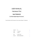
GUITAR EFFECT PEDALS IMPLEMENTATION IN ALTERA DE2 BOARD
NIK MOHD FARHAN SHAH BIN ABD RAZAK
A report submitted in partial fulfillment of the
requirements for the award of the degree of
Bachelor of Engineering (Electric-Microelectronics)
Faculty of Electrical
Universiti Teknologi Malaysia
MAY 2011
ii
I declare that this report entitled “Guitar Effect Pedals Implementation in Altera DE2
Board” is the result of my own research except as cited in the references. The report
has not been accepted for any degree and is not concurrently submitted in
candidature of any other degree.
Signature
: .......................................
Name
: NIK MOHD FARHAN SHAH BIN ABD RAZAK
Date
: 20 MAY 2011
iii
Special dedicated to my beloved parents, ma and abah, beloved siblings,
to all my beloved friends,
and to others who encouraged me throughout my journey of education
A warm thanks to all.
iv
ACKNOWLEDGEMENT
In the Name of ALLAH, the Most Beneficent, the Most Merciful.
My utmost thanks and gratitude goes to my family for their loving and
continuous support throughout the years of my life. Thanks for their encouragement,
love and emotional supports that they had given to me. Without them, I will never be
able to make it this far.
I would like to express my deepest appreciation to my project supervisor, Dr.
Shaikh Nasir Shaikh Hussin for his guidance and valuable advices which have helped
me a lot in completing my project. My appreciation also goes to the staffs of ECAD Lab
of FKE who have provided me the facilities and co-operations to carry out my project.
Special thanks dedicated to my friends especially the SEW students who have
been supporting, guiding and advising me toward completion of this project and also
this thesis. Thanks to all my friends for all the care and concerns, that has supported me
throughout my journey in UTM.
Last but not least, appreciation is extended to those who have contributed
directly or indirectly during completion of this project.
v
ABSTRACT
This project reports the implementation of digital guitar effect processors on
Altera DE2 development board. This project deals with analog signal processing where
signals are sent to DE2 board when the guitar player play the guitar that is connected
through line in port. In order to perform the digital signal processing, the analog audio
signal is first converted to digitized audio data by using the WM8731 audio CODEC
chip in DE2 board. This audio CODEC chip must be configured correctly. Guitar effect
processors are implemented into FPGA to perform the digital processing for those
digitized audio data. These guitar effect processors will be contain of two types of
effects which is the distortion effect and delay/echo effect where they are developed and
implemented in the FPGA architecture with VHDL language. The processed audio data
is then converted back to analog signal and sent to the speaker for the sound
amplification through line out port.
vi
ABSTRAK
Projek ini melaporkan pemuatan efek gitar prosesor digital pada papan
pembangunan Altera DE2. Projek ini akan berurusan dengan pemprosesan isyarat
analog di mana isyarat ini akan dihantar ke papan DE2 pada ketika pemain gitar sedang
bermain gitar yang disambungkan kepada saluran line in jack. Dalam rangka untuk
melakukan pemprosesan isyarat digital, isyarat audio analog hendaklah terlebih dahulu
ditukar menjadi data audio digital dengan menggunakan cip audio CODEC WM8731
dalam board DE2. Cip audio CODEC ini haruslah diaturcarakan supaya sesuai untuk
membuatnya berpadanan bekerja dengan projek. Prosesor efek gitar diimplementasikan
ke dalam FPGA untuk melakukan pemprosesan digital untuk data audio yang telah
didigitalkan. Prosesor efek gitar akan mengandungi dua jenis kesan yang merupakan
kesan distorsi dan menunda / kesan gema yang mana ianya akan dibangunkan dan
dilaksanakan dalam seni bina FPGA dengan bahasa VHDL. Data audio yang diproses
kemudian ditukar kembali ke isyarat analog dan dihantar ke speaker untuk amplifikasi
bunyi melalui line out jack.
vii
TABLE OF CONTENTS
CHAPTER
1
2
TITLE
PAGE
FRONT PAGE
i
DECLARATION
ii
DEDICATION
iii
ACKKNOWLEDGEMENT
iv
ABSTRACT
v
ABSTRAK
vi
TABLE OF CONTENTS
vii
LIST OF TABLE
x
LIST OF FIGURES
xi
LIST OF ABBREVIATIONS
xiii
LIST OF APPENDICES
xiv
INTRODUCTION
1
1.1
Introduction to Altera DE2 board
2
1.2
Introduction of DSP with FPGA
5
1.3
Introduction of Guitar Effect Pedals
7
1.4
Problem Statement
8
1.5
Objectives
9
1.6
Scopes of Study
9
1.7
Methodology
11
LITERATURE REVIEW
12
2.1
Signal Processing for the Electric Guitar
12
2.2
Electric Guitar Distortion Pedal Design
13
2.3
Electric Guitar Delay Pedal Design
14
2.4
Principle DSP of Analog Signal
15
viii
3
4
AUDIO CODEC WM8731 CONTROL
17
3.1
I2C Bus Controller
17
3.2
WM8731 Register Map
19
GUITAR EFFECT PROCESSOR MODELLING
24
4.1
System Overview
24
4.2
Audio Deserializer
26
4.3
Audio Serializer
28
4.4
Guitar Effect Processors
30
4.5
Distortion Effect Processor
31
4.5.1
Core design for Distortion Effect Processor
32
4.5.2
Distortion Effect Processor in Full Spec
4.6
Design
33
Delay Effect Processor
34
4.6.1
Core Design for Delay Effect Processor
36
4.6.1
Delay Effect Processor in Full Spec
Design
4.7
5
Design Implementation into DE2 board
36
37
RESULT AND DISCUSSIONS
39
5.1
Design Simulation for Audio Deserializer
39
5.2
Design Simulation for Audio Serializer
40
5.3
Design Simulation for Distortion Effect Module
41
5.4
Design Simulation for Delay Effect Module
42
5.5
Guitar Effect Processor Design in Real View
42
5.5
Bypass Sound from Guitar Effect
Processor Hardware
5.6
43
Sounds from Distortion Effect
Processor Hardware
44
5.7
Sounds from Delay Effect Processor Hardware
45
5.8
Sounds from Both of the Effects is Activated
45
ix
6
CONCLUSSION AND RECOMMENDATION
47
6.1
Conclusion
47
6.2
Problem Highlights
48
5.3
Recommendations for Future Works
48
REFERENCES
APPENDIXES
50
A-B
x
LIST OF TABLES
TABLE NO.
TITLE
PAGE
1.1
DE2 board information
3
3.1
2-Wire MPU Interface Address Selection
18
3.2
Register map for WM8731
20
3.3
Register map address for each corresponding settings
20
3.4
Analog audio path control
21
3.5
WM8731 pin assignment in FPGA
23
xi
LIST OF FIGURES
FIGURE NO.
TITLE
PAGE
1.1
Altera DE2 development and education board
2
1.2
Block diagram of the DE2 board
4
1.3
Schematic diagram for chip WM8731
6
1.4
Metal-zone guitar effect pedal
7
1.5
Overall progress for this project
10
1.6
Design synthesis guidelines
11
2.1
Basic configuration of guitar’s signal processing
13
2.2
Example of a distorted waveform
14
2.3
Delay/Echo effect system flow
15
2.4
Scheme for the digital processing of an analog signal
16
3.1
Data transmission through I2C using 2-wire serial
interface mode
18
3.2
Settings used for WM8731 register map
22
3.3
Digital Audio Interface in master mode
23
4.1
Block diagram for the guitar effect sound system
24
4.2
System overview
25
4.3
Data transmission in Left Justified mode
26
4.4
Audio Deserializer state diagram design
27
4.5
Audio Deserializer module design
28
4.6
Audio Serializer state diagram design
29
4.7
Audio Serializer module design
29
4.8
Guitar Effect Processor System
30
4.9
Block diagram of Distortion Effect Module
31
4.10
Core design for Distortion Effect Processor
33
4.11
Distortion Effect Processor
34
4.12
Delay effect design
34
xii
4.13
Delay Effect Module buffer design architecture
35
4.14
Core design for Delay Effect Processor
36
4.15
Delay Effect Processor
37
4.16
Guitar Effect Processor Block Diagram
38
5.1
Design Simulation for Audio Deserializer module
40
5.2
Design Simulation for Audio Serializer module
40
5.3
Simulation for Distortion Effect Module
41
5.4
Simulation for Delay Effect Module
42
5.5
Actual view of Guitar Effect Processor System
43
xiii
LIST OF ABBREVIATIONS
DSP
-
Digital Signal Processing
FPGA
-
Field Programmable Logic Array
PDSP
-
Programmable Digital Signal Processor
ADC
-
Analog Digital Converter
DAC
-
Digital Analog Converter
I2C
-
Inter Integrated Circuit
HDL
-
Hardware Design Language
VHSICHDL -
Very High Speed Integrated Circuit Hardware Design
Language
CAD
-
Computer aid design
RAM
-
Random Access Memory
xiv
LIST OF APPENDICES
APPENDIX
TITLE
PAGE
A
VERILOG CODE OF WM8731 CONTROL
52
B
VHDL CODE OF GUITAR EFFECT PROCESSOR
60
CHAPTER 1
INTRODUCTION
Music is an important part of most people‟s lives where it can entertain and
bring joy to those who are listening to it. Listening to music changes our emotions [1, 2,
3], our moods [4], our efficiency [5], our shopping behavior [6] and even our eating
behavior [7, 8]. Music can come from many sources and guitar is one of the good
instruments that can be played to produce a nice sound to compose the music. Since the
invention of the electric guitar within the year of 1940, many guitar effects has been
purposely created in order to change and to make the sound of the guitar become more
interesting and can be adapted to certain style of music. Since then, most of the invented
guitar effects are designed in the form of analog circuitry. Nowadays, the audio signal
processing has become more and more developed especially in the field of Digital
Signal Processing (DSP). Meanwhile, at the present time, Electronic Industry has
offered us new possibilities to develop our own digital hardware without spending such
high quantities of money. For example, the use of Field Programmable Gate Array
(FPGA) can essentially allows the developer to develop as many designs as they wanted
to by using only a single chip of the FPGA in which, it can be reprogrammed as if it
were a software-based system. FPGA are on the verge of revolutionizing digital signal
processing in the manner that programmable digital signal processor (PDSP) did nearly
two decades ago [9].The upcoming technology of complete systems on a single
programmable chip contrasts such a software centric solution, because it combines
2
software and hardware via some co-design methodology and makes for a promising
alternative for the future of real-time audio.
1.1
Introduction to Altera DE2 board
The Altera Development and Education (DE2) board from Terasic Technologies
Inc. is a wonderful platform for learning about digital logic, computer organization, and
FPGAs. Featuring an Altera Cyclone II FPGA, the DE2 board offers varied technology
suitable for university and college laboratory use, a wide range of design projects, as
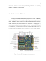
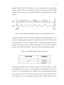
well as sophisticated digital system development tools [10]. A picture of the DE2 board
is shown in Figure 1.1. It depicts the layout of the board and indicates the location of
the connectors and key components which is available to be used for multiple purposes.
Figure 1.1: Altera DE2 development and education board
3
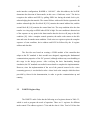
The following hardware is provided on the DE2 board:
Table 1.1: DE2 board information
Feature
Description
FPGA
• Cyclone II EP2C35F672C6 with EPCS16 16-Mbit serial configuration device
Devices
• Built-in USB-Blaster cable for FPGA configuration
• 10/100 Ethernet
• RS232
• Video Out (VGA 10-bit DAC)
• Video In (NTSC/PAL/Multi-format)
• USB 2.0 (type A and type B)
• PS/2 mouse or keyboard port
• Line In/Out, Microphone In (24-bit Audio CODEC)
• Expansion headers (76 signal pins)
• Infrared port
Memory • 8-MBytes SDRAM, 512K SRAM, 4-MBytes Flash
• SD memory card slot
Display
• 16 x 2 LCD display
• Eight 7-segment displays
Switches • 18 toggle switches
and
• 18 red LEDs
LEDs
• 9 green LEDs
• Four debounced pushbutton switches
Clocks
• 50 MHz crystal for FPGA clock input
• 27 MHz crystal for video applications
• External SMA clock input
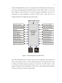
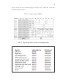
In addition to these hardware features, the DE2 board has software support for standard
I/O interfaces and a control panel facility for accessing various components. The
computer aid design (CAD) tool represent as the software of Quartus II Web Edition
4
and Nios II Embedded Processor is a compliment for the DE2 board that allows the user
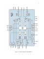
to develop any design and then implement them into the FPGA. Figure 1.2 gives the
block diagram of the DE2 board. To provide maximum flexibility for the user, all
connections are made through the Cyclone II FPGA device. Thus, the user can
configure the FPGA to implement any system design.
Figure 1.2: Block diagram of the DE2 board
All of this enhancement can be used to allow the user to implement various designs of
circuits, from simple circuits to various multimedia projects in which can also be used
to dealing with digital signal processing for sound since this DE2 board is fully
equipped with audio codec chip hardware which can be used to digitized the sound data
to be processed into our own processing design
5
1.2
Introduction of DSP with FPGA
DSP techniques have been used in wide variety of areas including audio
processing, image processing, and control, instrumentation and communication system.
The application for DSP included digital filter, image compression, speech recognition,
and digital audio. FPGAs offer a more native implementation for most DSP algorithms.
Each task is allocated its own resources, and runs independently. It intuitively makes
more sense to process each step of a continuously streaming signal processing chain in
an assembly line-like process, with dedicated resources for each step [11]. This yields
compact, low power, and low cost digital design.
Audio processing is one of the digital signals processing with analog input. So,
in audio system, the analog audio signal is first converted to digitized audio data and
after that only the signal can be processed within user-define system. For this purpose,
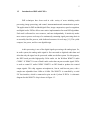
the DE2 board provides high-quality 24-bit audio via the Wolfson WM8731 audio
CODEC. IC WM8731 is one of kind‟s audio codec that can process audio signal. FPGA
is used to control IC audio CODEC WM8731 on DE2 board to produce the wanted
output signals. This chip supports microphone-in, line-in, and line-out ports, with a
sample rate adjustable from 8 kHz to 96 kHz. The WM8731 is controlled by a serial
I2C bus interface, which is connected to pins on the Cyclone II FPGA. A schematic
diagram for this WM8731 chip is shown in Figure 1.3.
6
Figure 1.3: Schematic diagram for chip WM8731
7
1.3
Introduction of Guitar Effect Pedals
In many guitar player‟s careers, there comes a time when they are unable to find
an appropriate sound with their guitar and amp, no matter how much tweaking and finetuning is done. In these situations, guitarists will often use effects pedals to alter their
instrument's sound in a particular manner. There are many, many different types of
effects that can be found for the guitar. For example, there is reverb, fuzz, delay, chorus,
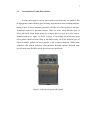
distortion and so on. Figure 1.4 shows a picture of an example for metal-zone guitar
effect pedals which has been selling in the market today. Of all the different types of
effects available, perhaps the most popular is still overdrive/distortion. While many
amplifiers offer built-in distortion, often guitarists find that separate distortion units
provide more tonal flexibility and to give them more satisfaction.
Figure 1.4: Metal-zone guitar effect pedal
8
1.4
Problem Statement
Design exploration based on the DE2 board enhancement had not yet fully being
used by UTM‟s undergraduate student. The component of ADC and DAC part within
the DE2 board has never been used by any of our undergraduate student. This is a good
opportunity to explore this features of the DE2 board in the purpose to modeling our
own guitar effects and it is indeed will be a worthy effort since it can be used for the
future students of UTM to do other project that need to be dealing with ADC and DAC
such as the project of voice recognition
Meanwhile, a single guitar effect pedal price in the market is mostly rated at the
price more than $100 USD [12] and the price of the DE2 board is normally sold at $495
USD, but for academic purpose, it is sold at the price of $269 USD [13]. If we are to
compare the price of a single DE2 board with a single guitar effect pedals, it is indeed
that the price of the DE2 board are much higher. However, despite that fact, by using
DE2 board, we can actually modeling multiple of our own guitar effects while applying
knowledge within various scopes in order to implement the effects into only a FPGA of
the DE2 board. Just imagine, if we can implement 3 of the guitar effect into a single
DE2 board, then the price of the DE2 board won‟t be a matter as if it is in a need to
argue.
Besides that, it is much easier to modeling the guitar effect model by using the
method of Hardware/Software co-design approach for embedded system design since by
this way; we do not have to spend high quantities of money and time. Any design can be
synthesis to verify its output by using the CAD tools of Quartus II and this is a very
convenient way to debug and fix the problem within the design rather than to modeling
the guitar effect as in the form of analog hardware.
9
1.5
Objectives
The main objective of this project is to produce a Guitar Effect Processor sound
system by implementing some of the guitar effects pedals design into DE2 board which
are:
i.
Distortion Effect Processor: this model will boost and clips the guitar
signal at specific maximum and minimum value and this will produce an
overdriven guitar sound.
ii.
Delay/Chorus Effect Processor: this model will make guitar sound like
multiple guitars.
1.6
Scopes of Study
This scope of the project is mainly focused on the studying and understanding
the Altera DE2 development board. Since the usage of ADC and DAC component
within this platform is not yet being used by our students, further exploration based on
that particular part is indeed a good opportunity. Generally, this is the scopes that we
will be dealing with in order to complete this project:
i.
Application of DSP knowledge to create the guitar effects.
ii.
Application of the programming skills in Hardware Design Language
(HDL) to realize the effects design.
iii.
Application of computer skills to generate the effects based on the
specified software.
iv.
Application of the Hardware/Software co-design approach for embedded
system design.
10
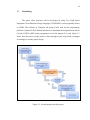
1.7
Methodology
The guitar effect processor will be developed by using Very High Speed
Integrated Circuit Hardware Design Language (VHSICHDL) or more popularly known
as VHDL. The software of Computer aid design (CAD) used for the programming
platform is Quartus II Web Edition and then as to download the design them the Altera
Cyclone II FPGA (DE2 board), programmer tool in the Quartus II is used. Figure 1.5
shows how the process of this project is done through several step which is arranged
accordingly to ease the project design.
Figure 1.5: Overall progress for this project
11
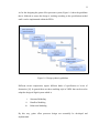
As for the designing the guitar effect processor system, Figure 1.6 show the guidelines
that is followed to ensure the design is working according to the specification needed
until it can be implemented within the FPGA.
Figure 1.6: Design synthesis guidelines
Different circuit complexities require different kinds of specification or levels of
abstraction [14]. In general there are three modeling style in VHDL that can be used to
adapt the design of digital system which is:
i.
Structural Modeling
ii.
Dataflow Modeling
iii.
Behavioral Modeling
By this way, guitar effect processor design can essentially be developed and
implemented.
12
CHAPTER 2
LITERATURE REVIEW
This chapter will discuss briefly about the theory and research from other
researchers related to the project.
2.1
Signal Processing for the Electric Guitar
An acoustic guitars sound is largely dependent on the vibration of the guitar's
body and the air within it; the sound of an electric guitar is largely dependent on an
electrical signal, generated by the vibration of the strings and shaped on its path to the
amplifier. By the late 1960s, it became common practice to exploit this dependence to
alter the sound of the instrument. The most dramatic innovation was the generation of
distortion by increasing the gain, or volume, of the preamplifier in order to clip the
electronic signal. This form of distortion generates harmonics, particularly in odd
multiples of the input frequency, which are considered pleasing to the ear. Basically,
Figure 2.1 shows how does the signal from the guitar is processed where this signal
flows through from guitar through cable to a series of signal processing circuitry which
can be any guitar effect pedals, and then is sent through the speakers of a guitar
amplifier. By the 1980s and 1990s, digital effects became capable of replicating the
13
analog effects used in the past. These new digital effects attempted to model the sound
produced by analog effects, to varying degrees of quality. Hence the use of the FPGA to
modeling digital guitar effects would create a new possibility of phenomena in the new
design of guitar effects.
Figure 2.1: Basic configuration of guitar‟s signal processing
2.2
Electric Guitar Distortion Pedal Design
Distortion of a guitar signal is created by clipping. There are two basic types of
distortion for guitar: soft clipping and hard clipping. Soft clipping is generally referred
to by members of the music industry as “overdrive”, while hard clipping is commonly
called “distortion”. This pedal is a heavy metal distortion effect, and heavy metal guitar
sound is created by almost exclusively hard clipping circuitry for the crucial heavily
distorted sound that is defines the genre of music. From this point on, the term
“distortion” will be used to refer to hard clipping, which in the most basic sense is
clipping the peaks and troughs off of the sinusoidal signal that makes up any audio
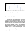
signal. Figure 1.8 is an example of a distorted waveform.
14
Figure 2.2: Example of a distorted waveform
2.3
Electric Guitar Delay Pedal Design
In popular and electronic music, electric guitarists use delay to produce densely
overlaid textures of notes with rhythms complementary to the music. Vocalists and other
instrumentalists use it to add a dense or ethereal quality to their playing. Extremely long
delays of 10 seconds or more are often used to create loops of a whole musical phrase.
These effects can reproduce whole chunks of the original sound at particular time-based
intervals, so the detail of the part can be mostly preserved. A delay circuit memorizes
the audio signal and plays it back after a delay time from several milliseconds to several
seconds. Most delays will have a feedback control (or regeneration) which takes the
output of the delay, and sends it back to the input. If the feedback gain is less than one,
the sound will repeat over and over, becoming quieter each time it plays back. In short, a
simple circuit delay takes an audio signal, and plays it back after the delay time. The
delay time can range from several milliseconds to several seconds.
15
Figure 2.3: Delay/Echo effect system flow
2.4
Principle DSP of Analog Signal
Since this project will be dealing with analog input signal which comes from the
guitar, therefore a little briefing in DSP of analog signal would be a good approach.
Digital signal processing is distinguished from other areas in computer science by the
unique type of data it uses, which are signals. In most cases, these signals originate as
sensory data from the real world: seismic vibrations, visual images, and sound waves
[15]. DSP is the mathematics, the algorithms, and the techniques used to manipulate
these signals after they have been converted into a digital form. This includes a wide
variety of goals, such as enhancement of visual images, recognition and generation of
speech, and compression of data for storage and transmission. Digital signal processing
of an analog signal can divided into three basic steps.
i.
Conversion of the analog signal into digital data
ii.
Processing of the digital data
iii.
Lastly, reconversion of the processed digital data into analog signal
16
These three basic steps can be show in block diagram Figure 2.3.
Figure 2.4: Scheme for the digital processing of an analog signal
Since the amplitude of analog input signal varies with time. Thus, a sample and
hold circuit is needed before the analog digital conversion (ADC). The sample and hold
circuit samples the analog signal at uniform interval and holds the sampled value
constant after each sampling operation for sufficient time for accurate digital conversion
by ADC. By this way, we can ensure the input signal from the analog input will not
damage the component of ADC. The input to the ADC converter is a staircase-type
analog signal if the Sample and Hold circuit holds the value until the next sampling
instant [16]. The output of ADC is a binary data stream or a sequence of word. Each
word represents a sample of the sequence. The word length of ADC output is given
number of bit, limits the achievable dynamic range of the converter and accuracy to
representing input analog signal [16]. The digital signal is then processed by the digital
processor or FPGA where various design can be implemented to process the data. The
output of the digital processor is converted into analog signal by digital analog converter
(DAC).
17
CHAPTER 3
AUDIO CODEC WM8731 CONTROL
Among all, this is the critical things that need to be concerned. We must first set
a right configuration of mode or criteria for WM8731 to operate with. If the codec chip
is not configured accordingly then we might just end up getting no sound produced or
might as well keep producing a clean sound that comes from guitar without being
processed at all due to the bypass looping operation. In Figure 1.3 of Section 1.2, the
codec chip can be configured through Control Interface by using either using either 3wire serial interface or 2-wire serial interface [17], meanwhile the data and alignment
clock to be processed can be obtained from Digital Audio Interface.
3.1
I2C Bus Controller
The FPGA communicates with the WM8731 via the I2C (Inter-Integrated
Circuit) protocol using two pins: 'SDIN' (the data line), and 'SCLK' (the bus clock)
Figure 3.1 shows the complete requirement of data transmission through I2C by using 2
wire mode control protocol that is used for this project. Within the procedure of the I2C
bus, unique situations arise which are defined as START and STOP conditions. START
means a high to low transition on the SDIN line while SCLK is high and STOP means a
low to high transition on the SDIN line while SCLK is high .The master always
18
generates START and STOP conditions. The bus is considered to be busy after the
START condition. The bus is considered to be free again a certain time after the STOP
condition. The bus stays busy if a repeated START is generated instead of a STOP
condition.
Figure 3.1: Data transmission through I2C using 2-wire serial interface mode
The data input signal is SDIN. It contains the information for the control interface. The
controller was reprogrammed using the 2-wire interface with the EP2C35F672C6 FPGA
in Cyclone II board. After the start condition that is a falling edge on SDIN while SCLK
is high. The following seven bits determines which device receives the data which in
this case is the CODEC chip. Table 3.1 shows the 2-Wire Interface address selection.
Table 3.1: 2-Wire MPU Interface Address Selection
The transfer is MSB first. The 7-bit address consists of a 6-bit base address + a single
programmable bit to select one of two available addresses for this device. The first 6 bit
of “001101” is the fixed address for the CODEC chip. The remaining address depends
on the CSB state where for 2-wire mode interface, the state of the MODE pin of the
most LSB bit is set as „0‟. Consequently, the address for the CODEC chip with 2-wire
19
mode interface configuration, RADDR is “0011010”. After this address, the bit R/W
determines the direction of data transfer, in this case a „0‟indicates „write‟. The device
recognizes the address and R/W by pulling SDIN low during the ninth clock cycle,
acknowledging the data transfer. The control follows with two bit blocks (separated with
another acknowledge) the first block B [15:9] contains the control address bits, and the
second block B [8-0] contains the control data bits. The stop condition after the data
transfer is a rising edge on SDIN when SCLK is high. If a start condition is detected out
of the sequence at any point in the data transfer then the device will jump to the idle
condition [18]. After a complete control operation, the audio codec returns to the idle
state and waits for another start condition. Each write to a register requires the complete
sequence of start condition, device address and R/W bit followed by the 16 register
address and data bits.
The first idea was based on creating a VHDL module of the controller that
adapts to the I2C standard. A basic module was designed, supporting the fundamental
communication properties of the I2C protocol, although without any error handling at
this stage in the design process. After verifying the basic functionality through
simulation, the I2C standard was studied in more detail to complete the implementation.
However, since the implementation of the rest of the protocol seemed to be a time
consuming process, it was decided to take a closer look at the example which has been
provided by Altera for the demonstration, in order to get the communication up and
running
3.2
WM8731 Register Map
The WM8731 audio Codec has the following set of registers shown in Table 3.2,
which is used to program the mode of operation. There are 11 registers for different
mode control. The address register is 7 bits and the data is 9 bits. Total of 16 bits data
20
will be inserted in series to SDIN input port on audio codec with SCLK as what has
been discussed in Section 3.1
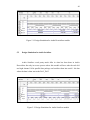
Table 3.2: Register map for WM8731
Table 3.3: Register map address for each corresponding settings
21
As we can see from the simplified register map in Table 3.2, the „X‟ notation is
the data to be computed by the user. For example, to set the analog audio path control,
register of address 0000100 is used. Then, by referring to the table provided in the
datasheet, Table 3.3, data for each bit is carefully chosen. Since the audio data need to
be processed, set to disable the bypass which now bit 3 is „0‟.Reset bit 2 to chose line-in
as the input port for the guitar. Enable mute for microphone input (bit 1 is ‟1‟), disable
boost (bit 0 is „0‟) and as well as the sidetone (bit 5 is „0‟) because we are not using this
input port. Mind as well to select DAC (bit 4 is „1‟) since the processed data will be sent
to output immediately after processing, thus DAC is always in ON condition.
Table 3.4: Analog audio path control
Bit selection for side tone selection is taking up the default value which now bit 7:6 is
„00‟. For all specification above, the data register of Analog Audio Path Control is
000010010. Thus, the value "0000100000010010" is sent to SDIN to set the
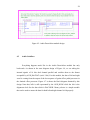
configuration of analog audio path. Others register can be set using the same method.
The setting used for the purpose of this project can be found in Figure 3.2.
22
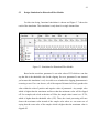
Figure 3.2: Settings used for WM8731 register map
WM8731 may be operated in either one of the 4 offered audio interface modes.
All four of these modes are MSB first and operate with data 16 to 32 bits. These are:
right justified, left justified, I2S, and DSP mode and this can be set in Digital Audio
Interface Format register. For this project, 16 bit audio data length is selected with left
justified format and with 48 KHz sampling rate. Carefully set the base over sampling
rate (BOSR) in Sampling Control register because it is important to have the exact
sampling rate based on the master clock for the device (refer to datasheet[17] : Table 19
& 20 ,page 40).
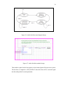
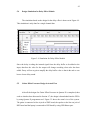
The codec was set to operate in master mode in which the audio-codec provides
all signals for synchronization of audio data with the FPGA in this system, including
BCLK, ADCLRCK and DACLRCK as shown in Figure 3.3. Meanwhile in slave mode,
the codec depends on both master clock, BCLK, ADCLRCK and DACLRCK from an
external module, in this case the FPGA. All of these settings play a big role when we are
going to receive the data from Digital Audio Interface to be processed. When all of
these have been configured, carefully do the pin assignment in the FPGA for each input
and output regarding with WM8371 codec chip by referring to the Table 3.4.
23
Figure 3.3: Digital Audio Interface in master mode
Table 3.5: WM8731 pin assignment in FPGA
24
CHAPTER 4
GUITAR EFFECT PROCESSOR MODELLING
In order to design the guitar effect processor, a complete sound system for the
guitar effect processor must first be developed so that all of the bussing and interface
can be done easily later until the integration and implementation in the FPGA. Then
after that, a single unit for each component design can be developed.
4.1
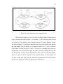
System Overview
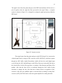
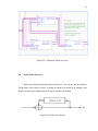
This system will be equipped by using a guitar, a DE2 board, and a pair of
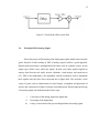
speakers. Basically, the block diagram for this effect sound system is shown as below.
Figure 4.1: Block diagram for the guitar effect sound system
25
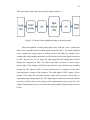
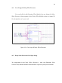
The signal comes from the guitar and goes to the DE2 board and then will be sent to a
pair of speakers after the signal has been processed in the signal. Hence, a complete
system as shown in Figure 4.2 is designed to routing the signal processing within the
DE2 board.
Figure 4.2: System overview
The signal comes from the guitar and goes to the FPGA board. It is converted to
a digital signal first by using an ADC converter (AUD_ADCDAT), and then it passes
through an ADC buffer (Audio Deserializer) which will take the serial digital input
received from the ADC and buffering it so the Effects Processor can modify the data to
the desired effect. In this effect processor, it contains of the distortion and delay effect
module. After that the data will be re-serialized through the DAC buffer (Audio
Serializer) to change the bit of the data into a format which is acceptable to DAC
converter. After this, the modified signal is converted back to analog by using DAC
converter (AUD_DACDAT) and is sent to the guitar amplifier for sound generation.
26
The interface with the development board was the switches to select the effect and the
LCD will be used to show which effect has been chosen. Meanwhile, to control the
volume strength, the buttons on the DE2 board will be used.
4.2
Audio Deserializer
Since the input that comes from AUD_ADCDAT (ADC converter) is serial 1
bit, thus we have to make some necessary processing to accumulate the data into 16 bit
and feed them to each left and right channel. From Section 3.2, the format chosen for the
data is left justified. From Figure 4.3, Left Justified mode is where the MSB is available
on the first rising edge of BCLK following a ADCLRCK or DACLRCK transition with
the left channel data are present when the alignment clock for ADC/DAC is „1‟ and vice
versa for the right channel data. While in Figure 4.4, it shows the state diagram for
Audio Deserializer module design in the project.
Figure 4.3: Data transmission in Left Justified mode
27
Figure 4.4: Audio Deserializer state diagram design
The audio data width is set to be 16-bit in the Digital Audio Format Interface
such as what has been show in Figure 3.2 of Section 3.2. The received adc data is stored
in a register of 32 bit width by using a counter looping of 32 count. When the counter
has finish counting to 32, then the accumulated data is sent to left channel first and then
the right channel. The left channel will be taking the data bit of 31 until 16 while the
right channel is taking the bit of 15 until 0. This process is repeated again when new
data package is received and once again, the counter will start counting and wait until
the data package is fully received and transfer it again to the left and right channel.
Figure 4.5 shows the block diagram for this particular design. For this module, the
adc_data is taken from ADC_DAT pin, while bclk represent as the AUD_BCLK while
the lrck is the alignment clock for adc data which is ADCLRCK.
28
Figure 4.5: Audio Deserializer module design
4.3
Audio Serializer
Everything happens much like in the Audio Deserializer module but only
backwards. As shown in the state diagram design of Figure 4.6, we are taking the
internal signals of 16 bits dual channel parallel and serialize them to the format
acceptable by AUD_DACDAT (serial 1 bit). For this module, the data of left and right
word is coming from the output of the last sequence of guitar effect pedal processor in
the chained effect processor. Figure 4.7 is shows the block diagram obtained by this
design. Note that, bclk is still represented by the AUD_BCLK while the lrck is the
alignment clock for dac data which is DACLRCK. Mono_selector is a simple module
that can be used to ensure the data for both left and right channel is fed properly.
29
Figure 4.6: Audio Serializer state diagram design
Figure 4.7: Audio Serializer module design
This module is placed at the last sequence in the chained guitar effect processor system.
The dac data is assigned to AUD_DACDAT where this data will be converted again
into the analog form for sound generation.
30
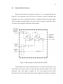
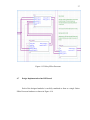
4.4
Guitar Effect Processors
This is the part where we will develop and design the digital effect processor
which is the Distortion Effect Processor and Delay Effect Processor, and then integrates
them into a higher structural design in the Guitar Effect Processor. Figure 4.8 shows a
view on how the effect processor is designed and arranged. It was arranged in a chain
sequence so that the user can play two effects at the same time. A 16-bit sample input
which comes from the Audio Deserializer supply inputs for the Distortion Processor.
Bypass module is included in each effect processor where the original sound of the
guitar will be let through without any change or modification is done to it. The user will
dictate which effect module to use by using the switch on the DE2 board and supply a
gain and phase input parameter to control the strength of the effect by using buttons key
on the DE2 board. The processed data is next sent to Audio Serializer module to change
the bit of the data into the acceptable format by DACDAT.
Figure 4.8: Guitar Effect Processor System
31
4.5
Distortion Effect Processor
Based on what has been discussed in section 2.2, we can understand that the
behavior of the distortion circuit will clip the waveform at specific maximum and
minimum value. Thus, to design this module, a comparison between the input sample
and the parameter controlled by the user can be used to control the output data. Figure
4.9 shows a block diagram of Distortion Effect Module.
Figure 4.9: Block diagram of Distortion Effect Module
In this module, this is where a threshold value is set which is the parameter1, and
if the signal ever increases above this value and lower than the negative value of this
parameter1 value, then signal is clipped off. The 16-bit output fed from Audio
Deserializer will be fed as the sample into the first comparator. Meanwhile, 16-bit input
32
of parameter 2 will be send to both of the two comparators in the module. The first
comparator will output a „1‟ if the sample is greater than parameter1 and the signal is
then sent to the first mux. When „1‟ is sent into the first mux, it will choose the
parameter2 as the output of the mux and if „0‟ is inserted into the mux, it will allow the
value of the sample to pass through. After that, the same process is repeated again, but
this time, it will only allow the sample value to pass through as the output of the second
mux if it is smaller enough than the negative value of parameter1. By this way, there
will be no value that can be higher than positive value of parameter1 and lower than
negative value of parameter1. Thus a clipped output signal is produced which is then
amplified by parameter2 to make the sound becomes clearer when it is played on the
speakers later.
4.5.1
Core Design for Distortion Effect Processor
The core design for Distortion Effect Processor is the integration of two
Distortion Effect Module so that two channel of left and right data can be processed. As
shown in Figure 4.10, volume module is some sort of the design for parameter2 as we
can see in Figure 4.9 but instead it was designed as a single part so that we can use it for
various purposes in another design later on. It functions as volume gain and is added at
the output of the distortion block so that we can hear a clearer sound. The threshold
parameter is in the thresh_param where the user can easily select the threshold
parameter by using the switch assigned in the higher hierarchal structure.
33
Figure 4.10: Core design for Distortion Effect Processor
4.5.2
Distortion Effect Processor in Full Spec Design
The Distortion Effect module is now being arranged to fit into the Distortion
Effect Processor such as in Figure 4.11, where it contains along with Bypass module
and Pipeline Buffer module. Bypass module will operate as the selector to turn on or off
the effect meanwhile Pipeline Buffer module is assigned as a stabilizer in which it will
rearrange the output that comes from Bypass module into the right 16 bit data package.
It is introduced after each effect to take care of timing violations. All these buffers are
however clocked with the 50 MHz system clock whereas the sound is sampled at 48
kHz. This means that roughly 1000 of those would need to be introduced into the system
to cause a system latency of over one sample [19].
34
Figure 4.11: Distortion Effect Processor
4.6
Delay Effect Processor
Based on what have been discussed in Section 2.3, we can see that the behavior
for the delay effect circuit is that it is taking the input to be stored in the memory and
then the stored data is added again to the input to produce the output.
Figure 4.12: Delay effect design
35
The delay effect buffers a fragment of the audio signal in memory and mixes it back into
the output signal. The effect's output is fed back into the delay unit, creating a decaying,
infinite response. There is several ways on how we could have store the data of the
input. Usually, RAM is used as a storage component, however for this particular design,
array have been choose as a storage to temporarily store the input data which then will
be shifted until 10 times. The internal shifted data can be taken as a loop to be added to
input again. Figure 4.8 is the general delay buffer design architecture. To produce
different sound of delay, we can take different value of the internal delay buffer to be
added into input again. Suppose the higher value of the internal value is taken, for
example the value in Reg 5, the sound will have longer delay time rather than Reg 2. For
the following Delay Effect Module, For the first type which when delay_type is at „0‟,
the value of Reg 0 is taken to be added with the input meanwhile when delay_type is
triggered to „1‟, value of Reg 5 is taken as a summation to the input. Decay will act as
amplifier to control the volume of the feedback sound.
Figure 4.13: Delay Effect Module buffer design architecture
36
4.6.1
Core Design for Delay Effect Processor
Very much alike in the Distortion Effect Module, the core design for Delay
Effect Processor is the integration of two Delay Effect Module so that two channel of
left and right data can be processed.
Figure 4.14: Core design for Delay Effect Processor
4.6.2
Delay Effect Processor in Full Spec Design
The arrangement for the Delay Effect Processor is same with Distortion Effect
Processor. Only that the Distortion Effect Module is replaced by Delay Effect Module.
37
Figure 4.15: Delay Effect Processor
4.7
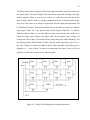
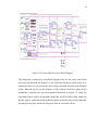
Design Implementation into DE2 board
Each of the designed modules is carefully combined to form as a single Guitar
Effect Processor hardware as shown in Figure 4.16.
38
Figure 4.16: Guitar Effect Processor Block Diagram
This integration is achieved by using block diagram where we can easily made all the
bus connection between the modules. It also makes the hardware system easier to be
understood where we can see how the data is being controlled and processed within the
system. When the top level of the hardware is fully combined, then once again, the pin
assignment is ensured to be correctly mapped as mentioned in Section 3.2. Lastly, the
programmer tool is used to download the design into the FPGA (DE2 board). Make sure
that the guitar is connected to line in and the speaker to the line out port. Else than that,
just start play the guitar and use the assigned switch to activate the effects.
39
CHAPTER 5
RESULT AND DISCUSSIONS
The chapter will discuss about the result achieved from the Guitar Effect
Processor which has been implemented into the FPGA of Cyclone II EP2C35F672C6 in
the DE2 board platform. Along with this, some briefing about the simulation result
obtain from Quartus II for crucial part in the project is also included
5.1
Design Simulation for Audio Deserializer
The design for both of Audio Deserializer is considered as very important in this
project. This is because this particular part will determine the right data is sent to be
processed in the effect processor by receiving the data from ADC_DAT. The design
simulation for Audio Deserializer is shown in Figure 5.1. For this simulation, the adc
data
pattern
is
set
and
the
alignment
clock
for
bclk(AUD_BLCK)
and
lrck(AUD_ADCLRCLK) is set accordingly to based on what has been discussed on
Section 4.2. From the simulation we can see that both left and right word can receive the
right 16-bit data package based on the adc data input.
40
Figure 5.1: Design Simulation for Audio Deserializer module
5.2
Design Simulation for Audio Serializer
Audio Serializer work pretty much alike in what has been done in Audio
Deserializer but only in reverse process where this module will now take the each left
and right channel 16-bit parallel data package and serialize them into serial 1 bit data
where the data is then sent to the DAC_DAT.
Figure 5.2: Design Simulation for Audio Serializer module
41
5.3
Design Simulation for Distortion Effect Module
For this time being, functional simulation is chosen and Figure 3.7 shows the
result of the simulation. This simulation is only done for a single channel data.
Figure 5.3: Simulation for Distortion Effect Module
Based on the waveform, parameter1 is set at the value of 255 which we can also
say that this is the threshold value for the clipping. For now, parameter2 is not inserted
yet because this simulation is only intended to see whether this clipping phenomenon is
occurring or not. If we can observe, all of the output of distorted will only produce the
value within the value of positive and negative value of parameter1. Any sample value
which is higher than the maximum and lower than the minimum value will be clipped
off. For example, take a look at the time of 250ns, the sample value is now is at -31734,
which is higher than the threshold value (225). Thus, the circuit processing will now
choose the maximum value instead of the sample value where we can some sort of
saying that the extra value of the sample which is higher than the maximum value is
clipped off.
42
5.4
Design Simulation for Delay Effect Module
The simulation based on the design for the delay effect is shown as in Figure 4.9.
This simulation is only done for a single channel data.
Figure 5.4: Simulation for Delay Effect Module
Since the delay is taking the internal signal from the delay buffer to be added to the
input, therefore the value for the output will change according what value has been
added. Decay will act as gain to amplify the delay buffer value so that in the end we can
hear a clearer delay sound.
5.5
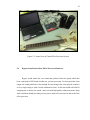
Guitar Effect Processor Design in Actual View
After all the designs for Guitar Effect Processor in Quartus II is completed, then
such as what has been discussed in Section 4.7, the design is downloaded into the FPGA
by using Quartus II programmer tool. Figure 5.5 shows the actual view of the system.
The guitar is connected to line in jacks of DE2 board, the speaker to the line out jack of
DE2 board and the laptop is connected to DE2 board by using USB blaster port.
43
Figure 5.5: Actual view of Guitar Effect Processor System
5.6
Bypass Sound from Guitar Effect Processor Hardware
Bypass sound means the raw sound that produced from the guitar which has
been connected to DE2 board and has not yet been processed. For this particular clean
output, the sound produced is clear enough for each string when it was played weather it
is for a single string or with a chord combination. Since 16-bit data width with 48k Hz
sampling rate is chosen, the sound comes out with high quality without any noise along
with it and thus should providing a more precise data to be processed in the each of the
effect processor
44
5.7
Sounds from Distortion Effect Processor Hardware
When distortion effect is selected by toggle up the assigned switch, the sound
produced becomes squeaky and fuzzy rather than clean sound of the guitar. When
playing a guitar with distortion, it is important to know how distortion affects the sound
of single notes compared to chords. Single notes will be heard clearly and the pitch of
the note played should be accurate to the instrument itself. However, chords played
through this Distortion Effect Processor will contain inter-modulated notes which may
or may not sound good. An inter-modulated note is another tone that is created by the
distortion in addition to the notes that you played. The amount or type of distortion will
determine the volume of these inter-modulated notes. For this case, there are two
different threshold parameter is provided in Distortion Effect Processor which has been
set as X"0080" and X"00FF" and for each parameter, it produces a slightly different
sound where a more squeaky and fuzzy sound is produced when parameter X”0080” is
selected. It means that lower value of threshold parameter as the clipping value will
produce more squeaky and fuzzy sound. This sounds very cool, especially when chords
are kept to a maximum of 2 or 3 notes. When chords of 6 notes are played however, the
results are usually muddy and undesirable. They may not be in tune with the chords
played and the more notes played in the chord, the more inter-modulated notes there will
be. This is what gave rise to the infamous "Power Chord". Rock bands started playing
two note chords that were an interval of a perfect 5th. For example, a G and a D, or an E
and a B. These 2-note chords, when distorted, produce an inter-modulated note that is
pleasantly in tune with the chord. However the volume strength sound produced when it
was processed in the Distortion Effect Processor became lower. To overcome this
problem, a simple gain (Volume Module) to make high of the volume is placed at the
output for each left and right channel after the Distortion Module where it resulting a
better sound after it was added.
45
5.8
Sounds from Delay Effect Processor Hardware
There are two different type of delay provided in which it takes different value
of delay buffer to be added to the input. The resulting sound for the Delay Effect
Processor of first type where when the delay_type is „0‟, the delayed sound is hardly to
be heard. Instead of that, the design is producing more high quality distortion sound.
The delay sound is hardly heard is due to the very short amount of shifted delay in the
delay buffer because the value of Reg 0 is taken to be added to input and this value has
only been shifted for once from the input. Meanwhile, when the second type where the
value of Reg 7 is taken to be added to input is selected; the delay is still hardly heard but
the output sound has become really squeaky and fuzzy more than what the Distortion
Effect Processor has produced where it is more like as we are using the metal zone
guitar effect pedal. This has resulting the sound that has really deviated from its own
purpose but instead it can give a more metal sound where most of the guitar players
really like them. The design has also been tried to take the value of Reg 10 to be mixed
as the delay flavor but it still implies the almost same result. This may be due to the
saturated output produced which keep producing absolute minimum and maximum
value where in the end the it is producing the perfect shape of square waveform.
5.9
Sounds from Both of the Effects is Activated
Given by the advantages of the chained pipeline design, we can essentially turn
on both of the effect at the same time. The resulting sound when both of the effect is
activated is that it is producing a much powerful and smooth distortion sound and
unexpectedly, it adds some more „metal‟ flavor into the distortion sound especially
when lower threshold parameter for Distortion Effect Processor was chose and the
longer delay effect was chose in Delay Effect Processor. This is because the delay effect
46
sound produced when the Delay Effect Processor alone is activated is still not giving a
good quality of delay effect, but instead it is giving a more powerful distortion sound,
thus activating it together with the Distortion Effect Processor still implies that the same
performance.
47
CHAPTER 6
CONCLUSSION AND RECOMMENDATIONS
6.1
Conclusion
The proposed Guitar Effect Processor sound system and development design is
successfully implemented in the FPGA and is a success as proved by its determined
operation which is to perform guitar‟s distortion effect and as well as delay effect.
Distortion Effect Processor gives a very good performance where it can transform the
clean guitar‟s sound into a squeaky and fuzzy sound while the Delay Effect Processor
has not much give a good performance since the effect is hardly to be heard even though
the longest delayed of the input was taken. Instead of that, it is giving a smoother and
sharper distortion sound which has more quality rather than the Distortion Effect
Processor itself. However both of the effect can still be activated at the same time and it
still can produce a different sound than one another with when only each effect is
selected alone. Even though the there are only two guitar effect pedals was implemented
in this project, it provides a good opportunity to improvise the project since the audio
CODEC is already configured rightly.
48
6.2
Problem Highlights
Getting the audio CODEC working was the critical path to the rest of the system.
In fact, it does consume a lot of time to solve this issue. It was very frustrating until that
point as I felt that all of the efforts would be worthless if that component did not work.
The issue is that even though the register of the codec has been rightfully configured by
using VHDL, it just keep giving bypass sound while I actually have disable bypass in
the register setting. This has causes the data cannot be processed into the effect
processing block. Since the time wasted on solving this problem takes too long, hence
the only option is to use the demonstration example provided by Altera where it is in
verilog and there are some modification need to be done in order to make it fit working
to the purpose of this project. Regardless about that, at the end, it has been a
successfully configured to make it work out accordingly.
Since this project is dealing with real time audio processing, it is kind of hard to
achieve and to determine the waveform produce during the design was implemented
into the DE2 board. There suppose to be a way to use the Tap Signal compiler provided
where it can take the internal data in the FPGA to generate waveform. The attempt to
use this feature is not success and the reasons for parting with this was that there were
licensing issues requirement.
6.3
Recommendations for Future Works
Well, there are a lot more rooms for improvement can be done on this project.
Since the Delay Effect Processor is not giving quite a satisfaction performance, thus the
design should be developed using another way. RAM can be use as storage to make a
function as delay buffer where it can give a better quality to make delay effect.
49
There are only two of guitar effect pedals that was implemented in this project
while there many more available types such as chorus, vibrato, flanger, tremolo and so
on can be developed and implemented. Many of them are just manipulation of delay
effect. Hence, once delay effect is working perfectly, developing the others is just a
matter of time.
To make ease of the design process, try to use DSP builder tools. Like the SOPC
builder, this tool is one of the compliment tools for Quartus II software. This tool is
intended to associate with MATLAB software where it can enable us to use the module
available in the MATLAB to do some digital signal processing. This DSP builder can
also be used to generate the VHDL code based base on the module created using
Simulink via MATLAB. While the use of the DSP builder is said to not be trivial to the
point where it requires no training, it still can be used to verify our design later on.
Since the resource on the DE2 board such as the switch is limited, it is better if a
Graphical User Interface (GUI) can be developed for this project. When more effect is
developed, it‟s going to need more switch and consequently, there will be no more left.
Hence the only option left is to develop the GUI.
It will be very good if other compliment for sound processing such as the tone
adjustment which can utilizes the uses of filter, audio equalizer and others can be
implemented in the project. This enhancement can greatly help to produce a better and
wonderful sound.
50
REFERENCES
1.
V. Menon and D.J. Levitin, “The rewards of music listening: response and
physiological connectivity of the mesolimbic system.” NeuroImage, vol. 28, pp.
175-84, 2005.
2.
P.N. Juslin, S. Liljeström, D. Västfjäll, G. Barradas, and A. Silva, “An
experience sampling study of emotional reactions to music: listener, music, and
situation,” Emotion, vol. 8, pp. 668-83, 2008.
3.
P.N. Juslin and D. Västfjäll, “Emotional responses to music: the need to consider
underlying mechanisms,” The Behavioral and Brain Sciences, vol. 31, pp. 559621, 2008.
4.
S. Saarikallio, “Music as mood regulation in adolescence,” Ph.D. dissertation,
University of Jyväskylä, Jyväskylä, Finland, 2007.
5.
T. Lesiuk, “The effect of music listening on work performance,” Psychology of
Music, vol. 33, pp. 173-191, 2005.
6.
R. E. Milliman, “Using background music to affect the behaviour of supermarket
shoppers,” The Journal of Marketing, vol. 46, No. 3, pp. 86-91, 1982.
7.
R.E. Milliman, “The influence of background music on the behavior of
restaurant patrons,” Russell The Journal Of The Bertrand Russell Archives, vol.
13, pp. 286-289, 1986.
8.
H. Ragneskog, G. Bråne, I. Karlsson and M. Kihlgren, “Influence of dinner
music on food intake and symptoms common in dementia,” Scandinavian
Kournal of Caring Sciences, vol. 10, pp. 11-47, 2010.
9.
U.Meyer-Baese. Digital Signal Processing with Field Programmable Gate
Arrays. New York: Springer-Verlag. 2004.
10.
Altera DE2 Board User Manual
11.
Altera Corporation. FPGA vs. DSP Design Reliability and Maintenance.
12.
Http://www.guitareffectspedals.com
13.
Http://www.terasic.com.tw/cgi-bin/page/archive.pl?Language=English&No=30
51
14.
Dr Mohamed Khalil Hani. “Stater‟s Guide to Digital Systems VHDL and
Verilog Design”. Universiti Teknologi Malaysia.2009
15.
Chet, C. Y. “Design and Implement of Digital Audio equalizer using
TMS320C31 system”. Master‟s Thesis. University Technology Malaysia. 1998.
16.
K.Mitra, S. Digital Signal Processing: “A Computer-based Approach”. New
York: McGraw Hill. 2006.
17.
“WM8731/WM8731L Portable Internet Audio CODEC with Headphone Driver
and Programmable Sample Rates”, Wolfson Microelectronics Production
Datasheet. Rev 4.0, February 2005.
18.
A.R.M. Khan, A.P.Thakare, S.M.Gulhane. ”FPGA-Based Design of Controller
for Sound Fetching from Codec Using Altera DE2 Board”. International Journal
of Scientific & Engineering Research, Volume 1, Issue 2, November-2010.
19.
Tomasz Kaczmarczyk, Tomasz Henisz, Dominik Stożek. DGN-1 Digital Guitar
Effects Processor, Revision 1 Feature overview and basic technical
documentation.
.
52
APPENDIX A
VERILOG CODE OF WM8731 CONTROL
---------------------------------------------------------------------------------------------------------// Copyright (c) 2005 by Terasic Technologies Inc.
// -------------------------------------------------------------------------------------------------------// Major Functions: I2C output data
// -------------------------------------------------------------------------------------------------------// Revision History :
// -------------------------------------------------------------------------------------------------------// Ver :| Author
// V1.0 :| Joe Yang
:| Mod. Date :| Changes Made:
:| 05/07/10 :|
Initial Revision
// --------------------------------------------------------------------------------------------------------
`define rom_size 6'd8
module CLOCK_500 (
CLOCK,
CLOCK_500,
DATA,
END,
RESET,
GO,
CLOCK_2
53
);
input CLOCK;
input END;
input RESET;
output CLOCK_500;
output [23:0]DATA;
output GO;
output CLOCK_2;
reg [10:0]COUNTER_500;
wire CLOCK_500=COUNTER_500[9];
wire CLOCK_2=COUNTER_500[1];
reg [15:0]ROM[`rom_size:0];
reg [15:0]DATA_A;
reg [5:0]address;
wire [23:0]DATA={8'h34,DATA_A};
// Main address for WM8731 with 2 wire
MPU serial interface, CBS is tied to the ground.
wire GO =((address <= `rom_size) && (END==1))? COUNTER_500[10]:1;
always @(negedge RESET or posedge END) begin
if (!RESET) address=0;
else
if (address <= `rom_size) address=address+1;
end
reg [7:0]vol;
always @(posedge RESET) begin
54
vol=vol-1;end
always @(posedge END) begin
//
ROM[0]= 16'h1e00;
ROM[0]= 16'h0c00;
//Power Down Control : Power down
ROM[1]= 16'h0ec2;
//Digital audio Format Interface : left
//justified,16 bit,master mode,invert BCLK
ROM[2]= 16'h0812;
//Analogue Audio Path Control : Disable
//bypass,Line-in select,DAC select
ROM[8]= 16'h0a06;
//Digital Audio Path Control : 48kHz
//deemphasizes
ROM[3]= 16'h1000;
//Sampling Control : Normal mode,mclk =
//18.43Mhz
ROM[4]= 16'h0017;
//Left Line In : Disable mute
ROM[5]= 16'h0217;
//Right Line In : Disable mute
ROM[6]= {8'h04,1'b0,vol[6:0]};
//Left Headhone Out : sound vol
ROM[7]= {8'h06,1'b0,vol[6:0]};
//Right Headphone Out : sound vol
//ROM[4]= 16'h1e00;
//reset
ROM[`rom_size]= 16'h1201;//active
DATA_A=ROM[address];
end
always @(posedge CLOCK ) begin
COUNTER_500=COUNTER_500+1;
end
endmodule
55
---------------------------------------------------------------------------------------------------------// Copyright (c) 2005 by Terasic Technologies Inc.
// -------------------------------------------------------------------------------------------------------// Major Functions:i2c controller
// -------------------------------------------------------------------------------------------------------// Revision History :
// -------------------------------------------------------------------------------------------------------// Ver :| Author
:| Mod. Date :| Changes Made:
// V1.0 :| Joe Yang
:| 05/07/10 :|
Initial Revision
----------------------------------------------------------------------------------------------------------
module de2_i2c_controller (
CLOCK,
I2C_SCLK,
// I2C CLOCK
I2C_SDAT,
// I2C DATA
I2C_DATA, // DATA:[SLAVE_ADDR,SUB_ADDR,DATA]
GO,
// GO transfor
END,
// END transfor
W_R,
// W_R
ACK,
// ACK
RESET,
// TEST
SD_COUNTER,
SDO
);
input CLOCK;
input [23:0] I2C_DATA;
input GO;
input RESET;
input W_R;
56
inout I2C_SDAT;
output I2C_SCLK;
output END;
output ACK;
// TEST
output [5:0] SD_COUNTER;
output SDO;
reg SDO;
reg SCLK;
reg END;
reg [23:0] SD;
reg [5:0] SD_COUNTER;
wire I2C_SCLK = SCLK | (((SD_COUNTER >= 4) & (SD_COUNTER <= 30))?
~CLOCK : 0);
wire I2C_SDAT = SDO ? 1'bz : 0;
reg ACK1, ACK2, ACK3;
wire ACK = ACK1 | ACK2 | ACK3;
//--I2C COUNTER
always @(negedge RESET or posedge CLOCK)
begin
if (!RESET)
SD_COUNTER = 6'b111111;
else
begin
if (GO == 0)
57
SD_COUNTER = 0;
else
if (SD_COUNTER < 6'b111111)
SD_COUNTER = SD_COUNTER + 1;
end
end
always @(negedge RESET or posedge CLOCK )
begin
if (!RESET)
begin
SCLK = 1;
SDO = 1;
ACK1 = 0;
ACK2 = 0;
ACK3 = 0;
END = 1;
end
else
case (SD_COUNTER)
6'd0 : begin ACK1 = 0; ACK2 = 0; ACK3 = 0; END = 0; SDO = 1; SCLK = 1; end
// Start
6'd1 : begin SD = I2C_DATA; SDO = 0; end
6'd2 : SCLK = 0;
// Slave Address for WM8731
6'd3 : SDO = SD[23];
6'd4 : SDO = SD[22];
6'd5 : SDO = SD[21];
6'd6 : SDO = SD[20];
58
6'd7 : SDO = SD[19];
6'd8 : SDO = SD[18];
6'd9 : SDO = SD[17];
6'd10 : SDO = SD[16];
6'd11 : SDO = 1'b1; //ACK
// Sub-address for WM8731 control register Map
6'd12 : begin SDO = SD[15]; ACK1 = I2C_SDAT; end
6'd13 : SDO = SD[14];
6'd14 : SDO = SD[13];
6'd15 : SDO = SD[12];
6'd16 : SDO = SD[11];
6'd17 : SDO = SD[10];
6'd18 : SDO = SD[9];
6'd19 : SDO = SD[8];
6'd20 : SDO = 1'b1; // ACK
// Data for WM8731 control data register
6'd21 : begin SDO = SD[7]; ACK2 = I2C_SDAT; end
6'd22 : SDO = SD[6];
6'd23 : SDO = SD[5];
6'd24 : SDO = SD[4];
6'd25 : SDO = SD[3];
6'd26 : SDO = SD[2];
6'd27 : SDO = SD[1];
6'd28 : SDO = SD[0];
6'd29 : SDO = 1'b1; // ACK
// Stop
6'd30 : begin SDO = 1'b0; SCLK = 1'b0; ACK3 = I2C_SDAT; end
6'd31 : SCLK = 1'b1;
59
6'd32 : begin SDO = 1'b1; END = 1; end
endcase
end
endmodule
60
APPENDIX B
VHDL CODE OF GUITAR EFFECT PROCESSOR
------------------------------------simple register with low reset-----------------------------------
library ieee;
use ieee.std_logic_1164.all;
use ieee.std_logic_arith.all;
use ieee.std_logic_unsigned.all;
entity reg is port (
clk,rst : in std_logic;
parameter : in std_logic_vector (15 downto 0);
output : buffer std_logic_vector(15 downto 0));
end reg;
architecture arch of reg is begin
process (clk,rst,output) begin
if rst='0' then output <= (others => '0');
elsif clk'event and clk ='1' then
output <= parameter;
else output<= output;
end if;
61
end process;
end arch;
--------------------------------------------Comparator-----------------------------------------------
library ieee;
use ieee.std_logic_1164.all;
use ieee.std_logic_signed.all;
entity comparatorGt is port (
sample : in std_logic_vector(15 downto 0);
parameter : in std_logic_vector(15 downto 0);
Gt : out std_logic );
end comparatorGt;
architecture behave of comparatorGt is begin
Gt <= '1' when sample>parameter else '0';
end behave;
---------------------------------------------Sign Converter-------------------------------------------
library ieee;
use ieee.std_logic_1164.all;
use ieee.std_logic_arith.all;
use ieee.std_logic_signed.all;
entity convert is port ( inparameter : in std_logic_vector(15 downto 0);
outparameter : out std_logic_vector(15 downto 0));
end convert;
62
architecture behave of convert is begin
outparameter <= -inparameter ;
end behave;
-----------------------------------------Mux 2to1 Selector-------------------------------------------
library ieee;
use ieee.std_logic_1164.all;
use ieee.std_logic_signed.all;
entity mux2to1 is port ( sample , parameter : in std_logic_vector(15 downto 0);
sel : in std_logic;
outmux : out std_logic_vector (15 downto 0));
end mux2to1;
architecture behave of mux2to1 is begin
process (sample ,parameter,sel) begin
if sel='1' then outmux <= parameter;
else outmux <= sample;
end if;
end process;
end behave;
63
-----------------------------------------Distortion Module--------------------------------------------This module is achieved by using port map style which taking parts if other module
---------------------------------------------------------------------------------------------------------
library ieee;
use ieee.std_logic_1164.all;
use ieee.std_logic_arith.all;
use ieee.std_logic_signed.all;
entity distortion is port ( clk : in std_logic;
rst : in std_logic;
sample : in std_logic_vector(15 downto 0);
parameter1 : in std_logic_vector (15 downto 0);
distorted : out std_logic_vector (15 downto 0));
end distortion;
architecture arch of distortion is
signal reg1 : std_logic_vector(15 downto 0);
signal conversion : std_logic_vector (15 downto 0);
signal compare1 : std_logic ;
signal mux1 : std_logic_vector (15 downto 0);
signal compare2 : std_logic ;
component reg port ( clk,rst : in std_logic;
parameter : in std_logic_vector (15 downto 0);
output : buffer std_logic_vector(15 downto 0));
end component;
component comparatorGt port ( sample : in std_logic_vector(15 downto 0);
parameter : in std_logic_vector(15 downto 0);
64
Gt : out std_logic );
end component;
component mux2to1 is port ( sample , parameter : in std_logic_vector(15 downto 0);
sel : in std_logic;
outmux : out std_logic_vector (15 downto 0));
end component;
component convert is port ( inparameter : in std_logic_vector(15 downto 0);
outparameter : out std_logic_vector(15 downto 0));
end component;
begin
s1 : reg port map ( clk, rst, parameter1, reg1);
s2 : comparatorGt port map (sample, reg1,compare1);
s3 : mux2to1 port map (sample, reg1,compare1, mux1);
s4 : convert port map (reg1,conversion);
s5 : comparatorGt port map (mux1, conversion, compare2);
s6 : mux2to1 port map (conversion, mux1, compare2,distorted);
end arch;
----------------------------------------------Delay Module-------------------------------------------
library IEEE;
use IEEE.std_logic_1164.all;
use IEEE.std_logic_unsigned.all;
entity delay_echo is port (
65
--data control
delay_enable: in std_logic;
delay_type : in std_logic;
--data
sample_in: in std_logic_vector(15 downto 0);
decay : in std_logic_vector (7 downto 0);
sample_out : out STD_LOGIC_VECTOR(15 downto 0)
);
end delay_echo;
architecture beh of delay_echo is
signal dataIn : std_logic_vector(15 downto 0);
signal delay_multiplied : std_logic_vector(24 downto 0);
signal dm: std_logic;
signal output_sat: std_logic_vector(16 downto 0);
type myarray is array (INTEGER range <>) of std_logic_vector(15 downto 0);
signal delay_Buffer : myarray (9 downto 0);
begin
process (sample_in,delay_enable,delay_Buffer)
begin
-- select delay_enable to do delay buffer
if delay_enable <= '1' then
-- delay 10 clock cycles
delay_Buffer(0) <= delay_Buffer(1);
delay_Buffer(1) <= delay_Buffer(2);
delay_Buffer(2) <= delay_Buffer(3);
delay_Buffer(3) <= delay_Buffer(4);
66
delay_Buffer(4) <= delay_Buffer(5);
delay_Buffer(5) <= delay_Buffer(6);
delay_Buffer(6) <= delay_Buffer(7);
delay_Buffer(7) <= delay_Buffer(8);
delay_Buffer(8) <= delay_Buffer(9);
delay_Buffer(9) <= sample_in
else
dataIn <= sample_in;
end if;
end process;
process(delay_type,delay_Buffer,output_sat,dm,sample_in,delay_multiplied,decay)
begin
if delay_type <= '0' then
--Calculate the echo after decay,taking the internal delay buffer of 0
delay_multiplied <= delay_Buffer(0) * ('0' & decay);
--Duplicate the topmost bit to use for overflow detetction
dm <= delay_multiplied(24);
output_sat <= (dm & delay_multiplied(24 downto 9)) +
(sample_in(15) & sample_in);
if output_sat(16 downto 15) = "01" then dataIn <=
"0111111111111111"; elsif
output_sat(16 downto 15) = "10" then dataIn <=
"1000000000000000"; else
dataIn <= output_sat(15 downto 0);
end if;
else
--Calculate the echo after decay,taking the internal delay buffer of 7
delay_multiplied <= delay_Buffer(7) * ('0' & decay);
67
--Duplicate the topmost bit to use for overflow detetction
dm <= delay_multiplied(24);
output_sat <= (dm & delay_multiplied(24 downto 9)) +
(sample_in(15) & sample_in);
-- decay is 1/2
if output_sat(16 downto 15) = "01" then dataIn <=
"0111111111111111"; elsif
output_sat(16 downto 15) = "10" then dataIn <=
"1000000000000000"; else
dataIn <= output_sat(15 downto 0);
end if;
end if;
end process;
-- changes data precision of playback data.
sample_out <= dataIn; -- 16 bits precision
end beh;
-----------------------------------------------Bypass---------------------------------------------------bypass.vhd
--A simple switch enabling to bypass an effect
----------------------------------------------------------------------------------------------------------
library IEEE;
use IEEE.std_logic_1164.all;
entity bypass is
port (
--signal not transformed by the effect
sample_in_left: in std_logic_vector(15 downto 0);
sample_in_right: in std_logic_vector(15 downto 0);
68
--signal transformed by the effect
device_in_left: in std_logic_vector(15 downto 0);
device_in_right: in std_logic_vector(15 downto 0);
--output
sample_out_left: out std_logic_vector(15 downto 0);
sample_out_right: out std_logic_vector(15 downto 0);
bypass: in std_logic );
end entity bypass;
architecture behave of bypass is
begin
sample_out_left <= sample_in_left when bypass = '0' else device_in_left;
sample_out_right <= sample_in_right when bypass = '0' else device_in_right;
end architecture behave;
----------------------------------------------Pipeline Buffer-------------------------------------------pipeline_buffer.vhd
--A simple pipeline buffer for two 16bit channels
----------------------------------------------------------------------------------------------------------
library IEEE;
use IEEE.std_logic_1164.all;
entity pipeline_buffer is
port (
clk: in std_logic;
reset: in std_logic;
-- data
sample_in_left: in std_logic_vector(15 downto 0);
69
sample_out_left: out std_logic_vector(15 downto 0);
sample_in_right: in std_logic_vector(15 downto 0);
sample_out_right: out std_logic_vector(15 downto 0)
);
end entity pipeline_buffer;
architecture behave of pipeline_buffer is
signal last_lrclk: std_logic;
begin
process (clk, reset)
begin
if (reset='0') then
sample_out_right <= (others => '0');
sample_out_left <= (others => '0');
elsif rising_edge(clk) then
sample_out_right <= sample_in_right;
sample_out_left <= sample_in_left;
end if;
end process;
end architecture behave;
-------------------------------------------Volume Module---------------------------------------------volume.vhd
--A simple digital amplifier with overflow control. It multiplies the input signal by
volume/512. Overflows are caught and result in the saturation of the amplifier.
----------------------------------------------------------------------------------------------------------
library IEEE;
use IEEE.std_logic_1164.all;
use ieee.std_logic_arith.all;
70
use ieee.std_logic_signed.all;
entity volume is
port (
-- data
sample_in: in std_logic_vector(15 downto 0);
sample_out: out std_logic_vector(15 downto 0);
-- params
parameter: in std_logic_vector(15 downto 0)
);
end entity volume;
architecture beh of volume is
signal signal_unnormalized: std_logic_vector(31 downto 0);
begin
signal_unnormalized <= sample_in * parameter;
normalize_saturate: process(signal_unnormalized)
begin
if (signal_unnormalized(31) = '1') then -- result negative
if (signal_unnormalized(30 downto 23) = "11111111") then
-- no overflow
sample_out <= '1' & signal_unnormalized(22 downto 8);
else
-- overflow negative
sample_out <= "1000000000000000";
end if;
else -- result positive
if (signal_unnormalized(30 downto 23) = "00000000") then
-- no overflow
sample_out <= '0' & signal_unnormalized(22 downto 8);
else
-- overflow positive
71
sample_out <= "0111111111111111";
end if;
end if;
end process;
end architecture beh;
-------------------------------------------Audio Deserializer----------------------------------------- -------------------------------------------------------------------------------------------------------- Audio - buffer . Receives seriel data from ADC , 32 bits including both --- channels , and transmitts 2x16 bit packages , left channel --- first , in parallel at the output . --- -------------------------------------------------------------------------------------------------------
library ieee ;
use ieee . std_logic_1164 .all ;
entity Audio_DeserializeR is
port (
--clock and adc data care
reset : in std_logic ;
bclk : in std_logic ;
lrck : in std_logic ;
adc_data : in std_logic ;
--adc audio buffered to 16 bit each channel
left_word : out std_logic_vector (15 downto 0);
right_word : out std_logic_vector (15 downto 0)
);
end entity Audio_DeserializeR ;
architecture structure of Audio_DeserializeR is
72
type state is (IDLE , RECEIVE , TRANSFER_LEFT , TRANSFER_RIGHT );
signal next_state : state ;
signal audio_data : std_logic_vector (31 downto 0); --Audio - data storage
signal counter : integer range 31 downto 0 := 31;
begin
FSM : process (bclk , reset )
begin
-- Initial configuration of buffer
if( reset = '0') then
next_state <= IDLE ;
left_word <= ( OTHERS => '0');
right_word <= ( OTHERS => '0');
audio_data <= ( OTHERS => '0');
elsif ( rising_edge (bclk )) then
case next_state is
--IDLE state
when IDLE =>
--Codec transfers data from ADC
if( lrck = '1') then
next_state <= RECEIVE ;
elsif (lrck = '0') then
next_state <= IDLE ;
end if;
--Receive data from both channels , left channel first
when RECEIVE =>
if( counter > 0) then
73
audio_data ( counter ) <= adc_data ;
--Saves audio data
counter <= counter - 1;
next_state <= RECEIVE ;
else
audio_data ( counter ) <= adc_data ;
counter <= 31;
next_state <= TRANSFER_LEFT ;
end if;
--Puts left channel data on the parallel output
when TRANSFER_LEFT =>
left_word (15 downto 0) <= audio_data (31 downto 16);
next_state <= TRANSFER_RIGHT ;
--Puts right channel data on the parallel output
when TRANSFER_RIGHT =>
right_word (15 downto 0) <= audio_data (15 downto 0);
next_state <= IDLE ;
end case ;
end if;
end process ;
end architecture ;
--------------------------------------------Mono Selector---------------------------------------------mono_selector.vhd
--Since guitar input is usually a mono signal with the right channel left silent, this
--module can be used to feed both channels from the left channel input.
----------------------------------------------------------------------------------------------------------
library IEEE;
74
use IEEE.std_logic_1164.all;
entity mono_selector is
port (
-- data
sample_in_left: in std_logic_vector(15 downto 0);
sample_in_right: in std_logic_vector(15 downto 0);
sample_out_left: out std_logic_vector(15 downto 0);
sample_out_right: out std_logic_vector(15 downto 0);
-- params
mono: in std_logic
);
end entity mono_selector;
architecture beh of mono_selector is
begin
sample_out_right <= sample_in_right when mono = '0' else sample_in_left;
sample_out_left <= sample_in_left;
end architecture beh;
------------------------------------------Audio Serializer--------------------------------------------
----------------------------------------------------------------------------------------------------------- Audio output buffer . Receives 2 x 24 bit parallel data packages --- from filter , and puts 32 bits of serial data to the output when --- audio - codec is ready to receive . -----------------------------------------------------------------------------------------------------------
library ieee ;
use ieee . std_logic_1164 .all ;
75
entity Audio_SerializeR is
port
(
--clock care
reset : in std_logic ;
bclk : in std_logic ;
lrck : in std_logic ;
--sample to be serialized
left_word : in std_logic_vector (15 downto 0);
right_word : in std_logic_vector (15 downto 0);
--dac data output
dac_data : out std_logic -- Output to the audio - codec
);
end entity Audio_SerializeR ;
architecture structure of Audio_SerializeR is
type state is (IDLE , RECEIVE_RIGHT , START_TRANSFER ,
CONT_TRANSFER );
signal next_state : state ;
signal audio_data : std_logic_vector (31 downto 0);
signal counter : integer range 31 downto 0 := 31;
begin
FSM : process (bclk , reset )
begin
-- Initial configuration of output buffer
if( reset = '0') then
next_state <= IDLE ;
dac_data <= '0';
audio_data (31 downto 0) <= ( OTHERS => '0');
76
elsif ( rising_edge (bclk )) then
case next_state is
--IDLE state
when IDLE =>
--Save data for left channel on the 16 MSBs
audio_data (31 downto 16) <= left_word (15 downto 0);
next_state <= RECEIVE_RIGHT ;
-- Receive and save data (24 bit) for right channel
when RECEIVE_RIGHT =>
audio_data (15 downto 0) <= right_word (15 downto 0);
next_state <= START_TRANSFER ;
-- Transmits the MSB to audio - codec when codec is ready
when START_TRANSFER =>
if (lrck = '1') then --When DAC is ready
--MSB left channel
dac_data <= audio_data ( counter );
counter <= counter - 1;
next_state <= CONT_TRANSFER ;
elsif (lrck = '0') then
next_state <= START_TRANSFER ;
end if;
--Sends the rest of the audio data to the codec in serial
when CONT_TRANSFER =>
if( counter > 0) then
dac_data <= audio_data ( counter );
counter <= counter - 1;
next_state <= CONT_TRANSFER ;
77
else
dac_data <= audio_data ( counter );
counter <= 31;
next_state <= IDLE ;
end if;
end case ;
end if;
end process ;
end architecture ;