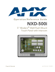
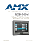
1
TITLE
THE DESIGN AND REALISATION OF AN
FPGA BASED AUDIO PROCESSOR
STUDENT
MIKE HUDSON 18022224
PROJECT
DR. JOHN HOLDING
SUPERVISOR
COURSE
BENG HON ELECTRICAL AND
ELECTRONIC ENGINEERING
([email protected])
9/05/2012
Mike Hudson
Preface
This report describes project work carried out within the Engineering Programme at
Sheffield Hallam University from October 2011 to April 2012.
The submission of the report is in accordance with the requirements for the award of the
degree of “Bachelor of Electrical and Electronic Engineering with Honours” under the
auspices of the University.
II
Mike Hudson
Acknowledgements
I would like to thank my supervisor Dr John Holding for his advice and guidance
throughout the duration of this project. I would also like to thank every one who has
helped me over at the Altera Internet forums.
III
Mike Hudson
Abstract
This project report documents the use of a field programmable gate array (FPGA) for
real-time processing of audio. The traditional software approach to digital signal
processing often introduces an unacceptable delay between the audio input and the audio
output (referred to as the total system latency). This can be problematic for applications
that require real-time operation such as live processing of musical instruments. An
FPGA design allows the same software routines to be implemented as hardware,
therefore eliminating high system latency and potential unreliability.
Quartus II v11.0 and SOPC Builder have been used to design and create the VHDL code
to be synthesised. The implementation of the VHDL design uses the DE2 development
board from Altera which is based around a Cyclone EP2C35 FPGA device having 35000
logic elements.
Four audio effects were explored and implemented: echo, flanger, filter and reverb.
External control to the FPGA was implemented using rotary encoders to change various
effect parameters, and visual feedback been given through an LCD. The final design
utilises a Nois II soft-core processor to form part of the user interface. The results show
that the total system latency of the FPGA audio processor was considerably less than a
computer software application: less than 1ms compared to 10ms.
The initial concept has been proven using a total of 11702 logic elements. There is
much scope for development of the final project. Future work could focus of a more
user-friendly system in terms of the user interface and also the creation of more
advanced audio effects.
IV
Mike Hudson
Table of contents
Preface .......................................................................................................................................... II Acknowledgements ...................................................................................................................... III Abstract ........................................................................................................................................ IV Table of contents .......................................................................................................................... .V
Nomenclature and abbreviations ............................................................................................. VIII Table of Figures .......................................................................................................................... IX
1 Introduction ............................................................................................................................ 1 1.1 Digital audio processing ................................................................................................... 1 1.2 Project aims and objectives .............................................................................................. 2 1.1 Previous works and current products ............................................................................... 3 2 Background and Theory ....................................................................................................... 5 2.1 Background....................................................................................................................... 5 2.2 Digital audio theory .......................................................................................................... 5 2.3 The building blocks of basic audio effects ....................................................................... 7 2.4 Digital filter example ........................................................................................................ 8 2.5 Conclusion ........................................................................................................................ 8 3 Approach .............................................................................................................................. 10 3.1 General ........................................................................................................................... 10 3.2 Selection of Tools and Software..................................................................................... 10 4 The Altera DE2 development board .................................................................................. 12 4.1 Features........................................................................................................................... 12 5 Altera Quartus II ................................................................................................................. 14 5.1 Introduction .................................................................................................................... 14 5.2 SOPC Builder ................................................................................................................. 14 6 Interfacing Audio to the audio to the FPGA ..................................................................... 16 6.1 The Wolfson WM8781 audio ADC ............................................................................... 16 6.2 Configuration .................................................................................................................. 18 6.2.1 Sampling frequency ................................................................................................ 20 6.2.2 Register map............................................................................................................ 20 V
Mike Hudson
6.3 Serial/parallel conversion ............................................................................................... 21 6.1 Digital serial data stream ................................................................................................ 24 6.2 Summary......................................................................................................................... 24 7 Building a project library of Quartus block symbols ....................................................... 25 7.1 Multiply .......................................................................................................................... 25 7.2 Sum ................................................................................................................................. 25 7.3 Mixer .............................................................................................................................. 26 7.4 Small delay-line in hardware .......................................................................................... 27 7.5 Summary......................................................................................................................... 28 8 Implementing a buffer in RAM .......................................................................................... 29 8.1 Requirements .................................................................................................................. 29 8.2 Choice of RAM device ................................................................................................... 29 8.3 SDRAM controller Core................................................................................................. 29 8.4 Reading/writing to and from the SDRAM ..................................................................... 30 8.5 RAM state machine ........................................................................................................ 32 8.6 Implementation of a circular buffer ................................................................................ 34 8.7 Multiple read pointers..................................................................................................... 36 8.8 Multiple buffer instances ................................................................................................ 36 8.9 Summary......................................................................................................................... 37 9 Echo effect ............................................................................................................................ 39 9.1 Implementation ............................................................................................................... 39 10 Audio filter .......................................................................................................................... 41 10.1 State variable filter ....................................................................................................... 41 10.2 Discussion..................................................................................................................... 43 11 Flanger effect ...................................................................................................................... 44 12 Reverberation effect........................................................................................................... 46 12.1 A basic reverb ............................................................................................................... 46 12.2 The all-pass filter .......................................................................................................... 46 12.2.1 Multiple all-pass filters ......................................................................................... 48 12.3 Impulse response test .................................................................................................... 48 12.4 Comparison with a commercial software reverb .......................................................... 51 12.5 Summary....................................................................................................................... 54 VI
Mike Hudson
13 Latency test ......................................................................................................................... 56 13.1 Comparison with computer software............................................................................ 56 13.2 Summary....................................................................................................................... 57 14 User Interface ..................................................................................................................... 59 14.1 Considerations .............................................................................................................. 59 14.2 Quadrature rotary encoder ............................................................................................ 60 14.3 Interfacing the controls ................................................................................................. 62 14.4 Visual feedback ............................................................................................................ 62 14.5 Discussion and summary .............................................................................................. 64 15 Conclusion .......................................................................................................................... 65 15.1 Further work ................................................................................................................. 65 16 References ........................................................................................................................... 67 17 Appendices .......................................................................................................................... 69 17.1 Quartus II screenshots .................................................................................................. 69 17.2 Project photographs ...................................................................................................... 70 VII
Mike Hudson
Nomenclature and abbreviations
ADC
Analogue to Digital Converter
AIFF
Audio Interchange File Format
CODEC Refers to audio ADC/DAC device
DAC
Digital to Analogue Converter
DE2
Refers to the Altera Development and Education board
DSP
Digital Signal Processor
FIR
Finite Impulse Response
FPGA
Field Programmable Gate Array
HDL
Hardware Description Language
I2 C
Inter-Integrated Circuit Serial Protocol
IC
Integrated Circuit
IDE
Integrated development Environment
IEEE
Institute of Electrical and Electronics Engineers
IP
Intellectual property
LSB
Least Significant Bit
MAC
Multiply Accumulate
MSB
Most Significant Bit
PISO
Parallel In Serial Out
PLL
Phase Locked Loop
SIPO
Serial In Parallel Out
SOPC
System On Programmable Chip
VHDL
VHSIC Hardware Description Language
VIII
Mike Hudson
Table of Figures
Figure 2-1: (a) An analogue signal (b) Digitised PCM signal (c) Digitised PCM signal
with fewer bits of precision (Katz. D & Gentile R, 2009) ......................................... 6 Figure 2-2: Digital audio processor example- volume (Udo Zolzer.) ................................ 6 Figure 2-3: Circular buffer concept.................................................................................... 7 Figure 2-4: Parallel FPGA FIR filter structure (Maxfield. C, 2006) ................................. 8 Figure 4-1: The Altera DE2 inputs and outputs (Altera DE2 manual) ............................ 12 Figure 6-1: Audio codec schematic (Altera DE2 User manual) ...................................... 17 Figure 6-2: left justified format (WM8781 datasheet) ..................................................... 19 Figure 6-3: Master mode (WM8731 datasheet) ............................................................... 20 Figure 6-4: WM8731 register map (WM8731 datasheet) ................................................ 21 Figure 6-5: Digital audio stream into the FPGA .............................................................. 22 Figure 6-6: Codec waveforms .......................................................................................... 23 Figure 6-7: Serial to parallel ............................................................................................ 23 Figure 6-8: Parallel to serial ............................................................................................. 23 Figure 6-9: Digital audio interfaced to the FPGA ............................................................ 24 Figure 7-1: Dry/wet ratio control of affected and original signal .................................... 26 Figure 7-2: Wet/dry ratio block symbol in Quartus ......................................................... 27 Figure 7-3: Delay-line simulation in Quartus simulator .................................................. 28 Figure 8-1: SDRAM Controller with Avalon interface block diagram (Altera Embedded
Peripherals IP User Guide)....................................................................................... 30 Figure 8-2: SOPC Builder custom component signals .................................................... 31 Figure 8-3: Component connection to the SDRAM Controller in SOPC Builder ........... 31 Figure 8-4: System top level connections in Quartus ...................................................... 31 Figure 8-5: Read and write waveforms for Avalon memory mapped master .................. 32 Figure 8-6: State Machine for a RAM Buffer .................................................................. 32 Figure 8-7: SDRAM state machine connected to SOPC System ..................................... 34 Figure 8-8: Problem with circular buffer ......................................................................... 35 Figure 8-9: Multiple read pointers in the RAM state machine ........................................ 36 Figure 8-10: Multiple SDRAM buffer components in SOPC Builder ............................. 37 IX
Mike Hudson
Figure 9-1: Variable delay ............................................................................................... 39 Figure 9-2: Variable delay feedback ................................................................................ 39 Figure 9-3: Delay effect symbol on top level in Quartus ................................................. 40 Figure 10-1: State variable filter ...................................................................................... 41 Figure 10-2: Low pass filter on the DE2 (fc = 500hz) ..................................................... 43 Figure 11-1: Flanger diagram in Matlab Simulink .......................................................... 44 Figure 11-2: Flanger effect on the DE2 ........................................................................... 45 Figure 11-3: Original signal mixed with a ten sample delayed version ........................... 45 Figure 12-1: Comb filter .................................................................................................. 46 Figure 12-2: All-pass filter ............................................................................................... 47 Figure 12-3: An all-pass filter in Simulink ...................................................................... 47 Figure 12-4: All-pass filter in Quartus II ......................................................................... 47 Figure 12-5: Multiple series all-pass reverb..................................................................... 48 Figure 12-6: Sine wave logarithmic sweep test signal ..................................................... 49 Figure 12-7: One all-pass filter 20ms delay time and 0.7 gain ........................................ 50 Figure 12-8: Three series all-pass filters on the DE2 (setting one).................................. 50 Figure 12-9: Three series all-pass filters on the DE2 (setting two) ................................. 51 Figure 12-10: Averb reverb in Logic Pro ......................................................................... 52 Figure 12-11: Averb setting one ...................................................................................... 53 Figure 12-12: Averb setting two ...................................................................................... 53 Figure 13-1: Series effect chain ....................................................................................... 56 Figure 13-2: Latency test setup ........................................................................................ 56 Figure 13-3: DE2 total system latency at 48kHz ............................................................. 57 Figure 13-4: Logic Pro total system latency at 48khz...................................................... 57 Figure 14-1: Quadrature encoder outputs ........................................................................ 60 Figure 14-2: Quadrature encoder connections to the DE2 GPIO header ......................... 60 Figure 14-3: Simulation of quadrature encoder VHDL code........................................... 61 Figure 14-4: Construction of the rotary control box ........................................................ 61 Figure 14-5: Eight rotary controls and 10 LEDS ............................................................. 61 Figure 14-6: All eight encoder connected on the top level in Quartus ............................ 62 Figure 14-7: LCD when no effect has been selected ....................................................... 63 X
Mike Hudson
Figure 14-8: Reverb effect selected- placement of text corresponds to a rotary encoder 64 Figure 17-1: Control box .................................................................................................. 70 Figure 17-2: Control input via GPIO on DE2 board ........................................................ 70 Figure 17-3: Testing the audio effects ............................................................................. 71 Figure 17-4: Apple’s impulse response utility and the Logic Pro computer software..... 71 XI
Mike Hudson
1
Introduction
1.1
Digital audio processing
Digital audio processing offers a huge amount of flexibility and an almost infinite
amount of possibility to manipulate and process audio in a way that would not be
possible using analogue techniques. In the last two decades or so, the music studio has
evolved drastically from consisting of predominantly analogue equipment to nearly all
digital equipment, based around a computer or ‘digital audio workstation’. A traditional
recording studio would have several rooms full of analogue hardware, mixers, effects
units and huge multi-track recorders using magnetic tape. An enthusiastic technician
may spend days going through their huge repository of equipment to find the perfect
reverb effect for a recording.
With the development of digital signal processing (DSP) and computer processing
power increasing at an exponential rate, it has become possible to have all those
analogue reverb units and amplifiers emulated in software on even the most modest of
personal computers using the click of a computer mouse to audition each of them. The
introduction of Steinberg’s Virtual Studio Technology (VST) in 1996 played a key role
in allowing this to happen.
This significant development has paved way for completely new instruments and made
musicians and technicians look at making music in a different way spawning hundreds
of new music genres. The last decade of music provides a good (audible) example of
how the development of technology directly influences music.
The underlying concepts and theory of DSP may not have changed much, but the
technology on which they are implemented continues to develop at a phenomenal rate.
The change in embedded multimedia processing technology has demonstrated
(especially in the last decade) how fast the technology is moving. However, as the need
for higher speed, lower cost and smaller size increases, demanding digital processing
applications are beginning to see the limitations of traditional sequential instruction DSP
processors.
1
Mike Hudson
Although not new technology, FPGAs are starting to be used more and more to
overcome the limitations of general purpose DSPs in applications where low latency is
critical.
1.2
Project aims and objectives
The aim of this project is to create a real-time, digital audio processor using an FPGA to
overcome the problems with latency experienced with traditional computer software.
Along the way, comparisons will be made, discussing advantages and disadvantages of
related technology and development tools.
The initial requirements and proposed outcomes were established:
• A minimum of 44.1kHz with minimum 16 bit sample depth
• Real-time line in and out audio
• A platform which can be used to further develop and implement audio
processing effects
• A selection of digital audio effects
• User controllable parameters via a software interface- preferably in real time
• Re-routable effects
• User feedback of parameters and selections
The project will be targeted at CD quality audio: two channel stereo, with a sample rate
of 44.1kHz and bit depth of 16 bits. The quality should also be acceptable for the
processing of an electric guitar audio signal. For audio processing of instruments and
voice, a real-time response of the audio processor is desired in order to minimise and
potentially completely eradicate perceivable delay between the input and the output
signals. A typical delay value (also referred to as system latency) on a computer
software implementation of an audio processor may be in the region of around 10ms.
Therefore an acceptable result would be a latency of less than 10ms of latency on an
2
Mike Hudson
FPGA.
A short-list of effects was created. Each of these effects require a different functionality
in a digital processing system and would also demonstrate a degree of flexibility in
terms of what can be created. In other words, the choices of effects were carefully
chosen in order to prove a concept. The idea being, that if these effects can be
successfully implemented then almost any audio effect can be created.
The proposed digital audio effects:
• Echo – requires a relatively large buffer size (at least one second)
• Flanger – requires the ability to modulate a delay value in real-time
• Filter – requires only very small fixed sample delays
• Reverb – requires multiple buffer instances and read pointers
The effects should be selectable and parameters of each audio effect should be
controllable via user input.
1.1
Previous works and current products
Recent years has seen an increase in the use of FPGAs being used for high audio
equipment that require truly parallel operations on multiple channels whilst maintaining
ultra low latency. An example of this is Euphonix choice to use the Altera Cyclone
FPGAs in their high-end audio mixing consoles.
There have been a number previous projects regarding audio processing on an FPGA.
Khan et al. (2010) demonstrated their FPGA based design of an I2C controller for
fetching sound from the audio codec on-board the Altera DE2 development board. This
alone can be quite a time consuming task and requires a more in depth knowledge of I2C
and simulation options without the use of any existing IP proving how valuable IP
blocks are to the designer to realise trivial functions.
3
Mike Hudson
T. Kaczmarczyk et al. (2010) explores further the possibilities of creating a well finished
and useable project with their winning design for the Swedish Embedded Award for
2010 and proves it is possible to realise a complete guitar multi-effect chain on a single
FPGA chip: a project they claim could ‘potentially disrupt the market’. Results are
impressive with overall system latency kept under one sample at 48kHz. A NIOS softcore processor has been utilised to provide a rich graphical animated VGA interface
comparable to current products on the market such as Native Instruments Guitarrig.
4
Mike Hudson
2
Background and Theory
2.1
Background
The need to create faster and smaller devices whilst also maintaining a low cost
continues. The most common solution for increasing performance in a DSP would be to
run at a higher clock speed. However, even with high-clock rates, two MAC units and
modified bus architecture, there is a maximum level of performance that can be achieved
(Maxfield. C, 2006)
Audio applications require absolute minimum system latency especially for equipment
used in a live environment or recording studio; it needs to be as close to real time as
possible. Cascaded digital audio effect chains can introduce unacceptable delays, which
can be very disruptive (any delay over 10 milliseconds would be deemed unacceptable)
to the recording artist or technician.
An FPGA DSP implementation offers may advantages over the traditional software
approach:
•
True hardware
•
Highly flexible
•
True parallel processing of DSP operations
•
Reliable
•
Higher system level integration
•
Ability to emulate an embedded microprocessor for maximum flexibility
2.2
Digital audio theory
Generally, the first stage of Digitally processing audio is to convert the analogue audio
signal to a digital representation using an analogue to digital converter (ADC). The
digital signal processing is then carried out before being fed into a digital to analogue
converter (DAC) to create an analogue signal from the digital one. The ADC and DAC
are most commonly offered as one IC package, referred to in this report and the majority
5
Mike Hudson
of literature as an audio Codec. The ADC ‘samples’ the amplitude of the analogue
signal at even points in time, at a rate that obeys Nyquist’s sampling theorem, referred to
as the sample rate or ‘fs’. The value of the amplitude is represented with a binary value
(PCM) typically, for audio, anywhere from 16 to 24 bits in length. In general, the higher
the bit depth, the more precision and lower quantisation error and noise a signal will
have. Figure 2-1 shows how precision can be lost with a smaller bit length.
Figure 2-1: (a) An analogue signal (b) Digitised PCM signal (c) Digitised PCM
signal with fewer bits of precision (Katz. D & Gentile R, 2009)
The most basic of effects, a volume control can be realised by multiplying each digital
sample value by a value less than one. Since most digital audio sample data is
represented as fractional twos-complement format, the values range from -1 to +1
multiplying by any number less than unity will remain in range -1 to +1.
The result from Figure 2-2 would be an output signal half the amplitude of the input.
Figure 2-2: Digital audio processor example- volume (Udo Zolzer.)
6
Mike Hudson
2.3
The building blocks of basic audio effects
Digital signal processing routines consist of repetitive multiplication and summation
(referred to as multiply accumulate or MAC) of multiple samples delayed at different
points in time, which is usually given in terms of the sample rate. In order to realise
some common digital audio effects, these three main components need to be established:
•
Variable delay line
•
Multiplier
•
Accumulator
These fundamental operations are arranged in various structures to obtain the desired
effect on the output.
The variable delay line would typically be some form of RAM buffer that stores a fixed
amount of previous sampled values. The RAM will need to be implemented as a
circular buffer- when the write pointer reaches the end of the specified buffer length it
goes back to the beginning and overwrites the oldest sample. Many DSP routines
require multiple samples of a signal simultaneously but all at different delayed points in
time. This is effectively realised by having multiple read pointers whose locations can
be specified by the designer, usually with reference to the write pointer. This concept
can be visualised in Figure 2-3 where the read pointer is lagging the write pointer.
read pointer
write pointer
circular
buffer
Figure 2-3: Circular buffer concept
7
Mike Hudson
The multiplier and accumulator are relatively straightforward to implement. However,
the choice of floating point or fixed-point arithmetic needs to be established from the
start.
2.4
Digital filter example
A common operation in digital processing is the digital filter. Figure 2-4 demonstrates
how an FIR filter could be represented in hardware, at register level. Each sample word
is clocked through the registers. Each sample from x to x-n (x being the input sample
and x-n being a previous input sample) are multiplied by a coefficient and accumulated
at the summing point (multiply-accumulate or ‘MAC’). The coefficients define the
specification of the filter whilst the amount of coefficient multipliers (aka ‘taps’) directly
determines the filter order. For an IIR filter, the diagram could be modified to include
delayed versions of the output are also added at the summing point.
Figure 2-4: Parallel FPGA FIR filter structure (Maxfield. C, 2006)
2.5
Conclusion
The project requires an analogue to digital converter (ADC) and a digital to analogue
converter (DAC) with the FPGA being used in between to process the digitised audio
samples.
8
Mike Hudson
The nature of an FPGA allows for straightforward implementation of many digital
processing structures that require only relatively small signal delay such as the one
illustrated in Figure 2-4. For larger delay values a dedicated RAM device will be
required.
The use of FPGA design allows the user to review the design at multiple levels of
abstraction for maximum learning potential and possibly a more intuitive design process.
The personal computer has always been the dominant platform for running audio
processing software on, mainly because of the standardised and well-established
hardware and operating systems. However, as embedded technology matures, audio
processing may be able to move away from the potentially unreliable standard computer
and move towards a form of dedicated, reconfigurable platform that can do, or ‘be’
anything you want it to.
9
Mike Hudson
3
Approach
3.1
General
The general approach to the project consisted of the following phases:
1. Literature review
2. Choosing the tools and software
3. Learning how to use the tools and software
4. Review of related data-sheets and manufacturer documentation
5. Creation of a basic audio in/out system
6. Creation of the basic building blocks of digital processing
7. Reviewing the theory of desired audio effects
8. Implementation of effects
9. Testing, results and conclusions
The research stage of the project consisted of:
•
Review of previous work and current products
•
Evaluation of available tools and software
•
Reading theory of signal processing
•
Reading/reviewing manufacture data sheets of selected tools
•
Reinforcing my understanding/ trying out theory in Matlab Simulink
Once the FPGA development board was chosen the key aspect of making the project a
success was to get to develop a good working knowledge of the associated tools and
software.
3.2
Selection of Tools and Software
The choice of tools and software was carefully considered. The main requirements for
the FPGA development board:
10
Mike Hudson
•
IO expansion
•
On-board audio ADC/DAC
•
LCD Display
•
User input (switches)
•
On-board RAM
•
Well documented
The choice of the FPGA device was between the two main manufactures of FGPAs Xilinx and Altera. Rather than considering the specification of individual FPGA devices
for the suitability of this project, the features and specification of FPGA development
boards, as a whole, were reviewed. It was assumed that a relatively recent FPGA would
easily have enough logic elements to fulfil the aims of this project. It was decided that
good documentation and tutorial material and support from the manufacturer would be
vital to the success of this project. Both Xilinx and Altera provide free design software
and comprehensive guides and reference designs to get started.
The Altys Spartan-6 (Xilinx FPGA) and the Altera DE2 development board both met the
requirements for this project offering all relevant peripherals and features. However,
due to familiarity with the Altera Quartus II software package an Altera device was
preferred. The choice of development board was narrowed down to two similar boards
from Altera, the DE1 and the DE2 both based around a Cyclone II FPGA. Essentially,
the DE1 appears to be a slightly downgraded version of the DE2 in terms of on board
peripherals.
The Altera DE2 development board was chosen due to it meeting all requirements and
being readily available. However, if this was not the case, the DE1 board may have
been a more cost effective option at less than half the price of the DE2.
11
Mike Hudson
4
The Altera DE2 development board
4.1
Features
The DE2 development board is intended to target the educational market and offers a
wide range of features suitable for many different kinds of projects. Features that are of
interest to this project include:
•
Altera Cyclone II 2C35 FPGA device with 33000 logic elements
•
512-Kbyte SRAM
•
8-Mbyte SDRAM
•
4 pushbutton switches
•
18 toggle switches
•
18 red user LEDs
•
9 green user LEDs
•
50-MHz oscillator and 27-MHz oscillator for clock sources
•
24-bit CD-quality audio CODEC with line-in, line-out, and microphone-in jacks
•
Two 40-pin Expansion Headers with diode protection
Figure 4-1 gives an overview of the readily available peripherals on the DE2 board
Figure 4-1: The Altera DE2 inputs and outputs (Altera DE2 manual)
12
Mike Hudson
The DE2 board features a Wolfson WM8781 24-bit sigma-delta audio ADC/DAC
designed for consumer audio applications. Throughout this report, the term ‘audio
codec’ will be used in reference to the Wolfson WM8781 – a single device that has an
ADC and DAC running off the same clock.
These features appear to satisfy the requirements of the project, established in section
2.5.
13
Mike Hudson
5
Altera Quartus II
5.1
Introduction
Altera Quartus II is the software used to create projects for analysis and synthesis of
HDL designs. It includes several tools and features to help with HDL design including:
•
VHDL and Verilog HDL input
•
Block schematic entry
•
Pin assignment editor
•
Programmer tool
•
Megafunctions IP design blocks
•
SOPC Builder
Projects can consist of a mixture of Verilog and VHDL hardware description language.
For this project, VHDL will be used for all HDL input due to familiarity with this
language. However, some pre-made design blocks such as the Audio and Video Core
used to configure the audio ADC will generate Verilog code. Altera Quartus II comes
with a range of building blocks of pre-made HDL design blocks referred to as IP core. It
is proposed that IP core be used in this project for realising trivial tasks and functions
such as configuration of peripherals which could be very time consuming to design and
test in HDL from scratch.
The free ‘web edition’ version of the Quartus II v11.0 software is used throughout this
project.
5.2
SOPC Builder
The SOPC (System On Programmable Chip) builder is a development tool that comes
packaged with the Altera Quartus II software. SOPC builder has a library of common
components and intellectual property including memory controllers, interfaces and
peripherals. Components are to be chosen from the library and are automatically
connected through the Avalon bus interconnect fabric. Custom components can be
14
Mike Hudson
made and saved to the library to be instantiated anywhere in the project. A SOPC
builder component is described by a .tcl file, which describes its properties and interface
behaviours as well as associated HDL and available signals on the Avalon bus. The
VHDL is generated from the SOPC builder and integrated into the project by connecting
it on the top level either in HDL or using a schematic file.
15
Mike Hudson
6
Interfacing Audio to the audio to the FPGA
6.1
The Wolfson WM8781 audio ADC
This section introduces the on-board audio codec and gives an overview of its
configuration and its various modes of operation.
The default mode of the codec is an internal signal loop-back, which connects the audio
input signal to the audio output. The codec features stereo line in and out as well as
mono microphone level audio input. Its features include:
•
Standard sampling frequencies of 8, 32, 44.1, 48, 88.2 and 96kHz
•
I2C serial control interface
•
Four serial interface modes
•
16, 20, 24 and 32 bit word lengths
•
Master or slave clocking modes
The codec will easily provide adequate functionality for this project in terms of audio
quality (sample rate and bit depth) and also interfacing requirements. The codec uses an
I2C bus for configuration which is a standard protocol for communication between
digital devices which reside on the same circuit board.
The Altera DE2 user manual provides full schematic diagrams of all its peripherals
connected to the FPGA.
Figure 6-1 shows how the WM8781 chip is physically connected to the FPGA and a
description of the signals are given in Table 6.1.
16
Mike Hudson
Standard 3.5mm audio
jack sockets
2
I C control from FPGA
Codec signals to/from
FPGA
Figure 6-1: Audio codec schematic (Altera DE2 User manual)
This allowed for a better understanding of how the codec device is interfaced to the
FPGA and which signals are available in the FPGA. For example, the lineout signals
from the codec have been omitted in the design of the DE2 and it can be seen from
Figure 6-1 that the headphone output is used instead. The figure also confirms that the
line in and line out are stereo (two channels) whilst the mic in is mono (one channel).
The former will be used for this project.
Table 6.1 shows the description of the signals in Figure 6-1.
17
Mike Hudson
Signal name
FPGA pin no. Description
AUD_ADCLRck
PIN_C5
Audio CODEC ADC LR Clock
AUD_ADCDAT
PIN_B5
Audio CODEC ADC Data
AUD_DACLRCK PIN_C6
Audio CODEC DAC LR Clock
AUD_DACDAT
PIN_A4
Audio CODEC DAC Data
AUD_XCK
PIN_A5
Audio CODEC Chip Clock
AUD_BCLK
PIN_B4
Audio CODEC Bit-stream Clock
I2C_SCLK
PIN_A6
I2C Data
I2C_SDAT
PIN_B6
I2C Clock
Table 6.1: WM8781 pins (sourced from the DE2 manual)
6.2
Configuration
The codec is configured via a serial I2C controller, which is automatically generated
when instantiating the ‘Audio and Video Config’ IP core in the SOPC Builder. A
number of different modes and options are available and are selected by writing to the
appropriate register on the codec and will be discussed in this section.
The digital audio data is interfaced to the FPGA through the digital serial audio
interface. Audio left and right data channels are multiplexed to form the serial stream of
data with reference to the bit clock and the channel clock (see Figure 6-2). The audio
interface mode describes how the serial audio data stream is framed relative to the bit
clock (named BCLK) and the DAC/ADC channel clock (named DACLRCK and
ADCLRCK respectively). The three available standards are:
•
Left justified
•
Right justified
•
I2S (Inter-IC Sound Bus)
For the scope of this project, the choice of interface mode is not too critical since there
are no compatibility requirements for example, interfacing with other devices or
18
I 2S
DSP mode
•
•
All four of these modes are MSB first and operate with data 16 to 32 bits.
Note that 32 bit data is not supported in right justified mode.
Mike Hudson
The digital audio interface takes the data from the internal ADC digital filter and places it on the
ADCDAT output. ADCDAT is the formatted digital audio data stream output from the ADC digital
filters with left and right channels multiplexed together. ADCLRC is an alignment clock that controls
whether Left or Right channel data is present on the ADCDAT lines. ADCDAT and ADCLRC are
synchronous with the BCLK signal with each data bit transition signified by a BCLK high to low
transition. BCLK maybe an input or an output dependent on whether the device is in master or slave
mode. Refer to the MASTER/SLAVE OPERATION section
software. However, left-justified mode was chosen due to it being word length
independent and therefore easily allowing the word length to be changed at a later point
The digital audio interface also receives the digital audio data for the internal DAC digital filters on the
if required. Figure 6-2 DACDAT
showsinput.
how
the ischannel
clock
is used
to frame
leftdigital
and
right
DACDAT
the formatted
digital audio
data stream
output to the
the DAC
filters
with left and right channels multiplexed together. DACLRC is an alignment clock that controls
whether Left or Right channel data is present on DACDAT. DACDAT and DACLRC are synchronous
words on the serial bit stream
with each bit being clocked on the falling edge of the bit
with the BCLK signal with each data bit transition signified by a BCLK high to low transition. DACDAT
is always an input. BCLK and DACLRC are either outputs or inputs depending whether the device is
in master
or slave
mode.high,
Refer to the
the MASTER/SLAVE
section
clock. When the channel
clock
goes
serial dataOPERATION
contains
the left channel data
There are four digital audio interface formats accommodated by the WM8731/L. These are shown in
with the MSB aligned to
the the
figuresleft.
below. Refer to the Electrical Characteristic section for timing information.
Left Justified mode is where the MSB is available on the first rising edge of BCLK following a ADCLR
or DACLRC transition.
1/fs
LEFT CHANNEL
RIGHT CHANNEL
DACLRC/
ADCLRC
BCLK
DACDAT/
ADCDAT
1
2
3
MSB
n-2 n-1
n
1
LSB
2
MSB
3
n-2 n-1
n
LSB
Figure 26 Left Justified Mode
Figure 6-2: left justified format (WM8781 datasheet)
2
I S mode is where the MSB is available on the 2nd rising edge of BCLK following a DACLRC or
ADCLRC transition.
The WM8731 provides two independent channel clocks for DAC and the ADC, which
allows both to operate with different sampling frequencies. However, sampling
frequencies will be the same for the line-in and line-out for this project. Therefore the
same channel clock can be used for both the DAC and ADC. The channel clock
Rev 4.8, April 2009
operates at sampling frequency (fs). The bit clock is derived from thePD,sampling
w
frequency and the word length. For example, a sampling frequency of 48kHz and36a
word length of 16 bits requires a minimum bit clock value of 2x16x48000 = 1.536MHz.
Timing for the bit clock and channel clock can either be obtained from the codec itself
(master mode) or provided externally (slave mode). Master mode was chosen to
configure the serial interface clocks as inputs to the FPGA as shown in Figure 6-3.
These clocks are used to convert the serial stream to left and right channel parallel words
for processing and then back to serial for the DAC.
19
The WM8731/L can be configured as either a master or slave mode device. As a master mode
device the WM8731/L controls sequencing of the data and clocks on the digital audio interface. As a
slave device the WM8731/L responds with data to the clocks it receives over the digital audio
interface. The mode is set with the MS bit of the control register as shown in Table 16.
Mike Hudson
REGISTER
ADDRESS
0000111
Digital Audio Interface
Format
BIT
6
LABEL
DEFAULT
MS
0
DESCRIPTION
Master Slave Mode Control
1 = Enable Master Mode
0 = Enable Slave Mode
Table 16 Programming Master/Slave Modes
Direction of clock
signals in master mode
As a master mode device the WM8731/L controls the sequencing of data transfer (ADCDAT,
DACDAT) and output of clocks (BCLK, ADCLRC, DACLRC) over the digital audio interface. It uses
the timing generated from either its on-board crystal or the MCLK input as the reference for the clock
and data transitions. This is illustrated in Figure 31. ADCDAT is always an output from and DACDAT
is always an input to the WM8731/L independent of master or slave mode.
BCLK
ADCLRC
DSP
ENCODER/
DECODER
WM8731
CODEC DACLRC
ADCDAT
DACDAT
Note: ADC and DAC can run at different rates
Figure 31 Master Mode
Figure
Master
modethe (WM8731
datasheet)
As a slave 6-3:
device the
WM8731/L sequences
data transfer (ADCDAT,
DACDAT) over the digital
audio interface in response to the external applied clocks (BCLK, ADCLRC, DACLRC). This is
illustrated in Figure 32.
6.2.1
Sampling frequencyBCLK
ADCLRC
WM8731
CODEC DACLRC
DSP
ENCODER/
The desired sampling frequency was chosen by providing
the appropriate master clock
DECODER
ADCDAT
(MCLK) frequency to the codec.
This provides a reference clock to which all audio data
DACDAT
processing is synchronised. The source of the master clock can either be from the
Note: The ADC and DAC can run at different rates
Figure 32 Slave Mode
provided crystal oscillator
or from an external clock (the FPGA). This master clock
Note that the WM8731/L relies on controlled phase relationships between audio interface BCLK,
DACLRC and the master MCLK or CLKOUT. To avoid any timing hazards, refer to the timing section
detailed information.
provides a reference tofor which
all audio data processing is synchronised. To be able to
control the sample rate by selecting the master clock frequency, the codec must be in
‘normal mode’ (as opposed to USB mode which can only use a 12MHz clock). From
PD, Rev 4.8, April 2009
w
the WM8731
datasheet, a master clock frequency of 12.288MHz is needed
to obtain a
40
sampling frequency of 48kHz for the DAC and ADC. This was provided from the
FPGA by utilising the PLL mega-function in Altera Quartus and the DE2 50MHz crystal
as the reference.
6.2.2
Register map
Figure 6-4 shows the complete register map for WM8731 audio Codec as given in the
datasheet. There are eleven registers in total, each having nine bits per register (note:
there is a misprint in the datasheet where ‘R3’ is labelled as ‘R1’). Several different
features of the codec can be utilised through its I2C interface such as volume control and
different filtering options. These extra options will be left at their default values (as
given from the audio and video IP-core) since all that is needed is the digitised audio and
20
Oscillator OS available, CLKOUT
not-available
1
1
1
X
X
X
X
POWEROFF, Crystal oscillator
and CLKOUT not-available.
X
Table 28 Poweroff Mode
Mike Hudson
REGISTER MAP
The complete register map is shown in Table 29. The detailed description can be found in Table 30
and in
the relevant
of theon
device
are 11Table
registers6.2
with 16
bits per the
register
(7 bit
any further processing
would
betext
done
thedescription.
FPGAThere
itself.
shows
actual
address + 9 bits of data). These can be controlled using either the 2 wire or 3 wire MPU interface.
values used to configure the codec.
REGISTER
BIT[8]
BIT[7]
BIT[6]
BIT[5]
R0 (00h)
Left Line In
LRINBOTH
LINMUTE
0
0
LINVOL[4:0]
0_1001_0111
R1 (01h)
Right Line In
RLINBOTH
RINMUTE
0
0
RINVOL[4:0]
0_1001_0111
R2 (02h)
Left
Headphone Out
LRHPBOTH
LZCEN
LHPVOL[6:0]
0_0111_1001
R1 (01h)
Right
Headphone Out
RLHPBOTH
RZCEN
RHPVOL[6:0]
0_0111_1001
R4 (04h)
Analogue Audio
Path Control
0
R5 (05h)
Digital Audio
Path Control
0
0
R6 (06h)
Power Down
Control
0
R7 (07h)
Digital Audio
Interface Format
SIDEATT[1:0]
BIT[4]
BIT[3]
BIT[2]
SIDETONE
DACSEL
BYPASS
0
0
HPOR
DACMU
POWEROFF
CLKOUTPD
OSCPD
OUTPD
DACPD
0
BCLKINV
MS
LRSWAP
LRP
R8 (08h)
Sampling
Control
0
CLKODIV2
CLKIDIV2
R9 (09h)
Active Control
0
0
0
INSEL
BIT[1]
MUTEMIC
DEEMPH[1:0]
ADCPD
IWL[1:0]
R15 (0Fh)
Reset
0
0
0
DEFAULT
MICBOOST
0_0000_1010
ADCHPD
0_0000_1000
LINEINPD
0_1001_1111
FORMAT[1:0]
SR[3:0]
0
MICPD
BIT[0]
0_1001_1111
BOSR
USB/
NORMAL
0_0000_0000
0
Active
0_0000_0000
RESET[8:0]
not reset
Figure 6-4: WM8731 register map (WM8731 datasheet)
Table 29 Register Map
Register
Description
Binary value HEX value
R7 (7’h07) digital audio interface format 0100 0001
w
Table 6.2: WM8781 modified register values
9‘h041
PD, Rev 4.8, April 2009
49
Table 6.2 shows the modified bits in register seven (the highlighted row in Figure 6-4).
For example, bit six enables ‘master mode’ as described towards the end of section 6.2
(configuration).
6.3
Serial/parallel conversion
The ADC (ADC_DAT) data comes into the FPGA as a channel multiplexed serial
stream, which needs to be de-serialised into N bit, sized words for the left and right
channel. A ‘SIPO’ (Serial In Parallel Out) and ‘PISO’ (parallel In Serial Out) entity was
created in VHDL and simulated using Altera Qsim to prove their functionality. Figure
6-7 and Figure 6-8 show the simulation waveforms of the parallel/serial converters.
21
Mike Hudson
Another symbol block was created (Figure 6-5) from the serial and parallel converter
entities to create one simple parallel out/in interface.
Figure 6-5: Digital audio stream into the FPGA
Figure 6-6 shows the actual clock waveforms of the configured Codec using the
SignalTap logic analyser in Altera Quartus. To check the correct configuration of the
codec, the actual frequencies of the sample clock and bit clock were measured by
dividing 50MHZ (system clock) by the amount of system cycles for one period. For
example 50E6/1024 = 48.83kHz for actual sampling frequency and 50E6/16 =
3.125MHz for the bit clock. This is as expected however; the sampling frequency is
slightly more than 48kHz because the Codec master clock was provided with 12.5MHz
rather than 12.288MHz since this was the closest divisible value from the PLL using a
50MHz input.
22
Sample time 20.47us
48.85kHz
Mike Hudson
Figure 6-6: Codec
waveforms
Figure 6-7: Serial to
parallel
23
Figure 6-8: Parallel to
serial
Mike Hudson
6.1
Digital serial data stream
To test the correct configuration of the audio Codec, a simple audio in/out loopback was
created in VHDL.
DAC_DAT <= ADC_DAT;
An audio source was connected to the line-in which gave acceptable results when
monitored on the audio line-out. To confirm the audio data stream was coming into the
FPGA and not just looping back in the ADC, one channel was disconnected in the top
level Quartus block schematic file (Figure 6-5). This was re-compiled and loaded onto
the FPGA. Only the connected channel was audible on the line output, confirming the
digital data is being routed into the FPGA.
6.2
Summary
At this point, the system can be illustrated by the block diagram in Figure 6-9. Once this
configuration was established and working correctly, the next stage was to implement
the digital effects to go in the ‘audio effects’ block. In terms of design, this is the first
major step completed.
I2C Configuration
audio
line
in
serial to
parallel
WM8781
ADC/DAC
parallel to
serial
audio
line
out
audio
effects
here
Cyclone II FPGA
Figure 6-9: Digital audio interfaced to the FPGA
24
Mike Hudson
7
Building a project library of Quartus block symbols
A project library of reusable blocks was built up throughout the length of this project,
starting with the basic building blocks as discussed in section 8.2.
7.1
Multiply
A general purpose multiply function was implemented in VHDL and its symbol added to
the library. The multiplier was tested on an audio VU meter to ensure a maximum gain
of unity when the 7-bit gain control was at its full value of 127. Code extract 7-1 shows
the VHDL architecture for the multiply function.
1
2
3
4
5
6
7
8
9
10
11
12
13
14
15
16
17
7.2
begin
product <= a_in_reg * (("0") & g_val & ("11111111"));
y_out <= product(31) & product(29 downto 15);
-- sync a_in with system clock before multiplication
process (clk, reset)
begin
if (reset='0') then
a_in_reg <= (others => '0');
elsif rising_edge(clk) then
a_in_reg <= a_in;
end if;
end process;
end architecture beh;
Code extract 7-1
Sum
The samples were converted to fractional form using the fixed package library (see line
1 & 2 of VHDL Code extract 7-2). This allowed for straightforward addition of two
sample values represented as logic vectors.
1
2
3
4
5
library IEEE_PROPOSED;
use IEEE_PROPOSED.FIXED_PKG.ALL;
begin
--convert to fractional form bits negative indexes
25
Mike Hudson
6
7
8
9
10
11
12
13
a <= to_sfixed(a_in,0,-15);
b <= to_sfixed(b_in,0, -15);
y <= a + b;
y_out <= to_slv(y(0 downto -15)); --convert back to logic vector
end architecture;
Code extract 7-2
7.3
Mixer
A mixer was implemented in from the previously designed multiply and sum blocks in
order to control the ratio of the original signal to the affected signal (Figure 7-1). Figure
7-2 shows the implemented mixer design as a reusable Quartus block symbol.
‘dry’ signal
Invert
bits
multiply
Mixed signal
sum
Amount (ratio)
multiply
‘wet’ signal
Figure 7-1: Dry/wet ratio control of affected and original signal
26
Mike Hudson
Figure 7-2: Wet/dry ratio block symbol in Quartus
7.4
Small delay-line in hardware
For processing that just requires a sample delay of a few samples it was considered a
waste of resources to use a dedicated buffer. Instead, a hardware delay-line was created
in VHDL, which consists of a series of registers clocked by the sample frequency. The
simulation in Figure 7-3 shows the delayed outputs from the first four registers. Code
extract 7-3 shows how an array of clock registers were be created in VHDL using a ‘for’
loop.
1
2
3
4
5
6
7
8
9
10
11
12
13
14
15
16
17
18
type buffer_array is array(0 to 128 ) of std_logic_vector(15 downto 0);
signal tap: buffer_array;
begin
process(ch_clk) is
begin
if rising_edge(ch_clk) then
tap(0) <= ch1_in;
for i in 1 to 128 loop
tap(i) <= tap(i-1);
end loop;
end if;
end process;
ch1_out <= tap(0);
ch1_out_delay1 <= tap(1);
ch1_out_delay2 <= tap(2);
ch1_out_delay3 <= tap(3);
ch1_out_delay4 <= tap(4);
Code extract 7-3
27
Mike Hudson
(n-1)
(n-2)
(n-3)
(n-4)
Figure 7-3: Delay-line simulation in Quartus simulator
7.5
•
Summary
Building up a custom library of components and instantiating them multiple
times in a hierarchical structure is a valuable aspect of system design
•
Instantiating custom library components in a hierarchical structure is very useful
•
The use of the fixed package for the ‘sum block’ may have not been the best
option since it cannot be readily synthesised for simulation and is not a standard
IEEE library. The standard logic signed package may have been a better option
•
For the multiplication of a sample with an arbitrary value, the sample needs to be
synchronised to the system clock edge. This is not necessary when multiplying
with a fixed constant
•
The FPGA logic elements get used up quickly when large hardware delay lines
are created. For delays of more than 100 or so samples the dedicated RAM will
be used
28
Mike Hudson
8
Implementing a buffer in RAM
8.1
Requirements
The requirements for the buffer are as follows:
•
Must be able to seamlessly ‘wrap around’ to implement a circular buffer
•
At least one second in length
•
Must be able to have multiple read pointers
•
The ability to modulate read pointer values in real time
•
The ability to run multiple, independent circular buffers simultaneously
The buffer length only needs to be one or two seconds at the most. A reverb effect
typically requires less than 80ms delay whilst an echo would be anything between 80ms
up to a few seconds. A buffer of one second in length at a sampling rate of 48kHz at 16
bit for both left and right channels would require 192000 bytes (48000 * 32/8).
8.2
Choice of RAM device
The DE2 has an 8MB SDRAM chip and a 512Kb SRAM chip. Both devices were
considered suitable for this project. The general advantages of the SRAM chip is that it
would usually be a lot easier to implement and also would inherently be faster than the
SDRAM. However, since the RAM was to be written to and read from through the
Avalon interface, the advantages were considered negligible.
8.3
SDRAM controller Core
The SDRAM Controller core provides a byte-addressable interface to the external
SDRAM chip on the DE2 board and handles all protocol requirements. The control core
is instantiated from within SOPC builder and is connected into the Avalon bus as a
memory mapped slave device. Figure 8-1 illustrates how the RAM controller core
effectively sits between the Avalon memory mapped slave port and the RAM chip.
29
Mike Hudson
Figure 8-1: SDRAM Controller with Avalon interface block diagram (Altera
Embedded Peripherals IP User Guide)
Figure 8-1 also shows two separate PLL generated clocks to drive the SDRAM chip and
the controller core. Due to the physical characteristics and PCB layout of the DE2 board
the SDRAM chip requires a phase shift of -3ns with reference to the system clock to
compensate for the clock lag. The -3ns applies to the DE2 board only and would
probably need to be altered for other boards or devices.
8.4
Reading/writing to and from the SDRAM
In order to access the Avalon memory mapped slave port provided by the SDRAM
controller core, a memory mapped master component was created in SOPC builder. The
component wizard was used to create a custom (.TCL) component for use in SOPC
builder. An Avalon memory mapped interface was added to the component along with a
clock and reset. All necessary signals were added to the component to create the
interface to the RAM controller. These signals are given on the top level of the
generated SOPC system and will be used in a VHDL state machine to access the RAM.
See Figure 8-2.
30
Mike Hudson
Figure 8-2: SOPC Builder custom component signals
The newly created component, named ‘sdrambuffer_0’ was then connected to the
SDRAM controller named ‘sdram_0’. See Figure 8-3.
Figure 8-3: Component connection to the SDRAM Controller in SOPC Builder
The SOPC system was generated as VHDL code and connected up in the top level of
Quartus. The top right of Figure 8-4 shows the signal connections to the external
SDRAM chip and the bottom left and right show the signals that will be connected to a
RAM state machine.
Figure 8-4: System top level connections in Quartus
31
Mike Hudson
8.5
RAM state machine
A state machine (Figure 8-6) was implemented in VHDL to write/read to and from the
Avalon memory mapped master component. The component editor gives an example of
the read and write waveforms (Figure 8-5). For example, to write to the SDRAM the
write signal is asserted and proceed with write when the ‘waitrequest’ signal is zero.
Figure 8-5: Read and write waveforms for Avalon memory mapped master
inc write
pointer
idle state
write state
read state
inc read
pointer(s)
Figure 8-6: State Machine for a RAM Buffer
32
read2 state
Mike Hudson
Source State Destination State Condition
idle
write
rising edge of sample clk
write
read
waitrequest = 0
read
idle
waitrequest = 0
Table 8.1: RAM state machine conditions
The left and right audio channels were combined into one 32 bit word defined as a logic
vector in VHDL. The read and writes to the RAM were done 32 bits at a time which
requires the write pointer to increment by 4 on every sample since every address
location the RAM contains a byte. This was initially tested with the read pointer lagging
one sample behind the write pointer. This is shown in the VHDL Code extract 8-1.
1
2
3
4
5
6
7
8
9
10
------increase write pointer index-----if (inc_write_pntr = '1') then
write_pntr <= write_pntr + 4;
end if;
------increase read pointer index-------if (inc_read_pntr = '1') then
read_pntr <= read_pntr - 4;
end if;
Code extract 8-1
The code was synthesised and tested on the DE2 board with an audio source connected
to the input whilst the output was monitored through speakers. Results were successful
and audio could be heard on the line out. This test confirmed that the audio samples
were successfully writing to the SDRAM then being read out and sent through the codec
and to the line out port of the DE2. Figure 8-7 shows the RAM state machine as a block
symbol connected to the SOPC system. Now all that was required was to modify the
state machine to implement the function of a circular buffer.
33
Mike Hudson
Figure 8-7: SDRAM state machine connected to SOPC System
8.6
Implementation of a circular buffer
With the basic read and write functionality to the RAM working, the state machine was
modified to implement a circular buffer. Another ‘if statement’ was added to the
original code to check, on every increment, if the pointer had reached the size of the
buffer and if so then reset the pointer back to the beginning (defined as the
base_address). Code extract 8-2 shows the modified VHDL that implements this
functionality.
1
2
3
4
5
6
7
9
------increase write pointer index
if (inc_write_pntr = '1') then
if(write_pntr = buff_size) then --wrap round
write_pntr <= base_address;
else
write_pntr <= write_pntr + 4; -- increase as normal
end if;
end if;
Code extract 8-2
This basic method of increasing the read and write pointers presented a few problems:
•
White noise when resetting or powering up the DE2
•
Periodic white noise when the read pointer lags by more than several
samples
•
Moving the sample delay whilst it is running gives pops and crackles
34
Mike Hudson
Every time the write pointer resets back to the base address, the read pointer cannot be
properly calculated (cannot be a minus number) from the write pointer and this
continues for the length of the specified lag time of the read pointer. This resulted in
white noise for the length of the samples between the write and read pointer at every
new cycle of the buffer. Figure 8-8 attempts to demonstrate this. The shaded area
illustrates the ‘dead zone’. This continues until the read pointer’s value is positive.
read
pointer
Base
addr
write
pointer
sample delay
Figure 8-8: Problem with circular buffer
The problem was rectified by implementing some further logic in the form of ‘if
statements’ on every increase of the read pointer only. When a request to increase the
read pointer is made by the state machine, the code will test if the read pointer is more
than the write pointer. If true, this means the write pointer has reset (wrapped back
round) and so instead of obtaining the read pointer value from the usual subtraction, it is
increased by 4 until it reaches the end of the buffer where its value will then be
calculated as normal again. The other modification to the initial code was to wait until
the write pointer was ahead of the read pointer by the delay amount. This allowed the
read pointer delay value to be modulated by external means, which is necessary to
implement various audio effects such as phasing and chorus type effects. The extra if
statements in the code below eliminated these problems.
1
2
3
4
5
------increase read pointer index-------if (inc_read_pntr = '1') then --write pntr has reset
if (read_pntr > write_pntr) then
read_pntr <= read_pntr + 4;
if (read_pntr >= buff_size) then -- wrap round
35
Mike Hudson
6
7
8
9
10
11
12
13
read_pntr <= conv_std_logic_vector(base_addr, 32);
end if;
elsif (write_pntr >= (base_addr +sample delay) then
read_pntr <= (write_pntr - 4 *(sample_delay);
else
read_pntr <= write_pntr;
end if;
Code extract 8-3
8.7
Multiple read pointers
Figure 8-9 illustrates how additional read pointers may be easily be added to the state
machine code. The location of the taps, relative to the write-pointer, can be changed
independently. Values of the taps are read out sequentially since a new state has to be
added to the state machine for every read pointer (tap).
inc write
pointer
idle state
write state
read state
read2 state
inc read
pointer(s)
Figure 8-9: Multiple read pointers in the RAM state machine
8.8
Multiple buffer instances
Some audio effects (a reverb effect for example) may require multiple, independent
buffers and each with multiple taps. Using the Avalon bus for read and write operations
to and from the SDRAM makes it very easy to perform multiple, simultaneous read and
writes to the SDRAM. The custom Avalon memory mapped component (‘sdrambuffer’
previously created) can be instantiated multiple times and all can be connected up to the
same SDRAM controller in SOPC Builder (Figure 8-4). Each instance of the
36
Mike Hudson
‘sdrambuffer’ component has its own state machine writing and reading to its own
allocated section of memory using a different range of addresses.
Figure 8-10: Multiple SDRAM buffer components in SOPC Builder
As established in section 1.2, the length of the buffer needed to be a minimum of one
second. The buffer delay was to be controlled by a seven bit value whose maximum
value is 127. The resolution of the delay value was initially 10ms to obtain a maximum
buffer size of 1.27 seconds. This requires a buffer size of 245760 bytes (128 * 1920).
The VHDL code in Code extract 8-4 shows how the first buffer base address and size is
declared. The second buffer starts at one address location after the end of the previous
buffer
1
signal base_addr: integer:=0; -- base address of sdram
2
signal buff_size: integer:=245760 + base_addr ; --size of circular buffer
Code extract 8-4
8.9
•
Summary
Using the Avalon interface for multiple read and write to memory makes design
a lot more straightforward.
37
Mike Hudson
•
This may not be the best method of creating a variable delay. There is a
noticeable ‘zipping’ sound when the read pointer is varied by a considerable
amount. A better solution may be to interpolate between samples to create
smoother transition.
•
Using IP (for example the SDRAM controller core) greatly speeds up the design
process.
38
Mike Hudson
9
Echo effect
9.1
Implementation
A delay effect was first realised using a buffer instance with a read pointer whose
distance from the read pointer determines the delay. The delayed signal was then mixed
with the original non-delayed version. See Figure 9-1
Figure 9-1: Variable delay
To create the echo effect, the delay was added into a feedback path and scaled by a
multiply block to create a decaying series of the delay (Figure 9-2).
Figure 9-2: Variable delay feedback
39
Mike Hudson
Figure 9-3: Delay effect symbol on top level in Quartus
The final delay effect gives two independently controlled feedback delays. The first one
is as Figure 9-2 describes and the second has an adjustable filter in the feedback path,
which gives an interesting variation on the standard echo effect.
40
Mike Hudson
10 Audio filter
Initially, the filter design and analysis tool (fdatool) in Matlab was experimented with.
The ‘fdatool’ provides a graphical interface for the design and analysis of digital filters
by setting desired specifications and then generating the HDL to use in the Quartus
project. A low-pass FIR filter was first generated and loaded to the DE2 board, which
proved successful. This would be appropriate for fixed-frequency filters but the aim was
to have a filter whose cut-off frequency could be varied in real-time. Other filtering
techniques were investigated.
10.1 State variable filter
The state variable filter’s suitability has been proven in many audio applications (digital
and analogue) and was found to be the best solution for the following reasons:
•
Low-pass, high-pass, band-pass and band reject signals are all available
simultaneously.
•
Its tuning coefficients (frequency cut-off and damping factor) are independent of
one another allowing both values to be easily varied independently.
•
Straight forward to implement.
highpass
Bandpass
Lowpass
f
f
Q
Figure 10-1: State variable filter
41
Mike Hudson
The outputs of the state variable filter are described by equation 16.1.
𝑦!" (𝑛) = 𝑓 𝑦!" 𝑛 + 𝑦!" (𝑛 − 1)
𝑦!" (𝑛) = 𝑓 𝑦!! 𝑛 + 𝑦!" (𝑛 − 1)
𝑦!" 𝑛 = 𝑥 𝑛 − 𝑦!! 𝑛 − 1 − 𝑄 𝑦!" (𝑛 − 1)
(16.1)
Where the fc coefficient determines the filter cut-off frequency and Q is the damping
factor (filter resonance).
𝑓 = 2 sin
𝜋 𝑓𝑐
𝑓𝑠
(16.2)
To prove equation 16.2 describes the relationship between the ‘f’ coefficient and the
filter cut-off frequency, a value of 500Hz was used (equation 16.3).
𝑓 = 2 sin 𝜋
500
48000
(16.3)
Which gave a value of 0.0654 for the f coefficient.
A frequency response measurement was taken to prove the working of the filter with the
calculated frequency coefficient and the Q coefficient of 1.4. Figure 10-2 shows the
frequency response of the low pass filter when subject to white noise at the input and the
gain raised to 0db for easy interpretation of the plot. The spectrum plot also proves this
is a two pole 12dB/decade filter.
42
Mike Hudson
Figure 10-2: Low pass filter on the DE2 (fc = 500hz)
10.2 Discussion
The coefficients have to be carefully limited since it can easily become unstable as it
approaches high frequencies with a low damping factor. One other disadvantage to this
filter topology is that its stability limit is 1/6 of the sample frequency (when the tuning
coefficient f = 1). A limit of 8kHz in this case with a sampling frequency of 48kHz.
Despite these minor drawbacks and potential room for improvement, the overall sound
from the filter produced satisfying results.
43
Mike Hudson
11 Flanger effect
The ‘flanger’ is a phasing effect and creates a ‘whooshing‘ sound by mixing the original
signal with a delayed version of itself. The whooshing sound results from the variable
delay length being modulated, usually by a low frequency sine wave. As the delay value
is varied, certain frequencies will become 180 degrees out of phase causing cancellation,
hence the reason why this effect is most prominent when both the delayed and original
signal are mixed at a 50%.
Variation of zero to about 30 sample delays in increments one seems to be sufficient for
this effect. The sample delay was provided by a hardware delay-line written in VHDL
code as discussed in section 7.4. Figure 11-1 shows the schematic drawn in Simulink.
Figure 11-1: Flanger diagram in Matlab Simulink
Figure 11-2 shows the actual spectrogram plot (frequency against time) of the recorded
flanger effect from the DE2. The frequency notches are a bit uneven because the
variable delay was modified manually rather than automatically with a sine wave since
some difficulty was had with creating a variable low frequency sine wave in VHDL.
One advantage of manually controlling the delay was that the notching effect could be
observed at each delay increment to get a better understanding of how the effect works.
Figure 11-3 shows the frequency response with the delay at an instantaneous value of 10
samples. As the delay is increased more notches get introduced and they shift along the
spectrum.
44
Mike Hudson
Figure 11-2: Flanger effect on the DE2
Notches shift along the
Frequency response
Figure 11-3: Original signal mixed with a ten sample delayed version
This effect is used as the basis of many other audio effects such as the chorusing effect
and other extensions of phasing type effects.
45
Mike Hudson
12 Reverberation effect
12.1 A basic reverb
The basic idea of a reverb was first created using a variable delay with its signal fed
back to create a series of delays that fade out over time (feedback gain must be less than
one). Equation 17.1 shows how the gain parameter is calculated to control the amount
of feedback and to determine the amount of reverb reflections.
Figure 12-1 shows this structure (comb filter).
Figure 12-1: Comb filter
𝑔 = 0.001𝛕/𝐑𝐕𝐓
(17.1)
Where τ is the delay time in ms and RVT is the total reverb time of the comb filter.
Reverb time is defined as the time it takes for the output to fall to zero (-60dB) when an
impulse is applied.
This form of reverb was implemented on the DE2 board but did not give very
satisfactory results. The sounds seemed to resonate at the high frequencies and could
completely alter the tone depending on the delay. Further techniques were explored.
12.2 The all-pass filter
The all-pass filter is effectively the same as the comb filter but with a feed-forward path
in addition to the feedback path (Figure 12-2). The all-pass filter has a flat frequency
response unlike the comb filter and allows for a frequency independent delay. Figure
12-3 shows how the all-pass filter was realised in practice- in Quartus as a block
46
Mike Hudson
diagram. A new Quartus symbol containing the all-pass structure was created (Figure
12-4).
Figure 12-2: All-pass filter
The reverb equation (17.1) also applies to the all-pass filter
Figure 12-3: An all-pass filter in Simulink
Figure 12-4: All-pass filter in Quartus II
47
Mike Hudson
The single all-pass filter was programmed to the DE2 to prove it was working correctly
and to hear its effect on audio. This did not sound like a reverb sound but more like a
‘flutter’ echo where individual delays could be heard. See Figure 12-7 for the impulse
response and spectrogram plot of the single all-pass filter (measured with the effect mix
at 50%).
12.2.1 Multiple all-pass filters
Three series all-pass filters were implemented in an attempt to create a denser sounding
reverb.
AP1
AP2
AP3
Figure 12-5: Multiple series all-pass reverb
Adding these extra all-pass filters made a significant difference to the reverb effect to
the point where the individual reflections were dense enough to not be individually
recognised by ear. This resulted in a smoother reverb sound as can be seen in the
spectrogram plots in section 12.3.
12.3 Impulse response test
A test was devised in order to determine both the frequency and time characteristics of
the reverb effect. An impulse response was obtained using Apple’s impulse response
utility to apply a sweeping sine wave to the input and record (24bit 96kHz) the response
at the output. The output was then de-convolved to get a time domain impulse response,
which was exported as an audio .AIFF file. A short time Fourier transform (STFT) was
performed in Matlab on the audio AIFF file and plotted in order to view both time and
frequency information on one graph.
The Matlab code below was used to plot the spectrogram of the impulses:
48
Mike Hudson
1
2
3
4
5
6
[ir,fs] = aiffread('impulse.aiff');
figure;
specgram(ir, 512, fs);
colorbar
title('Spectrogram')
xlabel('Time (Seconds)'); ylabel('Frequency x10^4 (Hz)');
Code extract 12-1
Figure 12-6 shows the applied sine wave sweep generated from Apple’s impulse
response utility.
Figure 12-6: Sine wave logarithmic sweep test signal
49
Mike Hudson
Figure 12-7 shows the effect of one all-pass filter when subject to an impulse.
Figure 12-7: One all-pass filter 20ms delay time and 0.7 gain
Figure 12-8: Three series all-pass filters on the DE2 (setting one)
50
Mike Hudson
Figure 12-9: Three series all-pass filters on the DE2 (setting two)
12.4 Comparison with a commercial software reverb
As a matter of interest, the impulse response test was also done on a commercially
available software reverb. A comparison was made with results from the reverb effect
implemented on the DE2 and key differences were noted.
The ‘Averb’ reverb (Figure 12-10) was chosen due to its intuitive and straightforward
interface and parameters. This is one of the standard effects that comes packaged with
the Apple Logic Pro software and is quite highly regarded as far as digital software
effects are concerned. There are six different reverb plugins that come packaged with
Logic and all are different in terms of their sound, parameters and versatility.
Impulse responses were obtained for three different settings on the Averb reverb. See
Table 12.1 for the different settings.
51
Mike Hudson
Figure 12-10: Averb reverb in Logic Pro
Averb
Setting one Setting two
Pre-delay
20ms
20ms
Reflectivity 30%
90%
Room size
50%
150%
Density
50%
50%
Mix/wet
50%
50%
Table 12.1: Three different settings in Logic’s Averb reverb plugin
Figure 12-11 and Figure 12-12 show the response from the Averb reverb with
setting one and two respectively.
52
Mike Hudson
Figure 12-11: Averb setting one
Figure 12-12: Averb setting two
53
Mike Hudson
Key differences of the DE2 all-pass reverb and Logic’s Averb reverb:
•
The DE2 reverb reflections appear to be very periodic compared to the Averb
•
The DE2 reverb has a more uniform frequency response
•
The response of the Averb appears to be a lot more dense at low frequencies
•
Large ‘reverb tails’ can be created with the Averb
•
The sound of the Averb is far superior to the DE2 reverb in terms of simulating a
real acoustic space
•
The DE2 reverb has no pre-delay
12.5 Summary
It is difficult to make a good comparison between the Averb and the all-pass reverb
implemented on the DE2 because the Averb is parameterised. Also, the performance of
the reverb cannot be evaluated from plots and data alone: it needs to be listened to. This
creates the need for a lot of experimentation and time to obtain the desired affect. It is
also worth noting that on the spectrogram plots of the Averb, there appears to be a large
pre-delay. Whilst some of this delay may be due to the nature of the reverb, a small
amount is probably due to latency, which was not taken into account at the time of
testing.
Due to time constraints on this project, the work on the reverb effect was cut a little
short and the ‘three all-pass’ structure shown in Figure 12-5 was used for the reverb in
this project. It was the intention that various different reverb structures be implemented,
tested and compared and the best one chosen for this project.
Possible improvements to the reverb may include:
•
Using nested all-pass filters
•
Simulating pre-delay
•
Parallel comb filters to create early reflections
54
Mike Hudson
•
Using a low pass filter to create frequency damping effects
•
Ensuring all delay values are mutually co-prime
•
Proper parameterisation with relation to a physical space
55
Mike Hudson
13 Latency test
13.1 Comparison with computer software
A simple test was carried out to determine the latency of a series effect chain on the DE2
board. The same test was then carried out on a computer (running Apples OS X
operating system) with an equivalent series effect chain (Figure 13-1) within Logic Pro 9
(a commercially available digital audio workstation). The standard built in ‘CoreAudio’
driver and built in soundcard were used which is supposedly prepared to run low
latencies. Figure 13-1 shows the series effect chain and Figure 13-2 illustrates how the
equipment was setup to measure the system latency. The delayed signal goes into ‘ch1’
and ‘ch2’ is the direct signal. The system latency is the difference between the two.
ADC
Audio
in
echo
filter
flanger
reverb
Audio DAC
out
Figure 13-1: Series effect chain
system under
test
ch1
audio source
ch2
oscilliscope
Figure 13-2: Latency test setup
Due to lack of immediately available resources and time, the oscilloscope was replaced
with a computer running audio recording software setup to record a stereo input for
56
Mike Hudson
channels one and two. A microphone was used for the audio source and was tapped to
create a transient. This meant the test was not of good enough quality to determine the
exact latency value since the waveform editor scale was not small enough but it is
acceptable for a rough visual comparison. The distance between the two markers in
Figure 13-3 and
Figure 13-4 is 10ms.
< 1ms
Figure 13-3: DE2 total system latency at 48kHz
> 10ms
Figure 13-4: Logic Pro total system latency at 48khz
13.2 Summary
This test demonstrates the potential advantages of an FPGA for a low latency solution to
digital audio signal processing due to the parallel nature of its operation.
The following observations were made:
57
Mike Hudson
•
A considerable amount of latency is introduced for every effect added to the
chain on the computer software
•
The audio latency on the computer software would most likely be unsuitable for
real time processing. Especially for instruments and vocals where latency would
be most noticeable.
•
Audio latency on the DE2 is negligible and would be unnoticed
•
Total latency for the DE2 board will always be less than the time of one audio
sample even when more effects are added.
It was noted that this was a rather crude method for testing latency. Possible
improvements to this test would be:
•
Use a signal generator impulse for a consistent audio source
•
Use a dual channel storage oscilloscope with configured axis for more accurate
readings
•
Could test both systems first with no effects then with effects to make a
comparison and to determine the minimum system delay
58
Mike Hudson
14 User Interface
14.1 Considerations
The aim of the user interface was to:
•
Provide visual feedback of various parameters
•
Simultaneously vary different parameters
•
Aid in testing
•
Make the project ‘useable’
Three methods of user input were considered:
•
Switches (on the DE2 board)
•
Keys (on the DE2 board)
•
Quadrature rotary encoders
The DE2 board has 17 switches, which could be used to represent binary values for the
various effect parameters. This was not considered a very user-friendly method of input.
Rotary encoders were used because of their versatility and intuitive nature (turn
clockwise to increase value). Quadrature encoders also have many other advantages
such as:
•
Resolution can be altered
•
Ease of control over minimum and maximum values
•
Do not have absolute values (as opposed to resistive potentiometers) therefore
allowing one encoder to alter multiple values
•
One encoder only uses 2 digital inputs on the FPGA
•
Velocity can be detected to alter the value rate of change
59
Mike Hudson
14.2 Quadrature rotary encoder
A quadrature rotary encoder outputs two pulses (when turned), 90 degrees out of phase
with each other. The direction of the decoder can be determined by testing if one of the
channels is high or low at the falling or rising transition of the other channel. Four
possible states are available in one channel cycle and the associated variable is
incremented or decremented by one. Figure 14-1 shows how the outputs of the encoder
are used to determine direction.
Figure 14-1: Quadrature encoder outputs
The encoders were interfaced using the DE2 boards general purpose (GPIO) ports each
consisting of 32 available bidirectional pins (Figure 14-2).
Quadrature
encoder
Figure 14-2: Quadrature encoder connections to the DE2 GPIO header
The code to read each encoder was written in a VHDL process. The pseudo code for
one state of the encoder is shown in Code extract 14-1.
60
Mike Hudson
1
2
3
4
5
6
7
if (A is rising) then -if (B='0' and count /= 127) then -- increase value
count <= count + 1;
elsif (B='1' and count /= 0) then -- decrease value
count <= count - 1;
end if;
end if;
Code extract 14-1
This VHDL code was repeated for the other three conditions:- B rising, A falling, B
falling.
Figure 14-3 shows the functional Quartus simulation for a clockwise motion of the
encoder.
Encoder in
forward direction
Increase in value
Figure 14-3: Simulation of quadrature encoder VHDL code
A box containing 8 rotary encoders was constructed (Figure 14-4) and connected to the
general purpose inputs on the DE2 via a 40pin ribbon cable. Figure 14-5 shows the
completed ‘control box’.
Figure 14-4: Construction of the rotary
control box
Figure 14-5: Eight rotary controls and
10 LEDS
61
Mike Hudson
The problem with the functional simulation of the VHDL code for the rotary encoder is
that it does not account for any switch bounce. The VHDL process was clocked at
50MHz and when it came to physically testing the encoder its behaviour was very erratic
indicating the need to implement some form of de-bounce mechanism within the code.
After some experimentation, the problem was resolved by clocking the VHDL process
with a slower clock frequency of 48kHz.
14.3 Interfacing the controls
The ‘controlbox’ VHDL entity (Figure 14-6) provides the eight seven bit values from
the encoders. These values were initially connected directly to the parameters to control.
However, with four effects, eight controls were not enough and so an ‘effect selection’
feature was devised. The switches on the DE2 board were used to select which effect
the control values were connected to.
Figure 14-6: All eight encoder connected on the top level in Quartus
14.4 Visual feedback
The two immediate methods of display on the DE2 board were considered:
•
The VGA display output
•
The on-board 16x2 LCD display
62
Mike Hudson
Both display methods were not perfectly suitable: the LCD was too small and a VGA
monitor would probably be too big. However, the chosen method of display was the onboard LCD display since a VGA monitor was not always available.
In order to easily write to the LCD, a NIOS II processor was included in the system.
This allows the use of the familiar ‘printf’ function to be used in the C language.
The final work provides the user with visual feedback using the LCD to display the
selected effect and how its parameters are mapped to the controller. Values can be
represented in a bar format or binary format using the 10 LEDs on the control box. The
LEDs display whichever value was altered last - dynamically displaying values. For
example, to view the value of a parameter, a slight nudge of the encoder will display its
associated value.
The eight switches on the DE2 board, used to select an audio effect, are fed into the
SOPC system on the top level to enable their values to be available on the Avalon bus
and read in a NIOS II program. The NIOS program gives a different display depending
on the status of the switches. The display shows what parameters are currently mapped
to which rotary encoder whose values are dynamically mapped depending on which
effect is selected. See Figure 14-7 and Figure 14-8.
Figure 14-7: LCD when no effect has been selected
63
Mike Hudson
Figure 14-8: Reverb effect selected- placement of text corresponds to a rotary
encoder
14.5 Discussion and summary
The performance of the rotary encoders is still not entirely satisfactory since they have
no de-bounce mechanism in place. An improvement would be to use some de-bounce
circuitry, possibly in the form of a capacitor filter circuit in the rotary control box.
Nios II was not entirely necessary for project work up to this point since it was only used
to provide ease of writing to the LCD. The intention is that a more elaborate user
interface will be implemented in the future which will be driven by the NIOS processor.
64
Mike Hudson
15 Conclusion
The completed project has fulfilled all of the initial aims and objectives. Effective time
management along with the excellent teaching resources from Altera have played a large
part in making the project a success.
A library of basic building blocks was established and utilised to implement all four of
the proposed audio effects: echo, flanger, filtering and reverberation.
The total latency of the FPGA was under 1ms where as an equivalent setup on a
personal computer running audio processing software had a typical latency of 10ms.
Comparisons showed that the latency of the FPGA audio processor remains relatively
constant when more audio effects are added whereas the computer software adds a
considerable amount of delay for every audio effect in the chain. This demonstrates the
benefits of using an FPGA for a low latency solution to audio processing.
The design of the project demonstrates how a library of VHDL entities can be built up to
form the basic building blocks of digital processing. Instantiating these blocks in
Quartus schematic editor proved to be a very intuitive method of designing such
systems, allowing for multiple levels of abstraction. The SOPC Builder also proved to
be a valuable tool for the system design and allowed ease of interconnection between
components and intellectual property.
15.1 Further work
A considerable amount of time was spent creating the basic audio in/out system.
Therefore this work could be valuable to any other work concerned with utilisation of
the audio codec on the Altera DE2 board.
There are many possibilities to extend the work carried out for this project such as:
•
Improvements of the user interface and parameterisation of audio effects,
possibly using a NIOS processor
65
Mike Hudson
•
To further demonstrate the major advantage of hardware: true parallel processing
•
More elaborate and demanding audio effects
•
High quality audio. For example, 24 bit at 96kHz
66
Mike Hudson
16 References
A.R.M. Khan, A.P. Thakare, S.M. Gulhane. (2010). FPGA-Based Design of Controller
for Sound Fetching Codec Using Altera DE2 Board.International Journal of Scientific 7
Engineering Research. 1 (.), ..
Altera. (.). Euphonix chooses Altera Cyclone FPGAs. Available:
http://www.prnewswire.com/news-releases/euphonix-chooses-alteras-cyclone-fpgasand-nios-ii-processor-for-audio-mixing-console-product-line-74981927.html. Last
accessed January 2012.
Altera. (2006). DE2 User Manual. Available:
ftp://ftp.altera.com/up/pub/Webdocs/DE2_UserManual.pdf. Last accessed January 2012
Altera. (2011). Audio/Video Configuration Core. Available:
ftp://ftp.altera.com/up/pub/Altera_Material/11.0/University_Program_IP_Cores/Audio_
Video/Audio_and_Video_Config.pdf
Altera. (2011). Clock Signals for Altera DE-Series Boards. Available:
ftp://ftp.altera.com/up/pub/Altera_Material/11.0/University_Program_IP_Cores/Altera_
UP_Clocks.pdf.
Altera. (2011). Introduction to the Altera Nios II Soft Processor. Available:
ftp://ftp.altera.com/up/pub/Altera_Material/11.0/Tutorials/Nios2_introduction.pdf
Altera. (2011). SignalTap II with VHDL Designs. Available:
ftp://ftp.altera.com/up/pub/Altera_Material/11.0/Tutorials/VHDL/SignalTap.pdf
Altera. (2012). Introduction to SOPC Builder. Available:
ftp://ftp.altera.com/up/pub/Altera_Material/11.0/Tutorials/VHDL/Introduction_to_the_A
ltera_SOPC_Builder.pdf.
David Katz & Rick Gentile. A Source of Information. In: Clive Maxfield (2009). FPGAs
World Class Designs. Oxford: Elsevier. Ch.8.
67
Mike Hudson
R.C. Cofer & Ben Harding. A Source of Information. In: Clive Maxfield (2009). FPGAs
World Class Designs. Oxford: Elsevier. Ch.7.
Tomasz Kaczmarczyk, Tomasz Henisz, Dominik Stozek. (2010). DGN-1 Digital Guitar
Effects Processor. Available: http://dgn.teamovercrest.org/. Last accessed January 2012
Udo Zolzer. Ed., (2002). DAFX. Chichester: John Wiley & Sons
Volnei A. Pedroni., (2010). Circuit Design and Simulation with VHDL. Cambridge,
Massachusetts: MIT Press
68
Mike Hudson
17 Appendices
17.1 Quartus II screenshots
SOPC
system
Interface
controls
Audio
effects
69
Mike Hudson
17.2 Project photographs
Figure 17-1: Control box
Figure 17-2: Control input via GPIO on DE2 board
70
Mike Hudson
Figure 17-3: Testing the audio effects
Figure 17-4: Apple’s impulse response utility and the Logic Pro computer software
71