1
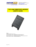
InterCEL Pty. Ltd. A.C.N. 007 077 161
33 Glenvale Crescent Mulgrave VIC. Australia 3170
Email : [email protected]
Internet : www.intercel.com.au
Ph: +61 3 9561 1666 Fax: +61 3 9561 2614
THE GSM EMBEDDED MODEM
USER’S GUIDE
History: Version 1.3
Created: 10th Oct 2001
Author: Sang Vu
Date 28th Mar 2002: Version 1.1 Modifying the 44-pin connector pinouts
Date 11th Jun 2002: Version 1.2 Modifying the power supply voltage
Date 25th Jun 2002: Version 1.3 Add details to all signals, remove the development board
Confidential
Page 1
25/06/2002
InterCEL Pty. Ltd. A.C.N. 007 077 161
33 Glenvale Crescent Mulgrave VIC. Australia 3170
Email : [email protected]
Internet : www.intercel.com.au
Ph: +61 3 9561 1666 Fax: +61 3 9561 2614
Contents
1
Introduction
3
1.1
1.2
1.3
1.4
Scope of this manual
Electrical characteristics
Mechanical characteristics
Features
1.4.1
Telephony
1.4.2
Short Message Service
1.4.3
Data
1.4.4
GPRS packet data features
1.4.5
GSM Supplementary Service
1.4.6
Others
1.5 Interfaces
2
RF Safety
2.1
2.2
2.3
2.4
General
Exposure to RF energy
Efficient modem operation
RF interference
3
Standard Compliance
5
6
3.1
3.2
3.3
3.4
GSM Phase II compliance
Safety compliance
EMC compliance
FTA compliance
3.4.1
IMEI number
3.4.2
CE label
3.5 ACA compliance
4
RF specifications
7
4.1 RF architecture
4.2 RF frequency
4.3 RF performance
4.3.1
Receiver
4.3.2
Transmitter
5
Hardware Description
8
5.1 Overview
5.2 The 44 pin connector
5.3 Signal descriptions
5.3.1
Power supply
5.3.2
SPI bus
5.3.3
Keypad interface
5.3.4
Serial link
5.3.5
SIM interface
5.3.6
General-Purpose Input/ Output
5.3.7
Audio
5.3.8
Buzzer output
5.3.9
Control signals
5.3.10 Real-time clock supply
Confidential
Page 2
25/06/2002
InterCEL Pty. Ltd. A.C.N. 007 077 161
33 Glenvale Crescent Mulgrave VIC. Australia 3170
Email : [email protected]
Internet : www.intercel.com.au
Ph: +61 3 9561 1666 Fax: +61 3 9561 2614
1 Introduction
The GEM is designed to provide a quick and easy solution to systems that need to access GSM/GPRS
network/functionality. The modem is full type approved and ready to use. It employs the proven GSM
WISMO™ technology from WAVECOM.
1.1 Scope of this manual
This document describes the hardware interface and the technical specification of the GEM. For
information about controlling the modem via the AT commands, refer to the ‘ AT command manual’.
1.2 Electrical characteristics
•
•
•
•
•
•
•
•
•
•
•
Dual band GSM modem E-GSM 900/1800 or E-GSM 900/1900
Class 4: 2W for GSM 900
Class 1: 1W for GSM 1800/1900
Voice, SMS, Fax and data
Tricodec: Full Rate, Enhanced Full Rate and Half Rate
3V SIM interface
Power supply: 3.6V to 4.2V @ 2A
300mA average current consumption
9mA in idle mode
Operating temperature: -20°C to + 55°C
Storage temperature: -35°C to +85°C
1.3 Mechanical characteristics
•
•
•
•
Small size: 62mm(L) x 38mm(W) x 12mm(H)
Weight: 25g
Casing: ABS Plastic
Mounting: 3 screw holes
1.4 Features
1.4.1
•
•
•
Telephony (TCH/FS) and Emergency calls
Full Rate, Enhanced Full Rate and Half Rate
DTMF functions
1.4.2
•
•
Short Message Service
Point to Point MT and MO
SMS Cell Broadcast
1.4.3
•
•
•
•
Telephony
Data
Data circuit asynchronous, transparent and non-transparent up to 14.4kbps
Automatic fax group 3 (Class 1 and Class2)
Alternate speech and fax
MNP2, V.42bis
Confidential
Page 3
25/06/2002
InterCEL Pty. Ltd. A.C.N. 007 077 161
33 Glenvale Crescent Mulgrave VIC. Australia 3170
Email : [email protected]
Internet : www.intercel.com.au
Ph: +61 3 9561 1666 Fax: +61 3 9561 2614
1.4.4
•
•
•
GPRS class 2 / Class B (2Rx/1Tx, GSM/GPRS switchable)
Coding schemes CS1 to CS4
Compliant with SMG31bis
1.4.5
•
•
•
•
•
•
•
•
•
GSM Supplementary Service
Call Forwarding
Call Barring
Multi Party
Call Waiting and Call Hold
Calling Line Identity
Advice of Charge
USSD
Closed User Group
Explicit Call Transfer
1.4.6
•
•
•
•
•
•
•
•
GPRS packet data features
Others
ME + SIM phone book management
Fixed Dialling Number
SIM Toolkit Class 2
SIM, network and service provider locks
Real Time Clock
Alarm management
Software upgrade through Xmodem protocol
UCS2 character set management
1.5 Interfaces
•
•
•
•
Single Antenna Interface
3V only internal SIM interface
44-pin general purpose connector
Serial RS-232C link: 300bps to 115200 bps
Confidential
Page 4
25/06/2002
InterCEL Pty. Ltd. A.C.N. 007 077 161
33 Glenvale Crescent Mulgrave VIC. Australia 3170
Email : [email protected]
Internet : www.intercel.com.au
Ph: +61 3 9561 1666 Fax: +61 3 9561 2614
2
RF safety
2.1 General
The GEM is based on the GSM standard for cellular technology. It is a low power radio transmitter and
receiver. It sends and receives radio frequency energy. The GEM radio frequency and transmit power
levels are controlled by the cellular system.
2.2 Exposure to RF energy
There has been some public concern about possible health effects of using GSM modem. After all
existing researches have been reviewed and all applicable safety standards have been met, the modem
is fitted for use.
If exposure to RF energy is still the main concern, there are ways to minimize the exposure:
Positioning the antenna and limitting the duration of the calls.
2.3 Efficient modem operation
For the modem to operate at the lowest power level, use the correct antenna and place the antenna at
the position where it gets the best possible signal strength. Do not hold the antenna while the modem is
in a call.
2.4 RF interference
Most of the electronic equipments are shielded against RF energy. However, RF energy may affect
some equipment that is inadequately shielded. To use the modem near particular electronic equipment,
check with the manufacturer’s shielding specifications.
Confidential
Page 5
25/06/2002
InterCEL Pty. Ltd. A.C.N. 007 077 161
33 Glenvale Crescent Mulgrave VIC. Australia 3170
Email : [email protected]
Internet : www.intercel.com.au
Ph: +61 3 9561 1666 Fax: +61 3 9561 2614
3
Standard Compliance
The GEM modem meets the following standards
3.1 GSM Phase II compliance
•
•
•
•
EN 301 419-1, (GSM 13.01) April 2000, Version 4.1.1
EN 301 420 (GSM 13.02) December 1999, Version 4.0.1
ETS 300 607-1, (GSM 11.10-1) September 2000, Version 4.28.1
GT.01, December 2000, Version 4.7.0
3.2 Safety
•
EN 60950: 2000 (3rd edition) : Safety of information technology equipment
3.3 EMC
•
•
•
•
EN 301 489-7: 2000
EN 301 489-1: 2000
EN 50081-1: 1992
EN50082-1: 1997
3.4 FTA compliance
The GEM has received a Full-Type approval (according to normal MS requirements) in the
configuration using the internal SIM interface.
3.4.1
•
•
•
IMEI number
TAC: 500246
FAC: 66
Serial number: 000000 to 999999
3.4.2
CE label
The GEM is CE compliant, which implies that the modem is in conformity with the European
Community directives and bears the CE label CE0681
3.5 ACA compliance
The modem has been declared to be ACA compliant. It bears the A-tick mark and C-tick mark, which
enables it to be used in Australia and New Zealand
Confidential
Page 6
25/06/2002
InterCEL Pty. Ltd. A.C.N. 007 077 161
33 Glenvale Crescent Mulgrave VIC. Australia 3170
Email : [email protected]
Internet : www.intercel.com.au
Ph: +61 3 9561 1666 Fax: +61 3 9561 2614
4
RF specifications
4.1 RF architecture
The RF part is based on a specific dual band chip and includes:
•
•
•
•
•
•
2 dedicated down converters
IF demodulator
All local RF & IF VCO
PLL
Transmit loop (modulator, down mixer, phase frequency comparator)
2 power amplifiers
4.2 RF frequencies
The RF functionalities comply with the Phase II EGSM 900/GSM 1800 or GSM 1900
recommendation:
•
•
Rx (EGSM): 925 to 960MHz
Tx (EGSM): 880 to 915MHz
•
•
Rx (GSM 1800): 1805 to 1880MHz
Tx (GSM 1800): 1710 to 1785MHz
•
•
Rx (GSM 1900): 1930 to 1990MHz
Tx (GSM 1900): 1850 to 1910MHz
4.3 RF performances
4.3.1
•
•
•
•
•
•
EGSM 900 sensitivity: < -102 dBm
GSM 1800/1900 sensitivity: <-102 dBm
Selectivity @ 200 KHz: > 9 dBc
Selectivity @ 400 KHz: > 41 dBc
Dynamic range: > -43 dBm
Co-channel rejection: >= 9 dBc
4.3.2
•
•
•
•
•
•
•
•
Receiver
Transmitter
Maximum output power for EGSM 900: 33dBm ± 2dB
Maximum output power for GSM 1800/1900: 30dBm ± 2dB
Minimum output power for EGSM 900: 5dBm ± 5dB
Minimum output power for GSM 1800/1900: 0dBm ± 2dB
H2 level: < -30 dBm
H3 level: < -30 dBm
Phase error at peak power: <5° RMS
Frequency error: ± 0.1 ppm max
Confidential
Page 7
25/06/2002
InterCEL Pty. Ltd. A.C.N. 007 077 161
33 Glenvale Crescent Mulgrave VIC. Australia 3170
Email : [email protected]
Internet : www.intercel.com.au
Ph: +61 3 9561 1666 Fax: +61 3 9561 2614
5
Hardware Description
5.1 Overview
The GEM includes a Wavecom Wismo3 module, a 44-pin header, a SIM-card holder and a RF
connector.
Pin1
Pin2
Pin43
Pin44
Figure 1: Modem bottom view
SIM card
Figure 2: Modem Top view
MMCX antenna
connector
Figure 3 : Modem side view
-
Modem connector : Samtec 44-pin high density
Antenna connector: MMCX
Confidential
Page 8
25/06/2002
InterCEL Pty. Ltd. A.C.N. 007 077 161
33 Glenvale Crescent Mulgrave VIC. Australia 3170
Email : [email protected]
Internet : www.intercel.com.au
Ph: +61 3 9561 1666 Fax: +61 3 9561 2614
5.2 The 44-pin connector
This connector consists of all signals, necessary for system integration. It consists of serial RS232
signals, audio input/output, general I/O, keypad, power supply and modem control signals.
Pin number
I/O type
Description
1
2
3
4
5
6
7
8
9
10
11
12
13
14
15
16
17
18
19
20
21
22
23
24
25
26
27
28
29
30
31
32
33
34
35
36
37
38
39
40
41
42
43
44
GND
ON/OFF
GND
RESET
AUXV0
BUZZER
MIC2+
SPEAKER2+
MIC2SPEAKER2RTS
DTR
RXD
DSR
TXD
CTS
DCD
RI
BOOT
GPIO4
VCC_RTC
GPIO5
GPIO0
LED
SIM_PRES
SIM_DATA
SIM_CLK
SIM_RESET
SIM_VCC
SPI_CLK
SPI_EN
SPI_IO
Key_Row0
Key_Column0
Key_Row1
Key_Column1
Key_Row2
Key_Column2
Key_Row3
Key_Column3
Key_Row4
Key_Column4
3V6
3V6
Ground, high current
Input, modem on/off control signal
Ground, high current
Input, modem reset control signal
Analogue input signal
Buzzer output
Microphone2, positive input
Speaker2, positive output
Microphone2 negative input
Speaker2, negative output
RS232 interface, input
RS232 interface, input
RS232 interface, output
RS232 interface, output
RS232 interface, input
RS232 interface, output
RS232 interface, output
RS232 interface, output
Input control signal
General Purpose input/Output 4
Supply voltage to Real-Time clock
General Purpose input/Output 5
General Purpose input/Output 0
Output, Working Indication
Input, SIM card detect
I/O , SIM data
Output, SIM clock
Output, SIM reset
Output, SIM card supply voltage
Output, SPI clock
Output, SPI enable
I/O, SPI data
I/O, Keypad Row 0
I/O, keypad Column 0
I/O, Keypad Row 1
I/O, keypad Column 1
I/O, Keypad Row 2
I/O, keypad Column 2
I/O, Keypad Row 3
I/O, keypad Column 3
I/O, Keypad Row 4
I/O, keypad Column 4
Supply voltage
Supply voltage
Pin1
Confidential
Page 9
Pin2
25/06/2002
InterCEL Pty. Ltd. A.C.N. 007 077 161
33 Glenvale Crescent Mulgrave VIC. Australia 3170
Email : [email protected]
Internet : www.intercel.com.au
Ph: +61 3 9561 1666 Fax: +61 3 9561 2614
5.3 Signal description
5.3.1
Power supply:
Pin1/Pin3 = Supply Ground.
Pin43/Pin44 = Supply input voltage
Power supply design is an important factor. In communication mode, the GSM modem transmits in
burst sequences (577µs burst every 4.615ms), therefore the power supply must be able to deliver high
current peaks in short period of time. During these peaks, the ripple voltage Vripp must be less than
50mVpp (for ripple frequency < 200KHz) or 2mVpp (for ripple frequeny > 200KHz) and the Drop
Voltage Vdrop must be less than 100mVpp.
Vsupply
Vdrop
Vripp
t=577µs
T=4.615ms
Supply voltage = 3.6V Minimum, 3V8 nominal, 4.2V absolute maximum.
Supply current = 2 amperes.
Current consumption in OFF mode: Nominal= 50µA, Maximum = 100µA
Current consumption in communication mode (assuming a 50Ω RF load):
-
During Tx burst: Norminal = 1.7A peak, Maximum = 2A peak
During Rx burst: Norminal = 75mA peak, Maximum = 80mA peak
Average in communication: Norminal 300mA, Maximum = 400mA
Average in idle: Norminal 3mA, Maximum = 6.5mA
5.3.2
SPI bus
Pin 30 = SPI_CLK
Pin 31 = SPI_EN
Pin 32 = SPI_IO
The SPI bus complies with the SPI bus standard. The maximum speed is 3.25Mb/s.
NOTE: The SPI bus is not yet implemented for AT command type of application.
5.3.3
Keypad interface
Pin 33 = Key row0
Pin 35 = Key row1
Pin 37 = Key row2
Pin 39 = Key row3
Pin 41 = Key row4
Pin 34 = Key column0
Pin 36 = Key column1
Pin 38 = Key column2
Pin 40 = Key column3
Pin 42 = Key column4
The modem provides scanning, debouncing functions. The key is reported using AT+CMER
command.
Confidential
Page 10
25/06/2002
InterCEL Pty. Ltd. A.C.N. 007 077 161
33 Glenvale Crescent Mulgrave VIC. Australia 3170
Email : [email protected]
Internet : www.intercel.com.au
Ph: +61 3 9561 1666 Fax: +61 3 9561 2614
5.3.4
Serial link
The 8 wire serial link complies with the V.24 protocol but not with the V.28 (electrical interface) due
to 3V logic.
Pin number
I/O
Description
Pin 11 (RTS)
Pin 12 (DTR)
Pin 13 (RXD)
Pin 14 (DSR)
Pin 15 (TXD)
Pin 16 (CTS)
Pin 17 (DCD)
Pin 18 (RI)
In
In
Out
Out
In
Out
Out
Out
Ready to Send
Data Terminal Ready
Receive Data
Data Set Ready
Transmit Data
Clear To Send
Data Carrier Detect
Ring Indicator
5.3.5
SIM interface
The modem has already implemented a 3V SIM card on-board. These SIM signals are given to enable
an external 3V-SIM card if required. A 5V SIM can also be implemented using an external SIM driver.
Note that if an external SIM card is implemented, only one SIM card can be inserted at any one time.
Pin Number
I/O
Description
Pin 25 (SIM_PRES)
Pin 26 (SIM_DATA)
Pin 27 (SIM_CLK)
Pin 28 (SIM_RESET)
Pin29 (SIM_VCC)
In
In/Out
Out
Out
Out
SIM card detect
Bidirectional SIM data
SIM clock
SIM reset
SIM power supply
For SIM_PRES signal: when not used, tie to Vcc. When used, a low to high transition means that the
SIM card is inserted. A high to low transition means that the SIM card is removed.
5.3.6
General purpose input / output
The modem provides 3 digital input/output signals and 1 analogue input signal. The digital I/O signals
associated with the AT+WIOR/AT+WIOW command. The 10bit analogue input (0V to 2.8V)
associated with AT+ADC command (sampling rate is 90.3Ksps)
Pin 5 = AUXV0
Pin 20 = GPIO4
Pin 22 = GPIO5
Pin 23 = GPIO0
Pin 24 = LED: The LED output can be used to drive a LED indicator via a transistor. The rate of
flashing indicates different states that the modem is in.
LED on steady: Modem is on but has not register to the network.
Slow flash: Modem has registered to the network.
Rapid flash: Modem is in communication mode.
5.3.7
Audio
5.3.7.1 Microphone:
The Microphone-2 inputs are differential. They include the biasing for an electret microphone (0.5mA
and 2V). The electret microphone’s impedance has to be around 2KΩ and can be connected directly.
Pin 7 = Microphone2 +
Confidential
Pin 9 = Microphone2 –
Page 11
25/06/2002
InterCEL Pty. Ltd. A.C.N. 007 077 161
33 Glenvale Crescent Mulgrave VIC. Australia 3170
Email : [email protected]
Internet : www.intercel.com.au
Ph: +61 3 9561 1666 Fax: +61 3 9561 2614
The gain of the Microphone input can be adjusted internally, from 30dB to 51dB, using the AT+VGT
command.
AT+VGT=
Max Vin (mVrms)
0 to 31
32 to 63
64 to 95
96 to 127
128 to 159
160 to 191
192 to 223
224 to 255
Transmit gain (dB)
43.80
31.01
21.95
15.54
11.00
7.79
5.51
3.90
30
33
36
39
42
45
48
51
Recommended characteristics for the microphone:
-
Type: Electret
Impedance: 2KΩ to 3KΩ
Sensitivity: -40dB to –50dB
SNR > 50dB minimum
5.3.7.2 Speaker
The Speaker2 outputs are push-pull amplifiers and can be loaded down to 150Ω and up to 1nF. These
outputs are differential and the output power can be adjusted by 2dB steps.
Pin 8 = Speaker2 +
Pin 10 = Speaker2 –
The Speaker gain can be adjust internally using the AT+VGR command
AT+VGR=
Max Output Level
Max speaker load
0 to 15
16 to 31
32 to 47
48 to 63
64 to 79
80 to 95
96 to 111
112 to 127
128 to 143
144 to 159
160 to 175
176 to 191
192 to 207
208 to 223
224 to 239
240 to 155
1.74 Vrms
1.38 Vrms
1.099 Vrms
0.873 Vrms
0.693 Vrms
0.551 Vrms
0.437 Vrms
0.347 Vrms
0.276 Vrms
0.219 Vrms
0.174 Vrms
0.138 Vrms
0.110 Vrms
0.087 Vrms
0.069 Vrms
0.069 Vrms
150Ω
50Ω
32Ω
32Ω
32Ω
32Ω
32Ω
32Ω
32Ω
32Ω
32Ω
32Ω
32Ω
32Ω
32Ω
32Ω
Recommended characteristics for the speaker:
-
Type: 10mW, electro-magnetic
Impedance: 32Ω to 150Ω / 1nF
Sensitivity: 110dB SPL minimum (0dB=20µPa)
Confidential
Page 12
25/06/2002
InterCEL Pty. Ltd. A.C.N. 007 077 161
33 Glenvale Crescent Mulgrave VIC. Australia 3170
Email : [email protected]
Internet : www.intercel.com.au
Ph: +61 3 9561 1666 Fax: +61 3 9561 2614
5.3.8
Buzzer output
The Buzzer output is a digital one. A buzzer can be directly connected between this output and supply
voltage (3V6). The maximum peak current is 80mA and the maximum average current is 40mA. A
diode against transient peak voltage is recommended.
Pin 6 = Buzzer output
Vbatt
Buzzer
Capacitor = 0 to 100nF depending on the buzzer type.
Recommended characteristics for the buzzer:
-
Type: Electro-magnetic
Impedance: 7Ω to 32Ω
Sensitivity: 90dB SPL minimum @ 10cm
Current: 60mA to 90mA
5.3.9
Control signals
5.3.9.1 ON/-OFF
Pin 2 = ON/OFF : This input is used to switch the modem on or off. A high level signal (3V6) has to
be applied to this input for at least 1 second, to turn the modem on. The high signal can be left until
modem is switched off. To properly switch the modem off, the On/-Off signal must be pulled to low
and AT+CPOF command must be sent to the modem to deregister
Power on sequence:
Power Supply
1s minimum
ON/-OFF
Internal Reset
240ms typ
Modem state
OFF
RESET
ON
READY
Power off sequence:
Power Supply
Network dependent
ON/-OFF
AT command
Modem state
Confidential
AT+CPOF
OK response
READY
OFF
Page 13
25/06/2002
InterCEL Pty. Ltd. A.C.N. 007 077 161
33 Glenvale Crescent Mulgrave VIC. Australia 3170
Email : [email protected]
Internet : www.intercel.com.au
Ph: +61 3 9561 1666 Fax: +61 3 9561 2614
5.3.9.2 BOOT
Pin 19 = BOOT input : This input is used to download the firmware into the modem’s Flash memory.
The internal boot procedure starts when this input is low during the modem reset. This input should be
left open when not used. If used, it must be driven by an open collector/drain.
This is a back-up download procedure. The main download procedure is to use AT+WDWL command.
(Refer to download procedure using AT command manual)
µP to drive BOOT signal
Manual activated
BOOT pin
BOOT pin
µP pin
5.3.9.3 RESET
Pin 4 = RESET input: This input is used to force a cold reset by providing a low level for at least
100µS. This Reset signal has to be considered as an emergency reset only since a reset procedure is
automatically done on power up.
If used, the Reset signal has to be driven by an open collector or open drain.
5.3.10
Real time clock supply
Pin 21 = VCC_RTC: This pin is used as a back-up power supply for the internal real-time clock when
the modem is switched off. It can be left open if not used.
Requirements:
Input voltage = 2V minimum, 2.75V maximum
Input current = 10µA nominal
Confidential
Page 14
25/06/2002
InterCEL Pty. Ltd. A.C.N. 007 077 161
33 Glenvale Crescent Mulgrave VIC. Australia 3170
Email : [email protected]
Internet : www.intercel.com.au
Ph: +61 3 9561 1666 Fax: +61 3 9561 2614
6
Antenna specifications
•
Frequency band: Dual band E-GSM 900Mhz – GSM 1800MHz/GSM 1900Mhz
Rx band
Tx band
•
•
•
EGSM 900
925-960MHz
880-915Mhz
GSM 1800
1805-1880Mhz
1710-1785Mhz
GSM 1900
1930-1990MHz
1850-1910MHz
Impedance: 50Ω
VSWR Tx max 2:1 / Rx max 2:1
Typical radiated gain: 0dBi
Confidential
Page 15
25/06/2002