1
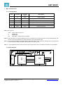
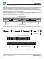
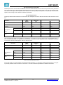
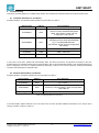
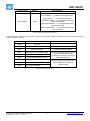
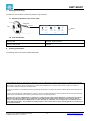
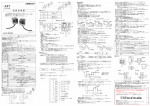
EM7180SFP 1. Main characteristics 1.1. Pin Assignment Pin# Pin Name 1 VDD I/O Type Description (note 1) PWR Supply voltage 2 SDAS OD I2C 3 SCLS OD I2C host bus SCL clock line (note 2) 4 Host_Int O Interrupt to Host MCU (note 3) 5 SA0 I I2C device address bit 0 (note 3) 6 GND PWR Ground connection host bus SDA data line (note 2) Table 1 SFP Pin Assignments Note 1: I/O Types are: PWR: I: O: OD: Power supply Connections Digital Input Digital Output Open Drain – External Pull-up is required Note 2: Note that pull-ups on I2C lines (SDAs/SCLs) are not included on the module and need to be provided externally. See Section “I2C Pull-Up Resistance” for more information on the pull-up resistor sizes. Note 3: Host_int signal should be connected to GPIO of Host MCU which can be used as an interrupt source. SA0 signal can be used to resolve unlikely I2C address alias problem on the Host I2C bus. Note 4: In most applications SA0 can be connected to ground (see Section “Host I2C Interface (Host Bus)” for more details). 1.2. Block Diagram VDD C5 0.1uF VDD SDA C6 0.1uF C7 0.1uF VDD VDDIO EEPROM 256k BMX055 9-DOF SiP SCL R1 2.4k R2 2.4k C4 0.1uF C2 4.7uF SCL SCLM SDA SDAM INT_GYRO GPIO.0 GND C3 0.01uF C1 0.47uF VDD SENTRAL U7180 VREG SCLS SCLS SDAS SDAS SA0 INT_ACC GPIO2 DRDYM GPIO4 GPIO.6 SA0 Host INT TM GND AGND GND GND Fig. 2 Sensor Fusion Platform Block Diagram Copyright 2014, EM Microelectronic-Marin SA 7180SFP-DS Version 1.1, 10-Dec-14 2 www.emmicroelectronic.com 420005-A01, 2.0