1
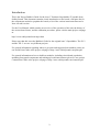
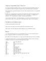
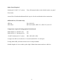
Oakley Sound Systems
5U Oakley Modular Series
TSL - Transistor Superladder
Voltage Controlled Filter
PCB Issue 3
Builder's Guide
V3.0.2
Tony Allgood
Oakley Sound Systems
CARLISLE
United Kingdom
Introduction
This is the Project Builder's Guide for the issue 3 Transistor Superladder 5U module from
Oakley Sound. This document contains a basic introduction to the board, a full parts list for
the components needed to populate the boards, a list of the various interconnections and a
'how it works' section.
For the User Manual, which contains an overview of the operation of the unit, the history of
the various board issues, and the calibration procedure, please visit the main project webpage
at:
http://www.oakleysound.com/super.htm
Please note that this is not the Builder's Guide for the original issue 3 Superladder. The SL-3
and the TSL-3 are two very different projects.
For general information regarding where to get parts and suggested part numbers please see
our useful Parts Guide at the project webpage or http://www.oakleysound.com/parts.pdf.
For general information on how to build our modules, including circuit board population,
mounting front panel components and making up board interconnects please see our generic
Construction Guide at the project webpage or http://www.oakleysound.com/construct.pdf.
2
The Transistor Superladder PCB
The issue 3 Transistor Superladder behind a natural finish Schaeffer panel. Note the optional Sock4
board which makes wiring the four sockets simple.
I have provided space for the four main control pots on the PCB. If you use the specified pots
and brackets, the PCB can be held firmly to the panel without any additional mounting
procedures. The pot spacing is 1.625” and is the same as the vertical spacing on the MOTM
modular synthesiser. The pots are; cut off frequency, resonance, resonance CV depth and filter
‘shape’.
The design requires plus and minus 15V supplies. These should be adequately regulated. The
current consumption is about 40mA for each rail. Power is routed onto the PCB by a four way
0.156” Molex type connector. You could, of course, wire up the board by soldering on wires
directly. The four pins are +15V, ground, earth/panel ground, -15V. The earth connection
allows you to connect the metal front panel to the power supply’s ground without it sharing
the modules’ ground line. More about this later.
The PCB has four mounting holes for M3 bolts, one near each corner. These are not required
if you are using the pot brackets.
3
Buffered or Unbuffered Option
The issue 3 board allows the choice to send the feedback signal through a Darlington buffer
circuit before re-entering the ladder at the bottom. The Darlington buffer or voltage follower
circuit is part of the LM13700 the TSL uses to control the feedback. However, in earlier
versions of the Superladder this was not used. TSL-3 allows the PCB to be built to either use
the buffer and drive the ladder with a voltage, or not use the buffer and to drive the ladder
directly via the OTA's current output.
The sonic differences are fairly minimal but the buffer does introduce some small amount of
non linearity or distortion to the feedback signal. This should give a slight change in the sound
when the filter is used with a large input signal and with the filter at high resonance. I'll leave it
up to you as to which one you should build but you may wish to try both and see which one
you like the best.
It is not easily possible to change modes on the fly so the board will probably built in one
mode or the other. The mode is selected by placement of a wire link and the choice of three
resistors and one capacitor. The actual details are given in the parts list.
This one has been made in the standard 'unbuffered' option. Note that pins 2 and 3 of LK1 have been
linked and R69, R70 and C27 are not fitted.
4
Transistor Superladder issue 3 Parts List
For general information regarding where to get parts and suggested part numbers please see
our useful Parts Guide at the project webpage or http://www.oakleysound.com/parts.pdf.
The components are grouped into values, the order of the component names is of no particular
consequence.
A quick note on European part descriptions. R is shorthand for ohm. K is shorthand for kiloohm. R is shorthand for ohm. So 22R is 22 ohm, 1K5 is 1,500 ohms or 1.5 kilohms. For
capacitors: 1uF = one microfarad = 1000nF = one thousand nanofarad.
To prevent loss of the small ‘.’ as the decimal point, a convention of inserting the unit in its
place is used. eg. 4R7 is a 4.7 ohm, 4K7 is a 4700 ohm resistor, 6n8 is a 6.8 nF capacitor.
The 'Buffered' and 'Unbuffered' Option
A small wire link should be fitted in LK1.
Link out pin 1, the square pad, with the middle pin, for the buffered version.
Link out pin 3, the end round pad, with the middle pin, for the unbuffered version.
Resistors
1% 0.25W metal film types are to be recommended. However, 5% ones can be used in all
places except those marked '1%' which have to be 1% or better.
R37 will be 5% since finding these in 1% is not easy and is this particular case not worthwhile.
Components marked with a * are only to be fitted if building the full 3U version. For those
building the 1U filter core version you should not fit these parts.
330R
680R 1%
1K
1K 1%
1K5
2K2
3K3
4K7 1%
10K
15K
22K
22K 1%
27K 1%
R27, R28, R24, R19
R56
R2, R6, R8, R7, R30, R5
R52
R11
R59, R41, R45
R25, R4, R3
R61, R63, R47, R49
R58, R32, R29, R15
R55, R38, R14
R35, R51, R1, R23
R46, R48, R43, R53, R60, R62, R57, R67
R64
5
33K
47K
47K 1%
68K
100K
100K 1%
120K
220K
270K
390K
750K 1%
3M3
R22
R16, R21
R54
R31, R42
R10, R33, R9, R17, R68*, R39*, R18*, R12*, R13*
R40*
R26
R44
R50
R36, R20
R66
R37
1K +3000ppm/K PTC R65
And if building the unbuffered option:
1K
R34
And if building the buffered option:
10K
47K
33K
R69
R70
R34
Capacitors
100nF multilayer ceramic
C14, C15, C16, C24, C5, C21, C22, C6, C20, C19, C4,
C3
100pF C0G 2.5mm ceramic
C13, C25
33nF, 100V polyester
1uF, 63V polyester
C7, C8, C9, C10
C23, C26, C12, C2
2u2, 63V electrolytic
220uF, 16V electrolytic
C11, C17, C18
C1
And if building the buffered option:
22uF, 35V electrolytic
C27
6
Discrete Semiconductors
BC549 NPN transistor
BC560 PNP transistor
1N4148 silicon diode
Q1, Q2, Q3, Q4, Q5, Q6, Q8, Q9
Q7
D1, D2
Integrated Circuits
TL072CN dual FET op-amp
LM13700N dual OTA
THAT300P NPN array
LM4040DIZ-10.0 10V reference
U1, U3, U4, U6, U7, U8, U9, U10
U2
U5
U11
Notes:
For U11 the LM4040CIZ-10.0 is also suitable.
For U2 the LM13600 can also be used if you are building the 'unbuffered' option. However,
the LM13600 cannot be used in place of an LM13700 if you are building the buffered version.
Trimmers (preset) resistors
10K cermet multiturn
100K cermet multiturn
100K horizontal carbon
1K horizontal carbon
22K horizontal carbon
V/OCT
TUNE
BAL, OFF2, OFF1
BPA
TWEAK
Potentiometers (Pots)
All pots Alpha 16mm PCB mounted types
47K linear
FREQUENCY, RESONANCE, RES_CV, SHAPE
Three 16mm pot brackets.
Miscellaneous
Leaded axial ferrite beads
F1, F2
MTA156 4 way header
MTA100 6-way header
PSU
PWR
– Oakley/MOTM power supply
– Synthesizers.com power supply
Molex/MTA 0.1” header 8-way
Molex/MTA 0.1” housing 8-way
I/O
I/O
– for connecting to sockets
– for connecting to sockets
7
Other Parts Required
Switchcraft 112APC 1/4” sockets
Four off mounted either on the Sock4 board or on panel
Four knobs
Around 2m of insulated multistrand hook up wire for the switch and socket connections.
Offboard Pots (3U format only)
47K Log
47K Linear
IN1, IN2, IN3
KEY SCALING, EXP CV1, EXP CV2, LIN CV
Components required if using optional Sock4 board
Molex/MTA 0.1” header 8-way
Molex/MTA 0.1” housing 8-way
I/O
I/O
112APC Switchcraft 1/4” socket
SK1, SK2, SK3, SK4
A single wire link is to be fitted to L1 on the Sock4 PCB. L2 is left open.
If using Molex KK you'll also need at least 16 crimp terminals.
Suitable lengths of wire to make up the single 100mm interconnect and two cable ties.
8
Other Notes
Q8 and Q9 are thermally locked together with cable tie.
Q8 and Q9 require special mention. These should be placed into position on the board, but
before soldering you should wrap a small cable-tie around the bodies of the devices. Tighten
the cable-tie carefully so that the flat face of each transistor is touching the other. Snip of any
excess plastic from the cable tie. This will hold them together to ensure good thermal contact.
There is no need for any thermal compound between them, but if you have some, you can add
a small bit to ensure good thermal transfer. Now solder all six leads as you would normally.
9
Connections
Power connections – MOTM and Oakley
The PSU power socket is 0.156” Molex/MTA 4-way header. Friction lock types are
recommended. This system is compatible with MOTM systems.
Power
Pin number
+15V
Module GND
Earth/PAN
-15V
1
2
3
4
Pin 1 on the I/O header has been provided to allow the ground tags of the jack sockets to be
connected to the powers supply ground without using the module’s 0V supply. Earth loops
cannot occur through patch leads this way, although screening is maintained. Of course, this
can only work if all your modules follow this principle.
Power connections – Synthesizers.com
The PWR power socket is to be fitted if you are using the module with a Synthesizers.com
system. In this case you should not fit the PSU header. The PWR header is a six way 0.1”
MTA, but with the pin that is in location 2 removed. In this way location 3 is actually pin 2 on
my schematic, location 4 is actually pin 5 and so on.
Power
Location number
Schematic Pin number
+15V
Missing Pin
+5V
Module GND
-15V
Not connected
1
2
3
4
5
6
1
2
3
4
5
+5V is not used on this module, so location 3 (pin 2) is not actually connected to anything on
the PCB.
If fitting the PWR header, you will also need to link out pins 2 and 3 of PSU. This connects
the panel ground with the module ground. Simply solder a solid wire hoop made from a
resistor lead clipping to join the middle two pads of PSU together.
10
Building the Filter Core 1U wide module using the Sock4 board
This is the simplest way of connecting all the sockets to the main board. The Sock4 board
should be populated in the way described in our construction guide found on the project
webpage. There is only one eight way header and it is to be fitted to the bottom side of the
board.
Do not forget to solder in the wire link L1. Link L2 must be left open.
You need to make up only one eight way interconnect. It should be made so that it is 100mm
long.
The prototype TSL-3 filter core module showing the detail of the board to board interconnect. Here I have
used the Molex KK 0.1” system to connect the Sock4 to the main PCB.
11
Hand wiring the sockets
If you have bought Switchcraft 112A sockets you will see that they have three connections.
One is the earth or ground tag. One is the signal tag which will be connected to the tip of the
jack plug when it is inserted. The third tag is the normalised tag, or NC (normally closed) tag.
The NC tag is internally connected to the signal tag when a jack is not connected. This
connection is automatically broken when you insert a jack.
Once fitted to the front panel the ground tags of each socket can be all connected together
with solid wire. I use 0.91mm diameter tinned copper wire for this job. It is nice and stiff, so
retains its shape. A single piece of insulated wire can then be used to connect those connected
earth tags to pin 1 of I/O. Pin 1 is the square solder pad.
All the other connections are connected to the signal or NC lugs of the sockets. The tables
below show the connections you need to make:
Pin
Pad name
Socket Connection
Lug Type
Pin 1
Pin 2
Pin 3
Pin 4
Pin 5
Pin 6
Pin 7
Pin 8
PANEL_GND
RES_CV
NC
EXP_CV1
GND
OUTPUT
GND
INPUT
Connect to all sockets
Connect to RESONANCE
No connection
Connect to FREQUENCY
Connect to FREQUENCY
Connect to OUTPUT
Connect to RESONANCE
Connect to INPUT
Earth lugs
Signal lug
Signal lug
NC lug
Signal lug
NC lug
Signal lug
3U Superladder full format
I am not going into great detail with this format as the PCB has been designed with the 1U
filter core module in mind. However, I will mention a few things that may be useful to you if
you do decide to build the larger format design.
The 3U format contains ten sockets and seven additional pots. As with the 1U module, you
need to ground the sockets' earth lugs. Do this by joining the earth lugs together first with stiff
single core wire. Since the suggested 3U layout has the sockets arranged in two groups of
four and a middle group of two, I would recommend that you use five lengths of stiff wire;
each one placed horizontally across each pair of adjacent sockets. Then, with four lengths of
thin insulated multistrand wire, connect each piece of solid wire together. Then with one more
piece of insulated wire connect one of the stiff pieces to pin 1 of the I/O header on the PCB.
Pin or pad 1 of I/O is connected to panel ground on the power sockets, ie. pin 3 on the
MTA/Molex connectors.
The pads in box labelled I/O at the bottom of the board are mainly provided for the 1U
version, but you will need to use four of these pads too. These will be pads 5 and 7 which
connect to the module ground. Also pad 6 which is the main audio output, and pad 2 which
connects to the Resonance CV input socket. Pad 1 is depicted by the square solder pad.
12
All your other connections will be made via the two 0.1" headers to the left of the board near
the pots. These are labelled AUD and CV, the former handling all the audio inputs, and the
latter the control voltage inputs.
On the headers, each odd numbered pin is the signal and all the even numbered pins are the
module ground, or 0V. The schematics show this clearly, with the AUD header shown on
page 1 on the far left, and the CV header shown in the middle of page 2. Note that the audio
input header actually has four inputs available, three which will come into the PCB via pots,
but the fourth coming direct from the fourth input socket's signal lug.
The pots have three pins. The middle pin, the wiper, will carry the signal to the appropriate
header pin on the PCB. The audio pots' wires will attach to the underside of the board at the
AUD header, and thus be soldered from the topside of the board. The CV pots' wires will
attach to the topside at the CV header and be soldered on the underside. The schematic will
show you which pad should connect to which pot's wiper lug.
The pot has two other pins, one will be connected to ground, the other to the signal lug on the
socket it controls.
With pins facing down and looking at the back of the pot, the ground connection should go to
the right hand pin. Take a wire from this pin to the pad on the PCB below the one that the
wiper connects to.
Examples:
Pin 1 of AUD goes to the wiper of the audio input LEVEL 1 pot. Pin 2 of AUD will go to the
right hand side pin of that pot.
Pin 1 of CV goes to the wiper of the KEY-SCALE pot. Pin 2 of CV will go to the right hand
side pin of that pot.
Wire up all the pots like this until all the pots are connected.
Now each pot will have one unsoldered pin left. Connect these to the appropriate socket. The
wire should go to the signal lug of the socket. That is IN 1 goes to the signal lug on the socket
labelled IN 1. Remember too, that the socket labelled IN 4 will go direct to pin 7 of the AUD
header and not need an associated pot.
There are a lot of wires here, but it should be quite neat once it is all done.
13
Circuit Description
The audio inputs are fed into the filter via a simple voltage mixer based around U1 (pins
1,2,3). Four audio inputs are given on the 3U version, but for the standard 'filter core'
modular panel we are only using one. The input levels are expected to be generally around a
maximum of 10Vp-p each. The gain of the input amplifier is such that any three inputs on the
3U version can be ran at full volume without any clipping effects being caused by the input opamp itself. However, the filter core circuitry will overdrive if the audio input level pots are set
to over 2 o’clock with a 10V p-p signal in place. This distortion is normally described as
pleasant, and works wonders on most VCO waveforms. With more complex program material
it is best probably not to run it too hard. You won’t damage the module but it will probably
sound pretty horrible. Too little input signal will produce very little waveform distortion, but
the relative noise level (mainly hiss) will be higher.
The summed output is not fed directly into the filter core like in the Oakley Multiladder, early
issues of the Superladder or most other ladder filters. In the later Transistor Superladders we
feed the output of the summing amplifier to the first VCA section. The VCA is based around
one half of a dual OTA, U2 and the other half of op-amp U1. This VCA is controlled by the
resonance pot or the relevant CV input. As the resonance, sometimes called ‘Q’ or emphasis,
is turned up, the VCA turns on letting more audio signal into the filter core. This compensates
for the drop in ‘passband’ gain normally associated with ladder filters at high resonance. So
what we are doing is actually automatically turning up the input level to the filter as the
resonance increases.
This VCA circuit is actually a ‘leaky’ one. R31 constantly bleeds audio into the filter even
when the VCA is off. Thus audio is still getting to the filter at low values of resonance. In the
old issues of the Superladder I did this Q-compensation at the output sections of the filter; in
other words, turning up the volume at the final stage of the module. Although this worked
very well, it did tend to make the filter noisier at high values of Q. The newer method is much
quieter and leads to more consistent overdrive characteristics too.
C2 and R9 pass the audio signal into the ladder filter itself. The filter is based around the
traditional ladder as designed originally by Dr. Moog in the 1960s. I have used an THAT300P
matched transistor array for the top and bottom pairs in the ladder. This minimises control
current breakthrough to a small value. Current breakthrough manifests itself as a copy of the
modulating signals on the output. Generally, this is not a good thing. The trimmer ‘BAL’
biases the base of U6, via R37, by a small amount to even out any differences within the
ladder. This minimises breakthrough still further.
Four CV inputs control the filter cut-off frequency via an exponential convertor, U9 and a pair
of NPN transistors, Q8 and 9. KEY-CV, EXP_CV1 and EXP_CV2 all provide exponential
CV responses. LIN_CV directly controls the current in the filter ladder, and as such is a sort
of linear control input. In the 1U 'Filter core' module, we will only be using the EXP_CV1
input which is roughly set to a sensitivity 0.7V/octave. All the other frequency CV inputs are
left unused. In the 3U modular set up we will be using four additional pots, mounted
externally to the board, to control the level of the KEY-CV (for keyboard scaling), both
EXP_CVs (general CV inputs) and LIN_CV inputs (another CV input).
14
The exponential convertor is temperature compensated. R65 is the positive temperature
coefficient resistor providing an approximate cancellation of the exponential converter’s
inherent temperature coefficient. The Superladder uses a +3000ppm/K 1K ‘positive temp co’
and a 27K resistor for R64 to create the necessary temperature compensated -18mV/octave
voltage input to the base of the expo converter’s input NPN transistor. It should be noted that
although the transistors are not hand matched, modern transistors do show remarkable
similarities if bought from the same manufacturer these days. It is my opinion that perfect
matching is not necessary for a filter's exponential convertor. However, to minimise
temperature drift I do recommend that the transistors are placed and held together with a
cable tie.
The V/OCT trimmer provides adjustment of the exponential scaling factor. This will allow the
VCF to be set up to track a VCO’s output if set to the standard 1V/octave. In the 1U version
of the Superladder we have little need for this trimmer as our only CV input is to be set at
approximately 0.7V/octave. The 3U version, however, has a dedicated KEY CV input socket,
and associated scaling pot, which is designed to be used with the 1V/octave keyboard CV
coming from a midi-CV convertor or analogue controller. In reality exact 1V/octave
sensitivity is not really that critical unless you use the Superladder as an oscillator.
It must be said at this point that I have deliberately restricted the maximum resonance at very
low frequencies, thus the VCF will not oscillate across the whole audio band. This has the
wonderful effect of creating a ‘punchier’ bass. Decreasing the size of C12 to 100nF will
enhance this effect even more. Although at this value the filter will not oscillate much below
1kHz.
Resonance is controlled by the ‘RESONANCE’ pot and the RES_CV input. The RES_CV
input is fed into a reversible attenuator circuit. This circuit allows the gain to be varied from -1
to +1. In other words, a CV input may be controlled in level from inverting, to off, to straight
through. Its easy to see how it works. One end of the pot is driven from a voltage follower, a
simple circuit that presents at its output a copy of what it 'sees' at its input. The other end of
the pot is connected to an inverting amplifier. This simple circuit inverts the input voltage, eg,
1V becomes -1V and -2V becomes 2V. The wiper on RES_CV pot can be moved from
inverting at one end, to non inverting at the other. In any position in between, the voltages
from each op-amp are combined in different degrees. At the centre the wiper receives signals
from both op-amps in equal proportions and the two cancel out.
Both the voltage on the Resonance pot and that from the RES_CV input are fed into voltage
followers and then onto the linear voltage to current convertor, U10a and Q7.
The current produced by U10a/Q7 actually drives two OTAs. One, we have already discussed,
increases the signal level being fed into the ladder core. The other, U2b, increases the
feedback between the top of the ladder and the inverting input of the ladder’s base transistors.
In the original Moog ladder this was achieved by a simple variable resistor. The more feedback
you apply the greater the resonance.
The trimmer, TWEAK, allows you to adjust the maximum level of resonance you require and
to compensate for any differences in transconductance of the dual OTA, U2.
15
Both halves of the dual OTA have a offset adjust trimmer. Offset manifests itself as a copy of
the resonance control voltage on the outputs of the filter. Adjusting OFF1 & OFF2 will
minimise this sufficiently as not to cause a problem.
The filter outputs are obtained by ‘looking’ at the differential voltage across the relevant filter
capacitors in the ladder. So that both four and one pole outputs are available, two differential
amplifiers (called ‘diff-amps’ for short) are used.
The two diff-amps are identical, based around the classic three-op-amp implementation. They
are all DC coupled, and rely on close matching to remove any DC offset. A differential
amplifier is a device that makes larger the voltage difference between two points. In our case,
the voltage across each filter capacitor. The gain of the differential amplifiers is set so that the
overall gain of the whole filter module is around unity with the cut-off frequency at its highest
value.
The variable ‘shape’ output is obtained by mixing the four pole output with the inverted one
pole output. Rather, than build a subtractor, I inverted the one pole output by simply wiring
the diff amp in an opposite fashion to the other one. The two output signals from each diff
amp are then simply added together by the action of the ‘SHAPE’ (or VARIABLE SLOPE on
the 3U module) pot. The combined voltages are then buffered by unity gain follower circuit,
U4b (pins 5,6,7).
The BPA trimmer, ‘band pass adjust’, is provided to compensate for any variations in the gain
of each diff amp. This is set so that the band pass response is heard when the SHAPE pot is
exactly central.
Note that the variable shape output’s phase changes depending on the position of the SHAPE
pot. This is not considered a problem, but it should be noted all the same.
16
Testing, testing, 1, 2, 3...
Apply power to the unit making sure you are applying the power correctly. Check that no
device is running hot. Any sign of smoke or strange smells turn off the power immediately and
recheck the polarity of the power supply, and the direction of the ICs in their sockets and the
polarity of the electrolytic capacitors.
Assuming everything is OK so far, it is time to apply an audio input. Use a bright signal like a
sawtooth output from a VCO. The A below middle C, 220Hz, is a good note to use.
Connect your amplifier or mixing desk input to the output socket. Set the SHAPE (or
VARIABLE SLOPE on the 3U module) pot to the far right to put the filter into four pole low
pass mode. Moving the FREQUENCY control should produce the usual and distinctive filter
effect from the 4 pole low pass output. Now turn the SHAPE (or VARIABLE SLOPE) pot to
the far left, you should hear the same sort of filter sweep sound, but with a far brighter edge to
the sound. This is the one pole (or -6dB/octave) low pass mode.
Check that rotating the SHAPE (or VARIABLE SLOPE on the 3U module) pot you can get
the sound to change from the one pole to four pole sound at either extremes of the pot’s
movements. In the middle you should get a two pole band pass filter. To test the BP response,
sweep the filter frequency up and down. At the high frequencies, the output should just sizzle,
while at the lower end the bass should be very smooth.
Turning the Resonance up will accentuate the ‘electronic’ nature of the sound on all three
outputs. Check that at maximum resonance the filter output will oscillate or get very close to
it. We can actually set the point at which resonance starts with a trimmer so don't worry at this
stage if it doesn't actually oscillate. Beware, it is quite possible to get this filter to oscillate
above the range of hearing. So be careful so as not to damage your studio monitor’s tweeters.
Listening to the four pole low pass output with the sawtooth input still connected, patch a
LFO or EG output to the FREQUENCY input. The 0.7V/octave input sensitivity of the
FREQUENCY input should produce large sweeps of cut-off, so you may want to patch in a
Multimix or other attenuating module to have some control over the sweep depth.
If you wish the FREQUENCY input to conform to 1V/octave then R42 can be changed to
100K.
If all this happens, the chances are that you have a working module.
17
Final Comments
If you have any problems with the module, an excellent source of support is the Oakley Sound
Forum at Muffwiggler.com. Paul Darlow and I are on this group, as well as many other users
and builders of Oakley modules.
If you can't get your project to work, then Oakley Sound Systems are able to offer a 'get you
working' service. If you wish to take up this service please e-mail me, Tony Allgood, at my
contact e-mail address found on the website. I can service either fully populated PCBs or
whole modules. You will be charged for all postage costs, any parts used and my time at
25GBP per hour. Most faults can be found and fixed within one hour, and I normally return
modules within a week. The minimum charge is 25GBP plus return postage costs.
If you have a comment about this builder's guide, or have a found a mistake in it, then please
do let me know. But please do not contact me or Paul Darlow directly with questions about
sourcing components or general fault finding. Honestly, we would love to help but we do not
have the time to help everyone individually by e-mail.
Last but not least, can I say a big thank you to all of you who helped and inspired me. Thanks
especially to all those nice people on the Synth-diy and Analogue Heaven mailing lists and
those at Muffwiggler.com.
Tony Allgood at Oakley Sound
Cumbria, UK
© March 2012 – updated October 2014
No part of this document may be copied by whatever means without my permission.
18