1
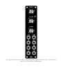
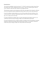
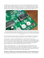
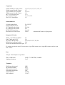
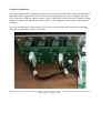
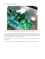
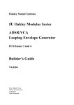
Oakley Sound Systems
5U Oakley Modular Series
VC-LFO
Low Frequency Oscillator
PCB Issue 3
Builder’s Guide
V3.0.00
Tony Allgood B.Eng PGCE
Oakley Sound Systems
CARLISLE
United Kingdom
The suggested panel layout of the issue 3 VC-LFO module. This is different to the older issue 1 VC-LFO panel in
that we lose a switch and gain an additional pot.
Introduction
This is the Project Builder's Guide for the issue 3 VC-LFO 5U module from Oakley Sound. Please
note that the issue 3 PCB is marked incorrectly as issue 2. The way to tell them apart is that true
issue 3 boards are fitted with a HFT trimmer in top right hand corner.
This document contains a basic introduction to the board, a description of the schematic, a full parts
list for the components needed to populate the boards, and a list of the various interconnections.
For the User Manual, which contains an overview of the operation of the unit, the history of the
various board issues, and all the calibration procedures, please visit the main project webpage at:
http://www.oakleysound.com/lfo.htm
For general information regarding where to get parts and suggested part numbers please see our
useful Parts Guide at the project webpage or http://www.oakleysound.com/parts.pdf.
For general information on how to build our modules, including circuit board population, mounting
front panel components and making up board interconnects please see our generic Construction
Guide at the project webpage or http://www.oakleysound.com/construct.pdf.
The issue 3 VC-LFO PCB
The issue 3 PCB mounted behind a natural finish panel. Note the use of the optional Sock8 socket board to
facilitate the wiring up of all those sockets.
I have provided space for the three main control pots on the PCB. If you use the specified 16mm
Alpha pots and matching brackets, the PCB can be held firmly to the panel without any additional
mounting procedures. The pot spacing is 1.625” and is the same as the vertical spacing on the
MOTM modular synthesiser and most of our other modules.
The design requires plus and minus 15V supplies. The power supply should be adequately
regulated. The current consumption is about 40mA for each rail. Power is routed onto the PCB by a
four way 0.156” MTA156 type connector or the special five way Synthesizers.com MTA100
header. You could, of course, wire up the board by soldering on wires directly. The four pins are
+15V, ground, earth/panel ground, -15V. The earth/panel connection allows you to connect the
metal front panel to the power supply’s ground without it sharing the modules’ ground line. More
about this later.
The PCB has four mounting holes for M3 bolts, one near each corner. These are not required if you
are using the two 16mm pot brackets.
The board size is 104mm (high) x 104mm (deep).
The board has been laid out to accept connection to our Sock8 socket board. This small board
speeds up the wiring of the eight sockets and reduces the chances of mistakes.
Circuit Description
The VC-LFO circuit consists of several sections spread over two pages; the CV summer and
exponential convertor (page 1), the VC-LFO core (page 2), sine shaper (page 1), sawtooth shaper
page 2), LED driver (page 1) and power supplies (page 2).
Looking at the bottom of page 2 of the schematic is the power supply section. This includes the
power supply inlets, PWR and PSU, and the power supply filtering components.
U1 provides a stable +5V supply for the DG403's digital input circuitry. The original VC-LFO
boards had no such supply and the DG403 was driven from +15V only. However, when Vishay
bought out Siliconix, the original manufacturer of the device, some of the specifications changed, in
particular the lower threshold voltage for the analogue switch control. This meant that the Vishay
specimens of DG403 when used in the VC-LFO did not correctly respond to sync pulses. Vishay
DG403 devices required a higher voltage than what provided by my sync input circuit and +5V gate
signals were not able to reset the LFO core reliably. By driving the logic part of the DG403 from a
5V supply this insensitivity to input levels is removed.
Two grounds are provided, one for the circuit itself, and one for the earthing of the jack sockets on
the front panel. There are eight ICs on this PCB, and each requires power, and the mass of
capacitors nearby are power supply decoupling. Both these sections of the circuit are separated from
the main circuit to avoid cluttering up the main parts of the diagram. On the PCB itself those
decoupling capacitors are actually as close the action as they can be. The closer those caps are to
their parent IC, the more effective they become. They are like little reservoirs of charge to provide
the current to the IC when it needs it. And they can usually supply it faster than the power supply
itself, if only for a very short period of time.
The VC-LFO’s pitch is determined by a variety of sources. Two CV inputs, one pot and a switch on
the front panel, and a trimmer to set initial frequency. U2a (pins 1, 2, 3) is built as a voltage
summer. It takes the voltages from the six sources and adds them together. The gain of the summer
is set by the input resistors and R7. The output of the CV summer is then fed to an inverting
amplifier of adjustable gain via the V/OCT trimmer. The V/OCT trimmer is adjusted to give a rise
of one octave in output frequency when the KEY-CV input voltage goes up by 1V. The output of
this amplifier is then fed to the exponential convertor via R47 and TC.
The exponential convertor is based around on half of U3b (pins 5, 6, 7) and the matched PNP pair
of U7. Its output is a current that is proportional to the exponent of the voltage applied at the base of
the left hand transistor of U7. The circuit gives the VC-LFO a sensitivity of roughly +18mV/octave,
so R47 and TC reduce the output of the CV summer to this level. However, it is worth noting that
TC is a temperature sensitive resistor. The resistance of TC will go up with temperature at a rate of
0.35% for every degree Celsius. This should counteract the temperature effects produced by the
semiconductor junctions in U6. To get the best temperature stability TC is mounted right on top of
U7. This way the temperature of the two devices should be the same.
It is possible to get an exponential response from a single transistor, but that has problems as Vbe,
the junction voltage, changes with ambient temperature. The ‘temp co’ resistor cannot compensate
for this change in the transistor’s operating current. So the now classic circuit with two perfectly
matched transistors and an op-amp, U7 and U3b, is used. Changes in the Vbe for one half of the
transistor pair are mirrored in the other. The op-amp then matches the current in the first transistor
with the same current in the other one. So the collector current in the first transistor will effectively
control the collector current in the second. And it is the current drawn by the second transistor that
controls the frequency of the VCO.
The output of the exponential convertor is a current. It is this current that controls the core of the
oscillator. Contrary to most people’s ideas, the core of a VCO is typically a linear CCO. That is a
current controlled oscillator. A doubling of current to the CCO will produce a doubling of output
frequency. The core of this VC-LFO creates a triangle wave from which all the other waveshapes
are created. This is different to the standard sawtooth core design used by the Oakley VCO.
A KRL +3500ppm/K positive temperature coefficient resistor bent over the top of the transistor array U7. Note
the preforming of the device's leads to make it fit snugly into place. This is a more expensive and bigger PTC
resistor than the recommended one and is probably a little over the top for a VC-LFO. The smaller +3000ppm/K
device is quite adequate. You could also use some heat conducting paste for better thermal conductivity between
the two devices.
The core itself is built from two main parts. An integrator and a schmitt trigger. The output from
each feeds into the next, and then right round again. We will start by looking at each bit in turn.
The heart of the VC-LFO core is the LM13700 IC, U8. This is a dual OTA (operational
transconductance amplifier). The OTA is different in several respects to a usual op-amp. Firstly, its
output is a current, not a voltage. Secondly, its gain is controlled by a current injected into the Iabc
pin. ‘I’ is for current, ‘abc’ stands for amplifier bias current. The bigger this current the higher the
gain of the OTA. However, the current into the Iabc pin of the 13700 must not exceed 2mA
otherwise damage will result to the OTA. R42 limits the Iabc to a safe value.
Together with op-amp U9a (pins 1, 2, 3), U8a forms the non-inverting integrator whose time
constant is controlled by the Iabc. Any negative voltage applied to pin 4 of U8, will cause the
voltage to fall at the output of the op-amp. The speed at which the voltage falls is controlled by C12
and the Iabc current. If the applied voltage to pin is positive the op-amp’s output will rise. It is the
integrator’s output that will be used as the source for the triangle output.
The DG403 is configured as four electronically controlled switches. They are arranged in pairs, so
that when one switch of the pair is closed the other is open. When a switch is closed the signal can
pass through pretty much unaffected. One channel of the DG403 (pins 5 & 6) is wired so that the
output of the integrator passes straight to the schmitt trigger. This connection can be broken when
the sync pulse is applied, but more about this later.
The schmitt trigger is a simple circuit block based around the other half of the OTA. It is configured
as an inverting schmitt trigger and its output, at pin 12 is either high at +1.8V, or low at -1.8V. If
the output of the Schmitt is initially low, it requires an input of less than -1.8V at the output of the
integrator to make it go high. Conversely, the integrator will need to produce an output of +1.8V to
make the Schmitt go low again.
To make any oscillator you normally require an output to be fed back into the input. In the VCLFO, the non inverting integrator is fed by the output of the inverting schmitt trigger. Thus, a ‘high’
at the output of the schmitt causes the integrator to rise. When the integrator’s output reaches a
certain point, the schmitt switches state and the integrator’s output falls. The schmitt trigger changes
state once again, and the process repeats itself....
C12 effectively controls the overall range of frequencies produced by the VC-LFO. You may want
to try different values for this capacitor. Lower values of C12 will give you a faster oscillator.
Indeed, the VC-LFO will make a very nice audio only VCO if you make C12 1nF.
The two back to back zener diodes, D3 and D4, strapped across the input of U8b prevent the input
voltage at pin 13 exceeding the maximum allowed by the LM13700. In ordinary operation this will
never happen, but in some cases, if your power supply comes up too slowly, the integrator output
can get too positive (or too negative) for the briefest of moments and the schmitt trigger 'latches up'.
This nasty bit of behaviour is when the input devices within the LM13700 get turned on too hard
and draw excessive current through the input pins. If latch up has occurred then only by removing
the input signal to pin 13 (with an active sync pulse) or by powering down the module can the input
be unlatched. The two diodes prevent any such latch up occurring in first place no matter what the
power supply does on power up.
A tri-colour LED is used to give the user an idea of LFO speed. It will change colour depending on
whether the integrator is charging or discharging. It is driven from two transistors, Q1 and Q2,
directly from the square wave output.
The triangle output of the module needs to be increased in level before sending out to the front
panel. The raw triangle signal is taken from the integrator’s output and passed into an inverting
amplifier, built around U9b, to increase the +/-1.8V signal to the required +/-5V output level.
The square wave output is derived from the output of the schmitt trigger. It is then fed to an non
inverting amplifier, built around U5a, to give use the standard +/-5V output.
When a pulse or gate appears at the ‘sync’ input, the pulse or gate is shaped by C3, R6 and D2 to
give a short positive spike. This controls the two channels of the DG403. Normally, as I mentioned
earlier, this part of the DG403 allows the integrator output to pass straight to the Schmitt trigger.
However, when a spike is present at pin 10 of the DG403, two things happen. Firstly, the integrator
output is cut off from the schmitt trigger by the opening of the FET switch between pins 5 and 6.
R20 will then force the schmitt trigger’s input low and the Schmitt’s output will be set low.
Secondly, the integrator capacitor will be shorted out, by the closing of the FET switch between
pins 8 and 9. This will set the integrator’s output at zero volts. When the ‘sync’ spike fades away,
the integrator will start to ramp positive due to the positive voltage from the schmitt trigger. If we
did not force the Schmitt low then the integrator would have randomly ramped either up or down.
The sawtooth and ramp shaping circuitry looks complex, but it can be broken down quite simply.
U5b acts as a dual mode circuit, it is either a buffer or an inverter. It acts on the amplified triangle
wave output. What mode it is in is determined by the switch within one of the channels of the
DG403. When the internal switch is closed, U4 acts as a inverting amplifier with gain -1. Pin 5 is
effectively tied to ground by the action of the switch. But when the switch is opened, pin 5 is
attached to the triangle wave input via R23 and R26. These two resistors form a parallel
combination of exactly 11K. U4 now acts as a unity gain buffer, ie. an amplifier with a gain of +1.
The switch in U3 is controlled by the square wave output. That means when the integrator is
discharging it is switched off and U4 is in ‘buffer’ mode. When the integrator is charging, U4 is in
inverting mode. The triangle input is then switched rapidly from being buffered and unaffected, to
being inverted. This chops the regular up and down waveform of the triangle into two sections, one
as before, the other tipped upside down. This creates two sections of ramping up, ie. a ramp
waveform but of twice the original frequency. By adding a square wave signal to this ramp signal in
the correct proportions we get another ramp waveform but at the original frequency.
U10b (pins 5, 6, 7) is a standard inverting summing circuit. It combines the square wave and twice
frequency ramp signal and inverts the sum to get a sawtooth. This is our sawtooth waveform and
this is goes through R37 to connect to the output socket. A ramp waveform is simply created by
inverting the sawtooth output with an inverting op-amp based around U10a (pins 1, 2, 3), shown on
page one.
The sine wave shaper circuit, also shown on page one of the schematics, acts upon the raw triangle
wave output of the integrator. The rounded peaks of the sine wave are created by deliberately
overdriving the inputs of a differential amplifier built around the NPN pair in U7 and recovery
amplifier U2a. The non linearities of the input stage being utilised to squash the top and bottom
peaks of the triangle wave input. The gain of the shaper is fixed partly by R57. SHP adjusts the
amount of overdrive.
R58 and R59 provide a special feedback path, called emitter degeneration, within the input circuit.
This causes the input devices to be tickled even further into overdrive at the critical peaks of the
output waveform.
The trimmer, OFF, provides compensation for any small imbalance in the NPN transistors. Any
differences in base-emitter voltages between the two transistors will make them soft clip
asymmetrically. By adding a small voltage of the opposite polarity to one of the input pins, we can
cancel the effects of the offset.
The sine wave created by this process does not give us a perfect textbook example of a sine wave.
However, the wave is very low in harmonics and has a nice rounded shape. This makes is perfect
for modulation purposes and sounds good too.
Issue 3 VC-LFO Parts List
For general information regarding where to get parts and suggested part numbers please see our
useful Parts Guide at the project webpage or http://www.oakleysound.com/parts.pdf.
The components are grouped into values, the order of the component names is of no particular
consequence.
A quick note on European part descriptions. R is shorthand for ohm. K is shorthand for kilo-ohm. R
is shorthand for ohm. So 22R is 22 ohm, 1K5 is 1,500 ohms or 1.5 kilohms. For capacitors: 1uF =
one microfarad = 1000nF = one thousand nanofarad.
To prevent loss of the small ‘.’ as the decimal point, a convention of inserting the unit in its place is
used. eg. 4R7 is a 4.7 ohm, 4K7 is a 4700 ohm resistor, 6n8 is a 6.8 nF capacitor.
Resistors
All resistors should be 0.25W 1% metal film (MF) types unless stated.
22R
390R
1K
2K
3K
3K3
4K7
5K6
10K
18K
20K
22K
30K
33K
39K
47K
51K
68K
100K
180K
220K
470K
680K
1M
R1
R45, R52
R38, R37, R36, R34, R40, R2, R3
R30
R41
R43
R57
R29, R39
R33, R42, R5, R18, R35
R53
R58, R59
R23, R27, R4, R26, R24
R21
R15, R50, R32
R46, R47, R44, R25, R28
R16
R22, R54, R49, R11, R48
R7, R55
R20, R6, R19, R14, R12
R9
R13
R10, R17, R51, R56
R8
R31
1K +3000ppm/K PTC
TC*
* This is fitted across U7 and soldered only after U7 has been placed. See picture earlier on in this
document.
Capacitors
100nF multilayer axial ceramic
150pF ceramic low-K 2.5mm
33pF ceramic low-K 2.5mm
470pF ceramic low-K 2.5mm
4n7, 63V polyester film
2u2, 63V electrolytic
22uF, 25V electrolytic
C4, C10, C6, C5, C13, C14, C7
C3
C8, C11
C9
C12
C1, C15, C16
C2
Semiconductors
1N4148 signal diode
BAT42 Schottky diode
2V7 500mW zener diode
6V2 500mW zener diode
BC550 NPN transistor
Red/Green tri-colour LED
D1, D5, D7
D6
D3, D4
D2
Q1, Q2
LED1
- Mounted off board via flying wires.
Integrated Circuits
78L05 +5V 100mA regulator
LM13700N dual OTA
TL072CN dual op-amp
DG403 dual analogue switch
THAT340 matched NPN/PNP pair
U1
U8
U10, U6, U3, U5, U2, U9
U4
U7
IC sockets can also be used. You need two 16 pin DIL sockets, one 14 pin DIL socket, and six 8 pin
DIL sockets.
Pots
All pots 16mm Alpha or equivalent.
47K or 50K linear
Alpha pot brackets
FINE, CV1-DEPTH, COARSE
2 off
Trimmers
500R 6mm horizontal
2K 6mm horizontal
50K 6mm horizontal
100K 6mm horizontal
100K multiturn
20K multiturn
SHP
HFT
STEP
OFF
TUNE
V/OCT
Miscellaneous
Leaded axial ferrite beads
L1, L2
MTA156 4 way header
MTA100 6-way header
PSU – Oakley/MOTM power supply
PWR – Synthesizers.com power supply
Molex/MTA 0.1” header 6-way
Molex/MTA 0.1” header 8-way
Molex/MTA 0.1” housing 6-way
Molex/MTA 0.1” housing 8-way
UPR
LWR
UPR
LWR
Molex/MTA 0.1” housing 3-way
5mm clear LED lens
LED1 – optional connecting technique for the tri-colour LED.
LED1
Switchcraft 112APC 1/4” sockets
Eight off mounted either on the Sock8 board or on panel
– for connecting to sockets
– for connecting to sockets
– for connecting to sockets
– for connecting to sockets
Two knobs
Power lead MTA to MTA connector
Additional components required if using optional Sock8 board
Molex/MTA 0.1” header 6-way
Molex/MTA 0.1” header 8-way
Molex/MTA 0.1” housing 6-way
Molex/MTA 0.1” housing 8-way
UPR
LWR
UPR
LWR
112APC Switchcraft 1/4” socket
SK1, SK2, SK3, SK4, SK5, SK6, SK7, SK8
If using Molex KK you'll also need at least 28 crimp terminals.
Suitable lengths of wire to make up the two interconnects and three cable ties.
Connections
Power connections – MOTM and Oakley
The PSU power socket is 0.156” Molex/MTA 4-way header. Friction lock types are recommended.
This system is compatible with MOTM systems.
Power
Pin number
+15V
Module GND
Earth/PAN
-15V
1
2
3
4
Pin 1 on the LWR header has been provided to allow the ground tags of the jack sockets to be
connected to the powers supply ground without using the module’s 0V supply. Earth loops cannot
occur through patch leads this way, although screening is maintained. Of course, this can only work
if all your modules follow this principle.
Power connections – Synthesizers.com
The PWR power socket is to be fitted if you are using the module with a Synthesizers.com system.
In this case you should not fit the PSU header. The PWR header is a six way 0.1” MTA, but with
the pin that is in location 2 removed. In this way location 3 is actually pin 2 on my schematic,
location 4 is actually pin 5 and so on.
Power
Location number
Schematic Pin number
+15V
Missing Pin
+5V
Module GND
-15V
Not connected
1
2
3
4
5
6
1
2
3
4
5
+5V is not used on this module, so location 3 (pin 2) is not actually connected to anything on the
PCB.
If fitting the PWR header, you will also need to link out pins 2 and 3 of PSU. This connects the
panel ground with the module ground. Simply solder a solid wire hoop made from a resistor lead
clipping to join the middle two pads of PSU together.
Using the Sock8 board
This is the simplest way of connecting all the sockets to the main board. The Sock8 board should be
populated in the way described in our construction guide found on the project webpage. There are
only two headers, UPR (for upper) which is six way, and LWR (for lower) which is eight way. Both
headers are fitted to the bottom side of the board. L1, the optional wire link, on the Sock8 board is
not fitted.
You need to make up two interconnects. The six way one should be made so that it is 90mm long.
The eight way should be made to be 140mm.
Both board interconnects made up and cable tied into place for neatness. This is the cheaper but perfectly decent
Molex KK 0.1” header system.
Wiring the sockets manually
If you have bought Switchcraft 112A sockets you will see that they have three connections. One is
the earth or ground tag. One is the signal tag which will be connected to the tip of the jack plug
when it is inserted. The third tag is the normalised tag, or NC (normally closed) tag. The NC tag is
internally connected to the signal tag when a jack is not connected. This connection is automatically
broken when you insert a jack.
Once fitted to the front panel the ground tags of each socket can be all connected together with solid
wire. I use 0.91mm diameter tinned copper wire for this job. It is nice and stiff, so retains its shape.
A single piece of insulated wire can then be used to connect those connected earth tags to pin 1 of
LWR. Pin 1 is the square solder pad.
The NC lugs of CV, 1V/OCT and SYNC IN sockets should be connected to module GND. This can
be found on pins 2, 3, and 5 of the UPR header.
All the other connections are connected to the signal lugs of the sockets. The tables below show the
connections you need to make:
UPR
Pin
Pad name
Socket Connection
Lug Type
Pin 1
Pin 2
Pin 3
Pin 4
Pin 5
Pin 6
SYNC-IN
module ground
module ground
KEY_CV input
module ground
CV1-IN
Connect to SYNC IN
Connect to SYNC IN
Connect to 1V/OCT
Connect to 1V/OCT
Connect to CV
Connect to CV
Signal lug
NC lug
NC lug
Signal lug
NC lug
Signal lug
Pin
Pad name
Socket Connection
Lug Type
Pin 1
Pin 2
Pin 3
Pin 4
Pin 5
Pin 6
Pin 7
Pin 8
Panel ground
RAMP-R
SAW-R
SQR-R
Not connected
SIN-R
Not connected
TRI-R
Connects to all sockets
Connect to RAMP
Connect to SAW
Connect to SQR
Ground lugs
Signal lug
Signal lug
Signal lug
Connect to SIN
Signal lug
Connect to TRI
Signal lug
LWR
Connecting the Tri-colour LED
Using a three way Molex KK housing to connect the tri-colour LED to the circuit board. The LED is held onto the
panel with a clear Cliplite lens, or equivalent, available from various places.
You may be able to wire the LED directly to the circuit board if yours has long enough leads. Most
of the ones I have seen have shorter legs than ordinary 5mm LEDs so I have to use flying wires to
connect the LED to the board. Tri-colour LEDs have three legs and each one should go to the solder
pad directly beneath it when it is mounted into the panel.
You can either solder your three wires to the LED's legs or use a MTA or Molex connector to make
the connection.
I normally wire my coloured LEDs so that they go red when the square wave output is positive.
Final Comments
If you have any problems with the module, an excellent source of support is the Oakley Sound
Forum at Muffwiggler.com. Paul Darlow and I are on this group, as well as many other users and
builders of Oakley modules.
If you can't get your project to work, then Oakley Sound Systems are able to offer a 'get you
working' service. If you wish to take up this service please e-mail me, Tony Allgood, at my contact
e-mail address found on the website. I can service either fully populated PCBs or whole modules.
You will be charged for all postage costs, any parts used and my time at 25GBP per hour. Most
faults can be found and fixed within one hour, and I normally return modules within a week. The
minimum charge is 25GBP plus return postage costs.
If you have a comment about this builder's guide, or have a found a mistake in it, then please do let
me know. But please do not contact me or Paul Darlow directly with questions about sourcing
components or general fault finding. Honestly, we would love to help but we do not have the time
to help everyone individually by e-mail.
Last but not least, can I say a big thank you to all of you who helped and inspired me. Thanks
especially to all those nice people on the Synth-diy, Oakley-Synths and Analogue Heaven mailing
lists and those at Muffwiggler.com.
Tony Allgood at Oakley Sound
Cumbria, UK
© December 2010
No part of this document may be copied by whatever means without my permission.