1
IEEE 802.15.4 PROTOCOL IMPLEMENTATION AND MEASUREMENT OF
CURRENT CONSUMPTION
by
Rajan Rai
A thesis submitted to the faculty of
The University of North Carolina at Charlotte
in partial fulfillment of the requirements
for the degree of Master of Science in the
Department of Electrical and Computer Engineering
Charlotte
2006
Approved by:
_____________________________
Dr. James M. Conrad
_____________________________
Dr. Ivan L. Howitt
_____________________________
Dr. Yogendra P. Kakad
ii
© 2006
Rajan Rai
ALL RIGHTS RESERVED
iii
ABSTRACT
RAJAN RAI. IEEE 802.15.4 Protocol Implementation and Measurement of Current
Consumption. (Under the direction of DR. JAMES M CONRAD).
This implementation is an effort towards preparing a test setup for future
enhancement and research in the area of IEEE 802.15.4 protocol. This thesis implements
a small subset of the IEEE 802.15.4 protocol to achieve a point to point communication.
The implemented protocol uses 802.15.4 MAC compliant data and acknowledgment
packets.
In the next few years, it is expected that Low Rate Wireless Personal Area Networks
(LR-WPAN) will be used in a wide variety of embedded applications, including home
automation, industrial sensing and control, environmental monitoring and sensing. In
these applications, numerous embedded devices running on batteries are distributed in an
area communicating via wireless radios. This thesis work presents a method which can be
used for current consumption of wireless data transfer embedded systems. Current
consumption is measured while doing one data packet transmission. Measurements are
compared with existing work. IEEE 802.15.4 protocol implementation is done using C
language. Code implementation is done in such a manner so that it can be ported to any
platform with minimal changes. It can also be modified to suit any special experimental
setup requirements.
iv
ACKNOWLEDGEMENTS
I would like to thank my graduate adviser Dr. James M Conrad for his
extraordinary support and understanding in guiding me through this thesis successfully. I
would also like to thank Dr. Ivan L. Howitt and Dr. Yogendra P. Kakad for providing
valuable support.
I would like to express my special thanks to Murari Raghvan for providing me
valuable help to accomplish my thesis. I also want to thank my fellow students Assad
Habib Ansari, George Sandler and Joseph Lee Johnson for providing me valuable
guidance.
v
TABLE OF CONTENTS
LIST OF FIGURES ........................................................................................................... iv
LIST OF TABLES............................................................................................................. vi
CHAPTER 1: INTRODUCTION ....................................................................................... 1
1.1 Motivation................................................................................................................. 2
1.2 Current Work ............................................................................................................ 3
1.3 Organization of Thesis.............................................................................................. 4
CHAPTER 2: INTRODUCTION TO IEEE 802.15.4 ........................................................ 8
2.1 Overview of 802.15.4 ............................................................................................... 8
2.1.1 Components of the IEEE 802.15.4 WPAN........................................................ 9
2.1.2 Network Topologies........................................................................................... 9
2.1.3 Architecture...................................................................................................... 10
2.1.3.1 PHY Specification .................................................................................... 11
2.1.3.2 MAC Sublayer Specification .................................................................... 16
2.1.4 Data Transfer Model ........................................................................................ 21
2.1.4.1 Data Transfer to a Coordinator ................................................................. 21
2.1.4.2 Data Transfer from a Coordinator............................................................. 23
2.1.4.3 Peer-to-Peer Data Transfers...................................................................... 25
CHAPTER 3: HARDWARE DESCRIPTION ................................................................. 26
3.1 Choice of Components............................................................................................ 26
3.2 Description of Hardware......................................................................................... 26
3.2.1 Overview of Chipcon ....................................................................................... 26
3.2.1.1 4-wire Serial Configuration and Data Interface........................................ 28
vi
3.2.1.2 Microcontroller Interface and Pin Description ......................................... 29
3.2.1.3 Configuration Interface............................................................................. 30
3.2.1.4 Receive Mode ........................................................................................... 31
3.2.1.5 RXFIFO Overflow .................................................................................... 32
3.2.1.6 Transmit Mode.......................................................................................... 32
3.2.1.7 General control and status pins ................................................................. 33
3.2.1.8 Radio control state machine...................................................................... 34
3.2.2 Overview of ATMEGA128L ........................................................................... 36
3.2.3 Overview of CC2420DBK Demonstration Board Kit ..................................... 37
3.2.3.1 Pin Configuration...................................................................................... 42
3.2.3.2 Programming CC2420DB Demonstration Board ..................................... 42
3.2.4 Overview of Coulomb Counter........................................................................ 43
3.2.5 Overview of STK 500 and STK 501................................................................ 48
3.3 Interfacing of Hardware.......................................................................................... 49
CHAPTER 4: SOFTWARE DEVELOPMENT ............................................................... 53
4.1 Introduction............................................................................................................. 53
4.2 AVR Software Development .................................................................................. 53
4.2.1 AVR Studio Debugger ..................................................................................... 53
4.2.2 Win AVR ......................................................................................................... 54
4.2.3 Description of Main Libraries.......................................................................... 55
4.2.3.1 Chipcon RF Communication Library ....................................................... 56
4.2.3.2 Data Transmission Protocol...................................................................... 57
4.2.3.3 One Wire Library...................................................................................... 58
vii
4.2.3.4 UART Library........................................................................................... 62
4.3 Operation of the System ......................................................................................... 62
4.3.1 Port Configuration ........................................................................................... 63
4.3.2 Data Flow......................................................................................................... 63
CHAPTER 5: POWER MEASUREMENT USING COULOMB COUNTER................ 64
5.1 Overview................................................................................................................. 64
5.2 Coulomb Counter Performance Limits................................................................... 65
5.3 Results..................................................................................................................... 67
5.3.1 Setup Used ....................................................................................................... 67
5.3.2 Readings using Coulomb Counter ................................................................... 69
5.3.3 Previous Result’s ............................................................................................. 70
5.3.4 Analysis............................................................................................................ 71
CHAPTER 6: FUTURE DEVELOPMENT ..................................................................... 72
6.1 Conclusion .............................................................................................................. 72
6.2 Potential Future Developments............................................................................... 73
6.2.1 Connect External Oscillators To Get The Minimum Current Consumption ... 73
6.2.2 Improve Current Measurement Setup using Coulomb Counter....................... 73
6.2.3 Implementation of Full Fledge IEEE 802.15.4 Protocol ................................. 73
6.2.4 Efficient Code Implementation........................................................................ 74
REFERENCES ................................................................................................................. 76
APPENDIX A: ATMEL CODE Main program of DBK_RF_UART_OneWire project79
APPENDIX B: ATMEL CODE Main program of DS2740_UART_SFD...................... 82
APPENDIX C: CURRENT MEASUREMENT USING COULOMB COUNTER........ 85
iv
LIST OF FIGURES
FIGURE 1.1 DS2740 Coulomb Counter [20]..................................................................... 5
FIGURE 1.2 ATmega 128 Pinout [13] ............................................................................... 6
FIGURE 1.3 Chipcon CC2420 Pinout – Topview [3]........................................................ 7
FIGURE 2.1 Star and peer-to-peer networks [1] .............................................................. 10
FIGURE 2.2 IEEE 802.15.4 in the ISO-OSI layered network model [1]......................... 11
FIGURE 2.3 The IEEE 802.15.4 channel structure [1] .................................................... 14
FIGURE 2.4 IEEE 802.15.4 physical layer packet structure [1] ...................................... 15
FIGURE 2.5 The general MAC frame format [1] ............................................................ 17
FIGURE 2.6 The LR-WPAN superframe structure [1] .................................................... 19
FIGURE 2.7 Communication to a coordinator in a beacon-enabled network [2] ............ 22
FIGURE 2.8 Communication to a coordinator in a nonbeacon-enabled network [2] ...... 23
FIGURE 2.9 Communication from a coordinator a beacon-enabled network [2]............ 24
FIGURE 2.10 Communication from a coordinator in a nonbeacon-enabled network [2] 25
FIGURE 3.1 Microcontroller interface example [3]......................................................... 30
FIGURE 3.2 Pin activity example during transmit [3] ..................................................... 33
FIGURE 3.3 Radio control states [3]................................................................................ 35
FIGURE 3.4 CC2420DB [4]............................................................................................. 38
FIGURE 3.5: Connector P3 with ampere meter attached [4] .......................................... 41
FIGURE 3.6 DS2740 Installed in the Host System [7] .................................................... 45
FIGURE 3.7 Interfacing of Hardware .............................................................................. 50
FIGURE 3.8 Interfacing of DS2740, Microcontroller and DBK Brd [21]....................... 51
v
FIGURE 4.1: Software download using AVR Studio 4 [4] ............................................ 54
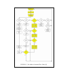
FIGURE 4.2: Library stack.............................................................................................. 56
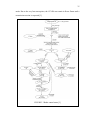
FIGURE 4.3: Net Address Command Flow Chart [10]................................................... 61
FIGURE 5.1 a) STK 500 Board........................................................................................ 67
FIGURE 5.1 b) DBK Board.............................................................................................. 68
FIGURE 5.1 c) Coulomb Counter .................................................................................... 68
FIGURE 5.1 d) Measurements Point ................................................................................ 69
FIGURE 5.1 Setup ............................................................................................................ 69
FIGURE 5.2 Single Packet Transmission for all Power Levels Mr. Neto’s measurements
[22] .............................................................................................................. 70
vi
LIST OF TABLES
TABLE 2.1 Summary of high-level characteristics. CSMA-CA: carrier sense multiple
access with collision avoidance [1].................................................................... 9
TABLE 2.2 Frequency bands and data rates [2]............................................................... 12
TABLE 2.3 IEEE 802.15.4 channel frequencies [1] ........................................................ 14
TABLE 3.1 SPI timing specification [3] .......................................................................... 29
TABLE 3.2: P3 Pinout [4] ............................................................................................... 43
TABLE 3.3: P4 Pinout [4] ............................................................................................... 44
TABLE 3.4: Memory Map [10]....................................................................................... 47
TABLE 3.5 Interface between different Devices ............................................................. 52
TABLE 4.1 Port configuration ......................................................................................... 63
TABLE 5.2 Typical Current Consumption of CC2420 and Mr. Neto’s measurements [22]
.......................................................................................................................... 70
TABLE 5.3 Low power mode signal.............................................................................. 71
TABLE C.1 Current Measurement Using Coulomb Counter for One Packet Transmission
.......................................................................................................................... 85
TABLE C.2 Current Measurement Using Coulomb Counter when Chipcon Switched off
.......................................................................................................................... 86
TABLE C.3 Average Current Measurement Per Packet Using Coulomb Counter for 10
Packet Transmission ........................................................................................ 86
vii
LIST OF ABBREVIATIONS
AES
Advanced Encryption Standard
API
Application Program Interface
ATmega 128L
AVR ATmega 128 L Microcontroller
CC2420
CHIPCON CC2420 RF Transceiver
CRC
Cyclic Redundancy Check
CSMA-CA
Carrier Sense Multiple Access with Collision Avoidance
DS2740
MAXMIM DS2740 Coulomb Counter
DSSS
Direct Sequence Spread Spectrum
EEPROM
Electrically Erasable Programmable Read Only Memory
FCS
Frame Check Sequence
FFD
Full Function Device
FIFO
First In First Out
FS
Frequency Synthesizer
GTS
Guaranteed Time Slots
I/O
Input/Output
IDE
Integrated Development Environment
ISM
Industrial, Scientific, and Medical
ITU-T
Telecommunication Standardization Sector
JTAG
Joint Test Action Group
LR-WPAN
Low-Rate Wireless Personal Area Networks
MAC
Medium Access Control Layer
MCPS
MAC Common Part Sublayer
viii
MFR
MAC Footer
MHR
MAC Header
MPDU
MAC Protocol Data Unit
m-sequence
Maximal length sequence
O-QPSK
Offset Quadrature Phase Shift Keying
OEM
Original Equipment Manufacturer
OVD
Over Drive
PA
Power Amplifier
PAN
Personal Area Network
PC
Personal Computer
PD
Power Down
PDA
Personal Digital Assistant
PHY
Physical Layer
PIO
Programmable I/O Pin
PPDU
PHY Protocol Data Unit
PSDU
PHY Service Data Unit
PWM
Pulse Width Modulation
RF
Radio Frequency
RFD
Reduced Function Device
RISC
Reduced Instruction Set Computer
RMS
Root Mean Square
RSSI
Received Signal Strength Indication
RTC
Real Time Counter
ix
RXFIFO
Receive First In First Out
SAPs
Service Access Points
SCLK
System Clock
SFD
Start of Frame Delimiter
SI
System In
SNS
Sense Resistor Input
SPI
Serial Peripheral Interface
SRAM
Static Random Access Memory
TXFIFO
Transmit First In First Out
UART
Universal Asynchronous Receiver/Transmitter
VDD
Power-Supply Input (2.7V to 5.5V)
VSS
Device Ground, Current-Sense Resistor Return
WPAN
Wireless Personal Area Network
WSN
Wireless Sensor Network
ZIF
Zero Insertion Force
CHAPTER 1: INTRODUCTION
IEEE 802.15.4 is a personal area network (PAN) wireless data communication
standard, drafted with a purpose to provide network flexibility, low cost and low power
consumption. The standard is suitable for applications in home automation requiring lowdata-rate communications in an ad hoc self-organizing network [1]. Energy efficiency is
one of the major concerns in designing and implementing wireless data communication
protocol for handheld devices and wireless sensor networks [18], IEEE 802.15.4 protocol
tries to address this issue along with many other concerns in PAN.
The main reasons why the IEEE 802.15.4 protocol was chosen for an analysis over
prevalent WPAN protocol like Bluetooth where
•
IEEE 802.15.4 standard is designed for low-data-rate, low-powerconsumption, and low-cost applications [30].
•
The complexity of Bluetooth makes it expensive and inappropriate for some
simple applications requiring low cost and low power consumption [30].
•
Bluetooth also lacks flexibility in its topologies. Besides star topologies or so
called piconets, scatternets are used in Bluetooth for supporting peer-to-peer
networks, but research work has shown that scatternets face scalability
problems [30].
•
In order to do an analysis of the IEEE 802.15.4 protocol and hardware
implementing this protocol, test benches are required. This work is a step
2
towards creating a test bench to do an analysis of the IEEE 802.15.4 protocol
which has been drafted recently.
Mr. Neto’s thesis work [22] was also a step towards providing a setup to do the study
of IEEE 802.15.4 protocol. This thesis work tries to improvise the setup and provide
software and hardware flexibility, while doing research and analysis of IEEE 802.15.4
protocol. The protocol implementation is done using C language which can be modified
as per the research requirement. By replacing oscilloscope used in Mr. Neto’s [22] setup
with Coulomb Counter it reduces cost of test bench and provides much more cost
effective setup.
Development of Evaluation board by Mr. Assad [19] provides a compact, cost
effective and flexible platform to do future studies in the field of IEEE 802.15.4 protocol.
1.1 Motivation
This work is an effort towards validating a test bench to study the energy
consumption of the wireless setup, compliant with 802.15.4, during various stages of
operation. The results obtained can be used to improve the network design to achieve
greater energy efficient devices [18]. The current prototype implementation involves a
CC2420DBK demonstration board kit, a Dallas semiconductor MAXIM DS2740 highprecision coulomb counter and a STK 500 board with ATmega128L mounted on top of
it. The CC2420DBK demonstration kit has an Atmel ATmega128L microcontroller and a
Chipcon CC2420 RF transceiver integrated on one board. The microcontroller is the logic
controller for communicating with the Chipcon radio and exchanging data with DS2740
using one-wire protocol. Code to generate Radio Frequency (RF) signals compliant with
3
IEEE 802.15.4 protocol and communicate using one-wire interface to measure current
consumption is developed in C language.
Code organization is done with the aim to give flexibility for future developers to
customize the functionality with minimal changes. Port configuration can also be easily
changed to suit different hardware configurations.
1.2 Current Work
This work is an effort towards utilizing high precision coulomb counter design by
George Sandler for a real time application [21]. Setup for this work also tries to
improvise the instruments setup used by Mr. Neto for “Development of an efficient
Energy Model for the Low-Rate - Wireless Personal Area Network (LR-WPAN)” [22].
The prototype setup is done with the aim provide the required results on a single board
with minimal overhead. Dinko Hadzic, from Oslo University has also investigated IEEE
802.15.4 for short range, low rate and low power communication technologies suitable
for use in home and industry automation. He also tried to determine the possibilities of
user interaction with the network, e.g. remote device control and monitoring using a
mobile phone or other handheld devices like Personal Digital Assistants (PDA) [23].
Hardware board designed by Mr. Assad [19] is based on setup used for taking
readings in the experiment. Mr. Murari’s [20] thesis work concentrates on testing various
hardware and software components used for taking the readings in this experiment.
Accomplishment of hardware design and test cases for verifying all components of test
bench setup establishes a foundation for future research work in the field of IEEE
802.15.4 protocol.
4
Paper titled “Performance Evaluation of the IEEE 802.15.4 MAC for Low-Rate
Low-Power Wireless Networks” [18] provides an analysis comparing the energy costs of
beacon tracking and non- tracking modes for synchronization, showing that the optimum
choice depends upon the combination of duty cycles and data rates. The MAC protocol
plays a significant role in determining the efficiency of wireless channel bandwidth [18].
This paper stresses on the importance of MAC protocol implementation on power
consumption. Results of this paper are based on NS-2 simulation.
The IEEE publication titled “Will IEEE 802.15.4 make ubiquitous networking a
reality a discussion on a potential low power, low bit rate standard” [30] discusses
potential of IEEE 802.15.4 protocol to provide low-data-rate, low-power-consumption,
and low-cost WPAN protocol.
The experiment described in paper “An experimental coin-sized radio for extremely
low-power WPAN (IEEE 802.15.4) application at 2.4 GHz” [29] is an effort towards
designing a low-power and low-rate CMOS radio composed of RF and digital circuits.
The RF design focus is to maximize linearity for a given power consumption using
linearization methods which lead an order of magnitude improvement in LNA/mixer
IIP3/power performance [29].
1.3 Organization of Thesis
The thesis is divided into six major chapters. Chapter two of the thesis report
discusses about IEEE 802.15.4 protocol. It also explains components involved in the
protocol, different types of network topologies and architecture. A functional overview of
wireless protocol along with Physical Layer (PHY) and Medium Access Control Layer
(MAC) specification is also discussed. Chapter three describes the hardware components
5
present on-board and the interfacing techniques used to integrate them. Main hardware
components used are MAXIM DS2740 coulomb counter, Atmel ATmega 128L
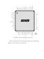
microcontroller and CHIPCON CC2420 RF transceiver. As shown in Figure 1.1, 1.2 and
1.3
FIGURE 1.1 DS2740 Coulomb Counter [20]
Chapter four describes development tools used to write, debug and compile software.
It includes a flowchart explaining the logic behind the one wire software and organization
of various libraries and data flow is covered. Chapter five presents the hardware setup
and configuration used to take the final measurement. This Chapter describes the main
limitation of coulomb counter in this setup. It also includes final readings using coulomb
counter.
6
FIGURE 1.2 ATmega 128 Pinout [13]
7
FIGURE 1.3 Chipcon CC2420 Pinout – Topview [3]
Chapter six summarizes the results and suggests possible future enhancements.
Appendix A consists of the codes of various libraries.
CHAPTER 2: INTRODUCTION TO IEEE 802.15.4
2.1 Overview of 802.15.4
There have been several attempts to network the home environment through
proprietary solutions. Recently, wireless communications has become a disruptive
technology for home networking and home automation designers. A key motivation for
use of wireless technology is the reduction in installation cost, since new wiring is not
needed. Wireless networking conveys information exchange with minimal installation
effort. This trend follows from the wider availability of cheaper and highly integrated
wireless components and the success of other wireless communication technologies such
as cellular and Wi-Fi™ IEEE 802.11b. In year 2000 two standards groups, ZigBee, a
HomeRF spinoff, and IEEE 802 Working Group 15, combined efforts to address the need
for low-power low-cost wireless networking in the residential and industrial
environments. Further more IEEE New Standards Committee (NesCom) sanctioned a
new task group to begin the development of a LR-WPAN standard, to be called 802.15.4.
The goal of this group was to provide a standard with ultra-low complexity, cost, and
power for low-data-rate wireless connectivity among inexpensive fixed, portable, and
moving devices [1]. The scope of Task Group 4 is to define the physical (PHY) and
media access control (MAC) layer specifications [1, 24]. Some of the high-level
characteristics of 802.15.4 are summarized in Table 2.1[1].
9
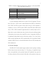
TABLE 2.1 Summary of high-level characteristics. CSMA-CA: carrier sense multiple
access with collision avoidance [1].
Property
Raw data rate
Range
Latency
Channels
Frequency band
Addressing
Channel access
Temperature
Range
868 MHz: 20kb/s; 915 MHz: 40kb/s; 2.4 GHz: 250 kb/s
10-20 m
Down to 15 ms
868/915 MHz: 11 channels
2.4 GHz: 16 channels
Two PHYs: 868 MHz/915 MHz and 2.4 GHz
Short 8-bit or 64-bit IEEE
CSMA-CA and slotted CSMA-CA
Industrial temperature range -40 to +85 C
2.1.1Components of the IEEE 802.15.4 WPAN
A system conforming to IEEE 802.15.4 consists of several components. The most
basic is the device. A device can be a reduced-function device (RFD) or a full-function
device (FFD). The FFD can operate in three modes serving as a PAN coordinator, a
coordinator, or a device. A FFD can talk to a RFDs or other FFDs, while a RFD can talk
only to a FFD. A RFD is intended for applications that are extremely simple, such as a
light switch or a passive infrared sensor; they do not have the need to send large amounts
of data and may only associate with a single FFD at a time. Consequently, the RFD can
be implemented using minimal resources and memory capacity. Two or more devices
within a personal operating space (POS) communicating on the same physical channel
constitute a WPAN. However, a network shall include at least one FFD, operating as the
PAN coordinator [2].
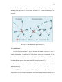
2.1.2 Network Topologies
The IEEE 802.15.4 draft standard supports multiple network topologies, including
both star and peer-to-peer networks (Figure 2.1). The topology is an application design
choice; some applications, such as personal computer (PC) peripherals, may require the
low-latency connection of the star network, while others, such as perimeter security, may
10
require the large-area coverage of peer-to-peer networking. Multiple address types,
including both physical (i.e., 64-bit IEEE) and short (i.e., 8-bit network-assigned) are
provided.
FIGURE 2.1 Star and peer-to-peer networks [1]
2.1.3 Architecture
The LR-WPAN architecture is defined in terms of a number of blocks in order to
simplify the standard. These blocks are called layers. Each layer is responsible for one
part of the standard and offers services to the higher layers. The layout of the blocks is
based on the open systems interconnection (OSI) seven-layer model [2].
The interfaces between the layers serve to define the logical links that are described
in this standard [2].
An LR-WPAN device comprises a PHY, which contains the radio RF transceiver
along with its low-level control mechanism, and a MAC sublayer that provides access to
11
the physical channel for all types of transfer. Figure 2.2 shows these blocks in a graphical
representation [2].
The upper layers, shown in Figure 2.2, consist of a network layer, which provides
network configuration, manipulation, message routing, and an application layer, which
provides the intended function of the device. An IEEE 802.2™ Type 1 logical link
control (LLC) can access the MAC sublayer through the service specific convergence
sublayer (SSCS). The LR-WPAN architecture can be implemented either as embedded
devices or as devices requiring the support of an external device such as a PC [2].
FIGURE 2.2 IEEE 802.15.4 in the ISO-OSI layered network model [1]
2.1.3.1 PHY Specification
MULTIBAND, MULTIRATE: IEEE 802.15.4 compliant device shall operate in one
or several frequency bands using the modulation and spreading formats summarized in
Table 2.2 [2].
12
TABLE 2.2 Frequency bands and data rates [2]
PHY
(MHz)
Frequency
Band
(MHz)
868/915
868-868.6
902-928
24002483.5
2450
Spreading parameters
Chip rate
(kchip/s)
300
600
2000
Data parameter
Modulation
Bitrate
BPSK
BPSK
O-QPSK
20
40
250
Symbol rate
(Ksymbol/s)
20
40
62.5
Symbols
Binary
Binary
16-ary
Orthogonal
IEEE 802.15.4 offers two PHY options that combine with the MAC to enable a
broad range of networking applications. Both PHYs are based on direct sequence spread
spectrum (DSSS) methods that result in low-cost digital IC implementation, and both
share the same basic packet structure for low-duty-cycle low-power operation. The
fundamental difference between the two PHYs is the frequency band. The 2.4 GHz PHY
specifies operation in the 2.4 GHz industrial, scientific, and medical (ISM) band, which
has nearly worldwide availability, while the 868/915 MHz PHY specifies operation in the
868 MHz band in Europe and 915 MHz ISM band in the United States [25, 26]. While
mobility between countries is not anticipated for most home networking applications, the
international availability of the 2.4 GHz band does offer advantages in terms of larger
markets and lower manufacturing costs. On the other hand, the 868 MHz and 915 MHz
bands offer an alternative to the growing congestion and other interference (microwave
ovens, etc.) associated with the 2.4 GHz band, and longer range for a given link budget
due to lower propagation losses[1].
A second distinguishing PHY characteristic of interest to network and application
designers is transmission rate. The 2.4 GHz PHY provides a transmission rate of 250
kb/s, while the 868/915 MHz PHY offers rates of 20 kb/s and 40 kb/s for its two bands,
respectively. The higher rate in the 2.4 GHz PHY is attributed largely to a higher-order
13
modulation scheme, in which each data symbol represents multiple bits. The different
transmission rates can be exploited to achieve a variety of different goals. For example,
the low rate of the 868/915 MHz PHY can be translated into better sensitivity and larger
coverage area, thus reducing the number of nodes required to cover a given physical area,
while the higher rate of the 2.4 GHz PHY can be used to attain higher throughput, lower
latency, or lower duty cycle. It is expected that each PHY will find applications for which
its strengths are best suited [1].
CHANNELIZATION: Twenty-seven frequency channels are available across the
three bands (Figure 2.3 and Table 2.3). The 868/915 MHz PHY supports a single channel
between 868.0 and 868.6 MHz, and 10 channels between 902.0 and 928.0 MHz. Due to
the regional support for these two bands, it is unlikely that a single network would ever
use all 11 channels. However, the two bands are considered close enough in frequency
that similar, if not identical, hardware can be used for both, lowering manufacturing
costs. The 2.4 GHz PHY supports 16 channels between 2.4 and 2.4835 GHz with ample
channel spacing (5 MHz) aimed at easing transmit and receive filter requirements [1].
14
FIGURE 2.3 The IEEE 802.15.4 channel structure [1]
TABLE 2.3 IEEE 802.15.4 channel frequencies [1]
Channel number
Channel center frequency
(Mhz)
K=0
K=1,2….,10
K=11,12,….,26
868.3
906+2(k-1)
2405 +5(k-11)
Since the home is likely to contain multiple types of wireless networks vying for the
same frequency bands, as well as unintentional interference from appliances, the ability
to relocate within the spectrum will be an important factor in network success.
Accordingly, the standard includes the necessary hooks to implement dynamic channel
selection, although the specific selection algorithm is left to the network layer. The MAC
layer includes a scan function that steps through the list of supported channels in search
of a beacon, while the PHY layers contain several lower-level functions, such as receiver
energy detection, link quality indication, and channel switching, which enable channel
15
assessment and frequency agility. These functions are used by the network to establish its
initial operating channel and to change channels in response to a prolonged outage [1].
To maintain a common simple interface with the MAC, both PHY layers share a
single packet structure (Figure 2.4).
FIGURE 2.4 IEEE 802.15.4 physical layer packet structure [1]
Each packet, or PHY protocol data unit (PPDU), contains a synchronization header
(preamble plus start of packet delimiter), a PHY header to indicate the packet length, and
the payload, or PHY service data unit (PSDU). The 32-bit preamble is designed for
acquisition of symbol and chip timing, and in some cases may be used for coarse
frequency adjustment. Channel equalization is not required for either PHY due to the
combination of small coverage area and relatively low chip rates. In particular, typical
root mean square (RMS) delay spread measured in residential homes is reported to be
25ns [27], which corresponds to only 2.5 percent of the shortest spread spectrum chip
period used in IEEE 802.15.4.
16
Within the PHY header, 7 bits are used to specify the length of the payload (in
bytes). This supports packets of length 0–127 bytes, although due to MAC layer
overhead, zero-length packets will not occur in practice. Typical packets sizes for home
applications such as monitoring and control of security, lighting, air conditioning, and
other appliances are expected to be on the order of 30–60 bytes, while more demanding
applications such as interactive games and computer peripherals, or multihop applications
with more address overhead, may require larger packet sizes. Adjusting for the
transmission rates in each band, the maximum packet durations are 4.25 ms for the 2.4
GHz band, 26.6 ms for the 915 MHz band, and 53.2 ms for the 868 MHz band[1].
MODULATION The 868/915 MHz PHY uses a simple DSSS approach in which
each transmitted bit is represented by a 15-chip maximal length sequence (m-sequence).
Binary data is encoded by multiplying each m-sequence by +1 or –1, and the resulting
chip sequence is modulated onto the carrier using binary phase shift keying
(BPSK).Differential data encoding is used prior to modulation to allow low-complexity
differentially coherent reception [1].
2.1.3.2 MAC Sublayer Specification
The features of the IEEE 802.15.4 MAC are association and disassociation,
acknowledged frame delivery, channel access mechanism, frame validation, guaranteed
time slot management, and beacon management. The MAC sublayer provides two
services to higher layers that can be accessed through two service access points (SAPs).
The MAC data service is accessed through the MAC common part sublayer (MCPSSAP), and the MAC management services are accessed through the MAC layer
17
management entity (MLME-SAP). These two services provide an interface between the
SSCS or another LLC and the PHY layer [1].
The MAC management service has 26 primitives. Compared to 802.15.1
(Bluetooth™), which has about 131 primitives and 32 events, the 802.15.4 MAC is of
very low complexity, making it very suitable for its intended low-end applications, albeit
at the cost of a smaller feature set than 802.15.1 (e.g., 802.15.4 does not support
synchronous voice links) [1].
THE GENERAL MAC FRAME FORMAT: The MAC frame structure is kept very
flexible to accommodate the needs of different applications and network topologies while
maintaining a simple protocol. The general format of a MAC frame is shown in Figure
2.5 [1].
FIGURE 2.5 The general MAC frame format [1]
18
The MAC frame is called the MAC protocol data unit (MPDU) and is composed of
the MAC header (MHR), MAC service data unit (MSDU), and MAC footer (MFR). The
first field of the MAC header is the frame control field. It indicates the type of MAC
frame being transmitted, specifies the format of the address field, and controls the
acknowledgment. In short, the frame controls the field, specifies how the rest of the
frame looks and what it contains [1].
The size of the address field may vary between 0 and 20 bytes. For instance, a data
frame may contain both source and destination information, while the return
acknowledgment frame does not contain any address information at all. On the other
hand, a beacon frame may only contain source address information. In addition, short 8bit device addresses or 64-bit IEEE device addresses may be used. This flexible structure
helps increase the efficiency of the protocol by keeping the packets short [1].
The payload field is variable in length; however, the complete MAC frame may not
exceed 127 bytes in length. The data contained in the payload is dependent on the frame
type. The IEEE 802.15.4 MAC has four different frame types. These are the beacon
frame, data frame, acknowledgment frame, and MAC command frame. Only the data and
beacon frames actually contain information sent by higher layers; the acknowledgment
and MAC command frames originate in the MAC and are used for MAC peer-to-peer
communication. Other fields in a MAC frame are the sequence number and frame check
sequence (FCS). The sequence number in the MAC header matches the acknowledgment
frame with the previous transmission. The transaction is considered successful only when
the acknowledgment frame contains the same sequence number as the previously
transmitted frame. The FCS helps verify the integrity of the MAC frame. The FCS in an
19
IEEE 802.15.4 MAC frame is a 16-bit International Telecommunication Union —
Telecommunication Standardization Sector (ITU-T) cyclic redundancy check (CRC)[1].
THE SUPERFRAME STRUCTURE:
Some applications may require dedicated
bandwidth to achieve low latencies. To accomplish these low latencies, the IEEE
802.15.4 LR-WPAN can operate in an optional superframe mode. In a superframe, a
dedicated network coordinator, called the PAN coordinator, transmits superframe
beacons in predetermined intervals. These intervals can be as short as 15 ms or as long as
245 s. The time between two beacons is divided into 16 equal time slots independent of
the duration of the superframe. A device can transmit at any time during a slot, but must
complete its transaction before the next superframe beacon. The channel access in the
time slots is contention-based; however, the PAN coordinator may assign time slots to a
single device requiring dedicated bandwidth or low-latency transmissions. These
assigned time slots are called guaranteed time slots (GTS) and together form a
contention-free period located immediately before the next beacon (Figure 2.6) [1].
FIGURE 2.6 The LR-WPAN superframe structure [1]
20
The size of the contention-free period may vary depending on demand by the
associated network devices; when GTS is employed, all devices must complete their
contention-based transactions before the contention-free period begins. The beginning of
the contention-free period and duration of the superframe are communicated to the
attached network devices by the PAN coordinator in its beacon [1].
OTHER MAC FEATURES:
Depending on network configuration, an LRWPAN
may use one of two channel access mechanisms. In a beacon-enabled network with
superframes, a slotted carrier sense multiple access with collision avoidance (CSMA-CA)
mechanism is used. In networks without beacons, unslotted or standard CSMA-CA is
used. This works as follows. When a device wishes to transmit in a non-beacon-enabled
network, it first checks if another device is currently transmitting on the same channel. If
so, it may back off for a random period, or indicate a transmission failure if unsuccessful
after some retries. Acknowledgment frames confirming a previous transmission do not
use the CSMA mechanism since they are sent immediately following the previous packet
[1].
In a beacon-enabled network, any device wishing to transmit during the contention
access period waits for the beginning of the next time slot and then determines if another
device is currently transmitting in the same slot. If another device is already transmitting
in the slot, the device backs off for a random number of slots or indicates a transmission
failure after some retries. In addition, in a beacon-enabled network, acknowledgment
frames do not use CSMA [1].
An important function of the MAC is confirming successful reception of a received
frame. Successful reception and validation of a data or MAC command frame is
21
confirmed with an acknowledgment. If the receiving device is unable to handle the
incoming message for any reason, the receipt is not acknowledged. The frame control
field indicates whether or not an acknowledgment is expected. The acknowledgment
frame is sent immediately after successful validation of the received frame. Beacon
frames sent by a PAN coordinator and acknowledgment frames are never acknowledged
[1].
The IEEE 802.15.4 draft standard provides for three levels of security: no security
of any type (e.g., for advertising kiosk applications); access control lists
(noncryptographic security); and symmetric key security, employing advanced
encryption standard (AES)-128. To minimize the cost for devices that do not require it,
the key distribution method (e.g., public key cryptography) is not specified in the draft
standard but may be included in the upper layers of appropriate applications [1].
2.1.4 Data Transfer Model
Three types of data transfer transactions exist. They are described in detail in the
following section. The mechanisms for each transfer type depend on whether the network
supports the transmission of beacons. A beacon-enabled network is used for supporting
low-latency devices, such as PC peripherals. If the network does not need to support such
devices, it can elect not to use the beacon for normal transfers. However, the beacon is
still required for network association [2].
2.1.4.1 Data Transfer to a Coordinator
When a device wishes to transfer data to a coordinator in a beacon-enabled network,
it first listens for the network beacon. When the beacon is found, the device synchronizes
to the superframe structure. At the appropriate point, the device transmits its data frame,
22
using slotted CSMA-CA, to the coordinator. The coordinator acknowledges the
successful reception of the data by transmitting an optional acknowledgment frame. The
transaction is now complete. This sequence is summarized in Figure 2.7 [2]
FIGURE 2.7 Communication to a coordinator in a beacon-enabled network [2]
When a device wishes to transfer data in a nonbeacon-enabled network, it simply
transmits its data frame, using unslotted CSMA-CA, to the coordinator. The coordinator
acknowledges the successful reception of the data by transmitting an optional
acknowledgment frame. The transaction is now complete. This sequence is summarized
in Figure 2.8 [2].
23
FIGURE 2.8 Communication to a coordinator in a nonbeacon-enabled network
[2]
2.1.4.2 Data Transfer from a Coordinator
This data transfer transaction is the mechanism for transferring data from a
coordinator to a device. When the coordinator wishes to transfer data to a device in a
beacon-enabled network, it indicates in the network beacon that the data message is
pending. The device periodically listens to the network beacon and, if a message is
pending, transmits a MAC command requesting the data, using slotted CSMA-CA. The
coordinator acknowledges the successful reception of the data request by transmitting an
optional acknowledgment frame. The pending data frame is then sent using slotted
CSMA-CA. The device acknowledges the successful reception of the data by transmitting
an acknowledgment frame. The transaction is now complete. Upon receiving the
acknowledgement, the message is removed from the list of pending messages in the
beacon. This sequence is summarized in Figure 2.9 [2].
FIGURE 2.9 Communication from a coordinator a beacon-enabled network [2]
When a coordinator wishes to transfer data to a device in a nonbeacon-enabled
network, it stores the data for the appropriate device to make contact and request the data.
A device may make contact by transmitting a MAC command requesting the data, using
unslotted CSMA-CA, to its coordinator at an application-defined rate. The coordinator
acknowledges the successful reception of the data request by transmitting an
acknowledgment frame. If data are pending, the coordinator transmits the data frame,
using unslotted CSMA-CA, to the device. If data are not pending, the coordinator
transmits a data frame with a zero-length payload to indicate that no data were pending.
The device acknowledges the successful reception of the data by transmitting an
acknowledgment frame. The transaction is complete. This sequence is summarized in
Figure 2.10 [2].
25
FIGURE 2.10 Communication from a coordinator in a nonbeacon-enabled
network [2]
2.1.4.3 Peer-to-Peer Data Transfers
In a peer-to-peer PAN, every device may communicate with every other device in its
radio sphere of influence. In order to do this effectively, the devices wishing to
communicate will need to either receive constantly or synchronize with each other. In the
former case, the device can simply transmit its data using unslotted CSMA-CA. In the
latter case, other measures need to be taken in order to achieve synchronization. Such
measures are beyond the scope of this standard [2].
CHAPTER 3: HARDWARE DESCRIPTION
3.1 Choice of Components
During the start of this work all the requirements to implement IEEE 802.15.4
protocol were carefully considered and the choices of hardware components were made.
Following section gives a brief description of the various hardware components used
during protocol implementation and measurement of current consumption.
3.2 Description of Hardware
3.2.1 Overview of Chipcon
The CC2420 is a true single-chip 2.4 GHz IEEE 802.15.4 compliant RF transceiver
designed for low-power and low-voltage wireless applications. Key Features of Chipcon
are as follows [3]
• True single-chip 2.4 GHz IEEE 802.15.4 compliant RF transceiver with
baseband modem and MAC support
• DSSS baseband modem with 2 MChips/s and 250 kbps effective data rate.
• Suitable for both RFD and FFD operation
• Low current consumption (RX: 19.7 mA, TX: 17.4 mA)
• Low supply voltage (2.1 – 3.6 V) with integrated voltage regulator
• Low supply voltage (1.6 – 2.0 V) with external voltage regulator
• Programmable output power
• No external RF switch / filter needed
27
• I/Q low-IF receiver
• I/Q direct upconversion transmitter
• Very few external components
• 128 (RX) + 128 (TX) byte data buffering
• Digital RSSI / LQI support
• Hardware MAC encryption (AES-128)
• Battery monitor
• QLP-48 package, 7x7 mm
• Complies with EN 300 440 and FCC CFR-47 part 15, ARIB STD-T-66
• Powerful and flexible development tools available
Figure 1.3 shows Chipcon CC2420 pinout – topview. Figure to be included
CC2420 can be configured to achieve the best performance for different applications.
Through the programmable configuration registers the following key parameters can be
programmed [3]:
• Receive / transmit mode
• RF channel selection
• RF output power
• Power-down / power-up mode
• Crystal oscillator power-up / power down
• Clear Channel Assessment mode
• Packet handling hardware support
• Encryption / Authentication modes
28
3.2.1.1 4-wire Serial Configuration and Data Interface
CC2420 is configured via a simple 4-wire SPI-compatible interface (pins SI, SO,
SCLK and CSn) where CC2420 is the slave. This interface is also used to read and write
buffered data. All address and data transfer on the SPI interface is done with most
significant bit first [3].
There are 33 16-bit configuration and status registers, 15 command strobe registers,
and two 8-bit registers to access the separate transmit and receive FIFOs. Each of the 50
registers is addressed by a 6-bit address. The RAM/Register bit (bit 7) must be cleared for
register access. The Read/Write bit (bit 6) selects a read or a write operation and makes
up the 8-bit address field together with the 6-bit address [3].
In each register read or write cycle, 24 bits are sent on the SI-line. The CSn pin (Chip
Select, active low) must be kept low during this transfer. The bit to be sent first is the
RAM/Register bit (set to 0 for register access), followed by the R/W bit (0 for write, 1 for
read). The following 6 bits are the address-bits (A5:0). A5 is the most significant bit of
the address and is sent first. The 16 data-bits are then transferred (D15:0), also MSB first.
The configuration registers can also be read by the microcontroller via the same
configuration interface. The R/W bit must be set high to initiate the data read-back.
CC2420 then returns the data from the addressed register on the 16 clock cycles
following the register address. The SO pin is used as the data output and must be
configured as an input by the microcontroller [3].
The timing for the programming is shown in Table 3.1. The clocking of the data on SI
into the CC2420 is done on the positive edge of the SCLK. When the last bit, D0, of the
29
16 data-bits has been written, the data word is loaded in the internal configuration
register.
TABLE 3.1 SPI timing specification [3]
Parameter
SCLK, clock
frequency
SCLK low
pulse
duration
SCLK high
pulse
duration
CSn setup
time
Symbol
Fsclk
Min
tcl
Max
10
Units
MHz
Conditions
25
ns
The minimum time SCLK must
be low.
tch
25
ns
The minimum time SCLK must
be high.
tsp
25
ns
CSn hold
time
tns
25
ns
SI setup time
tsd
25
ns
SI hold time
thd
25
ns
Rise time
trise
100
ns
Fall time
tfall
100
ns
The minimum time CSn must be
low before the first positive edge
of SCLK.
The minimum time CSn must be
held low after the last negative
edge of SCLK.
The minimum time data on SI
must be ready before the positive
edge of SCLK.
The minimum time data must be
held at SI, after the positive edge
of SCLK.
The maximum rise time for
SCLK and CSn
The maximum fall time for
SCLK and CSn
Multiple registers may be written without releasing CSn. The register data will be
retained during a programmed power-down mode, but not when the power-supply is
turned off (e.g. by disabling the voltage regulator using the VREG_EN pin). The registers
can be programmed in any order [3].
3.2.1.2 Microcontroller Interface and Pin Description
When used in a typical system, CC2420 will interface to a microcontroller. This
microcontroller must be able to [3]:
30
• Program CC2420 into different modes, read and write buffered data, and read back
status information via the 4-wire SPI-bus configuration interface (SI, SO, SCLK and
CSn).
• Interface to the receive and transmit FIFOs using the FIFO and FIFOP status pins.
• Interface to the CCA pin for clear channel assessment.
• Interface to the SFD pin for timing information (particularly for beaconing networks).
3.2.1.3 Configuration Interface
A CC2420 to microcontroller interface example is shown in Figure 3.1. The
microcontroller uses 4 I/O pins for the SPI configuration interface (SI, SO, SCLK and
CSn). SO should be connected to an input at the microcontroller. SI, SCLK and CSn must
be microcontroller outputs. Preferably the microcontroller should have a hardware SPI
interface [3].
FIGURE 3.1 Microcontroller interface example [3]
31
The microcontroller pins connected to SI, SO and SCLK can be shared with other
SPI-interface devices. SO is a high impedance output as long as CSn is not activated
(active low) [3].
CSn should have an external pull-up resistor or be set to a high level during power
down mode in order to prevent the input from floating. SI and SCLK should be set to a
defined level to prevent the inputs from floating [3].
3.2.1.4 Receive Mode
In receive mode, the SFD pin goes high after the start of frame delimiter (SFD) field
has been completely received. If address recognition is disabled or is successful, the SFD
pin goes low again only after the last byte of the MPDU has been received. If the
received frame fails address recognition, the SFD pin goes low immediately [3].
The FIFO pin is high when there are one or more data bytes in the RXFIFO. The first
byte to be stored in the RXFIFO is the length field of the received frame, i.e. the FIFO
pin is set high when the length field is written to the RXFIFO. The FIFO pin then remains
high until the RXFIFO is empty [3].
If a previously received frame is completely or partially inside the RXFIFO, the
FIFO pin will remain high until the RXFIFO is empty [3].
When address recognition is enabled, data should not be read out of the RXFIFO
before the address is completely received, since the frame may be automatically flushed
if it fails address recognition. This may be handled by using the FIFOP pin [3].
32
3.2.1.5 RXFIFO Overflow
The RXFIFO can only contain a maximum of 128 bytes at a given time. This may be
divided between multiple frames, as long as the total number of bytes is 128 or less. If an
overflow occurs in the RXFIFO, this is signaled to the microcontroller by setting the
FIFO pin low while the FIFOP pin is high. Data already in the RXFIFO will not be
affected by the overflow, i.e. frames already received may be read out [3].
A SFLUSHRX command strobe is required after a RXFIFO overflow to enable
reception of new data. Note that at least one byte should be read from the RXFIFO prior
to issuing the SFLUSHRX command strobe. Otherwise the FIFO will be flushed, but the
FIFOP pin will not go low before a byte is read [3].
For security enabled frames, the MAC layer must read the source address of the
received frame before it can decide which key to use to decrypt or authenticate. This data
must therefore not be overwritten even if it has been read out of the RXFIFO by the
microcontroller. If the SECCTRL0.RXFIFO_PROTECTION control bit is set, CC2420
also protects the frame header of security enabled frames until decryption has been
performed. If no MAC security is used or if it is implemented outside the CC2420, this
bit may be cleared to achieve optimal use of the RXFIFO [3].
3.2.1.6 Transmit Mode
During transmit, the FIFO and FIFOP pins are still only related to the RXFIFO. The
SFD pin is however active during transmission of a data frame, as shown in Figure 3.2.
The SFD pin goes high when the SFD field has been completely transmitted [3].
33
FIGURE 3.2 Pin activity example during transmit [3]
It goes low again when the complete MPDU (as defined by the length field) has been
transmitted or if an underflow is detected. The SFD pin behaves very similarly during
reception and transmission of a data frame. If the SFD pins of the transmitter and the
receiver are compared during the transmission of a data frame, a small delay of
approximately 2 µs can be seen because of bandwidth limitations in both the transmitter
and the receiver [3].
3.2.1.7 General control and status pins
In receive mode, the FIFOP pin can be used to interrupt the microcontroller when a
threshold has been exceeded or a complete frame has been received. This pin should then
be connected to a microcontroller interrupt pin [3].
In receive mode, the FIFO pin can be used to detect if there is data at all in the
receive FIFO. The SFD pin can be used to extract the timing information of transmitted
and received data frames. The SFD pin will go high when a start of frame delimiter has
been completely detected / transmitted. The SFD pin should preferably be connected to a
timer capture pin on the microcontroller [3].
34
3.2.1.8 Radio control state machine
The CC2420 has a built-in state machine that is used to switch between different
operation states (modes). The change of state is done either by using command strobes or
by internal events such as SFD detected in receive mode [3].
The radio control state machine states are shown in Figure 3.3
. The numbers in brackets refer to the state number readable in the FSMSTATE
status register. This functionality is primarily for test / debug purposes [3].
Before using the radio in either RX or TX mode, the voltage regulator and crystal
oscillator must be turned on and become stable [3].
The crystal oscillator is controlled by accessing the SXOSCON / SXOSCOFF
command strobes. The XOSC16M_STABLE bit in the status register returned during
address transfer indicates whether the oscillator is running and stable or not. This status
register can be polled when waiting for the oscillator to start [3].
For test purposes, the frequency synthesizer (FS) can also be manually calibrated and
started by using the STXCAL command strobe register. This will not start a transmission
before a STXON command strobe is issued. This is not shown in Figure 3.3 [3].
Enabling transmission is done by issuing a STXON or STXONCCA command
strobe. Turning off RF can be accomplished by using one of the SRFOFF or SXOSCOFF
command strobe registers [3].
After reset the CC2420 is in Power Down mode. All configuration registers can then
be programmed in order to make the chip ready to operate at the correct frequency and
35
mode. Due to the very fast start-up time, the CC2420 can remain in Power Down until a
transmission session is requested [3].
FIGURE 3.3 Radio control states [3]
36
As also described in the 4-wire Serial Configuration and Data Interface Section in
3.2.1.1, the crystal oscillator must be running in order to have access to the RAM and
FIFOs [3].
3.2.2 Overview of ATMEGA128L
The ATmega128 is a low-power CMOS 8-bit microcontroller based on the AVR
enhanced RISC architecture. By executing powerful instructions in a single clock cycle,
the ATmega128 achieves throughputs approaching 1 MIPS per MHz allowing the system
designer to optimize power consumption versus processing speed [13]. Pin configuration
of ATmega128 is shown in Figure 1.2.
This controller has 128 KB of Flash program memory, 4 KB of SRAM data memory
and 4 KB of non-volatile EEPROM data memory. The controller is interfaced to the
CC2420 via its built-in SPI interface as well as some general I/O pins [13]. Main features
of ATmega 128L which makes it suitable for implementing IEEE 802.15.4 protocol are
as follows:
•
External RAM:
The lower 4 Kbytes of the external RAM is overlaid by the
ATmega128L internal register and RAM. CC2420DB includes this memory because
it can be used for debugging purposes, to buffer and store data if desired. The 32 kB
RAM size is neither a requirement nor necessary for a low cost a FFD or RFD [13].
•
Flash Memory Requirements:
The flash requirement for a FFD device with the
Chipcon MAC will be approximate 20 kBytes and 10 - 16 kBytes for a RFD.
Additional flash size must be available for the application [4].
37
Important:
The memory requirement will be dependent on compiler, optimization
level, hardware platform and feature used in the stack [4].
•
SPI Interface:
ATmega128L has master/slave SPI serial interface which simplifies
communication between Chipcon radio and microcontroller refer Section 3.2.1.1.
•
Programmable Serial USARTs:
For displaying messages like received data due to
wireless transmission and readings taken from Coulomb Counter USART of
ATmega128L can easily be configured.
3.2.3 Overview of CC2420DBK Demonstration Board Kit
The CC2420 is a single-chip IEEE 802.15.4 compliant and ZigBee™ ready RF
transceiver. It provides a highly integrated, flexible low-cost solution for applications
using the world wide unlicensed 2.4 GHz frequency band. The CC2420DBK
demonstration board kit is a complement to the development kit (DK) as the hardware is
representative of an actual application, and it is well suited as a prototyping platform for
application code [4].
The CC2420DBK Demonstration Board Kit includes two CC2420DB Demonstration
Boards. These boards contain a CC2420 with necessary support components, an Atmel
ATmega128L AVR microcontroller, 32 KBytes external RAM, a PCB antenna, as well
as a joystick, buttons and LED's that can be used to implement a visual user application
interface. The demonstration board is also furnished with connectors where all of the
internal signals on the PCB are available [4].
38
FIGURE 3.4 CC2420DB [4]
The CC2420DB serves as a prototype platform for CC2420 software development
with an ATmega128L microcontroller. The CC2420DB provides an RS-232 connection,
39
buttons, a joystick, four LED’s, voltage regulator, temperature sensor, a potentiometer
and connectors. The connectors make it easy to interface to test equipment such as a logic
analyzer, and possible extension boards [4].
Important features of CC2420DBK board are as follows
•
Power supply section:
The power supply section contains two voltage
regulators: a 3.3 V regulator for use by the microcontroller and the I/O pins
of the CC2420. The internal regulator of CC2420 is used to generate the 1.8
voltage supply applied for powering of the CC2420 core. A diode prevents
permanent damage if a wrong polarity is applied to the board. There are two
power connectors; a 2.5mm DC jack-type connector allows us to connect an
unregulated battery eliminator easily (the positive supply is on the center
pin), and a connector for a 9V battery on the bottoms side of the PCB. It is
also possible to use 4 AA or AAA alkaline cells to power the CC2420DB if a
suitable battery pack is used [4].
•
RS-232 interface: A serial port is included on the CC2420DB. This port is
used when software is programmed into the AVR MCU using the bootloader,
and is also used by several of the example programs. The port includes
support for RTS/CTS-type hardware flow control (handshaking) [4].
•
Microcontroller and user interface: The microcontroller used is an AVR
ATmega128L from Atmel. This controller has 128 KB of Flash program
memory, 4 KB of SRAM data memory and 4 KB of non-volatile EEPROM
data memory. The controller is interfaced to the CC2420 via its built-in SPI
interface as well as some general I/O pins. The MCU is also connected to
40
four LED’s, a joystick and an extra button for user interface purposes. The
different examples use these peripherals differently. An analog temperature
sensor, a potentiometer and 64K of external RAM are also included. An ISP
and a JTAG ICE connector are provided for programming the AVR without
using the serial port. In this case an Atmel AVR JTAG or ISP programmer
should be connected to their respective connectors. All of the I/O pins are
connected to footprints for 2 x 10 pin-row connectors. These connectors are
compatible with Agilent logic analyzer probes, and can be used either for
testing or for prototyping. For instance, it is possible to add a daughter board
with additional circuitry using these connectors [4].
•
External RAM: The lower 4 Kbytes of the external RAM is overlaid by the
ATmega128L internal register and RAM. CC2420DB includes this memory
because it can be used for debugging purposes, to buffer and store data if
desired. The 32 kB RAM size is neither a requirement nor necessary for a
low cost a Full Functional Device (FFD) or Reduced Functional Device
(RFD). Please refer to the ATmega128L data sheet for more details [4].
•
Flash Memory Requirements: The flash requirement for a FFD device with
the Chipcon MAC will be approximate 20 kBytes and 10 - 16 kBytes for a
RFD. Additional flash size must be available for the application.
Important:
The memory requirement will be dependent on compiler,
optimization level, hardware platform and feature used in the stack [4].
•
CC2420DB Low Power Mode support: To apply a low power mode with
CC2420DB for application development, it will be necessary to apply an
41
additional clock source together with the 8 MHz crystal. The ATmega128L
provides the Timer/Counter oscillator pins (TOSC1 and TOSC2), and these
pins are available on the CC2420DB connector P3. The oscillator is
optimized for use with a 32.768 kHz crystal. This clock source can be
connected the following ways [4].
1. A crystal can be connected directly between the pins.
2. An external clock source can be applied to the TOSC1. Atmel does not
recommend this method.
The 32.768 kHz crystal will clock the timer 0 and then the overflow or compare
match timer interrupt is applied to wake up ATmega128 from power save mode.
•
CC2420DB Current Measurement and Consumption: It is fully possible to
measure the actual current consumption with CC2420DB. To measure the
current, jumper J1 must be removed and an ampere meter connected in series.
The current measurement is performed for the current total draw of the
CC2420DB [4].
FIGURE 3.5: Connector P3 with ampere meter attached [4]
42
To help minimize the current consumption of the CC2420DB for a specific IEEE
802.15.4 devices the default jumper J3 can be moved to enable software control of the
RS-232 driver. The external RAM will always draw 2mA in any power down mode since
its power supply cannot be disabled. Hence, if the external RAM (U3) is removed the
current consumption will decrease with 2mA. The jumper J2 is controlling the power for
the potentiometer (RT1) and temperature sensor (U2), which will also contribute to the
total current consumption in any power down mode [4].
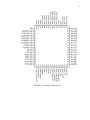
3.2.3.1 Pin Configuration
Table 3.2 and 3.3 shows the pinout available for various signals. Most important pin
for the purpose of current measurement is the Start of Frame Delimiter (SFD) signal
which is located at Pin number 19 on Port 4. SFD pin which goes high when start of
frame delimiter is detected and becomes low once packet is transmitted; it behaves in a
similar manner for received data also.
3.2.3.2 Programming CC2420DB Demonstration Board
Software can be programmed into the AVR microcontroller either using an external
programmer such as the AVR ISP programmer, AVR JTAG ICE or using the serial port
to communicate with the bootloader that is programmed into the MCU when the
CC2420DB is shipped from the factory. If the bootloader is overwritten when using an
external programmer, the AVR must be re-programmed with the bootloader before it is
possible to program the AVR via the serial port again. Note that due to the 8 MHz crystal
used with the Atmel controller, some higher Baud rates cannot be supported for
communication between the PC and the CC2420DB using the serial port. For further
43
reference please refer to the table in the Atmel ATmega 128 data sheet that lists the Baud
rate error for different crystal frequencies and Baud rates.
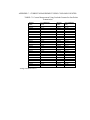
TABLE 3.2: P3 Pinout [4]
Pin number
1.
2.
Signal name in
schematic
N.C.
3.
4.
5.
6.
7.
FORCE_ON
PE4
PE2
PE0
PG3
8.
9.
PE1
PG4
10.
11.
12.
13.
14.
PE5
PE3
PE6
RTS
PE7
15.
16.
17.
18.
19.
20.
RXD1
PB7
CTS
PB4
TXD1
GND
P3 pinout
Pin Usage
N/A
Unregulated supply voltage
(Insert R101 to connect)
RS-232 on/off
Yellow LED
Joystick centre push button
ISP MOSI / Joystick up
External 32 kHz crystal /
General purpose I/O
ISP MISO / Joystick right
External 32 kHz crystal /
General purpose I/O
Push button S2
Red LED
Joystick interrupt
RS-232 handshaking
External interrupt / General
purpose I/O
RS-232 data from PC
Green LED
RS-232 handshaking
Orange LED
RS-232 data to PC
Ground
AVR pin
N/A
05 PE3
06 PE4
04 PE2
02 PE0
18 PG3
03 PE1
19 PG4
07 PE5
N/A
08 PE6
30 PD5
09 PE7
27 PD2
17 PB7
32 PD7
14 PB4
28 PD3
N/A
3.2.4 Overview of Coulomb Counter
The measurement and analysis of current consumption of the wireless
communication is accomplished by using the coulomb counter board designed by George
Sandler [21]. The coulomb counter is based on DS2740 high-precision chip for currentflow measurements. Current is measured bidirectionally over a dynamic range of 13 bits
(DS2740UB), with the net flow accumulated in a separate 16-bit register. Through its
Dallas 1-Wire interface, the DS2740 allows the host system access to real-time current
and accumulated data. FIGURE 1.1 describes Coulomb Counter pins.
44
TABLE 3.3: P4 Pinout [4]
Pin
number
1.
2.
Signal name in
schematic
N.C.
AREF
3.
4.
RESET
SCLK
5.
6.
7.
8.
9.
10.
PF1
SO
PF2
SI
PF3
VREG_EN
11.
12.
13.
14.
15.
16.
17.
18.
PF0
FIFO
CSn
FIFOP
3.3V
RESETn
N.C.
CCA
19.
SFD
20.
GND
P4 pinout
Pin Usage
N/A
Voltage reference for A/D
Converter.
RESET
CC2420 SPI clock, AVR
ISP
Joystick left
CC2420 SPI out
Joystick
CC2420 SPI in
Temperature sensor
CC2420 voltage regulator
enable
Potentiometer
CC2420 FIFO
CC2420 SPI chip select
CC2420 FIFOP
3.3V Regulated supply
CC2420 Reset
N/A
CC2420 Clear Channel
Assessment
CC2420 Start of Frame
Delimiter
Ground
CC2420 pin
N/A
N/A
AVR
pin
N/A
62
N/A
32 (SCLK)
20
11
N/A
34 (SO)
N/A
33 (SI)
N/A
41 (VREG_EN)
60
13
59
12
58
15
N/A
30 (FIFO)
31 (CSn)
29 (FIFOP)
N/A
21 (RESETn)
N/A
28 (CCA)
61
26
10
25
N/A
16
N/A
31
27 (SFD)
29
N/A
N/A
The DS2740 – high precision coulomb counter with 65µA/1µA current consumption
in active/sleep modes respectively was initially designed for battery monitoring, but can
be used to monitor consumption of any device [10].
The schematic in Figure 3.6 illustrates a possible solution for using the DS2740 in
the host system of a cell phone or personal digital assistant. The circuit shows both the
DS2740 and host system being powered by an external battery pack. The pack could be a
single-cell Lithium or triple-cell Nickel composition. The PACK+ and PACK- terminals
represent the connection to the external battery pack. The 150 Ω resistor from PACK+ to
VDD of the DS2740 is for ESD immunity.
45
FIGURE 3.6 DS2740 Installed in the Host System [7]
The resistor helps limit current spikes into the part, and protect against over-voltage
conditions. The other passive component on the VDD line is the 0.1µF capacitor. This
capacitor helps to filter voltage spikes and keep the voltage within the specified 2.7V to
5.5V range.
In the active mode of operation, the DS2740 continually measures the current flow
into and out of the battery by measuring the voltage drop across a low-value currentsense resistor, RSNS [10]. The voltage-sense range is ±51.2mV. To extend the input
range for pulse-type load currents, the voltage signal can be filtered by adding a capacitor
between the IS1 and IS2 pins (Figure 3.6). The external capacitor and two internal 10kΩ
resistors form a low-pass filter at the input of the ADC. The input converts peak signal
amplitudes up to 75mV as long as the continuous or average signal level (post filter) does
not exceed ±51.2mV over the conversion cycle period. The ADC samples the input
46
differentially and updates the current register (CR) at the completion of each conversion
cycle. There are two versions of DS2740 available: 15- and 13- bit A/Ds. With identical
analog circuits the 15-bit version has a conversion period 4 times longer then the 13-bit
version (3.2s versus 0.875s), and hence, 4 times better resolution and dynamic range. For
15-bit (DS2740) and 13-bit (DS2740B) devices, the resolution (LSB) is 1.56µV and
6.25µV respectively. One possible drawback of higher sensitivity is prolonged
conversion which may be critical in real-time applications. The range of measuring
current depends on a sense resistor RSNS and can be adjusted widely. The value of
RSNS is calculated based on maximum consumption Imax and is equal to
RSNS=51.2mV/Imax. Current resolution is 6.25µV/RSNS and 1.56µV/RSNS for 13-bit
and 15-bit versions respectively. Thus for the 13-bit device using RSNS=20mΩ, the
current resolution is 312µA LSB and dynamic range ±2.56A. For RSNS=0.1Ω, the
current resolution and dynamic range are 62.4µA and ±512 mA respectively [10].
The current measurement offset range is –3 LSBs to +5 LSBs according to datasheet
specification [10]. The positive average offset error +1 LSB caused by sharing one sense
line with device ground through VSS and can be reduced by an average of 2 LSBs
(1.9mAh per day with a 20mΩ sense) by eliminating internal resistors of RC filter and
connecting IS1 and IS2 directly to the sense resistor. The loss of the filter will have no
impact in most applications. In pulse-load cases with current spikes larger than the
dynamic range of the A/D external filter can be used [10].
Every 1024th conversion (15 minutes in the DS2740B), the ADC measures its input
offset to facilitate offset correction. During the offset correction conversion, the ADC
does not measure the IS1 to IS2 signal. To reduce the error, the current measurement just
47
prior to the offset conversion is displayed in the Current Register and is substituted for
the dropped current measurement in the current accumulation process [10].
CURRENT ACCUMULATOR: Current measurements are internally summed at the
completion of each conversion period with the results displayed in the Accumulator
Current Register (ACR). The ACR has a range of ±204.8mVh with Current
Accumulation Register resolution 6.25µVh (Both DS2740 and DS2740B). For
RSNS=20m Ω ACR resolution is 312.5µAh and range is ±10.24Ah [10].
Read and write access is allowed to the ACR. A write forces the ADC to measure its
offset and update the offset correction factor. The current measurement and accumulation
begin with the second conversion following a write to the ACR [10].
MEMORY: The DS2740 has memory space with registers for instrumentation,
status, and control. When the MSB of a two-byte register is read, both the MSB and LSB
are latched and held for the duration of the read data command to prevent updates during
the read and ensure synchronization between the two register bytes [10].
TABLE 3.4: Memory Map [10]
ADDRESS (HEX)
00
01
02 to 07
08
09 to 0D
0E
0F
10
11
12 to FF
SPECIAL BITS:
DESCRIPTION
Reserved
Status Register
Reserved
Special Feature Register
Reserved
Current Register MSB
Current Register LSB
Accumulated Current Register MSB
Accumulated Current Register LSB
Reserved
READ/WRITE
-R
-R/W
-R
R
R/W
R/W
--
These bits can be read from status registers, they can also be
modified by performing writing operation, it results in change in the operation status of
Coulomb Counter [10].
48
SMOD: Sleep Mode Enable. Status Register bit. A value of 1 allows the DS2740
to enter sleep mode when DQ is low for 2s. The power-up default of SMOD = 0
[10].
RNAOP: Read Net Address Opcode. Status Register bit. A value of 0 in this bit
sets the opcode for the read net address command to 33h, while a 1 sets the opcode
to 39h. Addressing different opcodes help save time in multi-slave systems [10].
PIO: PIO Pin Sense and Control. Special Features Register bit. This bit is read and
write enabled. Writing a 0 to the PIO bit enables the PIO open-drain output driver,
forcing the PIO pin low. Writing a 1 to the PIO bit disables the output driver,
allowing the PIO pin to be pulled high or used as an input. Reading the PIO bit
returns the logic level forced on the PIO pin [10].
3.2.5 Overview of STK 500 and STK 501
The STK500 is a complete starter kit, programming tool and development system for
Atmel’s AVR microcontrollers. The STK500 gives AVR users the freedom to develop
and test complete AVR designs and prototypes. The STK500 supports all Programming
modes of all AVR microcontrollers in the sockets as well as ISP Programming of external
target systems. The AVR I/O ports are accessible on pin headers that can be used for
connecting the on-board LEDs and push buttons, or external signals. The extra RS-232
port can be connected to any of the I/O pins. The STK500 Programming interface is
integrated in AVR Studio. The Flash, EEPROM, and all Fuse and Lock Bit options can
be programmed individually or with the sequential automatic programming option. The
AVR clock frequency and supply voltage can also be controlled from AVR Studio [16].
49
The STK501 board is a top module designed to add ATmega103(L) and
ATmega128(L) support to the STK500 development board from Atmel Corporation.
With this board the STK500 is extended to support all current AVR devices in a single
development environment [17].
The STK501 includes connectors, jumpers and hardware allowing full utilization of
the new features of the ATmega 128L while the Zero Insertion Force (ZIF) socket allows
easy use of TQFP packages for prototyping [17].
In addition to adding support for new devices, it also adds new support for
peripherals previously not supported by the STK500. An additional RS-232 port and
external SRAM interface are among the new features. Devices with dual Universal
Asynchronous Receiver/Transmitter (UART) or XRAM interface can all take advantage
of the new resources on the STK501 board [17].
3.3 Interfacing of Hardware
Figure 3.7 shows interface between different hardware. Setup to take current
consumption readings require
1. Pair of DBK board
2. One high precision Coulomb Counter designed by George Sandler
[21].
3. One STK 500 board mounted with STK501 board.
4. ATmega 128 L plugged inside STK501 board
5. PC installed with AVR Studio
50
FIGURE 3.7 Interfacing of Hardware
51
Chapter 5 explains in detail about steps involved in setup. PC running AVR studio is
used to download program on DBK board and ATmega 128L. Coulomb Counter is
interfaced with ATmega 128L microcontrollers on STK501 mounted on STK500
development board. Power supply to DBK board given from the Coulomb Counter.
Interface between the Coulomb Counter and microcontroller and DBK board is illustrated
in the Figure 3.8
FIGURE 3.8 Interfacing of DS2740, Microcontroller and DBK Brd [21]
Table 3.5 summarizes the interface between different devices. DQ pin and GND of
Coulomb Counter are connected with port C pin 6 and GND respectively of STK500
board. DBK board is interfaced with STK500 by connecting SFD pin of DBK board i.e.
pin 19 on port 4 with port A pin 1 of STK500. SFD pin act as source of trigger which
requests the microcontroller to fetch the reading of coulomb counter Current Register.
Program is written to take the reading from Coulomb Counter when SFD pin goes low to
52
high and when it goes from high to low. Difference between these two readings will
indicate the amount of current consumption for one frame. In order to display various
messages like coulomb counter readings and transferred messages UART on DBK, used
as receiver, and UART on STK501 needs to be connected to PC. RTS and CTS pin on
CC2420DBK board need to be shorted in order to configure its UART to no hardware
control. UART output from CC2420DBK Rx side need to be connected to PC serial port
to display received messages on hyper terminal. Power supply of coulomb counter comes
from STK500 board. Battery positive pin is connected to any VTG pin on STK500 and
battery negative pin is connected to any GND pin on STK500. Power supply to the DBK
board used for transmission is supplied through the Coulomb Counter. PIO pin 2 of
coulomb counter is connected to the positive terminal of 9V socket of DBK board and
SNS pin 3 is connected to negative terminal of 9V.
TABLE 3.5 Interface between different Devices
Device A
Coulomb Counter Board
Coulomb Counter Board
CC2420DBK Tx side
STK501
CC2420DBK Tx side
CC2420DBK Rx side
CC2420DBK Rx side
Coulomb Counter Board
Coulomb Counter Board
Coulomb Counter Board
Coulomb Counter Board
Pin on
Device A
DQ Pin7
GND
Port 4 Pin 19
UART
Port 3 Pin 13
Port 3 Pin 13
UART
Bat +ve 1
Bat -ve 2
PIO Pin 2
SNS Pin 3
Device B
STK500
STK500
STK500
PC
CC2420DBK Tx side
CC2420DBK Rx side
PC
STK500
STK500
CC2420DBK Tx side
CC2420DBK Tx side
Pin on Device B
Port C Pin6
Port C GND
Port A Pin1
Serial Port
Port 3 Pin 17
Port 3 Pin 17
Serial Port
Any VTG
Any Port GND
9V supply +ve
9V supply –ve
CHAPTER 4: SOFTWARE DEVELOPMENT
4.1 Introduction
During development of this project only freeware was used. Main advantages of
using freeware are as follows
•
No Licensing fee
•
Programs can be customized as per the requirement and redistributed.
Main source of freeware was www.avrfreaks.net website.
4.2 AVR Software Development
WinAVR is used for compiling and linking the main program and various libraries.
An Integrated Development Environment, AVR Studio was used for debugging the
compiled program and to download the binary image onto the AVR Microcontroller.
4.2.1 AVR Studio Debugger
AVR Studio is an Integrated Development Environment (IDE) for writing and
debugging AVR applications in Windows 9x/Me/NT/2000/XP environments. AVR
Studio provides a project management tool, source file editor, chip simulator and Incircuit emulator interface for the powerful AVR 8-bit RISC family of microcontrollers
[14].
In addition, AVR Studio supports the STK500 development board, which allows
programming of all AVR devices, and the new JTAG on-chip emulator [14].
54
Serial cable can be used to connect the serial interface of the CC2420DB to the
serial port of a PC running AVR Studio [4]. Figure 4.1 shows connection to download
software using AVR Studio
FIGURE 4.1: Software download using AVR Studio 4 [4]
4.2.2 Win AVR
WinAVR is a suite of executable, open source software development tools for the
Atmel AVR series of RISC microprocessors hosted on the Windows platform. It includes
the GNU GCC compiler for C and C++ [28].
WinAVR is a collection of executable software development tools for the Atmel
AVR processor hosted on Windows [28].
These software development tools include:
55
•
Compilers
•
Assembler
•
Linker
•
Librarian
•
File converter
•
Other file utilities
•
C Library
•
Programmer software
•
Debugger
•
In-Circuit Emulator software
•
Editor / IDE
•
Many support utilities
During development of this project WinAVR was used for compiling and linking C
code. C code was written using “Textpad” which is a free text editor for Windows.
4.2.3 Description of Main Libraries
Source Code of this project primarily can be divided into three main libraries
•
Chipcon RF Communication Library
•
One Wire Library
•
UART Library
These libraries are described in detail in below section.
56
4.2.3.1 Chipcon RF Communication Library
The CC2420 libraries and examples include a variety of source files to ease and
support the program development. Besides the standard C libraries, the source/support
files are divided into 4 main groups: Hardware Definition Files, Hardware Abstraction
Library, Basic RF library and finally application example [4].
FIGURE 4.2: Library stack
Hardware Definition Files: The hardware definition files (include files) define the
hardware registers in the MCU and the CC2420. They also include useful macros for the
CC2420DB, and all definitions generally support the C language [4].
Hardware Abstraction Library (HAL):
To support quick and easy program
development Chipcon provides a library of macros and functions that simplify hardware
access on the CC2420. These are located in the Hardware Abstraction Library (HAL) and
implement a hardware abstraction interface for the user program. As a result the user
program can access the microcontroller peripherals, etc. via function/macro calls, without
specific knowledge about the hardware details [4].
57
Basic RF Library: The "Basic RF" library contains simple functions for packet
transmission and reception with the Chipcon CC2420 radio chip. The intention of this
library is mainly to demonstrate how the CC2420 is operated, and not to provide a
complete and full functional packet protocol. The protocol uses 802.15.4 MAC compliant
data and acknowledgment packets, however it contains only a small subset of the
802.15.4 standard [4]:
•
Association, scanning, beacons is not implemented
•
No defined coordinator/device roles (peer-to-peer, all nodes are equal)
•
Waits for the channel to become ready, but does not check CCA twice
(802.15.4 CSMA-CA)
•
Does not retransmit packets
•
Can not communicate with other networks (using a different PAN identifier)
•
Short addresses only
4.2.3.2 Data Transmission Protocol
The data transmission protocol is very simple, only using data and acknowledgement
frames [4].
Step-by-Step procedure:
1. Joystick is pressed on device 2
2. CC2420 device 2 transmits the data frame
3. CC2420 device 1 receives the data frame
4. Microcontroller (uC) device 1 gets the FIFOP interrupt from CC2420, RXFIFO is
read, frame is checked for FCS, and the green LED is blinked
58
5. CC2420 device 1 waits 12 symbol periods before automatically transmitting the
acknowledgement reply
6. CC2420 device 2 receives acknowledge frame
7. Microcontroller (uC) device 2 gets the FIFOP interrupt from the CC2420,
RXFIFO is read, and frame is verified for FCS
8. The yellow LED will blink without further reply indicating the acknowledgement.
If transmission failed (no acknowledgement) the red LED will toggle.
4.2.3.3 One Wire Library
The Dallas Semiconductor 1-Wire® bus is a simple signaling scheme that performs
two-way communications between a single master and peripheral devices over a single
connection. There are over 30 different 1-Wire devices Dallas Semiconductor currently
produces. The bus master is typically a microprocessor in the host system. Each device
has a unique factory-programmed 64-bit net address that allows it to be individually
addressed by the host system, supporting multiple connections to 1-Wire bus. The
interface can be operated with standard or overdrive timing [8].
Dallas Semiconductor’s 1-Wire communication protocol can easily be implemented
on almost any microcontroller [8]:
• Only two bidirectional PIO states are necessary: high impedance and logic low. If
a bidirectional pin is not available on the bus master, separate output and input pins can
be connected together.
• The 1-Wire timing protocol has specific timing constraints that must be followed
in order to achieve successful communication. The DS2740 can operate in two
59
communication speed modes, standard and overdrive. The speed mode is determined by
the input logic level of the OVD pin.
• The 1-Wire bus must have a pullup resistor at the bus-master end of the bus. For
short line lengths, the value of this resistor should be approximately 5kΩ. The idle state
for the 1-Wire bus is high.
The protocol for accessing the DS2740 is as follows:
1. Initialization - Reset.
2. Net Address Command.
3. Function Command followed by Transaction/Data.
1. The start of any 1-Wire transaction begins with a reset pulse from the master
device followed by a simultaneous presence detect pulses from the slave devices.
2. Once the bus master has detected the presence of one or more slaves, it can issue
one of the Net Address Commands.
Search Net Address [F0h]. This command allows the bus master to use a process of
searching to identify the 1-Wire net addresses of all slave devices on the bus. In
multidrop systems this command must be used first, then Match Net Address [10].
Match Net Address [55h]. This command allows the bus master to specifically
address one DS2740 on the 1-Wire bus. Only the addressed DS2740 responds to any
subsequent function command [10].
60
Read Net Address [33h or 39h]. This command allows the bus master to read the
DS2740’s 1-Wire net address. This command can only be used if there is a single slave
with correspondent opcode on the bus. Bit RNAOP, responsible for that opcode must be
set first in a system of two DS2740s [10].
Skip Net Address [CCh]. This command saves time when there is only one DS2740
on the bus by allowing the bus master to issue a function command without specifying
the address of the slave [10].
Resume [A5h]. This command increases data throughput in multidrop environments
where the DS2740 needs to be accessed several times. After successfully executing a
Match Net Address command or Search Net Address command, an internal flag is set in
the DS2740. When the flag is set, the DS2740 can be repeatedly accessed through the
Resume command function. Accessing another device on the bus clears the flag, thus
preventing two or more devices from simultaneously responding to the Resume
command function [10].
3. After successfully completing one of the net address commands, the bus master
can access the features of the DS2740 with any of the Function Commands.
Read Data [69h, XX]. This command reads data from the DS2740 starting at
memory address XX. The LSb of the data in address XX is available to be read
immediately after the MSb of the address has been entered [10].
Write Data [6Ch, XX]. This command writes data to the DS2740 starting at memory
address XX. The LSb of the data to be stored at address XX can be written immediately
after the MSb of address has been entered. Incomplete bytes are not written [10].
FIGURE 4.3: Net Address Command Flow Chart [10]
62
4.2.3.4 UART Library
UART library used for this project is an interrupt UART library with
receive/transmit circular buffers. It was written by Peter Fleury[12]. An interrupt is
generated when the UART has finished transmitting or receiving a byte. The interrupt
handling routines use circular buffers for buffering received and transmitted data.
The UART_RX_BUFFER_SIZE and UART_TX_BUFFER_SIZE variables
define the buffer size in bytes. Note that these variables must be a power of 2.
This library is included in the HAL layer.
4.3 Operation of the System
Section 3.3 explains in detail how to interface different devices. Once respective
firmware is downloaded on different devices (refer Section 5.1 for detailed steps for the
setup). DBK boards are used to transmit and receive data based on wireless IEEE
802.15.4 data transmission protocol. RF library application program interface (API)
configures SPI ports to communicate with Chipcon. Firmware is written to transmit one
frame every time S2 button is pressed. RF API changes the status of SFD pin from low to
high when it detects start of frame and it goes to low again at the end of frame
transmission. Status of SFD pin is used as trigger to read coulomb counter current
accumulator register. Microcontroller mounted on STK501 detects the status of SFD pin
it takes reading of coulomb counter at start and end of frame transmission. Difference
between two readings tells the actual consumption during data transmission. Readings of
coulomb counter are sent to the UART of STK501 mounted on STK500 board. These
readings can be displayed on the hype terminal session with 9600 8N1 configuration.
63
4.3.1 Port Configuration
Table 4.1 shows the pin configuration used while measuring the current
consumption. SPI is configured using the Chipcon RF library.
TABLE 4.1 Port configuration
Device
STK500
STK500
STK500
PORT
Port C
Port C
Port A
PIN
Pin 6
GND
Pin 1
Configuration
Output Mode
NA
Input mode
4.3.2 Data Flow
In this experimental setup there are two main processes which involve flow of data.
•
Data communication between ATmega 128L and Chipcon to generate RF
signals for IEEE 802.15.4 protocol based wireless communication.
•
Measurements taken from coulomb counter are sent to UART.
Data communication between ATmega 128L and Chipcon is done using SPI
interface. ATmega 128L configures various registers of Chipcon using SPI. Data to be
transferred over RF and vice versa are also sent using the same interface standard.
Section 3.2.1.1 describes SPI in detail. Data communication sent to PC through UART is
based on a simple RS-232 based data interface
CHAPTER 5: POWER MEASUREMENT USING COULOMB COUNTER
5.1 Overview
Figure 3.7 shows the interface between different hardware. A detailed procedure of
the hardware setup is listed below.
1.
Load program “DS2740_UART_SFD” (refer Appendix A for code) on
ATmega 128L mounted on STK 501.
2.
Compile DBK_RF_UART_one_wire program with appropriate option of
CHIPCON_ON ( 1 for ON and 0 for OFF) and PACKETS_TO_TRANSMIT
( 1 or 10 ). Load program “DBK_RF_UART_one_wire” on pair of DBK
board. (Refer Appendix A for code).
3.
Connect PC6 of the STK500 mounted with the STK501 with DQ of Coulomb
Counter. Pull-up resistor is connected between these pins. Refer Figure 3.6 to
interface between host which in this case is ATmega 128L and DS2740.
4.
As shown in Figure 3.7 connect supply input power to the DBK board from
the Coulomb counter. Power supply for the Coulomb counter comes from the
STK 500; connect any VTG and GND pin present on the STK 500 with pin 1
and 2 respectively.
5.
Connect header 4 Pin 19 of the DBK board set as transmitter with PA1. The
SFD pin goes high at the start of every frame transmission. While taking
measurement with Chipcon switched off connect header 3 Pin 14.
65
6.
Short the RTS and CTS pin on the STK501 board, in order to achieve this,
short Pin13 and Pin17 on header 3.
7.
Connect the UART of the DBK board set up for receiving data with PC and
start HyperTerminal session with 9600 8 N1 configuration.
8.
Short RTS and CTS pin on STK501 board and connect Rx0 with PD2 and
Tx0 with PD3. Connect the UART of the STK501 with a PC and start a hyper
terminal session with 9600 8 N1 configuration.
9.
On pressing S2 button present on the DBK board 1 or 10 frames are
transmitted and the Coulomb Counter current value is read and printed on the
UART connected to STK501. In case of Chipcon switched off current value is
displayed without transmitting any packets.
5.2 Coulomb Counter Performance Limits
There are two versions of DS2740 available: 15- and 13- bit A/Ds. With identical
analog circuits the 15-bit version has a conversion period 4 times longer then the 13-bit
version (3.2s versus 0.875s), and hence, 4 times better resolution and dynamic range. For
15-bit (DS2740) and 13-bit (DS2740B) devices, the resolution (LSB) is 1.56µV and
6.25µV respectively. One possible drawback of higher sensitivity is prolonged
conversion which may be critical in real-time applications. The range of measuring
current depends on a sense resistor RSNS and can be adjusted widely. The value of RSNS is
calculated based on maximum consumption Imax and is equal to RSNS=51.2mV/Imax.
Current resolution is 6.25µV/RSNS and 1.56µV/RSNS for 13-bit and 15-bit versions
respectively. Thus for the 13-bit device using RSNS=20mΩ, the current resolution is
66
312µA LSB and dynamic range ±2.56A. For RSNS=0.1Ω, the current resolution and
dynamic range are 62.4µA and ±512 mA respectively [21].
The current measurement offset range is –3 LSBs to +5 LSBs according to the
datasheet specification [10]. The positive average offset error +1 LSB caused by sharing
one sense line with the device ground through VSS and can be reduced by an average of
2 LSBs (1.9mAh per day with a 20mΩ sense) by eliminating internal resistors of an RC
filter and connecting IS1 and IS2 directly to the sense resistor. The loss of the filter will
have no impact in most applications.
Every 1024th conversion (15 minutes in the DS2740B), the ADC measures its input
offset to facilitate offset correction. During the offset correction conversion, the ADC
does not measure the IS1 to IS2 signal. To reduce the error, the current measurement just
prior to the offset conversion is displayed in the Current Register and is substituted for
the dropped current measurement in the current accumulation process [10].
Due to the nature of DS2740’s current sensing, special precautions need to be taken
in the systems with multiple connections between devices. Electrical connections may
create go-round current leaks and may compromise measurements. In order to prevent
unwanted current flows bypassing RSNS, all connections to “SmartRF” were made
through Coulomb counter.
67
5.3 Results
5.3.1 Setup Used
Figure 5.1 a, 5.1 b, 5.1 c and 5.1 d show pictures of actual setup used to take the
readings. The DBK board was configured to transmit data at 0 dBm power. Details about
the setup connection are mentioned in previous sections.
FIGURE 5.1 a) STK 500 Board
68
FIGURE 5.1 b) DBK Board
FIGURE 5.1 c) Coulomb Counter
69
FIGURE 5.1 d) Measurements Point
FIGURE 5.1 Setup
5.3.2 Readings using Coulomb Counter
The average reading of the Columb counter, which indicates the current
consumption of the entire board, was based on multiple transmissions and measurements.
With the Chipcon transmitter powered on while transmitting one packet, the average
current consumption measured over 50 trials was 34.4939 mA per packet (Table C.1).
With the Chipcon transmitter powered on while transmitting ten packets, the average
current consumption measured over ten trials was 34.219 mA per packet (Table C.3).
With the Chipcon transmitter powered off and with the microcontroller sending data to a
sleeping transmitter, the average current consumption measured over 50 trials was 13.93
mA per packet (Table C.2).
These measurements show that the typical current
measurement difference attributed to the Chipcon transmitter was 20.29 mA.
70
5.3.3 Previous Result’s
Results obtained in previous research done by Mr. Neto [22] are as mentioned in
Table 5.2; it shows expected theoretical results and actual readings observed during his
experiment.
TABLE 5.2 Typical Current Consumption of CC2420 and Mr. Neto’s measurements [22]
Index, i
1
2
3
4
5
6
7
8
Transmit
Power,
Pt(i), dBm
0
-1
-3
-5
-7
-10
-15
-25
Transmit
Current,
It(i), mA
17.4
16.5
15.2
13.9
12.5
11.2
9.9
8.5
Measured
Current,
It(i), mA
16.24
15.07
14.09
13.11
11.86
10.68
9.64
8.53
FIGURE 5.2 Single Packet Transmission for all Power Levels Mr. Neto’s
measurements [22]
71
Figure 5.2 shows the graph of current consumption for single packet obtained by Mr.
Neto. His experiments were performed with different transmission power settings using a
CC2420 development kit.
5.3.4 Analysis
The reason the observed current readings are above the theoretical minimum
current rating of 17.4mA is mentioned in Chipcon CC2420DBK manual [4]. To apply a
low power mode with CC2420DB for application development, it is necessary to apply
an additional clock source together with the 8 MHz crystal. The Atmega128L provides
the Timer/Counter oscillator pins (TOSC1 and TOSC2), and these pins are available on
the CC2420DB connector P3. The oscillator is optimized for use with a 32.768 kHz
crystal. This clock source can be connected the following ways [4].
1. A crystal can be connected directly between the pins [4].
2. An external clock source can be applied to the TOSC1. Atmel does not
recommend this method [4].
The 32.768 kHz crystal will clock the timer 0 and then the overflow or compare
match timer interrupt is applied to wake up Atmega128 from power save mode [4].
TABLE 5.3 Low power mode signal
Name
Connector P3 Atmega128
TOSC1 (PG4)
Pin 9
Pin 19
TOSC2 (PG3)
Pin 7
Pin 18
The library macros will be made available in the future desscribing how to set the
ATmega128L into the various power modes that can be applied to minimize the current
draw on CC2420DB [4].
72
CHAPTER 6: FUTURE DEVELOPMENT
6.1 Conclusion
This work is an effort towards setting up a test bench for future development in the
field of IEEE 802.15.4 wireless data transmission protocol. This work can be used for
following purposes.
•
Analysis of IEEE 802.15.4 protocol.
•
Implementation of more efficient power saving algorithm.
•
Setup can be used to compare performance of new hardware design for
wireless data transmission.
•
It can be used as a prototype for development of devices for commercial
purposes.
•
Current work can be used in other application to make data transfer wireless.
•
C code written for ATmega 128L can be ported to other platform and used
for IEEE 802.15.4 wireless data transmission implementation.
•
Provides a cheaper and more compact solution for measuring power as
compared to setup used by Mr. Neto for “Development of an efficient Energy
Model for the LR-WPAN” [22].
73
6.2 Potential Future Developments
There are potential areas, in which work can be done to improve current
implementation and make it more efficient. Main areas for potential future development
are as follows:
•
Connect external Oscillators to get the minimum current consumption
•
Improve current measurement setup using the Coulomb counter.
•
Implementation of full fledge IEEE 802.15.4 protocol.
•
Efficient code Implementation.
These points are elaborated in below section.
6.2.1 Connect External Oscillators To Get The Minimum Current Consumption
As explained in Section 5.3.4, in order to get the minimum current consumption
from the Chipcon transceiver an external oscillator needs to be connected along with
DBK board.
6.2.2 Improve Current Measurement Setup using Coulomb Counter
Section 5.2 describes the Coulomb counter limits. The setup to measure current can
be improved by connecting multiple Coulomb counters to overcome the limitation of
0.875s conversion time. The one wire protocol supports multiple devices on one line.
6.2.3 Implementation of Full Fledge IEEE 802.15.4 Protocol
As mentioned in Section 4.2.3.1 which describes RF basic library, current
implementation is only a small subset of 802.15.4 protocol. Basic RF library functionality
can be extended to provide full fledge 802.15.4 functionality. Following functionality can
74
be incorporated in the current RF library to provide more complete IEEE 802.15.4
protocol support:
•
Association, scanning, beacons
•
Defined coordinator/device roles
•
Current implementation waits for the channel to become ready, but does not
check CCA twice (802.15.4 CSMA-CA). It can be changed to implement
CSMA-CA.
•
Retransmissions of packets in case of lose of packet or error.
•
Device communication with other networks (using a different PAN identifier)
•
RF communication was achieved with short addresses only. For a device
supporting full-fledge IEEE 802.15.4 should have 64 bit extended address.
These are the main shortcoming of the RF library. IEEE standard for 802.15.4
protocol described in “IEEE Standards Publications IEEE Std 802.15.4™-2003 Part 15.4:
Wireless Medium Access Control (MAC) and Physical Layer (PHY) Specifications for
Low-Rate Wireless Personal Area Networks (LR-WPANs)” [2], can be examined
carefully and all described functionality can be implemented.
6.2.4 Efficient Code Implementation
C codes are written with an aim to organize various libraries in such a manner so that
changes in the code can be made easily. Existing code can be optimized to make it more
memory efficient and faster in speed. Analysis of memory allocation for different
functions and library can be done using map file generated while compiling program.
75
Current code implementation includes text to be transferred using protocol hard
coded in the code itself. Data to be transferred can be stored in the EEPROM of
DBK2420, this will save precious flash memory. Flash memory can be utilized for
implementing other features mentioned in Section 6.2.2.
REFERENCES
[1]
E. Callaway, P. Gorday, L. Hester, J.A.Gutierrez, M. Naeve, B. Heile, V.Bahl
“Home Networking with IEEE 802.15.4: A Developing Standard for Low-Rate
Wireless Personal Area Networks”, IEEE Communication Magazine, August
2002.
[2]
IEEE Standards Publications IEEE Std 802.15.4™-2003 Part 15.4: Wireless
Medium Access Control (MAC) and Physical Layer (PHY) Specifications for
Low-Rate Wireless Personal Area Networks (LR-WPANs)
http://standards.ieee.org/getieee802/download/802.15.4-2003.pdf
[3]
Chipcon, “SmartRF® CC2420: 2.4GHz IEEE802.15.4/Zigbee RF Transceiver,”
http://www.chipcon.com/files/CC2420_Data_Sheet_1_2.pdf.
[4]
Chipcon, “User Manual Rev1.3 SmartRF ® CC2420DBK Demonstration Board
Kit ” http://www.chipcon.com/files/CC2420DBK_User_Manual_1_3.pdf
[5]
Chipcon, CC2420DBK Libraries. It’s the basic RF library
http://www.chipcon.com/files/CC2420DBK_Libraries_Release_1_1.zip.
[6]
Chipcon, “Program demonstrating the use of the CC2420DB library”
http://www.chipcon.com/files/CC2420DBK_Examples_Release_1_1.zip.
[7]
Dallas Semiconductor, “DS2740 High-Precision Coulomb Counter Reference
Design http://www.maxim-ic.com/appnotes.cfm/appnote_number/2096
[8]
Dallas Semiconductor, “1-Wire Communication Through Software”
http://www.maxim-ic.com/appnotes.cfm/appnote_number/126
[9]
Dallas Semiconductor, “1-Wire Software Resource Guide” http://www.maximic.com/appnotes.cfm/appnote_number/155
[10]
Dallas Semiconductor, “DS2740 High-Precision Coulomb Counter”
http://pdfserv.maxim-ic.com/en/ds/DS2740.pdf
[11]
Dallas Semiconductor, “DS2740 High-Precision Coulomb Counter IC Evaluation
Kit ” http://pdfserv.maxim-ic.com/en/ds/DS2740K.pdf
[12]
1-Wire and UART Library, “Demo application to read DS1820”
http://www.siwawi.arubi.uni-kl.de/avr_projects/tempsensor/
[13]
ATMEL, ATMEGA 128L AVR 8-Bit RISC - Datasheet
http://www.atmel.com/dyn/resources/prod_documents/doc2467.pdf
77
[14]
AVR® Studio 4, IDE for writing and debugging AVR® applications
http://www.avrfreaks.net/index.php?module=FreaksTools&func=viewItem&item
_id=258
[15]
WinAVR (GNU GCC) , development tools for the Atmel AVR® series of RISC
microprocessors
http://www.avrfreaks.net/index.php?module=FreaksTools&func=viewItem&item
_id=376
[16]
ATMEL, AVR® STK 500 User Guide
http://www.atmel.com/dyn/resources/prod_documents/doc1925.pdf
[17]
ATMEL, AVR® STK 501 User Guide
http://www.atmel.com/dyn/resources/prod_documents/doc2491.pdf
[18]
Gang Lu, Krishnamachari, B.Raghavendra, C.S. "Performance evaluation of the
IEEE 802.15.4 MAC for low-rate low-power wireless networks", IEEE
International Conference, 2004
[19]
A. H. Ansari “Hardware Development of an Embedded Wireless
Evaluation Board”, MS Thesis, University of North Carolina - Charlotte, Dec.
2005.
[20]
Murari Raghavan “Testing Of A New Wireless Embedded Board”, MS Thesis,
University of North Carolina - Charlotte, Dec. 2005.
[21]
George Sandler “High-Precision Coulomb Counter” MS Project, University of
North Carolina - Charlotte, May. 2004.
[22]
Rogelio N’Kenda Gaspar Neto “Development of an Efficient Energy Model for
the LR-WPAN”, MS Thesis, University of North Carolina - Charlotte, Dec. 2005.
[23]
Dinko Hadzic, “Application-Layer Communication Protocol for Home
Automation”, MS Thesis, University of Oslo, Spring 2004.
http://heim.ifi.uio.no/~dinkoh/
[24]
B. Rose, "Home Networks: A Standard Perspective," IEEE Communication
Magazine, Vol. 39, No. 12, Dec. 2001, pp. 78-85
[25]
K. Eroglu, “The Worldwide Approval Status for 900 MHz and 2.4 GHz Spread
Spectrum Radio Products,” 1998 IEEE International Symposium Electromagnetic
Compatibility, Vol. 2, 1998, pp. 1131-1135.
[26]
ETSI EN 300 220-1, “European Standard (Telecommunications Series), V. 1.3.1,
Sept. 2000.
78
[27]
J. MacLellan, S. Lam, and X. Lee, “Residential Indoor RF Channel
Characterization,” 43rd IEEE VTC, 1993, pp. 210–13.
[28]
Eric B. Weddington, Colin O'Flynn, “README”, Release Notes for WinAVR
20040404 , April 2004
[29]
Pilsoon Choi; Hyung Chul Park; Sohyeong Kim; Sungchung Park; Ilku Nam; Tae
Wook Kim; Seokjong Park; Sangho Shin; Myeung Su Kim; Kyucheol Kang;
Yeonwoo Ku; Hyokjae Choi; Sook Min Park; Kwyro Lee; "An experimental
coin-sized radio for extremely low-power WPAN (IEEE 802.15.4) application at
2.4 GHz", Solid-State Circuits, IEEE Journal, Volume 38, Issue 12, Dec 2003
Page(s):2258 – 2268
[30]
Jianliang Zheng, Lee, M.J., "Will IEEE 802.15.4 make ubiquitous networking a
reality?: a discussion on a potential low power, low bit rate standard",
Communications Magazine, IEEE , June 2004
APPENDIX A: ATMEL CODE Main program of DBK_RF_UART_OneWire project
/***********************************************************************************************
*
************
* ***
***
* *** +++ ***
* *** + + ***
* *** +
CHIPCON CC2420DBK EXAMPLES
* *** + + ***
Simple wireless dimmer / RF range tester demo
* *** +++ ***
* ***
***
*
************
**********************************************************************************************
* This program demonstrates the use of the CC2420DB library, including the basic RF library. The
* packet protocol being used is a small subset of the IEEE 802.15.4 standard. It uses an 802.15.4 MAC
* compatible frame format, but does not implement any other MAC functions/mechanisms (e.g. CSMA-CA).
* The basic RF library can thus not be used to communicate with compliant 802.15.4 networks.
*
* A pair of CC2420DBs running this program will establish a point-to-point RF link on channel 26,
* using the following node addresses:
* - PAN ID: 0x2420 (both nodes)
* Please note that there is no so-called (PAN) coordinator.
*
* INSTRUCTIONS:
* Data packets containing a 5-byte payload will be transmitted when the pot meter is turned, or S2 is
* held down. The first byte of the payload contains the pot meter value, which is used to control the
* PWM duty cycle on the receiving node. The other bytes are random (never initialized).
*
* LED indicators:
* - Red: Transmission failed (acknowledgment not received)
* - Yellow: Transmission OK (acknowledgment received)
* - Orange: Remote controlled dimmer
* - Green: Packet received
************************************************************************************************
* Compiler: AVR-GCC
* Target platform: CC2420DB (can easily be ported to other platforms)
************************************************************************************************
* Revision history:
* $Log: rf_blink_led.c,v $
*
* Revision 1.6 2006/01/07 08:25:52 Rajan Rai
* Modified code to take readings using Coulomb Counter
*
* Revision 1.5 2004/07/26 11:18:13 mbr
* Changed PANID from 0xDEAD to 0x2420
*
* Revision 1.4 2004/04/05 08:25:52 mbr
*
* Comments changed in header
* Revision 1.3 2004/03/30 14:58:27 mbr
* Release for web
**********************************************************************************************/
#include <include.h>
#define PACKETS_TO_TRANSMIT 10
#define CHIPCON_ON 1
#define LED_ON 0
#define CLR_MYPIN()
#define SET_MYPIN()
(PORTE &= ~BM(MYPIN))
(PORTE |= BM(MYPIN))
80
//------------------------------------------------------------------------------------------------------// Basic RF transmission and reception structures
BASIC_RF_RX_INFO rfRxInfo;
BASIC_RF_TX_INFO rfTxInfo;
Q_T pTxBuffer, pRxBuffer;
//------------------------------------------------------------------------------------------------------// BASIC_RF_RX_INFO* basicRfReceivePacket(BASIC_RF_RX_INFO *pRRI)
// DESCRIPTION:
//
This function is a part of the basic RF library, but must be declared by the application. Once
//
the application has turned on the receiver, using basicRfReceiveOn(), all incoming packets will
// be received by the FIFOP interrupt service routine. When finished, the ISR will call the
// basicRfReceivePacket() function. Please note that this function must return quickly, since the
// next received packet will overwrite the active BASIC_RF_RX_INFO structure (pointed to by pRRI).
//
// ARGUMENTS:
//
BASIC_RF_RX_INFO *pRRI
//
The reception structure, which contains all relevant info about the received packet.
//
// RETURN VALUE:
// BASIC_RF_RX_INFO*
//
The pointer to the next BASIC_RF_RX_INFO structure to be used by the FIFOP ISR. If there is
//
only one buffer, then return pRRI.
//------------------------------------------------------------------------------------------------------BASIC_RF_RX_INFO* basicRfReceivePacket(BASIC_RF_RX_INFO *pRRI) {
UINT8 n;
for (n = 0;n!=pRRI->length; n++) {
uart_putc(pRRI->pPayload[n]); //Print on UART
}
// Continue using the (one and only) reception structure
return pRRI;
} // basicRfReceivePacket
//------------------------------------------------------------------------------------------------------//
void main (void)
//
DESCRIPTION:
//
Startup routine and main loop
//------------------------------------------------------------------------------------------------------int main (void) {
UINT8 no_packets=0;
PORT_INIT();
SET_OW_VCC_GND();
SET_VCC();
CLR_GND();
// The main loop:
while (TRUE) {
if (BUTTON_PRESSED()){
for (no_packets=0;no_packets<PACKETS_TO_TRANSMIT;no_packets++){ // Number of Packets
delay_ms(878); // 878 milli Second min delay required for conversion
halWait(50000);
// Initalize ports for communication with CC2420 and other peripheral units
SPI_INIT();
CLR_MYPIN(); // Clear GP I/O
81
Q_Init(&pTxBuffer);
uart_init((UART_BAUD_SELECT((BAUD),F_OSC)));
#if CHIPCON_ON
basicRfInit(&rfRxInfo, 26, 0x2420, 0x1234);
rfTxInfo.destAddr = 0x5678;
#else
SET_VREG_INACTIVE(); // Disable CC2420 voltage regulator
SET_MYPIN(); //Set General I/O High To Simulate SFD when Chipcon is off
#endif // Chipcon ON
#if LED_ON
SET_YLED();
#endif
// Initalize common protocol parameters
rfTxInfo.ackRequest = TRUE;
rfTxInfo.pPayload = pTxBuffer.Data;
rfRxInfo.pPayload = pRxBuffer.Data;
// Turn on RX mode
#if CHIPCON_ON
basicRfReceiveOn();
#endif
Q_Init(&pTxBuffer);
Q_EnqueueStr(&pTxBuffer,"The world economy has shown tenacious resistance in the face of spiralling oil prices
but a feeling of forebod\n\r ",116);//BASIC_RF_MAX_PAYLOAD_SIZE 116
rfTxInfo.length = Q_Size(&pTxBuffer); // Size of Que
#if CHIPCON_ON
#if !LED_ON
basicRfSendPacket(&rfTxInfo);
halWait(50000);
#else // LED ON
if (basicRfSendPacket(&rfTxInfo)) {
// OK -> Blink the yellow LED
SET_YLED();
halWait(50000);
CLR_YLED();
} //if
else {
// No acknowledgment received -> Blink the red LED
SET_RLED();
halWait(50000);
CLR_RLED();
} //else
#endif //LED
#endif //Chipcon
halWait(500);
CLR_MYPIN(); // Clear GP I/O To Simulate SFD when Chipcon is off
}// Number of Packets
}//if BUTTON_PRESSED()
}//while
} // main
APPENDIX B: ATMEL CODE Main program of DS2740_UART_SFD
/* *************************************************************************************
* DS2740 Program To Read IEEE 802.15. Wierless Data Transmission.
*
* by Rajan Rai <[email protected]>
*
* Description:
* - DS2740 and 1-Wire code is based on a sample from Peter
* Dannegger
* - uses Peter Fleury's uart-library which is very portable
* between AVRs, added some functions in the uart-lib
* - CRC-check based on code from Colin O'Flynn
* - access multiple sensors on multiple 1-Wire busses
* - samples how to address every sensor in the bus by ROM-code
* - independant of system-timers (more portable) but some
* (very short) delays used
* - avr-libc inttypes
* - no central include-file, parts of the code can be used as
* "library"
* - verbose output (different levels configureable)
* - one-wire-bus can be changed at runtime if OW_ONE_BUS
* is not defined in onewire.h. There are still timing issues.
*
Tests done with ATmega16 3,68MHz XTAL OK, , 8MHz intRC OK,
*
4MHz intRC OK, 2MHz intRC OK, 1,84MHz XTAL OK, 1MHz intRC
*
failed in runtime-configureable OW-Bus. All frequencies do`
*
work in OW_ONE_BUS-Mode.
*************************************************************************************
* Compiler: AVR-GCC
* Target platform: CC2420DB (can easily be ported to other platforms)
**************************************************************************************
* Revision history:
* $Log: main.c,v $
*
* Revision 1.0 2006/01/07 08:25:52 Rajan Rai
* Modified code to take readings using Coulomb Counter
*
*************************************************************************************/
#include <avr/io.h>
#include <avr/interrupt.h>
#include <string.h>
/* Hardware connection End
*/
/*******************************************/
#include "uart.h"
#include "onewire.h"
#include "ds2740.h"
#include "delay.h"
#define SFD_POLLING
#define BAUD 9600
/*******************************************/
/* Hardware connection Start
*/
// PC6 For One Wire Communication == DQ
// SFD PIN
#ifdef SFD_POLLING
#define BM(n) (1 << (n))
#define SFD_DDR DDRA
83
#define SFD_PIN 1
// PA.1 - Input
#define SFD_IS_1() (!!(PINA & BM(SFD_PIN)))
#define SFD_DIR_IN() (SFD_DDR &= (~BM(SFD_PIN)))
#endif
#define MAXSENSORS 1
// Declare your global variables here
unsigned char rom_code[OW_ROMCODE_SIZE];
uint8_t search_sensors(void)
{
uint8_t i;
uint8_t id[OW_ROMCODE_SIZE];
uint8_t diff, nSensors;
//uart_puts_P( "\n\rScanning Bus for DS2740\n\r" );
nSensors = 0;
for( diff = OW_SEARCH_FIRST;
diff != OW_LAST_DEVICE && nSensors < MAXSENSORS ; )
{
DS2740_find_sensor( &diff, &id[0] );
if( diff == OW_PRESENCE_ERR ) {
uart_puts_P( "No Sensor found\n\r" );
break;
}
if( diff == OW_DATA_ERR ) {
uart_puts_P( "Bus Error\n\r" );
break;
}
for (i=0;i<OW_ROMCODE_SIZE;i++)
rom_code[i]=id[i];
nSensors++;
}
return nSensors;
}
#ifdef DS2740_VERBOSE
void printOneWireMeasurment(uint8_t startEnd){
uint8_t nSensors;
nSensors = search_sensors();
DS2740_read_meas_all_verbose(startEnd);
}
#endif
int main( void )
{
uint8_t nSensors;
uart_init((UART_BAUD_SELECT((BAUD),F_OSC)));
sei();
84
SFD_DIR_IN(); // Set SFD configured pin as I/P
nSensors = search_sensors();
uart_puti((int) nSensors);
#ifdef DS2740_VERBOSE
while(1){
if (SFD_IS_1()){
while(SFD_IS_1());
printOneWireMeasurment(0); // End of Transmission
}//if SFD High
}//while 1
#endif
}
APPENDIX C: CURRENT MEASUREMENT USING COULOMB COUNTER
TABLE C.1 Current Measurement Using Coulomb Counter for One Packet
Transmission
Register
Value
0xFF93
0xFF92
0xFF92
0xFF92
0xFF91
0xFF91
0xFF92
0xFF91
0xFF91
0xFF91
0xFF92
0xFF92
0xFF91
0xFF92
0xFF91
0xFF91
0xFF92
0xFF92
0xFF92
0xFF92
0xFF92
0xFF92
0xFF91
0xFF91
0xFF92
Average Current 34.4939 mA
2's Compliment
( mA)
34.06
34.375
34.375
34.375
34.688
34.688
34.375
34.688
34.688
34.688
34.375
34.375
34.688
34.375
34.688
34.688
34.375
34.375
34.375
34.375
34.375
34.375
34.688
34.688
34.375
Register
Value
0xFF91
0xFF91
0xFF92
0xFF91
0xFF91
0xFF92
0xFF92
0xFF91
0xFF92
0xFF92
0xFF91
0xFF92
0xFF92
0xFF92
0xFF92
0xFF92
0xFF91
0xFF92
0xFF92
0xFF91
0xFF92
0xFF91
0xFF92
0xFF91
0xFF92
2's Compliment
(mA)
34.688
34.688
34.375
34.688
34.688
34.375
34.375
34.688
34.375
34.375
34.688
34.375
34.375
34.375
34.375
34.375
34.688
34.375
34.375
34.688
34.375
34.688
34.375
34.688
34.375
86
TABLE C.2 Current Measurement Using Coulomb Counter when Chipcon
Switched off
Register
Value
0xFFD3
0xFFD3
0xFFD3
0xFFD3
0xFFD3
0xFFD3
0xFFD4
0xFFD3
0xFFD3
0xFFD4
0xFFD3
0xFFD4
0xFFD3
0xFFD3
0xFFD3
0xFFD4
0xFFD3
0xFFD3
0xFFD3
0xFFD4
0xFFD4
0xFFD3
0xFFD4
0xFFD3
0xFFD3
2's Compliment
( mA)
14.0625
14.0625
14.0625
14.0625
14.0625
14.0625
13.75
14.0625
14.0625
13.75
14.0625
13.75
14.0625
14.0625
14.0625
13.75
14.0625
14.0625
14.0625
13.75
13.75
14.0625
13.75
14.0625
14.0625
Register
Value
0xFFD3
0xFFD4
0xFFD4
0xFFD3
0xFFD4
0xFFD3
0xFFD4
0xFFD4
0xFFD4
0xFFD3
0xFFD4
0xFFD3
0xFFD3
0xFFD4
0xFFD4
0xFFD3
0xFFD3
0xFFD4
0xFFD3
0xFFD3
0xFFD4
0xFFD4
0xFFD4
0xFFD4
0xFFD3
2's Compliment
(mA)
14.0625
13.75
13.75
14.0625
13.75
14.0625
13.75
13.75
13.75
14.0625
13.75
14.0625
14.0625
13.75
13.75
14.0625
14.0625
13.75
14.0625
14.0625
13.75
13.75
13.75
13.75
14.0625
Average Current 13.93382 mA
TABLE C.3 Average Current Measurement Per Packet Using Coulomb
Counter for 10 Packet Transmission
Register
Value
0xFF93
0xFF93
0xFF93
0xFF93
0xFF93
0xFF93
0xFF94
0xFF94
0xFF94
0xFF94
0xFF94
0xFF94
Average Current 34.219 mA
Average Per packet
Current ( mA)
34.688
34.688
34.688
34.688
34.688
34.688
33.750
33.750
33.750
33.750
33.750
33.750