1
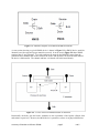
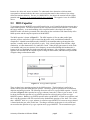
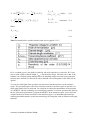
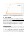
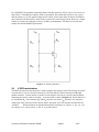
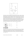
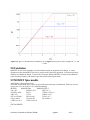
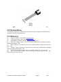
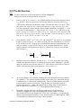
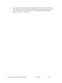
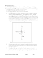
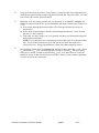
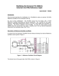
Laboratory Experiment 5 EE348L B.Madhavan Revised by: Aaron Curry University of Southern California. EE348L page1 Lab 5 Table of Contents 5 Experiment #5: MOSFETs Static Operation.............................................................. 4 5.1 Introduction ............................................................................................................................... 4 5.2 Theory........................................................................................................................................ 4 5.2.1 MOSFET Basics ....................................................................................................................... 4 5.3 MOS Capacitor ........................................................................................................................... 6 5.4 MOSFET................................................................................................................................... 7 5.5 Biasing a MOSFET ................................................................................................................. 10 5.6 A MOS current mirror ............................................................................................................. 11 5.7 MOSFET simulation in HSpice ............................................................................................... 13 5.8 Conclusion............................................................................................................................... 16 5.9 MOSFET Spice models........................................................................................................... 16 5.10 Revision History ..................................................................................................................... 17 5.11 References ............................................................................................................................... 17 5.12 Pre-lab Exercises ..................................................................................................................... 18 5.13 Lab Exercises.......................................................................................................................... 20 University of Southern California. EE348L page2 Lab 5 Table of Figures Figure 5-1: Schematic diagram of an NMOS and PMOS transistor. ................................................. 5 Figure 5-2: A cross-section of NMOS transistor in saturation............................................................ 5 Figure 5-3: A P-type MOS Capacitor. ................................................................................................ 6 Figure 5-4: Simulated ID-VDS characteristics of an n-channel MOSFET, 2N7000, for different gate to source voltages. ......................................................................................................... 10 Figure 5-5: Biasing a MOSFET. ........................................................................................................ 11 Figure 5-6: MOS current mirror. ........................................................................................................ 12 Figure 5-7: HSpice netlist for obtaining I-V characteristic of an n-channel MOSFET, 2N7000……... 14 Figure 5-8: ID-VDS characteristics of MOSFET m1 in Figure 5-7for gate to source voltages of 2, 3, and 4 volts. …….......................................................................................................... 15 Figure 5-9: gm versus VDS characteristics of MOSFET m1 in Figure 5-7 for gate to Source voltages of 2, 3, and 4 volts. …………........................................................................ 16 Figure 5-10: Pin diagram of the 2N7000 (Courtesy of Fairchild Semiconductor). ............................. 17 Figure 5-11: Circuit schematic for Laboratory experiment 5 exercise 1 ............................................ 20 University of Southern California. EE348L page3 Lab 5 5 Experiment #5: MOSFETs Static Operation 5.1 Introduction Transistors are at the heart of integrated circuit design. As active elements, they are capable of implementing gain stages, buffers, electrically operable switches, op-amps, and a host of other applications. The word active refers to the fact that transistors require static power from a power supply in order to operate. For amplifiers, the static power is consumed so that the input signals may be amplified. Thus, when a transistor-amplifier provides gain, it means that the signals experience gain at the expense of static power consumption. The most common commercial transistor today is the Metal-Oxide-Semiconductor Field-Effect Transistor (MOSFET). Even though the MOSFET was conceived before the bipolar transistor, it wasn’t until mature fabrications techniques and the digital revolution that the MOSFET became the dominant transistor used today. Even though the MOSFET has been primarily used as a digital device, it has made significant contributions to analog circuit design in recent times despite its relatively poor transconductance compared to the Bipolar Junction Transistor (BJT), primarily due to the needs for mixed signal circuits driven by integration of multiple functions on a single IC. For the next couple labs, the operation of a MOSFET, as used in analog circuit applications, will be presented. This experiment will deal with dc operation conditions, a.k.a. biasing, or quiescent state. As will be seen, the MOSFET can be biased in one of three fundamental regions. This biasing will determine the linearity of the MOSFET. Later labs we will be using MOSFETs as amplifiers that amplify a sinusoid; however, they will only work if correctly biased. 5.2 Theory 5.2.1 MOSFET Basics The MOSFET comes in two varieties, namely, NMOS and PMOS. This lab will primarily deal with NMOS devices. It should be noted that all equation presented for the NMOS transistor are valid for the PMOS device, as long as all the voltage polarities and current directions are switched. As stated above, the MOSFET must be biased in the proper regime in order for it to be used as an amplifier, so this will be the fundamental focus of this lab. The schematic diagrams of an NMOS and PMOS are presented in Figure 5-1. University of Southern California. EE348L page4 Lab 5 Figure 5-1: Schematic diagram of an NMOS and PMOS transistor A cross-section showing a typical NMOS device is shown in Figure 5-2 (a PMOS device would be identical, but with n-type and p-type materials reversed). It can be seen in Figure 5-2 that a NMOS transistor has a P type substrate. To avoid confusion, the name for the MOSFET comes from the generated carrier channel that occurs between the source and the drain, not from the bulk material the device is fabricated in. The channel and how it is formed will be discussed shortly. Figure 5-2: A cross-section of NMOS transistor in saturation. Functionally, the drain, gate and source terminals are the equivalents of the bipolar collector, base and emitter, respectively. However, the MOS device is symmetric, so there is no physical difference University of Southern California. EE348L page5 Lab 5 between the drain and source terminals! To understand what determines which terminal corresponds to drain and which to the source, an investigation must be done on how a bias voltage affects the transistor behavior. For now, in a NMOS device, the drain is the terminal will the higher potential and the source is the terminal with the lower potential. The opposite is true for a PMOS device. 5.3 MOS Capacitor To investigate how the MOSFET reacts to different biasing, we will simplify the device structure into a simple MOS capacitor. The MOS capacitor has the exact same structure as the MOSFET, but without the source and drain. As an understanding of this simplified model is developed, the complete MOSFET model will then be presented with a discussion on the correlation of the functionality of the MOS capacitor and the complete operation of the MOSFET. The MOS capacitor is shown in Figure 5-3. The MOS capacitor is like any other parallel plate capacitor you have seen before. It gets its name from the metal, oxide, semiconductor sandwich it is comprised of. It should be noted that in today’s MOSFETs, the metal that makes up the top plate of the capacitor is actually made out of poly-silicon, or poly. Poly is heavily doped silicon that has a high conductivity, so it has characteristics very much like a metal. Under the poly gate contact is oxide. Oxide is an insulator, and just as in a capacitor, at low frequency no current flows through this insulator (this is because of the very high band gap voltage associated with insulators). Like a capacitor, a positive voltage applied to one terminal leads to a deposit of positive charge on that terminal, and induces an equal amount of negative charge on the other terminal. Figure 5-3: A P-type MOS Capacitor. There are three basic operating regimes for the MOS capacitor. The biasing that is applied to it dictates which regime the MOS capacitor operates. The three regions of operation are: accumulation, depletion and strong inversion. The following discussion will be for a p-type MOS capacitor. It can be seen that in Figure 5-3 the capacitor has a p-type substrate; hence this is where it gets its name. It will be shown later that the operation of p-type MOS capacitor has a direct bearing on how an n-type MOSFET operates. Both the p-type MOS capacitor and n-type MOSFET are built in a p-substrate, and this is why the operation of the first correlates to the fundamental operation of the latter. The reason that a MOSFET built in a p-type substrate is called an n-type MOSFET is because an n-type channel is formed under the gate, more on this later. The thing to remember at this point is to be careful and not to confuse the operation of a p- type capacitor and a p-type MOSFET. The accumulation region University of Southern California. EE348L page6 Lab 5 will be the first region that will be addressed in a p-type capacitor. We assume that the Bulk terminal is grounded and that the Gate voltage is with respect to ground. The “accumulation” region results when the biasing voltage is less than zero, VG < 0. Since a negative potential is put on the metal gate just above the thin oxide, holes are attracted from the bulk to the oxide and start to pile up, or “accumulate” a channel of holes at the oxide interface. The “depletion” region is reached when the voltage applied to the gate is greater than zero, yet less than the threshold voltage of the device, 0 < VG < Vth, where Vth is the threshold voltage. In the depletion region, the gate voltage is not great enough to attract any significant number electrons from the substrate. As the positive gate bias is increased, the holes that are located at the oxide interface are pushed away from the oxide. Thus creating a “depleted” channel of the majority carriers, holes, and creating a channel of fixed ions. As the gate voltage is increase, the minority carriers, electrons, start getting pulled to the oxide layer form the substrate. This continues until the device threshold is met. The device threshold voltage, Vth, is defined as the voltage it takes to “invert” the channel under the oxide of a p-type capacitor to an n+ concentration. At this point, the MOS capacitor has reached “inversion”, VG > Vth. This condition is known as inversion because the applied bias has attracted enough minority carriers, electrons, that the area directly under the oxide looks like an n-material, thus it is inverted. One may ask, what is the difference between inversion and depletion? In inversion the bias on the gate is large enough to attract a large and significant number of electrons, so the surface under the oxide is thus inverted from the original, unbiased, p+ concentration to an n+ concentration. 5.4 MOSFET A cross section of a MOSFET was shown in Figure 5-2. It can be seen that a MOSFET is nothing more than a MOS capacitor with a source and drain at either end. Since half of the MOSFET structure was explained earlier, a discussion of how the drain and source contribute to the functionality of the transistor will be presented. A simplified way of thinking about the operation of a NMOS is to compare it to a switch. When the switch is “on” conduction needs to occur and thus current flows between two contacts. If the switch is “off”, then no current flows and the switch behaves like an open circuit. Think of the gate as an electrically activated switching lever and the source and drain as two contacts that just happen to be heavily doped n-type material. Since the source and drain are comprised of n-type material, electrons must be transported from source to drain for current to flow between them. Remember a MOS capacitor with a gate bias that is equal or less than zero has a channel of holes at the oxide interface, thus the same bias effectively places a barrier, a channel of holes, between the source and drain of a NMOS. These holes block the transport of electrons and thus block the flow of current. Thus, when the NMOS has a gate bias voltage that is equal or less than zero the transistor acts like a switch that has been turned “off”. To turn the transistor “on”, one needs to clear a path in the p-type substrate so electrons can flow from the source to the drain. Going back to the operation MOS capacitor, if a large enough positive bias is applied to the gate, then an inverted channel forms and becomes this desired path. Once the path is created, an electric field from drain to source is needed to sweep the electron through the path. Thus, two bias conditions must be met for the MOSFET to properly be turned “on”. The picture gets a little more complicated when one considers the effect of the drain voltage. Ideally we would like only the gate terminal to influence the current, thus the device would act like an ideal current University of Southern California. EE348L page7 Lab 5 source from the perspective of the source and drain. Ideally, in the sense that this current source, which is connected from drain to source, doesn’t depend on the voltage across it. In actuality, the drain voltage impacts the current, but hopefully to a much lesser extent than the gate voltage. From earlier discussions of diode, it should be clear that if the source sits at ground and the drain is at some positive voltage, there will be a depletion region around the drain (note that the drain and substrate form a pn junction). This depletion region wants to form all around the drain to where the drain meets the oxide; since the inverted channel exists between source and drain, the result is that the depletion region pinches off the channel right near the drain for gate-to-drain voltages less than the threshold voltage (i.e., Vdg > -Vth). Pinch-off is highlighted in Figure 5-2. As the drain voltage is increased, the depletion region extends farther from the drain, shortening the channel length. The obvious question is how do electrons travel from source to drain if the channel doesn’t extend the entire way? The answer is that electrons are swept from the channel to the drain by the strong electric field associated with the depletion region. Since the biasing regimes were discussed for the MOS capacitor, they will now be presented for the MOSFET. To be sure, they are not the same. The biasing of the MOSFET depends on two voltages, namely the gate-to-source and the drain-to-source voltages. When dealing with analog circuits, one must ensure the biasing is correct for the desired operation, which more often than not is the saturation ( o r l i n e a r ) region. There are three region of operation for the MOSFET: cut-off, triode (a.k.a. ohmic), and saturation. These three regions are determined by the two biasing conditions stated above. Going back to the switch analogy, the gate-source voltage determines if the device is “on” or “off”. Cut-off occurs when the gate-source voltage is less than the device threshold voltage, Vgs < Vth. If the device is in cut-off, the drain current, Id, is approximately zero and the device is considered off. This condition is independent of the drain-to-source voltage. Now the truth of the matter is the MOSFET doesn’t act like a perfect switch that turns off and on. Current does flow in sub-threshold gate biasing, but for the purposes of this lab it will be assumed the drain current is small and approximately zero when Vgs<0. The other two stages of operation assume the gate-source biasing is above threshold (Vgs>0) and depend on the biasing of the drain-source. The equations describing exactly how drain-source voltage influences channel charge (and in turn the current) are incredibly complicated. However, simplified analysis shows that the current depends roughly on the square of the gate voltage for Vds ≥ Vgs -Vt (saturation region), and roughly linearly for Vds < Vgs -Vt (triode region). This assumes the devices are large enough to avoid velocity saturation. Be careful not to confuse the linear current dependence of the triode region with the linear operation of the device. When one talks about the linear operation of the device, they are referring to the small-signal dynamic operation. This occurs when the transistor is biased in the saturation region. Simulated iD versus vds curves for multiple vgs voltages for a discrete nchannel MOSFET device, 2N7000, are shown in Figure 5-4. One can see the two different operating conditions the MOSFET experiences as Vds is swept, namely the triode and the saturation regions. A summary of the three different operating regions and the associated drain current in each is presented below for the NMOS. The equations below also hold for the PMOS transistor if the polarity of all voltages is flipped. (Note: The threshold voltage, Vtp, for a PMOS is negative.) NMOS: I d 0, University of Southern California. EE348L V gs Vtn page8 (cut-off) (5.1) Lab 5 V W I d K n Vds V gs Vtn ds 1 nVds , 2 L V gs Vtn K W 2 I d n V gs Vtn 1 nVds , 2 L V gs Vtn (triode) (5.2) (saturation) (5.3) 0 Vds V gs Vtn Vds V gs Vtn Where K n n cox c ox (5.4) ox (5.5) t ox Table 5.1 summarizes the variables and their units used in equation 5.1-5.5. Table 5-1: MOSFET parameters Kn is a constant given by the product of mobility and oxide capacitance per unit area, W/L is the ratio of oxide width to channel length, Vtn is the threshold voltage. One final note is that if the substrate is at a different voltage than the source, the threshold voltage varies due to the pn junction between source and bulk. For this lab, the source and bulk will be tied together, so this effect will be ignored. To recap, for small-signal linear operation, one must ensure that the transistor is in the saturation region. The goal and purpose of this lab is to bias the transistor in the linear region of operation, so a small signal analysis may be preformed. Be careful not to confuse the nomenclature of the operation of a MOSFET with the terminology used with bipolar transistor. For linear operation, thus allowing the use of the small signal models, you want the MOSFET in the saturation region, yet you will learn in future labs that you do not want a BJT in the saturation region. It is unfortunate and sometimes confusing that both transistors use the same terminology for biasing that yields in different small signal operation. University of Southern California. EE348L page9 Lab 5 Figure 5-4: Simulated ID -V DS characteristics of an n-channel MOSFET, 2N7000, for different gate to source voltages. 5.5 Biasing a MOSFET Transistors need to be biased to the appropriate level in order to operate correctly. The small signal model circuit that designers use is only valid if the transistor is biased properly. This section will cover the biasing of an n-channel MOSFET amplifier shown in Figure 5-5. The n-channel MOSFET is to be biased in the saturation region, at an operating point of desired drain current, drain voltage, and gate voltage. The use of the quadratic relationship (equation 5.3) requires knowledge of the mobility, oxide capacitance per unit area, the width and length of the device, and the threshold voltage. For discrete components, these values vary too much for the quadratic relationship to be a good predictor. One can measure these quantities in the laboratory, but the idea here is to get a design that works without knowing all of the device parameters beforehand. For this example, let us assume that we looked up the data sheet of a discrete MOSFET device that we are interested in, and determined that its threshold voltage, Vth, is in the range of 1V-to-3V. Remember that Vgs must exceed the threshold voltage, Vth, for current to flow. Say we desire a drain current of 1mA. We assume Vth = 3.0V (worst case Vth in range of 1V-3V). We set Vgs = 3.25V so that we have Vgs- Vth = 0.25V of worst-case gate-source overdrive voltage. Next, a 3.75V gate voltage is arbitrarily chosen. Given that we want Vgs = Vg–Vs= 3.25V, this dictates that Vs=0.5V. Using Ohm’s law, we get the source resistance, Rss = 0.5V/1mA = 500Ω. Making sure the condition for saturation, Vds>= Vgs-Vth, is satisfied, the drain voltage is chosen to be 3.5V (Vds = 3.5V – 0.5V = 3.0V). With a supply voltage, Vdd=5V, and drain current of 1mA, this requires a 1.5kΩ resistance (Rd) between the supply and the drain terminal. Next, in order to set the gate voltage to at 3.75V, we use a voltage divider as shown in Figure 5-5 to derive Vg = 3.75V from the supply, Vdd=5V. The resistor ratio of Rb1: Rb2 needs to be 1:3. Therefore we set Rb1=1kΩ and Rb2=3kΩ. Note that the bias network requires 1.25mA from the 5V supply! University of Southern California. EE348L page10 Lab 5 For a MOSFET, the quadratic relationship dictates that the sensitivity of Id to Vgs is not as severe as that of the I-V relationship of a diode, which is exponential. This means that Vgs has to vary a great deal more than say, Vb, the applied voltage across a diode, for the same range of currents. Sometimes, due to tolerances in fabrication, it can be tricky to achieve the exact biasing current. However, a simple solution is to make one of the gate resistors, say Rb2, a potentiometer. This allows one to tune and monitor the desired MOSFET performance. Figure 5-5: Biasing a MOSFET. 5.6 A MOS current mirror The MOS current mirror discussed here is used to properly bias analog circuits. The strategy invoked in a current mirror is to set a desired current, Iref, in one side and have that current mirrored through another transistor. Current mirrors are used in circuit design so one can set a specific current without disturbing the circuitry it that it is biasing. A current mirror is shown in Figure 5-6. Notice that Iref is set in transistor M1, since transistor M1 and M2 have the exact same Vgs, then the two transistors conduct the same amount of drain current. Hence Iref equals Iout. This assumes the transistors are “matched”. When transistors are matched, then all their parameters are equal (i.e. µn, cox, etc.). An analysis of a current mirror is left as a pre-lab exercise. University of Southern California. EE348L page11 Lab 5 Figure 5-6: MOS current mirror. Note that M1 is a diode-connected transistor which guarantees that it operates in saturation, so long as the gate voltage lies at least a threshold voltage above ground. The idea is that R is chosen to establish the desired reference current in M1, and then M2 simply mirrors this current exactly, as M1 and M2 have identical effective gate-source voltages (i.e., Vgs – Vt is identical for both). In IC design, one has the additional benefit of being able to scale the reference current by choosing M2 to have a larger gate aspects ratio (W/L) than the reference. In the lab we use discrete components with fixed dimensions, so this seems like it would present some difficulty when larger (W/L) ratios are desired. However, one may achieve a larger ratio by paralleling devices. Some drawbacks to this approach include taking up a lot of space and being limited to integer multiples of the reference current. The major problem with this current source (in the lab and in IC design) lies in the dependence of the currents on Vds, which differs for each device. Analysis of this current mirror leads to: Vdd I ref R V g1 K W 2 I ref n1 V g1 Vt 1 1V g1 2 L K W 2 I out n 2 V g1 Vt 1 2Vds2 2 L I ref K 1 1V g1 n1 I out K n 2 1 2Vds2 (5.6) (5.7) (5.8) (5.9) Thus, the ratio is not 1:1 as is hoped. In IC design, the Kn factors will be very close, as matching is a strong point of IC fabrication processes. However, in the lab and in IC design, regardless of whether the lambda terms are equal, the drain-source voltages are necessarily different for different drain resistances, making it impossible to match the currents over a wide range of loads. In the lab, you will use a potentiometer for the load, and observe the variation in current as the load, and hence the drainsource voltage, varies. University of Southern California. EE348L page12 Lab 5 5.7 MOSFET simulation in Spice In this section, we investigate the simulation of the I-V characteristics of 2N7000, a discrete n-channel MOSFET, whose datasheet may be found at (http://www.supertex.com ). The syntax (see page 8-14 of the HSpice Device Models Reference Manual, version 2001.4, December 2001) for a MOSFET element in HSpice is: mxxx drain gate source bulk mosfet_model_name W=mosfet_width L=mosfet_length Where drain, gate, source, bulk are the drain, gate, source and bulk terminals of the MOSFET mxxx, and mosfet_model_name is the model name of the MOSFET as specified in the HSpice MOSFET model deck. Wand Lare the width and length of the MOSFET respectively, specified in units of meters. The simulation of semiconductor devices requires the specification of an appropriate device model deck in Spice. The model deck specifies a particular mathematical model of the device being simulated and the values of the parameters associated with the model. Model parameter values that are not specified default to the default values specified in Spice. The interested reader can determine the default values associated with a particular model by searching the HSpice Device Models Reference Manual, version 2001.4, December 2001. An example of an HSpice model deck specification for 2N7000, the discrete n-channel MOSFET used in this laboratory assignment, is shown below. The model deck is obtained from www.supertex.com. Note that the model deck starts with the keyword .MODEL, followed by the particular n-channel MOSFET model name, 2N7000, followed by the keyword NMOS. The “+” character is a continuation character that indicates that the model deck specification continues on that line. .MODEL NMOS2N7000 NMOS(LEVEL=3 +Rs=.205 NSUB=1.0e15 DELTA=.1 +KAPPA=.0506 TPG=1 CGDO=3.1716e-9 +RD=.239 VTO=1 VMAX=1.0e7 +ETA=.0223089 NFS=6.6e10 TOX=1.0e-7 +LD=1.698e-9 UO=862.425 XJ=6.4666e-7 +THETA=1.0e-5 CGSO=9.09e-9) Very Important point: It is very important to start the model deck with the .MODEL keyword, followed by the mosfet model name and then the keyword NMOS for an n-channel MOSFET. It is good practice to put the device models at the end of the netlist before the final .END statement. Figure 5-7 is an example of a netlist that can be used to plot the ID-VDS characteristics of the MOSFET 2N7000, specified by the model deck named 2N7000. The drain to source voltage, VDS, is swept from 0V through 5V in steps of 0.01V at gate to source voltages, vGS, of 2V, 3V, and 4V. The Spice simulation results are shown in Figures 5-8 and 5-9. MOSFET I-V characteristic *Written Feb 24, 2005 for EE348L by Bindu Madhavan. *Edited for P/LTSPICE Feb 24, 2012 by Aaron Curry. ****************************************************** ****options section ****************************************************** .opt post University of Southern California. EE348L page13 Lab 5 ****************************************************** **** circuit description ****************************************************** m1 drain gate 0 0 NMOS2N7000 w=.8e-2 l=2.5e-6 ****************************************************** **** sources section ****************************************************** vdrain drain 0 5V vgate gate 0 1V ****************************************************** **** specify nominal temperature of circuit in degrees C ****************************************************** .TEMP=27 ****************************************************** **** analysis section ****************************************************** .op .dc vdrain 0 5.0 0.01 sweep vgate poi 3 2 3 4 ****************************************************** ****probe statement section ****************************************************** *see pages 8-63 to 8066 of HSpice user manual, Version 2001.4 .probe dc idrain =par(‘id(m1)’) .probe dc gm =par(‘lx7(m1)’) .probe dc gmb =par(‘lx9(m1)’) .probe dc ro =par(‘1/lx8(m1)’) ****************************************************** **** models section ****************************************************** .MODEL NMOS2N7000 NMOS(LEVEL=3 +Rs=.205 NSUB=1.0e15 DELTA=.1 +KAPPA=.0506 TPG=1 CGDO=3.1716e-9 +RD=.239 VTO=1 VMAX=1.0e7 +ETA=.0223089 NFS=6.6e10 TOX=1.0e-7 +LD=1.698e-9 UO=862.425 XJ=6.4666e-7 +THETA=1.0e-5 CGSO=9.09e-9) * w=.8e-2 l=2.5e-6. MAKE SURE THIS IS SPECIFIED IN INSTANTIATION *2N7002 MODEL * .end Figure 5-7: Spice netlist for obtaining I-V characteristic of an n-channel MOSFET, 2N7000. University of Southern California. EE348L page14 Lab 5 Figure 5-8: ID-VDS characteristics of MOSFET m1 in Figure 5-7 for gate to source voltages of 2, 3, and 4 volts. University of Southern California. EE348L page15 Lab 5 Figure 5-9: gm-VDS characteristics of MOSFET m1 in Figure 5-7 for gate to source voltages of 2, 3, and 4 volts. 5.8 Conclusion MOSFETs are the most commonly used semiconductor today in integrated circuit design. A circuit designer must bias the MOSFET correctly to ensure small-signal linear operation. If not biased properly, distortion will hinder the design. The next lab will assume that the MOSFET is biased in the saturation region and deal primarily with dynamic operation and the small-signal model. 5.9 MOSFET Spice models *(this Model is from supertex.com) *Note that usually the W and L values are specified when a transistor is instantiated. Make sure you use *proper size of w=.8e-2 and l=2.5e-6 when instantiating. .MODEL NMOS2N7000 NMOS(LEVEL=3 +Rs=.205 NSUB=1.0e15 DELTA=.1 +KAPPA=.0506 TPG=1 CGDO=3.1716e-9 +RD=.239 VTO=1 VMAX=1.0e7 +ETA=.0223089 NFS=6.6e10 TOX=1.0e-7 +LD=1.698e-9 UO=862.425 XJ=6.4666e-7 +THETA=1.0e-5 CGSO=9.09e-9) * *2N7002 MODEL * University of Southern California. EE348L page16 Lab 5 Figure 5-10: Pin diagram of the 2N7000 (Courtesy of Fairchild Semiconductor). 5.10 Revision History This laboratory experiment is a modified version of the laboratory assignment 5 (MOSFET Static Operation) created by Jonathan Roderick. 5.11 References [1] Pspice user manual. Course website: www.jcatsc.com [2] LTSpice user manual. Course website: www.jcatsc.com [3] Bindu Madhavan, EE348L Laboratory Experiment 2, Spring 2012. [4] Gerald W. Neudeck. Volume II The PN Junction, Addison-Wesley Publishing Company, Reading, Massachusetts, 1989. [5] Ben G. Streetman. Solid State Electronic Devices. Prentice-Hall Inc., Englewood Cliffs, New Jersey, 1990. [6] Richard C. Jaeger. Introduction to Microelectronic Fabrication. Addison-Wesley Publishing Company, Reading, Massachusetts, 1993. [7] S. M. Sze. Physics of Semiconductor Devices. John Wiley & Sons, Inc., New York, 1981. [8] Paul R. Gray & Robert G. Meyer. Analysis and Design of Analog Integrated Circuits. John Wiley & Sons, Inc., New York, 1993. University of Southern California. EE348L page17 Lab 5 5.12 Pre-lab Exercises Note: • • For Spice simulations, use the model deck for 2N7000 in Figure 5-7 Submit plots relevant to each question in your pre-lab. 1) If given a plot of √ID versus VGS for a NMOS transistor biased in the saturation region, Cox, and W/L, derive an expression to calculate the mobility of electrons [cm2/Vs], µn. Could you also determine the threshold voltage, Vth, from this data? If so, how? Hint: the square law equation for a saturated transistor is only valid for Vgs>Vth. For both calculations assume that the channel length modulation is negligible, i.e., λn=0 in equation 5.2 and equation 5.3. Now, Plot the √I D verus V G S for a 2N7000 usin g Spice. Sweep V G S from 0 -3V and set V D S =5V. With this plot, calculate Vth and µn for the given Spice model of the 2N7000 . From the model we can see that tox=1e-5 cm, W=8e-3m, and L=2.5e -6m. 2) Given Kn(W/L)=5E10-3 A/V2, Vth=1.2V, and λn=0.002V-1 use Excel, or an equivalent, to plot ID versus VGS for VDS = 5V. Make sure data points are calculated for VGS from 0V to 5V in steps of 0.25V. Using the plot so obtained, determine the transconductance, gm [mS], for each ∆VGS region of 0.25V from 0V to 5V, using the equation below. Set any negative values to 0 (this should occur when VGS is below Vth). Plot gm versus the gatesource voltage VGS. gm 3) I ds V gs Vds cons tan t I I d1 d2 V V gs1 gs2 Vds cons tan t Repeat pre-lab exercise number 2, but now let VDS = 7V. Now, using these values along with the ones obtained in exercise 2, calculate the drain-to-source conductance, gds [mS], using the equation below for each value of VGS. Now, take the inverse of these values to obtain ro (the output resistance of the transistor). Plot ro versus VGS. g ds I ds Vds Vgs cons tan t I I d1 d 2 V V ds1 V cons tan t ds2 gs 4) As a circuit designer, it is sometimes advantageous to find the optimum biasing condition for a MOSFET. The optimum biasing condition occurs when gm is maximized and gds is minimized (or ro is maximized) simultaneously. This occurs when intrinsic gain of the transistor which is gm*ro is maximized. Using the data you calculated to plot the intrinsic gain versus VGS. What is the optimal biasing voltage range for the transistor? Hint: this should occur right after VGS > Vth and diminish with increasing VGS. 5) Using Spice, simulate and verify the biasing example that was presented for a MOSFET in Figure 5-5. Is the current through the transistor within ±2% of the specifications the circuit was designed for? If not, why? Now adjust VGS by adjusting Rb2 until the current through the transistor is 1mA. Record the new VG that is required. Hint: You should have to adjust the circuit to get correct operation. University of Southern California. EE348L page18 Lab 5 6) Using Spice, simulate the current mirror from Figure 5-6. Set R to 1k ohms and Vdd to 5 volts. Sweep Vout from 0V-5V and plot Iout and Iref on the same plot. Over what values of Vout is M2 saturated? Can you see the effects of channel length modulation? What happens to Iout when Vout=vgs? Why? University of Southern California. EE348L page19 Lab 5 5.13 Lab Exercises Note: IT IS VERY IMPORTANT that you do not exceed 200mA of drain current while taking measurements. If increasing Vgs increases the current beyond 200mA, STOP increasing Vgs. When applying Vgs and Vds, You should do so slowly. Do not set them and turn them on abruptly. See Figure 5-7 for HSpice MOSFET model deck for 2N7000. Submit plots relevant to reach question in your lab report. Refer to Figure 5-10 for the correct pin orientation of the 2N7000. 1) In pre-lab problem 1, you derived expressions to calculate the mobility of electrons [cm2/Vs], µn, and the threshold voltage, Vth, from a graph of √ID versus VGS. Build the circuit in Figure 5-11 with VD=5V and Rss=50Ω, and measure ID while varying VGS from 05V in .25V increments. Plot your results, and calculate µn and Vth for this transistor using the data collected. From the Spice netlist provided in Figure 5-7, it can be seen that the 2N7000 MOSFET has W=8000 µm, L=2.5 µm, and Tox= 1e-5 cm. How close are the measured values to the values found in the pre-lab? Hint: it is very likely that the threshold voltage does not match the value obtained in the pre-lab. Figure 5-11: Circuit schematic for Laboratory experiment 5, exercise 1 2) Using your results from lab exercise 1, repeat pre-lab problem 2 but with measurements instead of calculations. Calculate and plot gm versus VGS. How do your plots compare to those in pre-lab problem 2? 3) Using Figure 5-11, repeat pre-lab problem 3 but with measurements instead of calculations. Set VD to 7V and sweep VGS from 0V-5V in .25V increments. Calculate and plot ro versus VGS. How do your plots compare to those in pre-lab problem 3? University of Southern California. EE348L page20 Lab 5 4) Using the results from lab exercises 2 and 3 above, use the procedure in pre-lab problem 4 to determine the optimal biasing voltage range from measured data. Plot your results. For what bias current is the intrinsic gain maximized? 5) Build and verify the biasing example that was presented for a MOSFET in Figure 5-5. Instead of using a resistor for Rb2, use a potentiometer and adjust it until the gate voltage is at 3.75V. A) Is the current through the transistor within ±2% of the specifications the circuit was designed for? B) If not, adjust the potentiometer until the current through the transistor is 1mA. Record the new VGS that is required. C) From what you have learned, can you speculate why there were discrepancies between theory and measured data? NOTE: It is a good idea to use a potentiometer for biasing the gate of a transistor in these labs. This is because each device varies from part to part and so the required VGS required will vary. Tuning a potentiometer is much easier than swapping resistors! 6) Now, build the current mirror from Figure 5-6. Set R to 1k ohms and Vdd to 5 volts. Sweep Vout and measure Iout. Also, record the gate/drain voltage of m1 and Iref. Plot your results using excel or similar. Include on your plot the Iref level. Over what values of Vout is M2 saturated? How well does it mirror the current in M1? What are some possible explanations if it does not mirror the current well? University of Southern California. EE348L page21 Lab 5