1
3.0 INSTALLATION:
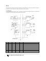
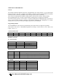
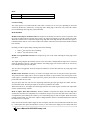
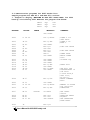
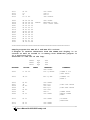
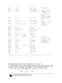
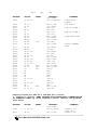
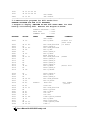
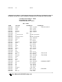
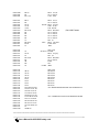
Please refer the below table for connection procedure for various trainer
kits.
Sl. No
Model No.
1
MPS 85-3
Studycard
Adapter
No Adapter
Connection Procedure
2
ESA 85-2
No Adapter
3
ESA 86/882
Study card adapter
for
ESA 86-2/3
trainer
4
ESA 86/883
Study card adapter
for
ESA 86-2/3
trainer
Connect 50 pin FRC cables between J1, J2 of the adapter
with J1,J2 of the trainer kit.
Connect 26 pin FRC cables between J3,J4 of the adapter with
J3,J4 of the study card respectively.
5
ESA 86E
No Adapter
6
ESA 31
Study Card adapter
ESA 31/51 Trainer
7
ESA 51
Study Card adapter
ESA 31/51 Trainer
8
ESA 51E
ESA 51E Study
card adapter.
Connect 26 pin FRC cables between J3, J4 of study card with
J6 ,J7 of the trainer kit respectively.
Connect 50 pin FRC cable between J1 of adapter with J5 of
the trainer kit.
Connect 26 pin FRC cables between J3,J4 of adapter with
J3,J4 of the study card respectively.
Connect 50 pin FRC cable between J1 of adapter with J1 of
the trainer kit.
Connect 26 pin FRC cables between J3,J4 of adapter with
J3,J4 of the study card respectively.
Connect 50 pin FRC cable between P3 of adapter with P1 of
study card.
Connect 26 pin FRC cables between J3 ,J4 of adapter with
J4,J6 of the trainer kit respectively.
Connect 26 pin FRC cables between J3, J4 of study card with
J3 ,J4 of the trainer kit respectively.
Connect 50 pin FRC cable between P1 of study card with P1
of the trainer kit .
Connect 50 pin FRC cables between J1, J2 of the adapter
with J1,J2 of the trainer kit.
Connect 26 pin FRC cables between J3,J4 of the adapter with
J3,J4 of the study card respectively.
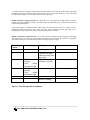
The 8251A programmable communication interface
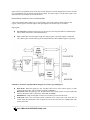
The 8251A is a programmable chip designed for synchronous and a synchronous serial data communication,
packaged in a 28 – pin DIP. The 8251A is the enhanced version of its predecessor, the 8251, and it is
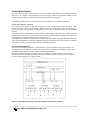
compatible with the 8251. Figure1 shows the block diagram of the 8251A. It includes 5 sections: Read/Write
Control Logic, Transmitter, Receiver, Data Bus Buffer, and Modem Control.
The control logic interfaces the chip with the MPU, determines the function of the chip according to the
control word in its register (to be explained below), and monitors the data flow. The transmitter section
converts a parallel word received from the MPU into serial bits and transmits them over the TxD line to a
peripheral. The receiver section receives serial bits from a peripheral, converts them into a parallel word, and
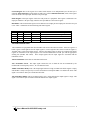
transfers it to MPU. The 8251A is a complex device capable of performing various functions. For the sake of
clarity, this chapter focuses only on the asynchronous mode of serial I/O, and excludes any discussion of the
synchronous mode and the modem control. The asynchronous mode is often used for the data communication
between the MPU and serial peripherals such as terminals and floppy disks.
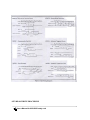
User’s Manual for 8251/8253 study card
2