1
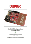
LPC-P1343 development board
user's manual
All boards produced by Olimex are ROHS compliant
Revision C, February 2013
Copyright(c) 2011, OLIMEX Ltd, All rights reserved
INTRODUCTION
LPC-P1343 is a development board with LPC1343 ARM Cortex-M3 based
microcontroller for embedded applications from NXP. LPC-P1343 featuring a high
level of integration and low power consumption. This microcontroller supports
various interfaces such as one Fast-mode Plus I2C-bus interface, USB, UART, SSP interfaces, four general purpose timers, a 10-bit ADC. On the board are available
UEXT, Debug Interface, user buttons, USB device and user LEDs. This allows you to
build a diversity of powerful software that can be used in a wide range of applications.
BOARD FEATURES
•
MCU: LPC1343 Cortex-M3, up to 70 MHz, 32 kB Flash, 8kB SRAM,
UART RS-485, USB, SSP, I2C/Fast+, ADC
•
Power supply circuit
•
Power-on led
•
USB connector and functionality
•
USBC LED
•
Debug interface – SWD (Serial Wire Debug)
•
UEXT connector
•
Eight user LEDs
•
Two user buttons
•
Reset button
•
Prototype area
•
FR-4, 1.5 mm, red soldermask, white component print
•
Dimensions:80x50mm (3.15 x 1.97")
ELECTROSTATIC WARNING
The LPC-P1343 board is shipped in protective anti-static packaging. The board
must not be subject to high electrostatic potentials. General practice for working
with static sensitive devices should be applied when working with this board.
BOARD USE REQUIREMENTS
Cables: The cable you will need depends on the programmer/debugger you use.
For instance, if you use https://www.olimex.com/Products/ARM/JTAG/ARMJTAG-COOCOX/, you will need USB A-B cable.
Hardware: Programmer/debugger or other compatible programming/debugging
tool with SWD interface. The only Olimex programmer that has SWD interface at
the moment is ARM-JTAG-COOCOX –
https://www.olimex.com/Products/ARM/JTAG/ARM-JTAG-COOCOX.
OpenOCD debuggers (ARM-JTAG-TINY, ARM-JTAG-TINY-H, ARM-JTAG-OCD,
ARM-JTAG-OCD-H) can also be adapted to work with SWD interface by getting
https://www.olimex.com/Products/ARM/JTAG/ARM-JTAG-SWD/. NOTE that
at the current moment only Rowley Crossworks supports this combination.
PROCESSOR FEATURES
LPC-P1343 board use ARM Cortex™-M3 microcontroller LPC1343FBD48/301 from
NXP Semiconductors with these features:
–
ARM Cortex-M3 processor, running at frequencies of up to 72 MHz
–
ARM Cortex-M3 built-in Nested Vectored Interrupt Controller (NVIC).
–
32kB on-chip flash programming memory. Enhanced flash memory
accelerator enables high- peed 72 MHz operation with zero wait states
–
In-System Programming (ISP) and In-Application Programming (IAP) via
on-chip bootloader software.
–
Serial interfaces:
- USB 2.0 full-speed device controller with on-chip PHY for device
- UART with fractional baud rate generation, modem, internal FIFO
and RS-485/EIA-485 support.
- SSP controller with FIFO and multi-protocol capabilities.
- I2C-bus interface supporting full I2C-bus specification and Fastmode Plus with a data rate of 1 Mbit/s with multiple address
recognition and monitor mode.
–
Other peripherals:
- 42 General Purpose I/O (GPIO) pins with configurable pullup/down resistors and a new, configurable open-drain operating
mode.
- Four general purpose timers/counters, with a total of four capture
inputs and 13 match outputs.
- Programmable WatchDog Timer (WDT).
- System tick timer.
–
Serial Wire Debug and Serial Wire Trace Port.
–
High-current output driver (20 mA) on one pin.
–
High-current sink drivers (20 mA) on two I2C-bus pins in Fast-mode Plus.
–
Integrated PMU (Power Management Unit) to minimize power
consumption during Sleep, Deep-sleep, and Deep power-down modes.
–
Three reduced power modes: Sleep, Deep-sleep, and Deep power-down.
–
Single 3.3 V power supply (2.0 V to 3.6 V).
–
10-bit ADC with input multiplexing among 8 pins.
–
40 GPIO pins can be used as edge and level sensitive interrupt sources.
–
Clock output function with divider that can reflect the main oscillator clock,
IRC clock, CPU clock, Watchdog clock, and the USB clock.
–
Processor wake-up from Deep-sleep mode via GPIO interrupts.
–
Brownout detect with four separate thresholds for interrupt and one
threshold for forced reset.
–
Power-On Reset (POR).
–
Crystal oscillator with an operating range of 1 MHz to 25 MHz.
–
12 MHz internal RC oscillator trimmed to 1 % accuracy that can optionally
be used as a system clock.
–
PLL allows CPU operation up to the maximum CPU rate without the need
for a high-frequency crystal. May be run from the main oscillator, the
internal RC oscillator, or the Watchdog oscillator.
–
Code Read Protection (CRP) with different security levels.
BLOCK DIAGRAM
MEMORY MAP
red
red
red
R4
10k
red
R5
10k
red
R6
10k
red
3.3V
OUT
R21
390R/1%
R20
240R/1%
100nF
C8
R19
560R
PWR
GND_PIN
GND
+
IT1185AU2
RESET
RSTN
R18
10k
BUT2
T1157
BUT1
T1157
WAKE_UP
http://www.olimex.com/dev
COPYRIGHT(C), 2009
Rev. Initial
BH10S
BH10S
BH10S
BH10S
BH10S
BH10S
BH10S
BH10S
BH10S
BH10S
UEXT
UEXT-1
UEXT-2
TXD
UEXT-3
RXD
UEXT-4
SCL
UEXT-5
SDA
UEXT-6
MISO
UEXT-7
MOSI/SWV UEXT-8
SCK
UEXT-9
CS
UEXT-10
3.3V
LPC-P1343
R17
10k
R15
2.0k
3.3V 3.3V
R16
2.0k
3.3V
LPC1343FBD48
41
44
19
20
33
34
35
39
40
45
46
47
9
17
30
42
VBUS
DD+
ID
GND
USB
R14
560R
47k
R13
1.5k/1%
#USB_CONNECT
USBC
yellow
MICRO_B
C7
10nF
USB_VBUS
DR11
D+
R12
C6
33R
33R
U2DDU2D+
D+
3.3V_CORE_E
44
1
2
3.3V
C4
CLOSE
41
100nF
19
20
RXD
TXD
SWD
WAKE_UP
P1_0
P1_1
P1_2
P1_3
P1_4
P1_5
P1_6
P1_7
P1_8
P1_9
P1_10
P1_11
33
34
35
39
40
45
46
47
9
17
30
42
GND3
GND4
C9
10uF/6.3V/TANT
IN
3.3V
2
13
26
38
18
21
1
11
12
24
25
31
36
37
43
48
RST
P0_1
P0_2
P0_3
SCL
P0_4
SDA
P0_5
#USB_CONNECT P0_6
P0_7
MISO
P0_8
MOSI/SWV
P0_9
SWC
P0_10
P0_11
RSTN
3
4
10
14
15
16
22
23
27
28
29
32
BLD_E
R10 1k
C5
3.3V
T1
DTA114YKA
18p(NA)
ADJ/GND
3.3V
USER
2
13
26
38
18
21
1
11
12
USER 24
CS
25
SCK 31
P2_0
P2_1
P2_2
P2_3
P2_4
P2_5
P2_6
P2_7
P2_8
P2_9
P2_10
P2_11
BUTTONS
36
37
43
48
C3
5
8
6
6
Q1
12MHz/20pF
7
7
P3_0
P3_1
P3_2
P3_3
27pF
C2
5
8
3
4
10
14
15
16
22
23
27
28
29
32
10k HN1x2
10k
1k
18p(NA)
+5V_JLINK
D1
BAT54C
VR1(3.3V)
LM1117IMPX-ADJ
3.3V
3.3V
560R
R4
R3
R2
R1
R-MAT2
560R
R4
R3
R2
R1
R-MAT1
27pF
100nF
C1
USB_VBUS
#RESET/PIO0_0
PIO0_1/CLKOUT/CT32B0_MAT2/USB_FRAME_TOGGLE
PIO0_2/SSEL/CT16B0_CAP0
VDDIO
PIO0_3/USB_VBUS
PIO0_4/SCL
PIO0_5/SDA
PIO0_6/#USB_CONNECT/SCK
VSSIO
PIO0_7/#CTS
PIO0_8/MISO/CT16B0_MAT0
XTALIN
PIO0_9/MOSI/CT16B0_MAT1/TRACE_SWV
TCK/SWCLK/PIO0_10/SCK/CT16B0_MAT2
TDI/PIO0_11/AD0/CT32B0_MAT3
XTALOUT
TMS/PIO1_0/AD1/CT32B1_CAP0
TDO/PIO1_1/AD2/CT32B1_MAT0
PIO3_0
#TRST/PIO1_2/AD3/CT32B1_MAT1
PIO3_1
SWD/PIO1_3/AD4/CT32B1_MAT2
PIO3_2
PIO1_4/AD5/CT32B1_MAT3/WAKEUP
PIO3_3
PIO1_5/#RTS/CT32B0_CAP0
PIO1_6/RXD/CT32B0_MAT0
PIO2_0/#DTR
PIO1_7/TXD/CT32B0_MAT1
PIO2_1/#DSR
PIO1_8/CT16B1_CAP0
PIO2_2/#DCD
PIO1_9/CT16B1_MAT0
PIO2_3/#RI
PIO1_10/AD6/CT16B1_MAT1
PIO2_4
PIO1_11/AD7
PIO2_5
PIO2_6
USB_DM
PIO2_7
USB_DP
PIO2_8
PIO2_9
VDD(3V3)/AVCC/VREF
PIO2_10
PIO2_11/SCK
VSS
U1
R7
R8
R9
USB
USB_VBUS
POWER SUPPLY
3.3V 3.3V
3.3V_IO_E
CLOSE
3.3V
3.3V
GND1
GND2
3.3V 3.3V 3.3V 3.3V
LED0 LED1 LED2 LED3 LED4 LED5 LED6 LED7
red
+5V_JLINK
MOSI/SWV
SWD
SWC
R1
10k
1
red
1
3
5
7
9
11
13
15
17
19
3.3V
2
BH20S
SWD
3.3V
2
1
2
4
6
8
10
12
14
16
18
20
DEBUG INTERFACE:
SCHEMATIC
10k
BOARD LAYOUT
POWER SUPPLY CIRCUIT
LPC-P1343 is power supplied +5V via USB, or via JTAG.
RESET CIRCUIT
LPC-P1343 reset circuit includes LPC1343 pin 3 (#RESET/PIO0_0), R18 (10k) and
RESET button.
CLOCK CIRCUIT
Quartz crystal 12 MHz is connected to LPC1343 pin 6 (XTALIN) and pin 7
(XTALOUT).
JUMPER DESCRIPTION
3.3V_CORE_E
This jumper, when closed, enables microcontroller 3.3V power supply.
Default state is closed.
3.3V(I/O)_E
This jumper, when closed, supplies 3.3 V voltage to LPC1343 pin 8 (VDDIO).
Default state is closed.
BLD_E
If BLD_E is closed during Reset and USB is connected to computer, then removable
disk will appear in My computer. The user can create via IAR "*.bin" file, which can
be placed into the removable disk. After this when you open jumper BLD_E and then
reset the board the microcontroller will execute the program stored in the "*.bin" file.
Default state is open.
INPUT/OUTPUT
LED0 (red) connected via R-MAT1 to LPC1343 pin 36 (PIO3_0).
LED1 (red) connected via R-MAT1 to LPC1343 pin 37 (PIO3_1).
LED2 (red) connected via R-MAT1 to LPC1343 pin 43 (PIO3_2).
LED3 (red) connected via R-MAT1 to LPC1343 pin 48 (PIO3_3).
LED4 (red) connected via R-MAT2 to LPC1343 pin 18 (PIO2_4).
LED5 (red) connected via R-MAT2 to LPC1343 pin 21 (PIO2_5).
LED6 (red) connected via R-MAT2 to LPC1343 pin 1 (PIO2_6).
LED7 (red) connected via R-MAT2 to LPC1343 pin 11 (PIO2_7).
USBC (yellow) shows that USB is connected.
Power-on LED (red) – this LED shows that +3.3V is applied to the board.
User button with name BUT1 (USER) connected to LPC1343 pin 24 (PIO2_9).
User button with name BUT2 connected to LPC1343 pin 40 (WAKEUP).
Reset button with name RESET connected to LPC1343 pin 3 (#RESET/PIO0_0).
EXTERNAL CONNECTORS DESCRIPTION
UEXT
Pin #
Signal Name
1
3.3V
2
GND
3
TXD
4
RXD
5
SCL
6
SDA
7
MISO
8
MOSI/SWV
9
SCK
10
CS
SWD
Pin #
Signal Name
Pin #
Signal Name
1
3.3V
2
3.3V
3
NC
4
GND
5
NC
6
GND
7
SWD
8
GND
9
SWC
10
GND
11
pull-down
12
GND
13
MOSI/SWV
14
GND
15
NC
16
GND
17
pull-down
18
GND
19
+5V_JLINK
20
GND
USB
Pin #
Signal Name
1
USB_VBUS
2
U2D-
3
U2D+
4
NC
5
GND
MECHANICAL DIMENSIONS
AVAILABLE DEMO SOFTWARE
- LPC1343 demo examples project for EW-ARM
ORDER CODE
LPC-P1343 - assembled and tested board
How to order?
You can order directly from our web shop or by any of our distributors. The
list of distributors may be found here:
https://www.olimex.com/Distributors/
Check our web site https://www.olimex.com/ for more info.
Revision history
Revision Initial, December 2009
Revision A, February 2011 – available demo software added
Revision B, May 2012 – fixed errors on page 9 regarding LED4 and LED5
processor pins
Revision C, February 2013 – updated links, disclaimer and suggested
debuggers
DISCLAIMER
© 2013 Olimex Ltd. Olimex®, logo and combinations thereof, are registered trademarks of Olimex Ltd. Other
product names may be trademarks of others and the rights belong to their respective owners.
The information in this document is provided in connection with Olimex products. No license, express
or implied or otherwise, to any intellectual property right is granted by this document or in connection
with the sale of Olimex products.
The Hardware project is released under the Creative Commons Attribution-Share Alike 3.0 United States
License. You may reproduce it for both your own personal use, and for commertial use. You will have to
provide a link to the original creator of the project https://www.olimex.com on any documentation or
website.
You may also modify the files, but you must then release them as well under the same terms. Credit can be
attributed through a link to the creator website: https://www.olimex.com.
The software is released under GPL.
It is possible that the pictures in this manual differ from the latest revision of the board.
The product described in this document is subject to continuous development and improvements. All
particulars of the product and its use contained in this document are given by OLIMEX in good faith.
However all warranties implied or expressed including but not limited to implied warranties of
merchantability or fitness for purpose are excluded. This document is intended only to assist the reader in
the use of the product. OLIMEX Ltd. shall not be liable for any loss or damage arising from the use of any
information in this document or any error or omission in such information or any incorrect use of the
product.
This product is intended for use for engineering development, demonstration, or evaluation purposes only
and is not considered by OLIMEX to be a finished end-product fit for general consumer use. Persons
handling the product must have electronics training and observe good engineering practice standards. As
such, the goods being provided are not intended to be complete in terms of required design-, marketing-,
and/or manufacturing-related protective considerations, including product safety and environmental
measures typically found in end products that incorporate such semiconductor components or circuit
boards.
Olimex currently deals with a variety of customers for products, and therefore our arrangement with the
user is not exclusive. Olimex assumes no liability for applications assistance, customer product design,
software performance, or infringement of patents or services described herein.
THERE IS NO WARRANTY FOR THE DESIGN MATERIALS AND THE COMPONENTS USED TO
CREATE LPC-P1343. THEY ARE CONSIDERED SUITABLE ONLY FOR LPC-P1343.
Page 15 of 15