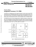
1
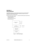
7.1 MODULE OVERVIEW
Features of the serial module are as follows:
• Two, Independent, Full-Duplex Asynchronous/Synchronous Receiver/Transmitter
Channels
SECTION 7
SERIAL MODULE
• Maximum Data Transfer Rate:
The MC68340 serial module is a dual universal asynchronous/synchronous
receiver/transmitter that interfaces directly to the CPU32 processor via the intermodule
bus (IMB). The serial module, shown in Figure 7-1, consists of the following major
functional areas:
• Quadruple-Buffered Receiver
—1× mode: 3 Mbps @ 8.39 MHz CLKOUT, 9.8 Mbps @25 MHz CLKOUT
—16× mode: 188 kbps @ 8.39 MHz CLKOUT, 612 kbps @25 MHz CLKOUT
• Two Independent Serial Communication Channels (A and B)
• Double-Buffered Transmitter
• Independently Programmable Baud Rate for Each Receiver and Transmitter
Selectable from:
—19 Fixed Rates: 50 to 76.8k Baud
• Baud Rate Generator Logic
—External 1× Clock or 16× Clock
• Internal Channel Control Logic
• Programmable Data Format:
• Interrupt Control Logic
—Five to Eight Data Bits Plus Parity
SERIAL COMMUNICATIONS
CHANNELS A AND B
BAUD RATE
GENERATOR LOGIC
CTSA
RTSA
RxDA
TxDA
RxRDYA
TxRDYA
CTSB
RTSB
RxDB
TxDB
—Odd, Even, No Parity, or Force Parity
—Nine-Sixteenths to Two Stop Bits Programmable in One-Sixteenth Bit Increments
• Programmable Channel Modes:
..... ..... .
—Normal (Full Duplex)
—Automatic Echo
—Local Loopback
—Remote Loopback
X1
X2
SCLK
• Automatic Wakeup Mode for Multidrop Applications
• Seven Maskable Interrupt Conditions
• Parity, Framing, and Overrun Error Detection
INTERNAL CHANNEL
CONTROL LOGIC
• False-Start Bit Detection
• Line-Break Detection and Generation
INTERRUPT CONTROL
LOGIC
• Detection of Breaks Originating in the Middle of a Character
• Start/End Break Interrupt/Status
• On-Chip Crystal Oscillator
Figure 7-1. Simplified Block Diagram
MOTOROLA
MC68340 USER’S MANUAL
7- 1
7- 2
MC68340 USER’S MANUAL
MOTOROLA
7.1.1 Serial Communication Channels A and B
Each communication channel provides a full-duplex asynchronous/synchronous receiver
and transmitter using an operating frequency independently selected from a baud rate
generator or an external clock input.
The transmitter accepts parallel data from the IMB, converts it to a serial bit stream,
inserts the appropriate start, stop, and optional parity bits, then outputs a composite serial
data stream on the channel transmitter serial data output (TxDx). Refer to 7.3.2.1
Transmitter for additional information.
The receiver accepts serial data on the channel receiver serial data input (RxDx), converts
it to parallel format, checks for a start bit, stop bit, parity (if any), or break condition, and
transfers the assembled character onto the IMB during read operations. Refer to 7.3.2.2
Receiver for additional information.
currently active interrupt conditions. The interrupt enable register (IER) is programmable
to mask any events that can cause an interrupt.
7.1.5 Comparison of Serial Module to MC68681
The serial module is code compatible with the MC68681 with some modifications. The
following paragraphs describe the differences.
The programming model is slightly altered. The supervisor/user block in the MC68340
closely follows the MC68681. The supervisor-only block has the following changes:
• The interrupt vector register is moved from supervisor/user to supervisor only at a
new address.
• MR2A and MR2B are moved from a hidden address location to a location at the
bottom of the programming model.
7.1.2 Baud Rate Generator Logic
The timer/counter is eliminated as well as all associated command and status registers.
The crystal oscillator operates directly from a 3.6864-MHz crystal connected across the
X1 input and the X2 output or from an external clock of the same frequency connected to
X1. The clock serves as the basic timing reference for the baud rate generator and other
internal circuits.
Only certain output port pins are available.
The baud rate generator operates from the oscillator or external TTL clock input and is
capable of generating 19 commonly used data communication baud rates ranging from 50
to 76.8k by producing internal clock outputs at 16 times the actual baud rate. Refer to 7.2
Serial Module Signal Definitions and 7.3.1 Baud Rate Generator for additional
information.
There are no IP pins on the MC68340.
RxRTS and TxRTS are more automated on the MC68340.
The XTAL_RDY bit in the ISR should be polled until it is cleared to prevent an unstable
frequency from being applied to the baud rate generator. The following code is an
example:
if (XTAL_RDY==0)
begin
write CSR
end
else
begin
wait
jump loop
end
The external clock input (SCLK), which bypasses the baud rate generator, provides a
synchronous clock mode of operation when used as a divide-by-1 clock and an
asynchronous clock mode when used as a divide-by-16 clock. The external clock input
allows the user to use SCLK as the only clock source for the serial module if multiple baud
rates are not required.
7.1.3 Internal Channel Control Logic
The serial module receives operation commands from the host and, in turn, issues
appropriate operation signals to the internal serial module control logic. This mechanism
allows the registers within the module to be accessed and various commands to be
performed. Refer to 7.4 Register Description and Programming for additional
information.
7.2 SERIAL MODULE SIGNAL DEFINITIONS
The following paragraphs contain a brief description of the serial module signals. Figure 72 shows both the external and internal signal groups.
NOTE
The terms assertion and negation are used throughout this
section to avoid confusion when dealing with a mixture of
active-low and active-high signals. The term assert or assertion
indicates that a signal is active or true, independent of the level
represented by a high or low voltage. The term negate or
negation indicates that a signal is inactive or false.
7.1.4 Interrupt Control Logic
Seven interrupt request (IRQ7–IRQ1) signals are provided to notify the CPU32 that an
interrupt has occurred. These interrupts are described in 7.4 Register Description and
Programming. The interrupt status register (ISR) is read by the CPU32 to determine all
MOTOROLA
MC68340 USER’S MANUAL
7- 3
7- 4
MC68340 USER’S MANUAL
MOTOROLA
7.2.3 External Input (SCLK)
ADDRESS BUS
IMB
INTERFACE
SIGNALS
X1
CONTROL
INTERNAL
CONTROL
LOGIC
S
DATA BUS
D15–D0
DATA
DATA BUS
MUX
BAUD RATE
GENERATOR
LOGIC
E
R
I
A
L
This input can be used as the clock input for channel A and/or channel B and is
programmable in the clock-select registers (CSR). When used as the receiver clock,
received data is sampled on the rising edge of the clock. When used as the transmitter
clock, data is output on the falling edge of the clock. If this input is not used, it must be
connected to VCC or GND.
X2
SCLK
7.2.4 Channel A Transmitter Serial Data Output (TxDA)
CHANNEL A
D7–D0
FOUR-CHARACTER
RECEIVE BUFFER
RxDA
TWO-CHARACTER
TRANSMIT BUFFER
TxDA
L
E
RTSA
I
N
T
E
R
N
A
L
B
U
S
CTSA
TxRDYA
This signal is the transmitter serial data output for channel A. The output is held high
('mark' condition) when the transmitter is disabled, idle, or operating in the local loopback
mode. Data is shifted out on this signal on the falling edge of the clock source, with the
least significant bit transmitted first.
EXTERNAL
INTERFACE SIGNALS
M
O
D
U
7.2.5 Channel A Receiver Serial Data Input (RxDA)
This signal is the receiver serial data input for channel A. Data received on this signal is
sampled on the rising edge of the clock source, with the least significant bit received first.
RxRDYA
..... ..... . ..
7.2.6 Channel B Transmitter Serial Data Output (TxDB)
CHANNEL B
FOUR-CHARACTER
RECEIVE BUFFER
TWO-CHARACTER
TRANSMIT BUFFER
This signal is the transmitter serial data output for channel B. The output is held high
('mark' condition) when the transmitter is disabled, idle, or operating in the local loopback
mode. Data is shifted out on this signal at the falling edge of the clock source, with the
least significant bit transmitted first.
RxDB
TxDB
7.2.7 Channel B Receiver Serial Data Input (RxDB)
RTSB
CTSB
This signal is the receiver serial data input for channel B. Data on this signal is sampled
on the rising edge of the clock source, with the least significant bit received first.
Figure 7-2. External and Internal Interface Signals
7.2.8 Channel A Request-To-Send ( RTSA)
7.2.1 Crystal Input or External Clock (X1)
This input is one of two connections to a crystal or a single connection to an external
clock. A crystal or an external clock signal, at 3.6864 MHz, must be supplied when using
the baud rate generator. If a crystal is used, a capacitor of approximately 10 pF should be
connected from this signal to ground. If this input is not used, it must be connected to VCC
or GND. Refer to Section 10 Applications for an example of a clock driver circuit.
7.2.2 Crystal Output (X2)
This output is the additional connection to a crystal. If a crystal is used, a capacitor of
approximately 5 pF should be connected from this signal to ground. If an external TTLlevel clock is used on X1, the X2 output must be left open. Refer to Section 10
Applications for an example of a clock driver circuit.
MOTOROLA
MC68340 USER’S MANUAL
7- 5
This active-low output signal is programmable as the channel A request-to-send or as a
dedicated parallel output.
7.2.8.1 RTSA . When used for this function, this signal can be programmed to be
automatically negated and asserted by either the receiver or transmitter. When connected
to the clear-to-send ( CTS≈) input of a transmitter, this signal can be used to control serial
data flow.
7.2.8.2 OP0. When used for this function, this output is controlled by bit 0 in the output
port data register (OP).
7.2.9 Channel B Request-To-Send ( RTSB)
This active-low output signal is programmable as the channel B request-to-send or as a
dedicated parallel output.
7- 6
MC68340 USER’S MANUAL
MOTOROLA
7.2.9.1 RTSB . When used for this function, this signal can be programmed to be
automatically negated and asserted by either the receiver or transmitter. When connected
to the CTS≈ input of a transmitter, this signal can be used to control serial data flow.
7.2.9.2 OP1. When used for this function, this output is controlled by bit 1 in the OP.
7.3 OPERATION
The following paragraphs describe the operation of the baud rate generator, transmitter
and receiver, and other functional operating modes of the serial module.
7.3.1 Baud Rate Generator
The baud rate generator consists of a crystal oscillator, baud rate generator, and clock
selectors (see Figure 7-3). The crystal oscillator operates directly from a 3.6864-MHz
crystal or from an external clock of the same frequency. The SCLK input bypasses the
baud rate generator and provides a synchronous clock mode of operation when used as a
divide-by-1 clock and an asynchronous clock mode when used as a divide-by-16 clock.
The clock is selected by programming the clock-select register (CSR) for each channel.
7.2.10 Channel A Clear-To-Send (CTSA)
This active-low input is the channel A clear-to-send.
7.2.11 Channel B Clear-To-Send (CTSB)
This active-low input is the channel B clear-to-send.
7.2.12 Channel A Transmitter Ready (T≈RDYA)
BAUD RATE
GENERATOR LOGIC
This active-low output signal is programmable as the channel A transmitter ready or as a
dedicated parallel output, and cannot be masked by the interrupt enable register (IER).
CRYSTAL
OSCILLATOR
7.2.12.1 T≈RDYA. When used for this function, this signal reflects the complement of the
status of bit 2 of the channel A status register (SRA). This signal can be used to control
parallel data flow by acting as an interrupt to indicate when the transmitter contains a
character.
EXTERNAL
INTERFACE
..... ..... . ... .
X1
BAUD RATE
GENERATOR
7.2.12.2 OP6. When used for this function, this output is controlled by bit 6 in the OP.
X2
SCLK
7.2.13 Channel A Receiver Ready ( R≈RDYA)
This active-low output signal is programmable as the channel A receiver ready, channel A
FIFO full indicator, or a dedicated parallel output, and cannot be masked by the IER.
CLOCK
SELECTORS
7.2.13.1 R≈RDYA. When used for this function, this signal reflects the complement of the
status of bit 1 of the ISR. This signal can be used to control parallel data flow by acting as
an interrupt to indicate when the receiver contains a character.
7.2.13.2 FFULLA. When used for this function, this signal reflects the complement of the
status of bit 1 of the ISR. This signal can be used to control parallel data flow by acting as
an interrupt to indicate when the receiver FIFO is full.
7.2.13.3 OP4. When used for this function, this output is controlled by bit 4 in the OP.
MOTOROLA
MC68340 USER’S MANUAL
7- 7
Figure 7-3. Baud Rate Generator Block Diagram
7.3.2 Transmitter and Receiver Operating Modes
The functional block diagram of the transmitter and receiver, including command and
operating registers, is shown in Figure 7-4. The paragraphs that follow contain
descriptions for both these functions in reference to this diagram. For detailed register
information, refer to 7.4 Register Description and Programming.
7- 8
MC68340 USER’S MANUAL
MOTOROLA
CHANNEL A
COMMAND REGISTER (CRA)
W
MODE REGISTER A (MR1A)
R/W
MODE REGISTER B (MR2A)
R/W
STATUS REGISTER (SRA)
TRANSMIT
BUFFER (TBA)
(2 REGISTERS)
7.3.2.1 TRANSMITTER. The transmitters are enabled through their respective command
registers (CR) located within the serial module. The serial module signals the CPU32
when it is ready to accept a character by setting the transmitter-ready bit (TxRDY) in the
channel's status register (SR). Functional timing information for the transmitter is shown in
Figure 7-5.
EXTERNAL
INTERFACE
The transmitter converts parallel data from the CPU32 to a serial bit stream on TxDx. It
automatically sends a start bit followed by the programmed number of data bits, an
optional parity bit, and the programmed number of stop bits. The least significant bit is
sent first. Data is shifted from the transmitter output on the falling edge of the clock
source.
R
TRANSMIT HOLDING REGISTER
W
TxDA
C1 IN
TRANSMISSION
TRANSMIT SHIFT REGISTER
RECEIVER HOLDING REGISTER 1
FIFO
R
TxDx
C1
C2
C3
C4
BREAK
C6
RECEIVER HOLDING REGISTER 2
RECEIVE
BUFFER (RBA)
(4 REGISTERS)
RECEIVER HOLDING REGISTER 3
RxDA
RECEIVER SHIFT REGISTER
TRANSMITTER
ENABLED
TxRDY
(SR2)
CHANNEL B
COMMAND REGISTER (CRB)
W
CS
MODE REGISTER 1 (MR1B)
R/W
MODE REGISTER 2 (MR2B)
R/W
W
W
W
W
W
W
W
W
C1
C2
C3
START
BREAK
C4
STOP
BREAK
C5
NOT
TRANSMITTED
C6
1
CTS
TRANSMIT
BUFFER (TBB)
(2 REGISTERS)
STATUS REGISTER (SRB)
R
TRANSMIT HOLDING REGISTER
W
RTS 2
R
NOTES:
1. TIMING SHOWN FOR MR2(4) = 1
2. TIMING SHOWN FOR MR2(5) = 1
3. C N = TRANSMIT CHARACTER
4. W = WRITE
FIFO
RECEIVER HOLDING REGISTER 2
RECEIVER HOLDING REGISTER 3
RECEIVER SHIFT REGISTER
RxDB
Figure 7-5. Transmitter Timing Diagram
Following transmission of the stop bits, if a new character is not available in the transmitter
holding register, the TxDx output remains high ('mark' condition), and the transmitter
empty bit (TxEMP) in the SR is set. Transmission resumes and the TxEMP bit is cleared
when the CPU32 loads a new character into the transmitter buffer (TB). If a disable
command is sent to the transmitter, it continues operating until the character in the
NOTE:
R/W = READ/WRITE
R = READ
W = WRITE
..... ..... . ... . . .
Figure 7-4. Transmitter and Receiver Functional Diagram
MOTOROLA
MANUALLY
ASSERTED
TRANSMIT SHIFT REGISTER
RECEIVER HOLDING REGISTER 1
RECEIVE
BUFFER (RBB)
(4 REGISTERS)
MANUALLY ASSERTED
BY BIT- SET COMMAND
TxDB
MC68340 USER’S MANUAL
7- 9
7- 10
MC68340 USER’S MANUAL
MOTOROLA
transmit shift register, if any, is completely sent out. If the transmitter is reset through a
software command, operation ceases immediately (refer to 7.4.1.7 Command Register
(CR)). The transmitter is re-enabled through the CR to resume operation after a disable or
software reset.
If clear-to-send operation is enabled, CTS≈ must be asserted for the character to be
transmitted. If CTS≈ is negated in the middle of a transmission, the character in the shift
register is transmitted, and TxDx remains in the 'mark' state until CTS≈ is asserted again.
If the transmitter is forced to send a continuous low condition by issuing a send break
command, the state of CTS≈ is ignored by the transmitter.
The transmitter can be programmed to automatically negate request-to-send (RTS≈)
outputs upon completion of a message transmission. If the transmitter is programmed to
operate in this mode, RTS≈ must be manually asserted before a message is transmitted.
In applications in which the transmitter is disabled after transmission is complete and
RTS≈ is appropriately programmed, RTS≈ is negated one bit time after the character in
the shift register is completely transmitted. The transmitter must be manually re-enabled
by reasserting RTS≈ before the next message is to be sent.
RxD
C2
C1
C3
C4
C5
C6
C8
C7
C6, C7, C8 ARE LOST
RECEIVER
ENABLED
RxRDY
(SR0)
FFULL
(SR1)
RxRDYA
CS
7.3.2.2 RECEIVER. The receivers are enabled through their respective CRs located within
the serial module. Functional timing information for the receiver is shown in Figure 7-6.
The receiver looks for a high-to-low (mark-to-space) transition of the start bit on RxDx.
When a transition is detected, the state of RxDx is sampled each 16× clock for eight
clocks, starting one-half clock after the transition (asynchronous operation) or at the next
rising edge of the bit time clock (synchronous operation). If RxDx is sampled high, the
start bit is invalid, and the search for the valid start bit begins again. If RxDx is still low, a
valid start bit is assumed, and the receiver continues to sample the input at one-bit time
intervals, at the theoretical center of the bit, until the proper number of data bits and parity,
if any, is assembled and one stop bit is detected. Data on the RxDx input is sampled on
the rising edge of the programmed clock source. The least significant bit is received first.
The data is then transferred to a receiver holding register, and the RxRDY bit in the
appropriate SR is set. If the character length is less than eight bits, the most significant
unused bits in the receiver holding register are cleared.
After the stop bit is detected, the receiver immediately looks for the next start bit.
However, if a nonzero character is received without a stop bit (framing error) and RxDx
remains low for one-half of the bit period after the stop bit is sampled, the receiver
operates as if a new start bit is detected. The parity error (PE), framing error (FE), overrun
error (OE), and received break (RB) conditions (if any) set error and break flags in the
appropriate SR at the received character boundary and are valid only when the RxRDY bit
in the SR is set.
If a break condition is detected (RxDx is low for the entire character including the stop bit),
a character of all zeros is loaded into the receiver holding register, and the RB and
RxRDY bits in the SR are set. The RxDx signal must return to a high condition for at least
one-half bit time before a search for the next start bit begins.
MOTOROLA
MC68340 USER’S MANUAL
7- 11
R
R
R R
R R R R
STATUS DATA STATUS DATA STATUS DATA
STATUS DATA
C1
C2
C3
C4
C5
LOST
OVERRUN
(SR4)
1
RTS
RESET BY COMMAND
OPR(0) = 1
NOTES:
1. Timing shown for MR1(7) = 1
2. Timing shown for OPCR(4) = 1 and MR1(6) = 0
3. R = Read
4. CN = Received Character
Figure 7-6. Receiver Timing Diagram
The receiver detects the beginning of a break in the middle of a character if the break
persists through the next character time. When the break begins in the middle of a
character, the receiver places the damaged character in the receiver first-in-first-out
(FIFO) stack and sets the corresponding error conditions and RxRDY bit in the SR. Then,
if the break persists until the next character time, the receiver places an all-zero character
into the receiver FIFO and sets the corresponding RB and RxRDY bits in the SR.
7.3.2.3 FIFO STACK. The FIFO stack is used in each channel's receiver buffer logic. The
stack consists of three receiver holding registers. The receive buffer consists of the FIFO
and a receiver shift register connected to the RxDx (refer to Figure 7-4). Data is
7- 12
MC68340 USER’S MANUAL
MOTOROLA
assembled in the receiver shift register and loaded into the top empty receiver holding
register position of the FIFO. Thus, data flowing from the receiver to the CPU32 is
quadruple buffered.
In addition to the data byte, three status bits, PE, FE, and RB, are appended to each data
character in the FIFO; OE is not appended. By programming the ERR bit in the channel's
mode register (MR1), status is provided in character or block modes.
The RxRDY bit in the SR is set whenever one or more characters are available to be read
by the CPU32. A read of the receiver buffer produces an output of data from the top of the
FIFO stack. After the read cycle, the data at the top of the FIFO stack and its associated
status bits are 'popped', and new data can be added at the bottom of the stack by the
receiver shift register. The FIFO-full status bit (FFULL) is set if all three stack positions are
filled with data. Either the RxRDY or FFULL bit can be selected to cause an interrupt.
In the character mode, status provided in the SR is given on a character-by-character
basis and thus applies only to the character at the top of the FIFO. In the block mode, the
status provided in the SR is the logical OR of all characters coming to the top of the FIFO
stack since the last reset error command. A continuous logical OR function of the
corresponding status bits is produced in the SR as each character reaches the top of the
FIFO stack. The block mode is useful in applications where the software overhead of
checking each character's error cannot be tolerated. In this mode, entire messages are
received, and only one data integrity check is performed at the end of the message. This
mode allows a data-reception speed advantage, but does have a disadvantage since
each character is not individually checked for error conditions by software. If an error
occurs within the message, the error is not recognized until the final check is performed,
and no indication exists as to which character in the message is at fault.
In either mode, reading the SR does not affect the FIFO. The FIFO is 'popped' only when
the receive buffer is read. The SR should be read prior to reading the receive buffer. If all
three of the FIFO's receiver holding registers are full when a new character is received,
the new character is held in the receiver shift register until a FIFO position is available. If
an additional character is received during this state, the contents of the FIFO are not
affected. However, the character previously in the receiver shift register is lost, and the OE
bit in the SR is set when the receiver detects the start bit of the new overrunning
character.
To support control flow capability, the receiver can be programmed to automatically
negate and assert RTS≈ . When in this mode, RTS≈ is automatically negated by the
receiver when a valid start bit is detected and the FIFO stack is full. When a FIFO position
becomes available, RTS≈ is asserted by the receiver. Using this mode of operation,
overrun errors are prevented by connecting the R T S ≈ to the CTS≈ input of the
transmitting device.
7.3.3 Looping Modes
Each serial module channel can be configured to operate in various looping modes as
shown in Figure 7-7. These modes are useful for local and remote system diagnostic
functions. The modes are described in the following paragraphs with further information
available in 7.4 Register Description and Programming.
The channel's transmitter and receiver should both be disabled when switching between
modes. The selected mode is activated immediately upon mode selection, regardless of
whether a character is being received or transmitted.
7.3.3.1 AUTOMATIC ECHO MODE. In this mode, the channel automatically retransmits
the received data on a bit-by-bit basis. The local CPU32-to-receiver communication
continues normally, but the CPU32-to-transmitter link is disabled. While in this mode,
received data is clocked on the receiver clock and retransmitted on TxDx. The receiver
must be enabled, but the transmitter need not be enabled.
Since the transmitter is not active, the SR TxEMP and TxRDY bits are inactive, and data
is transmitted as it is received. Received parity is checked, but not recalculated for
transmission. Character framing is also checked, but stop bits are transmitted as received.
A received break is echoed as received until the next valid start bit is detected.
7.3.3.2 LOCAL LOOPBACK MODE. In this mode, TxDx is internally connected to RxDx.
This mode is useful for testing the operation of a local serial module channel by sending
data to the transmitter and checking data assembled by the receiver. In this manner,
correct channel operations can be assured. Also, both transmitter and CPU32-to-receiver
communications continue normally in this mode. While in this mode, the RxDx input data
is ignored, the TxDx is held marking, and the receiver is clocked by the transmitter clock.
The transmitter must be enabled, but the receiver need not be enabled.
7.3.3.3 REMOTE LOOPBACK MODE. In this mode, the channel automatically transmits
received data on the TxDx output on a bit-by-bit basis. The local CPU32-to-transmitter link
is disabled. This mode is useful in testing receiver and transmitter operation of a remote
channel. While in this mode, the receiver clock is used for the transmitter.
Since the receiver is not active, received data cannot be read by the CPU32, and the error
status conditions are inactive. Received parity is not checked and is not recalculated for
transmission. Stop bits are transmitted as received. A received break is echoed as
received until the next valid start bit is detected.
If the FIFO stack contains characters and the receiver is disabled, the characters in the
FIFO can still be read by the CPU32. If the receiver is reset, the FIFO stack and all
receiver status bits, corresponding output ports, and interrupt request are reset. No
additional characters are received until the receiver is re-enabled.
MOTOROLA
MC68340 USER’S MANUAL
7- 13
7- 14
MC68340 USER’S MANUAL
MOTOROLA
RxDx
INPUT
Rx
RxD
C2
C1
C3
C4
C5
C6
C8
C7
CPU
DISABLED
Tx
C6, C7, C8 ARE LOST
DISABLED
TxDx
OUTPUT
RECEIVER
ENABLED
(a) Automatic Echo
RxRDY
(SR0)
DISABLED
Rx
RxDx
INPUT
FFULL
(SR1)
CPU
DISABLED
Tx
TxDx
OUTPUT
RxRDYA
(b) Local Loopback
CS
DISABLED
Rx
DISABLED
R
RxDx
INPUT
R
R R
R R R R
STATUS DATA STATUS DATA STATUS DATA
STATUS DATA
C1
CPU
DISABLED
Tx
DISABLED
TxDx
OUTPUT
C2
C3
C4
C5
LOST
OVERRUN
(SR4)
(c) Remote Loopback
1
RTS
RESET BY COMMAND
Figure 7-7. Looping Modes Functional Diagram
OPR(0) = 1
7.3.4 Multidrop Mode
A channel can be programmed to operate in a wakeup mode for multidrop or
multiprocessor applications. Functional timing information for the multidrop mode is shown
in Figure 7-8. The mode is selected by setting bits 3 and 4 in mode register 1 (MR1). This
mode of operation allows the master station to be connected to several slave stations
(maximum of 256). In this mode, the master transmits an address character followed by a
block of data characters targeted for one of the slave stations. The slave stations have
their channel receivers disabled. However, they continuously monitor the data stream sent
out by the master station. When an address character is sent by the master, the slave
receiver channel notifies its respective CPU by setting the RxRDY bit in the SR and
generating an interrupt (if programmed to do so). Each slave station CPU then compares
the received address to its station address and enables its receiver if it wishes to receive
the subsequent data characters or block of data from the master station. Slave stations
not addressed continue to monitor the data stream for the next address character. Data
fields in the data stream are separated by an address character. After a slave receives a
block of data, the slave station's CPU disables the receiver and initiates the process
again.
MOTOROLA
MC68340 USER’S MANUAL
7- 15
NOTES:
1. Timing shown for MR1(7) = 1
2. Timing shown for OPCR(4) = 1 and MR1(6) = 0
3. R = Read
4. CN = Received Character
Figure 7-8. Multidrop Mode Timing Diagram
A transmitted character from the master station consists of a start bit, a programmed
number of data bits, an address/data (A/D) bit flag, and a programmed number of stop
bits. The A/D bit identifies the type of character being transmitted to the slave station. The
character is interpreted as an address character if the A/D bit is set or as a data character
if the A/D bit is cleared. The polarity of the A/D bit is selected by programming bit 2 of the
MR1. The MR1 should be programmed before enabling the transmitter and loading the
corresponding data bits into the transmit buffer.
In multidrop mode, the receiver continuously monitors the received data stream,
regardless of whether it is enabled or disabled. If the receiver is disabled, it sets the
7- 16
MC68340 USER’S MANUAL
MOTOROLA
RxRDY bit and loads the character into the receiver holding register FIFO stack provided
the received A/D bit is a one (address tag). The character is discarded if the received A/D
bit is a zero (data tag). If the receiver is enabled, all received characters are transferred to
the CPU32 via the receiver holding register stack during read operations.
In either case, the data bits are loaded into the data portion of the stack while the A/D bit
is loaded into the status portion of the stack normally used for a parity error (SR bit 5).
Framing error, overrun error, and break detection operate normally. The A/D bit takes the
place of the parity bit; therefore, parity is neither calculated nor checked. Messages in this
mode may still contain error detection and correction information. One way to provide
error detection, if 8-bit characters are not required, is to use software to calculate parity
and append it to the 5-, 6-, or 7-bit character.
7.3.5 Bus Operation
This section describes the operation of the IMB during read, write, and interrupt
acknowledge cycles to the serial module. All serial module registers must be accessed as
bytes.
NOTE
All serial module registers are only accessible as bytes. The
contents of the mode registers (MR1 and MR2), clock-select
register (CSR), and the auxiliary control register (ACR) bit 7
should only be changed after the receiver/transmitter is issued
a software RESET command—i.e., channel operation must be
disabled. Care should also be taken if the register contents are
changed during receiver/transmitter operations, as undesirable
results may be produced.
In the registers discussed in the following pages, the numbers in the upper right-hand
corner indicate the offset of the register from the base address specified in the module
base address register (MBAR) in the SIM40. The numbers above the register description
represent the bit position in the register. The register description contains the mnemonic
for the bit. The values shown below the register description are the values of those
register bits after a hardware reset. A value of U indicates that the bit value is unaffected
by reset. The read/write status and the access privilege are shown in the last line.
NOTE
7.3.5.1 READ CYCLES. The serial module is accessed by the CPU32 with no wait states.
The serial module responds to byte reads. Reserved registers return logic zero during
reads.
A CPU32 RESET instruction will not affect the MCR, but will
reset all the other serial module registers as though a
hardware reset had occurred. The module is enabled when the
STP bit in the MCR is cleared. The module is disabled when
the STP bit in the MCR is set.
7.3.5.2 WRITE CYCLES. The serial module is accessed by the CPU32 with no wait
states. The serial module responds to byte writes. Write cycles to read-only registers and
reserved registers complete in a normal manner without exception processing; however,
the data is ignored.
7.3.5.3 INTERRUPT ACKNOWLEDGE CYCLES. The serial module is capable of
arbitrating for interrupt servicing and supplying the interrupt vector when it has
successfully won arbitration. The vector number must be provided if interrupt servicing is
necessary; thus, the interrupt vector register (IVR) must be initialized. If the IVR is not
initialized, a spurious interrupt exception will be taken if interrupts are generated.
7.4 REGISTER DESCRIPTION AND PROGRAMMING
This section contains a detailed description of each register and its specific function as
well as flowcharts of basic serial module programming.
7.4.1 Register Description
The operation of the serial module is controlled by writing control bytes into the
appropriate registers. A list of serial module registers and their associated addresses are
shown in Figure 7-9. The mode, status, command, and clock-select registers are
duplicated for each channel to provide independent operation and control.
MOTOROLA
MC68340 USER’S MANUAL
7- 17
7- 18
MC68340 USER’S MANUAL
MOTOROLA
Address
FC
S1
Register Read (R/W = 1)
Register Write (R/W = 0)
700
MCR (HIGH BYTE)
MCR (HIGH BYTE)
701
S
702
S
703
S
MCR (LOW BYTE)
DO NOT ACCESS3
DO NOT ACCESS3
MCR (LOW BYTE)
DO NOT ACCESS3
DO NOT ACCESS3
704
S
INTERRUPT LEVEL (ILR)
NTERRUPT LEVEL (ILR)
705
S
INTERRUPT VECTOR (IVR)
INTERRUPT VECTOR (IVR)
710
S/U2
MODE REGISTER 1A (MR1A)
MODE REGISTER 1A (MR1A)
711
S/U
CLOCK-SELECT REGISTER A (CSRA)
712
S/U
STATUS REGISTER A (SRA)
DO NOT ACCESS3
713
S/U
RECEIVER BUFFER A (RBA)
TRANSMITTER BUFFER A (TBA)
714
S/U
INPUT PORT CHANGE REGISTER (IPCR)
AUXILIARY CONTROL REGISTER (ACR)
715
S/U
716
S/U
INTERRUPT STATUS REGISTER (ISR)
DO NOT ACCESS3
INTERRUPT ENABLE REGISTER (IER)
DO NOT ACCESS3
717
S/U
DO NOT ACCESS3
DO NOT ACCESS3
718
S/U
MODE REGISTER 1B (MR1B)
MODE REGISTER 1B (MR1B)
719
S/U
S/U
STATUS REGISTER B (SRB)
DO NOT ACCESS3
CLOCK-SELECT REGISTER B (CSRB)
71A
71B
S/U
RECEIVER BUFFER B (RBB)
TRANSMITTER BUFFER B (TBB)
STP—Stop Mode Bit
1 = The serial module will be disabled. Setting the STP bit stops all clocks within the
serial module (including the crystal or external clock and SCLK), except for the
clock from the IMB. The clock from the IMB remains active to allow CPU32
access to the MCR. The clock stops on the low phase of the clock and remains
stopped until the STP bit is cleared by the CPU32 or a hardware reset. Accesses
to serial module registers while in stop mode produce a bus error. The serial
module should be disabled in a known state prior to setting the STP bit;
otherwise, unpredictable results may occur. The STP bit should be set prior to
executing the LPSTOP instruction to reduce overall power consumption.
0 = The serial module is enabled and will operate in normal mode. When STP = 0,
make sure the external crystal is stable (XTAL_RDY bit (bit 3) of the interrupt
status register (ISR) is zero) before continuing.
COMMAND REGISTER A (CRA)
NOTE
The serial module should be disabled (i.e., the STP bit in the
MCR is set) before executing the LPSTOP instruction to obtain
the lowest power consumption. The X1/X2 oscillator will
continue to run during LPSTOP if STP = 0.
COMMAND REGISTER B (CRB)
71C
S/U
DO NOT ACCESS3
DO NOT ACCESS3
71D
S/U
INPUT PORT REGISTER (IP)
DO NOT ACCESS3
OUTPUT PORT CONTROL REGISTER (OPCR)
OUTPUT PORT (OP)4 BIT SET
71E
S/U
71F
S/U
DO NOT ACCESS3
OUTPUT PORT (OP)4 BIT RESET
720
S/U
MODE REGISTER 2A (MR2A)
MODE REGISTER 2A (MR2A)
721
S/U
MODE REGISTER 2B (MR2B)
MODE REGISTER 2B (MR2B)
FRZ1–FRZ0—Freeze
These bits determine the action taken when the FREEZE signal is asserted on the IMB
when the CPU32 has entered background debug mode. Table 7-1 lists the action taken
for each combination of bits.
Table 7-1. FRZx Control Bits
NOTES:
1. S = Register permanently defined as supervisor-only access
2. S/U = Register programmable as either supervisor or user access
3. A read or write to these locations currently has no effect.
4. Address-triggered commands
Figure 7-9. Serial Module Programming Model
7.4.1.1 MODULE CONFIGURATION REGISTER (MCR). The MCR controls the serial
module configuration. This register can be either read or written when the module is
enabled and is in the supervisor state. The MCR is not affected by a CPU32 RESET
instruction. Only the MCR can be accessed when the module is disabled (i.e., the STP bit
in the MCR is set).
MCR
$700
15
14
13
12
11
10
9
8
7
6
5
4
STP
FRZ1
FRZ0
ICCS
0
0
0
0
SUPV
0
0
0
RESET:
0
0
0
0
0
0
0
0
1
0
0
0
Read/Write
MOTOROLA
3
2
1
0
0
0
IARB
0
0
FRZ1
FRZ0
0
0
Ignore FREEZE
Action
0
1
Reserved (FREEZE Ignored)
1
0
Freeze on Character Boundary
1
1
Freeze on Character Boundary
If FREEZE is asserted, channel A and channel B freeze independently of each other.
The transmitter and receiver freeze at character boundaries. The transmitter does not
freeze in the send break mode. Communications can be lost if the channel is not
programmed to support flow control. See Section 5 CPU32 for more information on
FREEZE.
ICCS—Input Capture Clock Select
1 = Selects SCLK as the clear-to-send input capture clock for both channels. Clearto-send operation is enabled by setting bit 4 in MR2. The data is captured on the
CTS≈ pins on the rising edge of the clock.
0 = The crystal clock is the clear-to-send input capture clock for both channels.
Supervisor Only
MC68340 USER’S MANUAL
7- 19
7- 20
MC68340 USER’S MANUAL
MOTOROLA
Bits 11–8, 6–4—Reserved
IVR
SUPV—Supervisor/User
The value of this bit has no affect on registers permanently defined as supervisor only.
1 = The serial module registers, which are defined as supervisor or user, reside in
supervisor data space and are only accessible from supervisor programs.
0 = The serial module registers, which are defined as supervisor or user, reside in
user data space and are accessible from either supervisor or user programs.
IARB3–IARB0—Interrupt Arbitration Bits
Each module that generates interrupts has an IARB field. These bits are used to
arbitrate for the bus in the case that two or more modules simultaneously generate an
interrupt at the same priority level. No two modules can share the same IARB value.
The reset value of the IARB field is $0, which prevents this module from arbitrating
during the interrupt acknowledge cycle. The system software should initialize the IARB
field to a value from $F (highest priority) to $1 (lowest priority).
6
5
4
3
2
1
0
0
0
0
0
0
IL2
IL1
IL0
RESET:
0
0
0
0
0
0
0
0
Read/Write
5
4
3
2
1
0
IVR7
IVR6
IVR5
IVR4
IVR3
IVR2
IVR1
IVR0
RESET:
0
0
0
0
1
1
1
1
7.4.1.4 MODE REGISTER 1 (MR1). MR1 controls some of the serial module
configuration. This register can be read or written at any time when the serial module is
enabled (i.e., the STP bit in the MCR is cleared).
MR1A, MR1B
Bits 7–3—Reserved
IL2–IL0—Interrupt Level Bits
Each module that can generate interrupts has an interrupt level field. The priority level
encoded in these bits is sent to the CPU32 on the appropriate IRQ≈ signal. The CPU32
uses this value to determine servicing priority. The hardware reset value of $00 will not
generate any interrupts. See Section 5 CPU32 for more information.
$710, $718
7
6
5
4
3
2
1
0
RxRTS
R/F
ERR
PM1
PM0
PT
B/C1
B/C0
RESET:
0
0
0
0
0
0
0
0
Read/Write
Supervisor Only
Supervisor Only
IVR7–IVR0—Interrupt Vector Bits
Each module that generates interrupts has an interrupt vector field. This 8-bit number
indicates the offset from the base of the vector table where the address of the exception
handler for the specified interrupt is located. The IVR is reset to $0F, which indicates an
uninitialized interrupt condition. See Section 5 CPU32 for more information.
$704
7
6
Read /Write
7.4.1.2 INTERRUPT LEVEL REGISTER (ILR). The ILR contains the priority level for the
serial module interrupt request. When the serial module is enabled (i.e., the STP bit in the
MCR is cleared), this register can be read or written to at any time while in supervisor
mode.
ILR
$705
7
Supervisor/User
RxRTS—Receiver Request-to-Send Control
1 = Upon receipt of a valid start bit, RTS≈ is negated if the channel's FIFO is full.
RTS≈ is reasserted when the FIFO has an empty position available.
0 = RTS≈ is asserted by setting bit 1 or 0 in the OP and negated by clearing bit 1 or
0 in the OP.
This feature can be used for flow control to prevent overrun in the receiver by using the
RTS≈ output to control the CTS≈ input of the transmitting device. If both the receiver
and transmitter are programmed for RTS control, RTS control will be disabled for both
since this configuration is incorrect. See 7.4.1.17 Mode Register 2 for information on
programming the transmitter RTS≈ control.
7.4.1.3 INTERRUPT VECTOR REGISTER (IVR). The IVR contains the 8-bit vector
number of the interrupt. When the serial module is enabled (i.e., the STP bit in the MCR is
cleared), this register can be read or written to at any time while in supervisor mode.
R/F—Receiver-Ready Select
1 = Bit 5 for channel B and bit 1 for channel A in the ISR reflect the channel FIFO full
status. These ISR bits are set when the receiver FIFO is full and are cleared
when a position is available in the FIFO.
0 = Bit 5 for channel B and bit 1 for channel A in the ISR reflect the channel receiverready status. These ISR bits are set when a character has been received and are
cleared when the CPU32 reads the receive buffer.
MOTOROLA
7- 22
MC68340 USER’S MANUAL
7- 21
MC68340 USER’S MANUAL
MOTOROLA
ERR—Error Mode
This bit controls the meaning of the three FIFO status bits (RB, FE, and PE) in the SR
for the channel.
1 = Block mode—The values in the channel SR are the accumulation (i.e., the logical
OR) of the status for all characters coming to the top of the FIFO since the last
reset error status command for the channel was issued. Refer to 7.4.1.7
Command Register (CR) for more information on serial module commands.
0 = Character mode—The values in the channel SR reflect the status of the
character at the top of the FIFO.
NOTE
ERR = 0 must be used to get the correct A/D flag information
when in multidrop mode.
Table 7-3. B/Cx Control Bits
Table 7-2. PMx and PT Control Bits
Parity Mode
PT
Parity Type
0
0
With Parity
0
Even Parity
0
0
With Parity
1
Odd Parity
0
1
Force Parity
0
Low Parity
0
1
Force Parity
1
High Parity
1
0
No Parity
X
No Parity
1
1
Multidrop Mode
0
Data Character
1
1
Multidrop Mode
1
Address Character
Bits/Character
0
Five Bits
0
1
Six Bits
1
0
Seven Bits
1
1
Eight Bits
SRA, SRB
PT—Parity Type
This bit selects the parity type if parity is programmed by the parity mode bits, and if
multidrop mode is selected, it configures the transmitter for data character transmission
or address character transmission. Table 7-2 lists the parity mode and type or the
multidrop mode for each combination of the parity mode and the parity type bits.
PM0
B/C0
0
7.4.1.5 STATUS REGISTER (SR). The SR indicates the status of the characters in the
FIFO and the status of the channel transmitter and receiver. This register can only be read
when the serial module is enabled (i.e., the STP bit in the MCR is cleared).
PM1–PM0—Parity Mode
These bits encode the type of parity used for the channel (see Table 7-2). The parity bit
is added to the transmitted character, and the receiver performs a parity check on
incoming data. These bits can alternatively select multidrop mode for the channel.
PM1
B/C1
$711, $719
7
6
5
4
3
2
1
0
RB
FE
PE
OE
TxEMP
TxRDY
FFULL
RxRDY
RESET:
0
0
0
0
0
0
0
0
Read Only
Supervisor/User
RB—Received Break
1 = An all-zero character of the programmed length has been received without a stop
bit. The RB bit is only valid when the RxRDY bit is set. Only a single FIFO
position is occupied when a break is received. Further entries to the FIFO are
inhibited until the channel RxDx returns to the high state for at least one-half bit
time, which is equal to two successive edges of the internal or external 1× clock
or 16 successive edges of the external 16× clock.
The received break circuit detects breaks that originate in the middle of a
received character. However, if a break begins in the middle of a character, it
must persist until the end of the next detected character time.
0 = No break has been received.
FE—Framing Error
1 = A stop bit was not detected when the corresponding data character in the FIFO
was received. The stop-bit check is made in the middle of the first stop-bit
position. The bit is valid only when the RxRDY bit is set.
0 = No framing error has occurred.
B/C1–B/C0—Bits per Character
These bits select the number of data bits per character to be transmitted. The character
length listed in Table 7-3 does not include start, parity, or stop bits.
PE—Parity Error
1 = When the with parity or force parity mode is programmed in the MR1, the
corresponding character in the FIFO was received with incorrect parity. When the
multidrop mode is programmed, this bit stores the received A/D bit. This bit is
valid only when the RxRDY bit is set.
0 = No parity error has occurred.
MOTOROLA
7- 24
MC68340 USER’S MANUAL
7- 23
MC68340 USER’S MANUAL
MOTOROLA
OE—Overrun Error
1 = One or more characters in the received data stream have been lost. This bit is
set upon receipt of a new character when the FIFO is full and a character is
already in the shift register waiting for an empty FIFO position. When this occurs,
the character in the receiver shift register and its break detect, framing error
status, and parity error, if any, are lost. This bit is cleared by the reset error status
command in the CR.
0 = No overrun has occurred.
TxEMP—Transmitter Empty
1 = The channel transmitter has underrun (both the transmitter holding register and
transmitter shift registers are empty). This bit is set after transmission of the last
stop bit of a character if there are no characters in the transmitter holding register
awaiting transmission.
0 = The transmitter buffer is not empty. The transmitter holding register is loaded by
the CPU32, or the transmitter is disabled. The transmitter is enabled/disabled by
programming the TCx bits in the CR.
TxRDY—Transmitter Ready
This bit is duplicated in the ISR; bit 0 for channel A and bit 4 for channel B.
1 = The transmitter holding register is empty and ready to be loaded with a character.
This bit is set when the character is transferred to the transmitter shift register.
This bit is also set when the transmitter is first enabled. Characters loaded into
the transmitter holding register while the transmitter is disabled are not
transmitted and are lost.
0 = The transmitter holding register was loaded by the CPU32, or the transmitter is
disabled.
7.4.1.6 CLOCK-SELECT REGISTER (CSR). The CSR selects the baud rate clock for the
channel receiver and transmitter. This register can only be written when the serial module
is enabled (i.e., the STP bit in the MCR is cleared).
NOTE
This register should only be written after the external crystal is
stable (XTAL_RDY bit of the ISR is zero).
CSRA, CSRB
7- 25
5
4
3
2
1
0
RCS3
RCS2
RCS1
RCS0
TCS3
TCS2
TCS1
TCS0
RESET:
0
0
0
0
0
0
0
0
Supervisor/User
RCS3–RCS0—Receiver Clock Select
These bits select the baud rate clock for the channel receiver from a set of baud rates
listed in Table 7-4. The baud rate set selected depends upon the auxiliary control
register (ACR) bit 7. Set 1 is selected if ACR bit 7 = 0, and set 2 is selected if ACR bit
7 = 1. The receiver clock is always 16 times the baud rate shown in this list, except
when SCLK is used.
Table 7-4. RCSx Control Bits
RxRDY—Receiver Ready
1 = A character has been received and is waiting in the FIFO to be read by the
CPU32. This bit is set when a character is transferred from the receiver shift
register to the FIFO.
0 = The CPU32 has read the receiver buffer, and no characters remain in the FIFO
after this read.
MC68340 USER’S MANUAL
6
Write Only
FFULL—FIFO Full
1 = A character was transferred from the receiver shift register to the receiver FIFO
and the transfer caused the FIFO to become full (all three FIFO holding register
positions are occupied).
0 = The CPU32 has read the receiver buffer and one or more FIFO positions are
available. Note that if there is a character in the receiver shift register because
the FIFO is full, this character will be moved into the FIFO when a position is
available, and the FIFO will remain full.
MOTOROLA
$711, $719
7
7- 26
RCS3
RCS2
RCS1
RCS0
Set 1
0
0
0
0
50
Set 2
75
0
0
0
1
110
110
0
0
1
0
134.5
134.5
0
0
1
1
200
150
0
1
0
0
300
300
0
1
0
1
600
600
0
1
1
0
1200
1200
0
1
1
1
1050
2000
1
0
0
0
2400
2400
1
0
0
1
4800
4800
1
0
1
0
7200
1800
1
0
1
1
9600
9600
1
1
0
0
38.4k
19.2k
1
1
0
1
76.8k
38.4k
1
1
1
0
SCLK/16
SCLK/16
1
1
1
1
SCLK/1
SCLK/1
MC68340 USER’S MANUAL
MOTOROLA
TCS3–TCS0—Transmitter Clock Select
These bits select the baud rate clock for the channel transmitter from a set of baud rates
listed in Table 7-5. The baud rate set selected depends upon ACR bit 7. Set 1 is
selected if ACR bit 7 = 0, and set 2 is selected if ACR bit 7 = 1. The transmitter clock is
always 16 times the baud rate shown in this list, except when SCLK is used.
MISC3–MISC0—Miscellaneous Commands
These bits select a single command as listed in Table 7-6.
Table 7-6. MISCx Control Bits
Table 7-5. TCSx Control Bits
TCS3
TCS2
TCS1
TCS0
0
0
0
0
0
0
0
1
0
0
1
0
0
0
1
1
0
1
0
0
0
1
0
1
0
No Command
0
1
No Command
0
1
0
Reset Receiver
50
75
0
0
1
1
Reset Transmitter
110
110
0
1
0
0
Reset Error Status
134.5
134.5
0
1
0
1
200
150
Reset Break-Change
Interrupt
300
300
0
1
1
0
Start Break
0
1
1
1
Stop Break
1
0
0
0
Assert RTS
1
0
0
1
Negate RTS
1
0
1
0
No Command
1
0
1
1
No Command
1
1
0
0
No Command
1
1
0
1
No Command
1
1
1
0
No Command
1
1
1
1
No Command
600
1
0
1200
1200
1
1
1
1050
2000
1
0
0
0
2400
2400
1
0
0
1
4800
4800
1
0
1
0
7200
1800
9600
9600
1
1
0
0
38.4k
19.2k
1
1
0
1
76.8k
38.4k
1
1
1
0
SCLK/16
SCLK/16
1
1
1
1
SCLK/1
SCLK/1
7.4.1.7 COMMAND REGISTER (CR). The CR is used to supply commands to the
channel. Multiple commands can be specified in a single write to the CR if the commands
are not conflicting—e.g., reset transmitter and enable transmitter commands cannot be
specified in a single command. This register can only be written when the serial module is
enabled (i.e., the STP bit in the MCR is cleared).
CRA, CRB
$712, $71A
7
6
5
4
3
2
1
0
MISC3
MISC2
MISC1
MISC0
TC1
TC0
RC1
RC0
RESET:
0
0
0
0
0
0
0
0
Write Only
Command
0
0
600
1
MISC0
0
0
1
1
MISC1
0
0
0
0
MISC2
Set 2
Set 1
0
1
MISC3
Reset Receiver—The reset receiver command resets the channel receiver. The receiver
is immediately disabled, the FFULL and RxRDY bits in the SR are cleared, and the
receiver FIFO pointer is reinitialized. All other registers are unaltered. This command
should be used in lieu of the receiver disable command whenever the receiver
configuration is changed because it places the receiver in a known state.
Reset Transmitter—The reset transmitter command resets the channel transmitter. The
transmitter is immediately disabled, and the TxEMP and TxRDY bits in the SR are
cleared. All other registers are unaltered. This command should be used in lieu of the
transmitter disable command whenever the transmitter configuration is changed
because it places the transmitter in a known state.
Reset Error Status—The reset error status command clears the channel's RB, FE, PE,
and OE bits (in the SR). This command is also used in the block mode to clear all error
bits after a data block is received.
Supervisor/User
Reset Break-Change Interrupt—The reset break-change interrupt command clears the
delta break (DBx) bits in the ISR.
MOTOROLA
MC68340 USER’S MANUAL
7- 27
7- 28
MC68340 USER’S MANUAL
MOTOROLA
Start Break—The start break command forces the channel's TxDx low. If the transmitter
is empty, the start of the break conditions can be delayed up to one bit time. If the
transmitter is active, the break begins when transmission of the character is complete. If
a character is in the transmitter shift register, the start of the break is delayed until the
character is transmitted. If the transmitter holding register has a character, that
character is transmitted after the break. The transmitter must be enabled for this
command to be accepted. The state of the CTS≈ input is ignored for this command.
RC1–RC0—Receiver Commands
These bits select a single command as listed in Table 7-8.
Table 7-8. RCx Control Bits
Stop Break—The stop break command causes the channel's TxDx to go high (mark)
within two bit times. Characters stored in the transmitter buffer, if any, are transmitted.
RC1
RC0
Command
0
0
No Action Taken
0
1
Enable Receiver
1
0
Disable Receiver
1
1
Do Not Use
Assert RTS—The assert RTS command forces the channel's RTS≈ output low.
No Action Taken—The no action taken command causes the receiver to stay in its
current mode. If the receiver is enabled, it remains enabled; if disabled, it remains
disabled.
Negate RTS—The negate RTS command forces the channel's RTS≈ output high.
TC1–TC0—Transmitter Commands
These bits select a single command as listed in Table 7-7.
Receiver Enable—The receiver enable command enables operation of the channel's
receiver. If the serial module is not in multidrop mode, this command also forces the
receiver into the search-for-start-bit state. If the receiver is already enabled, this
command has no effect.
Table 7-7. TCx Control Bits
TC1
TC0
Command
0
0
No Action Taken
0
1
Enable Transmitter
1
0
Disable Transmitter
1
1
Do Not Use
Receiver Disable—The receiver disable command disables the receiver immediately.
Any character being received is lost. The command has no effect on the receiver status
bits or any other control register. If the serial module is programmed to operate in the
local loopback mode or multidrop mode, the receiver operates even though this
command is selected. If the receiver is already disabled, this command has no effect.
No Action Taken—The no action taken command causes the transmitter to stay in its
current mode. If the transmitter is enabled, it remains enabled; if disabled, it remains
disabled.
Transmitter Enable—The transmitter enable command enables operation of the
channel's transmitter. The TxEMP and TxRDY bits in the SR are also set. If the
transmitter is already enabled, this command has no effect.
Transmitter Disable—The transmitter disable command terminates transmitter operation
and clears the TxEMP and TxRDY bits in the SR. However, if a character is being
transmitted when the transmitter is disabled, the transmission of the character is
completed before the transmitter becomes inactive. If the transmitter is already
disabled, this command has no effect.
Do Not Use—Do not use this bit combination because the result is indeterminate.
7.4.1.8 RECEIVER BUFFER (RB). The receiver buffer contains three receiver holding
registers and a serial shift register. The channel's RxDx pin is connected to the serial shift
register. The holding registers act as a FIFO. The CPU32 reads from the top of the stack
while the receiver shifts and updates from the bottom of the stack when the shift register
has been filled (see Figure 7-4). This register can only be read when the serial module is
enabled (i.e., the STP bit in the MCR is cleared).
RBA, RBB
Do Not Use—Do not use this bit combination because the result is indeterminate.
$713, $71B
7
6
5
4
3
2
1
0
RB7
RB6
RB5
RB4
RB3
RB2
RB1
RB0
RESET:
0
0
0
0
0
0
0
0
Read Only
Supervisor/User
RB7–RB0—These bits contain the character in the receiver buffer.
7.4.1.9 TRANSMITTER BUFFER (TB). The transmitter buffer consists of two registers,
the transmitter holding register and the transmitter shift register (see Figure 7-4). The
holding register accepts characters from the bus master if the TxRDY bit in the channel's
SR is set. A write to the transmitter buffer clears the TxRDY bit, inhibiting any more
MOTOROLA
MC68340 USER’S MANUAL
7- 29
7- 30
MC68340 USER’S MANUAL
MOTOROLA
characters until the shift register is ready to accept more data. When the shift register is
empty, it checks to see if the holding register has a valid character to be sent (TxRDY bit
cleared). If there is a valid character, the shift register loads the character and reasserts
the TxRDY bit in the channel's SR. Writes to the transmitter buffer when the channel's SR
TxRDY bit is clear and when the transmitter is disabled have no effect on the transmitter
buffer. This register can only be written when the serial module is enabled (i.e., the STP
bit in the MCR is cleared).
TBA, TBB
7.4.1.11 AUXILIARY CONTROL REGISTER (ACR). The ACR selects which baud rate is
used and controls the handshake of the transmitter/receiver. This register can only be
written when the serial module is enabled (i.e., the STP bit in the MCR is cleared).
ACR
$713, $71B
7
6
5
4
3
2
1
0
TB7
TB6
TB5
TB4
TB3
TB2
TB1
TB0
RESET:
0
0
0
0
0
0
0
0
Write Only
$714
7
6
5
4
3
2
1
0
BRG
0
0
0
0
0
IECB
IECA
RESET:
0
0
0
0
0
0
0
0
Write Only
Supervisor/User
BRG—Baud Rate Generator Set Select
1 = Set 2 of the available baud rates is selected.
0 = Set 1 of the available baud rates is selected. Refer to 7.4.1.6 Clock-Select
Register (CSR) for more information on the baud rates.
Supervisor/User
TB7–TB0—These bits contain the character in the transmitter buffer.
7.4.1.10 INPUT PORT CHANGE REGISTER (IPCR). The IPCR shows the current state
and the change-of-state for the CTSA and CTSB pins. This register can only be read
when the serial module is enabled (i.e., the STP bit in the MCR is cleared).
IPCR
$714
7
6
5
4
3
2
1
0
0
0
COSB
COSA
0
0
CTSB
CTSA
RESET:
0
0
0
0
0
0
U
U
Read Only
IECB, IECA—Input Enable Control
1 = ISR bit 7 will be set and an interrupt will be generated when the corresponding bit
in the IPCR (COSB or COSA) is set by an external transition on the channel's
CTS≈ input (if bit 7 of the interrupt enable register (IER) is set to enable
interrupts).
0 = Setting the corresponding bit in the IPCR has no effect on ISR bit 7.
7.4.1.12 INTERRUPT STATUS REGISTER (ISR). The ISR provides status for all potential
interrupt sources. The contents of this register are masked by the IER. If a flag in the ISR
is set and the corresponding bit in IER is also set, the IRQ≈ output is asserted. If the
corresponding bit in the IER is cleared, the state of the bit in the ISR has no effect on the
output. This register can only be read when the serial module is enabled (i.e., the STP bit
in the MCR is cleared).
Supervisor/User
Bits 7, 6, 3, 2—Reserved
COSB, COSA—Change-of-State
1 = A change-of-state (high-to-low or low-to-high transition), lasting longer than 25–
50 μs when using a crystal as the sampling clock or longer than one or two
periods when using SCLK, has occurred at the corresponding CTS≈ input (MCR
ICCS bit controls selection of the sampling clock for clear-to-send operation).
When these bits are set, the ACR can be programmed to generate an interrupt to
the CPU32.
0 = The CPU32 has read the IPCR. No change-of-state has occurred. A read of the
IPCR also clears the ISR COS bit.
CTSB, CTSA—Current State
Starting two serial clock periods after reset, the CTS≈ bits reflect the state of the CTS≈
pins. If a CTS≈ pin is detected as asserted at that time, the associated COSx bit will be
set, which will initiate an interrupt if the corresponding IECx bit of the ACR register is
enabled.
1 = The current state of the respective CTS≈ input is negated.
0 = The current state of the respective CTS≈ input is asserted.
MOTOROLA
MC68340 USER’S MANUAL
7- 31
NOTE
The IER does not mask reading of the ISR. True status is
provided regardless of the contents of IER. The contents of
ISR are cleared when the serial module is reset.
ISR
$715
7
6
COS
DBB
RESET:
0
0
5
4
3
RxRDYB TxRDYB XTAL_
RDY
0
Read Only
0
1
2
DBA
1
0
RxRDYA TxRDYA
0
0
0
Supervisor/User
COS—Change-of-State
1 = A change-of-state has occurred at one of the CTS≈ inputs and has been
selected to cause an interrupt by programming bit 1 and/or bit 0 of the ACR.
0 = The CPU32 has read the IPCR.
7- 32
MC68340 USER’S MANUAL
MOTOROLA
DBB—Delta Break B
1 = The channel B receiver has detected the beginning or end of a received break.
0 = The CPU32 has issued a channel B reset break-change interrupt command.
Refer to 7.4.1.7 Command Register (CR) for more information on the reset
break-change interrupt command.
RxRDYB—Channel B Receiver Ready or FIFO Full
The function of this bit is programmed by MR1B bit 6.
1 = If programmed as receiver ready, a character has been received in channel B
and is waiting in the receiver buffer FIFO. If programmed as FIFO full, a
character has been transferred from the receiver shift register to the FIFO, and
the transfer has caused the channel B FIFO to become full (all three positions
are occupied).
0 = If programmed as receiver ready, the CPU32 has read the receiver buffer. After
this read, if more characters are still in the FIFO, the bit is set again after the
FIFO is 'popped'. If programmed as FIFO full, the CPU32 has read the receiver
buffer. If a character is waiting in the receiver shift register because the FIFO is
full, the bit will be set again when the waiting character is loaded into the FIFO.
TxRDYB—Channel B Transmitter Ready
This bit is the duplication of the TxRDY bit in SRB.
1 = The transmitter holding register is empty and ready to be loaded with a character.
This bit is set when the character is transferred to the transmitter shift register.
This bit is also set when the transmitter is first enabled. Characters loaded into
the transmitter holding register while the transmitter is disabled are not
transmitted.
0 = The transmitter holding register was loaded by the CPU32, or the transmitter is
disabled.
XTAL_RDY—Serial Clock Running
This bit is always read as a zero when the X1 clock is running. This bit cannot be
enabled to generate an interrupt.
1 = This bit is set at reset.
0 = This bit is cleared after the baud rate generator is stable. The CSR should not be
accessed until this bit is zero.
DBA—Delta Break A
1 = The channel A receiver has detected the beginning or end of a received break.
0 = The CPU32 has issued a channel A reset break-change interrupt command.
Refer to 7.4.1.7 Command Register (CR) for more information on the reset
break-change interrupt command.
RxRDYA—Channel A Receiver Ready or FIFO Full
The function of this bit is programmed by MR1A bit 6.
1 = If programmed as receiver ready, a character has been received in channel A
and is waiting in the receiver buffer FIFO. If programmed as FIFO full, a
character has been transferred from the receiver shift register to the FIFO, and
the transfer has caused the channel A FIFO to become full (all three positions
are occupied).
0 = If programmed as receiver ready, the CPU32 has read the receiver buffer. After
this read, if more characters are still in the FIFO, the bit is set again after the
FIFO is 'popped'. If programmed as FIFO full, the CPU32 has read the receiver
buffer. If a character is waiting in the receiver shift register because the FIFO is
full, the bit will be set again when the waiting character is loaded into the FIFO.
TxRDYA—Channel A Transmitter Ready
This bit is the duplication of the TxRDY bit in SRA.
1 = The transmitter holding register is empty and ready to be loaded with a character.
This bit is set when the character is transferred to the transmitter shift register.
This bit is also set when the transmitter is first enabled. Characters loaded into
the transmitter holding register while the transmitter is disabled are not
transmitted.
0 = The transmitter holding register was loaded by the CPU32, or the transmitter is
disabled.
7.4.1.13 INTERRUPT ENABLE REGISTER (IER). The IER selects the corresponding bits
in the ISR that cause an interrupt output ( IRQ≈). If one of the bits in the ISR is set and the
corresponding bit in the IER is also set, the IRQ≈ output is asserted. If the corresponding
bit in the IER is zero, the state of the bit in the ISR has no effect on the IRQ≈ output. The
IER does not mask the reading of the ISR. The ISR XTAL_RDY bit cannot be enabled to
generate an interrupt. This register can only be written when the serial module is enabled
(i.e., the STP bit in the MCR is cleared).
IER
$715
7
6
COS
DBB
RESET:
0
0
5
4
RxRDYB TxRDYB
0
Write Only
0
3
2
0
DBA
0
1
0
RxRDYA TxRDYA
0
0
0
Supervisor/User
COS—Change-of-State
1 = Enable interrupt
0 = Disable interrupt
DBB—Delta Break B
1 = Enable interrupt
0 = Disable interrupt
MOTOROLA
MC68340 USER’S MANUAL
7- 33
7- 34
MC68340 USER’S MANUAL
MOTOROLA
RxRDYB—Channel B Receiver Ready or FIFO full
1 = Enable interrupt
0 = Disable interrupt
7.4.1.15 OUTPUT PORT CONTROL REGISTER (OPCR). The OPCR individually
configures four bits of the 8-bit parallel OP for general-purpose use or as an auxiliary
function serving the communication channels. This register can only be written when the
serial module is enabled (i.e., the STP bit in the MCR is cleared).
TxRDYB—Channel B Transmitter Ready
1 = Enable interrupt
0 = Disable interrupt
OPCR
7
$71D
6
5
4
OP7
OP6
OP5
OP4
T≈RDYB T≈RDYA R≈RDYB R≈RDYA
Bit 3—Reserved
RESET:
0
DBA—Delta Break A
1 = Enable interrupt
0 = Disable interrupt
0
0
0
3
2
1
0
OP3
OP2
OP1
RTSB
OP0
RTSA
0
0
0
0
Write Only
Supervisor/User
NOTE
OP bits 7, 5, 3, and 2 are not pinned out on the MC68340; thus
changing bits 7, 5, 3, and 2 of this register has no effect.
RxRDYA—Channel A Receiver Ready or FIFO full
1 = Enable interrupt
0 = Disable interrupt
TxRDYA—Channel A Transmitter Ready
1 = Enable interrupt
0 = Disable interrupt
7.4.1.14 INPUT PORT (IP). The IP register shows the current state of the CTS≈ inputs.
This register can only be read when the serial module is enabled (i.e., the STP bit in the
MCR is cleared).
IP
$71D
7
6
5
4
3
2
1
0
0
0
0
0
0
0
CTSB
CTSA
RESET:
0
0
0
0
0
0
U
U
Read Only
Supervisor/User
CTSB, CTSA—Current State
1 = The current state of the respective CTS≈ input is negated.
0 = The current state of the respective CTS≈ input is asserted.
The information contained in these bits is latched and reflects the state of the input pins
at the time that the IP is read.
NOTE
OP6—Output Port 6/ T≈RDYA
1 = The OP6/T≈RDYA pin functions as the transmitter-ready signal for channel A.
The signal reflects the complement of the value of bit 2 of the SRA; thus,
T≈RDYA is a logic zero when the transmitter is ready.
0 = The OP6/T≈RDYA pin functions as a dedicated output. The signal reflects the
complement of the value of bit 6 of the OP.
OP4—Output Port 4/ R≈RDYA
1 = The OP4/R≈RDYA pin functions as the FIFO-full or receiver-ready signal for
channel A (depending on the value of bit 6 of MR1A). The signal reflects the
complement of the value of ISR bit 1; thus, R≈RDYA is a logic zero when the
receiver is ready.
0 = The OP4/R≈RDYA pin functions as a dedicated output. The signal reflects the
complement of the value of bit 4 of the OP.
OP1—Output Port 1/ RTSB
1 = The OP1/RTSB pin functions as the ready-to-send signal for channel B. The
signal is asserted and negated according to the configuration programmed by
RxRTS bit 7 in the MR1B for the receiver and TxRTS bit 5 in the MR2B for the
transmitter.
0 = The OP1/RTSB pin functions as a dedicated output. The signal reflects the
complement of the value of bit 1 of the OP.
These bits have the same function and value of the IPCR bits 1
and 0.
MOTOROLA
MC68340 USER’S MANUAL
7- 35
7- 36
MC68340 USER’S MANUAL
MOTOROLA
OP0—Output Port 0/ RTSA
1 = The OP0/RTSA pin functions as the ready-to-send signal for channel A. The
signal is asserted and negated according to the configuration programmed by
RxRTS bit 7 in the MR1A for the receiver and TxRTS bit 5 in the MR2A for the
transmitter.
0 = The OP0/RTSA pin functions as a dedicated output. The signal reflects the
complement of the value of bit 0 of the OP.
7.4.1.16 OUTPUT PORT DATA REGISTER (OP). The bits in the OP register are set by
performing a bit set command (writing to offset $71E) and are cleared by performing a bit
reset command (writing to offset $71F). This register can only be written when the serial
module is enabled (i.e., the STP bit in the MCR is cleared).
Bit Set
OP
7.4.1.17 MODE REGISTER 2 (MR2). MR2 controls some of the serial module
configuration. This register can be read or written at any time the serial module is enabled
(i.e., the STP bit in the MCR is cleared).
MR2A, MR2B
$720, $721
7
6
5
4
3
2
1
0
CM1
CM0
TxRTS
TxCTS
SB3
SB2
SB1
SB0
RESET:
0
0
0
0
0
0
0
0
Read/Write
Supervisor/User
CM1–CM0—Channel Mode
These bits select a channel mode as listed in Table 7-9. See 7.3.3 Looping Modes for
more information on the individual modes.
Table 7-9. CMx Control Bits
$71E
7
6
5
4
3
2
1
0
CM1
CM0
Mode
OP7
OP6
OP5
OP4
OP3
OP2
OP1
OP0
0
0
Normal
RESET:
0
0
0
0
0
0
0
0
0
1
Automatic Echo
1
0
Local Loopback
1
1
Remote Loopback
Write Only
Supervisor/User
NOTE
TxRTS—Transmitter Ready-to-Send
This bit controls the negation of the RTSA or RTSB signals. The output is normally
asserted by setting OP0 or OP1 and negated by clearing OP0 or OP1 (see 7.4.1.15
Output Port Control Register (OPCR)).
1 = In applications where the transmitter is disabled after transmission is complete,
setting this bit causes the particular OP bit to be cleared automatically one bit
time after the characters, if any, in the channel transmit shift register and the
transmitter holding register are completely transmitted, including the programmed
number of stop bits. This feature is used to automatically terminate transmission
of a message. If both the receiver and the transmitter in the same channel are
programmed for RTS control, RTS control is disabled for both since this is an
incorrect configuration.
0 = Clearing this bit has no effect on the transmitter RTS≈.
OP bits 7, 5, 3, and 2 are not pinned out on the MC68340;
thus, changing these bits has no effect.
OP6, OP4, OP1, OP0—Output Port Parallel Outputs
1 = These bits can be set by writing a one to the bit position(s) at this address.
0 = These bits are not affected by writing a zero to this address.
Bit Reset
OP
$71F
7
6
5
4
3
2
1
0
OP7
OP6
OP5
OP4
OP3
OP2
OP1
OP0
RESET:
0
0
0
0
0
0
0
0
Write Only
Supervisor/User
NOTE
OP bits 7, 5, 3, and 2 are not pinned out on the MC68340;
thus, changing these bits has no effect.
OP6, OP4, OP1, OP0—Output Port Parallel Outputs
1 = These bits can be cleared by writing a one to the bit position(s) at this address.
0 = These bits are not affected by writing a zero to this address.
MOTOROLA
MC68340 USER’S MANUAL
7- 37
7- 38
MC68340 USER’S MANUAL
MOTOROLA
TxCTS—Transmitter Clear-to-Send
1 = Enables clear-to-send operation. The transmitter checks the state of the CTS≈
input each time it is ready to send a character. If CTS≈ is asserted, the character
is transmitted. If CTS≈ is negated, the channel TxDx remains in the high state,
and the transmission is delayed until CTS≈ is asserted. Changes in CTS≈ while
a character is being transmitted do not affect transmission of that character. If
both TxCTS and TxRTS are enabled, TxCTS controls the operation of the
transmitter.
0 = The CTS≈ has no effect on the transmitter.
SB3–SB0—Stop-Bit Length Control
These bits select the length of the stop bit appended to the transmitted character as
listed in Table 7-10. Stop-bit lengths of nine-sixteenth to two bits, in increments of onesixteenth bit, are programmable for character lengths of six, seven, and eight bits. For a
character length of five bits, one and one-sixteenth to two bits are programmable in
increments of one-sixteenth bit. In all cases, the receiver only checks for a high
condition at the center of the first stop-bit position—i.e., one bit time after the last data
bit or after the parity bit, if parity is enabled.
If an external 1× clock is used for the transmitter, MR2 bit 3 = 0 selects one stop bit, and
MR2 bit 3 = 1 selects two stop bits for transmission.
SB3
SB2
SB1
SB0
Length 6-8 Bits
Length 5 Bits
0
0
0
0
0.563
1.063
0
0
0
1
0.625
1.125
0
0
1
0
0.688
1.188
0
0
1
1
0.750
1.250
0
1
0
0
0.813
1.313
0
1
0
1
0.875
1.375
0
1
1
0
0.938
1.438
0
1
1
1
1.000
1.500
1
0
0
0
1.563
1.563
1
0
0
1
1.625
1.625
1
0
1
0
1.688
1.688
1
0
1
1
1.750
1.750
1
1
0
0
1.813
1.813
1
1
0
1
1.875
1.875
1
1
1
0
1.938
1.938
1
1
1
1
2.000
2.000
MC68340 USER’S MANUAL
The basic interface software flowchart required for operation of the serial module is shown
in Figure 7-10. The routines are divided into three categories:
• Serial Module Initialization
• I/O Driver
• Interrupt Handling
7.4.2.1 SERIAL MODULE INITIALIZATION. The serial module initialization routines
consist of SINIT and CHCHK. SINIT is called at system initialization time to check channel
A and channel B operation. Before SINIT is called, the calling routine allocates two words
on the system stack. Upon return to the calling routine, SINIT passes information on the
system stack to reflect the status of the channels. If SINIT finds no errors in either channel
A or channel B, the respective receivers and transmitters are enabled. The CHCHK
routine performs the actual channel checks as called from the SINIT routine. When called,
SINIT places the specified channel in the local loopback mode and checks for the
following errors:
• Transmitter Never Ready
• Receiver Never Ready
• Parity Error
• Incorrect Character Received
Table 7-10. SBx Control Bits
MOTOROLA
7.4.2 Programming
7.4.2.2 I/O DRIVER EXAMPLE. The I/O driver routines consist of INCH, OUTCH, and
POUTCH. INCH is the terminal input character routine and gets a character from the
channel A receiver and places it in the lower byte of register D0. OUTCH is used to send
the character in the lower byte of register D0 to the channel A transmitter. POUTCH sends
the character in the lower byte of D0 to the channel B transmitter.
7.4.2.3 INTERRUPT HANDLING. The interrupt handling routine consists of SIRQ, which
is executed after the serial module generates an interrupt caused by a channel A changein-break (beginning of a break). SIRQ then clears the interrupt source, waits for the next
change-in-break interrupt (end of break), clears the interrupt source again, then returns
from exception processing to the system monitor.
7- 39
7- 40
MC68340 USER’S MANUAL
MOTOROLA
SERIAL MODULE
SINIT
INITIATE:
CHANNEL A
CHANNEL B
INTERRUPTS
CHCHK
ENABLA
CHCHK
ANY
ERRORS IN
CHANNEL A
?
PLACE CHANNEL IN
LOCAL LOOPBACK
MODE
Y
N
CHK1
POINT TO CHANNEL A
ENABLE CHANNEL'S
TRANSMITTER CLEAR
CHANNEL
STATUS WORD
ENABLE CHANNEL
A'S RECEIVER
TxCHK
CALL CHCHK
N
ASSERT CHANNEL A
REQUEST TO SEND
IS
TRANSMITTER
READY
?
ENABLB
SAVE CHANNEL A
STATUS
CHK2
POINT TO CHANNEL B
ANY
ERRORS IN
CHANNEL B
?
WAITED
TOO LONG
?
Y
SET TRANSMITTERNEVER-READY FLAG
N
SNDCHR
Y
Y
SEND CHARACTER
TO TRANSMITTER
N
RxCHK
CALL CHCHK
N
ENABLE CHANNEL
B'S TRANSMITTER
HAS
RECEIVER
RECEIVED
CHARACTER
?
SINITR
SAVE CHANNEL B
STATUS
N
WAITED
TOO LONG
?
Y
SET RECEIVERNEVER-READY FLAG
Y
RETURN
A
Figure 7-10. Serial Module Programming Flowchart (1 of 5)
B
Figure 7-10. Serial Module Programming Flowchart (2 of 5)
MOTOROLA
MC68340 USER’S MANUAL
7- 41
7- 42
MC68340 USER’S MANUAL
MOTOROLA
A
B
FRCHK
RSTCHN
HAVE
FRAMING ERROR
?
N
DISABLE CHANNEL'S
TRANSMITTER
SIRQ
Y
RESTORE CHANNEL
TO ORIGINAL MODE
SET FRAMING
ERROR FLAG
PRCHK
WAS
IRQx CAUSED
BY BEGINNING
OF A BREAK
?
RETURN
HAVE
PARITY ERROR
?
INCH
ABRKI
N
DOES
CHANNEL A
RECEIVER HAVE A
CHARACTER
?
Y
N
N
Y
CLEAR CHANGE-INBREAK STATUS BIT
PLACE CHARACTER
IN D0
Y
ABRKI1
SET PARITY
ERROR FLAG
A
HAS
END-OF-BREAK
IRQx ARRIVED
YET
?
CHRCHK
GET CHARACTER
FROM RECEIVER
RETURN
N
Y
CLEAR CHANGE-INBREAK STATUS BIT
SAME
AS CHARACTER
TRANSMITTED
?
Y
REMOVE BREAK
CHARACTER FROM
RECEIVER FIFO
N
SET INCORRECT
CHARACTER FLAG
REPLACE RETURN
ADDRESS ON SYSTEM
STACK AND MONITOR
WARM START ADDRESS
B
SIRQR
RTE
Figure 7-10. Serial Module Programming Flowchart (3 of 5)
Figure 7-10. Serial Module Programming Flowchart (4 of 5)
MOTOROLA
MC68340 USER’S MANUAL
7- 43
7- 44
MC68340 USER’S MANUAL
MOTOROLA
7.5 SERIAL MODULE INITIALIZATION SEQUENCE
The following paragraphs discuss a suggested method for initializing the serial module.
7.5.1 Serial Module Configuration
OUTCH
POUCH
If the serial capability of the MC68340 is being used, the following steps are required to
properly initialize the serial module.
IS
CHANNEL A
TRANSMITTER
READY
?
IS
CHANNEL B
TRANSMITTER
READY
?
The serial module registers can only be accessed by byte operations.
NOTE
N
Y
N
Command Register (CR)
• Reset the receiver and transmitter for each channel.
Y
The following steps program both channels:
SEND CHARACTER
IN D0 TO CHANNEL
B TRANSMITTER
SEND CHARACTER
IN D0 TO CHANNEL A
TRANSMITTER
Module Configuration Register (MCR)
• Initialize the stop bit (STP) for normal operation.
• Select whether to respond to or ignore FREEZE (FRZx bits).
WAS
CHARACTER A
CARRIAGE
RETURN
?
N
Y
OUTCHI
IS
CHANNEL A
TRANSMITTER
READY
?
N
WAS
CHARACTER A
CARRIAGE
RETURN
?
Y
POUCHI
IS
CHANNEL B
TRANSMITTER
READY
?
• Select the input capture clock (ICCS bit).
N
• Select the access privilege for the supervisor/user registers (SUPV bit).
• Select the interrupt arbitration level for the serial module (IARBx bits).
Interrupt Vector Register (IVR)
• Program the vector number for a serial module interrupt.
N
Interrupt Level Register (ILR)
• Program the interrupt priority level for a serial module interrupt.
Y
Y
SEND A LINE
FEED CHARACTER TO
CHANNEL A
TRANSMITTER
SEND A LINE
FEED CHARACTER TO
CHANNEL B
TRANSMITTER
OUTCHR
POUTCHR
Interrupt Enable Register (IER)
• Enable the desired interrupt sources.
Auxiliary Control Register (ACR)
• Select baud rate set (BRG bit).
• Initialize the input enable control (IEC bits).
RETURN
RETURN
Output Port Control Register (OPCR)
• Select the function of the output port pins.
Figure 7-10. Serial Module Programming Flowchart (5 of 5)
Interrupt Status Register (ISR)
• The XTAL_RDY bit should be polled until it is cleared to ensure that an unstable
crystal input is not applied to the baud rate generator.
MOTOROLA
MC68340 USER’S MANUAL
7- 45
7- 46
MC68340 USER’S MANUAL
MOTOROLA
The following steps are channel specific:
* Serial register offsets from serial base address
MR1A
EQU
$10
Mode register 1 A
MR2A
EQU
$20
Mode register 2 A
SRA
EQU
$11
Status register A
CSRA
EQU
$11
Clock select reg A
CRA
EQU
$12
Command reg A
Clock Select Register (CSR)
• Select the receiver and transmitter clock.
Mode Register 1 (MR1)
• If desired, program operation of receiver ready-to-send (RxRTS bit).
ACR
OPCR
OP_BS
OP_BR
• Select receiver-ready or FIFO-full notification (R/F bit).
• Select character or block error mode (ERR bit).
• Select parity mode and type (PM and PT bits).
EQU
EQU
EQU
EQU
$14
$1D
$1E
$1F
Auxiliary control reg
Output port control reg
Output port bit set (write 1 to set)
Output port bit reset (write 1 to clear)
• Select number of bits per character (B/Cx bits).
***************************************************************************
***************************************************************************
* Initialize Serial channel A
***************************************************************************
LEA MODBASE+SERIAL,A0 Pointer to serial channel A
Mode Register 2 (MR2)
• Select the mode of channel operation (CMx bits).
• If desired, program operation of transmitter ready-to-send (TxRTS bit).
• If desired, program operation of clear-to-send (TxCTS bit).
* Module configuration register:
* Enable serial module for normal operation, ignore FREEZE, select the
* crystal clock. Supervisor/user serial registers unrestricted.
* Interrupt arbitration at priority $02.
MOVE.B
#$00,MCRH(A0)
MOVE.B
#$02,MCRL(A0)
• Select stop-bit length (SBx bits).
Command Register (CR)
• Enable the receiver and transmitter.
7.5.2 Serial Module Example Configuration Code
* WAIT FOR TRANSMITTER EMPTY (OR TIMEOUT)
MOVE.W
#$2000,D0
init loop counter
XBMTWAIT EQU *
BTST
#3,SRA(A0)
TX empty in status reg?
NOP
DBNE
D0,XBMTWAIT
loop until set or timeout
The following code is an example of a configuration sequence for the serial module.
***************************************************************************
* MC68340 basic serial module register initialization example code.
* This code is used to initialize the 68340's internal serial module registers,
* providing basic functions for operation.
* It sets up serial channel A for communication with a 9600 baud terminal.
* Note: All serial module registers must be accessed as bytes.
***************************************************************************
***************************************************************************
* equates
***************************************************************************
MBAR
EQU $0003FF00 Address of SIM40 Module Base Address Reg.
MODBASE EQU $FFFFF000 SIM40 MBAR address value
***************************************************************
* Serial module equates
SERIAL
EQU $700
Offset from MBAR for serial module regs
MCRH
EQU $0
serial MCR high byte
MCRL
EQU $1
serial MCR low byte
MOTOROLA
MC68340 USER’S MANUAL
* NEGATE RTSA SIGNAL OUTPUT
MOVE.B
#0,OPCR(A0)
MOVE.B
#$01,OP_BR(A0)
make OP0-7 general purpose
clear RTSA/OP0 output
* RESET RECEIVER/TRANSMITTER
MOVE.B
#$20,CRA(A0)
MOVE.B
#$30,CRA(A0)
Issue reset receiver command
Issue reset transmitter command
* SET BAUD RATE SET 2
MOVE.B
#$80,ACR(A0)
* MODE REGISTER 1
MOVE.B
#$93,MR1A(A0)
7- 47
7- 48
8 bits, no parity, auto RTS control
MC68340 USER’S MANUAL
MOTOROLA
* MODE REGISTER 2
MOVE.B
#$07,MR2A(A0)
Normal, 1 stop bit
* SET UP BAUD RATE FOR PORT IN CLOCK SELECT REGISTER
MOVE.B
#$BB,CSRA(A0)
Set 9600 baud for RX and TX
* SET RTSA ACTIVE
MOVE.B
#$01,OP_BS(A0)
set RTSA/OP0 output
* ENABLE PORT
MOVE.B
Reset error status, enable RX & TX
#$45,CRA(A0)
***************************************************************************
END
***************************************************************************
MOTOROLA
MC68340 USER’S MANUAL
7- 49
7- 50
MC68340 USER’S MANUAL
MOTOROLA