1
SECTION 11
UART MODULES
The MCF5206 contains two universal asynchronous/synchronous receiver/transmitters
(UARTs) that act independently. Each UART is clocked by the system clock, which
eliminates the need for an external crystal.
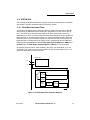
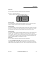
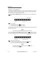
Each UART module, shown in Figure 11-1, consists of the following major functional areas:
¥ Serial Communication Channel
¥ 16-Bit Baud-RateTimer
¥ Internal Channel Control Logic
¥ Interrupt Control Logic
CTS
SERIAL COMMUNICATION
CHANNEL
RTS
RXD
TXD
16-BIT TIMER
FOR BAUD RATE GENERATION
SYSTEM CLOCK
TIN (EXT CLK)
INTERNAL CHANNEL
CONTROL LOGIC
INTERRUPT CONTROL
LOGIC
Figure 11-1. UART Block Diagram
MOTOROLA
MCF5206 USERÕS MANUAL Rev 1.0
11-1
UART Modules
11.1 MODULE OVERVIEW
The MCF5206 contains two independent UART modules. Features of each UART module
include the following:
¥ UART clocked by the system clock or external clock (TIN)
¥ Full duplex asynchronous/synchronous receiver/transmitter channel
¥ Quadruple-buffered receiver
¥ Double-buffered transmitter
¥ Independently programmable baud rate for receiver and transmitter selectable from:
Ñ timer-generated baud rate or external clock
¥ Programmable data format:
Ñ Five to eight data bits plus parity
Ñ Odd, even, no parity, or force parity
Ñ .563 to 2 stop bits in x16 mode(asynchronous)/1or 2 stop bits in synchronous
mode
¥ Programmable channel modes:
Ñ
Ñ
Ñ
Ñ
Normal (full duplex)
Automatic echo
Local loopback
Remote loopback
¥ Automatic wakeup mode for multidrop applications
¥ Four maskable interrupt conditions
¥ Parity, framing, break, and overrun error detection
¥ False start bit detection
¥ Line-break detection and generation
¥ Detection of breaks originating in the middle of a character
¥ Start/end break interrupt/status
11.1.1 Serial Communication Channel
The communication channel provides a full duplex asynchronous/synchronous receiver
and transmitter using an operating frequency derived from the system clock or from an
external clock tied to the TIN pin.
The transmitter accepts parallel data from the CPU; converts it to a serial bit stream;
inserts the appropriate start, stop, and optional parity bits; then outputs a composite serial
data stream on the channel transmitter serial data output (TxD). Refer to Section 11.3.3.1
Transmitter for additional information.
11-2
MCF5206 USERÕS MANUAL Rev 1.0
MOTOROLA
UART Modules
The receiver accepts serial data on the channel receiver serial data input (RxD); converts
it to parallel format; checks for a start bit, stop bit, parity (if any), or any error condition;
and transfers the assembled character onto the bus during read operations. The receiver
can be polled or interrupt driven. Refer to Section 11.3.3.2 Receiver for additional
information.
11.1.2 Baud-Rate Generator/Timer
The 16-bit timer, clocked by the system clock, can function as an asynchronous x16 clock.
In addition, you can tie an external clock to one of the TIN pins of a MCF5206 timer for
use as a synchronous or asynchronous clocking source for the UART. The baud-rate
timer is part of each UART and not related to the ColdFire timer modules.
11.1.3 Interrupt Control Logic
An Internal Interrupt Request signal (IRQ) notifies the MCF5206 interrupt controller of an
interrupt condition. The output is the logical NOR of all (as many as four) unmasked
interrupt status bits in the UART Interrupt Status Register (UISR). You program the UART
Interrupt Mask Register (UIMR) to determine which interrupts will be valid in the UISR.
You program the UART module interrupt level in the MCF5206 interrupt controller
external to the UART module. You can configure the UART to supply the vector from the
UART Interrupt Vector Register (UIVR) or program the SIM to provide an autovector when
a UART interrupt is acknowledged.
You can also program the interrupt level, priority within the level, and autovectoring
capability in the SIM register ICR_U1.
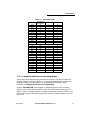
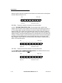
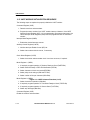
11.2 UART MODULE SIGNAL DEFINITIONS
The following paragraphs contain a brief description of the UART module signals. Figure
11-2 shows both the external and internal signal groups.
NOTE
The terms assertion and negation are used throughout this
section to avoid confusion when dealing with a mixture of
active-low and active-high signals. The term assert or
assertion indicates that a signal is active or true, independent
of the level represented by a high or low voltage. The term
negate or negation indicates that a signal is inactive or false.
11.2.1 Transmitter Serial Data Output (TxD)
This signal is the transmitter serial data output. The output is held high ('ÔmarkÕ' condition)
when the transmitter is disabled, idle, or operating in the local loopback mode. Data is
shifted out on this signal on the falling edge of the clock source, with the least significant
bit transmitted first. All UART pins are muxed with the parallel port. On UART 2, RTS is
MOTOROLA
MCF5206 USERÕS MANUAL Rev 1.0
11-3
UART Modules
muxed with RESET at the pin. Their functionality is determined by programming the Pin
Assignment Register (PAR) in the SIM.
ADDRESSBUS
FOUR-CHARACTER
RECEIVEBUFFER
RXD
TWO-CHARACTER
TRANSMITBUFFER
TXD
LOGIC
DATA
CTS
INPUTPORT
RTS
EXTERNALINTERFACESIGNALS
CONTROL
UARTMODULEINTERNALBUS
INTERFACETOCPU
INTERNAL
CONTROL
OUTPUTPORT
IRQ
16-BITTIMER/
BAUDRATEGENERATOR
SYSTEMCLOCK
TIN(EXTCLK)
Figure 11-2. External and Internal Interface Signals
11.2.2 Receiver Serial Data Input (RxD)
This signal is the receiver serial data input. Data received on this signal is sampled on the
rising edge of the clock source, with the least significant bit received first.
11.2.3 Request-To-Send (RTS)
You can program this active-low output signal to be automatically negated and asserted
by either the receiver or transmitter. When connected to the clear-to-send (CTS) input of
a transmitter, this signal controls serial data flow.
11.2.4 Clear-To-Send (CTS)
This active-low input is the clear-to-send input and can generate an interrupt on changeof-state.
11-4
MCF5206 USERÕS MANUAL Rev 1.0
MOTOROLA
UART Modules
11.3 OPERATION
The following paragraphs describe the operation of the baud-rate generator, transmitter
and receiver, and other operating modes of the UART module.
11.3.1 Baud-Rate Generator/Timer
You should note that the timer references made here relative to clocking the UART are
different than the MCF5206 timer module that is integrated on the bus of the ColdFire
core. The UART has a baud generator based on an internal baud-rate timer that is
dedicated to the UART. You can program the Clock Select Register(USCR) to enable the
baud-rate timer or an external clock source from TIN to generate baud rates. When the
baud-rate timer is used, a prescaler supplies an asynchronous 32x clock source to the
baud-rate timer. The baud-rate timer register value is programmed with the UBG1 and
UBG2 registers. See Section 11.4.1.12 Timer Upper Preload Register 1 (UBG1) and
Section 11.4.1.13 Timer Upper Preload Register 2 (UBG2) for more information.
An external TIN clock source, when enabled in the USCR, can generate an x1 or x16
asynchronous or synchronous clock to the UART receiver and transmitter. Figure 11-3
shows the relationship of clocking sources.
MCF5206 TIMER
TOUT
TIN
MCF5206 UART
BAUD RATE OUTPUT PROGRAMMED INUSCR
x1
PRESCALAR
BAUD
RATE
x16
PRESCALAR
TIMER
OUTPUT
TIN
TIN
INTERNAL
TIMER
x32
PRESCALAR
SYSTEM CLOCK
Figure 11-3. Baud-Rate Timer Generator Diagram
MOTOROLA
MCF5206 USERÕS MANUAL Rev 1.0
11-5
UART Modules
11.3.2 Uart Baud Rate Table
Table 11.1 provides a convenient table for determining standard buad rates on the
MCF5206. The calculation for determining baud rates is as follows:
Baud Rate calculation
baud rate = [Bus clock frequency]/(32*(baud prescale of UBG1&2)
For example, if the bus clock was operating at 45mhz and a 9600 baud rate was needed,
the calculation would be:
9600 = [45 x 10^6]/(32 x UBG1&2 prescale)
The prescale value would be 146 decimal ($0092 hex). Therefore UBG1 (msb) would be
programed with $00 and UBG2 (lsb) would be programmed with $92.
Note
The minimum value that can be programmed into the concatenation of UBG1 and UBG2
is $0002. Also, the values for some of the calculated baud rates below are approximations
due to decimal rounding error (i.e. 9600 baud @ 33mhz is really 9637.85 baud).
Table 11-1. Baud Rate Table
Baud Rate
Decimal Value
for UBG1&2
UBG1
UBG2
300
1200
2400
4800
9600
19.2K
28.8K
33.6K
38.4K
57.6K
67.2K
76800
86400
96000
115200
230400
4688
1172
586
293
146
73
49
42
37
24
21
18
16
15
12
6
12
04
02
01
00
00
00
00
00
00
00
00
00
00
00
00
AF
93
49
24
92
49
30
29
24
18
14
12
10
0E
0C
06
33 MHz bus clock
3438
D
859
3
430
1
215
0
107
0
6D
5B
AD
D6
6B
300
1200
2400
4800
9600
11-6
MCF5206 USERÕS MANUAL Rev 1.0
MOTOROLA
UART Modules
Table 11-1. Baud Rate Table
Baud Rate
19.2K
28.8K
33.6K
38.4K
57.6K
67.2K
76800
86400
96000
115200
230400
300
1200
2400
4800
9600
19.2K
28.8K
33.6K
38.4K
57.6K
67.2K
76800
86400
96000
115200
230400
Decimal Value
for UBG1&2
54
36
31
27
18
15
13
12
11
9
4
UBG1
UBG2
0
0
0
0
0
0
0
0
0
0
0
35
23
1E
1A
11
0F
0D
0B
0A
8
4
22.5 MHz bus clock
2344
9
586
2
293
0
146
0
73
0
37
0
24
0
21
0
18
0
12
0
10
0
9
0
8
0
7
0
6
0
3
0
27
49
24
92
49
24
18
14
12
0C
0A
9
8
7
6
3
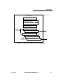
11.3.3 Transmitter and Receiver Operating Modes
The functional block diagram of the transmitter and receiver, including command and
operating registers, is shown in Figure 11-4. The following paragraphs describe these
functions in reference to this diagram. For detailed register information, refer to
subsection 11.4 Register Description and Programming.
11.3.3.1 TRANSMITTER. The transmitter is enabled through the UART command
register (UCR) located within the UART module. The UART module signals the CPU
when it is ready to accept a character by setting the transmitter-ready bit (TxRDY) in the
UART status register (USR). Functional timing information for the transmitter is shown in
Figure 11-5.
MOTOROLA
MCF5206 USERÕS MANUAL Rev 1.0
11-7
UART Modules
The transmitter converts parallel data from the CPU to a serial bit stream on TxD. It
automatically sends a start bit followed by
¥ The programmed number of data bits
¥ An optional parity bit
¥ The programmed number of stop bits
The least significant bit is sent first. Data is shifted from the transmitter output on the falling
edge of the clock source.
After the transmission of the stop bits, if a new character is not available in the transmitter
holding register, the TxD output remains in the high (mark condition) state, and the
transmitter-empty bit (TxEMP) in the USR is set. Transmission resumes and the TxEMP
bit is cleared when the CPU loads a new character into the UART transmitter buffer (UTB).
If the transmitter receives a Disable command, it continues operating until the character
(if one is present) in the transmit-shift register is completely shifted out of transmitter TxD.
If the transmitter is reset through a software command, operation ceases immediately
(refer to subsection Section 11.4.1.5 Command Register (UCR)). The transmitter is reenabled through the UCR to resume operation after a disable or software reset.
If clear-to-send operation is enabled, CTS must be asserted for the character to be
transmitted. If CTS is negated in the middle of a transmission, the character in the shift
register is transmitted and following the completion of STOP bits TxD, enters in the mark
state until CTS is asserted again. If the transmitter is forced to send a continuous low
condition by issuing a Send-Break command, the transmitter ignores the state of CTS.
You can program the transmitter to automatically negate the request-to-send (RTS)
output on completion of a message transmission. If the transmitter is programmed to
operate in this mode, RTS must be manually asserted before a message is transmitted.
In applications where the transmitter is disabled after transmission is complete and RTS
is appropriately programmed, RTS is negated one bit time after the character in the shift
register is completely transmitted. You must manually enable the transmitter by setting
the enable-transmitter bit in the UART Command Register (UCR).
11-8
MCF5206 USERÕS MANUAL Rev 1.0
MOTOROLA
UART Modules
EXTERNAL INTERFACE
UART SERIAL CHANNEL
W
UART COMMAND REGISTER (UCR)
UART MODE REGISTER 1 (UMR1)
R/W
UART MODE REGISTER 2 (UMR2)
R/W
R
UART STATUS REGISTER (USR)
TRANSMIT
BUFFER (UTB)
(2 REGISTERS)
W
TRANSMIT HOLDING REGISTER
TXD
TRANSMIT SHIFT REGISTER
RECEIVER HOLDING REGISTER 1
R
FIFO
RECEIVER HOLDING REGISTER 2
RECEIVER HOLDING REGISTER 3
RECEIVE
BUFFER (URB)
(4 REGISTERS)
RECEIVER SHIFT REGISTER
RXD
Figure 11-4. Transmitter and Receiver Functional Diagram
MOTOROLA
MCF5206 USERÕS MANUAL Rev 1.0
11-9
UART Modules
C1 IN
TRANSMISSION
TxD
TRANSMITTER
ENABLED
C1
C2
C3
C4
BREAK
C6
5
TxRDY
(SR[2])
(SR2)
INTERNAL
MODULE
SELECT
CS
Disable 7
Trans.
W
C1
CTS
W
W
C2
C3
W
START
BREAK
6
W
W
C4
STOP
BREAK
W
W
W
C5
NOT
TRANSMITTED
C6
1
RTS2
MANUALLY ASSERTED
BY BIT- SET COMMAND
Notes:
1. Timing shown for UMR2[4]=1
2. Timing shown for UMR2[5]=1
NOTES:
3.
1. CN=Transmit
TIMING SHOWN8-bit
FORcharacter
UMR2(4) = 1
4. W= Write
2.
TIMING
SHOWN
FOR UMR2(5)
=1
5. Transmitter enabled
by configuring
TCx bits in UCR (see Table 11-9)
3. Start
CN =break/Stop
TRANSMIT CHARACTER
6.
break programmed by MISCx bits in UCR (see Table 11-8)
7.
4. Transmitter
W = WRITE is enabled and disabled using software control
MANUALLY
ASSERTED
Negated since
transmit buffer and
shift register are
empty (last character
has been shifted out)
Figure 11-5. Transmitter Timing Diagram
11-10
MCF5206 USERÕS MANUAL Rev 1.0
MOTOROLA
UART Modules
11.3.3.2 RECEIVER. The receiver is enabled through the UCR located within the UART
module. Functional timing information for the receiver is shown in Figure 11-6. The
receiver looks for a high-to-low (mark-to-space) transition of the start bit on RxD. When a
transition is detected, the state of RxD is sampled each 16´ clock for eight clocks, starting
one-half clock after the transition (asynchronous operation) or at the next rising edge of
the bit time clock (synchronous operation). If RxD is sampled high, the start bit is not valid
and the search for the valid start bit repeats. If RxD is still low, a valid start bit is assumed
and the receiver continues to sample the input at one-bit time intervals at the theoretical
center of the bit.
This process continues until the proper number of data bits and parity (if any) is
assembled and one stop bit is detected. Data on the RxD input is sampled on the rising
edge of the programmed clock source. The least significant bit is received first. The data
is then transferred to a receiver holding register and the RxRDY bit in the USR is set. If
the character length is less than eight bits, the most significant unused bits in the receiver
holding register are cleared. The Rx RDY bit in the USR is set at the one-half point of the
stop bit.
After the stop bit is detected, the receiver immediately looks for the next start bit. However,
if a nonzero character is received without a stop bit (framing error) and RxD remains low
for one-half of the bit period after the stop bit is sampled, the receiver operates as if a new
start bit is detected. The parity error (PE), framing error (FE), overrun error (OE), and
received break (RB) conditions (if any) set error and break flags in the USR at the received
character boundary and are valid only when the RxRDY bit in the USR is set.
If a break condition is detected (RxD is low for the entire character including the stop bit),
a character of all zeros is loaded into the receiver holding register and the Receive Break
(RB) and RxRDY bits in the USR are set. The RxD signal must return to a high condition
for at least one-half bit time before a search for the next start bit begins.
The receiver will detect the beginning of a break in the middle of a character if the break
persists through the next character time. When the break begins in the middle of a
character, the receiver places the damaged character in the receiver first-in-first-out
(FIFO) stack and sets the corresponding error conditions and RxRDY bit in the USR. The
break persists until the next character time, the receiver places an all-zero character into
the receiver FIFO, and sets the corresponding RB and RxRDY bits in the USR. Interrupts
can be enabled on receive break.
MOTOROLA
MCF5206 USERÕS MANUAL Rev 1.0
11-11
UART Modules
C2
C1
RxD
C3
C4
C5
C6
C8
C7
C6, C7, C8 ARE LOST DUE TO
RECEIVER DISABLED
RECEIVER
ENABLED
RxRDY
(SR0)
2
2.5
FFULL
(SR1)
INTERNAL
MODULE
SELECT
CS
R
R
R R
R R R R
STATUS DATA STATUS DATA STATUS DATA
STATUS DATA
C2
C1
C3
C4
C5
LOST
OVERRUN
(SR4)
1
RTS
(OP0)
RESET BY COMMAND
UOP1[0]=1
UOP(0)
=1
NOTES:
1. Timing shown for UMR1[7]=1
NOTES:
2. Timing shown for UMR1[6]=0
2.5Timing
1. Timingshown
shownforforUMR1[6]=1
MR1(7) = 1
3.2.R=Read
Timing shown for MR1(6) = 0
4.3.CN=Received
5-8
bit
character
R = Read
4. C = Received Character
N
Figure 11-6. Receiver Timing Diagram
11-12
MCF5206 USERÕS MANUAL Rev 1.0
MOTOROLA
UART Modules
11.3.3.3 FIFO STACK. The FIFO stack is used in the UART receiver buffer logic. The
FIFO stack consists of three receiver holding registers. The receive buffer consists of the
FIFO and a receiver shift register connected to the RxD (refer to Figure 11-4). Data is
assembled in the receiver shift register and loaded into the top empty receiver holding
register position of the FIFO. Thus, data flowing from the receiver to the CPU is quadruple
buffered.
In addition to the data byte, three status bits, parity error (PE), framing error (FE), and
received break (RB) are appended to each data character in the FIFO; overrun error (OE)
is not appended. By programming the error-mode bit (ERR) in the channel's mode register
(UMR1), you can provide status in character or block modes.
The RxRDY bit in the USR is set whenever one or more characters are available to be
read by the CPU. A read of the receiver buffer produces an output of data from the top of
the FIFO stack. After the read cycle, the data at the top of the FIFO stack and its
associated status bits are Ô'popped,'Õ and the receiver shift register can add new data at
the bottom of the stack. The FIFO-full status bit (FFULL) is set if all three stack positions
are filled with data. Either the RxRDY or FFULL bit can be selected to cause an interrupt.
In the character mode, status provided in the USR is given on a character-by-character
basis and thus applies only to the character at the top of the FIFO. In the block mode, the
status provided in the USR is the logical OR of all characters coming to the top of the FIFO
stack since the last reset error command. A continuous logical OR function of the
corresponding status bits is produced in the USR as each character reaches the top of
the FIFO stack.
The block mode is useful in applications where the software overhead of checking each
character's error cannot be tolerated. In this mode, entire messages are received and only
one data integrity check is performed at the end of the message. This mode has a datareception speed advantage; however, each character is not individually checked for error
conditions by software. If an error occurs within the message, the error is not recognized
until the final check is performed, and no indication exists as to which message character
is at fault.
In either mode, reading the USR does not affect the FIFO. The FIFO is popped only when
the receive buffer is read. The USR should be read prior to reading the receive buffer. If
all three of the FIFO receiver holding registers are full when a new character is received,
the new character is held in the receiver shift register until a FIFO position is available. If
an additional character is received during this state, the contents of the FIFO are not
affected. However, the previous character in the receiver shift register is lost and the OE
bit in the USR is set when the receiver detects the start bit of the new overrunning
character.
To support control flow capability, you can program the receiver to automatically negate
and assert RTS. When in this mode, the receiver automatically negates RTS when a valid
start bit is detected and the FIFO stack is full. When a FIFO position becomes available,
MOTOROLA
MCF5206 USERÕS MANUAL Rev 1.0
11-13
UART Modules
the receiver asserts RTS. Using this mode of operation prevents overrun errors by
connecting the RTS to the CTS input of the transmitting device.
To use the RTS signals on UART 2, you must set up the MCF5206 Pin Assignment
Register (PAR) in the SIM to enable the corresponding I/O pins for these functions. If the
FIFO stack contains characters and the receiver is disabled, the CPU can still read the
characters in the FIFO. If the receiver is reset, the FIFO stack and all receiver status bits,
corresponding output ports, and interrupt request are reset. No additional characters are
received until the receiver is re-enabled.
11.3.4 Looping Modes
You can configure the UART to operate in various looping modes as shown in Figure 117. These modes are useful for local and remote system diagnostic functions. The modes
are described in the following paragraphs with additional information available in
subsection 11.4 Register Description and Programming.
You should only switch between modes while the transmitter and receiver are disabled
because the selected mode will be activated immediately on mode selection, even if this
occurs in the middle of character transmission or reception. In addition, if a mode is
deselected, the device will switch out of the mode immediately, except for automatic echo
and remote echo loopback modes. In these modes, the deselection will occur just after
the receiver has sampled the stop bit (this is also the one-half point). For automatic echo
mode, the transmitter will stay in this mode until the entire stop bit has been retransmitted.
11.3.4.1 AUTOMATIC ECHO MODE. In this mode, the UART automatically retransmits
the received data on a bit-by-bit basis. The local CPU-to-receiver communication
continues normally but the CPU-to-transmitter link is disabled. While in this mode,
received data is clocked on the receiver clock and retransmitted on TxD. The receiver
must be enabled but not the transmitter. Instead, the transmitter is clocked by the receiver
clock.
Because the transmitter is not active, the TxEMP and TxRDY bits in USR are inactive and
data is transmitted as it is received. Received parity is checked but not recalculated for
transmission. Character framing is also checked but stop bits are transmitted as received.
A received break is echoed as received until the next valid start bit is detected.
11.3.4.2 LOCAL LOOPBACK MODE. In this mode, TxD is internally connected to RxD.
This mode is useful for testing the operation of a local UART module channel by sending
data to the transmitter and checking data assembled by the receiver. In this manner,
correct channel operations can be assured. Both transmitter and CPU-to-receiver
communications continue normally in this mode. While in this mode, the RxD input data
is ignored, the TxD is held marking, and the receiver is clocked by the transmitter clock.
The transmitter must be enabled but not the receiver.
11.3.4.3 REMOTE LOOPBACK MODE. In this mode, the channel automatically
transmits received data on the TxD output on a bit-by-bit basis. The local CPU-to-
11-14
MCF5206 USERÕS MANUAL Rev 1.0
MOTOROLA
UART Modules
transmitter link is disabled. This mode is useful for testing remote channel receiver and
transmitter operation. While in this mode, the receiver clocks the transmitter.
Because the receiver is not active, the CPU cannot read received data. All status
conditions are inactive. Received parity is not checked and is not recalculated for
transmission. Stop bits are transmitted as received. A received break is echoed as
received until the next valid start bit is detected.
RxD
INPUT
Rx
CPU
DISABLED
Tx
DISABLED
TxD
OUTPUT
(a) Automatic Echo
Rx
DISABLED
RxD
INPUT
DISABLED
TxD
OUTPUT
CPU
Tx
(b) Local Loopback
DISABLED
Rx
DISABLED
RxD
INPUT
DISABLED
TxD
OUTPUT
CPU
DISABLED
Tx
(c) Remote Loopback
Figure 11-7. Looping Modes Functional Diagram
MOTOROLA
MCF5206 USERÕS MANUAL Rev 1.0
11-15
UART Modules
11.3.5 Multidrop Mode
You can program the UART to operate in a wakeup mode for multidrop or multiprocessor
applications. Functional timing information for the multidrop mode is shown in Figure 118. You select the mode by setting bits 3 and 4 in UART mode register 1 (UMR1). This
mode of operation connects the master station to several slave stations (maximum of
256). In this mode, the master transmits an address character followed by a block of data
characters targeted for one of the slave stations. The slave stations channel receivers are
disabled; however, they continuously monitor the data stream sent out by the master
station. When the master sends an address character, the slave receiver channel notifies
its respective CPU by setting the RxRDY bit in the USR and generating an interrupt (if
programmed to do so). Each slave station CPU then compares the received address to
its station address and enables its receiver if it wants to receive the subsequent data
characters or block of data from the master station. Slave stations not addressed continue
to monitor the data stream for the next address character. Data fields in the data stream
are separated by an address character. After a slave receives a block of data, the slave
station CPU disables the receiver and reinitiates the process.
A transmitted character from the master station consists of a start bit, a programmed
number of data bits, an address/data (A/D) bit flag, and a programmed number of stop
bits. The A/D bit identifies the type of character being transmitted to the slave station. The
character is interpreted as an address character if the A/D bit is set or as a data character
if the A/D bit is cleared. You select the polarity of the A/D bit by programming bit 2 of
UMR1. You should also program UMR1 before enabling the transmitter and loading the
corresponding data bits into the transmit buffer.
In multidrop mode, the receiver continuously monitors the received data stream,
regardless of whether it is enabled or disabled. If the receiver is disabled, it sets the
RxRDY bit and loads the character into the receiver holding register FIFO stack, provided
the received A/D bit is a one (address tag). The character is discarded if the received
A/D bit is a zero (data tag). If the receiver is enabled, all received characters are
transferred to the CPU via the receiver holding register stack during read operations.
In either case, the data bits are loaded into the data portion of the stack while the A/D bit
is loaded into the status portion of the stack normally used for a parity error (USR bit 5).
Framing error, overrun error, and break detection operate normally. The A/D bit takes the
place of the parity bit; therefore, parity is neither calculated nor checked. Messages in this
mode can still contain error detection and correction information. One way to provide error
detection, if 8-bit characters are not required, is to use software to calculate parity and
append it to the 5-, 6-, or 7-bit character.
11-16
MCF5206 USERÕS MANUAL Rev 1.0
MOTOROLA
UART Modules
MASTER STATION
A/D
A/D
TxD
ADDR
1
1
C0
A/D
ADDR
1
2
0
TRANSMITTER
ENABLED
TxRDY
(USR2)
INTERNAL
CS
MODULE
SELECT
W
W
UMR1[4:3]=11
UMR1(4:3) = 11
UMR1[2]=1
UMR1(2) = 1
PERIPHERAL
STATION
RxD
W
W
W
A/D
A/D
0
ADDR2
A/D
A/D
A/D
ADDR
1
1
W
UMR1[2]=1
UMR1(2)
=1
UMR1[2]=0
=0
ADDR1 UMR1(2)
C0
A/D
A/D
A/D
ADDR
1
2
0
0
RECEIVER
ENABLED
INTERNAL
CS
MODULE
SELECT
W
UMR1(4Ð3) = 11
W R
ENABLE ADDR
R
R
STATUS DATA
R
R
STATUS DATA
C0
ADDR
Figure 11-8. Multidrop Mode Timing Diagram
MOTOROLA
MCF5206 USERÕS MANUAL Rev 1.0
11-17
UART Modules
11.3.6 Bus Operation
This subsection describes the operation of the bus during read, write, and interruptacknowledge cycles to the UART module. All UART module registers must be accessed
as bytes.
11.3.6.1 READ CYCLES. The CPU with zero wait states accesses the UART module
because the MCF5206 system clock is also used for the UART module. The UART
module responds to reads with byte data on D[7:0]. Reserved registers return logic zero
during reads.
11.3.6.2 WRITE CYCLES. The CPU with zero wait states accesses the UART module.
The UART module accepts write data on D[7:0]. Write cycles to read-only registers and
reserved registers complete in a normal manner without exception processing; however,
the data is ignored.
11.3.6.3 INTERRUPT ACKNOWLEDGE CYCLES. The UART module can arbitrate for
interrupt servicing and supply the interrupt vector when it has successfully won arbitration.
The vector number must be provided if interrupt servicing is necessary; thus, the interrupt
vector register (UIVR) must be initialized. The interrupt vector number generated by the
IVR is used if the autovector is not enabled in the SIM Interrupt Control Register (ICR). If
the UIVR is not initialized and the ICR is not programmed for autovector, a spurious
interrupt exception is taken if interrupts are generated. This works in conjunction with the
MCF5206 interrupt controller, which allows a programmable Interrupt Priority Level (IPL)
for the interrupt.
11.4 REGISTER DESCRIPTION AND PROGRAMMING
This subsection contains a detailed description of each register and its specific function
as well as flowcharts of basic UART module programming.
11.4.1 Register Description
Writing control bytes into the appropriate registers controls the UART operation. A list of
UART module registers and their associated addresses is shown in Table 11-2.
NOTE
All UART module registers are accessible only as bytes. You
should change the contents of the mode registers (UMR1 and
UMR2), clock-select register (UCSR), and the auxiliary control
register (UACR) bit 7 only after the receiver/transmitter is
issued a software RESET commandÑi.e., channel operation
must be disabled. You should be careful if the register
contents are changed during receiver/transmitter operations
as unpredictable results can occur.
For the registers discussed in the following pages, the numbers above the register
description represent the bit position in the register. The register description contains the
11-18
MCF5206 USERÕS MANUAL Rev 1.0
MOTOROLA
UART Modules
mnemonic for the bit. The values shown below the register description are the values of
those register bits after a hardware reset. A value of U indicates that the bit value is
unaffected by reset. The read/write status is shown in the last line.
Table 11-2. UART Module Programming Model
UART1 2
UART1
REGISTER READ (R/W = 1)
REGISTER WRITE (R/W = 0)
MBAR+$188 MBAR+$148
Mode Register (UMR1, UMR2)
Status Register (USR)
DO NOT ACCESS1
Command Register (UCR)
MBAR+$18C
MBAR+$190
MBAR+$194
MBAR+$198
MBAR+$19C
Receiver Buffer (URB)
Input Port Change Register (UIPCR)
Interrupt Status Register (UISR)
Baud Rate Generator Prescale MSB (UBG1)
Baud Rate Generator Prescale LSB (UBG2)
Transmitter Buffer (UTB)
Auxiliary Control Register (UACR)
Interrupt Mask Register (UIMR)
Baud Rate Generator Prescale MSB (UBG1)
Baud Rate Generator Prescale LSB (UBG2)
MBAR+$180 MBAR+$140
MBAR+$184 MBAR+$144
MBAR+$14C
MBAR+$150
MBAR+$154
MBAR+$158
MBAR+$15C
Mode Register (UMR1, UMR2)
Clock-Select Register (UCSR)
DO NOT ACCESS1
MBAR+$1B0 MBAR+$170
Interrupt Vector Register (UIVR)
INterrupt Vector Register (UIVR)
MBAR+$1B4 MBAR+$174
Input Port Register (UIP)
DO NOT ACCESS1
MBAR+$1B8 MBAR+$178
DO NOT ACCESS1
DO NOT ACCESS1
Output Port Bit Set CMD (UOP1)2
Output Port Bit Reset CMD (UOP0)2
This address is used for factory testing and should not be read. Reading this location results in undesired effects and possible
incorrect transmission or reception of characters. Register contents can also be changed.
MBAR+$1BC MBAR+$17C
NOTES: 1.
2.
Address-triggered commands.
11.4.1.1 MODE REGISTER 1 (UMR1). UMR1 controls some of the UART module
configuration. This register can be read or written at any time and is accessed when the
mode register pointer points to UMR1. The pointer is set to UMR1 by RESET or by a set
pointer command using the control register. After reading or writing UMR1, the pointer
points to UMR2.
UMR1
7
MBAR + $140
6
RXRTS RXIRQ
5
4
3
2
1
0
ERR
PM1
PM0
PT
B/C1
B/C0
0
0
0
0
0
0
RESET
0
0
READ/WRITE
SUPERVISOR OR USER
RxRTS Ñ Receiver Request-to-Send Control
1 = On receipt of a valid start bit, RTS is negated if the UART FIFO is full. RTS is
reasserted when the FIFO has an empty position available.
0 = The receiver has no effect on RTS. The RTS is asserted by writing a one to the
Output Port Bit Set Register (UOP1)
MOTOROLA
MCF5206 USERÕS MANUAL Rev 1.0
11-19
UART Modules
You can use this feature for flow control to prevent overrun in the receiver by using the
RTS output to control the CTS input of the transmitting device. If both the receiver and
transmitter are programmed for RTS control, RTS control is disabled for both because
such a configuration is incorrect. See Section 11.4.1.2 Mode Register 2 (UMR2) for
information on programming the transmitter RTS control. On UART 2, RTS is muxed.
RxIRQ Ñ Receiver Interrupt Select
1 = FFULL is the source that generates IRQ
0 = RxRDY is the source that generates IRQ
ERR Ñ Error Mode
This bit controls the meaning of the three FIFO status bits (RB, FE, and PE) in the USR.
1 = Block modeÑThe values in the channel USR are the accumulation (i.e., the
logical OR) of the status for all characters coming to the top of the FIFO since
the last reset error status command for the channel was issued. Refer to Section
11.4.1.5 Command Register (UCR) for more information on UART module
commands.
0 = Character modeÑThe values in the channel USR reflect the status of the
character at the top of the FIFO.
NOTE
You must use ERR = 0 to obtain the correct A/D flag
information when in multidrop mode.
PM1ÐPM0 Ñ Parity Mode
These bits encode the type of parity used for the channel (see Table 11-3). The parity bit
is added to the transmitted character and the receiver performs a parity check on
incoming data. These bits can alternatively select multidrop mode for the channel.
PT Ñ Parity Type
This bit selects the parity type if parity is programmed by the parity mode bits; if multidrop
mode is selected, it configures the transmitter for data character transmission or address
character transmission. Table 11-3 lists the parity mode and type or the multidrop mode
for each combination of the parity mode and the parity type bits.
Table 11-3. PMx and PT Control Bits
11-20
PM1
PM0
PARITY MODE
PT
PARITY TYPE
0
0
0
0
1
1
1
0
0
1
1
0
1
1
With Parity
With Parity
Force Parity
Force Parity
No Parity
Multidrop Mode
Multidrop Mode
0
1
0
1
X
0
1
Even Parity
Odd Parity
Low Parity
High Parity
No Parity
Data Character
Address Character
MCF5206 USERÕS MANUAL Rev 1.0
MOTOROLA
UART Modules
ÒForce parity lowÓ means forcing a 0 parity bit. ÒForce parity highÓ forces a 1 parity bit.
B/C1ÐB/C0 Ñ Bits per Character
These bits select the number of data bits per character to be transmitted. The character
length listed in Table 11-4 does not include start, parity, or stop bits.
Table 11-4. B/Cx Control Bits
B/C1
B/C0
BITS/CHARACTER
0
0
5 Bits
0
1
6 Bits
1
0
7 Bits
1
1
8 Bits
11.4.1.2 MODE REGISTER 2 (UMR2). UMR2 controls some of the UART module
configuration. It is accessed when the mode register pointer points to UMR2, which occurs
after any access to UMR1. Accesses to UMR2 do not change the pointer.
UMR2
MBAR + $180
7
6
CM1
CM0
5
4
TXRTS TXCTS
3
2
1
0
SB3
SB2
SB1
SB0
0
0
0
0
RESET:
0
0
0
0
READ/WRITE
SUPERVISOR OR USER
CM1ÐCM0 Ñ Channel Mode
These bits select a channel mode as listed in Table 11-5. See Section 11.3.4 Looping
Modes for more information on the individual modes.
Table 11-5. CMx Control Bits
CM1
CM0
MODE
0
0
1
1
0
1
0
1
Normal
Automatic Echo
Local Loopback
Remote Loopback
TxRTS Ñ Transmitter Ready-to-Send
This bit controls the negation of the RTS signal.
In applications where the transmitter is disabled after transmission is complete, setting
this bit causes the OP bit to be cleared automatically one bit time after the characters (if
any) in the channel transmit shift register and the transmitter holding register are
completely transmitted, including the programmed number of stop bits. This feature
automatically terminates message transmission. You can perform this process by
following these steps:
MOTOROLA
MCF5206 USERÕS MANUAL Rev 1.0
11-21
UART Modules
1. Program the UART for the automatic-reset mode: UMR2[5]=1
2. Enable the transmitter
3. Assert the transmitter request-to send control: UOP1[0]=1
4. Send the message
5. Disable the transmitter after the TxRDY bit but not the TxEMP bit in the USR
becomes asserted.
The last character will be transmitted and the UOP0[0] bit will be set causing the
transmitter request-to-send control to be negated.
If both the receiver and the transmitter in the same channel are programmed for RTS
control, RTS control is disabled for both because of this incorrect configuration.
1 = If both TxRDY and TXEMP bits in the UART Status Register (USR) are set, there
will be no change on RTS. For TXRTS to be set to 1 in this condition, you must
set the UART Output Port Set Data Register (UOP1).
0 = The transmitter has no effect on RTS.
TxCTS Ñ Transmitter Clear-to-Send
1 = Enables clear-to-send operation. The transmitter checks the state of the CTS
input each time it is ready to send a character. If CTS is asserted, the character
is transmitted. If CTS is negated, the channel TxD remains in the high state
(mark condition) and the transmission is delayed until CTS is asserted. Changes
in CTS while a character is being transmitted do not affect transmission of that
character.
0 = The CTS has no effect on the transmitter.
SB3ÐSB0 Ñ Stop-Bit Length Control
These bits select the length of the stop bit appended to the transmitted character as listed
in Table 11-6. Stop-bit lengths of 9/16 to two bits, in increments of 1/16 bit, are
programmable for character lengths of six, seven, and eight bits. For a character length
of five bits, 1-1/16 to two bits are programmable in increments of 1/16 bit. In all cases, the
receiver only checks for a high condition at the center of the first stop-bit positionÑi.e.,
one bit time after the last data bit or after the parity bit, if parity is enabled.
If an external 1´ clock is used for the transmitter, UMR2 bit 3 = 0 selects one stop bit, and
UMR2 bit 3 = 1 selects two stop bits for transmission.
Table 11-6. SBx Control Bits
11-22
SB3
SB2
SB1
SB0
LENGTH 6-8 BITS
LENGTH 5 BITS
0
0
0
0
0
0
0
0
0
0
1
1
0
1
0
1
0.563
0.625
0.688
0.750
1.063
1.125
1.188
1.250
MCF5206 USERÕS MANUAL Rev 1.0
MOTOROLA
UART Modules
Table 11-6. SBx Control Bits (Continued)
0
0
0
0
1
1
1
1
1
1
1
1
1
1
1
1
0
0
0
0
1
1
1
1
0
0
1
1
0
0
1
1
0
0
1
1
0
1
0
1
0
1
0
1
0
1
0
1
0.813
0.875
0.938
1.000
1.563
1.625
1.688
1.750
1.813
1.875
1.938
2.000
1.313
1.375
1.438
1.500
1.563
1.625
1.688
1.750
1.813
1.875
1.938
2.000
11.4.1.3 STATUS REGISTER (USR). The USR indicates the status of the characters in
the receive FIFO and the status of the transmitter and receiver. The RB, FE, and PE bits
USR
MBAR + $184
7
6
5
4
RB
FE
PE
OE
0
0
0
3
2
1
0
TXEMP TXRDY FFULL RXRDY
RESET:
0
READ ONLY
0
0
0
0
SUPERVISOR OR USER
are cleared by the Reset Error Status command in the UCR if the RB bit has not been
read. Also, RB, FE, PE and OE can also be cleared by reading the Receive buffer (RE).
RB Ñ Received Break
1 = An all-zero character of the programmed length has been received without a
stop bit. The RB bit is valid only when the RxRDY bit is set. A single FIFO
position is occupied when a break is received. Additional entries into the FIFO
are inhibited until RxD returns to the high state for at least one-half bit time, which
is equal to two successive edges of the internal or external 1´ clock or 16
successive edges of the external 16´ clock. The received break circuit detects
breaks that originate in the middle of a received character. However, if a break
begins in the middle of a character, it must persist until the end of the next
detected character time.
0 = No break has been received.
FE Ñ Framing Error
1 = A stop bit was not detected when the corresponding data character in the FIFO
was received. The stop-bit check occurs in the middle of the first stop-bit
position. The bit is valid only when the RxRDY bit is set.
0 = No framing error has occurred.
MOTOROLA
MCF5206 USERÕS MANUAL Rev 1.0
11-23
UART Modules
PE Ñ Parity Error
1 = When the with-parity or force-parity mode is programmed in the UMR1, the
corresponding character in the FIFO was received with incorrect parity. When
the multidrop mode is programmed, this bit stores the received A/D bit. This bit
is valid only when the RxRDY bit is set.
0 = No parity error has occurred.
OE Ñ Overrun Error
1 = One or more characters in the received data stream have been lost. This bit is
set on receipt of a new character when the FIFO is full and a character is already
in the shift register waiting for an empty FIFO position. When this occurs, the
character in the receiver-shift register and its break-detect, framing-error status,
and parity error, if any, are lost. The reset-error status command in the UCR
clears this bit.
0 = No overrun has occurred.
11-24
MCF5206 USERÕS MANUAL Rev 1.0
MOTOROLA
UART Modules
TxEMP Ñ Transmitter Empty
1 = The transmitter has underrun (both the transmitter holding register and
transmitter shift registers are empty). This bit is set after transmission of the last
stop bit of a character if there are no characters in the transmitter-holding register
awaiting transmission.
0 = The transmitter buffer is not empty. Either a character is currently being shifted
out or the transmitter is disabled. You can enable/disable the transmitter by
programming the TCx bits in the UCR.
TxRDY Ñ Transmitter Ready
1 = The transmitter-holding register is empty and ready to be loaded with a
character. This bit is set when the character is transferred to the transmitter shift
register. This bit is also set when the transmitter is first enabled. Characters
loaded into the transmitter holding register while the transmitter is disabled are
not transmitted.
0 = The CPU has loaded the transmitter-holding register or the transmitter is
disabled.
FFULL Ñ FIFO Full
1 = Three characters have been received and are waiting in the receiver buffer
FIFO.
0 = The FIFO is not full but can contain as many as two unread characters.
RxRDY Ñ Receiver Ready
1 = One or more characters have been received and are waiting in the receiver
buffer FIFO.
0 = The CPU has read the receiver buffer and no characters remain in the FIFO after
this read.
MOTOROLA
MCF5206 USERÕS MANUAL Rev 1.0
11-25
UART Modules
11.4.1.4 CLOCK-SELECT REGISTER (UCSR). The UCSR selects the internal clock
(timer mode) or the external clock in synchronous or asynchronous mode. To use the
timer mode for either the receiver and transmitter channel, program the UCSR to the value
$DD. The transmitter and receiver can be programmed to different clock sources.
UCSR
MBAR + $184
7
6
5
4
3
2
1
0
RCS3
RCS2
RCS1
RCS0
TCS3
TCS2
TCS1
TCS0
1
0
1
1
1
0
1
RESET:
1
WRITE ONLY
SUPERVISOR OR USER
RCS3ÐRCS0 Ñ Receiver Clock Select
These bits select the clock source for the receiver channel. Table 11-7 details the register
bits necessary for each mode.
Table 11-7. RCSx Control Bits
RCS3
RCS2
RCS1
RCS0
MODE
1
1
1
1
1
1
0
1
1
1
0
1
TIMER
Ext. clk. x 16
Ext. clk. x 1
TCS3ÐTCS0 Ñ Transmitter Clock Select
These bits determine the clock source of the UART transmitter channel.
Table 11-8. TCSx Control Bits
TCS3
TCS2
TCS1
TCS0
SET 1
1
1
1
1
1
1
0
1
1
1
0
1
TIMER
Ext. clk. x 16
Ext. clk. x 1
11.4.1.5 COMMAND REGISTER (UCR). The UCR supplies commands to the UART.
You can specify multiple commands in a single write to the UCR if the commands are not
conflicting Ð e.g., reset-transmitter and enable-transmitter commands cannot be specified
in a single command.
UCR
7
Ñ
MBAR + $188
6
5
4
MISC2 MISC1 MISC0
3
2
1
0
TC1
TC0
RC1
RC0
0
0
0
0
RESET:
0
0
WRITE ONLY
11-26
0
0
SUPERVISOR OR USER
MCF5206 USERÕS MANUAL Rev 1.0
MOTOROLA
UART Modules
MISC3ÐMISC0 Ñ Miscellaneous Commands
These bits select a single command as listed in Table 11-9.
Table 11-9. MISCx Control Bits
MISC2
MISC1
MISC0
COMMAND
0
0
0
0
1
1
1
1
0
0
1
1
0
0
1
1
0
1
0
1
0
1
0
1
No Command
Reset Mode Register Pointer
Reset Receiver
Reset Transmitter
Reset Error Status
Reset Break-Change Interrupt
Start Break
Stop Break
The commands are described as follows:
Reset Mode Register Pointer
The reset mode register pointer command causes the mode register pointer to point to
UMR1.
Reset Receiver
The reset receiver command resets the receiver. The receiver is immediately disabled,
the FFULL and RxRDY bits in the USR are cleared, and the receiver FIFO pointer is
reinitialized. All other registers are unaltered. Use this command instead of the receiverdisable command whenever the receiver configuration is changed (it places the receiver
in a known state).
Reset Transmitter
The reset transmitter command resets the transmitter. The transmitter is immediately
disabled and the TxEMP and TxRDY bits in the USR are cleared. All other registers are
unaltered. Use this command instead of the transmitter-disable command whenever the
transmitter configuration is changed (it places the transmitter in a known state).
Reset Error Status
The reset error status command clears the RB, FE, PE, and OE bits in the USR. This
command is also used in the block mode to clear all error bits after a data block is
received.
Reset Break-Change Interrupt
The reset break-change interrupt command clears the delta break (DBx) bit in the UISR.
MOTOROLA
MCF5206 USERÕS MANUAL Rev 1.0
11-27
UART Modules
Start Break
The start break command forces TxD low. If the transmitter is empty, the start of the break
conditions can be delayed by as much as two bit times. If the transmitter is active, the
break begins when transmission of the character is complete. If a character is in the
transmitter shift register, the start of the break is delayed until the character is transmitted.
If the transmitter holding register has a character, that character is transmitted before the
break. The transmitter must be enabled for this command to be accepted. The state of the
CTS input is ignored for this command.
Stop Break
The stop break command causes TxD to go high (mark) within two bit times. Characters
stored in the transmitter buffer, if any, are transmitted.
TC1ÐTC0 Ñ Transmitter Commands
These bits select a single command as listed in Table 11-10.
Table 11-10. TCx Control Bits
TC1
TC0
COMMAND
0
0
1
1
0
1
0
1
No Action Taken
Transmitter Enable
Transmitter Disable
Do Not Use
The definitions of the transmitter command options are as follows:
No Action Taken
The ÔÔno action takenÕÕ command causes the transmitter to stay in its current mode. If the
transmitter is enabled, it remains enabled; if disabled, it remains disabled.
Transmitter Enable
The ÔÔtransmitter enableÕÕ command enables operation of the channel's transmitter. The
TxEMP and TxRDY bits in the USR are also set. If the transmitter is already enabled, this
command has no effect.
Transmitter Disable
The ÔÔtransmitter disableÕÕ command terminates transmitter operation and clears the
TxEMP and TxRDY bits in the USR. However, if a character is being transmitted when the
transmitter is disabled, the transmission of the character is completed before the
transmitter becomes inactive. If the transmitter is already disabled, this command has no
effect.
11-28
MCF5206 USERÕS MANUAL Rev 1.0
MOTOROLA
UART Modules
Do Not Use
Do not use this bit combination because the result is indeterminate.
RC1ÐRC0 Ñ Receiver Commands
These bits select a single command as listed in Table 11-11.
Table 11-11. RCx Control Bits
RC1
RC0
COMMAND
0
0
1
1
0
1
0
1
No Action Taken
Receiver Enable
Receiver Disable
Do Not Use
No Action Taken
The ÔÔno action takenÕÕ command causes the receiver to stay in its current mode. If the
receiver is enabled, it remains enabled; if disabled, it remains disabled.
Receiver Enable
The ÔÔreceiver enableÕÕ command enables operation of the channel's receiver. If the UART
module is not in multidrop mode, this command also forces the receiver into the searchfor-start-bit state. If the receiver is already enabled, this command has no effect.
Receiver Disable
The ÔÔreceiver disableÕÕ command immediately disables the receiver. Any character being
received is lost. The command has no effect on the receiver status bits or any other
control register. If the UART module is programmed to operate in the local loopback mode
or multidrop mode, the receiver operates even though this command is selected. If the
receiver is already disabled, this command has no effect.
Do Not Use
Do not use this bit combination because the result is indeterminate.
11.4.1.6 RECEIVER BUFFER (URB). The receiver buffer contains three receiverholding registers and a serial shift register. The RxD pin is connected to the serial shift
register while the holding registers act as a FIFO. The CPU reads from the top of the stack
MOTOROLA
MCF5206 USERÕS MANUAL Rev 1.0
11-29
UART Modules
while the receiver shifts and updates from the bottom of the stack when the shift register
has been filled (see Figure 11-4).
URB
MBAR + $18C
7
6
5
4
3
2
1
0
RB7
RB6
RB5
RB4
RB3
RB2
RB1
RB0
1
1
1
1
1
1
1
RESET:
1
READ ONLY
SUPERVISOR OR USER
RB7ÐRB0 Ñ These bits contain the character in the receiver buffer.
11.4.1.7 TRANSMITTER BUFFER (UTB). The transmitter buffer consists of two
registers: the transmitter-holding register and the transmitter shift register (see Figure 114). The holding register accepts characters from the bus master if the TxRDY bit in the
channel's USR is set. A write to the transmitter buffer clears the TxRDY bit, inhibiting
additional characters until the shift register is ready to accept more data. When the shift
register is empty, it checks the holding register for a valid character to be sent (TxRDY bit
cleared). If a valid character is present, the shift register loads the character and reasserts
the TxRDY bit in the USR. Writes to the transmitter buffer when the channel's UART
Status Register (USR) TxRDY bit is clear and when the transmitter is disabled have no
effect on the transmitter buffer.
UTB
MBAR + $18C
7
6
5
4
3
2
1
0
TB7
TB6
TB5
TB4
TB3
TB2
TB1
TB0
0
0
0
0
0
0
0
RESET:
0
WRITE ONLY
SUPERVISOR OR USER
TB7ÐTB0 Ñ These bits contain the character in the transmitter buffer.
11.4.1.8 INPUT PORT CHANGE REGISTER (UIPCR). The UIPCR shows the current
state and the change-of-state for the CTS pin.
UIPCR
MBAR + $190
7
6
5
4
3
2
1
0
0
0
0
COS
1
1
1
CTS
0
0
0
1
1
1
1
RESET:
0
READ ONLY
11-30
SUPERVISOR OR USER
MCF5206 USERÕS MANUAL Rev 1.0
MOTOROLA
UART Modules
Bits 7, 6, 5, 3, 2, 1 Ñ Reserved by Motorola.
COS Ñ Change-of-State
1 = A change-of-state (high-to-low or low-to-high transition), lasting longer than 25Ð
50 ms has occurred at the CTS input. When this bit is set, you can program the
UART Auxiliary Control Register (UACR) to generate an interrupt to the CPU.
0 = No change-of-state has occurred since the last time the CPU read the UART
Input Port Change Register (UIPCR). A read of the UIPCR also clears the UART
Interrupt Status Register (UISR)COS bit.
CTS Ñ Current State
Starting two serial clock periods after reset, the CTS bit reflects the state of the CTS pin.
If the CTS pin is detected as asserted at that time, the COS bit is set, which initiates an
interrupt if the Input Enable Control (IEC) bit of the UACR register is enabled.
1 = The current state of the CTS input is logic one.
0 = The current state of the CTS input is logic zero.
11.4.1.9 AUXILIARY CONTROL REGISTER (UACR). The UACR selects the
appropriate baud rate and controls the handshake of the transmitter/receiver.
UACR
MBAR + $190
7
6
5
4
3
2
1
0
-
-
-
-
-
-
-
IEC
0
0
0
0
0
0
0
RESET:
0
WRITE ONLY
SUPERVISOR OR USER
IEC Ñ Input Enable Control
1 = UISR bit 7 is set and generates an interrupt when the COS bit in the UART Input
Port Change Register (UIPCR) is set by an external transition on the CTS input
(if bit 7 of the interrupt mask register (UIMR) is set to enable interrupts).
0 = Setting the corresponding bit in the UIPCR has no effect on UISR bit 7.
11.4.1.10 INTERRUPT STATUS REGISTER (UISR). The UISR provides enables for all
potential interrupt sources. The UART Interrupt Mask Register (UIMR) masks the
contents of this register. If a flag in the UISR is set and the corresponding bit in UIMR is
also set, the internal interrupt output is asserted. If the corresponding bit in the UIMR is
cleared, the state of the bit in the UISR has no effect on the interrupt output.
MOTOROLA
MCF5206 USERÕS MANUAL Rev 1.0
11-31
UART Modules
NOTE
The UIMR does not mask reading of the UISR. True status is
provided regardless of the contents of UIMR. A UART module
reset clears the contents of UISR.
UISR
MBAR + $194
7
6
5
4
3
2
COS
Ñ
Ñ
Ñ
Ñ
DB
0
0
0
0
0
1
0
RXRDY TXRDY
RESET:
0
READ ONLY
0
0
SUPERVISOR OR USER
COS Ñ Change-of-State
1 = A change-of-state has occurred at the CTS input and has been selected to cause
an interrupt by programming bit 0 of the UACR.
0 = COS bit in the UIPCR is not selected.
DB Ñ Delta Break
1 = The receiver has detected the beginning or end of a received break.
0 = No new break-change condition to report. Refer to Section 11.4.1.5 Command
Register (UCR) for more information on the reset break-change interrupt
command.
RxRDY Ñ Receiver Ready or FIFO Full
UMR1 bit 6 programs the function of this bit. It is a duplicate of either the FFULL or
RxRDY bit of USR.
TxRDY Ñ Transmitter Ready
This bit is the duplication of the TxRDY bit in USR.
1 = The transmitter holding register is empty and ready to be loaded with a
character.
0 = The CPU loads the transmitter-holding register or the transmitter is disabled.
Characters loaded into the transmitter-holding register when TxRDY=0 are not
transmitted.
11.4.1.11 INTERRUPT MASK REGISTER (UIMR). The UIMR selects the
corresponding bits in the UISR that cause an interrupt. By setting the bit, the interrupt is
enabled. If one of the bits in the UISR is set and the corresponding bit in the UIMR is also
set, the internal interrupt output is asserted. If the corresponding bit in the UIMR is zero,
11-32
MCF5206 USERÕS MANUAL Rev 1.0
MOTOROLA
UART Modules
the state of the bit in the UISR has no effect on the interrupt output. The UIMR does not
mask the reading of the UISR.
UIMR
MBAR + $194
7
6
5
4
3
2
COS
Ñ
Ñ
Ñ
Ñ
DB
0
0
0
0
0
1
0
FFULL TXRDY
RESET:
0
WRITE ONLY
0
0
SUPERVISOR OR USER
COS Ñ Change-of-State
1 = Enable interrupt
0 = Disable interrupt
DB Ñ Delta Break
1 = Enable interrupt
0 = Disable interrupt
FFULL Ñ FIFO Full
1 = Enable interrupt
0 = Disable interrupt
TxRDY Ñ Transmitter Ready
1 = Enable interrupt
0 = Disable interrupt
11.4.1.12 TIMER UPPER PRELOAD REGISTER 1 (UBG1). This register holds the
eight most significant bits of the preload value the timer uses for providing a given baud
rate. The minimum value that can be loaded on the concatenation of UBG1 with UBG2 is
$0002. This register is write only and cannot be read by the CPU.
11.4.1.13 TIMER UPPER PRELOAD REGISTER 2 (UBG2). This register holds the
eight least significant bits of the preload value the timer uses for providing a given baud
rate. The minimum value that can be loaded on the concatenation of UBG1 with UBG2 is
$0002. This register is write only and cannot be read by the CPU.
11.4.1.14 INTERRUPT VECTOR REGISTER (UIVR). The UIVR contains the 8-bit
vector number of the internal interrupt.
UIVR
MBAR + $1B0
7
6
5
4
3
2
1
0
IVR7
IVR6
IVR5
IVR4
IVR3
IVR2
IVR1
IVR0
0
0
0
1
1
1
1
RESET:
0
READ/WRITE
MOTOROLA
SUPERVISOR OR USER
MCF5206 USERÕS MANUAL Rev 1.0
11-33
UART Modules
IVR7ÐIVR0 Ñ Interrupt Vector Bits
This 8-bit number indicates the offset from the base of the vector table where the address
of the exception handler for the specified interrupt is located. The UIVR is reset to $0F,
which indicates an uninitialized interrupt condition.
11.4.1.14.1 Input Port Register (UIP). The UIP register shows the current state of the
CTS input.
UIP
MBAR + $1B4
7
6
5
4
3
2
1
0
Ñ
Ñ
Ñ
Ñ
Ñ
Ñ
Ñ
CTS
1
1
1
1
1
1
1
RESET:
1
Read Only
Supervisor or User
CTS Ñ Current State
1 = The current state of the CTS input is logic 1
0 = The current state of the CTS input is logic 0
The information contained in this bit is latched and reflects the state of the input pin at the
time that the UIP is read.
NOTE
This bit has the same function and value as the UIPCR bit 0.
11.4.1.14.2 Output Port Data Registers (UOP1, UOP0). The RTS output is set by a bit
set command (writing to UOP1) and is cleared by a bit reset command (writing to UOP0).
UOP1
7
MBAR + $148
6
5
4
3
2
1
0
RTS
RESET:
Ñ
Ñ
WRITE ONLY
Ñ
Ñ
Ñ
Ñ
Ñ
0
SUPERVISOR OR USER
RTS Ñ Output Port Parallel Output
1 = A write cycle to the OPset address will assert the RTS signal.
0 = This bit is not affected by writing a zero to this address.
NOTE
The output port bits are inverted at the pins so the RTS set bit
provides an asserted RTS pin.
11-34
MCF5206 USERÕS MANUAL Rev 1.0
MOTOROLA
UART Modules
Bit Reset
UOP0
7
MBAR + $1BC
6
5
4
3
2
1
0
RTS
RESET:
Ñ
Ñ
Ñ
WRITE ONLY
Ñ
Ñ
Ñ
Ñ
Ñ
SUPERVISOR OR USER
RTS Ñ Output Port Parallel Output
1 = A write cycle to the OP bit reset address will negate RTS.
0 = This bit is not affected by writing a zero to this address.
11.4.2 Programming
Figure 11-9 shows the basic interface software flowchart required for operation of the
UART module. The routines are divided into these three categories:
1. UART Module Initialization
2. I/O Driver
3. Interrupt Handling
11.4.2.1 UART MODULE INITIALIZATION. The UART module initialization routines
consist of SINIT and CHCHK. SINIT is called at system initialization time to check UART
operation. Before SINIT is called, the calling routine allocates two words on the system
Figure
11-9.SINIT
UARTpasses
Software
Flowchart
(1ofsystem
5)
stack. On return to the calling
routine,
information
on the
stack to
reflect the status of the UART. If SINIT finds no errors, the receiver and transmitter are
enabled. The CHCHK routine performs the actual checks as called from the SINIT routine.
When called, SINIT places the UART in the local loopback mode and checks for the
following errors:
¥ Transmitter Never Ready
¥ Receiver Never Ready
¥ Parity Error
¥ Incorrect Character Received
11.4.2.2 I/O DRIVER EXAMPLE. The I/O driver routines consist of INCH and OUTCH.
INCH is the terminal input character routine and obtains a character from the receiver.
OUTCH is sends a character to the transmitter.
11.4.2.3 INTERRUPT HANDLING. The interrupt-handling routine consists of SIRQ,
which is executed after the UART module generates an interrupt caused by a change in
break (beginning of a break). SIRQ then clears the interrupt source, waits for the next
change-in-break interrupt (end of break), clears the interrupt source again, then returns
from exception processing to the system monitor.
MOTOROLA
MCF5206 USERÕS MANUAL Rev 1.0
11-35
UART Modules
11.5 UART MODULE INITIALIZATION SEQUENCE
The following steps are required to properly initialize the UART module:
Command Register (UCR)
1. Reset the receiver and transmitter.
2. Program the vector number for a UART module interrupt. However, if the UART
Interrupt Control Register (ICR_U1) is programmed to generate an autovector, the
UART Interrupt Vector Register (UIVR) must be programmed with an autovector
number.
Interrupt Mask Register (UIMR)
1. Enable the desired interrupt sources.
Auxiliary Control Register (UACR)
1. Initialize the Input Enable Control (IEC) bit.
2. Select timer mode and clock source, if necessary.
Clock Select Register (UCSR)
1. Select the receiver and transmitter clock. Use timer as source, if required.
Mode Register 1 (UMR1)
1. If required, program operation of Receiver Ready-to-Send (RxRTS Bit).
2. Select Receiver-Ready or FIFO-Full Notification (R/F Bit).
3. Select character or block-error mode (ERR Bit).
4. Select parity mode and type (PM and PT Bits).
5. Select number of bits per character (B/Cx Bits).
Mode Register 2 (UMR2)
Figure 11-9. UART Software Flowchart (2 of 5)
1. Select the mode of operation (CMx bits).
2. If required, program operation of Transmitter Ready-to-Send (TxRTS Bit).
3. If required, program operation of Clear-to-Send (TxCTS Bit).
4. Select stop-bit length (SBx Bits).
Command Register (UCR)
Enable the receiver and transmitter.
11-36
MCF5206 USERÕS MANUAL Rev 1.0
MOTOROLA
UART Modules
ENABLA
ENABLE
SERIAL MODULE
SINIT
ANY
ERRORS
?
INITIATE:
Y
N
CHANNEL
INTERRUPTS
ENABLE RECEIVER
CHK1
CALL CHCHK
ASSERT
REQUEST TO SEND
SAVE CHANNEL
STATUS
SINITR
RETURN
Figure 11-9. UART Software Flowchart (3 of 5)
MOTOROLA
MCF5206 USERÕS MANUAL Rev 1.0
11-37
UART Modules
CHCHK
CHCHK
PLACE CHANNEL IN
LOCAL LOOPBACK
MODE
(NOTE: IN LOOPBACK MODE TRANSMITTER MUST BE
ENABLED, NOT RECEIVER)
ENABLE
TRANSMITTER CLEAR
STATUS WORD
TxCHK
N
IS
TRANSMITTER
READY
?
N
Y
WAITED
TOO LONG
?
Y
SET TRANSMITTERNEVER-READY FLAG
Y
SET RECEIVERNEVER-READY FLAG
N
Y
SNDCHR
SEND CHARACTER
TO TRANSMITTER
RxCHK
N
HAS
CHARACTER BEEN
RECEIVED
?
N
WAITED
TOO LONG
?
Y
A
B
Figure 11-9. UART Software Flowchart (4 of 5)
11-38
MCF5206 USERÕS MANUAL Rev 1.0
MOTOROLA
UART Modules
B
A
FRCHK
RSTCHN
HAVE
FRAMING ERROR
?
DISABLE
TRANSMITTER
N
Y
RESTORE
TO ORIGINAL MODE
SET FRAMING
ERROR FLAG
PRCHK
RETURN
HAVE
PARITY ERROR
?
N
Y
SET PARITY
ERROR FLAG
A
Figure
11-9.
UART Software Flowchart (5 of 5)
CHRCHK
GET CHARACTER
FROM RECEIVER
SAME AS
TRANSMITTED
CHARACTER
?
Y
N
SET INCORRECT
CHARACTER FLAG
B
MOTOROLA
MCF5206 USERÕS MANUAL Rev 1.0
11-39
UART Modules
INCH
SIRQ
ABRKI
WAS
IRQ CAUSED
BY BEGINNING
OF A BREAK
?
Y
N
DOES
CHANNEL A
RECEIVER HAVE A
CHARACTER
?
N
Y
PLACE CHARACTER
IN D0
CLEAR CHANGE-INBREAK STATUS BIT
ABRKI1
HAS
END-OF-BREAK
IRQ ARRIVED
YET
?
RETURN
N
Y
CLEAR CHANGE-INBREAK STATUS BIT
REMOVE BREAK
CHARACTER FROM
RECEIVER FIFO
REPLACE RETURN
ADDRESS ON SYSTEM
STACK AND MONITOR
WARM START ADDRESS
SIRQR
RTE
11-40
MCF5206 USERÕS MANUAL Rev 1.0
MOTOROLA
UART Modules
OUTCH
IS
TRANSMITTER
READY
?
N
Y
SEND CHARACTER
TO TRANSMITTER
RETURN
11-41
MCF5206 USERÕS MANUAL Rev 1.0
MOTOROLA
UART Modules
11-42
MCF5206 USERÕS MANUAL Rev 1.0
MOTOROLA


![TSD Series -40C ULT User Manual [EN]](http://vs1.manualzilla.com/store/data/005634658_1-66c9db561a67486106446026c707a26c-150x150.png)
![Download_[PDF:2.54MB]](http://vs1.manualzilla.com/store/data/005691480_1-b58821d12ecc880b7183c5bf90d0eb66-150x150.png)