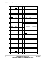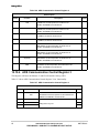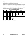
1
ADS Board Specification
MPC8560/ADS8540/D
Rev. 0.5.1, 6/2004
MPC8560/MPC8540 ADS
Specification
MPC8560/MPC8540
Power QUICC IIITM
Integrated Communications
Processor ADS Board Specification
PRELIMINARY—SUBJECT TO CHANGE WITHOUT NOTICE
Documentation History
2
Date
Author
Version
Comments
7/1/2002
V. Yukht
1.0
Initial Draft in Word (Chapters 1 - 10)
7/1/2002
H. Amir
1.0
Initial Draft in Word (Chapters 11 - 13)
10/14/2002
D. I. Forsyth
0.2
Edited in Framemaker for customer release
10/16/2003
H. Amir
1.3
Updated Version in Word
10/27/2003
D.I. Forsyth
0.3
Edited in Framemaker for customer release
includes Pilot updates.
11/10/03
D.I. Forsyth
0.4
Edited changes in tables of contents.
2/5/04
D.I. Forsyth
0.5
Incorporate update from V. Yukht.
4/5/2004
RG
0.5.1
6/4/2004
RG
0.6
Updated Fig. 12-4, 12-5; updated text in Section 12.6
Updated Fig. 10-1, 11-2, Table 11-1, 12-1; added
Table 11-4, 11-5
MPC8560/MPC8540 ADS Specification
PRELIMINARY—SUBJECT TO CHANGE WITHOUT NOTICE
MOTOROLA
Table of Contents
Topic
Document History
Part I, “Introduction”
Section 1.1, “Document Objective”
Section 1.2, “The Role of ADS”
Section 1.3, “Reference Documents”
Part II, “MPC8560 and MPC8540 Features Overview”
Section 2.1, “MPC8560 Block Diagram”
Section 2.2, “MPC8540 Block Diagram”
Section 2.3, “MPC8560/MPC8540 ADS Block Diagram”
Section 2.4, “Reference HIP Expansion Card”
Section 2.5, “Reference ADS Component Placement”
Part III, “DDR SDRAM Interface”
Section 3.1, “DDR Interface Overview”
Section 3.2, “Power for DDR”
Section 3.3, “Synchronization”
Section 3.4, “Serial Presence Detect (SPD) Function”
Section 3.5, “Debug Function”
Part IV, “RapidIO Interface”
Section 4.1, “RapidIO Interface Overview”
Section 4.2, “Power for RapidIO”
Section 4.3, “Placement of RapidIO Connectors”
Part V, “Power Supply”
Section 5.1, “Primary Power Supply”
Section 5.2, “ADS Power Supply Structure”
Section 5.3, “Power Supply Operation”
Part VI, “PCI/PCI-X Interface”
Section 6.1, “PCI/PCI-X Overview”
Section 6.2, “Auto Identification”
Section 6.3, “PCI/PCI-X Clocking”
Section 6.4, “PCI/PCI-X Reset”
Section 6.5, “Optional JTAG Connectivity”
Section 6.6, “PCI/PCI-X Power”
Section 6.7, “PCI/PCI-X Interrupts”
Section 6.8, “PCI/PCI-X Control”
Section 6.9, “PCI Slot Connector Pinouts”
Page
2
5
5
5
5
6
7
8
8
9
9
10
10
11
11
11
11
12
12
13
13
15
16
16
17
20
21
21
21
21
21
21
21
22
22
MOTOROLA
MPC8560/MPC8540 ADS Specification
Part VII, “Clocking”
25
PRELIMINARY—SUBJECT TO CHANGE WITHOUT NOTICE
3
Section 7.1, “Clocking Architecture”
Section 7.2, “Clock Control”
Section 7.3, “Clock Out Parameters”
Part VIII, “JTAG Test Access Port (TAP)”
Section 8.1, “JTAG TAP Connection”
Part IX, “System Control and Debug Signals”
Section 9.1, “System Control”
Section 9.2, “Reset Configuration”
Section 9.3, “Debug Signals”
Part X, “ADS Reset unit”
Section 10.1, “Reset Overview”
Section 10.2, “Power-On and Hard Reset”
Section 10.3, “Soft Reset”
Section Part XI, “Triple Speed Ethernet Controller (TSEC) Interface”
Section 11.1, “TSEC Overview”
Section 11.2, “Physical Media Interfaces”
Section 11.3, “TSEC Host Interfaces”
Section 11.4, “Hardware Configuration”
Part XII, “CPM Interface”
Section 12.1, “Communication Ports”
Section 12.2, “ATM Ports”
Section 12.3, “Mode Selection”
Section 12.4, “Fast Ethernet (10/100 Base-T)”
Section 12.5, “Fast Ethernet Mode Selection”
Section 12.6, “RS-232 Ports”
Section 12.7, “Expansion Connectors”
Section 12.8, “TCOM/ECOM Add-in Board Connection”
Section 12.9, “ ADS Communication Control Registers”
Section 12.10, “Debug LED’s”
Part XIII, “Local Bus Interface”
Section 13.1, “Local Bus Features”
Section 13.2, “Address Latch/ Data Transceiver”
Section 13.3, “Zero Bus Turnaround (ZBT) SRAM”
Section 13.4, “SDRAM”
Section 13.5, “Local Bus and Flash”
Section 13.6, “Local Bus ATM PHYs and Control Logic”
Section 13.7, “Expansion Connector”
Section 13.8, “MPC8560/MPC8540 Clock Driver”
4
25
25
26
27
27
30
31
31
32
33
33
33
33
34
34
35
35
38
40
40
41
42
49
50
50
51
61
61
62
69
69
70
70
71
73
74
75
80
MPC8560/MPC8540 ADS Specification
PRELIMINARY—SUBJECT TO CHANGE WITHOUT NOTICE
MOTOROLA
Document Objective
Part I Introduction
1.1
Document Objective
This document defines a technical specification for the MPC8560/MPC8540 ADS; this development board
will be used to verify the operation of the MPC8560 and MPC8540 integrated communications processors.
1.2
The Role of ADS
The ADS helps to fill the void between the traditional design-focused, electrical, circuit, and logical testing
and actual customer applications. While the ADS cannot practically mimic every possible customer design,
it does provide exposure to issues associated with the simultaneous operation of various interfaces and
protocols that are most likely to be found in specific market applications.
In addition to verifying the simultaneous operation of interfaces and protocols, the ADS provides a level of
systems performance characterization that will prove useful to users.
To assist in system debugging, on board PCB compression land pattern connectors to the Tektronix
TLA7Axx Series Logic Analyzer Probes P6860/P6880 are provided.
1.3
•
•
•
•
•
•
•
•
Reference Documents
MPC8560 User’s Manual
MPC8560 Hardware Specification
MPC8540 User’s Manual
MPC8540 Hardware Specification
Elysium specification
8260 User’s Manual
8260 Web site
824x Web site
MOTOROLA
MPC8560/MPC8540 ADS Specification
PRELIMINARY—SUBJECT TO CHANGE WITHOUT NOTICE
5
Reference Documents
Part II MPC8560 and MPC8540 Features
Overview
The MPC8560 PowerQUICC IIITM, is the next generation integrated communications processor. The
MPC8560 comprises a communications processor module (CPM) that integrates many high-speed
communications interfaces and related protocols. In addition to the CPM, the MPC8560 also includes the
e500 high performance embedded core processor with 256 Kbytes of level-2 cache/SRAM. Coupled with
the CPM and the e500 are two triple speed Ethernet controllers (TSEC), a 64 bit PCI/PCI-X controller, a
RapidIO interface, and a DDR SDRAM memory controller.
The MPC8540 processor can be viewed as a subset of the MPC8560 device. The MPC8540 processor has
the same features as the MPC8560 processor except that in place of the CPM functionality, the MPC8540
has a DUART interface and a 10/100 Ethernet port for debugging.
The following list is an overview of the MPC8560/MPC8540 feature set.
MPC8560 and MPC8540:
•
•
•
•
•
•
•
•
•
•
•
Embedded e500 Book E compatible core running at 600–800 MHz
— 32 Kbyte data and 32 Kbyte instruction L1 caches
— 256 Kbytes of on-chip memory/L2 cache
One I2C controller
Two TSEC (Triple-Speed Ethernet Controller) supporting 10/100/1000 Mbps, MII, GMII, RGMII,
and TBI interfaces
DDR SDRAM memory controller
RapidIO interconnect supporting 8 bit mode, 2.5V LVDS at 500 MHz
PCI/PCI-X controller supporting PCI 2.2 and PCI-X 1.0 specifications
Local bus controller with 32-bit address and data at 167 MHz, three UPMs (user programmable
machines), SDRAM controller, GPCM (general purpose chip select machine), and eight
chip-selects
DMA controller
Programmable Interrupt Controller (PIC)
Boot sequencer for I2C interface to serial ROM
JTAG boundary scan interface
MPC8560-only:
•
6
RISC CPM running up to 333 MHz (1 Gbps aggregate bandwidth)
— 32 Kbytes of dual port RAM
— 128 Kbytes of ROM and 32 Kbytes of instruction RAM
— Two Utopia Level II multi-phy, master/slave ports (one at 16 bit)
— Three MIIs (media independent interfaces)
— Eight TDM (time division multiplexed) interfaces, supporting T1/E1, T3/E3, ISDN, IDL,
CEPT, GCI, PCM.
— Three FCCs (fast communications controllers) supporting up to 155 Mbps ATM, 10/100 Mbps
Ethernet, 45 Mbps HDLC.
MPC8560/MPC8540 ADS Specification
PRELIMINARY—SUBJECT TO CHANGE WITHOUT NOTICE
MOTOROLA
MPC8560 Block Diagram
— Two MCCs (multi-channel controllers) supporting 128 serial, full-duplex 64Kbps channels
— Four SCCs (serial communications controllers) supporting HDLC, UART, BISYNC.
— One SPI (Serial Peripheral Interface)
2.1
MPC8560 Block Diagram
DDR
SDRAM
I2C Controller
I2C
e500 Core
ROM,
SDRAM,
GPIO
Local Bus Controller
IRQs
Programmable
Interrupt Controller
CPM
MCC
MCC
Time Slot Assigner
FCC
Time Slot Assigner
I/Os
Serial Interfaces
MIIs
TC - Layer
UTOPIAs
TDMs
256 KB
L2 Cache/SRAM
DDR SDRAM Controller
FCC
FCC
SCC
SCC
Serial
DMA
ROM
32 KB L1
I Cache
32 KB L1
D Cache
Core Complex Bus
OCeaN
RapidIO Controller
RapidIO-8
16 Gb/s
PCI/PCI-X Controller
PCI-X 64b
133MHz
I-Memory
DMA Controller
DPRAM
SCC
RISC
Engine
SCC
Parallel I/O
SPI
Baud Rate
Generators
I2C
e500
Coherency
Module
10/100/1000 MAC
MII/GMII/TBI/
RTBI/RGMII
10/100/1000 MAC
Timers
CPM
Interrupt
Controller
Figure 2-1. MPC8560 Block Diagram
MOTOROLA
MPC8560/MPC8540 ADS Specification
PRELIMINARY—SUBJECT TO CHANGE WITHOUT NOTICE
7
MPC8540 Block Diagram
2.2
MPC8540 Block Diagram
DDR
SDRAM
256 KB
L2 Cache/SRAM
DDR SDRAM Controller
I2C
I2C Controller
e500 Core
ROM,
SDRAM,
GPIO
Local Bus Controller
IRQs
Programmable
Interrupt Controller
10/100
ENET
MIIs
Serial
e500
Coherency
Module
32 KB L1
I Cache
32 KB L1
D Cache
Core Complex Bus
OCeaN
RapidIO Controller
RapidIO-8
16 Gb/s
PCI/PCI-X Controller
PCI-X 64b
133MHz
DUART
DMA Controller
10/100/1000 MAC
MII/GMII/TBI/
RTBI/RGMII
10/100/1000 MAC
Figure 2-2. Block
2.3
Diagram of the MPC8540
MPC8560/MPC8540 ADS Block Diagram
The MPC8560/MPC8540 ADS is represented in Figure 2-3.
TSEC
interface
DDR
SDRAM
interface
PCI/PCI-X
interface
CPM
interface
(10/100/1000)
RapidIO
interface
Control,
Boot and
Debugging
Reset
Power
supply
MPC8540/
MPC8560
device
Local bus
interface
Socket
Clocking
JTAG TAP
ORCN
I2C Boot
EEPROM
DUART
10/100 ENET
Figure 2-3. MPC8560/MPC8540 ADS Block Diagram
8
MPC8560/MPC8540 ADS Specification
PRELIMINARY—SUBJECT TO CHANGE WITHOUT NOTICE
MOTOROLA
Reference HIP Expansion Card
Each interface module shown in the picture is described and detailed below.
2.4
Reference HIP Expansion Card
3.3V 64-bit
PCI
(optional)
Standard
PCI I/O
capabilities
Arrangement of
power and
alignment pin keys
for parallel or
serial RapidIO
8LP/EP
or
1x/4x
RapidIO
Power
Keys
Figure 2-4. HIP Expansion Card Format
Reference ADS Component Placement
Slot 1
Slot 0
PCI/PCI-X
Slot 2
HMZd
PCI-64
PCI-64
Slot 3
PCI-64
2.5
I/O area and PS
Area used for
MPC8560 processor,
DDR, including DDR PS,
and other components
CPM
Interfaces
TSEC
Interfaces
HIP card
fills two
PCI/ISA
Figure 2-5. ADS Component Placement
MOTOROLA
MPC8560/MPC8540 ADS Specification
PRELIMINARY—SUBJECT TO CHANGE WITHOUT NOTICE
9
DDR Interface Overview
Part III DDR SDRAM Interface
A detailed block diagram of the DDR SDRAM interface is represented in Figure 3-1.
DDR bus up to 166MHz
MPC8560
DDR
SDRAM
memory
interface
RS
DQ[0:63]
64
RT
RS
ECC[0:7]
8
RT
RS
WE~
1
RT
RS
RAS
1
RT
RS
CAS
1
RT
RS
CS[0:1]
2
RT
RS
CS[2:3]
2
RT
RS
CKE[0:1]
2
RT
RS
DQS[0:8]
9
RT
RS
I2C(SDA,SCL) 2
RS
I2C[SA0:SA2]
3
RS
DM[0:8]
9
184 pin
DDR, ECC
and SPD
DIMM
Socket 1
[64:512MB]
184 pin
DDR, ECC
and SPD
DIMM
Socket 2
[64:512MB]
RT
MSYNC_OUT
MSYNC_IN
GVDD
DDR SDRAM
and RapidIO
bus supply
voltage
RS
MA[0:13]
14
RT
RS
BA[0:1]
2
RT
RS
CK[0:2]diff
6
RS
CK[3:5]diff
6
Not
Populated
VDD,VDDQ
DDR
termination
regulator
VREF
Termination
VTT
RS=22R
RT=51R
3.3V I2C
Figure 3-1. DDR Bus
3.1
DDR Interface Overview
The DDR SDRAM interface is implemented with a standard 184-pin DIMM sockets ready for operation
with one unbuffered DDR DIMM module inserted into them. This interface ensures ECC and SPD functions
of the DDR DIMM modules. The interface provides correct operation with DDR DIMM modules with a
clock rate up to 166MHz (333MHz—PC2100 DDR data rate). In order to guarantee this performance, an
appropriate layout should be used.
10
MPC8560/MPC8540 ADS Specification
PRELIMINARY—SUBJECT TO CHANGE WITHOUT NOTICE
MOTOROLA
Power for DDR
3.2
Power for DDR
Each DDR socket (DIMM module) and MPC8560 devices are powered by appropriate VCC and reference
voltages from the separated power supply (See Section 5.2, “ADS Power Supply Structure”). A
corresponding termination voltage is also provided. Each interface line is terminated through the
recommended resistor Rt = 51 Ohms. Optional serial termination resistors, Rs = 22 Ohms, are also
provided. Serial presence detect (SPD) Serial I2C EEPROM mounted in the DDR DIMM are powered from
the system 3.3V power source.
3.3
Synchronization
To ensure correct timing of the bus, the MSYNC_IN and MSYNC_OUT pins of the MPC8560 device are
connected to each other through a special conductor to provide the same propagation delay to all other
interface signals.
3.4
Serial Presence Detect (SPD) Function
The serial presence detect (SPD) function is implemented by connecting the DIMM I2C signals to the CPM
I2C interface of the device or (optionally) to the host PC through the appropriate parallel port.
The ADS is equipped with one unbuffered 128MByte PC2100 ECC SPD DIMM such as the
MT5VDDT1672AG-335C3 from Micron Co.
3.5
Debug Function
The optional debug function on the DDR SDRAM interface is provided by connecting ECC[0-4] signals
from MPC8560/MPC8540 device to the corresponding on-board logic analyzer connector through an
auxiliary switch. In this mode DDR SDRAM should operate without ECC functionality.
MOTOROLA
MPC8560/MPC8540 ADS Specification
PRELIMINARY—SUBJECT TO CHANGE WITHOUT NOTICE
11
RapidIO Interface Overview
Part IV RapidIO Interface
4.1
RapidIO Interface Overview
The RapidIO interface is implemented as a dual unidirectional 8-bit parallel bus connecting corresponding
MPC8560 device pins with the recommended HMZd RapidIO connector from AMP Co.
A detailed block diagram of the RapidIO (RIO) interface is represented in Figure 4-1.
RapidIO
Interface
Tek. LA
Compression
connectors
Guide pin
TCLK
A10
TCLK
TFRAME
TFRAME
TD[0:7]
TD[0:7]
RCLK
P6
RCLK
RFRAME
RFRAME
RD[0:7]
A1
RD[0:7]
3.3V
5.0V
P6
(top view)
GND
A
B
C
P8
A
B
C
P9
Guide pin
1
10
A
B
BG
C
D
DG
E
F
FG
G
H
HG
A
B
BG
C
D
DG
E
F
FG
G
H
HG
P6: P/N 1469002-2(Amp)
P8, P9: P/N 223955-2(Amp)
Guide pin: P/N 223956-1(Amp)
Figure 4-1. RapidIO Interface
12
MPC8560/MPC8540 ADS Specification
PRELIMINARY—SUBJECT TO CHANGE WITHOUT NOTICE
MOTOROLA
Power for RapidIO
4.2
Power for RapidIO
The RapidIO bus power is supplied through a pair of recommended connectors from AMP Co. All RapidIO
interface lines link up to logic analyzer probe heads with a compatible footprint to provide correct signal
measuring up to 500MHz.
4.3
Placement of RapidIO Connectors
RapidIO connectors are placed with PCI/PCI-X slot #0 to provide recommended HIP card insertion as
shown in Figure 4-2 and Figure 2-5.
The JN2 connector pin assignments are defined in Table 4-1.
Table 4-1. RapidIO Connector Assignments
Col
A
B
BG
C
D
DG
E
F
FG
G
H
HG
RFRAME RFRAME
1
TD0
TD0
2
TD1
TD1
RD7
RD7
3
TD2
TD2
TD6
RD6
4
TD3
TD3
TD5
RD5
5
TCLK0
TCLK0
TD4
RD4
RCLK0
RCLK0
GND
Not
Used
Not
Used
GND
Not
Used
Not
Used
GND
6
TD4
TD4
7
TD5
TD5
RD3
RD3
8
TD6
TD6
RD2
RD2
9
TD7
TD7
RD1
RD1
10
TFRAME TFRAME
RD0
RD0
GND
A HIP card dummy connection with mounted RapidIO and PCI/PCI-X connectors is shown in Figure 4-2.
13
MPC8560/MPC8540 ADS Specification
PRELIMINARY—SUBJECT TO CHANGE WITHOUT NOTICE
MOTOROLA
Placement of RapidIO Connectors
Figure 4-2. HIP Mechanical Sample
14
MPC8560/MPC8540 ADS Specification
PRELIMINARY—SUBJECT TO CHANGE WITHOUT NOTICE
MOTOROLA
Placement of RapidIO Connectors
Part V Power Supply
A detailed block diagram of the power supply distribution is shown in Figure 5-1.
LCORE
110/220AC
Dip
switches
LPLL
FAN5070
programmable
synchronous
DC/DC
controller
(step
25mV)
PWR_OK
PLD
Progr/manual
VID0
VID1
VID2
VID3
VID4
VID[0:4]
Control
register
& MUX
8-bit data
Control register WR
Control register RD
Control register CS
Extra LPF
AVDD
(1.05-1.825V
@0.1A)
VDD
(1.05-1.825V
@28A)
Core
PWR good1
Optional
ORCN
LDDR
5VDC power
PWR_OK
Dip switches
VID0
VID1
VID2
VID3
VID4
PLD
VID[0:4]
Control
register
& MUX
PWR good2
RC5051
programmable
synchronous
DC/DC
controller
(1.3-3.5V
step 25mV)
12VDC power
GVDD
(2.5V@6A)
FAN1654
1.5A LDO
bus
termination
regulator
VTT
([email protected]
VREF out
PWR_OK
Optional
VGETH
(3.3/2.5V
@3A)
LTSEC
5VDC power
SI4701 load switches
LT1764-3.3
linear
regulator
VGETH
(3.3V
@3A)
RIO(<=7A)
RIO(<=5A)
ATX
PS
300W
DDR
VTT sense
CPM(<=7A)
LT1764-2.5
linear
regulator
VGETH
(2.5V
@1A)
LT1764-1.5
linear
regulator
VGETH
(1.5V
@1A)
TSEC
Periphery
PCI(<=7A)
DMA/DUART/
I2C/INT/etc
(<=7A)
PWR good3
3.3VDC power
MAX934
comparator
Periphery
voltages
LBIU(<=7A)
PWR good4
PWR good5
PERIPHERY_ON
5VSB
On/OFF
PWR_OK
MXD1812
PS_RDY
reset
control
Start
WatchDog
10mS
T
One
PWR_ shot
ON_
RST
PWR_ON_RST
Flip
flop
Delay
~1mS
STOP
RST
PWR_ON_RST
S
Flip
flop
PWR_FAILED
RST
Progr PWR_OFF
WD PWR_OFF
PS_ON
PWR good1
PWR good2
PWR good3
PWR good4
PWR good5
PWR_ON
Figure 5-1. Power Supply Block Diagram
15
MPC8560/MPC8540 ADS Specification
PRELIMINARY—SUBJECT TO CHANGE WITHOUT NOTICE
MOTOROLA
Primary Power Supply
The ADS power supply provides all necessary voltages for correct operation of the MPC8560 device and
all on-board periphery.
5.1
Primary Power Supply
A standard CE/UL-approved PC ATX 400W power supply is used as the primary power supply. The ATX
power supply produces all power required by the MPC8560 device and other ADS components through the
following parameters:
•
•
•
•
•
•
•
•
5.2
Vin = 90–265V AC
Nin freq. = 47–63 Hz
Iin < 7A
Combined Power 220W max
— 3.3V DCout±5% @ 0.3–28A
— 5V DCout±5% @ 30A
12V DCout±5% @ 15A
-12V DCout±10% @ 0.8A
-5V DC @±10% @ 0.3A
5V DCsb±5% @ 0.72A
ADS Power Supply Structure
The ADS power supply consists of the following:
•
•
•
•
•
•
•
16
Programmable synchronous DC/DC converter
— Based on FAN5070 controller from Fairchild Co. to produce MPC8560 device core/PLL
voltages
— (VDD 1.05-1.825V with step 25mV, Rated Voltage 1.2V, Iout <=28A)
Programmable synchronous DC/DC converter
— Based on RC5051 controller from Fairchild Co. to produce DDR SDRAM voltages
— (GVDD 1.3-3.5V with step 25mV, Rated Voltage 2.5V, Iout <=6A)
LDO regulator (FAN1654 Fairchild Co.)
— Produces DDR bus required termination and reference voltages
— (VTT, = 1.25V @1.5A, VREF = 1.25V)
Set linear regulators (LT1764-3.3, LT1764-2.5, LT1764-1.5 from Linear Tech.)
— Provides all necessary TSEC PHY’s and corresponding MPC8560 device voltages
— (3.3V DC @3A, 2.5V DC @1A, 1.5V DC @1A)
Multi-channel voltage comparator (MAX934 from Dallas-Maxim Co.)
— Determines power good status of the TSEC supply voltages
Set power load switches
— Realizes 5V and 3.3V on/off function on the ADS.
— (Si4701 from Vishay Co. Icomm <= 7A)
Control circuits
— Provides necessary power on/off, visual indication, and power sequence functions.
MPC8560/MPC8540 ADS Specification
PRELIMINARY—SUBJECT TO CHANGE WITHOUT NOTICE
MOTOROLA
Power Supply Operation
5.3
5.3.1
Power Supply Operation
Power-On
The ATX power supply provides 5VSB (5V Standby) voltage immediately after connection to an AC power
outlet. This voltage powers the control circuits of the on-board power supply as follows:
•
•
•
•
•
•
5.3.2
•
5.3.3
After the 5VSB appears, the auxiliary reset controller (MXD1812 from Dallas-Maxim Co.)
produces a reset signal to reset the Power-On/Off flip-flop and the Power Failed flip-flop. The
yellow LED “PS Ready” indicates the ready status of the PS to operate. No other voltages are
present on the board.
When the operator pushes the “On/Off” button, the Power-On/Off flip-flop sends PS_ON signal to
the ATX PS. The ATX PS produces all above-mentioned voltages and after finishing all transients,
produces the PWR_OK signal to inform the ADS that all output voltages are in good condition.
The PWR_OK signal is driven to the core and DDR DC/DC converters and the delay line.
Core and DDR voltages are produced with the same profile after about 1mS and the delay line
output Periphery_ON signal, switches on the TSEC regulators (Ton<10uS) and load switches (Ton<
50uS) to supply voltages to all other on-board periphery such as RapidIO, PCI etc.
Concurrently the WatchDog circuits start (T~10mS) to monitor the power-on condition.
In case of no failure, the Power Good signals from each supply stop the WatchDog and illuminate
the green “PWR_ON” LED. Otherwise, the WatchDog sets the Power Failed flip-flop – indicated
by illumination of the red “PWR_Failed” LED, and resets the Power On/Off flip-flop. In effect, this
cancels the PS_ON signal to the ATX PS so the ATX PS is switched off. In this case, recurring
switching on is only possible after reconnection of the ATX PS to the AC outlet.
Power Off
If the ADS is in Power-On status (“PWR_ON” LED is illuminated) and the operator pushes the
On/Off button, the Power-On/Off flip-flop cancels the PS_ON signal to the ATX power supply (i.e.
switches it off).
Over-Current, Voltage, and Temperature Protection
Each of the regulators used in the on-board power supply (along with the ATX power supply) have
embedded over-current, voltage, and temperature protection. Power load switches are protected with fast
over current protection circuits.
5.3.4
Current Measurement
The ability to measure the amount of current consumed by each module (for example, the core, the DDR
block, etc.) is provided by measuring the voltage drop on the fixed series resistors in the corresponding
circuits.
17
MPC8560/MPC8540 ADS Specification
PRELIMINARY—SUBJECT TO CHANGE WITHOUT NOTICE
MOTOROLA
Power Supply Operation
5.3.5
Auxiliary Function
To provide the capability for various device testing and analysis, there are options to switch off Core and/or
DDR on board voltages by disconnecting hard-wired control jumpers in the corresponding circuit.
5.3.6
Voltage Regulation
5.3.6.1
Core and PLL voltages
There are two ways to adjust VDD and AVDD voltages (simultaneously) within the stated-above limits:
•
•
Manually, by setting corresponding DIP switches (Progr./Manual switch in Manual position)
Remotely, by the Optional Remote Control Network (ORCN) through the Host PC parallel port
interface (Progr./Manual switch in Progr. position).
After power-on, these voltages are set to default values.
5.3.6.2
DDR Voltages
The DDR SDRAM GVDD and termination (VTT) and reference (VREF) voltages can be adjusted
automatically within the limits stated previously by manually setting corresponding DIP switches to desired
values. Note that the VOUT of the RC5051 goes to the GVDD of the DDR SDRAM.
After power-on, these voltages are set to default values.
5.3.6.3
TSEC Voltages
The voltage for the MPC8560 device TSEC interface pins can be switched to 3.3V or 2.5V, selected with a
jumper.
5.3.6.4
Power Sequence
Figure 5-2 summarizes the power sequence of the power supply.
18
MPC8560/MPC8540 ADS Specification
PRELIMINARY—SUBJECT TO CHANGE WITHOUT NOTICE
MOTOROLA
Power Supply Operation
PWR_IN
5VSB
ON/OFF
Pwr off
Pwr on
PS_ON
3.3VDC PWR,
5VDC PWR,
12VDC PWR
PWR_OK
VDD, AVDD
GVDD, VTT
PERIPHERY_ON
VTSEC
VRIO, VCPM,
VPCI, VLBU,
VDMA, etc.
WatchDog
Start WD
Release WD
WD expired
PWR_ON
1mS
WD interval ~10mS
Non-simultaneous power sequence <=0.5mS
Figure 5-2. Power Supply Sequence
19
MPC8560/MPC8540 ADS Specification
PRELIMINARY—SUBJECT TO CHANGE WITHOUT NOTICE
MOTOROLA
Power Supply Operation
Part VI PCI/PCI-X Interface
Figure 6-1 represents a detailed PCI/PCI-X interface block diagram.
PCI/PCI-X-64
Bus switches
slot #0
IDTQS34XVH245
PCI-64
slot #1
PCI-64
slot #2
PCI-64
slot #3
PCI_AD[0:63]
PCI_C_BE[0:7]
MPC8560
PCI/PCI-X
interface
PCI_PAR
PCI_PAR64
PCI_FRAME
PCI_TRDY
PCI_IRDY
PCI_STOP
PCI_DEVSEL
PCI_IDSEL
PCI_REQ64
PCI_ACK64
PCI_PERR
PCI_SERR
PCI_FRAME
PCI_REQ0
PCI_REQ1
PCI_REQ2
PCI_REQ3
PCI_REQ4
PCI_GNT0
PCI_GNT1
PCI_GNT2
PCI_GNT3
PCI_GNT4
TP
TP
PCI_INTA
PCI_INTB
PCI_INTC
PCI_INTD
PCI_CLK0
2
PCI_JTAG
connector
(optional)
PCI_CLK1
PCIslots
On/Off
PRSNT1,2
PCI_RST0
8
6
RST1
PCI_CLK2
PCI_CLK3
4
2
RST2
RST3
TDI
TDO
TCK
TMS
TRST
5.0V, +12V, –12V
3.3V PCI
PCI-X_CAP
JTAG2
To board
control
register
PCI_JTAG Select
PCI-X_CAP
JTAG3
JTAG4
M66EN
All Slots
PCI/PCI-X-66/PCI-X-133 add-in card detection and
PCI mode control logic
PCI-X-133
PCI-X-66
PCI
Figure 6-1. PCI/PCI-X Interface Block Diagram
20
MPC8560/MPC8540 ADS Specification
PRELIMINARY—SUBJECT TO CHANGE WITHOUT NOTICE
MOTOROLA
PCI/PCI-X Overview
6.1
PCI/PCI-X Overview
The combined PCI/PCI-X interface provides a standard interface to the MPC8560 device for PCI32/64
add-in cards operating at up to 66 MHz as well as PCI-X32/64 add-in cards operating at up to 133 MHz.
As shown in the block diagram, the interface consists of four standard 1.27 mm 184-pin 3V edge card
connectors (for example the 891779230 from Molex).
The nearest slot to the MPC8560 device (slot #0) is specified to operate in PCI/PCI-X modes while slots
#1–3 are for PCI cards only.
Bus switches, IDTQS34XVH245; 32 bit, Tpd = 250ps, Ron = 4R, from IDT Co. causes the PCI slots to be
disconnected from the bus in the case where the a PCI-X card is inserted into slot #0. This guarantees
optimal parameters of transmission on the high-frequency bus.
6.2
Auto Identification
Static auto identification mechanism provides recognition of the type of card inserted into a slot
(conventional PCI, PCI-X 66 MHz or PCI-X 133 MHz). Therefore, the bus switches mentioned above
should be turned either on or off. A three-level comparator are used for this detection. The signals to be
analyzed are PCIX_CAP from slot #0 and PCIX_CAP signals from slots #1–3.The signal from slot #0 has
the highest priority, so if a PCI-X card is inserted into slot #0, the conventional PCI slots #1–3 will be
disconnected from the bus.
6.3
PCI/PCI-X Clocking
Each slot is clocked with individual clock signals from the system clock distribution buffer, as
recommended by the PCI/PCI-X standard, to provide the same clock timing parameters.
6.4
PCI/PCI-X Reset
Each slot receives a common PCI_Reset signal as recommended by the PCI/PCI-X standard.
6.5
Optional JTAG Connectivity
All PCI/PCI-X slots are connected to the optional JTAG connector, as specified in the standard, to provide
appropriate add-in card service (if required).
6.6
PCI/PCI-X Power
All PCI/PCI-X slots are powered with appropriate voltages from the on-board power supply as specified by
the PCI/PCI-X standard.
6.7
PCI/PCI-X Interrupts
The PCI/PCI-X interrupt signals are connected to the suitable MPC8560 device EPIC inputs in compliance
with a standard provided order.
The PCI/PCI-X interrupt routing is represented in Table 6-1.
21
MPC8560/MPC8540 ADS Specification
PRELIMINARY—SUBJECT TO CHANGE WITHOUT NOTICE
MOTOROLA
PCI/PCI-X Control
Table 6-1. PCI/PCI-X Interrupts
PCI/PCI-X Slot #0
MPC8560
INT#
1
Int
A
Int
B
Int
C
PCI Slot #1
Int
D
Int
A
Int
B
Int
C
*
2
PCI Slot #2
Int
D
Int
A
Int
B
*
*
Int
C
Int
A
Int
B
*
*
Int
C
*
*
*
Int
D
*
*
*
4
Int
D
*
*
3
PCI Slot #3
*
*
*
Note: * - means “connection”
6.8
PCI/PCI-X Control
To facilitate and simplify operation with the PCI/PCI-X interface, additional control logic provides visual
inserted add-in card type indication and read/write capability (status) of the inserted add-in cards through
the Board Control Register (Local Bus mapped) as follows:
•
•
•
•
•
Identification of the inserted add-in card is reflected with two PCIXCAP signals (4 bits—Input)
Power Management Enable (PME) signal (1 bit—I/O)
66 MHz Enable – M66EN signal (1 bit—Input)
Present—Prsnt1, 2 signals (8 bit—Input)
Bus switches (connection Slots#1-3 to the PCI bus) status—On/Off (1 bit—I/O)
A bit map of the corresponding control register is shown in Table 6-2.
Table 6-2. PCI/PCI-X Control Register Map
MSB
0
Bit Numbers
1
Slot #0
PCIXCAP
2
3
Slots#1-3
PCICAP
4
5
6
7
8
9
LSB
10
11
Slot#0,
Prsnt
Slot#1,
Prsnt
Slot#2,
Prsnt
Slot#3,
Prsnt
1
1
1
1
2
2
2
2
12
13
14
15
M66
EN
Bus
switch
On/Off
NU
NU
See Part XIII, “Local Bus Interface”, for detailed descriptions of the corresponding Board Control Register
bits.
6.9
PCI Slot Connector Pinouts
The PCI/PCI-X 64bit connector pinout for 3.3V system environment is shown in Table 6-3.
22
MPC8560/MPC8540 ADS Specification
PRELIMINARY—SUBJECT TO CHANGE WITHOUT NOTICE
MOTOROLA
PCI Slot Connector Pinouts
Table 6-3. PCI/PCI-X Connector Pinout
PIN
Side B
Side A
Comments PIN
Side B
Side A
1
-12V
TRST
49
M66EN (PU)
AD9
2
TCK
+12V
50
GND
GND
3
GND
TMS
51
GND
GND
4
TDO
TDI
52
AD8
C_BE0
5
+5V
+5V
53
AD7
+3.3V
6
+5V
INT A
54
+3.3V
AD6
7
INT B
INT C
55
AD5
AD4
8
INT D
+5V
56
AD3
GND
9
PRSNT1
Reserved
57
GND
AD2
10 Reserved
+3.3V(I/O)
58
AD1
AD0
11
Reserved
59
+3.3V(I/O)
+3.3V(I/O)
60
ACK64
REQ64
61
+5V
+5V
62
+5V
+5V
12
PRSNT2
Connector key
13
14 Reserved
15
GND
RST-
16
CLK
+3.3V(I/O)
17
GND
GNT
63
Reserved
GND
18
REQ
GND
64
GND
C_BE7
PME- (PU)
65
C_BE6
C_BE5
19 +3.3V(I/O)
23
3.3V Aux
3.3V Key
Connector key
20
AD31
AD30
66
C_BE4
+3.3V(I/O)
21
AD29
+3.3V
67
GND
PAR64
22
GND
AD28
68
AD63
AD62
23
AD27
AD26
69
AD61
GND
24
AD25
GND
70
+3.3V(I/O)
AD60
25
+3.3V
AD24
71
AD59
AD58
26
C_BE3
IDSEL
72
AD57
GND
27
AD23
+3.3V
73
GND
AD56
28
GND
AD22
74
AD55
AD54
29
AD21
AD20
75
AD53
+3.3V(I/O)
30
AD19
GND
76
GND
AD52
31
+3.3V
AD18
77
AD51
AD50
32
AD17
AD16
78
AD49
GND
33
C_BE2
+3.3V
79
+3.3V(I/O)
AD48
34
GND
FRAME
80
AD47
AD46
35
IRDY
GND
81
AD45
GND
Comments
64-Bit Spacer
MPC8560/MPC8540 ADS Specification
PRELIMINARY—SUBJECT TO CHANGE WITHOUT NOTICE
MOTOROLA
PCI Slot Connector Pinouts
Table 6-3. PCI/PCI-X Connector Pinout (continued)
24
PIN
Side B
Side A
Comments PIN
Side B
Side A
36
+3.3V
TRDY
82
GND
AD44
37
DEVSEL
GND
83
AD43
AD42
38 PCIXCAP
STOP
84
AD41
+3.3V(I/O)
39
LOCK
+3.3V
85
GND
AD40
40
PERR
SMBCLK (PU)
Not used
86
AD39
AD38
41
+3.3V
SMBDAT (PU)
Not used
87
AD37
GND
42
SERR
GND
88
+3.3V(I/O)
AD36
43
+3.3V
PAR
89
AD35
AD34
44
C_BE1
AD15
90
AD33
GND
45
AD14
+3.3V
91
GND
AD32
46
GND
AD13
92
Reserved
Reserved
47
AD12
AD11
93
Reserved
GND
48
AD10
Gnd
94
GND
Reserved
Comments
Not used
MPC8560/MPC8540 ADS Specification
PRELIMINARY—SUBJECT TO CHANGE WITHOUT NOTICE
MOTOROLA
Clocking Architecture
Part VII Clocking
Figure 7-1 shows a detailed block diagram of the ADS clocking system.
ADS full version
MPC9239
ORCN
Ctrl Reg WR
Ctrl Reg RD
Ctrl Reg CS
PLD
16MHz
CLK_SEL
PECL
Dip switches
‘clock set’
M0
M6
N0,N1
PWD
Local/
remote
control
••
••
••
•
MPC8560
device
MPC9448
8-bit data
Clock
generator
control
register
and MUX
M[0:6],
N[0:1],
PWD
FOUT
FOUT
PCI_CLK0
PCI_CLK1
PCI_CLK2 PCI_CLK
PCI_CLK3
PCICntr.
Reset unit
PCI-LA.
SYSCLK
Fanout
buffer
FOUT<=
350MHz
External
generator
CLK
CCLK
Clock
synthesizer
FOUT=
3.12-900MHz
P_LOAD
Fixed
clock
generator
(optional)
External
RTC
generator
RTC
SET
Manual
RST
Remote
Figure 7-1. ADS Clocking System Block Diagram
7.1
Clocking Architecture
The clocking system must supply the required clock signals to the MPC8560 device and PCI/PCI-X add-in
cards.
To provide flexibility, the MPC9239 clock synthesizer device from Motorola is used. It supplies the ADS
with clock signals in the 3.125– 900MHz range. The output clock from the synthesizer (differential PECL)
comes to the MPC9448 fanout buffer from Motorola, which converts it to CMOS, and distributes it to the
MPC8560 device itself and to each PCI/PCI-X slot individually. Note the Fanout buffer has a maximum
frequency of 350MHz. It is possible to use an external clock generator instead, if the CLK SEL switch is set
to the appropriate position (“1”). To measure the clock, the clock signal test point should be used. A separate
external generator connector should be used to drive the RTC auxiliary input of the MPC8560 device.
7.2
Clock Control
The clock synthesizer has the capacity to program its output through an 10-bit parallel interface. The ADS
provides this function by either setting the DIP switches to the desired value or optionally, through the
Optional Remote Control Network (ORCN) [Part VIII of this document].
The default clock output value is defined by the DIP switches.
25
MPC8560/MPC8540 ADS Specification
PRELIMINARY—SUBJECT TO CHANGE WITHOUT NOTICE
MOTOROLA
Clock Out Parameters
7.3
Clock Out Parameters
Clock synthesizer produces the clock signals with a period jitter < ±25 pS as follows:
Output Frequency Range, MHz
Frequency Step, MHz
3.125-56.25
<1
50–112.5
2.0
100–225
4.0
200–450
8.0
The clock fan-out buffer supplies the clock signal to the MPC8560 device with following parameters:
•
•
•
•
26
Output clock frequency range 0–350 MHz
Clock skew < 150 pS
Each output drives one 50 Ohm parallel terminated transmission line or alternatively, a 50 Ohm
series terminated transmission line
Output rise/fall time 0.1–1 nS
MPC8560/MPC8540 ADS Specification
PRELIMINARY—SUBJECT TO CHANGE WITHOUT NOTICE
MOTOROLA
JTAG TAP Connection
Part VIII JTAG Test Access Port (TAP)
Including Connection, Optional Remote Control Network (ORCN), and I2C Boot EEPROM
A detailed block diagram of the ADS JTAG connection, ORCN, and I2C Boot is represented in Figure 8-1.
74LVX161284
(Fairchild)
Parallel
port
Altera
(Series 3000)
SN74LVT8980
(TI)
A[0:3]
Address
latch,
decoder
and I2C
transceiver
Voltage
Transceiver
JTAG
TAP
master
D[0:8]
Control
JTAG
JTAG
signals
JTAG
bus
F.oper
<=30MHz JTAG
signals
JTAG
1
2
3
Mode
BootWiz
PLD
8-bit data
Control register WR
JTAG-EPP
Control register RD
JTAG-Serial
Control register CS
ORCN
to PS and
CLK
generator
MPC8560
Device
JTAG-Ext. Conv
I2C-PP
ADS full version
(optional)
I2c-CPU
SCHMOO
Socket
Jumper
SCL,
SDA
256Kbit
serial
EEPROM
Write
protect
SCL, SDA
I2C
FM24C256FLN
(Fairchild)
SCL
SDA
Figure 8-1. DC JTAG TAP, ORCN and I2C Boot Block Diagram
8.1
JTAG TAP Connection
The MPC8560 device JTAG connection capability is provide in the following two ways:
•
27
Direct connection to the appropriate header connector
MPC8560/MPC8540 ADS Specification
PRELIMINARY—SUBJECT TO CHANGE WITHOUT NOTICE
MOTOROLA
JTAG TAP Connection
•
Optional Host PC Parallel Port connection
8.1.1
JTAG Header
The JTAG header provides connection between the MPC8560 device and any external compatible JTAG
converter such as a Wiggler or probes for example, AMC WireTAP.
The JTAG dual-in-row header pin-out is represented in Table 8-1.
Table 8-1. JTAG Header Pinout
Pin Number
1
2
3
4
5
TDO Not TDI TRST PU-10k
used
#
0Vdd
8.1.2
6
7
8
9
10
11
12
13
14
15
16
VDD_
TCK CHKSTP TMS NC SRST NC HRST Key CHKSTP GND
SENSE
_IN#
#
#
_OUT#
connected
to 3V3DC
Parallel Port Connection
The optional JTAG parallel port connection can provide two alternative functions:
1. The on-board JTAG converter (substitutes the external converter)– needs no host program
adaptation; it operates as if external JTAG converter is connected to the Host PC Parallel Port
2. Fast download mode. In this mode, the JTAG connection between the MPC8560 device and the
host PC operates with the on-board JTAG TAP Master Controller (SN74LVT8980 from TI), to
exchange data through the Host PC Parallel Port. Extra logic such as address latches, decoders,
etc., is implemented in a PLD from Altera. This option loads data to the MPC8560 device
approximately10 times faster than with the conventional JTAG converter (TCK up to 30 MHz).
However, this option requires adaptation of the Host PC drivers. HOST MODE switch block
possible position represented in the following table:
Table 8-2. Host Mode Switch Options
HOST MODE Switch
0
1
2
MODE
0
0
0
I2C-EPP
1
0
0
JTAG-PP (Serial)
0
1
0
JTAG-External Converter
1
1
0
JTAG-EPP (Parallel)
0
0
1
SHMOO (JTAG-Ext. Converter, Control-EPP
X
X
1
Reserved
6 LEDs indicate the current JTAG mode connection:
•
•
•
28
JTAG-EPP Parallel mode (Green)
JTAG-Serial mode (Red)
JTAG External Converter (Yellow)
MPC8560/MPC8540 ADS Specification
PRELIMINARY—SUBJECT TO CHANGE WITHOUT NOTICE
MOTOROLA
JTAG TAP Connection
•
•
•
8.1.3
I2C-PP (Programming serial Boot ROM through Host Parallel Port) (Red)
I2C-CPU (Normal mode serial Boot ROM connected to the CPU) (Green)
SHMOO (JTAG-External Converter, System Clock and Core voltage control through ORCN)
ORCN
The optional remote control network (ORCN) is used for the following functions:
•
•
MPC8560 core/PLL voltage program remote control
System clock synthesizer program remote control
To implement this control, an appropriate Host PC application program and drivers must be developed. On
the ADS, necessary hardware that constitutes the address decoder, set registers, etc. is developed in the same
PLD.
8.1.4
•
•
•
29
I2C Boot EEPROM
The MPC8560 device needs to be booted from external ROM through the serial I2C interface. As
recommended, a serial EEPROM FM24C256FLN from Fairchild Co. is used. This standard 256
Kbit device is organized as 32K x 8. It has write protection capability of its memory map. This part
fits into the socket to provide its reprogramming capability to an external programmer.
Visual status of the SCL and SDA lines is provided with corresponding Red and Green LED’s.
Optional connection to the Host PC through the same PLD provides the capability to reprogram the
on-board boot EEPROM.
MPC8560/MPC8540 ADS Specification
PRELIMINARY—SUBJECT TO CHANGE WITHOUT NOTICE
MOTOROLA
JTAG TAP Connection
Part IX System Control and Debug
Signals
A detailed block diagram of the ADS system control and debug signals is shown in Figure 9-1.
Debugging
Probe
head
footprints
MPC8560
device
Dip
switches
‘PCI
setting’
Debug
TP
MDVAL
TRIG_IN
TRIG_OUT
TRIG_OUT
Dip
switches
‘PLL, LB,
CLK & boot
setting’
TRI
MPC8560
device
PCI part
TRI
Local bus
PLD
Default
signal
status
register and
multiplexer
Core PLL ratio 0
Core PLL ratio 1
Sys
Sys PLL ratio 1
Sys PLL ratio 2
MSRCID[0:4]
TP
TP
TP
PCI I/O impedance
PCI I/O arbiter EN
PCI debug EN
PCI Width EN
Boot ROM location 0
Boot ROM location 1
Boot ROM location 2
LB port
width 1
CPU boot hold off
SPARE
TP
TP
TP
TP
L1_TSTCLK
L2_TSTCLK
TEST_SEL
(Device)
TP
CHKSTP_IN
TP
TP
CHKSTO_OUT
‘ASLEEP’
Host agent config 0
Host agent config 1
RapidIO CLK source 0
RapidIO CLK source 1
LSSD_MODE_B
ASLEEP
(Pwr Mngm)
Dip
switches
‘debug
select’
Memory debug select
DDR debug select
0
3
Boot sequence config 0
Device ID[0:3]
Dip
switches
‘device
ID &
boot’
Memory
debug
select
4
7
Boot sequence config 1
Device ID[4:7]
Dip switch
‘reduced Gbit’
Reduced Gbit
Dip switch
‘mode’
Local control/default
TRI
DDR
debug EN
Debug
••
•
TRI
TSEC1
TRI
TSEC2,
Eth, MII
••
•
Delay
ADS_RESET
Figure 9-1. ADS System Control and Debug Signals Block Diagram
30
MPC8560/MPC8540 ADS Specification
PRELIMINARY—SUBJECT TO CHANGE WITHOUT NOTICE
MOTOROLA
System Control
9.1
System Control
The MPC8560 device must be configured at power-on. During this time, the system parameters of the
various interfaces such as PCI configuration, PLL setting, etc. must be defined. Therefore, the MPC8560
device reads the status of the corresponding reset configuration pins during reset.
9.2
Reset Configuration
Each reset configuration pin of the MPC8560 device must be connected to a corresponding TRI-state buffer,
supplying the appropriate setting during ADS_RESET (after a short delay) as well as to the basic periphery.
Each signal has the capacity to be set by a corresponding DIP switch (CONFIG switch in MANUAL
position) or to be sampled by default values from a pre-programmed PLD register (CONFIG switch in
Default position). Default configuration signals set are currently not implemented.
The alternative Mode setting functions of the MPC8560 device pins are shown in Table 9-1 through
Table 9-5.
Table 9-1. PCI, Ethernet, and Debug Blocks
PCI
Main
Function
GNT_B1
Eth MI
GNT_B2
GNT_B3
Arbiter
En
Debug
En
Reset Config
I/O
Setting
Impedance
Debug
GNT_B4 REQ_64B EC_MDC
PCIX
Capable
PCI64
En
Reduced
Gbit
MSRCID0
MSRCID1
Memory
DDR
Debug Select Debug Select
Table 9-2. TSEC1 Block
TSEC1
Main
Function
Reset Config
Setting
TXD4
TXD5
TXD6
TXD7
LGPL3 (Local Bus)
GTX_CLK
Device ID3
Device ID2
Device ID1
Device ID0
Boot sequence
Config 0
Configuration
Table 9-3. TSEC2 Block
TSEC2
Main function
Reset Config
Setting
TXD4
TXD5
TXD6
TXD7
LGPL5 (Local Bus)
GTX_CLK
Device
ID7
Device
ID6
Device
ID5
Device
ID4
Boot sequence
Config 1
Configuration
Table 9-4. Local Bus Part 1
Main
Function
LB
LA27
LCS_B0
LCS_B1
LCS_B2
LCS_B3
Reset Config
CPU Boot Boot ROM Boot ROM Boot ROM LB Hold
Setting
Configuration Location 0 Location 1 Location 2 Enable 0
31
LCSB4
LB Hold
Enable 1
MPC8560/MPC8540 ADS Specification
PRELIMINARY—SUBJECT TO CHANGE WITHOUT NOTICE
MOTOROLA
Debug Signals
Table 9-5. Local Bus Part 2
Main
Function
Reset
Config
Setting
9.3
LB
LWE_B0
LWE_B1
LWE_B2
LWE_B3
LBCTL
LALE
LGPL0 LGPL1
PCI Hold
PCI Hold Host Agent Host Agent Reserved Core PLL RIO
Configuration Configuration
0
1
(Not used) ratio 0
clock 0
0
1
LGPL2
RIO Core PLL
clock 1 ratio 1
Debug Signals
To provide various ADS testing, dedicated pins of the MPC8560 device are connected to appropriate logic
analyzer on-board connector(s). Suitable test points are defined as shown in Figure 9-1.
32
MPC8560/MPC8540 ADS Specification
PRELIMINARY—SUBJECT TO CHANGE WITHOUT NOTICE
MOTOROLA
Reset Overview
Part X ADS Reset unit
A detailed block diagram of the ADS reset unit is shown in Figure 10-1.
PowerOn RESET
DS1834A
(Dallas-Maxim)
3.3VDC Pwr
One-shot
5VDC Pwr
RESET
controller
ADS RESET
OR
AND
Tpulse~
350mS
HRESET
≥10mS
HRESET
HRESET_REQ
MPC8560
device
One-shot
SRESET
≥10mS
SRESET
Figure 10-1. ADS Reset Unit Block Diagram
10.1 Reset Overview
The ADS reset unit resets the MPC8560 device itself as well as all periphery on-board components that
require reset. The reset unit provides power-on, hard-reset and soft-reset signals in compliance with the
MPC8560 hardware specification.
10.2 Power-On and Hard Reset
After the 5V DC and 3.3V DC input voltages are both stable, the DS1834A Dallas Semiconductor-Maxim
reset controller drives its 3.3V RST and 5V RST output signals low for approximately 350ms. Since the
system clock is running at 100KHz and the internal counter will wait 16,384 clock cycles to allow the PLL
to lock. The HRESET push button also provides manual reset control.
The HRESET push button starts a one-shot circuit with a debounce flip-flop, which produces a pulse to the
reset controller.
The output of the reset controller is AND’d with the HRESET_REQ output of the MPC8560 and routed to
the HRESET MPC8560 input. It provides a reset ‘start’ from Power-On or the HRESET push button and
‘stops’ it when the MPC8560 is ready to operate (auto canceling).
The soft reset signal is asserted at the same time as hard reset.
10.3 Soft Reset
The soft reset unit implements a one-shot circuit with a debounce flip-flop, which produce a pulse to the
SRESET input of the MPC8560. Tsrst ≥ 10mS, which is enough even if the system clock is 100kHz. (Tsrst
should be keep asserted for at least 1,024 clks).
33
MPC8560/MPC8540 ADS Specification
PRELIMINARY—SUBJECT TO CHANGE WITHOUT NOTICE
MOTOROLA
TSEC Overview
Part XI Triple Speed Ethernet Controller
(TSEC) Interface
11.1 TSEC Overview
Two Ethernet IEEE 802.3 ports with (10/100/1000-Base-TX) interface are provided on the ADS. Both of
the two ports have the ability (optionally) to connect to a fiber optic interface. Each one of the ports is able
to work with MII for 10/100-BaseT or GMII and TBI for 1000Base-T.
The 88E1011S transceiver device from Marvell is used for each of the MPC8560 10/100/1000 Ethernet
ports. The device configuration modes will be controlled via MDC MDIO signals.
The 88E1011S reset input is driven by the same HRESET signal which drives the MPC8560. This resets the
transceiver whenever a hard-reset sequence is taken. The 88E1011S may also be reset by asserting the
appropriate Reset G-Eth bit in the on-board Control Register (TSEC1 Register 2[0], TSEC2 Register 2[1])
Or by writing a one to bit 15 (MSB) of the 88E10011S control register (register 0), via the MDC and MDIO
(MII management) signals, which causes the PHY state machines to be reset. When the reset operation is
done, this bit is cleared to zero automatically. The reset occurs immediately.
The GMII pins pass through the logic analyzer connector to the 88E1011S PHY and a GMII connector. This
connector is defined later.
The 88E1011S is controlled via the MII management port, which is a two-wire interface consisting of a
clock (MDC) and a bi-directional data line (MDIO). This is in fact a bus, where up to 32 devices may reside
over it. This protocol defines a five-bit slave address field, which is compared against the slave address set
to each device by hardware during device reset, including the status of the appropriate five 88E1011S pins.
On the ADS, the slave addresses are hard-wired to b00000 for TSEC1 and b00001 for TSEC2. The
MPC8560 MDC MDIO pins are used also for the two 10/100Base-T, CPM and maintenance port.
The ADS TSEC interface is shown in Figure 11-1.
34
MPC8560/MPC8540 ADS Specification
PRELIMINARY—SUBJECT TO CHANGE WITHOUT NOTICE
MOTOROLA
Physical Media Interfaces
Fiber optic
transceiver
TSEC1EXP
MII/GMII/
TBI
TSEC1
Logic Analyzer
connector
PHY
88E1011S
Transformer
RJ45
connector
MDC MDIO
ADS communication control register
MPC8560
TSEC
interface
TSEC2
Logic Analyzer
connector
MII/GMII/
TBI
PHY
88E1011S
TSEC2EXP
Transformer
RJ45
connector
Fiber optic
transceiver
Figure 11-1. TSEC Block Diagram
The following shows the MAC interfaces between the MPC8560 and the 88E1011S.
11.2 Physical Media Interfaces
11.2.1
Copper Interface
The copper interface uses the 88E1011S MDI[3:0] +/- PHY pins that connects to the physical media for
1000Base-T, 100Base-T and 10Base-T modes of operation. These pins are connected through the
transformer to the UTP5 RJ45 connector.
11.2.2
Fiber
The fiber cable connects to the fiber optic transceiver. The fiber optic transceiver is connected via the serial
interface pins to the PHY device. The PHY device is then connected to the MPC8560 through the MII,
GMII, and TBI interfaces.
11.3 TSEC Host Interfaces
11.3.1
Gigabit Media Independent Interface (GMII/MII)
Table 11-1 indicates the signal mapping of the 88E1011S device to GMII/MII interface. The MII supports
100Base-T and 10Base-T modes by sharing pins of the GMII interface. This interface supports GMII to
35
MPC8560/MPC8540 ADS Specification
PRELIMINARY—SUBJECT TO CHANGE WITHOUT NOTICE
MOTOROLA
TSEC Host Interfaces
copper connections in all three speeds. The GMII-to-copper interface is selected by setting the 88E1011
HWCFG_MODE [3:0] to 0b1111. MDC MDIO will select the interface connection between MII, GMII and
TBI.
In 1000Base-T mode, the GMII interface is selected. A 125Mhz is supplied by one of the 88E1011 to the
MPC8540/60 from this clock the MPC8540/60 drives the 125Mhz clock to the second PHY’s GTX_CLK
pin. The T/RXDATA are 8 bits. In 100Base-T and 10Base-T modes, the selected interface is MII; in this
mode the TX_CLK is supplied by the PHY. In MII the T/RXDATA are 4 bits.
Table 11-1. Signal Mapping
GMII / MII PHY and Connector Pins
GMII/MII Signal Name
GMII
MII
Connector
GTX_CLK
GTX_CLK
—
GTX_CLK
TX_CLK
—
TX_CLK
TX_CLK
TX_ER
TX_ER
TX_ER
TX_ER
TX_EN
TX_EN
TX_EN
TX_EN
TXD[7:0]
TXD[7:0]
TXD[3:0]
TXD[7:0]
RX_CLK
RX_CLK
RX_CLK
RX_CLK
RX_ER
RX_ER
RX_ER
RX_ER
RX_DV
RX_DV
RX_DV
RX_DV
RXD[7:0]
RXD[7:0]
RXD[3:0]
RXD[7:0]
CRS
CRS
CRS
CRS
COL
COL
COL
COL
The GMII signal interconnections are represented in Figure 11-2.
MPC8560
TSEC
GMII mode
GTX_CLK
TX_ER
TX_EN
TXD[7:0]
RX_CLK
RX_ER
RX_DV
RXD[7:0]
CRS
COL
PHY
?
GTX_CLK
TX_ER
TX_EN
TXD[7:0]
RX_CLK
RX_ER
RX_DV
RXD[7:0]
CRS
COL
Figure 11-2. GMII Interconnections
11.3.2
Ten Bit Interface (TBI)
The TBI interface pin mapping is shown in Table 11-2. The TBI interface supports only 1000Base-T mode
of operation. The TBI-to-copper interface is selected by software through the MDC and MDIO pins.
36
MPC8560/MPC8540 ADS Specification
PRELIMINARY—SUBJECT TO CHANGE WITHOUT NOTICE
MOTOROLA
TSEC Host Interfaces
Table 11-2. TBI Signals
TBI Signal Names
TBI Signal Name
PHY Signal Name
TBI_TXCLK
GTX_CLK
RXCLK1
TX_CLK
TXD9
TX_ER
TXD8
TX_EN
TXD[7:0]
TXD[7:0]
RX_CLK0
RX_CLK
RXD9
RX_ER
RXD8
RX_DV
RXD[7:0]
RXD[7:0]
COMMA (see note)
CRS
Note: This pin should be connected to PU if used in TBI, in the PMC8540/60 side. In the ADS there
is a jumper that is unconnected in TBI MODE, by unconnecting it, it is automaticaly connected to
VCC by PU.
For TSEC1 it is J50
For TSEC2 it is J51.
As shown in Figure 11-3 below, the TBI uses the same GMII signals.
MPC8560
TSEC
PHY
TBI mode
TBI_TXCLK
GTX_CLK
RX_CLK1
TX_CLK
TXD9
TX_ER
TXD8
TX_EN
TXD[7:0]
TXD[7:0]
RX_CLK0
RX_CLK
RXD9
RX_ER
RXD8
Vcc
RX_DV
RXD[7:0]
RXD[7:0]
COMMA
CRS
Jumper
Figure 11-3. TBI Signal Diagram
11.3.3
Summary
Table 11-3 shows the MPC8560 device TSEC pins used for each of the above-mentioned interface modes.
37
MPC8560/MPC8540 ADS Specification
PRELIMINARY—SUBJECT TO CHANGE WITHOUT NOTICE
MOTOROLA
Hardware Configuration
Table 11-3. TSEC Pin Use
MAC Interface Pins
TSEC Pin Name
GMII
MII
TBI
GT_CLK
GT_CLK
—
TBI_TXCLK
TX_CLK
—
TX_CLK
RCLK1
TX_ER
TX_ER
TX_ER
TXD9
TX_EN
TX_EN
TX_EN
TXD8
TXD [7:0]
TXD [7:0]
TXD [3:0]
TXD [7:0]
RX_CLK
RX_CLK
RX_CLK
RXCLK0
RX_ER
RX_ER
RX_ER
RXD9
RX_DV
RX_DV
RX_DV
RXD8
RXD [7:0]
RXD [7:0]
RXD [3:0]
RXD [7:0]
CRS
CRS
CRS
COMMA
(see note)
COL
COL
COL
—
Note : In TBI remove the jumper.
J50 for TSEC1 J51 for TSEC2
11.4 Hardware Configuration
Configuration options like physical address, PHY operation mode, Auto-Negotiation, MDI crossover
(ENA_XC) and physical connection type are configured by the CONFIG [6:0] pins.
For G-Ethernet the TSEC PHYs get PHY addresses 0b00000 (TSEC1), and 0b00001 (TSEC2).
Note that the two 10/100Base-T already have the 0b00010, 0b00011 and (for the MPC8540 maintenance
port) 0b00011 (the same as for FCC3 Ethernet) addresses.
The default configurations of the TSEC1 PHY through J56 is shown in Table 11-4
Table 11-4. TSEC1 PHY Default Configuration
38
Connected to
J56 Pin
J56 Pin
Signal Name
Connected to
J56 Pin
16
2
3V3
9,11
TSEC1_CFG1
16
4
LED_TX
n/a
5
TSEC1_CFG2
6
6
LED_LINK10
5
7
TSEC1_CFG3
10
8
LED_LINK1000
n/a
9
TSEC1_CFG4
2
10
LED_RX
7
11
TSEC1_CFG5
2
12
LED_DPLX
n/a
13
TSEC1_CFG6
16
14
LED_LINK100
n/a
15
NC
n/a
16
GND
1,3,13
J56 Pin
Signal Name
1
TSEC1_CFG0
3
MPC8560/MPC8540 ADS Specification
PRELIMINARY—SUBJECT TO CHANGE WITHOUT NOTICE
MOTOROLA
Hardware Configuration
The default configurations of the TSEC2 PHY through J47 is shown in Table 11-5
Table 11-5. TSEC2 PHY Default Configuration
Connected to
J47 Pin
J47 Pin
Signal Name
Connected to
J47 Pin
4
2
3V3
5,9,11
TSEC1_CFG1
13,16
4
LED_TX
1
5
TSEC1_CFG2
2,9,11
6
LED_LINK10
n/a
7
TSEC1_CFG3
10
8
LED_LINK1000
n/a
9
TSEC1_CFG4
2,5,11
10
LED_RX
7
11
TSEC1_CFG5
2,5,9
12
LED_DPLX
n/a
13
TSEC1_CFG6
3,16
14
LED_LINK100
n/a
15
NC
n/a
16
GND
3,13
J47 Pin
Signal Name
1
TSEC1_CFG0
3
All the other options except the PHY address can change after reset using the MDC and MDIO signals.
The following are the PHY-selected modes of operation:
•
•
•
•
•
•
•
•
•
•
•
PHY address as mention above
Media Interface copper
Auto Negotiation, advertise all capability force Master for TESEC1 and prefer Master for TSEC2
Full duplex
Enable Crossover
Enable 125CL
GMII to copper
Disable fiber/ copper auto selection
Select MDC and MDIO interface
Interrupt polarity is active low
Termination resistance default to 50 ohm impedance for fiber
11.4.1
Mode Indication LEDs
Each TSEC PHY has 6 pins targeted for mode indication LEDs as follows:
•
•
•
•
•
•
LINK10Base-T
LINK100Base-T
LINK1000Base-T
DUPLEX
RXD
TXD
Each one of the LEDs can be turned on, off, or blinked by writing an appropriate bit into register 25, which
is the Manual LED override register of the corresponding PHY e.g. Marvell 88E1011S.
39
MPC8560/MPC8540 ADS Specification
PRELIMINARY—SUBJECT TO CHANGE WITHOUT NOTICE
MOTOROLA
Communication Ports
11.4.2
Fiber Optic and Magnetic
The transformer used is the PE5007 from Pulse Engineering. The transformer is connected to the RJ45
connector. The RJ45 connectors uses its 8 pins in 1000Base-T mode.
For the fiber optic interface, the HP HFBR-5710L device is used. The fiber optic transceiver is connected
directly to the gigabit Ethernet PHY.
Note that the fiber optic interface is not the default mode.
11.4.3
TSEC PHY Powering
The PHY devices require three power supplies: 3.3V DC, 2.5V DC, and 1.5V DC. Three corresponding
regulators on the board provide common power sources for both TSEC PHY#1 and PHY#2 (see Part V,
“Power Supply”).
Part XII CPM Interface
12.1 Communication Ports
The ADS includes several communication ports to allow convenient CPM evaluation. Obviously, it is not
possible to provide all types of communication interfaces supported by the CPM, but the ADS provides a
convenient connection to communication interface devices for the MPC8560 via the CPM expansion
connectors. These connectors reside at the edge of the board. In order to prevent long layout traces between
the CPM pins and their connection to the expansion connector, each CPM pin used on the board is
automatically disconnected from the expansion connector. All the CPM pins are connected to the logic
analyzer connectors. Figure 12-1 below shows the CPM pins connected through the logic analyzer
connector to the communication module and the expansion connector via the bus switch.
Bus switch
CPM
Communication
module
Logic
analyzer
Expansion
connector
Control
Figure 12-1. CPM Connection
The communication port interfaces provided on the ADS are listed below:
•
•
•
40
FCC1 ATM 155 MHz 16/8 bits Single or Multi-PHY/or an optional 622 MHz with 16 bits Single
PHY. ATM622 is via an adapter board it should be connected to the board for ATM622 uses.
FCC2 ATM 155 MHz with Utopia 8 bits or Ethernet 10/100Base-T.
FCC3 Ethernet 10/100Base-T, used also as a MPC8540 F-Ethernet maintenance port.
MPC8560/MPC8540 ADS Specification
PRELIMINARY—SUBJECT TO CHANGE WITHOUT NOTICE
MOTOROLA
ATM Ports
•
Two RS-232 ports residing on SCC1 and SCC2. SCC2 is also for MPC8540 internal DUART.
12.2 ATM Ports
To support the CPM ATM controller, there are two ATM ports on this board: two 155Mbps and connectors
for the 622Mbps add-in card. The 155Mbps ATM port can work either through Utopia 16 or 8 bits, and in
Multi or Single PHY Mode. The 622Mbps can operate Utopia 16 bit Single PHY Mode from the adapter.
PHY1 at 155Mbps ATM with Utopia interface is switched between FCC1 and FCC2. When it operates
through FCC1, it joins onto the Utopia Bus to PHY2 and PHY3 (622 Mbps and 155 Mbps).
PHY2 & PHY1 can be connected together for multiphy operation by SW4[4] or control register 0 [3] and
operate through FCC1 or FCC2. In this case, the Utopia bus connected from FCC2 is only 8 bits, or 8/16
bits when it is connected through FCC1. In any case, 622 Mbps is operating with Utopia 16 bits.
The 155 Mbps PHYs that are used are the PM5384 from PMC-SIERRA and the 622 Mbps PHY is the
PM5357 also from PMC -SIERRA. The physical interface for the ATM is optical, and from OCP, part
number TRP-03B. for the 622 Mbps and the HFBR-5805 for the 155 Mbps from Agilent are used. Two
40-pin connectors are used to fit the Adtech Utopia Pods. The connectors are connected as slaves. There are
several bus-switches to select between FCC1, FCC2, FCC3, SCC1 and SCC2 modes as follows:
•
•
•
•
•
Switch-2—Utopia 16 or 8 data bus (FCC1)
Switch-3—FCC1 connect or disconnect to RS232 and expansion connector
Switch-4—select FCC2 to Fast Ethernet 2 or PHY 1.
Switch-5—PHY1 join to PHY2 and PHY3 (FCC1)
Switch-7—select fast Ethernet 3 from CPM to the PHY or to the expansion connector. In MPC8540
mode it is automatically connected to Fast Ethernet which is connected to FCC3.
There are seven control registers called the ADS Communication Control Register 0-6 and jumpers that
select the destination for FCC1 and/or FCC2 and/or FCC3 connections.
Note: One jumper defines if the configuration will be through the programmable registers or by the external
switches.
The ATM PHY devices are controlled via the local bus (GPCM). The PHYs have address and data signals
that are connected through buffers. One chip select (CS3 and Addresses 20, 21, 22) signal with address
decoding selects one of the three ATM PHYs.
The three ATM PHYs receive their reset through reset bits [4:6] on the ADS Communication Control
Register #2 or from Hard Reset.
Also the three IRQ signals are connected together to the MPC8560 IRQ7 signal.
Figure 12-2 shows the CPM module block diagram. Note this is a representation of the logic and there are
some other switches detailed in Table 12-1 which are not detailed in the diagram.
41
MPC8560/MPC8540 ADS Specification
PRELIMINARY—SUBJECT TO CHANGE WITHOUT NOTICE
MOTOROLA
Mode Selection
ATM155
PHY1
ATM622
PHY2 Adapter
ATM155
PHY3
Address from local bus
Data from local bus
MII
Fast
Ethernet 2
FCC2
Bus switch #4
UTOPIA
ADS Communication
Control Registers
#5 Bus Switch
UTOPIA control signals
Logic
analyzer
CPM
Adtec
connector
UTOPIA8
UTOPIA16
FCC1
Bus Switch
#2
UTOPIA
Bus switch
Expansion
connector
#3
RS232-2
SCC2
MII
FCC3
Fast
Ethernet 3
Bus switch #7
Other
CPM
Signals
SCC1
RS232-1
Figure 12-2. CPM Connection Block Diagram
12.3 Mode Selection
The following tables and figures show each one of the bus switches represented in Figure 12-2. The
inputs of each one have CPM names and the outputs are the function names. Again please note that
Figure 12-2 is only a representation of the following signals. Specifically there are some switches
in this table not detailed in the Figure 12-2.
Table 12-1.
pin name
Function Name
Switch #
PA10
FCC1: RxD[0] UTOPIA 8 /
2 + 5 +3
PA10
FCC1: RxD[8] UTOPIA 16
2 +3
PA11
FCC1: RxD[1] UTOPIA 8 /
2 + 5 +3
PA11
FCC1: RxD[9] UTOPIA 16
2 +3
42
Additional function
MPC8560/MPC8540 ADS Specification
PRELIMINARY—SUBJECT TO CHANGE WITHOUT NOTICE
MOTOROLA
Mode Selection
Table 12-1. (continued)
pin name
Function Name
Switch #
PA12
FCC1: RxD[10] UTOPIA 16
2 +3
PA12
FCC1: RxD[2] UTOPIA 8 /
2 + 5 +3
PA13
FCC1: RxD[11] UTOPIA 16
2 +3
PA13
FCC1: RxD[3] UTOPIA 8 /
2 + 5 +3
PA14
FCC1: RxD[12] UTOPIA 16 /
PA14
FCC1: RxD[4] UTOPIA 8 /
PA15
FCC1: RxD[13] UTOPIA 16 /
PA15
FCC1: RxD[5] UTOPIA 8 /
PA16
FCC1: RxD[14] UTOPIA 16 /
PA16
FCC1: RxD[6] UTOPIA 8 /
PA17
FCC1: RxD[15] UTOPIA 16 /
PA17
FCC1: RxD[7] UTOPIA 8 /
PA18
FCC1: TxD[15] UTOPIA 16 /
PA18
FCC1: TxD[7] UTOPIA 8 /
PA19
FCC1: TxD[14] UTOPIA 16 /
PA19
FCC1: TxD[6] UTOPIA 8 /
PA20
FCC1: TxD[13] UTOPIA 16 /
PA20
FCC1: TxD[5] UTOPIA 8 /
PA21
FCC1: TxD[12] UTOPIA 16 /
PA21
FCC1: TxD[4] UTOPIA 8 /
2 + 5 +3
PA22
FCC1: TxD[11] UTOPIA 16
2 +3
PA22
FCC1: TxD[3] UTOPIA 8 /
2 + 5 +3
PA23
FCC1: TxD[10] UTOPIA 16
2 +3
PA23
FCC1: TxD[2] UTOPIA 8 /
2 + 5 +3
PA24
FCC1: TxD[1] UTOPIA 8 /
2 + 5 +3
PA24
FCC1: TxD[9] UTOPIA 16
2 +3
PA25
FCC1: TxD[0] UTOPIA 8 /
2 + 5 +3
PA25
FCC1: TxD[8] UTOPIA 16
2 +3
PA26
FCC1: RxClav UTOPIA master /
3+5
PA27
FCC1: RxSOC UTOPIA
3+5
PA28
FCC1: RxEnb UTOPIA master
3+5
PA29
FCC1: TxSOC UTOPIA
3+5
PA30
FCC1: TxClav UTOPIA master /
3+5
PA31
FCC1: TxEnb UTOPIA master
3+5
PC10
FCC1: TxD[2] UTOPIA 16
2+3
43
Additional function
2 +3
2 + 5 +3
2 +3
2 + 5 +3
2 +3
2 + 5 +3
2 +3
2 + 5 +3
2 +3
2 + 5 +3
2 +3
2 + 5 +3
2 +3
2 + 5 +3
2 +3
FCC2: RxD[3] UTOPIA 8
MPC8560/MPC8540 ADS Specification
PRELIMINARY—SUBJECT TO CHANGE WITHOUT NOTICE
MOTOROLA
Mode Selection
Table 12-1. (continued)
pin name
PC12
Function Name
FCC1: RxAddr[1] MPHY, master
Switch #
Additional function
3
SCC2: CD /
PC13
FCC1: TxAddr[1] MPHY, master
3
SCC2: CTS /
PC14
FCC1: RxAddr[0] MPHY, master
3
SCC1: CD /
SCC1: CTS /
PC15
FCC1: TxAddr[0] MPHY, master
3
PC6
FCC1: RxAddr[2] MPHY, master,
multiplexed polling
3
PC7
FCC1: TxAddr[2] MPHY master,
multiplexed: polling
3
PC8
FCC1: TxD[0] UTOPIA 16
2
PC9
FCC1: TxD[1] UTOPIA 16
2
PD14
FCC1: RxD[0] UTOPIA 16
2+3
PD15
FCC1: RxD[1] UTOPIA 16
2+3
PD16
FCC1: TxPrty UTOPIA
3+5
PD17
FCC1: RxPrty UTOPIA
3+5
PD20
FCC1: RxD[2] UTOPIA 16
2
PD21
FCC1: RxD[3] UTOPIA 16
2+3
PD22
FCC1: TxD[5] UTOPIA 16
2+3
PD23
FCC1: RxD[4] UTOPIA 16
2+3
PD24
FCC1: RxD[5] UTOPIA 16
2+3
PD25
FCC1: TxD[6] UTOPIA 16
2+3
PD26
FCC1: RxD[6] UTOPIA 16
2+3
SCC2: RTS /
PD27
FCC1: RxD[7] UTOPIA 16
2+3
SCC2: TXD
PD28
FCC1: TxD[7] UTOPIA 16 bit
2+3
SCC2: RXD (secondary option)
PD29
RTS1 signal for RS232-1 channel
only
PD5
FCC1: TxD[3] UTOPIA 16
2+3
PD6
FCC1: TxD[4] UTOPIA 16
2+3
PC21
FCC1: USED for RXCLK & TXCLK
Utopia
PB18
FCC2 RXD3 MII
4+5
FCC2: RxD[4] UTOPIA 8
PB19
FCC2 RXD2 MII
4+5
FCC2: RxD[5] UTOPIA 8
PB20
FCC2 RXD1 MII
4+5
FCC2: RxD[6] UTOPIA 8
PB21
FCC2 RXD0 MII
4+5
FCC2: RxD[7] UTOPIA 8
PB22
FCC2 TXD0 MII
4+5
FCC2: TxD[7] UTOPIA 8
PB23
FCC2 TXD1 MII
4+5
FCC2: TxD[6] UTOPIA 8
PB24
FCC2 TXD2 MII
4+5
FCC2: TxD[5] UTOPIA 8
44
MPC8560/MPC8540 ADS Specification
PRELIMINARY—SUBJECT TO CHANGE WITHOUT NOTICE
MOTOROLA
Mode Selection
Table 12-1. (continued)
pin name
Function Name
Switch #
Additional function
PB25
FCC2 TXD3 MII
4+5
FCC2: TxD[4] UTOPIA 8
PB26
FCC2 CRS MII
4+5
FCC2: TxD[1] UTOPIA 8
PB27
FCC2 COL MII
4+5
FCC2: TxD[0] UTOPIA 8
PB28
FCC2 RX-ER MII
RS232 switch
SCC1: TXD
Note: PB28 is used for FCC2 RXER
in MII Mode & SCC1 TXD.
PD30 used for FCC2 TXEN in Utopia
Mode & SCC1 TXD.
in order to use SCC1 in case for
FCC2 Utopia or MII the user should
change the configuration of the
comming pin for SCC1 TXD.
If FCC2 ATM is used the SCC1 TXD
should be come from PB28.
If FCC2 MII is used SCC1 TXD
should be come from PD30.
PB29
FCC2 TX-EN MII
4+5
FCC2: RxClav UTOPIA master
PB30
FCC2 RX-DV MII
4+5
FCC2: TxSOC UTOPIA
PB31
FCC2 TX-ER MII
4+5
FCC2: RxSOC UTOPIA
PC18
FCC2 MII-TXCLK MII
4
PC19
FCC2 MII-RXCLK MII
4
PA0
FCC2: TxAddr[2] MPHY master
n/a
PA1
FCC2: TxAddr[1] MPHY master
n/a
PA2
FCC2: TxAddr[0] MPHY master
n/a
PA3
FCC2: RxAddr[0] MPHY master
n/a
PA4
FCC2: RxAddr[1] MPHY master
n/a
PA5
FCC2: RxAddr[2] MPHY master
n/a
PB7
FCC2: RxD[3] UTOPIA 8 (primary
option)
PC11
FCC2: RxD[2] UTOPIA 8 (secondary
option)
4+5
PC2
FCC2: TxD[3] UTOPIA 8
4+5
PC3
FCC2: TxD[2] UTOPIA 8
4+5
PC4
FCC2: RxEnb UTOPIA, master
4+5
PC5
FCC2: TxClav UTOPIA, master
4+5
PD10
FCC2: RxD[1] UTOPIA 8 (secondary
option)
4+5
PD11
FCC2: RxD[0] UTOPIA 8 (secondary
option)
4+5
PD30
FCC2: TxEnb UTOPIA master
PD8
FCC2: TxPrty UTOPIA
45
4 + 5 + B(special switch)
4 + 5 (See Note for PB28.)
FCC2: RXCLK & TXCLK UTOPIA
FCC3: TXD[0] MII/HDLC nibble
SCC1: TXD
4+5
MPC8560/MPC8540 ADS Specification
PRELIMINARY—SUBJECT TO CHANGE WITHOUT NOTICE
MOTOROLA
Mode Selection
Table 12-1. (continued)
pin name
Function Name
Switch #
Additional function
PD9
FCC2: RxPrty UTOPIA
PB10
FCC3: RxD[2] MII/HDLC nibble
7
PB11
FCC3: RxD[3] MII/HDLC nibble
7
PB12
FCC3: CRS MII
PB13
FCC3: COL MII
7
PB14
FCC3: TX_EN MII
7
PB15
FCC3: TX_ER MII
PB16
FCC3: RX_ER MII
7
PB17
FCC3: RX_DV MII
7
PB4
FCC3: TXD[3] MII/HDLC nibble
7
PB5
FCC3: TXD[2] MII/HDLC nibble
7
PB6
FCC3: TXD[1] MII/HDLC nibble
7
PB8
FCC3: RxD[0] MII/HDLC nibble /
7
PB9
FCC3: RxD[1] MII/HDLC nibble
7
PC16
FCC3 MII TXCLK
n/a
PC17
FCC3 MII RXCLK
n/a
PD31
SCC1: RXD
n/a
PC28
SCC2: CTS /
n/a
PB18
FCC2 RXD3 MII
4+5
FCC2: RxD[4] UTOPIA 8
PB19
FCC2 RXD2 MII
4+5
FCC2: RxD[5] UTOPIA 8
PB20
FCC2 RXD1 MII
4+5
FCC2: RxD[6] UTOPIA 8
PB21
FCC2 RXD0 MII
4+5
FCC2: RxD[7] UTOPIA 8
PB22
FCC2 TXD0 MII
4+5
FCC2: TxD[7] UTOPIA 8
PB23
FCC2 TXD1 MII
4+5
FCC2: TxD[6] UTOPIA 8
PB24
FCC2 TXD2 MII
4+5
FCC2: TxD[5] UTOPIA 8
PB25
FCC2 TXD3 MII
4+5
FCC2: TxD[4] UTOPIA 8
PB26
FCC2 CRS MII
4+5
FCC2: TxD[1] UTOPIA 8
PB27
FCC2 COL MII
4+5
FCC2: TxD[0] UTOPIA 8
PB28
FCC2 RX-ER MII
TBD
SCC1: TXD
PB29
FCC2 TX-EN MII
4+5
FCC2: RxClav UTOPIA master
PB30
FCC2 RX-DV MII
4+5
FCC2: TxSOC UTOPIA
PB31
FCC2 TX-ER MII
4+5
FCC2: RxSOC UTOPIA
PC18
FCC2 MII-TXCLK MII
4
PC19
FCC2 MII-RXCLK MII
4
PA0
FCC2: TxAddr[2] MPHY master
46
4+5
SCC2: TXD
SCC2: RXD (primary option)
PC18 used in MPC8540 Mode
FCC2: RXCLK and TXCLK UTOPIA
n/a
MPC8560/MPC8540 ADS Specification
PRELIMINARY—SUBJECT TO CHANGE WITHOUT NOTICE
MOTOROLA
Mode Selection
Table 12-1. (continued)
pin name
Function Name
PA1
FCC2: TxAddr[1] MPHY master
n/a
PA2
FCC2: TxAddr[0] MPHY master
n/a
PA3
FCC2: RxAddr[0] MPHY master
n/a
PA4
FCC2: RxAddr[1] MPHY master
n/a
PA5
FCC2: RxAddr[2] MPHY master
n/a
PB7
FCC2: RxD[3] UTOPIA 8 (primary
option)
PC11
FCC2: RxD[2] UTOPIA 8 (secondary
option)
4+5
PC2
FCC2: TxD[3] UTOPIA 8
4+5
PC3
FCC2: TxD[2] UTOPIA 8
4+5
PC4
FCC2: RxEnb UTOPIA, master
4+5
PC5
FCC2: TxClav UTOPIA, master
4+5
PD10
FCC2: RxD[1] UTOPIA 8 (secondary
option)
4+5
PD11
FCC2: RxD[0] UTOPIA 8 (secondary
option)
4+5
PD30
FCC2: TxEnb UTOPIA master
4+5
PD8
FCC2: TxPrty UTOPIA
4+5
PD9
FCC2: RxPrty UTOPIA
4+5
12.3.1
Additional function
Switch #
4+5+B
FCC3: TXD[0] MII/HDLC nibble
SCC1: TXD
Switch #2—Utopia16/8 Bit Selection
Figure 12-3 shows the functionality of Switch #2. An IDTQS3VH16245-PV device is used for transmit and
two for receive. These devices are 16 bit each input and output.
The CPM pins in the Utopia configuration do not used the same [0:7] pins for 16- and 8-pin Utopia
configurations, a bus switch must be used that converts the pins to have a constant function name for Utopia
16 and 8 bits. If Utopia 8 bits is selected, the PHY Utopia unused pins are unconnected. The ADS
Communication Control Register 1 [0:2] or external jumper selects the correct Utopia mode of operation.
Note: The Utopia control signals are connected directly to Switch #3.
IDTQS316233
Bus switch #2
Figure 12-3. Bus Switch #2 Functionality
Figure 12-4 and Figure 12-5 describe Switch #2 RX and TX.
47
MPC8560/MPC8540 ADS Specification
PRELIMINARY—SUBJECT TO CHANGE WITHOUT NOTICE
MOTOROLA
Mode Selection
In order to select ATM1 (8 bit from FCC2) SW4[3] = 1 and SW13[1] = 1 (manual) should be off ("1") or
SW13[1] = 0 (not manual) Communication Control Register 0[2] = 1.
In order to select ATM2 (FCC1) 8bit, SW4[2] = 1 and SW13[1] = 1 (manual) or SW13[1] = 0 (not manual)
Communication Control Register 0[1] = 1.
In order to select ATM2 155 or 622 16 bit: SW4[1] = 1 and SW13[1] = 1 (manual) or SW13[1] = 0 (not
manual) Communication Control Register 0[0] = 1.
Note: that if SW4[4] = 1 the SW4[3] is not relevant. Also if SW4[7] = 1 then SW4[1] is not relevant.
IDTQS3VH16245-PV
PD14/UTP16RXD0
PD15/UTP16RXD1
PD20/UTP16RXD2
PD21/UTP16RXD3
PD23/UTP16RXD4
PD24/UTP16RXD5
PD26/UTP16RXD6
PD27/UTP16RXD7
PA10/UTP16RXD8
PA11/UTP16RXD9
PA12/UTP16RXD10
PA13/UTP16RXD11
PA14/UTP16RXD12
PA15/UTP16RXD13
PA16/UTP16RXD14
PA17/UTP16RXD15
Switch
16-bit
PA10/UTP8RXD0
PA11/UTP8RXD1
PA12/UTP8RXD2
PA13/UTP8RXD3
PA14/UTP8RXD4
PA15/UTP8RXD5
PA16/UTP8RXD6
PA17/UTP8RXD7
8-bit
0
1
2
3
4
5
6
7
8
9
10
11
12
13
14
15
UTPRXD0
UTPRXD1
UTPRXD2
UTPRXD3
UTPRXD4
UTPRXD5
UTPRXD6
UTPRXD7
UTPRXD8
UTPRXD9
UTPRXD10
UTPRXD11
UTPRXD12
UTPRXD13
UTPRXD14
UTPRXD15
0
1
2
3
4
5
6
7
Select 8/16
Figure 12-4. RX Device Connections
48
MPC8560/MPC8540 ADS Specification
PRELIMINARY—SUBJECT TO CHANGE WITHOUT NOTICE
MOTOROLA
Fast Ethernet (10/100 Base-T)
IDTQS3VH16245-PV
PC8/UTP16TXD0
PC9/UTP16TXD1
PC10/UTP16TXD2
PD5/UTP16TXD3
PD6/UTP16TXD4
PD22/UTP16TXD5
PD25/UTP16TXD6
PD28/UTP16TXD7
PA25/UTP16TXD8
PA24/UTP16TXD9
PA23/UTP16TXD10
PA22/UTP16TXD11
PA21/UTP16TXD12
PA20/UTP16TXD13
PA19/UTP16TXD14
PA18/UTP16TXD15
Switch
16-bit
PA25/UTP8TXD0
PA24/UTP8TXD1
PA23/UTP8TXD2
PA22/UTP8TXD3
PA21/UTP8TXD4
PA20/UTP8TXD5
PA19/UTP8TXD6
PA18/UTP8TXD7
8-bit
0
1
2
3
4
5
6
7
8
9
10
11
12
13
14
15
UTPTXD0
UTPTXD1
UTPTXD2
UTPTXD3
UTPTXD4
UTPTXD5
UTPTXD6
UTPTXD7
UTPTXD8
UTPTXD9
UTPTXD10
UTPTXD11
UTPTXD12
UTPTXD13
UTPTXD14
UTPTXD15
0
1
2
3
4
5
6
7
Select 8/16
Figure 12-5. Bus Switch #2 TX Device Connections
12.4 Fast Ethernet (10/100 Base-T)
There are two fast Ethernet PHYs on the ADS board. The two are connected to the CPM; specifically to
FCC2, and FCC3 for CPM functions in MPC8560 mode.
In MPC8540 mode, one of the two PHYs share the same pins as connected to FCC3 and constitute the
“10/100 Base-T maintenances port”, via the MII bus. Again this mode uses the same PHY and MPC8540
pins as FCC3, but internally, uses a different module.
The Fast Ethernet connected to FCC2 is called FE2 and the Fast Ethernet connected to FCC3 is called FE3.
FE2 and FE3 PHYs are connected through a bus switch; one of the bus switch outputs is connected to the
CPM expansion connector. All FEs share the same MII MDC and MII MDIO MPC8560 signals.
Note that FCC2 switches between FE2 and ATM PHY 1.
The CPM pins are split to the PHY or to the expansion connector. Each pin is also connected to the logic
analyzer connector. All the fast Ethernet PHYs are reset through corresponding bits of the ADS
Communication Control Register’s 2, bits 7 and register 3 bit 0, or by the MPC8560 Hard Reset signal. All
the PHYs share the MPC8560 device IRQ #7 signal. The DM9161 from Davicom is the PHY used in this
design.
49
MPC8560/MPC8540 ADS Specification
PRELIMINARY—SUBJECT TO CHANGE WITHOUT NOTICE
MOTOROLA
Fast Ethernet Mode Selection
The PHY addresses are as follows:
•
•
FE2 = 0b00010
FE3 = 0b00011
Each PHY is equipped with LEDs to indicate its activity as follows:
•
•
•
Full Duplex LED
Speed LED
Link LED
12.5 Fast Ethernet Mode Selection
Through the MDC MDIO the user can select the desired configuration for the Fast Ethernet Phy as follows:
— Speed selection—10/100Base-T
— Auto-negotiation
— Full/Half Duplex mode
Figure 12-6 shows the FCC2 and FCC3 connections to the corresponding fast Ethernet PHYs.
Bus
Logic Analyzer
Switch
Connector
PHY
FCC3
Expansion Connector
Logic Analyzer
Connector
MPC8540 PHY
CPM
Logic Analyzer
Connector
FCC2
Bus
switch
PHY
Expansion Connector
ATM PHY
Figure 12-6. Fast Ethernet Connection
12.6 RS-232 Ports
To assist the user’s applications and to provide convenient communication channels with both a terminal
and a host computer, two identical RS-232 ports are provided on the ADS. These ports are connected to
SCC1 and SCC2 of the CPM, and MPC8540 DUART ports. In order to operate the MPC8540 DUART
Manually or by SW: Manualy SW13[1] =OFF and SW4[1,2] = OFF. SW SW13[1] = ON and ADS
Communication Control Register 0 [7-MSB] = 1 and ADS Communication Control Register 1[0-LSB] =
1. Also SW11[2] = ON. (The MPC8540 and the MPC8560’s CPM RS232 ports use the same pins). This is
implemented by an MAX3241 transceiver, which generates RS-232 levels internally using a single 3.3V
supply. The SCC1 and SCC2 RS-232/DUART pins can also drive an expansion connector. These signals,
as well as all other communication modules, are connected to the logic analyzer connectors. The SCC1 and
SCC2 RS232 pins are connected to a bus switch. When switching to the expansion connector, the RS-232
transceiver enters standby mode.
The RS-232 ports are implemented with two 9-pin D-Type female connectors. The two of them are stacked
connectors: the lower connected to SCC2 and the upper connected to SCC1. The two connectors should be
connected directly (via a flat cable) to any IBM-PC compatible RS-232 port.
LED activity indication for each channel is provided.
50
MPC8560/MPC8540 ADS Specification
PRELIMINARY—SUBJECT TO CHANGE WITHOUT NOTICE
MOTOROLA
Expansion Connectors
12.7 Expansion Connectors
12.7.1
CPM
The MPC8560 ADS includes CPM expansion connectors to provide full access to the MPC8560 CPM and
local bus signals. This connector also includes all power pins. The connectors are female 128-pin, 900, DIN
41612 types. One connector supports all the CPM signals and the other one supports the local bus expansion
signals. Table 12-2 shows the CPM expansion connector list of signals.
Table 12-2. CPM Expansions
List of Signals
Expansion
Connector
Pin No.
PIO/ADS Signal Name
A1
PD31/RS_RXD1
RS232 SCC1 RXD on ADS or PIO for Expansion connector uses.
A2
PD30/RS_TXD1
RS232 SCC1 TXD on ADS or PIO for Expansion connector uses.
A3
PD29/RS_RTS1
RS232 SCC1 RTS on ADS or PIO for Expansion connector uses.
A4
PD28/RS_RXD2/UTP16_TXD7
RS232 SCC2 RXD on ADS or FCC1 utopia 16 TXD7 or PIO for
Expansion connector uses.
A5
PD27/RS_TXD2/UTP16_RXD7
RS232 SCC2 TXD on ADS or FCC1 utopia 16 RXD7 or PIO for
Expansion connector uses.
A6
PD26/RS_CTS2/UTP16_RXD6
RS232 SCC2 CTS on ADS or FCC1 utopia 16 RXD6 or PIO for
Expansion connector uses.
A7
PD25/UTP16_TXD6
Utopia 16 FCC1 TXD6 on ADS or PIO for Expansion connector uses.
A8
PD24/UTP16_RXD5
Utopia 16 FCC1 RXD5 on ADS or PIO for Expansion connector uses.
A9
PD23/UTP16_RXD4
Utopia 16 FCC1 RXD4 on ADS or PIO for Expansion connector uses.
A10
PD22/UTP16_TXD5
Utopia 16 FCC1 TXD5 on ADS or PIO for Expansion connector uses.
A11
PD21
A12
PD20/UTP16_RXD2
Utopia 16 FCC1 RXD2 on ADS or PIO for Expansion connector uses.
A13
PD19/UTP_TxAddr4
Utopia 16 FCC1 TxAddr4 on ADS or PIO for Expansion connector
uses.
A14
PD18/UTP_RxAddr4
Utopia 16 FCC1 RxAddr4 on ADS or PIO for Expansion connector
uses.
A15
PD17/UTP_RXPTY
Utopia 16 FCC1 RxParity on ADS or PIO for Expansion connector
uses.
A16
PD16/UTP_TXPTY
Utopia 16 FCC1 TxParity on ADS or PIO for Expansion connector
uses.
A17
PD15/UTP16_RXD1/I2CSDA
Utopia 16 FCC1 Utopia 16 RXD1 on ADS or I2CSDA or PIO for
Expansion connector uses.
A18
PD14/UTP16_RXD0/I2CSDA
Utopia 16 FCC1 Utopia 16 RXD0 on ADS or I2CSDA or PIO for
Expansion connector uses.
A19
PD13
—
A20
PD12
—
51
Description
—
MPC8560/MPC8540 ADS Specification
PRELIMINARY—SUBJECT TO CHANGE WITHOUT NOTICE
MOTOROLA
Expansion Connectors
Table 12-2. CPM Expansions (continued)
List of Signals
Expansion
Connector
Pin No.
PIO/ADS Signal Name
A21
PD11/FCC2_UTP_RXD0
Utopia 16 FCC2 Utopia RXD0 on ADS or PIO for Expansion
connector uses.
A22
PD10/FCC2_UTP_RXD1
Utopia 16 FCC2 Utopia RXD1 on ADS or PIO for Expansion
connector uses.
A23
PD9/FCC2_UTP_RXParity
Utopia 16 FCC2 Utopia RxParity on ADS or PIO for Expansion
connector uses.
A24
PD8/FCC2_UTP_TXParity
Utopia 16 FCC2 Utopia TxParity on ADS or PIO for Expansion
connector uses.
A25
PD7
A26
PD6/UTP16_TXD4
Utopia 16 FCC1 Utopia 16 TXD4 on ADS or PIO for Expansion
connector uses.
A27
PD5/UTP16_TXD3
Utopia 16 FCC1 Utopia 16 TXD3 on ADS or PIO for Expansion
connector uses.
A28
PD4
A29
ATRCKDIS
ATM Receive Clock Out Disable. When active (H), the ATMRCLK
output, on pin C29 of this connector, is Tri-stated. When either not
connected or driven low, ATMRCLK on pin C29 is enabled. This
provides compatibility with ENG revision of T/ECOM communication
tools. It can be used for a unique use with ATM.
VCC
5V Supply. Connected to ADS's 5V, VCC plane. Provided as power
supply for external tool.
B1
PA31/FCC1_TxEn
Utopia 16 FCC1 ATMTXEN on ADS or PIO for Expansion connector
uses
B2
PA30/FCC1_TxClav
Utopia 16 FCC1 ATMTCA on ADS or PIO for Expansion connector
uses
B3
PA29/FCC1_TxSoc
Utopia 16 FCC1 ATMTSOC on ADS or PIO for Expansion connector
uses
B4
PA28/FCC1_RxEn
Utopia 16 FCC1 ATMRXEN on ADS or PIO for Expansion connector
uses
B5
PA27/RxSoc
Utopia 16 FCC1 ATMRSOC on ADS or PIO for Expansion connector
uses
B6
PA26/RxClav
Utopia 16 FCC1 ATMRCA on ADS or PIO for Expansion connector
uses
Description
—
—
A30
A31
A32
52
MPC8560/MPC8540 ADS Specification
PRELIMINARY—SUBJECT TO CHANGE WITHOUT NOTICE
MOTOROLA
Expansion Connectors
Table 12-2. CPM Expansions (continued)
List of Signals
Expansion
Connector
Pin No.
B7
53
PIO/ADS Signal Name
Description
B8
PA25/UTP8_TXD0/UTP16_TXD8 Utopia 8 FCC1 TXD (0:7) or Utopia 16 TXD (8:15) on ADS or PIO for
Expansion connector uses
PA24/UTP8_TXD1/UTP16_TXD9
B9
PA23/UTP8_TXD2/UTP16_TXD10
B10
PA22/UTP8_TXD3/UTP16_TXD11
B11
PA21/UTP8_TXD4/UTP16_TXD12
B12
PA20/UTP8_TXD5/UTP16_TXD13
B13
PA19/UTP8_TXD6/UTP16_TXD14
B14
PA18/UTP8_TXD7/UTP16_TXD15
B15
PA17/UTP8_RXD7/UTP16_RXD1 Utopia 8 FCC1 RXD (0:7) or Utopia 16 RXD (8:15) on ADS or PIO for
5
Expansion connector uses
B16
PA16/UTP8_RXD6/UTP16_RXD1
4
B17
PA15/UTP8_RXD5/UTP16_RXD1
3
B18
PA14/UTP8_RXD4/UTP16_RXD1
2
B19
PA13/UTP8_RXD3/UTP16_RXD11
B20
PA12/UTP8_RXD2/UTP16_RXD1
0
B21
PA11/UTP8_RXD1/UTP16_RXD9
B22
PA10/UTP8_RXD0/UTP16_RXD8
B23
PA9
—
B24
PA8
—
B25
PA7
—
B26
PA6
—
B27
PA5
—
B28
PA4
—
B29
PA3
—
B30
PA2
—
B31
PA1
—
B32
PA0
—
C1
PB31/MII2TXER/FCC2_RxSoc
Fast Ethernet FCC2 MII TXER or Utopia RxSoc on ADS or PIO for
Expansion connector uses.
C2
PB30/MII2RXDV/FCC2_TxSoc
Fast Ethernet FCC2 MII RXDV or Utopia TxSoc on ADS or PIO for
Expansion connector uses.
MPC8560/MPC8540 ADS Specification
PRELIMINARY—SUBJECT TO CHANGE WITHOUT NOTICE
MOTOROLA
Expansion Connectors
Table 12-2. CPM Expansions (continued)
List of Signals
Expansion
Connector
Pin No.
PIO/ADS Signal Name
C3
PB29/MII2TXEN/FCC2_RxClav
C4
PB28/MII2RXER
C5
PB27/MII2COL/FCC2_TXD0
Fast Ethernet FCC2 MII COL or Utopia TxD0 on ADS or PIO for
Expansion connector uses.
C6
PB26/MII2CRS/FCC2_TXD1
Fast Ethernet FCC2 MII CRS or Utopia TxD1 on ADS or PIO for
Expansion connector uses.
C7
PB25/MII2TXD3/FCC2_TXD4
Fast Ethernet FCC2 MII TXD3 or Utopia TXD4 on ADS or PIO for
Expansion connector uses.
C8
PB24/MII2TXD2/FCC2_TXD5
Fast Ethernet FCC2 MII TXD2 or Utopia TXD5 on ADS or PIO for
Expansion connector uses.
C9
PB23/MII2TXD1/FCC2_TXD6
Fast Ethernet FCC2 MII TXD1 or Utopia TXD6 on ADS or PIO for
Expansion connector uses.
C10
PB22/MII2TXD0/FCC2_TXD7
Fast Ethernet FCC2 MII TXD0 or Utopia TXD7 on ADS or PIO for
Expansion connector uses.
C11
PB21/MII2RXD0/FCC2_RXD7
Fast Ethernet FCC2 MII RXD0 or Utopia RXD7 on ADS or PIO for
Expansion connector uses.
C12
PB20/MII2RXD1/FCC2_RXD6
Fast Ethernet FCC2 MII RXD1 or Utopia RXD6 on ADS or PIO for
Expansion connector uses.
C13
PB19/MII2RXD2/FCC2_RXD5
Fast Ethernet FCC2 MII RXD2 or Utopia RXD5 on ADS or PIO for
Expansion connector uses.
C14
PB18/MII2RXD3/FCC2_RXD4
Fast Ethernet FCC2 MII RXD3 or Utopia RXD4 on ADS or PIO for
Expansion connector uses.
C15
PB17/MII3RX-DV
Fast Ethernet FCC3 MII RX-DV on ADS or PIO for Expansion
connector uses.
C16
PB16/MII3RX-ER
Fast Ethernet FCC3 MII RX-ER ADS or PIO for Expansion connector
uses.
C17
PB15/MII3TX-ER
Fast Ethernet FCC3 MII TX-ER ADS or PIO for Expansion connector
uses.
C18
PB14/MII3TX-EN
Fast Ethernet FCC3 MII TX-EN ADS or PIO for Expansion connector
uses.
C19
PB13/MII3COL
Fast Ethernet FCC3 MII COL ADS or PIO for Expansion connector
uses.
C20
PB12/MII3CRS
Fast Ethernet FCC3 MII CRS ADS or PIO for Expansion connector
uses.
C21
PB11/MII3RXD3
Fast Ethernet FCC3 MII RXD3 ADS or PIO for Expansion connector
uses.
C22
PB10/MII3RXD2
Fast Ethernet FCC3 MII RXD2 ADS or PIO for Expansion connector
uses.
54
Description
Fast Ethernet FCC2 MII TXEN or Utopia RxClav on ADS or PIO for
Expansion connector uses.
Fast Ethernet FCC2 MII RXER on ADS or PIO for Expansion
connector uses.
MPC8560/MPC8540 ADS Specification
PRELIMINARY—SUBJECT TO CHANGE WITHOUT NOTICE
MOTOROLA
Expansion Connectors
Table 12-2. CPM Expansions (continued)
List of Signals
Expansion
Connector
Pin No.
PIO/ADS Signal Name
Description
C23
PB9/MII3RXD1
Fast Ethernet FCC3 MII RXD1 ADS or PIO for Expansion connector
uses.
C24
PB8/MII3RXD0
Fast Ethernet FCC3 MII RXD0 ADS or PIO for Expansion connector
uses.
C25
PB7/FCC2_UTPRXD3
C26
PB6/MII3TXD2
Fast Ethernet FCC3 MII TXD2 ADS or PIO for Expansion connector
uses.
C27
PB5/MII3TXD1
Fast Ethernet FCC3 MII TXD1 ADS or PIO for Expansion connector
uses.
C28
PB4/MII3TXD0
Fast Ethernet FCC3 MII TXD0 ADS or PIO for Expansion connector
uses.
C29
ATMRCLK
ATM Receive Clock. A divide by 8 of the ATM line clock recovered by
the ATM receive logic. To assist Circuit Emulation Tool. Enabled only
when pin A29 of this connector is either not connected or driven low.
Otherwise, Tri-stated. +
C30
GND
Digital Ground. Connected to main GND plane of the ADS.
D1
PC31
—
D2
PC30
—
D3
PC29
—
D4
PC28
—
D5
PC27/MII3TXD0
D6
PC26
D7
PC25/FCC2_TXD2
Utopia FCC2 TXD2 on ADS or PIO for Expansion connector uses.
D8
PC24/FCC2_TXD3
Utopia FCC2 TXD3 on ADS or PIO for Expansion connector uses.
D9
PC23
—
D10
PC22
—
D11
PC21/UTP_RXCLK
Utopia FCC1 RXCLK on ADS or PIO for Expansion connector uses.
D12
PC20/UTP_TXCLK
Utopia FCC1 TXCLK on ADS or PIO for Expansion connector uses.
Utopia 8 FCC2 Utopia RXD3 ADS or PIO for Expansion connector
uses.
C31
C32
D13
55
Fast Ethernet FCC3 MII TXD0 ADS or PIO for Expansion connector
uses.
—
PC19/MII2_RXCK/FCC2_RXCLK Utopia FCC2 RXCLK or Fast Ethernet MIIRXCLK on ADS or PIO for
Expansion connector uses.
D14
PC18/MII3_TXCLK
Fast Ethernet MIITXCLK on ADS or PIO for Expansion connector
uses.
D15
PC17/MII3_RXCLK
Fast Ethernet MIIRXCLK on ADS or PIO for Expansion connector
uses.
MPC8560/MPC8540 ADS Specification
PRELIMINARY—SUBJECT TO CHANGE WITHOUT NOTICE
MOTOROLA
Expansion Connectors
Table 12-2. CPM Expansions (continued)
List of Signals
Expansion
Connector
Pin No.
PIO/ADS Signal Name
D16
PC16
D17
PC15/CTS1
D18
PC14/RS_CD1
RS232 Port SCC1 CD on ADS or PIO for Expansion connector uses.
D19
PC13/RS_CTS2
RS232 SCC2 CTS on ADS or PIO for Expansion connector uses.
D20
PC12/RS_CD2
RS232 SCC2 CD on ADS or PIO for Expansion connector uses.
D21
PC11/FCC2 RXD2
Utopia FCC2 RXD2 on ADS or PIO for Expansion connector uses.
D22
PC10/FCC2 RXD3
Utopia FCC2 RXD3 on ADS or PIO for Expansion connector uses.
D23
PC9/UTP16 TxD1
Utopia 16 FCC1 TXD1 on ADS or PIO for Expansion connector uses.
D24
PC8/UTP16 TxD1
Utopia 16 FCC1 TXD0 on ADS or PIO for Expansion connector uses.
D25
PC7/UTP_TxAddr2
Utopia FCC1 TxAddr2 on ADS or PIO for Expansion connector uses.
D26
PC6/UTP_RxAddr2
Utopia FCC1 RxAddr2 on ADS or PIO for Expansion connector uses.
D27
PC5/FCC2_TxClav
Utopia FCC2 TxClav on ADS or PIO for Expansion connector uses.
D28
PC4/FCC2_RxEnd
Utopia FCC2 RxEnd on ADS or PIO for Expansion connector uses.
D29
PC3
—
D30
PC2
—
D31
PC1
—
D32
PC0
—
12.7.2
Description
—
RS232 SCC1 on ADS or PIO for Expansion connector uses.
System Expansion
The system expansion connector is a 128-pin, 900, DIN 41612 connector, which provides a minimal system
interface for various types of communication transceivers. The data path of this interface passes through the
CPM serial ports. This connector contains lower local bus 16-bit address lines, the higher local bus 16-bit
data lines, plus useful GPCM and UPM control lines. The pin-out of the connector is shown in Table 12-3.
56
MPC8560/MPC8540 ADS Specification
PRELIMINARY—SUBJECT TO CHANGE WITHOUT NOTICE
MOTOROLA
Expansion Connectors
Table 12-3. System Expansion
List of Signals
Pin No.
Signal Name
Attribute
Description
A1
EXPA16
O
A2
EXPA17
Expansion Address (16:31). This is a Latched-Buffered version of the Local
Bus's Address lines (16:31), provided for external tool connection.
A3
EXPA18
A4
EXPA19
A5
EXPA20
A6
EXPA21
A7
EXPA22
A8
EXPA23
A9
EXPA24
A10
EXPA25
A11
EXPA26
A12
EXPA27
A13
EXPA28
A14
EXPA29
A15
EXPA30
A16
EXPA31
A17
VPPIN
I
This signal is provided to allow Flash programming while the ADS resides in
a Card Cage during manufacturing process. These lines may be connected
to a 12V / 1A power supply, provided that P2 is disconnected.
A19
N.C.
—
Not connected
A20
V3.3
O
3.3V Power Out. These lines are connected to the main 3.3V plane of the
ADS, this, to provide 3.3V power where necessary for external tool
connected. The amount of current allowed to be drawn from this power bus
is found in.
A25
N.C.
—
Not connected
A26
VCC
O
5V Supply. Connected to ADS's 5V VCC plane. Provided as power supply for
external tool.
A18
A21
A22
A23
A24
A27
A28
A29
A30
A31
A32
57
MPC8560/MPC8540 ADS Specification
PRELIMINARY—SUBJECT TO CHANGE WITHOUT NOTICE
MOTOROLA
Expansion Connectors
Table 12-3. System Expansion (continued)
List of Signals
Pin No.
Signal Name
Attribute
Description
B1
GND
O
Digital Ground. Connected to main GND plane of the ADS.
B4
TSTAT0 N.C
I
B5
TSTAT1 N.C
B6
TSTAT2 N.C
On MPC8260 ADS they ware: Tool Status (0: 7). These lines may be driven
by an external tool to be read via BCSR2 of the ADS. These lines are
pulled-up on the ADS, by 10 KΩ resistors. In the MPC8560 ADS, these pins
will not be connected.
B7
TSTAT3 N.C
B8
TSTAT4 N.C
B9
TSTAT5 N.C
B10
TSTAT6 N.C
B11
TSTAT7 N.C
B12
TOOLREV0 N.C
I
B13
TOOLREV1 N.C
B14
TOOLREV2 N.C
On MPC8260 ADS they were: Tool Revision (0: 3). An external tool with the
Tool Revision Code should drive these lines, to be read via BCSR2 of the
ADS. These lines are pulled-up on the ADS, by 10 KΩ resistors. In the
MPC8560 ADS, these pins will not be connected.
B15
TOOLREV3 N.C
B16
EXTOLI0 N.C
I
B17
EXTOLI1 N.C
B18
EXTOLI2 N.C
On MPC8260 ADS they ware: External Tool Identification (0: 3). An external
tool with the Tool Identification Code should drive these lines, to be read via
BCSR2 of the ADS. These lines are pulled-up on the ADS, by 10 KΩ
resistors. In the MPC8560 ADS these pins will not be connected.
B19
EXTOLI3 N.C
B20
N.C.
—
Not connected
B21
V3.3
O
3.3V Power Out. These lines are connected to the main 3.3V plane of the
ADS, this, to provide 3.3V power where necessary for external tool
connected. The amount of current allowed to be drawn from this power bus
is found in.
B25
N.C.
—
Not connected
B26
VCC
O
5V Supply. Connected to ADS's 5V VCC plane. Provided as power supply for
external tool.
C1
GND
O
Digital Ground. Connected to main GND plane of the ADS.
C2
Local Bus CLK
O
Buffered System Clock. This is a low skew-buffered version of the
MPC8260's CLKIN signal, to be used by an external tool.
B2
B3
B22
B23
B24
B27
B28
B29
B30
B31
B32
58
MPC8560/MPC8540 ADS Specification
PRELIMINARY—SUBJECT TO CHANGE WITHOUT NOTICE
MOTOROLA
Expansion Connectors
Table 12-3. System Expansion (continued)
List of Signals
Pin No.
Signal Name
Attribute
C3
GND
O
Digital Ground. Connected to main GND plane of the ADS.
C4
BTOLCS1
O
Buffered Tool Chip Select 1 (L). This is a buffered Local Bus's CS6 line,
reserved for an external tool.
C5
BTOLCS2
O
Buffered Tool Chip Select 2 (L). This is a buffered Local Bus's CS7 line,
reserved for an external tool.
C6
GND
O
Digital Ground. Connected to main GND plane of the ADS.
C7
ATMEN N.C
O
On MPC8260 ADS it was: ATM Port Enable (L). This line enables the ATM
port UNI's output lines towards the MPC8260. An external tool, using the
same pins, as does the ATM port should consult this signal before driving the
same lines. Failure to do so might result in permanent damage to the
PM5350 ATM UNI. In the MPC8560 ADS these pins will not be connected.
C8
ATMRST N.C
O
On MPC8260 ADS it was: ATM Port Reset (L). This signal resets the ATM
UNI (PM5350). An external tool may use this signal to its benefit. In the
MPC8560 ADS these pins will not be connected.
C9
FETHRST N.C
O
On MPC8260 ADS it was: Ethernet Port Reset (L). This signal resets the
LXT970 Ethernet transceiver. An external tool may use this signal to its
benefit. In the MPC8560 ADS these pins will not be connected.
C10
HRESET
C11
IRQ6
I
Interrupt Request 6
C12
IRQ7
I
Interrupt Request 7
C13
GND
O
Digital Ground. Connected to main GND plane of the ADS.
C14
EXPD0
C15
EXPD1
C16
EXPD2
C17
EXPD3
C18
EXPD4
C19
EXPD5
C20
EXPD6
C21
EXPD7
C22
EXPD8
C23
EXPD9
C24
EXPD10
C25
EXPD11
C26
EXPD12
C27
EXPD13
C28
EXPD14
C29
EXPD15
59
Description
I/O, O.D. MPC8560's Hard Reset (L).
I/O, T.S. Expansion Data (0:15). This is a double-buffered version of the PPC bus D
(0:15) lines, controlled by on-board logic. These lines will be driven only if
BTOLCS1 or BTOLCS2 are asserted. Otherwise they are tri-selected. The
direction of these lines is determined by buffered BCTL0, in function of R/W.
MPC8560/MPC8540 ADS Specification
PRELIMINARY—SUBJECT TO CHANGE WITHOUT NOTICE
MOTOROLA
Expansion Connectors
Table 12-3. System Expansion (continued)
List of Signals
Pin No.
Signal Name
Attribute
Description
C30
N.C.
—
Not connected
GND
O
Digital Ground. Connected to main GND plane of the ADS.
D4
EXPWE0
O
D5
EXPWE1
Expansion Write Enable (0:1). These are buffered GPCM Write Enable lines
(0:1). They are meant to qualify writes to GPCM controlled 8/16 data bus
width memory devices. This to provide eased access to various
communication transceivers.
EXPWE0 controls EXPD (0:7) while EXPWE1 controls EXPD (8:15). These
lines may also function as UPM controlled Byte Select Lines, which allow
control over almost any type of memory device.
D6
GND
O
Digital Ground. Connected to main GND plane of the ADS.
D7
EXPGL0
O
D8
EXPGL1
Expansion General Purpose Lines (0:5) (L). These are buffered GPL (0:5)~
lines which assist UPM control over memory device if necessary. These are
output only signals and therefore, do not support H/W controlled UPM waits.
D9
EXPGL2
D10
EXPGL3
D11
EXPGL4
D12
EXPGL5
D13
GND
O
Digital Ground. Connected to main GND plane of the ADS.
D14
EXPALE
O
Expansion Address Latch Enable (H). A buffered MPC8560`s ALE, provided
for expansion board's use.
D15
LBCTL
O
Serves as R/W from local bus or buffer control.
C31
C32
D1
D2
D3
60
MPC8560/MPC8540 ADS Specification
PRELIMINARY—SUBJECT TO CHANGE WITHOUT NOTICE
MOTOROLA
TCOM/ECOM Add-in Board Connection
Table 12-3. System Expansion (continued)
List of Signals
Pin No.
Signal Name
Attribute
D16
GND
O
Description
Digital Ground. Connected to main GND plane of the ADS.
D17
D18
D19
D20
D21
D22
D23
D24
D25
D26
D27
D28
D29
D30
D31
D32
12.8 TCOM/ECOM Add-in Board Connection
The TCOM/ECOM board was design to interface with the MPC8260 60x bus. It uses 16-bit addresses,
16-bit data, GPL (0:5) and R/W signals. In order to supply the TCOM/ECOM the same environment, the
Address/Data bus from the MPC8560 device Local Bus interface is interrogated and must be split by using
the ALE signal. This simulates the 60x bus interface in order to connect the TCOM/ECOM board to the
MPC8560 ADS.
12.9 ADS Communication Control Registers
The ADS has seven 8-bit registers to enable and disable the communication modules. In some cases, the
communication modules share the same CPM pins. On-board logic ensures that the user will not enable two
modules that share the same pins. The ADS communication registers are read/write registers controlled
through the Local Bus and they share the same chip select CS4 signal and address A31, A30 and A29.
Note: In 8540 mode (personality=0) all other communication control bits should be disabled. RS232-2
enable is overriding FCC1-ATM16 and Fast Ethernet used Draco Pins will be disabled.
61
MPC8560/MPC8540 ADS Specification
PRELIMINARY—SUBJECT TO CHANGE WITHOUT NOTICE
MOTOROLA
Debug LED’s
12.10Debug LED’s
In some cases, to simplify software debugging, the user needs a visual indication of the running program.
Three LEDs are mounted on the board for this purpose. Three bits [1:3] of the on-board ADS
Communication Control Register 3 are used to control them. The LEDs are of three different colors.
12.10.1 ADS Communication Control Register 0
This register switches each of the CPM pins to be connected to the CPM expansion connector or to its ADS
dedicated function. The ADS Communication Control Register 0 gives the user visibility to see which
functions are currently enabled by lighting a corresponding LED for each one of the modules.
Table 12-4 shows ADS Communication Control Register 0 bits’ functionality.
Table 12-4. ADS Communication Control Register 0
Bit Description
Bit Num
62
Function
Description
Default
0
FCC1-ATM16 FCC1-ATM16=1 on this bit enables ATM 16 over FCC1
LSB
SCC2-RS232-2 =1, disable the FCC1-ATM16.
if SCC2-RS232-2=1 or 8540=1, the FCC1-ATM16 is disabled.
If FCC1-ATM16 is disabled the CPM Utopia high RX/TX are routed to the
Expansion Connector.
FCC1-ATM16=1, disable the FCC1 ATM8.
FCC1-ATM16=1, override the UTP1_UTP2 bit.
0
1
FCC1-ATM8
FCC1-ATM8=1 on this bit enables ATM8 over FCC1
FCC2-ATM =0, disable the ATM 8 over FCC1 and route the relevant pins to the
Expansion Connector and ATM16 is disable.
FCC1-ATM16=1, override the FCC1-ATM8.
FCC1-ATM8=0 and FCC1_ATM16=0, all the FCC1 UTOPIA pins are routed to the
Expansion Connector.
1
2
FCC2-ATM
FCC2-ATM=1 enables ATM over FCC2.
FCC2-ATM =0, disable the ATM over FCC2, and route the relevant pins to the
Expansion Connector.
UTP1_UTP2=1 override FCC2-ATM.
FCC2-ATM=1, override FCC2-FETH2.
FCC2-ATM=0 and FCC2-FETH2=1 drive all CPM signals, that are not used on
FETH2, to the Expansion Connector.
FCC2-ATM=0 and FCC2-FETH2=0 drive all FCC2 signals to the Expansion
Connector.
0
3
UTP1_UTP2
UTP1_UTP2=1 Connect FCC1-ATM8 to ATM PHY, if ATM PHY-2 is not populated.
If ATM-PHY2 is populated the user can work with ATM-PHY1 and ATM-PHY2 in
multi phy.
Note that PHY2 and PHY3 are optional and will not always be populated.
UTP1_UTP2=1, overrride FCC2_ATM.
0
MPC8560/MPC8540 ADS Specification
PRELIMINARY—SUBJECT TO CHANGE WITHOUT NOTICE
MOTOROLA
Debug LED’s
Table 12-4. ADS Communication Control Register 0 (continued)
Bit Description
Bit Num
Function
Description
Default
4
FCC2-FETH2 FCC2-FETH2=1 enable the 100Base-T over FCC2.
FCC2-ATM=1, override FCC2-FETH2.
if FCC2-ATM=0 and FCC2-FETH2=0, all FCC2 pins are routed to the Expansion
Connector.
0
5
FCC3-FETH3 FCC3-FETH3=1 enable the 100Base-T over FCC3.
FCC3-FETH3=0 disable the 100Base-T over FCC3 and routed the FCC3 pins to
the Expansion Connector.
0
6
7
8540
8540=1
8540=1
0
SCC1 RS232 1 SCC1-RS232=1, Enable the RS232-1 port in 8540 or in 8560 mode.
MSB
SCC1-RS232=0, Disable the RS232-1.
Note: The SCC1-RS232 signals are connected to the Expansion Connector and
the RS232 driver. In order to use the RS232 signals in the expansion Connector,
the RS232 port should be disabled.
0
12.10.2 ADS Communication Control Register 1
This register selects the RS232 from the SCC2 and several pins for the RS232 selection and well as PC20
and PC21 coming from the Expansion Connector.
63
MPC8560/MPC8540 ADS Specification
PRELIMINARY—SUBJECT TO CHANGE WITHOUT NOTICE
MOTOROLA
Debug LED’s
Table 12-5 shows ADS Communication Control Register 1bits’ functionality.
Table 12-5. ADS Communication Control Register 1
Bit Description
Bit Num
Function
Description
Default
0
SCC2 RS232 SCC2-RS232=1, Enable the RS232-2 port in 8540 or in 8560 mode.
LSB
SCC2-RS232=0, Disable the RS232-2.
Note: The SCC2-RS232 signals are connected to the Expansion Connector and
the RS232 driver. In order to use the RS232 signals in the expansion Connector,
the RS232 port should be disabled.
0
1
SELRSTXD1 SELRSTXD1=1 Select the SCC1-RS232-1 TXD signal from PD30
SELRSTXD1=0 Select the SCC1-RS232-1 TXD signal from PD28
8540=1 override this bit.
0
2
SELRSCTS1 SELRSCTS1=1 Select the SCC1-RS232-1 CTS signal from PC15
SELRSCTS1=0 Select the SCC1-RS232-1 CTS signal from PC29
8540=1 override this bit.
0
3
SELRSTXD2 SELRSTXD2=1 Select the SCC1-RS232-2 TXD signal from PD27
SELRSTXD2=0 Select the SCC1-RS232-2 TXD signal from PB12
8540=1 override this bit.
0
4
SELRSCTS2 SELRSCTS2=1 Select the SCC1-RS232-2 CTS signal from PC13
SELRSCTS2=0 Select the SCC1-RS232-2 CTS signal from PC28
8540=1 override this bit.
0
5
SELRSRXD2 SELRSRXD2=1 Select the SCC1-RS232-2 RXD signal from PD28
SELRSRXD2=0 Select the SCC1-RS232-2 RXD signal from PB15
8540=1 override this bit.
0
6
PC21_EXP_
CKEN
PC21_EXP_CKEN=1, PC21 from the Expansion Connector is driven through an
active buffer.
(Note: in this case PC21 is configured as an input to the ADS).
PC21_EXP_CKEN=0, PC21 connection to the ADS via the Expansion Connector
and can be an I/O signal.
FCC1-ATM=1 or FCC1-ATM8=1 override PC21_EXP_CKEN bit.
0
7
PC20_EXP_
CKEN
MSB
PC20_EXP_CKEN=1, PC20 from the Expansion Connector is driven through an
active buffer.
(Note: in this case PC20 is configured as an input to the ADS).
PC20_EXP_CKEN=0, PC20 connection to the ADS via the Expansion Connector
and can be an I/O signal.
0
12.10.3 ADS Communication Control Register 2
This Register will Reset/Enable the Gx-Ethernet and Reset the ATM/Fast Ethernet Phys.
Table 12-6 shows ADS Communication Control Register 2 bits’ functionality.
64
MPC8560/MPC8540 ADS Specification
PRELIMINARY—SUBJECT TO CHANGE WITHOUT NOTICE
MOTOROLA
Debug LED’s
Table 12-6. ADS Communication Control Register 2
Bit Description
Bit Num
Function
Description
Default
0
G1-RESET
LSB
G1-RESET=1, Reset the G-Ethernet #1
G1-RESET=0, Normal operation for G-Ethernet #1
HRESET and SRESET override this bit.
0
1
G2-RESET
G2-RESET=1, Reset the G-Ethernet #2
G2-RESET=0, Normal operation for G-Ethernet #2
HRESET and SRESET override this bit.
0
2
G1-COMA
G1-COMA=1, Disable the G-Ethernet #1
G1-COMA=0, Enable the G-Ethernet #1
0
3
G2-COMA
G1-COMA=1, Disable the G-Ethernet #2
G1-COMA=0, Enable the G-Ethernet #2
0
4
ATM1-RESET
ATM1-RESET=1, Reset the ATM1-PHY #1
ATM1-RESET=0, Normal operation for ATM1-PHY #1
HRESET and SRESET override this bit.
0
5
ATM2-RESET
ATM2-RESET=1, Reset the ATM2-PHY #1
ATM2-RESET=0, Normal operation for ATM2-PHY #1
HRESET and SRESET override this bit.
0
6
ATM3-RESET
(Optional)
ATM3-RESET=1, Reset the ATM2-PHY #2
ATM3-RESET=0, Normal operation for ATM2-PHY #2
HRESET and SRESET override this bit.
0
7
FE2 RESET
MSB
FE2-RESET=1, Reset the FE2-PHY #2
FE2-RESET=0, Normal operation for the FEC2-PHY #2
HRESET and SRESET override this bit.
0
12.10.4 ADS Communication Control Register 3
This Register will Reset the Ethernet #3 and FLASH and the 3 debug LED’s
Table 12-7shows ADS Communication Control Register 3 bits’ functionality.
Table 12-7. ADS Communication Control Register 3
Bit Description
65
Bit Num
Function
0
FE3-RESET
LSB
1
DLED0
2
DLED1
3
DLED2
Description
FE3-RESET=1 Reset the FE3-PHY #3
FE3-RESET=0 Normal operation for the FE#-PHY #3
HRESET and SRESET override this bit.
Default
0
0
Debug led for any use.
MPC8560/MPC8540 ADS Specification
PRELIMINARY—SUBJECT TO CHANGE WITHOUT NOTICE
0
0
MOTOROLA
Debug LED’s
Table 12-7. ADS Communication Control Register 3
Bit Description
Bit Num
Function
Description
Default
4
RMII2
Not Used
0
5
RMII3
Not Used
0
6
Not Used
7
RESETP
MSB
0
RESETP=1 Reset the FLASH.
RESETP=0 Normal operation for FLASH.
HRESET and SRESET override this bit.
0
12.10.5 ADS Communication Control Register 4
This Register is Read only register it connected to the expansion connector to read any status from the board
connected to the Expansion Connector.
Table 12-8 shows ADS Communication Control Register 4 bits’ functionality.
Table 12-8. ADS Communication Control Register 4
Bit Description
Bit Num
Function
Description
0
Not Used
LSB
0
1
Not Used
0
2
INPUT
0
3
INPUT
4
INPUT
0
5
INPUT
0
6
INPUT
0
7
INPUT
MSB
0
Input pins from Expansion Connector.
Default
0
12.10.6 ADS Communication Control Register 5
This Register is Write only and is connected to the Expansion Connector.
Table 12-9 shows ADS Communication Control Register 5 bits’ functionality. This register is write only and
is connected to the Expansion Connector.
66
MPC8560/MPC8540 ADS Specification
PRELIMINARY—SUBJECT TO CHANGE WITHOUT NOTICE
MOTOROLA
Debug LED’s
Table 12-9. ADS Communication Control Register 5
Bit Description
Bit Num
Function
Description
0
OUTPUT
LSB
0
1
OUTPUT
0
2
OUTPUT
0
3
OUTPUT
4
OUTPUT
0
5
OUTPUT
0
6
OUTPUT
0
7
OUTPUT
MSB
0
Output pins from Expansion Connector.
Default
0
12.10.7 ADS Communication Control Register 6
Table 12-10 shows ADS Communication Control Register 6 bits’ functionality.
Table 12-10. ADS Communication Control Register 6
Bit Description
Bit Num
Function
Description
0
Not Used
LSB
Read as 1
0
1
Not Used
Read as 0
0
2
INPUT
3
INPUT
0
4
INPUT
0
5
INPUT
0
6
INPUT
0
7
INPUT
MSB
0
Input pins from Expansion Connector.
Default
0
12.10.8 BR4 and OR4
In order to Read and Write the ADS Control Registers the user should initialize the BR4 and OR4 as shown
below.
rm br4 xxxx8801
67
: #BR4
MPC8560/MPC8540 ADS Specification
PRELIMINARY—SUBJECT TO CHANGE WITHOUT NOTICE
MOTOROLA
Debug LED’s
rm ord FFFFE9F7
: #OR4
12.10.9 PCI Control Register
Another control register (PCI/PCI-X Control Register Map) to be used on the ADS is described in Part VI,
“PCI/PCI-X Interface”
68
MPC8560/MPC8540 ADS Specification
PRELIMINARY—SUBJECT TO CHANGE WITHOUT NOTICE
MOTOROLA
Local Bus Features
Part XIII Local Bus Interface
13.1 Local Bus Features
The local bus features are as follows:
•
•
•
•
•
•
•
Soldered on-board FLASH memory 16Mbyte
Soldered on-board ZBT SRAM memory 2MByte - 166MHz.
Soldered on-board SDRAM memory 64Mbyte with ECC
ADS Communication Control registers to control various ADS functions
Address latch and data buffer for slow devices
Three ATM PHY’s configuration control
Suitable expansion connector to interface to TCOM/ECOM add-in card
Figure 13-1 describes the Local Bus principle connections. It shows the address, data, ALE, and clock
signals. It also shows the number of parts per function.
The address latches and data transceivers drive two buses:
•
•
Fast address bus used by SDRAM, ZBT SRAM and extra address buffer for isolation of the slower
devices.
Data bus to the slow components like FLASH memory, three ATM PHYs, control logic and the
expansion connector.
Note: The same device is used for latching address and transceiver data.
The fast address bus can handle up to 30 pf capacity load.
The data bus of the fast memory (SDRAM, ZBT SRAM) is connected directly to the MPC8560 device and
includes an address latch also. The MPC8560 drives about 18 pf on the data/address bus.
Figure 13-1 shows the local bus interface block diagram.
69
MPC8560/MPC8540 ADS Specification
PRELIMINARY—SUBJECT TO CHANGE WITHOUT NOTICE
MOTOROLA
Address Latch/ Data Transceiver
LAD[0:31]
Address
Latch
Transceiver
1x16-bit
LALE
Address
Address
buffer
1x32-bit
Address
Flash
2(64Mbit)
16MByte
D[0:31]
D[0:31]
PHY1
155Mbps
ZBT
512Kx18-bit
2MByte
Local bus
Logic
analyzer
connectors
PHY3
622Mbps
D[0:31]
(optional on adapter)
PHY2
155Mbps
SDRAM
16Mx16-bit
64MByte
Control
logic
D[0:31]
LCLK0,1
LCLK2
Data
buffer
1x16-bit
LSYNC_OUT
LSYNC_IN
DLL
Buffer
Buffer
Expansion Connector
Figure 13-1. Local Bus Block Diagram
13.2 Address Latch/ Data Transceiver
The address latch/data transceiver used is the SN74ALVCH32973 from TI. The latch/transceiver latches the
address and drives it to the fast address bus (to the SDRAM and ZBT); it also drives the address to a 32-bit
buffer for the slow address bus.
The SN74ALVCH32973 propagation delay is 3 ns with a load of 50 pf. The ZBT SRAM memory consists
of two devices connected to the fast address bus with a Cin = 3.5 pf. The total load is ≤ 7 pF. The SDRAM
memory includes three devices, two for 32-bit data and one for parity. In that case, their Cin = 4 pF. The
total load is ≤ 12 pF. The buffer for the slow bus has Cin = 3 pF. The SN74ALVCH32973 should drive about
20 pF loads. Its delay with this load is about 3 ns.
It also drives the data bus to the slow bus.
13.3 Zero Bus Turnaround (ZBT) SRAM
The ZBT SRAM device used is the Micron MT55L512L18P. This device is organized as 512K x 18 bits.
Two such devices are used to total 2 Mbytes of ZBT memory organized as 512K x 32bits.
70
MPC8560/MPC8540 ADS Specification
PRELIMINARY—SUBJECT TO CHANGE WITHOUT NOTICE
MOTOROLA
SDRAM
The ZBT SRAM is controlled by the UPM. CS1 is chosen from the CSx bank and controls the CE of the
SRAMs. LBS [0:3] (Local Byte Select) connects to the ZBT BW [a:d] byte write enable signals. LGPL5
controls the ZBT ADV/LD signal. LGPL0 controls the R/W, and LGPL1 controls the device OE pin. The
parity is connected to the local bus parity pins. LCKE controls the clock to the ZBT CKE signal. LCLK0/1
are driven to the two ZBT CK’s respectively.
The local bus uses 19 address lines LAD [11:29], addressing 512K x 32bits.
The address is driven by a TI SN74ALVCH32973 device; it is a 2 x 16-bit latch/transceiver device.
The ZBT is powered by 3.3V. Figure 13-2 shows the ZBT SRAM block diagram.
Address
latch
transceiver
LAD[0:31]
LALE
Local bus
UPM
A[11:29]
D[0:31]
CS1
LBS[0:3]
LGPL5
LGPL0
LDP[0:3]
LGPL1
LCKE
LCLK1
LCLK2
Logic
analyzer
connectors
A[18:0]
A[18:0]
ZBT
SRAM
ZBT
SRAM
D[15:0]
CE2
BW[0:1]
ADV/LD
R/W
PARITY[0:1]
OE
CKE
CK
D[15:0]
CE2
BW[2:3]
ADV/LD
R/W
PARITY[2:3]
OE
CKE
CK
LSYNC_OUT
LSYNC_IN
Keep LSYNC the same length
as clock tracks
Figure 13-2. ZBT SRAM Block Diagram
13.4 SDRAM
The SDRAM memory devices are the MT48LC16M16A2TG-6 from Micron. They are configured as 4
Banks x 4M x 16 bits and all inputs and outputs levels are compatible with LVTTL. The components are
configured as a 64-Mbyte bank. Two devices of 32 Mbyte are placed on the board in order to get 64 Mbytes
plus one device for four bits of parity; thus there are a total of three MT48LC16M16A2TG-6 devices. The
device has 13 rows and 9 columns, and it has two bits for bank select.
Table 13-1 below describes the Local Bus address face to the SDRAM. The first table row shows the
number of columns, and then bank selects and then rows. The next table row shows the local bus address
from A29 to A6 (the logical address); also in this row, the columns start at A21 to A29. The bank select uses
the logical address A19 and A20 and the row address uses the local bus A6 to A18 signals. The next row
shows the row address folded over the column address. The bank select internal A19 and A20 go out on A15
and A16.
CS2 is chosen from the CSx bank.
The next table row shows the address pins from the SDRAM perspective. A10 operates with the command
and comes with the rows so that command A10 comes from A8 (LSDA10 is connected to SDRAM A10).
The bank select signals are the most significant address bits in the SDRAM and they are latched with the
71
MPC8560/MPC8540 ADS Specification
PRELIMINARY—SUBJECT TO CHANGE WITHOUT NOTICE
MOTOROLA
SDRAM
row addresses. They are placed after the rows signals on A15 and A16. The connected signals to the
SDRAM are LAD [15:29] while SDRAM A10 is connected to LSDA10.
During the first phase, LALE latches local bus address [6:18] plus bank select A19:A20 on A15:A16. The
local bus then drives LRAS, and the SDRAM device latches the row and bank select. In the second phase,
the LALE signal causes the column on A29:A21 to be latched. Then the local bus drives LCAS and the
SDRAM latches the column address.
The parity device is the same device as for D [0:32] and it has the same parameters. The local bus data parity
LDP [0:3] is connected to the SDRAM data D [3:0] and the local bus LPBS signal is connected to the
SDRAM DQM. The address pins of the parity device are connected the same as the data devices.
Table 13-1. SDRAM Connection to Local Bus
Bank
Select
ROW = 13
LB ADDRESS 6 7 8 9 10 11 12 13 14 15
Row
Fold
SDRAM
ADDRESS
19
16
17
18
19 20 21 22 23 24 25 26 27 28 29 LSB
20
6
7
8
BA1 BA0
A12
9 10 11 12 13 14 15 16 17
18
A11 A10 A9 A8 A7 A6 A5 A4 A3 A2 A1
A0
LSD
A10
Second ALE to
Latch
First ALE to
Latch
COLUMN = 9
Column Num of Col COLS = (9)
Bank select ROW Num of ROW ROWS = (13)
BSMA =
100
LB[19:20]
Address Multiplex A [6:18] over A [21:29]
Figure 13-3 illustrates the local bus connection to the SDRAM.
72
MPC8560/MPC8540 ADS Specification
PRELIMINARY—SUBJECT TO CHANGE WITHOUT NOTICE
MOTOROLA
Local Bus and Flash
SDRAM
LAD[0:31]
LALE
Address
latch
Local bus
LSDA10
Logic
analyzer
connectors
D[0:31]
CS2
LSDQM[0:3]
LSDCAS
LSDRAS
LSDWE
LDP[0:3]
LPBSE
LCLK2
LCLK0,1
LSYNC_OUT
LSYNC_IN
LCKE
A29/A18
A28/A17
A27/A16
A26/A15
A25/A14
A24/A13
A23/A12
A22/A11
A21/A10
A20
A0
A1
A2
A3
A4
A5
A6
A7
A8
A9
A10
A18/A7
A11
/A17
A12
/A16
BA0
/A15 BA1
D[15:0]
CS
DQM
CAS
RAS
WE
Parity
device
A0
A1
A2
A3
A4
A5
A6
A7
A8
A9
A10
A11
A12
BA0
BA1
CS
CAS
RAS
WE
D[3:0]
DQM
CK
CK
CKE
CKE
Figure 13-3. Local Bus SDRAM Block Diagram
13.5 Local Bus and Flash
The FLASH device used is the MT28F640JRG-12 from Micron; it is a 64 Mbit device. Two devices are
used to get 16 Mbytes, with an option of to increase to 32 Mbytes. The FLASH is connected to the slow bus.
The slow bus is organized such that the data is driven by the “latch transceiver”. The address is driven by a
buffer that is connected to the “latch transceivers” output.
CS0 is used for booting from the FLASH. The flash bus width is 32 bit only. A special buffer for control
signals are used in order to minimize the load on the local bus control signals, which already drive the ZBT
and SDRAM. Local bus LOE is used for FLASH OE and LBS [0:3] are used for Flash WE. For the 32-bit
port size case, the FLASH gets LBS[0,3]
Local bus A7 is routed to the FLASH for optional bigger FLASH.
These signals are also connected to the logic control PLD. The FLASH output STS signal indicates that a
program or erase function is being done. This signal is connected to the IRQ8 of the MPC8560.
Figure 13-4 shows the local bus connection to the FLASH memory.
73
MPC8560/MPC8540 ADS Specification
PRELIMINARY—SUBJECT TO CHANGE WITHOUT NOTICE
MOTOROLA
Local Bus ATM PHYs and Control Logic
LAD[0:31]
Address
Latch
Transceiver
LALE
Address
Buffer
A[8:29]
A7
Flash
D[0:31]
D[15:0]
Local Bus
CS0
Logic
Analyzer
Connectors
Control
Buffer
Signals
plus
LBS
Switch
LOE
LBS[0,3]
A[22:1]
A23(NU)
LBS0
Boot Port
Size
CE0
CE1
CE2
OE
WE
BYTE
VPP
RP
WP
ADS Local Bus Control Register
STS
IRQ8
Figure 13-4. Local Bus and Flash Block Diagram
13.6 Local Bus ATM PHYs and Control Logic
This section describes the connection to the control logic, ATM PHYs and to the expansion connector.
As shown in Figure 13-5, the three PHYs (ATM622 is an adapter mounted on connectors), the control logic,
and the expansion connector are connected to the slow bus, which means that in order to get the data from
the latch/transceiver, the transceiver side of the data to the expansion connector also drives another
transceiver. This will help prevent contention on the local bus with future designs connected to the
expansion connector. The address bus gets the address from a buffer that is connected to the
latch/transceiver on the latch side. The address is connected to the PHYs, the control logic, and the
expansion connector.
Two chip select signals are used in this block:
•
•
CS3, plus 3 address lines A20 - A22, to create three Chip Select signals to the three ATM PHYs.
The control logic uses CS4 and in combination with the decoding addresses A29, A30, A31 selects
the internal control registers.
The control logic gets the three LSBs address A [29:31] to select the internal registers and A [20:22] to select
one of the ATM PHYs. The following buffered local bus control signals are connected to the control logic:
GPL 2, LBS 0. The LDVAL and LSID [0:4] debug signals are also connected to the logic analyzer connector
for debugging purposes. The PHYs use an 8-bit bus and the control logic uses a 8-bit bus. The PHYs and
the control logic are controlled by the GPCM.
13.6.1
IRQs
The three PHYs use the same IRQ and are connected to IRQ7; IRQ7 is also connected to the expansion
connector.
IRQ8 is connected to the FLASH STS pin to indicate program/erase.
74
MPC8560/MPC8540 ADS Specification
PRELIMINARY—SUBJECT TO CHANGE WITHOUT NOTICE
MOTOROLA
Expansion Connector
IRQ6 is connected to the local bus control register for any use.
Figure 13-5 shows the ATM control connections to the local bus.
Adapter
LAD[0:31]
Address
latch
transceiver
LALE
Address
buffer
A[23:31]
Local bus
PHY3
PHY2
A[16:31]
D[0:15]
CS3~
CS4~
GPLs
LOE~
LBS[2,3]
A[8:1]
PHY1
D[7:0]
CS~
Logic
analyzer
connectors
Control
buffer
signals
LBS3
IRQ6
to
MPC8560
GPL[0:5]
Data
transceiver
RD~
WE~
IRQ
IRQ
IRQ
OR IRQ
ADS local bus control register
Expansion
connector
IRQ7
to
MPC8560
Figure 13-5. ATM and Control Block Diagram
13.7 Expansion Connector
The expansion connectors are two 128-pin connectors. One connector includes all the CPM pins and the
other uses the local bus pins. Table 13-2 describes each local bus pin connected to the 128-pin Din
connector. It is a duplicate connector from the MPC8260ADS. Several pins are not connected as they were
on the MPC8260 ADS.
75
MPC8560/MPC8540 ADS Specification
PRELIMINARY—SUBJECT TO CHANGE WITHOUT NOTICE
MOTOROLA
Expansion Connector
Table 13-2. CPM Connector
System Expansion - Interconnect Signals
Pin No.
Signal Name Attribute
A1
EXPA16
A2
EXPA17
A3
EXPA18
A4
EXPA19
A5
EXPA20
A6
EXPA21
A7
EXPA22
A8
EXPA23
A9
EXPA24
A10
EXPA25
A11
EXPA26
A12
EXPA27
A13
EXPA28
A14
EXPA29
A15
EXPA30
A16
EXPA31
A17
Description
O
Expansion Address (16:31). This is a latched-buffered version of the Local Bus's
Address lines (16:31), provided for external tool connection.
VPPIN
I
This signal is provided to allow FLASH programming while the ADS resides in a
card cage during manufacturing process. These lines may be connected to a 12V
/ 1A power supply, provided that P2 is disconnected.
A19
N.C.
—
Not Connected
A20
V3.3
O
3.3V Power Out. These lines are connected to the main 3.3V plane of the ADS,
this, to provide 3.3V power where necessary for external tool connected. The
amount of current allowed to be drawn from this power bus is found in Part V,
“Power Supply.”
A25
N.C.
—
Not Connected
A26
VCC
O
A18
A21
A22
A23
A24
A27
5V Supply. Connected to ADS's 5V VCC plane. Provided as power supply for
external tool.
A28
A29
A30
A31
A32
76
MPC8560/MPC8540 ADS Specification
PRELIMINARY—SUBJECT TO CHANGE WITHOUT NOTICE
MOTOROLA
Expansion Connector
Table 13-2. CPM Connector (continued)
System Expansion - Interconnect Signals
Pin No.
B1
Signal Name Attribute
Description
GND
O
Digital Ground. Connected to main GND plane of the ADS.
B4
TSTAT0 N.C
I
B5
TSTAT1 N.C
B6
TSTAT2 N.C
On MPC8260 ADS they were: Tool Status (0:7). These lines may be driven by an
external tool to be read via BCSR2 of the ADS. These lines are pulled-up on the
ADS by 10 KOhm resistors.
In 8560 ADS these pins will not be connected.
B7
TSTAT3 N.C
B8
TSTAT4 N.C
B9
TSTAT5 N.C
B10
TSTAT6 N.C /
MDC
B11
TSTAT7 N.C/
MDIO
B12
TOOLREV0
N.C
I
B13
TOOLREV1
N.C
On MPC8260 ADS they were: Tool Revision (0: 3). An external tool with the tool
revision code should drive these lines, to be read via BCSR2 of the ADS. These
lines are pulled-up on the ADS by 10 KOhm resistors. In the MPC8560 ADS,
these pins will not be connected.
B14
TOOLREV2
N.C
B15
TOOLREV3
N.C
B16
EXTOLI0 N.C
I
B17
EXTOLI1 N.C
B18
EXTOLI2 N.C
On MPC8260 ADS they were: External Tool Identification (0:3). An external tool
with the tool identification code should drive these lines, to be read via BCSR2 of
the ADS. These lines are pulled-up on the ADS by 10 KOhm resistors. In the
MPC8560 ADS, these pins will not be connected.
B19
EXTOLI3 N.C
B20
N.C.
—
Not connected
B21
V3.3
O
3.3V Power Out. These lines are connected to the main 3.3V plane of the ADS,
this, to provide 3.3V power where necessary for external tool connected. The
amount of current allowed to be drawn from this power bus is found in Part V,
“Power Supply.”.
N.C.
—
Not connected
B2
B3
B22
B23
B24
B25
77
MPC8560/MPC8540 ADS Specification
PRELIMINARY—SUBJECT TO CHANGE WITHOUT NOTICE
MOTOROLA
Expansion Connector
Table 13-2. CPM Connector (continued)
System Expansion - Interconnect Signals
Pin No.
B26
Signal Name Attribute
Description
VCC
O
5V Supply. Connected to ADS's 5V VCC plane. Provided as power supply for
external tool.
C1
GND
O
Digital Ground. Connected to main GND plane of the ADS.
C2
Local Bus
CLK
O
Buffered System Clock. This is a low skew-buffered version of the MPC8260's
CLKIN signal, to be used by an external tool.
C3
GND
O
Digital Ground. Connected to main GND plane of the ADS.
C4
BTOLCS1
O
Buffered Tool Chip Select 1 (L). This is a buffered Local Bus's CS6 line, reserved
for an external tool.
C5
BTOLCS2
O
Buffered Tool Chip Select 2 (L). This is a buffered Local Bus's CS7 line, reserved
for an external tool.
C6
GND
O
Digital Ground. Connected to main GND plane of the ADS.
C7
ATMEN N.C
O
On MPC8260 ADS it was: ATM Port Enable (L). This line enables the ATM port
UNI's output lines towards the MPC8260. An external tool, using the same pins,
as does the ATM port should consult this signal before driving the same lines.
Failure to do so might result in permanent damage to the PM5350 ATM UNI. In
the MPC8560 ADS these pins will not be connected.
C8
ATMRST N.C
O
On MPC8260 ADS it was: ATM Port Reset (L). This signal resets the ATM UNI
(PM5350). An external tool may use this signal to its benefit. In the MPC8560 ADS
these pins will not be connected.
C9
FETHRST
N.C
O
On MPC8260 ADS it was: Ethernet Port Reset (L). This signal resets the LXT970
Ethernet transceiver. An external tool may use this signal to its benefit. In the
MPC8560 ADS these pins will not be connected.
C10
HRESET
C11
IRQ6
I
Interrupt Request 6
C12
IRQ7
I
Interrupt Request 7
C13
GND
O
Digital Ground. Connected to main GND plane of the ADS.
B27
B28
B29
B30
B31
B32
78
I/O, O.D. MPC8560's Hard Reset (L).
MPC8560/MPC8540 ADS Specification
PRELIMINARY—SUBJECT TO CHANGE WITHOUT NOTICE
MOTOROLA
Expansion Connector
Table 13-2. CPM Connector (continued)
System Expansion - Interconnect Signals
Pin No.
Signal Name Attribute
Description
C14
EXPD0
I/O, T.S. Expansion Data (0:15). This is a double-buffered version of the PPC bus D (0:15)
lines, controlled by on-board logic. These lines will be driven only if BTOLCS1 or
BTOLCS2 are asserted. Otherwise they are tri-stated. The direction of these lines
is determined by buffered BCTL0.
C15
EXPD1
C16
EXPD2
C17
EXPD3
C18
EXPD4
C19
EXPD5
C20
EXPD6
C21
EXPD7
C22
EXPD8
C23
EXPD9
C24
EXPD10
C25
EXPD11
C26
EXPD12
C27
EXPD13
C28
EXPD14
C29
EXPD15
C30
N.C.
—
Not connected
GND
O
Digital Ground. Connected to main GND plane of the ADS.
D4
EXPWE0
O
D5
EXPWE1
Expansion Write Enable (0:1). This are buffered GPCM Write Enable lines (0:1).
They are meant to qualify writes to GPCM controlled 8/16 data bus width memory
devices. This provides eased access to various communication transceivers.
EXPWE0 controls EXPD (0:7) while EXPWE1 controls EXPD (8:15). These lines
may also function as UPM controlled byte select lines, which allow control over
almost any type of memory device.
D6
GND
O
Digital Ground. Connected to main GND plane of the ADS.
D7
EXPGL0
O
D8
EXPGL1
Expansion General Purpose Lines (0:5) (L). These are buffered GPL(0:5) lines
which assist UPM control over memory device if necessary. These are output only
signals and therefore, do not support H/W controlled UPM waits.
D9
EXPGL2
D10
EXPGL3
D11
EXPGL4
D12
EXPGL5
D13
GND
O
Digital Ground. Connected to main GND plane of the ADS.
C31
C32
D1
D2
D3
79
MPC8560/MPC8540 ADS Specification
PRELIMINARY—SUBJECT TO CHANGE WITHOUT NOTICE
MOTOROLA
MPC8560/MPC8540 Clock Driver
Table 13-2. CPM Connector (continued)
System Expansion - Interconnect Signals
Pin No.
Signal Name Attribute
Description
D14
EXPALE
O
Expansion Address Latch Enable (H). This buffered MPC8560’s, ALE, provided
for expansion board's use.
D15
LBCTL
O
Serves as R/W from local bus.
D16
GND
O
Digital Ground. Connected to main GND plane of the ADS.
D17
D18
D19
D20
D21
D22
D23
D24
D25
D26
D27
D28
D29
D30
D31
D32
13.8 MPC8560/MPC8540 Clock Driver
The MPC8540/MPC840 has three output clocks LBCLK[0:2] they will drive all the needed
clocks on the board LBCLK0 will drive ZBT & SDRAM connected to LAD[0:15], LBCLK1 will
drive ZBT & SDRAM connected to LAD[16:31], LBCLK2 will drive SDRAM connected to
LDP[0:3] Logic analyzer connector and buffer to drive it to the expansion connector.
80
MPC8560/MPC8540 ADS Specification
PRELIMINARY—SUBJECT TO CHANGE WITHOUT NOTICE
MOTOROLA
MPC8560/MPC8540 Clock Driver
MOTOROLA
MPC8560/MPC8540 ADS Specification
PRELIMINARY—SUBJECT TO CHANGE WITHOUT NOTICE
81