1
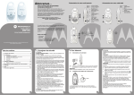
PhlatLight LED
Development Kit Manual
DK-114N Series
Introduction:
Table of Contents
PhlatLight LEDs, from Luminus Devices, have been designed
from the ground up to enable a new class of illumination and
projection systems. Benefiting from a suite of innovations in
chip technology, packaging, and thermal management, PhlatLight LEDs allow designers to achieve efficient light engine designs and deliver high brightness solutions.
Key Features . . . . . . . . . . . . . . . . . . . . . . . . . . . . . . . 2
The DK-114N series of PhlatLight Development Kits was designed for fast and simple evaluation of PhlatLight products.
The included electrical and thermal solutions enable customers to easily breadboard or prototype their system without
time consuming and costly development of driver boards and
heat sinks.
Capable of providing up to 14A and designed to work with all
CBT and PT series parts and their associated applications, the
DK-114N development kits support various different drive conditions and use scenarios.
Available in single or multiple channel versions, the PhlatLight
development kit will reduce development time of a PhlatLight
based solution and provide a platform to build from.
Development Kit Contents . . . . . . . . . . . . . . . . . . . . . . 2
Heat Sink and Driver Module . . . . . . . . . . . . . . . . . . 2
Interface Board . . . . . . . . . . . . . . . . . . . . . . . . . . . 2
Cable Assembly . . . . . . . . . . . . . . . . . . . . . . . . . . . 3
Thermal Interface Materials and Mounting Hardware . . 3
Use Instructions . . . . . . . . . . . . . . . . . . . . . . . . . . . . . 4
Additional Required Lab Equipment . . . . . . . . . . . . . 4
PhlatLight Device Mounting Instructions. . . . . . . . . . . 4
Electrical Setup Instructions . . . . . . . . . . . . . . . . . . 5
Operating Instructions . . . . . . . . . . . . . . . . . . . . . . 7
Appendix A: Electrical Design Considerations . . . . . . . . . 8
Appendix B: Isolated AC-DC Power Supplies . . . . . . . . . . 8
Appendix C: Mechanical Dimensions . . . . . . . . . . . . . . 10
Appendix D: Specifications of Driver Board . . . . . . . . . . 11
Appendix E: Driver Board Schematic . . . . . . . . . . . . . . 11
Appendix F: Cable and Connector Pinout Info . . . . . . . . 12
Appendix G: Future Iterations and Features . . . . . . . . . 12
© 2009 Luminus Devices, Inc. - All Rights Reserved
960017 Rev A
PhlatLight® DK-114N Series Development Kit Manual
Key Features
Heat Sink / Driver Board Assembly
• Drive any CBT or PT series PhlatLight LED up to 14A
The heat sink and driver board are packaged together and
mounted on a common metal substrate (Figure 2). The module
can be left as a free-standing assembly on a bench-top or it can
be mounted on an optical table by using the standard optical
post mounted on the heat sink.
• Pulse frequencies of greater than 40kHz possible
• Analog current control via on-board potentiometers or external voltage
• Simple current and voltage measurements
• Fast rise and fall times - less than 1 microsecond
• Fast current level switching - less than 5 microseconds
Development Kit Contents
The contents of each PhlatLight DK-114A Development Kit will
depend on the number of channels ordered. As shown in Figure
1, each kit includes the following components:
• Interface board
• Heat sink/driver board assembly
• Cable assemblies
• Thermal interface materials and mounting hardware
• User Manual
Each interface board supports up to 3 channels. For configurations of greater than 3 channels, additional interface boards
are included. Additional channels will increase the quantities
of each of these components. The following sections describe
the components in detail.
This development kit was designed with flexible features to allow for easy evaluation of PhlatLight LEDs. It was not optimized for size or for direct integration in end products.
However, the underlying circuit and thermal design can be
used as a reference by system designers. To this effect, the
complete design files including schematics, mechanical drawings, and bills of materials are available upon request.
Figure 2: Heat sink / Driver board Assembly
Heat Sink
The heat sink is a high performance, low cost and compact air
cooled aluminum extrusion. Measuring only 40 mm x 40 mm x
40mm, the heat sink occupies a very small volume. The typical
thermal resistance from heat sink to ambient with the fan in
operation is 0.6 ºC/W, thereby enabling significant power dissipation.
The bolt pattern on the front face of the sink allows for easy
mounting of all CBT and PT series modules. All modules can be
mounted either horizontally or vertically, allowing for easy
prototypes of systems.
Driver Board
The driver board, designed around National Semiconductor’s
LM3433 IC, is designed to provide up to 14A of current to any
PT or CBT series PhlatLight LED. The board is mounted close to
the heat sink and LED to ensure cable lengths are kept at a
minimum (<3”). Longer cable lengths will cause increased current ringing when pulsing the LEDs.
Using a negative-rail, grounded common anode topology, the
LM3433 driver board enables the anodes of multiple PhlatLight
LEDs to be in electrical contact with each other. There is no
need to electrically isolate the anodes of the LEDs from each
other or the heat sink.
Figure 1: Single Channel Evaluation Kit Contents
© 2009 Luminus Devices, Inc. - All Rights Reserved
Page 2
PhlatLight® DK-114N Series Development Kit Manual
The driver board is fully capable of driving the LEDs in either
CW or pulsed mode. PWM frequencies in excess of 40kHz are
feasible. An external function generator is required for generating the pulse trains.
Interface Board
The included interface board is meant to serve as a clean interface from the user supplied lab equipment to the driver
boards. Each interface board is capable of routing power and
signal control to up to three driver boards. A potentiometer
(POT) is included for all three channels to allow for manual adjustment of intensity. Alternatively, the current level can be
controlled via a user supplied voltage signal, which allows for
analog dimming. Likewise, there are inputs for a user supplied
pulse train, which allows for pulsed width modulation (PWM)
of the LEDs.
Figure 4: Included Cable Assemblies
For optimum performance, it is not recommended to increase
the length of the driver to LED cable. A longer cable will result
in decreased performance when pulsing the LEDs.
Thermal Interface Materials (TIMs) and Mounting
Hardware
Also included in the kit are precut sheets of a high performance
thermal interface material (eGraf HiTherm 1205) and the required mounting hardware for the devices.
Figure 3: Interface Board
Cable Assembly
Each development kit includes all of the cables necessary for
proper setup. The primary cables included are as follows:
• Power supply to interface board
• Interface board to driver board - power
• Interface board to driver board - signal
• Interface board to fan
• Driver board to LED
The interface board to driver board cables (power and signal)
and the interface board to fan cable come bundled together.
For pinout information, please refer to Appendix F.
In the cases of using any of the C11 package types (PT85,
PT120, CBT-85, CBT-90 and CBT-120), the driver board to LED
cable is integrated into the driver board.
Figure 5: Left picture: TIM cut for C21 package types. Right
picture: TIM cut for C11 package types.
Mounting screws for the various package types are included.
M2x5 screws are provided for attachment of C21 package types
(PT54, PT39, CBT-54 and CBT-40). M2.5x6 screws are provided
for attachment of C11 package types (PT85, PT120, CBT-85,
CBT-90 and CBT-120).
© 2009 Luminus Devices, Inc. - All Rights Reserved
Page 3
PhlatLight® DK-114N Series Development Kit Manual
User Instructions
The following procedure explains how to setup the PhlatLight
Evaluation Kit. It is recommended that the table be equipped
with ESD protection.
Important Note: The driver board is capable of providing 14A
of current to any device. Not all PhlatLight products can be
powered at 14A. Care must be taken to ensure the proper current is applied to the device. Consult the product data sheets
for current limitations of specific devices.
Figure 6: PhlatLight device and an appropriate thermal interface material
Equipment Required by User
In order to power and use the development kit, some additional equipment is required. Table 1 lists the type of equipment
as well as a suggested part. An additional list of other compatible power supplies is provided in Appendix B.
Important Note: It is very important that the power supply
feature an isolated output. If the AC input ground is tied to
the DC output ground of the power supply, it will cause damage to the driver board. All of the recommended supplies feature an isolated output. Please refer to Appendix A for more
information on these requirements.
Lab Equipment
2. Prepare the heat sink surface by dusting or removing any
particulates that have accumulated on the surface. Place
the thermal pad on the heat sink with pre-drilled holes
matching the hole pattern on the core board of the device
(Figures 7 and 8).
Recommended Part
12V Lab Power Supply
Lambda ZUP20-20
Oscilloscope
Tektronix TDS 3024B
Waveform Generator
Agilent 33220A
Multimeter
Fluke 187
Photodetector
Thorlabs PDA10A
Figure 7: Prepared heat sink with pre-drilled bolt pattern
Table 1: Additional Lab Equipment
PhlatLight Device Mounting Instructions
The following procedure explains the process to properly
mount a PhlatLight device to the included heat sink using the
included thermal interface material and mounting hardware.
The primary goal is to ensure there is good thermal contact between the backside of the copper core-board and the front
face of the heat sink.
1. Use a thermal pad of an area slightly larger than the area
of the core-board (Figure 6).
Figure 8: C21 package type thermal interface material
placed on heat sink
3. Place the device on the thermal pad, taking care that the
hole patterns match (Figure 9).
© 2009 Luminus Devices, Inc. - All Rights Reserved
Page 4
PhlatLight® DK-114N Series Development Kit Manual
age types, a cable is soldered to the board.
The 12” cable assembly, which includes the interface board
to driver board cables as well as the interface board to fan
cable connects as shown in Figures 13 and 14. The 12” cable assembly, as shown in figure 13, connects the control
board to a power supply. This connection is shown in figure
15.
Figure 9: PhlatLight device placed on top of thermal interface material
Important Note: In almost all cases, the connectors will only
insert in one direction. Care must be taken not to force any of
the connections as this may damage the connectors. In the
case that the connector can be connected improperly, the connector and mating cable are clearly marked with either color
coding or lettering. If powered with improper connections,
damage can be caused to the LEDs and circuit boards.
4. Insert screws in the holes of the coreboard and tighten. To
ensure equal pressure is exerted by all screws, alternate
tightening each screw until the board is securely fastened
(Figure 10). The device is now mounted and ready for electrical connections.
Figure 11: CBT-54 LED to driver board cable interface
Figure 10: Fully mounted PhlatLight device
Electrical Connections
The following sections assume that the user has all of the
equipment listed in Table 1.
1. Prepare the power supply and ensure the power supply being used is capable of providing enough power to the devices. A single channel at full power will draw up to ~80W at
12V and 6.5A. If using a variable power supply like the
Lambda ZUP2020, preset the voltage to 12V and set the
current to the maximum. Power off the supply until all connections are established and the board settings are ready.
2. Attach all of the wiring included in the kit. The short, 3”
Figure 12: CBT-54 LED to driver board cable interface
cable connects the LED (C21 package types only) to the
driver board as shown in Figures 11 and 12. For C11 pack© 2009 Luminus Devices, Inc. - All Rights Reserved
Page 5
PhlatLight® DK-114N Series Development Kit Manual
ables the channel and the other controls functionality of
the board.
The enable/disable jumper is located at the positions labeled “ENA1”, “ENA2” and “ENA3”. When these positions
are open (not shorted), the channel is enabled. When they
are closed (shorted), the channel is disabled.
Position the enable/disable jumpers so that the two pins
are closed (shorted).
4. For the other jumper, there are three different possible po-
Figure 13: Driver board to interface board cable connections
sitions for the jumper, each of which enables different
functionality with respect to the control of the driver
board. It is possible to enable the current controlling POT
on the driver board or the POT on the interface board or to
control the current via a 0-5V external input. Table 2 details the various different configurations.
Jumper Location
Function
No jumper
External 0-5 V current control
J20 or J19 or J14
Driver POT current control
J18 or J13 or J15
Control board POT current control
Table 2: Control Board Jumper Locations
Position the jumpers as necessary to enable the type of
control required.
Figure 14: Interface board to driver board cable connections
The locations of these jumpers are shown in Figure 16. The
central channel is detailed in the figure. The locations are
identical in the other two channels.
Figure 15: Interface board to power supply cable interface
3. On each channel of the interface board, there are two
jumpers mounted. One of these jumpers enables or dis-
Figure 16: Jumper Locations
© 2009 Luminus Devices, Inc. - All Rights Reserved
Page 6
PhlatLight® DK-114N Series Development Kit Manual
5. Rotate all of the current controlling POTs (located at “P1”,
“P2” and “P3” on the control board and at “P1” on the driver board) counter-clockwise until they stop. The imbedded
arrow should point towards the “10” on the POT. The POT
is now set at the minimum current setting.
tor in Ohms. The sense resistor value is 0.005Ω. The
output value will the be current going to the LED in amps
(A).
6. The evaluation kit is now ready to be powered on. Turn on
the power supply. The supply will draw a small amount of
power.
7. To turn on any channel, open the enable pin by removing
the jumper. Both the fan on the heat sink and the LED will
power on.
Operating Instructions
There are multiple different ways the PhlatLight DK-114N Development Kit can be operated. The LEDs can be driven in continuous, current controlled mode via on board POTs or through
an external analog voltage. Additionally, each channel has inputs for an external function generator signal to pulse the LEDs
and is capable of pulsing at frequencies of greater than 40kHz.
Sense Resistor Test Studs
Figure 17: Sense resistor location on driver board
1. To change the current when either the interface board or
driver board is enabled, rotate the on board POT. Each
POT will only function when enabled on the interface
board. Clockwise rotation increases the current, while
counter-clockwise rotation will decrease the current.
attach a 0-5V signal to the ADJ test points. These are labeled “T3”, “T4”, “T7”, “T8”, “T11” and “T12”. Each test
point is also labeled with either “GND” or “ADJ”. When
hooking up the 0-5V signal, ensure that the ground cable is
attached to the “GND” test point and the positive cable is
attached to the “ADJ” test point.
The current to the LED will adjust with the voltage signal.
A higher voltage corresponds with a higher current.
It is recommended not to exceed a 5V signal, as components may overheat.
3. To measure the current going to the LED, use a volt meter
and measure the voltage across the sense resistor on the
driver board. For ease of probing, two test studs have been
placed to the left and right of “R15”. Figure 17 shows the
location of the test studs on the driver board. Figure 18
shows a conversion plot between the sense resistor voltage
and the current going to the LED. The current can also be
calculated by the following formula:
V Sense
I LED = --------------R Sense
Equation 1
where VSense is the voltage measured across the sense resistor in Volts (V) and RSense is the value of the sense resis-
16
14
LED Current (A)
2. To change the current when the external adjust is enabled,
18
12
10
8
6
4
2
0
10
30
50
70
90
VSense (mV)
Figure 18: LED Current vs. Vsense voltage
4. To modulate the LEDs through PWM, connect a function
generator to the test points labeled “PWM” and “GND”.
These test points are also labeled “T1”, “T2”, “T5”, “T6”,
“T9” and “T10”. The pulse output should be set to 0-5V,
where 5V represents off and 0V represents on.
Proper operation is best monitored by using a photo detector to observe the light output from the LED.
Figures 16 - 18 show plots of typical waveforms. The device
under test was a blue CBT-54 run at 14A and 50% duty cycle at
30kHz. Actual waveforms will depend on the specific driver
© 2009 Luminus Devices, Inc. - All Rights Reserved
Page 7
PhlatLight® DK-114N Series Development Kit Manual
and LED being used.
It is important to note that all PT and CBT series PhlatLight
LEDs are built in a common anode configuration. That is, the
copper core-board is at a positive electrical potential in operation. If this is not factored into the design, it becomes difficult to connect multiple devices to a common heat sink. The
DK-114N development kit addresses this by configuring the devices in a grounded common anode topology. As a result, the
LED anode is kept at ground and the cathode is at a negative
potential. The LED anode can be in direct electrical contact
with the heat sink without concern of electrical contact with
other LEDs. It is important to note that while the heat sink is
at ground, there is still power passing through it. For further
information, please contact Luminus.
Figure 19: Input and output (optical) pulse
Figure 22: Grounded Common Anode Configuration
Figure 20: Rise time example
This configuration requires that the AC ground line from the
supply providing power to the driver board is isolated from the
DC ground line. A short list of isolated power supplies is provided in Appendix B.
Appendix B: Isolated AC-DC Power Supplies
Table 3 shows a list of isolated AC-DC power supplies. A power
supply with isolated outputs is required to properly drive the
DK-114N drivers. Failure to use a similar power supply will result in a malfunctioning board.
Various different power supplies are listed in the table. For
best efficiency, it is recommended to select a power supply
that closely matches the required power.
Figure 21: Fall time example
Appendix A: Electrical Design Considerations
© 2009 Luminus Devices, Inc. - All Rights Reserved
Page 8
PhlatLight® DK-114N Series Development Kit Manual
Power
Manufacturer
Input
Output V/I
Size
Mounting
Part #
30W
CUI Inc.
AC 85-264 VAC
(47-400Hz)
12V / 2.5A
3.7” x 2” x 0.85”
Thru-hole/SMT
FSK-S30-12U
50W
Omron
AC 85-264VAC
(47-63Hz)
12V / 4.2A
5” x 3.34” x 1.57”
DIN Rail
S8SP-05005
50W
Lambda Power
AC 90-264VAC
(47-63Hz)
12V / 3A
3.62" x 1.46" x 6.26"
Enclosed/Chassis
mount
SWS Series
60W
Globtek Inc.
AC 90-264VAC
(47-440Hz
12V / 5A
5.24” x 2.39” x
1.62”
External/Desktop
DPS50
75W
Lambda Power
C 90-264VAC
(47-63Hz)
12V / 6.3A
3.7" x 1.69" x 6.69"
Enclosed/Chassis
mount
SWS Series
100W
Lambda Power
AC 90-264VAC
(47-63Hz)
12V / 8.5A
3.78" x 1.77" x 7.4”
Enclosed/Chassis
mount
SWS Series
100W
Elpac Power
AC 100-264VAC
(47-63Hz)
12V / 8.3
7.36” x 4.33” x
2.32”
External/Desktop
FWP10012D8F-NC
125W
Power-One Solutions
AC 90-264VAC
(47-63Hz)
12V / 10.5A
5” x 3” x 1.25”
Open Frame
MBP125-1012
120W
AULT Inc.
AC 100-264VAC
(47-63Hz)
12V / 10A
9” x 2.9” x 2”
Medical/External
MW122RA12X
XF01
150W
Lambda Power
AC 90-264VAC
(47-63Hz)
12V / 12.5A
3.9" x 2" X 7.8"
Enclosed/Chassis
mount
SWS Series
Table 3: List of AC/DC power supplies with an isolated output
© 2009 Luminus Devices, Inc. - All Rights Reserved
Page 9
PhlatLight® DK-114N Series Development Kit Manual
Appendix C: Mechanical Dimensions
© 2009 Luminus Devices, Inc. - All Rights Reserved
Page 10
PhlatLight® DK-114N Series Development Kit Manual
Appendix D: Specifications of Driver
Input Specifications
Value
Unit
Note
Input Voltage
12
V
Max Supply current/channel
7
A
Efficiency
>90
%
Output Specifications
Value
Unit
Max output current
17
A
Output current ripple (pulsed)
<10
%
Output Pulse Rise time
<1
us
Output Pulse Fall Time
<1
us
Output Setting Time
<5
us
min current to max
Control Specifications
Value
Unit
Note
Max Pulse Frequency
>40
kHz
Duty Cycle Range
0-100
%
Note
Of set current
Table 4: Driver board Specifications
Appendix E: Driver Board Schematic and Pinout
© 2009 Luminus Devices, Inc. - All Rights Reserved
Page 11
PhlatLight® DK-114N Series Development Kit Manual
Appendix F: Cable and Connector Pinout Info
LED Pin
Driver Board Pin
Comment
Interface Board Pin
Driver Board pin
Comment
Pin 1
Pin 1
Thermistor
Pin 1
Pin 1
GND
Pin 2
Pin 2
Thermistor
Pin 2
Pin 2
Analog ADJ
Pin 3
Pin 4
Pin 6
LED Cathode
Pin 3
Pin 3
POT
Pin 4
Pin 4
Enable
Pin 8
Pin 10
LED Cathode
Pin 4
Pin 5
Pin 5
PWM
Pin 5
LED Cathode
Pin 6
Pin 6
Vinx
Pin 12
Pin 14
Pin 7
Pin 7
Thermistor
Pin 6
Pin 3
Pin 5
LED Anode
Pin 8
Pin 8
Thermistor
Pin 7
Pin 7
Pin 9
LED Anode
Pin 8
Pin 11
Pin 13
LED Anode
Table 5: Interface Board to Driver Board, Signal
Interface Board Pin
Driver Board pin
Comment
Pin 1
Pin 1
-12V
Pin 2
Pin 2
-12V
Pin 3
Pin 3
-12V
Pin 4
Pin 4
GND
Pin 5
Pin 5
GND
Pin 6
Pin 6
GND
Table 6: Interface Board to Driver Board, Power
Table 9: LED to Driver Board, C21 Package Style
LED Pin
Driver Board Pin
Color
Comment
Pin 1
N/A
Green
LED Anode
Pin 2
N/A
Yellow
LED Cathode
Table 10: LED to Driver Board, C11 Package Style
Appendix G: Future Iterations and Features
Interface Board Pin
Fan pin
Comment
Additional features and other enhancements to the development kits are always in process and in development. Among
the planned additional features are:
Pin 1
Pin 1
+12
• Thermistor test points for active monitoring of thermistor
Pin 2
Pin 2
GND
• Built-in pulse train generator for simple PWM testing
Table 7: Interface Board to Fan
Interface Board Pin
Color
Comment
Pin 1
Red
+12
Pin 2
Black
GND
• Built-in fan controller to regulate junction temperature
• Computer based interface for power and color control
For more information about these features, please contact Luminus Devices.
Table 8: Interface Board to Power Supply
© 2009 Luminus Devices, Inc. - All Rights Reserved
Page 12
PhlatLight® DK-114N Series Development Kit Manual
The products, their specifications and other information appearing in this document are subject to change by Luminus Devices without notice. Luminus Devices assumes no liability for errors that may appear in this document, and no liability otherwise arising from the application or use of the
product or information contained herein. None of the information provided herein should be considered to be a representation of the fitness or suitability of the product for any particular application or as any other form of warranty. Luminus Devices’ product warranties are limited to only such
warranties as accompany a purchase contract or purchase order for such products. Nothing herein is to be construed as constituting an additional
warranty. No information contained in this publication may be considered as a waiver by Luminus Devices of any intellectual property rights that
Luminus Devices may have in such information. PhlatLight® is a registered trademark of Luminus Devices, Inc., all rights reserved.
This product is protected by U.S. Patents 6,831,302; 7,074,631; 7,083,993; 7,084,434; 7,098,589; 7,105,861; 7,138,666; 7,166,870; 7,166,871;
7,170,100; 7,196,354; 7,211,831; 7,262,550; 7,274,043; 7,301,271; 7,341,880; 7,344,903; 7,345,416; 7,348,603; 7,388,233; 7,391,059; Patents
Pending in the U.S. and other countries.
Luminus Devices
1100 Technology Park Dr.
Billerica, MA 01821
978-528-8000 (T)
978-528-8001 (F)
E-mail: [email protected]
www.luminus.com
© 2009 Luminus Devices, Inc. - All Rights Reserved
Page 13