1
Chapter 1
Software introduction and installation
1 installation
For Operating system:Windows7/vista/2000/2003/xp.
On Windows7/vista,You must setup by Administrator degree, and on
xp,both by general or administrators .About "Administrator",see
windows help-documents.
Attention: do not link the programmer before installing
installing.
Run Setup.exe when the following picture appeared:
Click the second line "Intl. English," in order to show the process of
installation in English.(It has no relationship of the business of the
language of the Topwin, it has it's own language.) You also can chose
1
the first line for Chinese guide.
Press 【OK】 to continue.
Prsee 【NEXT】
Install the Topwin to c:\topwin6.\
Copying , it may be cost you about 30 seconds.
2
Click 【FINISH】, then to resume the computer.
The icon of Topwin will be appeared on your desktop when the installing
succesd:
Windows need to login the device driver when the first link the
programmer. So following thw step:
Link the USB interface on you computer to programmer by USB
cable.Red light on programmer turns onGreen not yet.
Found new hardware and recognize Top Programmer.that could be save.
Otherwise, the following installing will be fail.
3
Chose the third line "no ,not yet."
Press 【NEXT】
Chose the first line"AUTO STALLING"
Press 【NEXT】
4
Finding the device driver,it may be cost about 10~60seconds.
Press 【CANCEL】to reinstall when overtime.
Found, press【FINISH】to ending.
Now you can run the Topwin to read and write chip when the green
light on programmer turns on.
5
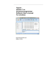
2 Introduction
2.1 The current basic modes that TopWin supported include
TOP 2005,TOP 2007,TOP 2009,TOP 2049,TOP3000,TOP3100.
For Windows7/vista/2000/2003/xp.
The picture following shown the functions on main window of the
topwin6
Functions on main window.
6
Note to new user:
1、 Master the functions and their place on main window.Attention : you
also can find the buffer zone by tag the location on main window
except for click
2、 Programmer has external power supply. different computers has it
own current of USB interface.Programmer could read and write
most of the chip without external power supply except EPROM of
27 series or devices it's current lager then 500 MA.
3、 Display devices correctly while writing.Besides the lock block there
is a schematic,you also can find it in the end of this book on
appendix1.
2.2 Main window
After TopWin start-up,Run offline is more of less the same with run online without read and write chips.Main window of topwin6 will be
showed on the screen as follows:
7
Interface of software:
Menu:
Tool:
8
Buffer:
Operation:
9
Report:
The manual is about the function of main Window.The icons in toolbox
has the same effect with operation in menu, it makes the operation more
convenient.
It will show you the function of the icon when you move the mouse on it.
it is the icon for change English to Chinese.
10
Chapter 2 File Operation
2.1 “File”Menu:
"File" menu includes the file access and print operation, the format
applies to binary system,hexadecimal and JECED. The file menu's
functions are:
2.1.1 open file:
Chose menu“file/open file”,corresponding icon
saved file in buffer zone,operate and pop file window:
Chose the file name you need,appear the dialog.
11
.Shown the
Confirming the file format
1. Chose the file format in "project file",for example a hexadecimal
file, .HEX
2. Chose byte. Many devices should set byte while shown the dialog.
3. Select the way to fill, if it is 00, then the buffer zone so.If it is
FF,so is the blank. Select "save the data"to save the used data.
4. Select the address of buffer zone.start with 0 in normal,we have
more choice for you
5. Press "Yes" to put-in the data to buffer zone,as the follows:
12
Loading file data into the buffer zone
After the loading of file data into the buffer zone,if required to
amend,move the mouse or keyboard to the relative byte and input the
number directly.But the input number must be two hexadecimal
numbers.
If there is a large volume data, and the target data is not in the window,
please use editing key "Page Up",Page Down","Home"and"End"to turn
page.
PLD device introduces JECED formatted file of fuse diagram info with
the extension of ".JFD",after the data is loaded into the buffer zone,it
13
will run as follows:
Chose the correct device then you can open the PLD device.
Data load in to the buffer zone,as follows:
Device PLD loading to buffer
2.1.2 Loading file to buffer :
Such MCU/MPU as PIC12f629,sst89c58,at90s8515,should be written
data and procedure both. Procedure write-in from 0000, data write-in the
address which the device point.(Window under the buffer will
14
show("data from xxxx to xxxx")).The function is help you to write-in
data in the correct address. Loading step is the same with "Open file".
Attention, select the empty device before setup.
Loading of the file data into the buffer zone
Loading of the file data such as MCU/MPU of ATMEGA8L should be
set the byte, example at Chapter 3/3.2.3/Read-Write MCU/MPU/3
2.1.3 Reopen:
Press menu/file/reopen then will be shown.
15
Reopen
Select the file name you want, then loading to buffer.
2.1.4 Save buffer :
The icon
is to save the data in buffer zone.
The data be edited in buffer zone need to save as file, press "file/buffer
save", pop up a dialog as follows:
16
Save buffer
Input a file name as "a", make sure the type as"hexadecimal".
Press"Save"to save the data in file of a.hex.
2.1.5 Open Project:
The extension of project is ".top", product from "Save project".Press
"file/open project",pop up a dialog as follows:
17
Open project
Select project"123.top", press "open".
2.1.6 Save Project:
We loaded data and sets while read-write the device, so we can save the
operation as a project in order to make it easier the next time.
"Project" include buffer ,set device , set up , type . Project is suit of the
process of production, it make sure the device is correct.
Attention:It will be refused if the project being damaged.
The examples about save project is on Chapter 3/3.2.3/read-write
MUC,MPC/example 3 (read-write W79E2051)
2.1.7 Close Project : The function is to close the "Project"
opened .
2.1.8 Print buffer:To print the data in buffer.
Select "file/print buffer",pop up a dialog as follows:
18
Print
Press "Yes" to print the data in buffer zone if the set is correct.
2.2 Modify and editor Menu:
The operation is to edit the data in the buffer zone.
2.2.1 Find:
The operation is to find the named data in the buffer zone. Select the
menu"Modify and editor/find",the standard finding dialog box springs
as follows:
Find
Input ASCL code or two hexadecimal characters(no case sensitive).
Press "Start", also can press"Continue "to find another.
19
2.2.2 Fill Buffer:
The operation can fill in the buffer zone units with required data. Select
"Change Buffer Size", the dialog box springs:
Fill Buffer
Input the start address, end address of the infill block, and the data to be
filled in, and press"Yes".
2.2.3 SUM:
Select "Modify/Sum", pop up a dialog as follows:
Input the start and end address, press "Sum", then you will see the sum.
20
Chapter 3 Device Operation
3.1 Conventional Procedures
Connect to programmer correctly;power indicator (red)turns on.
Run "TopWin.exe",and working indicator(green)turns on.
Select "File" in the main menu,and upload data to the file buffer.
Insert the device into the socket and lock it up,and then be ready for
written-in and read-out operation of device.
Bad device because of the pin rusted, a dialog pop up from the main
Window will show you the bad space:
Dialog show the bad pin
21
3.2 Operate menu:
Operate menu as follows:
Operate menu
A toolbar for improving the speed:
Operate bar on the left head of buffer zone:
22
Integrated operation
Same function but operation between three, menu and toolbox are
operate alone, integrated operation could do more operation and readwrite continually. You can chose what you like.
23
.1 select device by multiple list
3.2.1
3.2.1.1
Chose "operate/select device" ,
then appeared the dialog as follows:
Select device
Select"Type of Device"in the"Type"menu,such as "GAL/PLD".
Select a manufacturer from the list of "Manufacturer",like"ATMEI".
Select a device type from the list of"Device",like select"89c51".
“Fuzzy Find”it means finding with device type or manufacturer, for
example input "51", then you will see MUC/MPC device of series 51.
Narrowed the range and improve the speed.
24
3.2.1.2 Select device by "Tree"
Click
,show dialog as: follows
When you select device without search, you can only use mouse click '+'
to expand tree,you will find out the chip step by step.
25
You can also input part of chip name in edit box,find out the chip
quickly as following:
1.input part of chip name in edit box,like "at89";
2.Click [Search];
3.Click '+' to expand tree,find out chip at length;
4.Select one you want,like "at89c51";
5. Click [OK].
Note:
You can't see the chip name by only click [Search] ,you must
click '+' to expand list step by step.
26
also
3.2.2 Read-write device:
Erasing: Erase all contents if the device memory. After being erased,
the device shows "FF". Only EEP device can use this command, and
EPROM needs to be earsed with ultraviolet radiation.
Blank Check: Before write in device, it is required to check whether
there is a blank. Each byte of the Blank is "FF"(HEX). The check-out
procedures are visually displayed via progress bar. When find out some
non-blank unit, it will exit from the blank check-out procedures and
display the address and data of the non-blank unit.This operation will
check out all address space of EPROM, which is independent of the
device start address or the data length. EPROM can be checked after
being irradiated with uviol lamp,if still fail to pass, it is proved that the
device was already damaged.
Write-in Device: The write-in device is to write the data of the
buffer into a device. The default values of File Start Address are
0,which implies writing data into all the units of this device. While the
length of the data can be up to six bits hexadecimal (HEX) numerals and
the maximal address space is 8M. If necessary, use can follow required
conditions to modify start address, so as to fulfil the intention to write in.
Cautions
Cautions:Before write in device, special attention should be paid to
not to mistake device types,otherwise,device or devices might be
damaged, owing to the device types are totally different, the
corresponding serving programming voltage might be different.
Data Censor: This operation compares the data in the buffer with
those in the device,which is visually displayed via progress bar. When
confront with any unit fails to be censored, it will exit from the data
censor procedures and visually display the fault unit address, the data in
the buffer and the device data. For ensuring the written-in data in the
27
device are correct, the "write-in device" operation should include the
censor procedures. Therefore, no repetition of the same operation is
required.
Write-in Configuration: should be set the configuration of device
before writing because there are so many difference between devices.
Press "device configuration"under the buffer to set it.
Protection: Many EEPROM and FLASH ROM have protection
functions, the device with protection function can only be read out,
instead of being written into, unless invalidata the protection function.
This operation is generally applied with completion of write-in
operation.
Read-out Device : Read out all the data in the device and write
them in the buffer except the device without encryption.
Read-out Manufacturer: The former byte of the two-byte readout code denotes the manufacturer, and the latter one denotes the type.
Such function as read configuration, write-in data, protect, erasing, writein GAL/PLD, Reading shock calibration, userInfo, they will spring
while read-write different MCU/MPU. You could found them in help
file "Config.chm"(in the folder of setup).
3.2.3 Read-Write Device :
Window for read-write are different because of the types of device.
Examples to illustrate how to read-write kinds of devices:mind about
operation
1、 EPROM :
28
Select in Window"select device type"
Type: EPROM
Manufacturer: AMD
Device: AM2764
Press "Confirmation"back to main menu. Loading data to buffer;
insert the same type device in to lock block.
The USB interface offers different current, some larger than 500MA,
others smaller than 300MA, EPROM belongs to large current device, so
advice use the external power supply while writing it.
Operation box left hand beside buffer will spring the three functions of
this device:
Check blank, write code, verify. You could press Press [Go] to write the
buffer data to device, then report shows:
It will the wrong address in report if the device is not blank or can not be
29
write-in: buffer data and device data.
You could press [Run] to write-in much more devices one time. Press it
and a dialog shown as follows:
Take the device away which was written-in.
Insert a new device, lock the block, the it will write-in auto.
You also can find the icon in toolbox:
The three icon front have the function with"Check Blank","Write
Code","Verify".
Press the icon in toolbox to make the operation alone.
Read chip to buffer.
30
Display MFA and type.
It also shows at menu/operation. Erasing by EEPROM if the EPROM
need to rewrite-in.
2、Read-Write EEPROM :
Select in Window"select device type"
Type: EEPROM
Manufacturer: SEEQ
Device: DQ28256
Press "Confirm"back to main menu. Loading data to buffer; insert the
same type device in to lock block.
Operation box left hand beside buffer will spring the four functions of
this device:
Icons spring in toolbox.
31
Differentce between EPROM and EEPROM:1: EEPROM on
programmer while device need to rewrite. So it has more erasing in menu
and toolbox than EPROM. 2:EEPROM could protect the data.
Press [Go], programmer will erase the old data on DQ28256, check the
empty device, write-in data from buffer to device, proofreading.
Press menu "operation/protect" or icon
data written in device, reports as follows:
in toolbox to protect the
。
3、Read-Write MCU/MPU :
MCU/MPU has lots of types such as
AT89c51,PIC12F629,AT90S8535,ATMEG8L,W79E2051.
● Take 89c51 for an example, select the following items from the
Window of"Select Manufacturer/Type"
Type: MCU/MPU
Manufacturer:ATMEL
Device:AT89c51
Press "Confirm",back to the main menu. Input file to buffer zone,insert
the same type device in to lock block.
Operation box left hand beside buffer will spring the five functions of
this device:
32
Read-write MCU/MPU
Select the function which you want,press [Go], programmer will
operate "Erase""Blank""Write code""Verify""Config""Lock". Shows the
reports at the end of the operation:
It will shop the operate and shows the wrong address and data in report if
one of the process has any mistake.
Data can not be read from device to buffer if MCU/MPU had been
locked, press "read chip" or
, you can see FF only.
● Take PIC12F629for an example.select the following items from the
Window of"Select Manufacturer/Type"
Type: MCU/MPU
Manufacturer:MICROCHIP
Device:PIC12F629
33
Press "Confirm", spring the follows picture for pins.
Chip placed
Back to main menu. Loading the data to buffer;insert the same type
device in to lock block.
Operation box left hand beside buffer will spring the six functions of this
device:
34
Have more function such as write data, write configuration.
Normal device has no data section, so needless the function "write data",
but MCU/MPU such as IC12f629,sst89c58,at90s8515 equivalent to a
24xxxx(EEPROM) in it need two file: one is procedure, the other is data,
loading to buffer twice.
Procedure usually start at address 0000, start address of data shows under
the Window of buffer("Data from xxxx to xxxx"), example, device
designated the address is
, user should
loading data on the point address.
If loading by "Open", "Buffer Address" should be input the designated
address. Add "loading data to buffer"in menu in order to make the
process conveniently,so the procedure will set start address automatically
and make sure the start address is correct.
Note,data buffer address is not the real address of device, it just a address
to save the data, the finally address write-in device is decide by
procedure.
Press menu"file/loading data to buffer" then pop up a dialog as follows:
35
Loading data to buffer
Select data file 123.bin. Press "Open"then select the type of file,
Confirmed, shown as follows:
Data loading to designated address in buffer
Press "Config":
Config
Can set the device config such as WDTEN,CP,CPD.Select as you
36
want.Confirm your selection and press [Go], programmer will run the
function one by one.
● Take AT90S853 for an example, select the following items from the
Window of"Select Manufacturer/Type"
Type: MCU/MPU
Manufacturer:ATMEL
Device:AT90S853
Press "Confirm",spring the follows picture for pins.
Operation box left hand beside buffer will spring the five functions of
this device:
AT90S8535 placed
Back to main menu. Loading the data to buffer;insert the same type
device in to lock block.
37
Operation box left hand beside buffer will spring the seven functions of
this device:
Erase, Check blank, Write code, Verify, Lock were introduced in
Chapter 3: Read-write EPROM. Write data was introduced by example
of PIC12F629.
Function of write configuration fuse: press Config besides buffer, shown
as follows :
38
Set config:
set config, effective with RCEN.
Press [Go]to make the device be written.
● Take ATMEG8L for an example, select the following items from the
Window of"Select Manufacturer/Type"
Type: MCU/MPU
Manufacturer:ATMEL
Device:ATMEG8L
Back to main menu. Loading the data to buffer, input file"123.hex"to
buffer.
39
Load data file to buffer:press menu/load data to buffer, shown a dialog
as follows:
Load data to buffer
40
Select file as.bin, press "Open", shown:
Data buffer
Lots of device needless to select byte except this. So take care when
load data: select byte as the following picture:
Select byte
Should chose 16th byte of 2(8th).
41
Press "device config" to set fuse file of device as the following picture
shown:
Fuse configuration settings
Select as you want,then insert the same type of device into the lock
block.Operation box will spring eight functions:
42
Select the function what you want,press [Go]to write-in devices,or press
[Run]to write-in much more devices one time.
43
You can save the config as a project in order to make the next operation
conveniently: press menu/file/save project, pop-up a dialog as follows:
Save project
File named as "mag8.top" ,press "Save".
● Take W79E2051 for an example, select the following items from the
Window of"Select Manufacturer/Type"
Type: MCU/MPU
Manufacturer: WINBOND
Device: 9E2051
Back to main menu. Loading the data to buffer, input file"123.hex"to
buffer.
44
Loading the data to buffer;insert the same type device in to lock block.
Press "device configuration". Select intemal RC for
voltage detection for 2.7V, select "Effective" others.
Set the device config as you want
Operation box will spring fivefunctions:
45
vibration mode ,
Select the function you need in operation box.
Press menu/file/save project, pop-up a dialog as follows:
Save the file named "79e2051.top".
4. Read-write Serial Port Memory
Take 24c02 for example, select the following items from the Window
46
of"Select Manufacturer/Type"
Type: Serial Port Memory
Manufacturer:MICROSHIP
Device: 24LC16
Press "Confirm" back to the main menu, input the data to buffer.
Select the speed to write-in: press "Device Config", shown in buffer: 1
Page delay, 2 Way to write, 3 Way to read, 4 Voltage. Set as you want.
Select Writ-In Speed and Programming Voltage: The
write-in speed of the serial port memory has much variation. It is not
wrong to select the lowest one, while the write-in period might be longer.
If proper speed is required, it is recommended to select different speed
experiments to achieve. When the speed is too high, the adjacent data
might encounter with repeated faults. In generally, it is relatively
suitable to adopt 2-20mS.
Read-out Device : Select menu/operation/read-out device or click
tools
,programmer will read the data to buffer zone.
Write-in Device: Select menu/operation/read-out device or click
tools
.These series of device are written in replacement mode,
namely, these apparatuses are in no need of being erased.
Comparable Data:It has the function as same as those of the "EE
read-write memory".
You could write and verify in one time by using operation box.
47
Press [Go], the report will spring "Complete, the work expand 7.4
seconds." while written-in. It will show you the wrong address and code
if one of the process is wrong.
5. Read-write PLD
Take ATF20V8B/L for example, select the following items from the
Window of"Select Manufacturer/Type".
Type: Programmable Logical Drive
Manufacturer: ATMEL
Device: ATF20V8B/L
Press "confirm" , back to the main Window , input fuse file of
D20V8B(Detailed in 2.1.1 Open File) as follows:
select the function you need in operation box , check it . Check all if all
of them you need.
48
Press [Go],to erase, check blank, write code, verify, lock. Separate
operation:
Check blank and Verify data: has the same function with "Read-Write
EEPROM".
Erase device:
Erase the originalcontent in device, concluding and array fuse,
configuration control field, field signs.
Lock:
The same function with ""Read-Write EEPROM"
3.3.3 SRAM Test
With the example of 628128,select in Select Manufacturer/Type box
Category:SRAM Test
Manufacturer:STAND
Part Series:628128 128K*8
Press "Yes" button,pop up SRAM Test Window as follows:
The menu is chiefly used to test the common static storage SRAM. Press
"Start"[Go],and the programmer test each byte of memory to ensure the
49
test is performed stably.
Reading and writing operation of self-battery static memory are reserved
in the operational functions.
Finished the operation,report
Otherwise,
50
Chapter 4 Display
4.1 Show Project Buffer:
To show the project which was load to buffer .
4.2 Show Data Buffer:
To show the data which was load to buffer. It just work on the device
which selected to be write-in.
4.3 Show config:
Will show the config of device by selected.
4.4 Information of device:
51
Chapter 5 Tools
5.1 Settings:
topwin6 offer the function of write-in "Additional Information", it
means short message besides the user code file, it can change every time
while write-in, you can use it to lock data or others you want. The
Window as follows:
It has three tab in this Window for you to select what you need.
1. "Linear incremental" tab:
(1). Type the address of additional information in editor box of "start
address", the address should be the rest space in device, generally behind
the file. If the space of device were filled by user code file, the additional
information can not be write-in.
(2). Select bytes in length in editor box of "bytes in length". Most eight
bytes(2 M 64-bit integer).
(3). Type the initial round in "Numerical" editor box, the initial round
will change later.
52
(4). Select increase in "incremental" editor box, it is also the initial
round, or is reduction if add a negative in front of it.
(5).Select "Allow linear incremental".
2. "Date And Time" tab:
(1). Type date and time in "start address" editor box.
(2). Select "Allow Date And Time".
(3). Date and time is from computer, needless input yourself.
53
3. Others:
(1). Check state of pin contact: the programmer will check the state of
pin contact ever time, report at once if one of pin was broken. And stop
the process.
(2). Check current over the limited: check current over the limited
always effective even if the select had been prohibited.
54
5.2 Information of programmer:
5.3 Programmer self-test:
Select the function, programmer will test itself and shown in report:
At the end it shown:
Show the error number:
55
5.4 IC Test::
Test good or bad and logic functions of thousands types of devices
series of 74,45,40.
Type: test TTL/CMOS
Press "Confirm", pop-up a test Window as follows:
Test TTL/CMOS
Select the type of series of device need to be tested. A horn ring if the
device is good, otherwise ring bell three times.
The function is additional function, so it is normal a very small can not
be tested or quit.
56
57
58