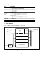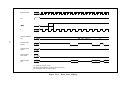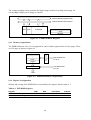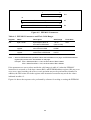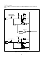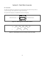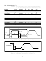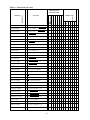
1
OMC301495272
Hitachi Single-Chip Microcomputer
H8/3102
HD6483102
User’s Manual
Preface
The H8/3102 is a single-chip microcomputer built around a high-speed H8/300 CPU core. On-chip
facilities include 8-kbyte EEPROM, 16-kbyte ROM, 512-byte RAM, and two I/O ports.
On-chip EEPROM makes the H8/3102 ideal for applications requiring nonvolatile data storage,
including smart cards and portable data banks. Security functions protect data in the on-chip ROM
and EEPROM against external reading and writing.
This manual describes the H8/3102 hardware. For details of the instruction set, refer to the H8/300
Series Programming Manual.
Contents
Section 1.
1.1
1.2
1.3
Overview .............................................................................................................................
Block Diagram.....................................................................................................................
Pin Arrangement and Functions ..........................................................................................
1.3.1
Pin Arrangement ...................................................................................................
1.3.2
Pin Functions.........................................................................................................
Section 2.
2.1
2.2
2.3
2.4
2.5
2.6
2.7
Overview ............................................................................................................ 1
1
2
3
3
5
CPU...................................................................................................................... 6
Overview .............................................................................................................................
2.1.1
Features .................................................................................................................
2.1.2
CPU Registers .......................................................................................................
Register Descriptions...........................................................................................................
2.2.1
General Registers ..................................................................................................
2.2.2
Control Registers...................................................................................................
2.2.3
Initial Register Values ...........................................................................................
Data Formats........................................................................................................................
2.3.1
Data Formats in General Registers .......................................................................
2.3.2
Memory Data Formats ..........................................................................................
Addressing Modes ...............................................................................................................
2.4.1
Addressing Modes.................................................................................................
2.4.2
Effective Address Calculation...............................................................................
Instruction Set......................................................................................................................
2.5.1
Data Transfer Instructions.....................................................................................
2.5.2
Arithmetic Operations...........................................................................................
2.5.3
Logic Operations...................................................................................................
2.5.4
Shift Operations ....................................................................................................
2.5.5
Bit Manipulations..................................................................................................
2.5.6
Branching Instructions ..........................................................................................
2.5.7
System Control Instructions..................................................................................
2.5.8
EEPROM Write Instruction ..................................................................................
Operating States...................................................................................................................
2.6.1
Overview...............................................................................................................
2.6.2
Program Execution State.......................................................................................
2.6.3
Exception Processing State ...................................................................................
2.6.4
Power-Down State ................................................................................................
Exception Processing...........................................................................................................
6
6
7
8
8
8
9
10
11
12
13
13
15
18
20
22
23
23
25
29
31
32
33
33
34
34
34
35
2.8
2.9
2.7.1
Overview...............................................................................................................
2.7.2
Reset .....................................................................................................................
2.7.3
Interrupts ...............................................................................................................
Power-Down State ...............................................................................................................
2.8.1
Overview...............................................................................................................
2.8.2
Transition to Sleep Mode ......................................................................................
2.8.3
Exit from Sleep Mode ...........................................................................................
Basic Timing........................................................................................................................
2.9.1
On-Chip Memory (RAM, ROM, EEPROM)........................................................
2.9.2
Register Field (I/O, EEPROM).............................................................................
2.9.3
Non-Existent Addresses........................................................................................
35
35
37
38
38
38
38
40
40
40
41
Section 3.
Memory Map ..................................................................................................... 42
Section 4.
RAM .................................................................................................................... 43
4.1
Overview ............................................................................................................................. 43
4.1.1
Block Diagram ...................................................................................................... 43
Section 5.
5.1
Overview ............................................................................................................................. 44
5.1.1
Block Diagram ...................................................................................................... 44
5.1.2
Security ................................................................................................................. 44
Section 6.
6.1
6.2
6.3
6.4
ROM .................................................................................................................... 44
EEPROM ............................................................................................................ 45
Overview .............................................................................................................................
6.1.1
Features .................................................................................................................
6.1.2
Block Diagram ......................................................................................................
6.1.3
Memory Organization ...........................................................................................
6.1.4
Register Configuration..........................................................................................
Register Descriptions...........................................................................................................
6.2.1
EEPROM Control Register (ECR) .......................................................................
6.2.2
EEPROM Protection Register (EPR)....................................................................
EEPROM Read Operation...................................................................................................
EEPROM Write and Erase Operations................................................................................
6.4.1
Write/Erase Sequence ...........................................................................................
6.4.2
Rewrite ..................................................................................................................
6.4.3
Erase......................................................................................................................
6.4.4
Overwrite ..............................................................................................................
45
45
45
46
46
47
47
48
48
49
49
51
51
52
6.5
6.6
Write/Erase Protection.........................................................................................................
6.5.1
Protect Bits............................................................................................................
6.5.2
Protection Procedure .............................................................................................
6.5.3
Reading the Protect Bits........................................................................................
Notes ...............................................................................................................................
Section 7.
7.1
7.2
7.3
7.4
8.1
56
57
58
58
58
59
60
61
Clock Pulse Generator .................................................................................... 62
Overview ............................................................................................................................. 62
Section 9.
9.1
9.2
I/O Port ............................................................................................................... 56
Overview .............................................................................................................................
7.1.1
Block Diagram ......................................................................................................
7.1.2
Register Configuration..........................................................................................
Register Descriptions...........................................................................................................
7.2.1
Data Register (DR)................................................................................................
7.2.2
Data Direction Register (DDR).............................................................................
Pin Functions .......................................................................................................................
I/O Pin Timing .....................................................................................................................
Section 8.
52
52
53
54
54
Electrical Characteristics ................................................................................ 63
Absolute Maximum Ratings ................................................................................................
Electrical Characteristics .....................................................................................................
9.2.1
DC Characteristics (5 V).......................................................................................
9.2.2
AC Characteristics (5 V).......................................................................................
9.2.3
DC Characteristics (3 V).......................................................................................
9.2.4
AC Characteristics (3 V).......................................................................................
63
63
63
64
66
67
Appendices
Appendix A. Instruction Set ................................................................................................... 69
Appendix B. Operation Code Map ....................................................................................... 76
Appendix C. Register Field .................................................................................................... 78
C.1
C.2
Register Field (1) ................................................................................................................. 78
Register Field (2) ................................................................................................................. 79
Appendix D. I/O Port Block Diagram .................................................................................. 81
Appendix E. External Dimensions ....................................................................................... 82
Section 1. Overview
1.1 Overview
The H8/3102 is a single-chip microcomputer built around a high-speed H8/300 CPU core. An
8-kbyte EEPROM, 16-kbyte ROM, 512-byte RAM, and 2-bit I/O port are integrated onto the
H8/3102 chip.
Operating at a maximum 5-MHz clock rate at 5 V, the H8/300 CPU rapidly executes bitmanipulation instructions, arithmetic and logic instructions, and data transfer instructions.
Security functions protect the data in the ROM and EEPROM.
Table 1-1 lists the features of the H8/3102.
Table 1-1. Features
Item
Specification
CPU
H8/300 CPU
Two-way general register configuration
• Sixteen 8-bit registers, or
• Eight 16-bit registers
High-speed operation
• Maximum clock rate: 5 MHz (with 10-MHz external clock input at 5 V)
• Add/subtract:
0.4 µs
• Multiply/divide:
2.8 µs
Streamlined, concise instruction set
• Instruction length: 2 or 4 bytes
• Register-register arithmetic and logic operations
• MOV instruction for data transfer between registers and memory
Instruction set features
• Multiply instruction (8 bits × 8 bits)
• Divide instruction (16 bits ÷ 8 bits)
• Bit-accumulator instructions
• Register-indirect specification of bit positions
On-chip
memory
EEPROM
• 8 kbytes
• Written by EEPMOV instruction
• Page (32 bytes) write and erase
• Protected against accidental writing and erasing
• On-chip voltage pumping circuit
ROM
• 16 kbytes
RAM
• 512 bytes
I/O ports
Two general-purpose input/output ports (I/O–1/IRQ also used for interrupts)
1
Table 1-1. Features (cont)
Item
Specification
Interrupts
One external interrupt lines: I/O–1/IRQ
• Used for interrupt input in sleep mode
Power
Single-voltage power supply
• 4.5 V to 5.5 V, or
• 2.7 V to 3.3 V
Clock
frequency
range
External clock input
• fCLK = 1 MHz to 10 MHz (VCC = 4.5 V to 5.5 V)
• fCLK = 1 MHz to 5 MHz (VCC = 2.7 V to 3.3 V)
Internal clock input
• fOP = 500 kHz to 5 MHz (VCC = 4.5 V to 5.5 V)
• fOP = 500 kHz to 2.5 MHz (VCC = 2.7 V to 3.3 V)
Power-down
state
•
Sleep mode
Others
•
Input clock frequency monitor
1.2 Block Diagram
Figure 1-1 shows an internal block diagram of the H8/3102.
I/O–1/IRQ
I/O–2
V CC
H8/300
CPU
V SS
I/O port
Address bus
RES
System control logic
ROM: 16 kbytes
RAM: 512 bytes
CLK
Clock
divider
EEPROM: 8 kbytes
Figure 1-1. Block Diagram
2
Data bus
1.3 Pin Arrangement and Functions
1.3.1 Pin Arrangement
CLK
I/O-1
NC
NC
0.3
4.4
0.2
3.3
0.2
0.2
3.3
2.46
0.2
2.34
10.6
NC
2.46
RES
2.34
VSS
0.2
VCC
0.2
0.2
Figure 1-2 shows the standard COB bonding pad pattern of the H8/3102 chip.
0.3
12.0
Unit: mm
Figure 1-2. Standard COB Pattern (Electrode Surface)
3
VCC
VSS
CLK
I/O-1/IRQ
RES
CLK
I/O-2
VCC
VSS
User pad
Figure 1-3. Bonding Pad Arrangement
4
1.3.2 Pin Functions
Table 1-2 lists the functions of the H8/3102 pins.
Table 1-2. Pin Functions
Type
Symbol
I/O
Name and Description
Power supply
VCC*1
I
Power supply: 4.5 V to 5.5 V or 2.7 V to 3.3 V
VSS*1
I
Ground: 0 V
Clock
CLK*1
I
Clock: external clock input
Reset
RES*2
I
Reset: low input resets the chip
Ports
I/O-1/IRQ*3
I/O
I/O port 1:
Interrupt:
I/O-2*3
I/O
I/O port 2:
One-bit data input/output port. Software can
select input or output.
In sleep mode, this port receives interrupt input.
One-bit data input/output port. Software can
select input or output.
Notes: *1 VCC, VSS, and CLK have two bonding pads apiece. When the H8/3102 is mounted as a bare
chip, either or both pads may be used. When only one pad is used, the other unused pad
should be left open without connecting anything. When both CLK pins are used, the same clock
should be input to both pins.
*2 An input pull-down MOS is connected to the RES pin as shown in figure 1-3 to avoid incorrect
operation when RES pin input is at high-impedance. The input pull-down MOS therefore
consumes current when high level is input to the RES pin while the chip is operating. During
sleep mode, the input pull-down MOS is in off-state.
Input buffer
RES
pin
Sleep mode
Internal
RES signal
Input pull-down MOS
VSS
Figure 1-4. Block Diagram of RES Pin
*3 I/O-1/IRQ and I/O-2 pins can be used as an I/O port and I/O-1/IRQ pin can be used as an
interrupt input pin. When these pins are not used, they should be left open without connecting
anything.
Input pull-up MOS’s are connected to these pins.
See section 7, I/O Port, for details on the I/O-1/IRQ and I/O-2 pins.
5
Section 2. CPU
2.1 Overview
The H8/3102 has the generic H8/300 CPU: an 8-bit central processing unit with a speed-oriented
architecture featuring sixteen general registers. This section describes the CPU features and
functions, including a concise description of the addressing modes and instruction set. For further
details on the instructions, see the H8/300 Series Programming Manual.
2.1.1 Features
The main features of the H8/300 CPU are listed below.
•
Two-way register configuration
— Sixteen 8-bit general registers, or
— Eight 16-bit general registers
•
Instruction set with 55 basic instructions*, including:
— Multiply and divide instructions
— Powerful bit-manipulation instructions
— EEPROM write instruction
•
Eight addressing modes
—
—
—
—
—
—
—
—
•
Register direct
Register indirect
Register indirect with displacement
Register indirect with post-increment or pre-decrement
Absolute address
Immediate
Program-counter relative
Memory indirect
Rn
@Rn
@(d:16, Rn)
@Rn+ or @–Rn
@aa:8 or @aa:16
#xx:8 or #xx:16
@(d:8, PC)
@@aa:8
64-kbyte address space
Note: * The H8/300 CPU has 57 basic instructions, but the H8/3102 uses only 55 of them. The
MOVFPE and MOVTPE instructions are not used.
6
•
High-speed operation
— All frequently-used instructions are executed in two to four states
— Maximum clock rate is 5 MHz (with 10-MHz external clock input at 5 V)
— 8- or 16-bit register-register add or subtract:
0.4 µs
— 8 × 8-bit multiply:
2.8 µs
— 16 ÷ 8-bit divide:
2.8 µs
•
Power-down mode
— SLEEP instruction
2.1.2 CPU Registers
Figure 2-1 shows the register structure of the H8/300 CPU. There are two groups of registers: the
general registers and control registers.
General registers (Rn)
7
0
R0H
R1H
R2H
R3H
R4H
R5H
R6H
R7H
7
0
R0L
R1L
R2L
R3L
R4L
R5L
R6L
R7L
(SP)
Control registers (CR)
15
0
PC
CCR
7
6
5
4
I
U H U N Z V C
Notation:
SP:
PC:
CCR:
I:
U:
H:
N:
Z:
V:
C:
Stack Pointer
Program Counter
Condition Code Register
Interrupt mask bit
User bit
Half-carry flag
Negative flag
Zero flag
Overflow flag
Carry flag
Figure 2-1. CPU Registers
7
3
2
1 0
2.2 Register Descriptions
2.2.1 General Registers
All the general registers can be used as both data registers and address registers.
When used as data registers, they can be accessed as 16-bit registers (R0 to R7), or the high bytes
(R0H to R7H) and low bytes (R0L to R7L) can be accessed separately as 8-bit registers.
When used as address registers, the general registers are accessed as 16-bit registers (R0 to R7).
Registers R4L, R5, and R6 have special functions when the EEPMOV (EEPROM write) instruction
is executed.
R7 also functions as the stack pointer, used implicitly by hardware in processing exceptions and
subroutine calls. In assembly-language coding, R7 can also be denoted by the symbol SP. As
indicated in figure 2-2, SP (R7) points to the top of the stack.
Free area
SP (R7)
Stack area
Figure 2-2. Stack Pointer
2.2.2 Control Registers
The CPU control registers include a 16-bit program counter (PC) and an 8-bit condition code
register (CCR).
(1) Program Counter (PC): This 16-bit register indicates the address of the next instruction the
CPU will execute. All instructions are fetched 16 bits (1 word) at a time, so the least significant bit
of the PC is ignored (always regarded as 0).
(2) Condition Code Register (CCR): This 8-bit register contains internal CPU status information,
including the interrupt mask bit (I) and half-carry (H), negative (N), zero (Z), overflow (V), and
carry (C) flags.
Bit 7—Interrupt Mask Bit (I): Masks interrupts when set to 1. This bit is set to 1 at the beginning
of exception processing.
8
Bit 6—User Bit (U): Can be written and read by software for its own purposes (using the LDC,
STC, ANDC, ORC, and XORC instructions).
Bit 5—Half-Carry Flag (H): When the ADD.B, ADDX.B, SUB.B, SUBX.B, CMP.B, or NEG.B
instruction is executed, this flag is set to 1 if there is a carry or borrow at bit 3, and is cleared to 0
otherwise.
The H flag is used implicitly by the DAA and DAS instructions.
When the ADD.W, SUB.W, or CMP.W instruction is executed, the H flag is set to 1 if there is a
carry or borrow at bit 11, and is cleared to 0 otherwise.
Bit 4—User Bit (U): Can be written and read by software for its own purposes (using the LDC,
STC, ANDC, ORC, and XORC instructions).
Bit 3—Negative Flag (N): Indicates the most significant bit (sign bit) of data.
Bit 2—Zero Flag (Z): Set to 1 to indicate zero data, and cleared to 0 to indicate non-zero data.
Bit 1—Overflow Flag (V): Set to 1 when an arithmetic overflow occurs, and cleared to 0 at other
times.
Bit 0—Carry Flag (C): Set to 1 when a carry occurs, and cleared to 0 otherwise. Used by:
•
•
•
Add instructions, to indicate a carry
Subtract instructions, to indicate a borrow
Shift and rotate instructions, to store the value shifted out of the end bit
The carry flag is also used as a bit accumulator by bit manipulation instructions.
Some instructions leave some or all of the flag bits unchanged. The LDC, STC, ANDC, ORC, and
XORC instructions enable the CPU to load and store the CCR, and to set or clear selected bits by
logic operations. The N, Z, V, and C flags are used as branching conditions for conditional
branching (Bcc) instructions.
Refer to the H8/300 Series Programming Manual for the action of each instruction on the flag bits.
2.2.3 Initial Register Values
When the CPU is reset, the program counter (PC) is loaded from the vector table and the I bit in the
CCR is set to 1. The other CCR bits and the general registers are not initialized. In particular, the
stack pointer (R7) is not initialized. To prevent program crashes the stack pointer should be
initialized by software, by the first instruction executed after a reset.
9
2.3 Data Formats
The H8/300 CPU can process 1-bit data, 4-bit (BCD) data, 8-bit (byte) data, and 16-bit (word) data.
•
Bit manipulation instructions operate on 1-bit data specified as bit n (n = 0, 1, 2, ..., 7) in a
byte operand.
•
All arithmetic instructions except ADDS and SUBS can operate on byte data.
•
The MOV.W, ADD.W, SUB.W, CMP.W, ADDS, SUBS, MULXU (8 bits × 8 bits), and DIVXU
(16 bits ÷ 8 bits) instructions operate on word data.
•
The DAA and DAS instructions perform decimal arithmetic adjustments on byte data in packed
BCD form. Each nibble of the byte is treated as a decimal digit.
10
2.3.1 Data Formats in General Registers
Data of all the sizes above can be stored in general registers as shown in figure 2-3.
Data type
Register no.
Data format
7
1-bit data
RnH
0
7
6
5
4
3
2
1
don't care
0
7
1-bit data
Byte data
Byte data
Word data
don't care
RnL
RnH
Rn
0
MSB
LSB
don't care
RnH
6 5
RnL
0
7
0
MSB
LSB
0
MSB
LSB
4 3
Upper digit
0
don't care
Lower digit
don't care
Notation:
RnH:
RnL:
MSB:
LSB:
2 1
don't care
7
4-bit BCD data
4 3
15
7
4-bit BCD data
7
7
RnL
0
General register (high byte)
General register (low byte)
Most significant bit
Least significant bit
Figure 2-3. Register Data Formats
11
4 3
Upper digit
0
Lower digit
2.3.2 Memory Data Formats
Figure 2-4 indicates the data formats in memory. Word data stored in memory must always begin at
an even address. In word access the least significant bit of the address is regarded as 0. If an odd
address is specified, no address error occurs but the access is performed at the preceding even
address. This rule affects the MOV.W instruction, and also applies to instruction fetching.
Data type
Address
Data format
7
1-Bit data
Address n
7
Byte data
Address n
MSB
Even address
Odd address
MSB
Word data
Byte data (CCR) on stack
Even address
Odd address
Word data on stack
Even address
Odd address
0
6 5
4 3
2 1
0
LSB
Upper 8 bits
Lower 8 bits
LSB
MSB
CCR
LSB
MSB
CCR*
LSB
MSB
LSB
Note: * Ignored on return.
Notation:
CCR: Condition code register
Figure 2-4. Memory Data Formats
When the stack is accessed using R7 as an address register, word access should always be
performed. When the CCR is pushed on the stack, two identical copies of the CCR are pushed to
make a complete word. When they are restored, the lower byte is ignored.
12
2.4 Addressing Modes
2.4.1 Addressing Modes
The H8/300 CPU supports the eight addressing modes listed in table 2-1. Each instruction uses a
subset of these addressing modes.
Table 2-1. Addressing Modes
No.
➀
➁
➂
➃
➄
➅
➆
➇
Addressing Mode
Register direct
Register indirect
Register indirect with displacement
Register indirect with post-increment
Register indirect with pre-decrement
Absolute address
Immediate
Program-counter relative
Symbol
Rn
@Rn
@(d:16, Rn)
@Rn+
@–Rn
@aa:8 or @aa:16
#xx:8 or #xx:16
@(d:8, PC)
Memory indirect
@@aa:8
➀ Register Direct—Rn: The register field of the instruction specifies an 8- or 16-bit general
register containing the operand.
Only the MOV.W, ADD.W, SUB.W, CMP.W, ADDS, SUBS, MULXU (8 bits × 8 bits), and
DIVXU (16 bits ÷ 8 bits) instructions have 16-bit operands.
➁ Register Indirect—@Rn: The register field of the instruction specifies a 16-bit general register
containing the address of the operand.
➂ Register Indirect with Displacement—@(d:16, Rn): The instruction has a second word (bytes
3 and 4) containing a displacement which is added to the contents of the specified general register
to obtain the operand address.
This mode is used only in MOV instructions. For the MOV.W instruction, the resulting address
must be even.
➃ Register Indirect with Post-Increment or Pre-Decrement—@Rn+ or @–Rn:
•
Register indirect with post-increment— @Rn+
The @Rn+ mode is used with MOV instructions that load registers from memory.
The register field of the instruction specifies a 16-bit general register containing the address of
the operand. After the operand is accessed, the register is incremented by 1 for MOV.B or 2 for
MOV.W. For MOV.W, the original contents of the 16-bit general register must be even.
13
•
Register indirect with pre-decrement—@–Rn
The @–Rn mode is used with MOV instructions that store register contents to memory.
The register field of the instruction specifies a 16-bit general register which is decremented by 1
or 2 to obtain the address of the operand in memory. The register retains the decremented value.
The size of the decrement is 1 for MOV.B or 2 for MOV.W. For MOV.W, the original contents
of the 16-bit general register must be even.
➄ Absolute Address—@aa:8 or @aa:16: The instruction specifies the absolute address of the
operand in memory.
The absolute address may be 8 bits long (@aa:8) or 16 bits long (@aa:16). The MOV.B and bit
manipulation instructions can use 8-bit absolute addresses. The MOV.B, MOV.W, JMP, and JSR
instructions can use 16-bit absolute addresses.
For an 8-bit absolute address, the upper 8 bits are assumed to be 1 (H'FF). The address range is
H'FF00 to H'FFFF (65280 to 65535).
➅ Immediate— #xx:8 or #xx:16: The instruction contains an 8-bit operand (#xx:8) in its second
byte, or a 16-bit operand (#xx:16) in its third and fourth bytes. Only MOV.W instructions can
contain 16-bit immediate values.
The ADDS and SUBS instructions implicitly contain the value 1 or 2 as immediate data. Some bit
manipulation instructions contain 3-bit immediate data in the second or fourth byte of the
instruction, specifying a bit number.
➆ Program-Counter Relative—@(d:8, PC): This mode is used in the Bcc and BSR instructions.
An 8-bit displacement in byte 2 of the instruction code is sign-extended to 16 bits and added to the
program counter contents to generate a branch destination address. The possible branching range is
–126 to +128 bytes (–63 to +64 words) from the current address. The displacement should be an
even number.
➇ Memory Indirect—@@aa:8: This mode can be used by the JMP and JSR instructions. The
second byte of the instruction code specifies an 8-bit absolute address. The word located at this
address contains the branch destination address.
The upper 8 bits of the absolute address are assumed to be 0 (H'00), so the address range is from
H'0000 to H'00FF (0 to 255). Note that addresses H'0000 to H'0007 (0 to 7) are located in the
vector table.
If an odd address is specified as a branch destination or as the operand address of a MOV.W
instruction, the least significant bit is regarded as 0, causing word access to be performed at the
address preceding the specified address. See section 2.3.2, Memory Data Formats for further
information.
14
2.4.2 Effective Address Calculation
Table 2-2 shows how effective addresses are calculated in each of the addressing modes.
Arithmetic and logic instructions use register direct addressing ➀. The ADD.B, ADDX, SUBX,
CMP.B, AND, OR, and XOR instructions can also use immediate addressing ➅.
Data transfer instructions can use all addressing modes except program-counter relative ➆ and
memory indirect ➇.
Bit manipulation instructions use register direct ➀, register indirect ➁, or absolute ➄ addressing to
specify a byte operand, and 3-bit immediate addressing ➅ to specify a bit position in that byte. The
BSET, BCLR, BNOT, and BTST instructions can also use register direct addressing ➀ to specify
the bit position.
15
Table 2-2. Effective Address Calculation
No.
1
Addressing Mode,
Instruction Format
Effective Address
Calculation
Effective
Address
3
Register direct Rn.
0
regm
15
8 7
op
4 3
3
0
regn
0
regm regn
Operands are contained in
registers m and n
2
Register indirect @Rn
15
76 4 3
0
0
16-bit register contents
15
0
15
0
15
0
15
0
reg
op
3
15
Register indirect
with displacement
15
@(d:16, Rn)
0
16-Bit register contents
15
76 4 3
⊕
0
16-Bit displacement
reg
op
disp
4
Register indirect
with post-increment
@Rn+
15
0
16-Bit register contents
15
op
76 4 3
reg
0
⊕
1 or 2*
Register indirect
with pre-decrement
15
@– Rn
0
16-Bit register contents
15
op
76 4 3
reg
0
1 or 2*
* 1 for a byte operand,
2 for a word operand
16
Table 2-2. Effective Address Calculation (cont)
No.
5
Addressing Mode,
Instruction Format
Effective Address
Calculation
Effective
Address
Absolute address @aa:8
15
8 7
op
15
8 7
0
H'FF
0
abs
Absolute address @aa:16
15
15
0
0
op
abs
6
Immediate #xx:8
15
8 7
op
0
Operand is 1-byte
immediate data
0
Operand is 2-byte
immediate data
#IMM
Immediate
#xx:16
15
op
#IMM
7
15
PC-relative @(d:8, PC)
0
PC contents
15
0
15
0
⊕
15
8 7
op
8
0
Signextensi
disp
disp
Memory indirect @@aa:8
15
8 7
op
0
abs
15
8 7
0
H'00
16-bit memory contents
Notation:
reg, regm, regn:
op:
disp:
IMM:
abs:
General registers
Operation field
Displacement
Immediate data
Absolute address
17
2.5 Instruction Set
The H8/3102 can use a total of 55 instructions, which are grouped by function in table 2-3.
Note: The H8/300 CPU has 57 basic instructions, but the H8/3102 uses only 55 of them. The
MOVFPE and MOVTPE instructions are not used.
Table 2-3. Instruction Set
Function
Data transfer
Arithmetic operations
Logic operations
Shift
Bit manipulation
Branch
System control
EEPROM write
Notes: *1
*2
Instructions
MOV, PUSH*1, POP*1
ADD, SUB, ADDX, SUBX, INC, DEC, ADDS, SUBS,
DAA, DAS, MULXU, DIVXU, CMP, NEG
AND, OR, XOR, NOT
SHAL, SHAR, SHLL, SHLR, ROTL, ROTR, ROTXL, ROTXR
BSET, BCLR, BNOT, BTST, BAND, BIAND, BOR,
BIOR, BXOR, BIXOR, BLD, BILD, BST, BIST
Bcc*2, JMP, BSR, JSR, RTS
SLEEP, LDC, STC, ANDC, ORC, XORC, NOP, RTE
EEPMOV
Types
1
14
4
8
14
5
8
1
Total 55
POP Rn is identical to MOV.W @SP+, Rn. PUSH Rn is identical to MOV.W Rn, @–SP.
Bcc is a conditional branch instruction in which cc represents a condition code.
18
Tables 2-4 to 2-11 give a concise summary of the instructions in each functional group. The
following notation is used in these tables to describe the operations performed.
Operation Notation
Rd
General register (destination)
Rs
General register (source)
Rn
General register
(EAd)
Destination operand
(EAs)
Source operand
CCR
Condition code register
N
N (negative) bit of CCR
Z
Z (zero) bit of CCR
V
V (overflow) bit of CCR
C
C (carry) bit of CCR
PC
Program counter
SP
Stack pointer
#IMM
Immediate data
disp
Displacement
+
Addition
–
Subtraction
×
Multiplication
÷
Division
∧
AND logical
∨
OR logical
⊕
Exclusive OR logical
→
Move
¬
Not
:3, :8, :16
3-, 8-, or 16-bit length
19
2.5.1 Data Transfer Instructions
Table 2-4 describes the data transfer instructions.
Table 2-4. Data Transfer Instructions
Instruction
MOV
Size*
B/W
POP
W
PUSH
W
Function
(EAs) → Rd, Rs → (EAd)
Moves data between two general registers or between a general register
and memory, or moves immediate data to a general register.
The Rn, @Rn, @(d:16, Rn), @aa:16, #xx:16, @–Rn, and @Rn+ addressing
modes are available for byte or word data. The #xx:8, @aa:8 addressing
mode are available for byte data only.
Specify word-size operands for @–R7 and @R7+.
@SP+ → Rn
Pops a 16-bit general register from the stack. Identical to MOV.W @SP+,
Rn.
Rn → @–SP
Pushes a 16-bit general register onto the stack. Identical to MOV.W Rn,
@–SP.
Note: * Size: operand size
B: Byte
W: Word
20
Figure 2-5 shows the object code formats of the data transfer instructions.
15
8
7
op
0
rm
15
8
op
0
rm
15
8
@Rm ← → Rn
rn
7
op
Rm → Rn
rn
7
0
rm
rn
@(d:16, Rm) ← → Rn
disp
15
8
7
op
8
op
0
rm
15
rn
7
rn
8
@aa:8 ← → Rn
7
0
op
rn
@aa:16 ← → Rn
abs
15
8
op
7
0
#xx:8 → Rn
IMM
rn
15
8
7
0
op
rn
#xx:16 → Rn
IMM
15
8
@Rm+ → Rn,
Rn → @– Rm
0
abs
15
MOV
7
0
op
rn
POP, PUS
Notation:
op:
rm, rn:
disp:
abs:
IMM:
Operation field
Register field
Displacement
Absolute address
Immediate data
Figure 2-5. Data Transfer Instruction Object Code Formats
21
2.5.2 Arithmetic Operations
Table 2-5 describes the arithmetic instructions.
Table 2-5. Arithmetic Instructions
Instruction
ADD
SUB
Size*
B/W
ADDX
SUBX
B
INC
DEC
ADDS
SUBS
B
DAA
DAS
B
MULXU
B
DIVXU
B
CMP
B/W
NEG
B
W
Function
Rd ± Rs → Rd, Rd + #IMM → Rd
Performs addition or subtraction on data in two general registers, or addition
on immediate data and data in a general register. Immediate data cannot be
subtracted from data in a general register.
Word data can be added or subtracted only when both words are in general
registers.
Rd ± Rs ± C → Rd, Rd ± #IMM ± C → Rd
Performs addition or subtraction with carry or borrow on byte data in two
general registers, or on immediate data and data in a general register.
Rd ± 1 → Rd
Increments or decrements a general register.
Rd ± 1 → Rd, Rd ± 2 → Rd
Adds or subtracts immediate data to or from data in a general register. The
immediate data must be 1 or 2.
Rd decimal adjust → Rd
Decimal-adjusts 4-bit BCD data in a general register by referring to the
CCR.
Rd × Rs → Rd
Performs 8-bit × 8-bit unsigned multiplication on data in two general
registers, providing a 16-bit result.
Rd ÷ Rs → Rd
Performs 16-bit ÷ 8-bit unsigned division on data in two general registers,
providing an 8-bit quotient and 8-bit remainder.
Rd – Rs, Rd – #IMM
Compares data in a general register with data in another general register or
with immediate data, and sets the CCR according to the result.
Word data can be compared only between two general registers.
0 – Rd → Rd
Obtains the two’s complement (arithmetic complement) of data in a general
register.
Note: * Size: operand size
B: Byte
W: Word
22
2.5.3 Logic Operations
Table 2-6 describes the instructions that perform logic operations.
Table 2-6. Logic Operation Instructions
Instruction
AND
Size*
B
OR
B
XOR
B
NOT
B
Function
Rd ∧ Rs → Rd,
Rd ∧ #IMM → Rd
Performs a logical AND operation on a general register and another general
register or immediate data.
Rd ∨ Rs → Rd,
Rd ∨ #IMM → Rd
Performs a logical OR operation on a general register and another general
register or immediate data.
Rd ⊕ Rs → Rd,
Rd ⊕ #IMM → Rd
Performs a logical exclusive OR operation on a general register and another
general register or immediate data.
¬ Rd → Rd
Obtains the one’s complement (logical complement) of general register
contents.
Note: * Size: operand size
B: Byte
2.5.4 Shift Operations
Table 2-7 describes the shift instructions.
Table 2-7. Shift Instructions
Instruction
SHAL
SHAR
SHLL
SHLR
ROTL
ROTR
ROTXL
ROTXR
Size*
B
B
B
B
Function
Rd shift → Rd
Performs an arithmetic shift operation on general register contents.
Rd shift → Rd
Performs a logical shift operation on general register contents.
Rd rotate → Rd
Rotates general register contents.
Rd rotate through carry → Rd
Rotates general register contents through the C (carry) bit.
Note: * Size: operand size
B: Byte
23
Figure 2-6 shows the object code formats of the arithmetic, logic, and shift instructions.
15
8
7
op
0
rm
15
8
rn
7
0
op
15
rn
8
7
op
rm
15
8
op
0
ADD, ADDX, SUBX,
CMP (#xx:8)
IMM
8
7
op
0
rm
15
8
15
AND, OR, XOR
(Rm)
rn
7
rn
0
AND, OR, XOR
(#xx:8)
IMM
8
ADDS, SUBS, INC, DEC,
DAA, DAS, NEG, NOT
MULXU, DIVXU
rn
7
rn
15
op
0
ADD, SUB, CMP,
ADDX, SUBX
(Rm)
7
0
op
rn
SHAL, SHAR, SHLL, SHLR,
ROTL, ROTR, ROTXL, ROTXR
Notation:
op:
rm, rn:
IMM:
Operation field
Register field
Immediate data
Figure 2-6. Arithmetic, Logic, and Shift Instruction Object Code Formats
24
2.5.5 Bit Manipulations
Table 2-8 describes the bit-manipulation instructions.
Table 2-8. Bit-Manipulation Instructions
Instruction
BSET
Size*
B
BCLR
B
BNOT
B
BTST
B
BAND
B
BIAND
B
BOR
B
BIOR
B
Function
1 → (<bit-No.> of <EAd>)
Sets a specified bit in a general register or memory to 1. The bit number is
specified by 3-bit immediate data or the lower three bits of a general
register.
0 → (<bit-No.> of <EAd>)
Clears a specified bit in a general register or memory to 0. The bit number
is specified by 3-bit immediate data or the lower three bits of a general
register.
¬ (<bit-No.> of <EAd>) → (<bit-No.> of <EAd>)
Inverts a specified bit in a general register or memory. The bit number is
specified by 3-bit immediate data or the lower three bits of a general
register.
¬ (<bit-No.> of <EAd>) → Z
Tests a specified bit in a general register or memory and sets or clears the Z
flag accordingly. The bit number is specified by 3-bit immediate data or the
lower three bits of a general register.
C ∧ (<bit-No.> of <EAd>) → C
ANDs the C flag with a specified bit in a general register or memory and
stores the result in the C flag.
C ∧ [¬ (<bit-No.> of <EAd>)] → C
ANDs the C flag with the inverse of a specified bit in a general register or
memory and stores the result in the C flag.
The bit number is specified by 3-bit immediate data.
C ∨ (<bit-No.> of <EAd>) → C
ORs the C flag with a specified bit in a general register or memory and
stores the result in the C flag.
C ∨ [¬ (<bit-No.> of <EAd>)] → C
ORs the C flag with the inverse of a specified bit in a general register or
memory and stores the result in the C flag.
The bit number is specified by 3-bit immediate data.
Note: * Size: operand size
B: Byte
25
Table 2-8. Bit-Manipulation Instructions (cont)
Instruction
BXOR
Size*
B
BIXOR
B
BLD
B
BILD
B
BST
B
BIST
B
Function
C ⊕ (<bit-No.> of <EAd>) → C
Exclusive-ORs the C flag with a specified bit in a general register or memory
and stores the result in the C flag.
C ⊕ [¬ (<bit-No.> of <EAd>)] → C
Exclusive-ORs the C flag with the inverse of a specified bit in a general
register or memory and stores the result in the C flag.
The bit number is specified by 3-bit immediate data.
(<bit-No.> of <EAd>) → C
Transfers a specified bit in a general register or memory to the C flag.
¬ (<bit-No.> of <EAd>) → C
Transfers the inverse of a specified bit in a general register or memory to the
C flag.
The bit number is specified by 3-bit immediate data.
C → (<bit-No.> of <EAd>)
Transfers the C flag value to a specified bit in a general register or memory.
¬ C → (<bit-No.> of <EAd>)
Transfers the inverse of the C flag value to a specified bit in a general
register or memory.
The bit number is specified by 3-bit immediate data.
Note: * Size: operand size
B: Byte
Note on Bit Manipulation Instructions: BSET, BCLR, BNOT, BST, and BIST are read-modifywrite instructions. They read a byte of data, modify one bit in the byte, then write the modified
byte back to the same address.
Step
1
Read
2
Modify
3
Write
Operation
Read data (1 byte) at a specified address
Modify one specified bit in the read data
Write the modified data back to the specified address
26
Figure 2-7 shows the object code formats of the bit manipulation instructions.
15
8
7
op
0
IMM
rn
BSET, BCLR, BNOT, BTST
Operand: register direct (Rn)
Bit No.: immediate (#xx:3)
15
8
7
op
0
rm
Operand: register direct (Rn)
rn
Bit No.: register direct (Rm)
15
8
7
op
rn
IMM
op
15
0
8
8
0
0
Bit No.: immediate (#xx:3)
0
0
Operand: register indirect (@Rn)
Bit No.: register direct (Rm)
Operand: absolute (@aa:8)
0
0
abs
0
0
Bit No.: immediate (#xx:3)
Operand: absolute (@aa:8)
0
0
7
op
Operand: register indirect (@Rn)
0
rm
8
0
0
7
op
op
0
0
0
abs
IMM
0
op
15
0
0
7
op
15
0
0
0
rn
rm
8
0
0
7
op
op
15
0
0
IMM
0
Bit No.: register direct (Rm)
0
BAND, BOR, BXOR, BLD, BST
Operand: register direct (Rn)
rn
Bit No.: immediate (#xx:3)
15
8
7
op
rn
IMM
op
15
0
8
0
0
0
0
7
0
0
Operand: register indirect (@Rn)
Bit No.: immediate (#xx:3)
0
op
op
0
0
IMM
abs
0 0
Operand: absolute (@aa:8)
0
0
Bit No.: immediate (#xx:3)
Notation:
op:
rm, rn:
abs:
IMM:
Operation field
Register field
Absolute address
Immediate data
Figure 2-7. Bit Manipulation Instruction Object Code Formats
27
15
8
7
op
0
rn
IMM
BIAND, BIOR, BIXOR, BILD, B
Operand: register direct (Rn)
Bit No.: immediate (#xx:3)
15
8
7
op
rn
IMM
op
15
0
8
0
0
0
0
7
0
0
Operand: register indirect (@Rn)
Bit No.: immediate (#xx:3)
0
op
op
0
0
IMM
abs
0 0
Operand: absolute (@aa:8)
0
0
Bit No.: immediate (#xx:3)
Notation:
op:
rm, rn:
abs:
IMM:
Operation field
Register field
Absolute address
Immediate data
Figure 2-7. Bit Manipulation Instruction Object Code Formats (cont)
28
2.5.6 Branching Instructions
Table 2-9 describes the branching instructions.
Table 2-9. Branching Instructions
Instruction
Bcc
Size
—
Function
Branches to a specified address if condition cc is true.
The branching conditions are listed below.
Mnemonic
BRA (BT)
BRN (BF)
BHI
BLS
BCC (BHS)
BCS (BLO)
BNE
BEQ
BVC
BVS
BPL
BMI
BGE
BLT
BGT
BLE
JMP
BSR
—
—
JSR
RTS
—
—
Description
Always (True)
Never (False)
High
Low or Same
Carry Clear
(High or Same)
Carry Set (Low)
Not Equal
Equal
Overflow Clear
Overflow Set
Plus
Minus
Greater or Equal
Less Than
Greater Than
Less or Equal
Condition
Always
Never
C∨Z=0
C∨Z=1
C=0
C=1
Z=0
Z=1
V=0
V=1
N=0
N=1
N⊕V=0
N⊕V=1
Z ∨ (N ⊕ V) = 0
Z ∨ (N ⊕ V) = 1
Branches unconditionally to a specified address.
Branches to a subroutine at a specified displacement from the current
address.
Branches to a subroutine at a specified address.
Returns from a subroutine.
29
Figure 2-8 shows the object code formats of the branching instructions.
15
8
op
7
0
disp
cc
15
8
7
op
15
0
rm
8
Bcc
0
0
0
7
0
0
op
JMP (@aa:16)
abs
15
8
7
0
op
15
7
0
disp
op
15
8
0
rm
8
BSR
7
op
15
JMP (@@aa:8)
abs
8
0
7
0
0
0
op
8
JSR (@aa:16)
7
0
op
15
JSR (@@aa:8)
abs
8
JSR (@Rm)
0
abs
15
JMP (@Rm)
7
0
op
RTS
Notation:
op:
cc:
rm:
disp:
abs:
Operation field
Condition field
Register field
Displacement
Absolute address
Figure 2-8. Branching Instruction Object Code Formats
30
2.5.7 System Control Instructions
Table 2-10 describes the system control instructions.
Table 2-10. System Control Instructions
Instruction
RTE
SLEEP
LDC
Size
—
—
B
STC
B
ANDC
B
ORC
B
XORC
B
NOP
—
Function
Returns from an exception-handling routine.
Causes a transition to the power-down state.
Rs → CCR, #IMM → CCR
Moves immediate data or general register contents to the condition code
register.
CCR → Rd
Copies the condition code register to a specified general register.
CCR ∧ #IMM → CCR
Logically ANDs the condition code register with immediate data.
CCR ∨ #IMM → CCR
Logically ORs the condition code register with immediate data.
CCR ⊕ #IMM → CCR
Logically exclusive-ORs the condition code register with immediate data.
PC + 2 → PC
Only increments the program counter.
Note: * Size: operand size
B: Byte
Figure 2-9 shows the object code formats of the system control instructions.
15
8
7
0
op
15
8
RTE, SLEEP, NOP
7
0
op
15
rn
8
op
7
LDC, STC (Rn)
0
IMM
ANDC, ORC,
XORC, LDC (#xx:8)
Notation:
op:
rn:
IMM:
Operation field
Register field
Immediate data
Figure 2-9. System Control Instruction Object Code Formats
31
2.5.8 EEPROM Write Instruction
Table 2-11 describes the EEPROM write instruction.
Table 2-11. EEPROM Write Instruction
Instruction
EEPMOV
Size
—
Function
If R4L ≠ 0 then
repeat @R5+ → @R6+, R4L – 1 → R4L
until
R4L = 0
else next;
Transfers a data block to EEPROM according to parameters set in general
registers R4L, R5, and R6.
R4L:
size of block (bytes)
R5:
starting source address
R6:
starting destination address
Execution of the next instruction begins as soon as the EEPROM write
operation is completed. The transfer cannot cross an EEPROM page
boundary.
Figure 2-10 shows the object code format of the EEPROM write instruction.
15
8
7
0
op
op
EEPMOV
Notation:
op: Operation field
Figure 2-10. EEPROM Write Instruction Object Code Format
32
2.6 Operating States
2.6.1 Overview
The CPU operates in three states: the program execution state, exception processing state, and
power-down state. Figure 2-11 summarizes these states. Figure 2-12 shows the state transitions.
Chip state
Program execution state
CPU executes program
Exception processing state
Transitory state that changes CPU execution flow at a reset or interrupt
Power-down state
Sleep mode
CPU halts to conserve power
Figure 2-11. Operating States
Program execution state
End of exception
processing
SLEEP instruction
RES = 0
I/O-1/IRQ = 0
Exception processing state
RES = 1
RES = 0
Reset state
Figure 2-12. State Transitions
33
Sleep mode
Power-down state
2.6.2 Program Execution State
In this state the CPU executes program instructions in normal sequence.
2.6.3 Exception Processing State
This is a transitory state entered in response to a reset or interrupt. In interrupt exception
processing, the stack pointer is referenced and the program counter and condition code register are
saved.
2.6.4 Power-Down State
The power-down state consists of a sleep mode.
Sleep mode is entered from program execution state when the SLEEP instruction is executed.
Operation of the CPU, clocks, and all other on-chip supporting modules is halted. The on-chip
supporting modules enter the reset state, but the contents of CPU registers and on-chip RAM are
retained as long as the specified voltage is supplied. The I/O port DR and DDR values are also
retained.
Sleep mode is exited by low input at the RES pin or I/O–1/IRQ pin.
34
2.7 Exception Processing
2.7.1 Overview
In the H8/3102, exception processing is performed in response to a reset or interrupt. Table 2-12
summarizes the exception processing priority and timing. Table 2-13 describes the exception vector
table.
Table 2-12. Exception Processing Priority and Timing
Priority
High
Cause
Reset
Low
Interrupt
(IRQ)
Detection Timing
Synchronized with
clock
Falling edge is
detected
Start of Exception Processing Sequence
Instruction execution stops and reset
processing starts immediately.
Interrupt exception processing starts
immediately.
Table 2-13. Exception Vector Table
Description
Reset
Reserved for system use*
Reserved for system use*
Interrupt (IRQ)
Vector Address
PC (high)
PC (low)
H'0000
H'0001
H'0002
H'0003
H'0004
H'0005
H'0006
H'0007
Vector Number
0
1
2
3
Note: * Software should not access these addresses.
2.7.2 Reset
The H8/3102 begins reset exception processing when the RES input changes from low to high.
At power-up, RES should be held low for at least 20 external clock cycles after the input clock
signal (CLK) stabilizes. Similarly, when the chip is reset during operation, RES should be held low
for at least 20 external clock cycles. RES should also be low whenever power is switched on or off.
When a low-to-high transition of RES is detected, the CPU begins reset exception processing,
which in the H8/3102 consists of the following steps:
1. The low-to-high transition of the RES input is detected.
2. The internal status of the CPU and the registers of the on-chip supporting modules are
initialized. In the CCR, the I bit is set to 1 but other bits are left unchanged.
3. The reset vector is read from addresses H'0000 to H'0001 in the vector table and loaded into the
program counter. Program execution then starts from the loaded address (start address).
Figure 2-13 shows the timing of the reset sequence.
35
External clock
VCC
RES
ø
Internal address
bus
(1)
(2)
36
Internal read
signal
Internal write
signal
Internal data
size signal
Internal data
bus
(2)
(1) Address of reset vector
(2) Reset start address (contents of reset vector)
(3) First instruction of reset routine
Figure 2-13. Reset Start Timing
(3)
2.7.3 Interrupts
In sleep mode only, the I/O–1/IRQ pin functions as an interrupt pin, and is capable of input. The
IRQ interrupt uses falling edge detection, and an interrupt request is accepted if the I bit in CCR is
cleared to 0.
The interrupt sequence consists of the following steps.
1. When the interrupt request is accepted, a transition takes place from the sleep mode to the
exception processing state. The program counter and condition code register are saved on the
stack as shown in figure 2-14. The program counter address saved on the stack is the address of
the first instruction that will be executed after the return from the interrupt-handling routine.
2. The I bit in the condition code register is set to 1.
3. The address of the interrupt-handling routine is read from the vector table entry corresponding
to the interrupt vector and loaded into the program counter, and execution of the interrupthandling routine begins.
Figure 2-18 shows the timing of interrupt sequence.
SP–4
SP (R7)
CCR
SP–3
SP+1
CCR *
SP–2
SP+2
PC H
SP–1
SP+3
PC L
SP (R7)
Even
address
SP+4
Stack area
Before
After
Save on stack
Notation:
PC H : Upper 8 bits of program counter (PC)
PC L : Lower 8 bits of program counter (PC)
CCR: Condition code register
SP: Stack pointer
Notes: 1. The program counter indicates the address of the first instruction that will be executed
after the return.
2. Registers must be saved and restored by word access starting at an even address.
* Ignored on return
Figure 2-14. Stack before and after Interrupt Exception-Handling Sequence
37
2.8 Power-Down State
2.8.1 Overview
The H8/3102 has a sleep mode, a power-down state in which CPU functions are halted to conserve
power.
Table 2-14 summarizes the conditions for transition to the sleep mode, the state of the CPU and onchip supporting modules in sleep mode, and the conditions for exit from sleep mode.
Table 2-14. Power-Down State
States
Mode
Sleep
mode
Entering
Procedure
Execute
SLEEP
instruction
Clock
Stop
CPU
Stop
CPU
Reg’s
Held
RAM
Held
DR,
DDR
Held
I/O
ECR,
Ports
EPR
High-level Initialized
output set
by pull-up
MOS (data
output
inhibited)
Exiting
Methods
• RES
• I/O–1
/IRQ
2.8.2 Transition to Sleep Mode
Sleep mode is entered by executing the SLEEP instruction.
In the sleep mode the CPU, clock, and on-chip supporting functions halt, so power consumption is
reduced to an extremely low level. As long as the necessary voltage is supplied, however, the
contents of CPU registers and RAM and the I/O port registers (DR and DDR) are held. I/O–1/IRQ
becomes interrupt input line. The I/O–1/IRQ and I/O–2 lines should be kept high during sleep
mode.
Figure 2-15 shows the transition sequence to sleep mode.
2.8.3 Exit from Sleep Mode
Exit from the sleep mode takes place by input to the I/O–1/IRQ or RES pin.
1. Exit by interrupt
In sleep mode the I/O–1/IRQ pin can receive interrupt signals. When a high-to-low transition
occurs at input, the external clock is supplied to the CPU and on-chip supporting modules, the
sleep mode ends, and interrupt exception processing starts. The external clock must be stable
when the interrupt signal goes low. Figure 2-16 shows the transition sequence from the sleep
mode to interrupt handling. Figure 2-17 shows the timing of an interrupt in sleep mode.
38
DDR7 ← 0
Sleep mode
CCR(I) ← 0
I/O–1/IRQ = Low
Execute SLEEP instruction
Execution of interrupthandling routine
Sleep mode
RTE instruction
Figure 2-15. Transition Sequence
to Sleep Mode (example)
Figure 2-16. Recovery Sequence from
Sleep Mode (example)
Note: The RES, I/O–1/IRQ, and I/O–2 lines must be held high during sleep mode.
2. Exit by reset
If the RES input goes low during sleep mode, the external clock is supplied to the CPU and onchip supporting modules. Next, when the RES input goes high, the CPU begins reset exception
processing. The RES input should be held low for at least 20 stable external clock cycles.
39
CLK
CCR I bit
I/O–1/IRQ
State
Operating
CCR I bit cleared to 0
Power-down
Operating
Sleep mode
Interrupt exception
processing
SLEEP instruction
Figure 2-17. Interrupt Timing in Sleep Mode
2.9 Basic Timing
The CPU operates on the system clock (ø). The interval from one rising edge of the system clock to
the next is called a "state." The memory access cycle or bus cycle consists of two states.
2.9.1 On-Chip Memory (RAM, ROM, EEPROM)
The data bus is 16 bits wide. Both byte and word access are supported.
2.9.2 Register Field (I/O, EEPROM)
The upper 8 bits of the internal data bus are used to access these registers. The data bus is
accordingly 8 bits wide.
40
2.9.3 Non-Existent Addresses
When read, non-existent addresses always return the data H'FF (byte access) or H'FFFF (word
access).
Figure 2-18 shows the access timing to on-chip memory and the register field.
Section 3, Memory Map indicates the types of access possible at each address.
Bus cycle
T1 State
T2 State
CLK
φ
Address
Internal address bus
Internal read signal
Read data
Internal data bus
(read cycle)
Internal write signal
Internal data bus
(write cycle)
Write data
Figure 2-18. Access Timing to On-Chip Memory and Register Field
41
Section 3. Memory Map
Figure 3-1 shows a memory map of the H8/3102.
Access
Address
H'0000
Address
Reset
Exception vectors
*
ROM
(16 kbytes)
IRQ
Word
Byte
o
o
×
×
o
o
H'0000/H'0001
H'0002/H'0003
H'0004/H'0005
H'0006/H'0007
H'3FFF
H'6000
EEPROM
(8 kbytes)
Data area
Switched by EPR
PBM=1
H'7FFF
H'FDC0
H'FFBF
EEPROM
protection
area
(PBM bit)
(Read only)
PBM=0
RAM
(512 bytes)
H'FFF8
ECR
H'FFF9
EPR
H'FFFE
DR
H'FFFF
DDR
EEPROM control registers
I/O port control registers
×
×
o
o
×
×
×
o
×
×
×
o
o : Access possible
Note: Shaded areas are unavailable to the user.
User programs must not access these areas.
* User programs must not use 4 bytes.
Figure 3-1. Memory Map
42
×
: Access impossible
Section 4. RAM
4.1 Overview
The H8/3102 has 512 bytes of on-chip static RAM.
The RAM is connected to the CPU by a 16-bit data bus. Both byte data and word data are accessed
in two states, enabling rapid data transfer.
If word access is performed at an odd address in RAM, the word at the preceding even address is
accessed. An even address should normally be specified for word data.
4.1.1 Block Diagram
Figure 4-1 shows a block diagram of the RAM.
Internal data bus
(upper 8 bits)
Internal data bus
(lower 8 bits)
H'FDC0
H'FDC1
H'FDC2
H'FDC3
On-chip RAM
(512 bytes)
H'FFBE
H'FFBF
Even address
Odd address
Figure 4-1. RAM Block Diagram
43
Section 5. ROM
5.1 Overview
The H8/3102 has 16 kbytes of on-chip user ROM. The ROM is connected to the CPU by a 16-bit
data bus. Both byte and word data are accessed in two states, enabling rapid data transfer.
If word access is performed at an odd address in ROM, the word at the preceding even address is
accessed. An even address should normally be specified for word data.
5.1.1 Block Diagram
Figure 5-1 shows a block diagram of the ROM.
Internal data bus
(upper 8 bits)
Internal data bus
(lower 8 bits)
H'0000
H'0001
H'0002
H'0003
On-chip ROM
(16 kbytes)
H'3FFE
H'3FFF
Even address
Odd address
Figure 5-1. ROM Block Diagram
5.1.2 Security
ROM data are security-protected and cannot be read from outside the chip.
44
Section 6. EEPROM
6.1 Overview
The H8/3102 has 8 kbytes of electrically writable and erasable EEPROM on-chip. Both data and
program code can be stored in the EEPROM.
6.1.1 Features
The features of the EEPROM are listed below.
•
Capacity: 8 kbytes
Organization: 32 bytes × 256 pages
Allocated on the CPU address space
•
Written by a special block data transfer instruction
EEPMOV instruction: rewrites, overwrites, or erases a page (1 to 32 bytes) at a time.
•
Protection features prevent accidental writing and erasing
– Write/erase protection can be designated by protect bits.
– Low voltage detection
– Control registers prevent inadvertent writing and erasing.
•
On-chip voltage pumping circuit
Generates the high voltages required for writing and erasing
•
Built-in oscillator and timer
The write/erase sequence is controlled using an independent oscillator. EEPROM write/erase
timing does not depend on the external clock.
•
Rewrite time: 15 ms (max)
•
Rewrite cycles: 104 (page rewrite)
•
Data retention time: 10 years
6.1.2 Block Diagram
Figure 6-1 shows a block diagram of the EEPROM.
The built-in timer generates the write/erase sequence. The clock pulses for this timer are obtained
from an on-chip oscillator and are independent of the CPU clock. Changing the CPU clock rate
(external clock) does not affect the EEPROM write/erase timing.
45
The voltage pumping circuit generates the high voltages needed for writing and erasing. No
external high-voltage power supply is required.
Internal data bus (upper 8 bits)
Internal data bus (lower 8 bits)
EPR
ECR
EEPROM
Voltage pumping circuit
Timer
Oscillator
Figure 6-1. EEPROM Block Diagram
6.1.3 Memory Organization
Page 255
Page 1
Page 0
X Decoder
The EEPROM has an 8192 × 8-bit organization, and is further organized into 32-byte pages. There
are 256 pages as shown in figure 6-2.
High address bits
A12 to A5
Low address bits
A 4 to A0
Y Selector
Data
Figure 6-2. EEPROM Memory Organization
6.1.4 Register Configuration
Writing and erasing of the EEPROM are controlled by the registers listed in table 6-1.
Table 6-1. EEPROM Registers
Register
EEPROM control register
EEPROM protection register
Abbr.
ECR
EPR
R/W
R/W
R/W
46
Initial Value
H'FF
H'FF
Address
H'FFF8
H'FFF9
6.2 Register Descriptions
6.2.1 EEPROM Control Register (ECR)
The ECR is an 8-bit register that indicates power status and controls the type of write or erase
operation performed on the EEPROM.
Bit:
7
6
5
4
3
2
1
0
—
—
—
PWR
—
—
OC1
OC0
1
1
1
R
R/W
R/W
Initial value:
R/W:
Bits 7, 6, and 5—Reserved: These bits cannot be written and are always read as 1.
Although not used at present, reserved bits may be used in the future.
Bit 4—Power (PWR): This bit is set to 1 when an internal voltage drop is detected. The voltage
drop detection function operates at all times, regardless of the operating state of the EEPROM.
The PWR bit can be read but not written. It is cleared to 0 when bit OC1 or OC0 is written.
Bits 3 and 2—Reserved: These bits cannot be written and are always read as 1.
Although not used at present, reserved bits may be used in the future.
Bits 1 and 0—Operation Control 1 and 0 (OC1 and OC0): These bits select the type of
EEPROM write/erase operation.
Four operations can be selected by OC1 and OC0 as follows.
Bit 1
OC1
0
0
1
1
Bit 0
OC0
0
1
0
1
Description
Rewrite
Overwrite
Page erase
Write/erase disabled
(Initial value)
To prevent unintended writing and erasing, the OC1 and OC0 bits are both set to 1 automatically at
a reset and at the end of a write or erase operation. They are also set to 1 automatically whenever an
internal voltage drop is detected. It is accordingly necessary to clear one or both of these bits before
every write or erase operation.
47
6.2.2 EEPROM Protection Register (EPR)
Bit:
Initial value:
R/W:
7
6
5
4
3
2
1
0
PBM
—
—
—
—
—
—
—
1
R/W
The EPR is an 8-bit register that enables the writing of EEPROM write/erase protect bits.
Bit 7—Protect Bit Mode (PBM): This bit selects the EEPROM data area or protection area.
The protection area is selected when the PBM bit is cleared to 0. The data area is selected when the
PBM bit is set to 1.
Writing the PBM bit automatically sets both the OC1 and OC0 bits in the ECR to 1, disabling
writing or erasing of the EEPROM. At the end of a write or erase operation in the protection area,
the PBM bit itself is automatically set to 1, selecting the data area.
The protect bits are allocated at the same addresses as the first bytes of pages 0 to 255 of the
EEPROM data area. Each page of the EEPROM can be protected individually.
See section 6.5, Write/Erase Protection for further information on the protection area and data area.
Bit 7
PBM
0
1
Description
Protection area is selected
Data area is selected
(Initial value)
Bits 6 to 0—Reserved: These bits cannot be written and are always read as 1.
Although not used at present, reserved bits may be used in the future.
ECR and EPR are initialized by the SLEEP instruction. After exiting sleep mode, software must set
up these registers again before writing to EEPROM.
6.3 EEPROM Read Operation
The EEPROM is read directly by the CPU, using the same instructions as for reading ROM or
RAM. Figure 6-3 shows the read timing. The read data are sent to the CPU via a 16-bit bus. If word
access is performed at an odd address, the word at the preceding even address is read.
48
ø
Internal address
bus
Internal read
signal
Internal data bus
Fetch timing
Figure 6-3. EEPROM Read Timing
6.4 EEPROM Write and Erase Operations
6.4.1 Write/Erase Sequence
The EEPROM is written or erased using the EEPMOV block data transfer instruction. The
EEPMOV instruction transfers a block of data stored on RAM to a single page in EEPROM. The
data transfer from RAM to EEPROM is controlled by parameters set in CPU registers R4L, R5, and
R6 as shown in figure 6-4. The transfer is made by first setting parameters in registers R4L, R5,
and R6 and control bits in the EPR and ECR, then executing the EEPMOV instruction.
RAM
R5
R5 + R4L – 1
Transfer
EEPROM
R6
R6 + R4L – 1
Figure 6-4. Block Transfer to EEPROM
Figure 6-5 indicates the contents of the three parameter registers used by the EEPMOV instruction.
Table 6-2 describes the parameters and their valid ranges of values.
49
7
0
Byte counter
15
R4L
0
RAM address register
R5
15
0
EEPROM address register
R6
Figure 6-5. EEPMOV Parameters
Table 6-2. EEPMOV Parameters and Their Valid Ranges
Register
R4L
Name
Byte counter
R5
RAM address
register
EEPROM address
register
R6
Description
Byte length of block to
be written in EEPROM
Starting address of
source block in RAM
Starting address of destination block in EEPROM
Valid Range
1 to 32
(H'01 to H'20)
H'FDC0 to
H'FFBF
H'6000 to
H'7FFF
Final Value
H'00
R5 + R4L
R6 + R4L*
Note: * When an EEPROM write operation ends at the last address on a page, the EEPROM address
register (R6) reverts to the first address on that page.
Example: If R6 = H'6000 and R4L = H'20, the final value of R6 is H'6000.
If R6 = H'603F and R4L = H'01, the final value of R6 is H'6020.
If the parameters are set to values outside the valid ranges in table 6-2 when the EEPMOV
instruction is executed, or if the byte counter (R4L) and EEPROM address register (R6) are set so
as to cross a page boundary, the write or erase operation may not be performed as intended. In
addition, the final values left in the registers after instruction execution may not be the values
indicated in table 6-2.
Figure 6-6 shows the sequence to be performed by software for writing or erasing the EEPROM.
50
START
Store write data in RAM
Set parameters in CPU registers (R4L, R5, R6)
Set EPR
Set ECR
Execute EEPROM write/erase instruction (EEPMOV)
END
Figure 6-6. EEPROM Write/Erase Sequence
After an EEPMOV instruction, the CPU does not execute the next instruction until the writing or
erasing of EEPROM data has ended.
EEPROM data cannot be written or erased by instructions other than EEPMOV.
6.4.2 Rewrite
A single rewrite operation can modify the values of 1 to 32 contiguous bytes located in the same
EEPROM page.
A rewrite operation is restricted to a single page. The byte counter (R4L) and EEPROM address
register (R6) should be set so that the operation does not cross a page boundary.
To perform a rewrite operation, clear both OC1 and OC0 to 0.
6.4.3 Erase
When the EEPMOV instruction is executed with OC1 = 1 and OC0 = 0, the relevant EEPROM
page is erased.
The entire page containing the byte addressed by the EEPROM address register (R6) is erased. All
data in the page are changed to 1. The byte counter (R4L) and RAM address register (R5) can be
set to any valid values.
51
EEPROM
Page N + 2
Page N + 2
Page N + 1
R6
1 Page
Page N + 1
Page N
Page N
Figure 6-7. EEPROM Erase Operation
6.4.4 Overwrite
When the EEPMOV instruction is executed with OC1 = 0 and OC0 = 1, the transferred data are
overwritten on the old data.
After an overwrite operation, the EEPROM contains the logical AND of the old data and the
overwritten data.
Old data
1
0
0
1
0
1
1
0
1
1
1
0
0
1
0
0
Overwritten data
1
0
0
0
1
1
1
1
1
0
1
0
0
1
1
1
Resulting data
1
0
0
0
0
1
1
0
1
0
1
0
0
1
0
0
Figure 6-8. Results of Overwrite Operations (examples)
6.5 Write/Erase Protection
6.5.1 Protect Bits
EEPROM data can be protected from accidental writing and erasing. Each 32-byte page can be
protected individually.
Each page has its own protect bits. Write/erase protection is conferred by writing a protection code
(H'78) in the protect bits.
Once a page is protected, the protection cannot be removed.
The protect bits for a page have the same address as the first data byte in the page. The PBM bit in
the EPR selects either the protection or data area. The protection area is selected when PBM = 0;
the data area is selected when PBM = 1.
Figure 6-9 shows how the protect bits are allocated to pages. Figure 6-10 shows an example of
write/erase protection.
52
32 Bytes
H'6000
1 Byte
Page 0
.
Protect 0
.
.
.
.
.
Page 255
Protect 255
PBM = 1
EEPROM
Data area
PBM = 0
EEPROM
Protection area
8 kbytes
256 Bytes
H'7FFF
Figure 6-9. Allocation of Protect Bits
Data area
Protection area
Page 0
H'FF
Page 1
H'FC
Page 2
.
.
.
H'FF
.
.
.
Page 255
H'FC
Can be written
only once
: Write/erase-protected pages
Figure 6-10. Example of Write/Erase Protection
6.5.2 Protection Procedure
To protect a page, software must set the EPR and ECR registers, then write the protection code
(H'78) in the protect bits.
The protection procedure is given next. Figure 6-11 shows a flowchart.
1. Clear the PBM bit in the EPR to 0 to select the protection area. The OC1 and OC0 bits in the
ECR will then be automatically set to 1, disabling EEPROM writing and erasing.
2. Clear the OC1 bit in the ECR to 0. The OC0 bit may be set to either 1 or 0.
3. Execute the EEPMOV instruction to write the protection code H'78 in the protect bits. The
address of the protect bits is the same as the top byte address on the page to be protected.
After the protection code has been written, the EPR automatically reverts to select the data area,
and the ECR is set to the write/erase-disabled state (OC1 = OC0 = 1).
53
Steps 1 to 3 must be carried out for each page protected.
START
PBM ← 0
OC1 ← 0
Protect bits ← H'78
END
Figure 6-11. Protection Flowchart
6.5.3 Reading the Protect Bits
When the PBM bit in the EPR is cleared to 0, the protect bits can be read.
The protect bits for a protected page are read as H'FC. The protect bits for an unprotected page are
read as H'FF.
6.6 Notes
When using the EEPROM, note the following points.
(1) Write/Erase Abort: The reset signal input to circuits other than the EEPROM, including the
CPU, is synchronized with the system clock (ø) and processed to eliminate short pulses. The reset
signal input to the EEPROM, however, is not synchronized with the system clock and is not
processed to eliminate short pulses.
This feature enables the EEPROM to be deactivated by the reset signal alone, even when external
clock input is stopped, to prevent EEPROM data from being destroyed due to chip malfunctions.
As a result, if a reset signal shorter than the minimum pulse width is input, only the EEPROM is
reset (aborting any write or erase operation in progress and initializing the control registers). The
CPU and other circuits may or may not continue to operate correctly.
54
(2) EEPMOV Execution with Invalid Register Settings: If registers R4L and R6 are set so as to
cross a page boundary, the EEPROM write or erase operation is performed within the page
including the initial address in R6.
Example: If:
R4L = H'20
R5 = H'FF00
R6 = H'6010
Then the block data transfer is performed as follows:
RAM addresses H'FF00 to H'FF0F → EEPROM addresses H'6010 to H'601F
RAM addresses H'FF10 to H'FF1F → EEPROM addresses H'6000 to H'600F
55
Section 7. I/O Port
7.1 Overview
The H8/3102 has a two-bit-wide I/O port. Software can select whether to use each I/O bit for data
input or output.
The I/O port has a data register (DR) for latching output data, and a data direction register (DDR)
for specifying input or output.
56
7.1.1 Block Diagram
Figure 7-1 shows an I/O port block diagram. The DR and DDR can be accessed only by byte
access.
Internal data bus
Sleep mode
DDR7
Input pull-up MOS
(always switched-on)
VCC
I/O-1/
IRQ
Q
D
CK
DDR write
DR7
VSS
Q
Output buffer
D
CK
DR write
DR read
Input buffer
Sleep mode
External interrupt
request (to CPU)
Falling edge
detector
Sleep mode
DDR6
Input pull-up MOS
(always switched-on)
VCC
I/O-2/
IRQ
Q
CK
D
DDR write
DR6
VSS
Q
Output buffer
CK
D
DR write
DR read
Input buffer
Figure 7-1. I/O Port Block Diagram
57
7.1.2 Register Configuration
Table 7-1 lists the I/O port registers.
Table 7-1. I/O Port Registers
Name
Data register
Data direction register
Abbr.
DR
DDR
R/W
R/W
W
Address
H'FFFE
H'FFFF
7.2 Register Descriptions
7.2.1 Data Register (DR)
Bit:
Initial value:
R/W:
7
6
5
4
3
2
1
0
DR7
DR6
—
—
—
—
—
—
—
—
—
—
—
—
—
—
R/W
R/W
—
—
—
—
—
—
The data register latches the output data.
Bit 7—Data Register Bit 7 (DR7): Latches the I/O ports output data. When DDR7 = 1 (selecting
output), the value of the DR7 bit is output on the I/O–1 line.
When the DR is read, if DDR7 = 0 (input), the logic level of the I/O–1 line is read directly. If
DDR7 = 1 (output), the value in the DR7 latch is read.
The value of DR7 after a reset is undetermined.
Bit 6—Data Register Bit 6 (DR6): Latches the I/O ports output data. When DDR6 = 1 (selecting
output), the value of the DR6 bit is output on the I/O–2 line.
When the DR is read, if DDR6 = 0 (input), the logic level of the I/O–2 line is read directly. If
DDR6 = 1 (output), the value in the DR6 latch is read.
The value of DR6 after a reset is undetermined.
Bits 5 to 0—Reserved: These bits cannot be written, and are always read as 1.
Although not used at present, reserved bits may be used in the future.
58
7.2.2 Data Direction Register (DDR)
Bit:
Initial value:
R/W:
7
6
5
4
3
2
1
0
DDR7
DDR6
—
—
—
—
—
—
0
0
—
—
—
—
—
—
W
W
—
—
—
—
—
—
The data direction register specifies the direction (input or output) of the I/O port.
Bit 7—Data Direction Bit 7 (DDR7): Specifies the direction of the I/O–1 line: 1 selects output; 0
selects input.
This bit can be written but not read. If read, it always returns the value 1, regardless of its true
value.
A reset clears this bit to 0, making I/O–1 an input port.
Bit 6—Data Direction Bit 6 (DDR6): Specifies the direction of the I/O–2 line: 1 selects output; 0
selects input.
This bit can be written but not read. If read, it always returns the value 1, regardless of its true
value.
A reset clears this bit to 0, making I/O–2 an input port.
Bits 5 to 0—Reserved: These bits cannot be written, and are always read as 1.
Although not used at present, reserved bits may be used in the future.
The DR and DDR contents are held in sleep mode as long as the necessary voltage is supplied, but
the I/O ports are placed in the output-disabled state, with input pull-up MOS connected, regardless
of the value in the I/O port direction register (DDR).
59
7.3 Pin Functions
The I/O-1/IRQ pin has a dual function as an external-interrupt pin. This pin functions as an external
interrupt input pin during sleep mode.
The I/O-1/IRQ becomes interrupt input pin during sleep mode regardless of the DDR value, and the
falling edge of the I/O-1/IRQ pin becomes an external interrupt request signal to the CPU.
Input pull-up MOS is connected to the I/O-1/IRQ pin to avoid an erroneous interrupt request when
the input is at high-impedance. Input pull-up MOS is similarly connected to the I/O-2 pin. The
input pull-up MOS’s are always switched on, even during sleep mode. To decrease the input pullup MOS current, high level should be input to the I/O-1/IRQ and I/O-2 pins during sleep mode. If
the pin is not being used either as an I/O port or as an external interrupt input, it should be left open
(in this case, the pin is pulled high by the input pull-up MOS).
60
7.4 I/O Pin Timing
Figure 7-2 shows the output timing on the I/O lines. Figure 7-3 shows the input timing.
ø
Address
Write
Data
I/O
Figure 7-2. I/O Line Output Timing
ø
Address
Read
Data
I/O
Figure 7-3. I/O Line Input Timing
61
Section 8. Clock Pulse Generator
8.1 Overview
The H8/3102 includes an on-chip divider circuit that generates the system clock (ø) from an
external clock input. The external clock is input at the CLK pin.
The system clock frequency is one-half the external clock frequency.
External clock (CLK)
1/2 Divider
System clock (ø)
Figure 8-1. Block Diagram of Clock Pulse Generator
CLK
ø
Figure 8-2. Relationship of System Clock and External Clock Input
62
Section 9. Electrical Characteristics
9.1 Absolute Maximum Ratings
Parameter
Symbol
Rating
Unit
Power supply voltage
VCC
–0.3 to + 7.0
V
Input voltage
Vin
–0.3 to VCC + 0.3
V
Operating temperature
Topr
Regular specifications: –20 to 75
°C
Wide-range specifications: –40 to 85
Storage temperature
Tstg*
–55 to +125
°C
Note: Permanent LSI damage may occur if maximum ratings are exceeded. Normal operation should be
under recommended operating conditions. If these conditions are exceeded, it could affect reliability
of LSI.
* Without valid data in EEPROM (before programming EEPROM)
9.2 Electrical Characteristics
9.2.1 DC Characteristics (5 V)
Conditions: VCC = 4.5 to 5.5 V, VSS = 0 V, Ta = –20 to +75°C (regular specifications),
Ta = –40 to +85°C (wide-range specifications) unless otherwise specified.
Parameter
Input high level
Input low level
Symbol
Measurement
Conditions
Min
Typ
Max
Unit
4.0
—
VCC + 0.3
V
CLK
2.4
—
VCC + 0.3
I/O port
2.0
—
VCC + 0.3
–0.3
—
0.6
CLK
–0.3
—
0.5
I/O port
–0.3
—
0.8
IOH = –100 µA
2.4
—
VCC
IOH = –20 µA
3.8
—
VCC
VOL
IOL = 1 mA
0
—
0.4
V
|Iin|
Vin = VCC – 0.5 V
—
—
10
µA
Vin = 0.5 to VCC – 0.5 V —
—
10
RES
RES
Output high level
VIH
VIL
VOH
Output low level
V
V
Input leakage
current
RES
Input pull-down
MOS current*1
RES
Id
Vin = VCC,
normal operation*2
—
—
150
µA
Input pull-up
MOS current*3
I/O port
–Ip
Vin = 0 V
—
—
150
µA
Current
consumption*4
Normal
ICC
operation*2
fCLK*5 = 10 MHz
—
—
20
mA
fCLK*5 = 5 MHz
—
—
10
Sleep
mode
I/O port =
VCC – 0.5 V to VCC*3
—
—
100
CLK
63
µA
Parameter
Pin capacitance
Symbol
Die
Cp
Measurement
Conditions
Vin = 0 V,
fCLK*5 = 1 MHz*5,
Ta = 25°C
COB
Min
Typ
Max
Unit
—
—
15
pF
—
—
TBD
Notes: *1 Input pull-down MOS is cut-off during sleep mode.
*2 Normal operation means all states except for sleep mode.
*3 Input pull-up MOS in I/O port is always switched-on even during sleep mode. To decrease the
input pull-up MOS current, high level should be input to the I/O port during sleep mode if the I/O
port is being used. If the I/O port is not being used, leave the I/O port pin open.
*4 Current consumption assumes that VIHmin = VCC – 0.5 V, VILmax = 0.5 V, and all output lines are
unloaded.
*5 fCLK is the external clock frequency.
9.2.2 AC Characteristics (5 V)
Conditions: VCC = 4.5 to 5.5 V, VSS = 0 V, Ta = –20 to +75°C (regular specifications),
Ta = –40 to +85°C (wide-range specifications) unless otherwise specified.
Parameter
Symbol
Conditions
Min
Typ
Max
Unit
Clock cycle time
tcyc
Figure 9-1
0.1
—
1.0
µs
Clock high width
tCH
Figure 9-1
0.4
—
0.6
tcyc
Clock low width
tCL
Figure 9-1
0.4
—
0.6
tcyc
Clock fall time
tcf
Figure 9-1
—
—
10
ns
Clock rise time
tcr
Figure 9-1
—
—
10
ns
I/O port fall time
tf
Figure 9-2
—
—
1.0
µs
I/O port rise time
tr
Figure 9-2
—
—
1.0
µs
RES pulse width
tRWL
Figure 9-3
20
—
—
tcyc
EEPROM write time
tEPW
—
10
15
ms
Clock hold time
tCLKH
Figure 9-4
20
—
—
tcyc
Clock setup time
tCLKS
Figure 9-4
20
—
—
tcyc
Interrupt pulse width (IRQ)
tIRQW
Figure 9-4
200
—
—
ns
t cyc
2.4 V
CLK
2.4 V
t CH
0.5 V
0.5 V
t cr
t cf
0.5 V
t CL
Figure 9-1. CLK Input Waveform (VCC = 4.5 V to 5.5 V)
64
2.0 V
2.0 V
I/O port
(input)
0.8 V
0.8 V
tf
tr
Figure 9-2. I/O Port Input Waveform (VCC = 4.5 V to 5.5 V)
Vcc
CLK
RES
0.6 V
0.6 V
tRWL
tRWL
(a) Power-on reset
0.6 V
(b) Reset input at opening state
Figure 9-3. RESET Input Timing (VCC = 4.5 V to 5.5 V)
CLK = 0 to 10 MHz
2.4 V
CLK
I/O-1/IRQ
I/O-2/IRQ
0.8 V
tCLKS
tCLKH
Program
execution state
0.8 V
tIRQW
Power-down state
(Sleep mode)
Interrupt exception
processing state
IRQ
SLEEP Instruction
Figure 9-4. Interrupt Timing in Sleep Mode (VCC = 4.5 V to 5.5 V)
65
9.2.3 DC Characteristics (3 V)
Conditions: VCC = 4.5 to 5.5 V, VSS = 0 V, Ta = –20 to +75°C (regular specifications),
Ta = –40 to +85°C (wide-range specifications) unless otherwise specified.
Parameter
Input high level
Input low level
Symbol
Measurement
Conditions
Max
Unit
VCC × 0.8 —
VCC + 0.3
V
CLK
VCC × 0.7 —
VCC + 0.3
I/O port
VCC × 0.7 —
VCC + 0.3
–0.3
—
VCC × 0.15
CLK
–0.3
—
VCC × 0.15
I/O port
–0.3
—
VCC × 0.15
RES
RES
Output high level
VIH
VIL
VOH
Output low level
Min
Typ
V
IOH = –100 µA
VCC – 1.0 —
VCC
V
IOH = –20 µA
VCC – 0.8 —
VCC
VOL
IOL = 1 mA
0
—
0.4
V
|Iin|
Vin = VCC – 0.5 V
—
—
10
µA
Vin = 0.5 to VCC – 0.5 V —
—
10
Input leakage
RES
current
CLK
Input pull-down
MOS current*1
RES
Id
Vin = VCC,
normal operation*2
—
—
150
µA
Input pull-up
MOS current*3
I/O port
–Ip
Vin = 0 V
—
—
150
µA
Current
consumption*4
Normal
ICC
operation*2
fCLK*5 = 5 MHz
—
—
7
mA
Sleep
mode
I/O port =
VCC – 0.5 V to VCC*3
—
—
100
µA
Vin = 0 V,
fCLK*5 = 1 MHz,
Ta = 25°C
—
—
15
pF
—
—
TBD
Pin capacitance
Die
COB
Cp
Notes: *1 Input pull-down MOS is cut-off during sleep mode.
*2 Normal operation means all states except for sleep mode.
*3 Input pull-up MOS in I/O port is always switched-on even during sleep mode. To decrease the
input pull-up MOS current, high level should be input to the I/O port during sleep mode if the I/O
port is being used. If the I/O port is not being used, leave the I/O port pin open.
*4 Current consumption assumes that VIHmin = VCC – 0.5 V, VILmax = 0.5 V, and all output lines are
unloaded.
*5 fCLK is the external clock frequency.
66
9.2.4 AC Characteristics (3 V)
Conditions: VCC = 4.5 to 5.5 V, VSS = 0 V, Ta = –20 to +75°C (regular specifications),
Ta = –40 to +85°C (wide-range specifications) unless otherwise specified.
Parameter
Symbol
Conditions
Min
Typ
Max
Unit
Clock cycle time
tcyc
Figure 9-5
0.2
—
1.0
µs
Clock high width
tCH
Figure 9-5
0.4
—
0.6
tcyc
Clock low width
tCL
Figure 9-5
0.4
—
0.6
tcyc
Clock fall time
tcf
Figure 9-5
—
—
10
ns
Clock rise time
tcr
Figure 9-5
—
—
10
ns
I/O port fall time
tf
Figure 9-6
—
—
1.0
µs
I/O port rise time
tr
Figure 9-6
—
—
1.0
µs
RES pulse width
tRWL
Figure 9-7
20
—
—
tcyc
EEPROM write time
tEPW
—
20
15
ms
Clock hold time
tCLKH
Figure 9-8
20
—
—
tcyc
Clock setup time
tCLKS
Figure 9-8
20
—
—
tcyc
Interrupt pulse width (IRQ)
tIRQW
Figure 9-8
400
—
—
ns
tcyc
VCC × 0.7
CLK
VCC × 0.7
tCH
VCC × 0.15
VCC × 0.15
tcr
tcf
VCC × 0.15
tCL
Figure 9-5. CLK Input Waveform (VCC = 3.0 V to 3.3 V)
VCC × 0.7
I/O port (input)
VCC × 0.15
tf
VCC × 0.15
tr
Figure 9-6. I/O Port Input Waveform (VCC = 3.0 V to 3.3 V)
67
VCC
CLK
RES
VCC × 0.15
VCC × 0.15
VCC × 0.15
tRWL
tRWL
Figure 9-7. RESET Input Timing (VCC = 3.0 V to 3.3 V)
CLK = 0 to 5 MHz
VCC × 0.7
CLK
I/O-1/IRQ
VCC × 0.15
tCLKS
tCLKH
Program execution
state
VCC × 0.15
tIRQW
Power-down state
(sleep mode)
Interrupt exception
processing state
IRQ
SLEEP Instruction
Figure 9-8. Interrupt Timing in Sleep Mode (VCC = 3.0 V to 3.3 V)
68
Appendix A. Instruction Set
Operation Notation
Rd8/16
8- or 16-bit general register (destination)
Rs8/16
8- or 16-bit general register (source)
Rn8/16
8- or 16-bit general register
CCR
Condition code register
N
N (negative) flag of CCR
Z
Z (zero) flag of CCR
V
V (overflow) flag of CCR
C
C (carry) flag of CCR
PC
Program counter
SP
Stack pointer
#xx:3/8/16
3-, 8-, or 16-bit immediate data
d:8/16
8- or 16-bit displacement
@aa:8/16
8- or 16-bit absolute address
+
Addition
–
Subtraction
×
Multiplication
÷
Division
∧
AND logical
∨
OR logical
⊕
Exclusive OR logical
→
Move
Not
Condition Code
Notation
↕
Changed according to the execution result
*
Undetermined value
0
Always cleared to 0
–
Previous value remains unchanged
69
Table A. Instruction Set
MOV.B #xx:8,Rd
B
#xx:8 → Rd8
MOV.B Rs,Rd
B
Rs8 → Rd8
MOV.B @Rs,Rd
B
@Rs16 → Rd8
MOV.B @(d:16,Rs),Rd
B
@(d:16,Rs16)→ Rd8
MOV.B @Rs+,Rd
B
@Rs16 → Rd8
MOV.B @aa:8,Rd
B
@aa:8 → Rd8
MOV.B @aa:16,Rd
B
@aa:16 → Rd8
MOV.B Rs,@Rd
B
Rs8 → @Rd16
2
No. of states
@@aa
Implied
Condition code
@aa: 8/16
Operation
#xx: 8/16
Rn
@(d:16,Rn)
@Rn
Mnemonic
Operand size
Addressing mode/
instruction length
I H N Z V C
– – ◊ ◊ 0 – 2
– –
◊
◊ 0
– 2
– –
◊
◊ 0
– 4
– –
◊
◊ 0
– 6
– –
◊
◊ 0
– 6
2
– –
◊
◊ 0
– 4
4
– –
◊
◊ 0
– 6
– –
◊
◊ 0
– 4
– –
◊
◊ 0
– 6
– –
◊
◊ 0
– 6
2
– –
◊
◊ 0
– 4
4
– –
◊
◊ 0
– 6
– –
◊
◊ 0
– 4
– –
◊
◊ 0
– 2
– –
◊
◊ 0
– 4
– –
◊
◊ 0
– 6
– –
◊
◊ 0
– 6
– –
◊
◊ 0
– 6
2
2
4
2
Rs16+1 → Rs16
MOV.B Rs,@(d:16,Rd)
B
Rs8 → @(d:16,Rd16)
MOV.B Rs,@–Rd
B
Rd16–1 → Rd16
2
4
2
Rs8 → @Rd16
MOV.B Rs,@aa:8
B
Rs8 → @aa:8
MOV.B Rs,@aa:16
B
Rs8 → @aa:16
MOV.W #xx:16,Rd
W
#xx:16 → Rd16
MOV.W Rs,Rd
W
Rs16 → Rd16
MOV.W @Rs,Rd
W
@Rs16 → Rd16
MOV.W @(d:16,Rs),Rd
W
@(d:16,Rs16) → Rd16
MOV.W @Rs+,Rd
W
@Rs16 → Rd16
4
2
2
4
2
Rs16+2 → Rs16
MOV.W @aa:16,Rd
W
@aa:16 → Rd16
MOV.W Rs,@Rd
W
Rs16 → @Rd16
MOV.W Rs,@(d:16,Rd)
W
Rs16 → @(d:16,Rd16)
MOV.W Rs,@–Rd
W
Rd16–2 → Rd16
4
2
4
2
– –
◊
◊ 0
– 4
– –
◊
◊ 0
– 6
– –
◊
◊ 0
– 6
Rs16 → @Rd16
MOV.W Rs, @aa:16
W
Rs16 → @aa:16
POP Rd
W
@SP → Rd16
– –
◊
◊ 0
– 6
2
– –
◊
◊ 0
– 6
2
– –
◊
◊ 0
– 6
4
SP+2 → SP
PUSH Rs
W
SP–2 → SP
Rs16 → @SP
70
Table A. Instruction Set (cont)
Addressing mode/
instruction length
No. of states
@@aa
@aa: 8/16
#xx: 8/16
Condition code
Rn
@Rn
Operation
Operand size
Mnemonic
I
H N Z V C
–
◊
◊
◊
◊
◊
2
ADD.B #xx:8,Rd
B
Rd8+#xx:8 → Rd8
ADD.B Rs,Rd
B
Rs8+Rd8 → Rd8
2
–
◊
◊
◊
◊
◊
2
ADD.W Rs,Rd
W Rs16+Rd16 → Rd16
2
–
➀ ◊
◊
◊
◊
2
ADDX.B #xx:8,Rd
B
Rd8+#xx:8 +C → Rd8
–
◊
◊
➁ ◊
◊
2
ADDX.B Rs,Rd
B
Rd8+Rs8 +C → Rd8
2
–
◊
◊
➁ ◊
◊
2
ADDS.W #1,Rd
W Rd16+1 → Rd16
2
–
–
–
–
–
–
2
ADDS.W #2,Rd
W Rd16+2 → Rd16
2
–
–
–
–
–
–
2
INC.B Rd
B
Rd8+1 → Rd8
2
–
–
◊
◊
◊
–
2
DAA.B Rd
B
Rd8 decimal adjust → Rd8
2
–
*
◊
◊
*
➂ 2
SUB.B Rs,Rd
B
Rd8–Rs8 → Rd8
2
–
◊
◊
◊
◊
◊
2
SUB.W Rs,Rd
W Rd16–Rs16 → Rd16
2
–
➀ ◊
◊
◊
◊
2
SUBX.B #xx:8,Rd
B
Rd8–#xx:8 –C → Rd8
–
◊
◊
➁ ◊
◊
2
SUBX.B Rs,Rd
B
Rd8–Rs8 –C → Rd8
2
–
◊
◊
➁ ◊
◊
2
SUBS.W #1,Rd
W Rd16–1 → Rd16
2
–
–
–
–
–
–
2
SUBS.W #2,Rd
W Rd16–2 → Rd16
2
–
–
–
–
–
–
2
DEC.B Rd
B
Rd8–1 → Rd8
2
–
–
◊
◊
◊
–
2
DAS.B Rd
B
Rd8 decimal adjust → Rd8
2
–
*
◊
◊
*
–
2
NEG.B Rd
B
0–Rd8 → Rd8
2
–
◊
◊
◊
◊
◊
2
CMP.B #xx:8,Rd
B
Rd8–#xx:8
–
◊
◊
◊
◊
◊
2
CMP.B Rs,Rd
B
Rd8–Rs8
2
–
◊
◊
◊
◊
◊
2
CMP.W Rs,Rd
W Rd16–Rs16
2
–
➀ ◊
◊
◊
◊
2
MULXU.B Rs,Rd
B
Rd8×Rs8 → Rd16
2
–
–
–
–
–
–
14
DIVXU.B Rs,Rd
B
Rd16÷Rs8 → Rd16
2
–
–
➄ ±
–
–
14
–
–
◊
◊
0
–
2
–
–
◊
◊
0
–
2
–
–
◊
◊
0
–
2
–
–
◊
◊
0
–
2
–
–
◊
◊
0
–
2
2
2
2
2
(RdH:remainder,RdL:quotient)
AND.B #xx:8,Rd
B
Rd8∧#xx:8 → Rd8
AND.B Rs,Rd
B
Rd8∧Rs8 → Rd8
OR.B #xx:8,Rd
B
Rd8∨#xx:8 → Rd8
OR.B Rs,Rd
B
Rd8∨Rs8 → Rd8
XOR.B #xx:8,Rd
B
Rd8⊕#xx:8 → Rd8
XOR.B Rs,Rd
B
Rd8⊕Rs8 → Rd8
2
–
–
◊
◊
0
–
2
NOT.B Rd
B
Rd8 → Rd8
2
–
–
◊
◊
0
–
2
2
2
2
2
2
71
Table A. Instruction Set (cont)
SHAL.B Rd
C
0
b7
2
No. of states
@@aa
#xx: 8/16
B
Condition code
@aa: 8/16
Operation
Operand size
Mnemonic
Rn
@(d:16,Rn)
@Rn
@–Rn/@Rn+
Addressing mode/
instruction length
I
H N Z V C
2
–
– ◊
◊
◊
◊
2
–
– ◊
◊
0
◊
2
–
– ◊
◊
0
◊
2
–
– 0
◊
0
◊
2
–
– ◊
◊
0
◊
2
–
– ◊
◊
0
◊
– ◊
◊
0
◊
b0
C
SHAR.B Rd
B
2
b7
b0
C
0
b7
SHLL.B Rd
B
b0
0
2
C
b7
b0
C
SHLR.B Rd
B
0
b7
b0
2
C
b7
ROTXL.B Rd
B
2
b0
C
0
b7
b0
C
ROTXR.B Rd
B
ROTL.B Rd
B
2
ROTR.B Rd
B
2
–
– ◊
◊
0
◊
BSET #xx:3,Rd
B (#xx:3 of Rd8) ← 1
2
–
– –
–
–
–
BSET #xx:3,@Rd
B (#xx:3 of @Rd16) ← 1
–
– –
–
–
–
BSET #xx:3,@aa:8
B (#xx:3 of @aa:8) ← 1
–
– –
–
–
–
BSET Rn,Rd
B (Rn8 of Rd8) ← 1
–
– –
–
–
–
BSET Rn,@Rd
B (Rn8 of @Rd16) ← 1
–
– –
–
–
–
b7
b0
2
2
2
2
4
8
4
8
2
2
8
72
4
Table A. Instruction Set (cont)
B
(Rn8 of Rd8) ← (Rn8 of Rd8)
BNOT Rn,@Rd
B
(Rn8 of @Rd16) ← (Rn8 of @Rd16)
BNOT Rn,@aa:8
B
(Rn8 of @aa:8) ← (Rn8 of @aa:8)
BTST #xx:3,Rd
B
(#xx:3 of Rd8) → Z
BTST #xx:3,@Rd
B
(#xx:3 of @Rd16) → Z
BTST #xx:3,@aa:8
B
(#xx:3 of @aa:8) → Z
BTST Rn,Rd
B
(Rn8 of Rd8) → Z
BTST Rn,@Rd
B
(Rn8 of @Rd16) → Z
BTST Rn,@aa:8
B
(Rn8 of @aa:8) → Z
BLD #xx:3,Rd
B
(#xx:3 of Rd8) → C
BLD #xx:3,@Rd
B
(#xx:3 of @Rd16) → C
BLD #xx:3,@aa:8
B
(#xx:3 of @aa:8) → C
BILD #xx:3,Rd
B
(#xx:3 of Rd8) → C
BILD #xx:3,@Rd
B
(#xx:3 of @Rd16) → C
BILD #xx:3,@aa:8
B
(#xx:3 of @aa:8) → C
BST #xx:3,Rd
B
C → (#xx:3 of Rd8)
BST #xx:3,@Rd
B
C → (#xx:3 of @Rd16)
BST #xx:3,@aa:8
B
C → (#xx:3 of @aa:8)
BIST #xx:3,Rd
B
C → (#xx:3 of Rd8)
BIST #xx:3,@Rd
B
C → (#xx:3 of @Rd16)
BIST #xx:3,@aa:8
B
C → (#xx:3 of @aa:8)
BAND #xx:3,Rd
B
C∧(#xx:3 of Rd8) → C
BAND #xx:3,@Rd
B
C∧(#xx:3 of @Rd16) → C
BAND #xx:3,@aa:8
B
C∧(#xx:3 of @aa:8) → C
BIAND #xx:3,Rd
B
C∧(#xx:3 of Rd8) → C
BIAND #xx:3,@Rd
B
C∧(#xx:3 of @Rd16) → C
BIAND #xx:3, @aa:8
B
C∧(#xx:3 of @aa:8) → C
BOR #xx:3,Rd
B
C∨(#xx:3 of Rd8) → C
BOR #xx:3,@Rd
B
C∨(#xx:3 of @Rd16) → C
BOR #xx:3,@aa:8
B
C∨(#xx:3 of @aa:8) → C
BIOR #xx:3,Rd
B
C∨(#xx:3 of Rd8) → C
2
4
4
2
4
4
2
4
4
2
4
4
2
4
4
2
4
4
2
4
4
2
4
4
2
4
4
2
4
4
2
73
No. of states
@@aa
#xx: 8/16
BNOT Rn,Rd
Condition code
@aa: 8/16
Operation
Operand size
Mnemonic
Rn
@(d:16,Rn)
@Rn
@–Rn/@Rn+
Addressing mode/
instruction length
I
H N Z V C
–
– –
–
–
–
2
–
– –
–
–
–
8
–
– –
–
–
–
8
–
– –
◊
–
–
2
–
– –
◊
–
–
6
–
– –
◊
–
–
6
–
– –
◊
–
–
2
–
– –
◊
–
–
6
–
– –
◊
–
–
6
–
– –
–
–
◊
2
–
– –
–
–
◊
6
–
– –
–
–
◊
6
–
– –
–
–
◊
2
–
– –
–
–
◊
6
–
– –
–
–
◊
6
–
– –
–
–
–
2
–
– –
–
–
–
8
–
– –
–
–
–
8
–
– –
–
–
–
2
–
– –
–
–
–
8
–
– –
–
–
–
8
–
– –
–
–
◊
2
–
– –
–
–
◊
6
–
– –
–
–
◊
6
–
– –
–
–
◊
2
–
– –
–
–
◊
6
–
– –
–
–
◊
6
–
– –
–
–
◊
2
–
– –
–
–
◊
6
–
– –
–
–
◊
6
–
– –
–
–
◊
2
Table A. Instruction Set (cont)
I
No. of states
@@aa
#xx: 8/16
Condition code
@aa: 8/16
Operation
Operand size
Mnemonic
Rn
@(d:16,Rn)
@Rn
@–Rn/@Rn+
Addressing mode/
instruction length
H N Z V
C
–
– –
–
–
◊
6
–
– –
–
–
◊
6
–
– –
–
–
◊
2
–
– –
–
–
◊
6
–
– –
–
–
◊
6
–
– –
–
–
◊
2
–
– –
–
–
◊
6
–
– –
–
–
◊
6
BIOR #xx:3,@Rd
B
C∨(#xx:3 of @Rd16) → C
BIOR #xx:3, @aa:8
B
C∨(#xx:3 of @aa:8) → C
BXOR #xx:3,Rd
B
C⊕(#xx:3 of Rd8) → C
BXOR #xx:3,@Rd
B
C⊕(#xx:3 of @Rd16) → C
BXOR #xx:3, @aa:8
B
C⊕(#xx:3 of @aa:8) → C
BIXOR #xx:3,Rd
B
C⊕(#xx:3 of Rd8) → C
BIXOR #xx:3,@Rd
B
C⊕(#xx:3 of @Rd16) → C
BIXOR #xx:3, @aa:8
B
C⊕(#xx:3 of @aa:8) → C
BRA d:8 (BTd:8)
–
PC ← PC+d:8
2
–
– –
–
–
–
4
BRNd:8 (BFd:8)
–
PC ← PC+2
2
–
– –
–
–
–
4
BHI d:8
–
if true then
C∨Z=0
2
–
– –
–
–
–
4
BLS d:8
–
C∨Z=1
2
–
– –
–
–
–
4
BCC d:8 (BHS d:8)
–
C=0
2
–
– –
–
–
–
4
BCS d:8 (BLO d:8)
–
C=1
2
–
– –
–
–
–
4
BNE d:8
–
Z=0
2
–
– –
–
–
–
4
BEQ d:8
–
Z=1
2
–
– –
–
–
–
4
BVC d:8
–
V=0
2
–
– –
–
–
–
4
BVS d:8
–
V=1
2
–
– –
–
–
–
4
BPL d:8
–
N=0
2
–
– –
–
–
–
4
BMI d:8
–
N=1
2
–
– –
–
–
–
4
BGE d:8
–
N⊕V=0
2
–
– –
–
–
–
4
BLT d:8
–
N⊕V=1
2
–
– –
–
–
–
4
BGT d:8
–
Z∨(N⊕V)=0
2
–
– –
–
–
–
4
BLE d:8
–
Z∨(N⊕V)=1
2
–
– –
–
–
–
4
JMP @Rn
–
PC ← Rn16
–
– –
–
–
–
4
JMP @aa:16
–
PC ← aa:16
–
– –
–
–
–
6
JMP @@aa:8
–
PC ← @aa:8
BSR d:8
–
SP–2 → SP
PC ← PC+d:8
else next
4
4
2
4
4
2
4
4
2
4
2
2
–
– –
–
–
–
8
–
– –
–
–
–
6
–
– –
–
–
–
6
PC → @SP
PC ← PC+d:8
JSR @Rn
–
SP–2 → SP
2
PC → @SP
PC ← Rn16
74
Table A. Instruction Set (cont)
Addressing mode/
instruction length
JSR @aa:16
–
SP–2 → SP
No. of states
@@aa
Implied
#xx: 8/16
Rn
@(d:16,Rn)
@Rn
Condition code
@aa: 8/16
Operation
Operand size
Mnemonic
I
H N
Z V C
–
–
–
–
–
– 8
–
–
–
–
–
– 8
2
–
–
–
–
–
– 8
2
◊
◊
◊
◊
◊
◊ 10
2
–
–
–
–
–
– 2
◊
◊
◊
◊
◊
◊ 2
4
PC → @SP
PC ← aa:16
JSR @@aa:8
–
SP–2 → SP
2
PC → @SP
PC ← @aa:8
RTS
–
PC ← @SP
SP+2 → SP
RTE
–
CCR ← @SP
SP+2 → SP
PC ← @SP
SP+2 → SP
SLEEP
–
Transit to sleep mode.
LDC #xx:8,CCR
B
#xx:8 → CCR
LDC Rs,CCR
B
Rs8 → CCR
2
◊
◊
◊
◊
◊
◊ 2
STC CCR,Rd
B
CCR → Rd8
2
–
–
–
–
–
– 2
ANDC #xx:8,CCR
B
CCR∧#xx:8 → CCR
2
◊
◊
◊
◊
◊
◊ 2
ORC #xx:8,CCR
B
CCR∨#xx:8 → CCR
2
◊
◊
◊
◊
◊
◊ 2
XORC #xx:8,CCR
B
CCR⊕#xx:8 → CCR
2
◊
◊
◊
◊
◊
◊ 2
NOP
EEPMOV
–
–
PC ← PC+2
if R4L≠0 then
Repeat @R5 → @R6
R5+1 → R5
R6+1 → R6
R4L–1 → R4L
Until R4L=0
else next
–
–
–
–
–
–
–
–
–
–
– 2
– √
2
2
4
Notes: The number of states is the number of states required for execution when the instruction and its
operands are located in on-chip memory.
➀
➁
Set to 1 when there is a carry or borrow from bit 11; otherwise cleared to 0.
If the result is zero, the previous value of the flag is retained; otherwise the flag is cleared to 0.
➂
√
Set to 1 if decimal adjustment produces a carry; otherwise cleared to 0.
The maximum write time is 15 ms.
➄
≈
Set to 1 when the divisor is negative; otherwise cleared to 0.
Set to 1 when the divisor is zero; otherwise cleared to 0.
75
Appendix B. Operation Code Map
Table B is a map of the operation codes contained in the first byte of the instruction code (bits 15 to
8 of the first instruction word).
Some pairs of instructions have identical first bytes. These instructions are differentiated by the
first bit of the second byte (bit 7 of the first instruction word).
Instruction when first bit of byte 2 (bit 7 of first instruction word) is 0.
Instruction when first bit of byte 2 (bit 7 of first instruction word) is 1.
76
Table B. Operation Code Map
HI
LO
0
1
0
1
2
3
4
5
6
7
NOP
SLEEP
STC
LDC
ORC
XORC
ANDC
LDC
OR
XOR
AND
ROTXR
SHLL
SHLR
ROTXL
SHAL
SHAR
ROTL
ROTR
8
NOT
NEG
9
A
B
C
ADD
INC
ADDS
SUB
DEC
SUBS
BPL
BMI
E
F
MOV
ADDX
DAA
CMP
SUBX
DAS
BGT
BLE
D
2
MOV
3
4
BRA *2
BRN *2
5
MULXU
DIVXU
6
7
BHI
BLS
BCC *2
BCS *2
RTS
BSR
BNE
BEQ
BVC
BVS
JMP
BST
BSET
BNOT
BCLR
BTST
BIOR
BXOR
BAND
BLD
BILD
BIXOR
BIAND
77
8
ADD
9
ADDX
A
CMP
B
SUBX
C
OR
D
XOR
E
AND
F
MOV
BLT
JSR
MOV *1
BIST
BOR
BGE
MOV
Notes: *1 The PUSH and POP instructions are identical to MOV instructions
*2 The BT, BF, BHS, and BLO instructions are identical to BRA, BRN, BCC, and BCS, respectively.
EEPMOV
Bit manipulation instruction
Appendix C. Register Field
C.1 Register Field (1)
Address
Register
Name
Bit 5
Bit Names
Bit 4 Bit 3
Bit 7
Bit 6
Bit 2
Bit 1
Bit 0
Module
H'FFF8
ECR
—
—
—
PWR
—
—
OC1
OC0
EEPROM
H'FFF9
EPR
PBM
—
—
—
—
—
—
—
H'FFFE
DR
DR7
DR6
—
—
—
—
—
—
H'FFFF
DDR
DDR7 DDR6 —
—
—
—
—
—
78
I/O port
C.2 Register Field (2)
ECR
EEPROM Control Register
EEPROM
Bit:
7
6
5
4
3
2
1
0
—
—
—
PWR
—
—
OC1
OC0
1
1
1
R
R/W
R/W
Initial value:
R/W:
Operation Control 1 and 0
0
0
1
1
0
1
0
1
Rewrite
Overwrite
Page erase
Write/erase disabled
Power Bit
Set to 1 when a drop in the internal supply voltage is
detected.
EPR
EEPROM Protect Register
Bit:
Initial value:
R/W:
EEPROM
7
6
5
4
3
2
1
0
PBM
—
—
—
—
—
—
—
1
R/W
Protect Bit Mode
0
1
Protection area
Data area
79
DR
Data Register
Bit:
Initial value:
R/W:
I/O
7
6
5
4
3
2
1
0
DR7
DR6
—
—
—
—
—
—
—
—
R/W
R/W
Data Register Bit 6
Output data latch
Data Register Bit 7
Output data latch
DDR
Data Direction Register
Bit:
I/O
7
6
5
4
3
2
1
0
DDR7
DDR6
—
—
—
—
—
—
Initial value:
0
0
R/W:
W
W
Data Direction Register Bit 6
Selects the input/output direction of I/O–2
0
1
Input
Output
Data Direction Register Bit 7
Selects the input/output direction of I/O–1
0
1
Input
Output
80
Appendix D. I/O Port Block Diagram
Internal data bus
Sleep mode
DDR7
Input pull-up MOS
(always switched-on)
VCC
I/O-1/
IRQ
Q
D
CK
DDR write
DR7
VSS
Q
Output buffer
D
CK
DR write
DR read
Input buffer
Sleep mode
External interrupt
request (to CPU)
Falling edge
detector
Sleep mode
DDR6
Input pull-up MOS
(always switched-on)
VCC
I/O-2/
IRQ
Q
CK
D
DDR write
DR6
VSS
Q
Output buffer
CK
D
DR write
DR read
Input buffer
Figure D-1. I/O Port Block Diagram
81
Appendix E. External Dimensions
CLK
I/O-1
NC
NC
0.3
4.4
3.3
0.2
0.2
0.2
3.3
2.46
0.2
2.34
10.6
NC
2.46
RES
2.34
VSS
0.2
VCC
0.2
0.2
Figure E-1 shows the external dimensions of the H8/3102 microcomputer (COB standard pattern).
0.3
12.0
12.0
6.3
2.6 min.
2.54
2.6
7.0
1.6 min.
10.6
2.6
1.6 min.
2.6 min.
0.6
0.6
10.8
0.63 max.
0.249
Figure E-1. External Dimensions
82