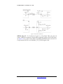
1
THE DINI GROUP LOGIC Emulation Source User Manual DNMEG_V5T_PCIE LOGIC EMULATION SOURCE DNMEG_V5T_PCIE User Manual Version 2.0 Date of Print March 26, 2009 The Dini Group 7469 Draper Ave. La Jolla, CA92037 Phone 858.454.3419 • Fax 858.454.1728 [email protected] www.dinigroup.com Copyright Notice and Proprietary Information Copyright © 2008 The Dini Group. All rights reserved. No part of this copyrighted work may be reproduced, modified or distributed in any form or by any means, without the prior written permission of The Dini Group. Right to Copy Documentation The Dini Group permits licensee to make copies of the documentation for its internal use only. Each copy shall include all copyrights, trademarks, disclaimers and proprietary rights notices. Disclaimer The Dini Group has made reasonable efforts to ensure that the information in this document is accurate and complete. However, The Dini Group assumes no liability for errors, or for any incidental, consequential, indirect, or special damages, including, without limitation, loss of use, loss or alteration of data, delays, or lost profits or savings, arising from the use of this document or the product which it accompanies. Table of Contents INTRODUCTION ............................................................................................................................................................................................................... 1 1 2 3 4 5 ABOUT THE DNMEG_V5T_PCIE DAUGHTER CARD ................................................................................................................................ 1 DNMEG_V5T_PCIE DAUGHTER CARD FEATURES .................................................................................................................................. 2 PACKAGE CONTENTS: ................................................................................................................................................................................ 3 INSPECT THE BOARD .................................................................................................................................................................................. 4 ADDITIONAL INFORMATION ....................................................................................................................................................................... 4 GETTING STARTED ........................................................................................................................................................................................................ 6 1 1.1 1.2 2 2.1 2.2 2.3 BEFORE YOU BEGIN ................................................................................................................................................................................... 6 Configuring the Programmable Components .................................................................................................................................................... 6 Warnings ........................................................................................................................................................................................................... 6 USING THE REFERENCE DESIGN ................................................................................................................................................................. 7 Initial Setup before Applying Power .................................................................................................................................................................. 7 Serial COM Setup using CRT ............................................................................................................................................................................ 8 Running the Reference Design ........................................................................................................................................................................... 8 PROGRAMMING/CONFIGURING THE HARDWARE............................................................................................................................................. 12 3 INTRODUCTION ........................................................................................................................................................................................ 12 Configuration Dip Switch ................................................................................................................................................................................ 12 4 CONFIGURATION OPTIONS ....................................................................................................................................................................... 13 4.1 Configuring the FPGA using JTAG ................................................................................................................................................................. 13 4.1.1 Setup ........................................................................................................................................................................................................ 13 4.1.2 Configuring the FPGA ............................................................................................................................................................................. 13 4.2 Configuring the FPGA using Master-Serial .................................................................................................................................................... 15 4.2.1 Setup ........................................................................................................................................................................................................ 15 4.2.2 Configuring the FPGA ............................................................................................................................................................................. 16 4.3 Configuring the FPGA using Master SPI......................................................................................................................................................... 17 4.3.1 Setup ........................................................................................................................................................................................................ 18 4.3.2 Configuring the FPGA ............................................................................................................................................................................. 18 3.1 HARDWARE DESCRIPTION ........................................................................................................................................................................................ 21 1 2 OVERVIEW ............................................................................................................................................................................................... 21 XILINX VIRTEX-5 FPGA .......................................................................................................................................................................... 23 2.1 Summary of Virtex-5 device features: .............................................................................................................................................................. 23 3 FPGA CONFIGURATION ........................................................................................................................................................................... 26 3.1 Configuration Dip Switch ................................................................................................................................................................................ 27 3.2 Master Serial Configuration ............................................................................................................................................................................ 27 3.3 Master Serial Peripheral Interface (SPI) Configuration.................................................................................................................................. 29 3.4 Slave SelectMAP Configuration....................................................................................................................................................................... 29 3.4.1 Slave SelectMAP Mictor Header ............................................................................................................................................................. 29 3.4.2 Slave SelectMAP Mictor connections to the FPGA ................................................................................................................................. 30 3.5 JTAG Configuration ........................................................................................................................................................................................ 31 3.5.1 In-System Programming PROM/JTAG Header ....................................................................................................................................... 32 3.5.2 JTAG connections to FPGA .................................................................................................................................................................... 32 4 CLOCK GENERATION................................................................................................................................................................................ 32 4.1 Clock Methodology .......................................................................................................................................................................................... 32 4.2 FPGA Clock Multiplier.................................................................................................................................................................................... 35 4.2.1 FPGA Clock Multiplier Circuit (U13) ..................................................................................................................................................... 36 4.2.2 Connections between the FPGA and Clock Multiplier ............................................................................................................................ 36 4.3 External FPGA Clock (LVDS) Input via SMA’s............................................................................................................................................... 37 4.3.1 External Clock Input Circuit .................................................................................................................................................................... 37 4.3.2 Connection between FPGA and External SMA Connectors .................................................................................................................... 37 4.4 DDR2 Clocking ............................................................................................................................................................................................... 38 4.4.1 DDR2 Oscillator (LVDS) Circuit ............................................................................................................................................................ 38 4.4.2 Clocking Connections between FPGA and DDR2 SDRAM SODIMM ................................................................................................... 38 4.5 RocketIO GTP Transceiver Clocking............................................................................................................................................................... 39 4.5.1 RocketIO GTP Transceiver Clock Multipliers ......................................................................................................................................... 40 4.5.2 RocketIO GTP Transceiver Clock (LVDS) Oscillators ........................................................................................................................... 40 4.5.3 RocketIO GTP Transceiver Oscillator Linear Power Supplies ................................................................................................................ 41 4.5.4 Clocking Connections between FPGA and GTP Clock Sources .............................................................................................................. 41 4.6 Daughter Card Clocks ..................................................................................................................................................................................... 42 4.6.1 Daughter Card Clock Circuit – Bottom Header (P2)................................................................................................................................ 42 4.6.2 Daughter Card Clock Circuit – Top Header (P1) ..................................................................................................................................... 43 4.6.3 Connections between the FPGA and the Daughter Card Header Clocks .................................................................................................. 43 5 LED INDICATORS ..................................................................................................................................................................................... 44 5.1 User LED’s ...................................................................................................................................................................................................... 44 5.2 Configuration DONE LED .............................................................................................................................................................................. 44 5.3 SFP Status LED’s ............................................................................................................................................................................................ 45 5.4 Power Supply Status LED’s ............................................................................................................................................................................. 45 6 MEMORY .................................................................................................................................................................................................. 45 6.1 DDR2 SDRAM ................................................................................................................................................................................................. 45 6.1.1 DDR2 Clocking ....................................................................................................................................................................................... 46 6.1.2 DDR2 Termination Scheme ..................................................................................................................................................................... 46 6.1.3 Digitally Controlled Impedance (DCI)..................................................................................................................................................... 48 6.1.4 On-Die Termination (ODT) ..................................................................................................................................................................... 49 6.1.5 VDD Switching Power Supply (P_SODIMM)........................................................................................................................................... 49 6.1.6 VTT Linear Power Supply (P0.9V_VTT) ................................................................................................................................................ 49 6.1.7 Serial Presence-Detect EEPROM Operation............................................................................................................................................ 49 6.1.8 DDR2 connections to FPGA .................................................................................................................................................................... 50 6.1.9 DDR2 PCB Trace Lengths....................................................................................................................................................................... 54 7 RS232 PORT............................................................................................................................................................................................. 54 7.1.1 Connections between FPGA and RS232 Port .......................................................................................................................................... 55 8 SERIAL FLASH ........................................................................................................................................................................................ 55 8.1.1 Connections between FPGA and Serial FLASH ...................................................................................................................................... 55 9 HIGH-SPEED SERIAL INTERFACES ............................................................................................................................................................ 56 9.1 GX Transceiver Clocks .................................................................................................................................................................................... 57 9.2 SMA Interface (x4)........................................................................................................................................................................................... 57 9.2.1 FPGA to SMA Connections..................................................................................................................................................................... 57 9.3 PCIE Cable Interface ...................................................................................................................................................................................... 58 9.3.1 Cable Reference Clocking Options .......................................................................................................................................................... 59 9.3.2 Selecting between Upstream or Downstream (Auxiliary Signals) ........................................................................................................... 61 9.3.3 Cable Present ........................................................................................................................................................................................... 61 9.3.4 Connections between FPGA and the PCIE Cable Connectors ................................................................................................................. 62 9.4 DisplayPort/SFP Interface .............................................................................................................................................................................. 63 9.4.1 Connections between FPGA and the DisplayPort Connectors ................................................................................................................. 64 9.4.2 Verilog Instantiations for AUX Channel LVDS Interface ....................................................................................................................... 65 9.4.3 SFP Pin Assignments ............................................................................................................................................................................... 66 9.4.4 Connections between FPGA and the SFP Connector ............................................................................................................................... 66 10 POWER DISTRIBUTION.............................................................................................................................................................................. 67 10.1 In-System Operation .................................................................................................................................................................................... 67 10.2 Stand Alone Operation................................................................................................................................................................................. 68 10.2.1 External Power Connector ....................................................................................................................................................................... 69 11 MICTOR HEADER ..................................................................................................................................................................................... 70 11.1.1 Mictor Header Circuit .............................................................................................................................................................................. 71 11.2 FPGA to Mictor Header .............................................................................................................................................................................. 71 12 DAUGHTER CARD HEADERS .................................................................................................................................................................... 73 12.1 Daughter Card clocking .............................................................................................................................................................................. 73 12.2 Daughter Card Header Pin Assignments ..................................................................................................................................................... 73 12.2.1 Special Pins on the Daughter Card Header .............................................................................................................................................. 76 12.3 VCCO Power Supply ...................................................................................................................................................................................... 76 12.4 FPGA to Daughter Card Header IO Connections ....................................................................................................................................... 77 12.5 Power and Reset .......................................................................................................................................................................................... 83 12.6 Insertion/Removal of Daughter Card ........................................................................................................................................................... 84 12.7 MEG Array Specifications ........................................................................................................................................................................... 86 13 MECHANICAL ........................................................................................................................................................................................... 87 13.1 Dimensions .................................................................................................................................................................................................. 87 APPENDIX 14 88 APPENDIX A: UCF FILE........................................................................................................................................................................... 88 List of Figures Figure 1 - DNMEG_V5T_PCIE Daughter Card ........................................................................................................................................................................................... 1 Figure 2 - DNMEG_V5T_PCIE Daughter Card Block Diagram.............................................................................................................................................................. 22 Figure 3 - Master Serial Mode Configuration ................................................................................................................................................................................................ 28 Figure 4 - Virtex-5 SPI Configuration Interface ........................................................................................................................................................................................... 29 Figure 5 – Slave SelectMAP Mictor Header .................................................................................................................................................................................................. 30 Figure 6 – JTAG Header ................................................................................................................................................................................................................................. 32 Figure 7 - Clocking Block Diagram ................................................................................................................................................................................................................ 33 Figure 8 - External Clock Input Circuit ......................................................................................................................................................................................................... 37 Figure 9 – DDR2 Oscillator (LVDS) Circuit ................................................................................................................................................................................................ 38 Figure 10 - RocketIO GTP Clock Multiplier Circuit.................................................................................................................................................................................... 40 Figure 11 - RocketIO GTP Oscillator Circuit ............................................................................................................................................................................................... 41 Figure 12 - GTP Transceiver Oscillator Linear Power Supplies Circuit .................................................................................................................................................... 41 Figure 13 - Daughter Card Header Clock Circuit, Bottom Header ............................................................................................................................................................ 43 Figure 14 - Daughter Card Clock Circuit, Top Header ................................................................................................................................................................................ 43 Figure 15 - SSTL18 Class I Termination ....................................................................................................................................................................................................... 47 Figure 16 – SSTL18 Class II Bidirectional Termination .............................................................................................................................................................................. 48 Figure 17 - VDD Switching Power Supply (P_SODIMM) ......................................................................................................................................................................... 49 Figure 18 - VTT Linear Power Supply (P0.9V_VTT) .................................................................................................................................................................................. 49 Figure 19 - RS232 Port..................................................................................................................................................................................................................................... 55 Figure 20 - Serial FLASH ................................................................................................................................................................................................................................ 55 Figure 21 - PCIE Clock Buffer ....................................................................................................................................................................................................................... 60 Figure 22 - Upstream to Downstream PCIE Ref Clock .............................................................................................................................................................................. 60 Figure 23 - Downstream to Upstream PCIE Ref Clock .............................................................................................................................................................................. 60 Figure 24 - PCIE1_CPRSNTn Signaling with Power Isolation .................................................................................................................................................................. 62 Figure 25 - Daughter Card Header Power (Optional) .................................................................................................................................................................................. 68 Figure 26 - ATX Power Supply....................................................................................................................................................................................................................... 69 Figure 27 - External Power Connection ........................................................................................................................................................................................................ 69 Figure 28 - 38 Pin Mictor Header ................................................................................................................................................................................................................... 71 Figure 29 - Daughter Card Interconnect Diagram ....................................................................................................................................................................................... 74 Figure 30 - Daughter Card Header Pin Assignments ................................................................................................................................................................................... 75 Figure 31 - VREF Daughter Card Header Signals ........................................................................................................................................................................................... 76 Figure 32 - VCCO Adjustable Linear Power Supplies ................................................................................................................................................................................. 77 Figure 33 - Daughter Card Header Power & RESET .................................................................................................................................................................................. 84 List of Tables Table 1 - Configuration Dip Switch ...............................................................................................................................................................................................................12 Table 2 - Configuration Dip Switch ...............................................................................................................................................................................................................27 Table 3 – Virtex-5 Uncompressed .rbf File Size ...........................................................................................................................................................................................28 Table 4 – Slave SelectMAP Mictor connections to the FPGA....................................................................................................................................................................30 Table 5 - JTAG connections to the PROM/FPGA .....................................................................................................................................................................................32 Table 6 - Clocking inputs to the FPGA‘s.......................................................................................................................................................................................................34 Table 7 - Connections between FPGA and Clock Multiplier ......................................................................................................................................................................37 Table 8 - Connection between FPGA and External SMA Connectors......................................................................................................................................................38 Table 9 - Connections between FPGA and the DDR2 SDRAM SODIMM ............................................................................................................................................38 Table 10 - GTP Oscillator Frequency Select .................................................................................................................................................................................................40 Table 11 - Connections between FPGA and GTP Clock Sources .............................................................................................................................................................41 Table 12 - Connections between FPGA and Daughter Card Header Clocks ...........................................................................................................................................43 Table 13 – User LED‘s ....................................................................................................................................................................................................................................44 Table 14 – FPGA_DONE LED ....................................................................................................................................................................................................................45 Table 15 – SFP LED Indicator .......................................................................................................................................................................................................................45 Table 16 – Power Supply Status LED‘s .........................................................................................................................................................................................................45 Table 17 - DDR2 Termination Scheme .........................................................................................................................................................................................................46 Table 18 - Serial Presence-Detect EEPROM Connections .........................................................................................................................................................................50 Table 19 - Connections between the FPGA and the DDR2 SODIMM ....................................................................................................................................................50 Table 20 – DDR2 PCB Trace Lengths ..........................................................................................................................................................................................................54 Table 21 - Connections between FPGA and the RS232 Port .....................................................................................................................................................................55 Table 22 - Connections between FPGA and the Serial FLASH .................................................................................................................................................................56 Table 23 - Connections between FPGA and SMA Connectors ..................................................................................................................................................................57 Table 24 - Connections between FPGA and the PCIE Cable Connectors ...............................................................................................................................................62 Table 25 - Connections between FPGA and the DisplayPort Connectors ...............................................................................................................................................64 Table 26 – SFP Pin Assignments ....................................................................................................................................................................................................................66 Table 27 - Connections between FPGA and the SFP Connector...............................................................................................................................................................66 Table 28 - Connections between FPGA and Mictor Header ......................................................................................................................................................................71 Table 29 - FPGA to Daughter Card Header IO Connections ....................................................................................................................................................................77 Table 30 – Daughter Card Reset Signal (DC_RSTn) ...................................................................................................................................................................................84 1 Chapter I N T R O D U C T I O N Introduction This User Manual accompanies the DNMEG_V5T_PCIE Daughter Card. For specific information regarding the Virtex-5 parts, please reference the datasheet on the Xilinx website. 1 About the DNMEG_V5T_PCIE Daughter Card The DNMEG_V5T_PCIE Daughter Card provides a complete development platform for designing and verifying applications based on the Xilinx Virtex-5 FPGA family. This board allows designers to implement high-speed applications using the RocketIO GTP Transceivers available on the LXT/SXT/FXT parts. The DNMEG_V5T_PCIE Daughter Card can operate in standalone mode or in conjunction with one of the Dini products that houses a 400 pin MEG-Array Daughter card header, e.g. DN9000K10PCI. Figure 1 - DNMEG_V5T_PCIE Daughter Card DNMEG_V5T_PCIE User Manual www.dinigroup.com 1 I N T R O D U C T I O N 2 DNMEG_V5T_PCIE Daughter Card Features DNMEG_V5T_PCIE Daughter Card features the following: Single Xilinx Virtex-5 FPGA (FF1136), -1, -2, -3 Speed Grade o XC5VLX50T, XC5VLX85T, XC5VLX110T, XC5VLX155T o XC5VSX50T, XC5VSX95T o XC5VFX70T, XC5VFX100T Flexible Clock Resources o FPGA Clock Multiplier (Si5326) o External FPGA Clock (LVDS) Input via SMA‘s (x1) o DDR2 Clock Oscillator o GTP Transceiver Clock Multipliers - Si5326 (x1) o GTP Transceiver Clock (LVDS) Oscillators (x2) o Multiple clocks from the Daughter Card Headers (P1, P2) FPGA Configuration o Master-serial configuration mode o Master Serial Peripheral Interface (SPI) configuration mode o Slave SelectMAP (parallel) configuration mode (x8, x16), using the Mictor interface o JTAG/Boundary-Scan configuration mode o DIP Switch to select Configuration Mode Memory o DDR2, 512MB (64Meg x 64), 200pin SODIMM (PC2-4200), support up to 4GB o Serial FLASH Memory, 16Mbit (4096 pages of 512/528 bytes/page) DNMEG_V5T_PCIE User Manual www.dinigroup.com 2 I N T R O D U C T I O N High-Speed Transceiver Channels o DisplayPort/SFP Interface (see note) o Differential SMA (50 ohm) Channels (x4) o PCI Express Cable (x4) User LED‘s (x8) Onboard distributed Power Supplies Daughter Card Headers (x2) LVDS – MEG-Array (400 pin) interface to DN8000xxx/DN9000xxx products Full support for embedded Logic Analyzers o ChipScopeTM Pro Analyzer RS232 Port, 10 pin Header – MicroBlaze Applications Stand Alone operation, requires an external +12V/+5V ATX power supply Note: DisplayPort and SFP interfaces are only available on the larger parts; XC5VLX110T, XC5VLX155T, XC5VSX95T, XC5VFX70T, and XC5VFX100T. 3 Package Contents: Before using the kit or installing the software, be sure to check the contents of the kit and inspect the board to verify that you received all of the items. If any of these items are missing, contact The Dini Group before you proceed. The DNMEG_V5T_PCIE Daughter Card kit includes the following: RS232 IDC Header to Female DB9 Cable Assembly RS232 Serial Cable Assembly, 6ft, F/F (DB9) iPass PCIe x4 Cable Assembly, 28 AWG, 2.00m CD ROM containing: o Virtex-5 Reference Design (Verilog) o User Manual (pdf format) DNMEG_V5T_PCIE User Manual www.dinigroup.com 3 I N T R O D U C T I O N o Schematic (pdf format) o Component Datasheets (pdf format) Optional items that support development efforts (not provided): Xilinx ISE software and Xilinx Platform Cable USB download cable DDR2 SODIMM (Available upon request) SMA, DisplayPort Cables, Loopback Test Cables (Available upon request) 4 Inspect the Board Place the board on an anti-static surface and inspect it to ensure that it has not been damaged during shipment. Verify that all components are on the board and appear intact. 5 Additional Information For additional information, please visit http://www.dinigroup.com/. The following table lists some of the resources you can access from this website. You can also directly access these resources using the provided URLs. Resource Description/URL User Manual This is the main source of technical information. The manual should contain most of the answers to your questions Demonstration Videos MEG-Array Daughter Card header insertion and removal video Dini Group Web Site The web page will contain the latest user manual, application notes, FAQ, articles, and any device errata and manual addenda. Please visit and bookmark: http://www.dinigroup.com Data Book Pages from Virtex-5 Databook, which contains device-specific information on Xilinx device characteristics E-Mail You may direct questions and feedback to the Dini Group using this e-mail address: [email protected] Phone Support Call us at 858.454.3419 during the hours of 8:00am to 5:00pm Pacific Time. DNMEG_V5T_PCIE User Manual www.dinigroup.com 4 I N T R O D U C T I O N Resource FAQ Description/URL The download section of the web page may contain a document called DNMEG_V5T_PCIE Frequently Asked Questions (FAQ). This document is periodically updated with information that may not be in the User‘s Manual. DNMEG_V5T_PCIE User Manual www.dinigroup.com 5 G E T T I N G 2 Chapter S T A R T E D Getting Started Congratulations on your purchase of the DNMEG_V5T_PCIE Daughter Card. The remainder of this chapter describes how to start using the board. 1 Before You Begin 1.1 Configuring the Programmable Components The DNMEG_V5T_PCIE Daughter Card has been factory tested and preprogrammed to ensure correct operation. The user does not need to alter any jumpers or program anything to see the board work. 1.2 Warnings Daughter Card Test Headers (Over Voltage) - The 400-pin daughter card test headers are NOT 5V tolerant. Take care when handling the board to avoid touching the components and daughter card connections due to ESD. ESD Warning - The board is sensitive to static electricity, so treat the PCB accordingly. The target markets for this product are engineers that are familiar with FPGAs and circuit boards. However, if needed, the following web page has an excellent tutorial on the ―Fundamentals of ESD‖ for those of you who are new to ESD sensitive products: http://www.esda.org/basics/part1.cfm Operating Temperature - Avoid touching the PTH012050WAZ power supply modules (PSU1, PSU2, and PSU3) as they operate at high temperatures and may cause skin burns. DNMEG_V5T_PCIE User Manual www.dinigroup.com 6 G E T T I N G S T A R T E D 2 Using the Reference Design The Dini Group provides a reference design for the DNMEG_V5T_PCIE to help the user get started with building applications: MainTest – Described in this document, allows the user to test all the interfaces on the board. 2.1 Initial Setup before Applying Power Attach the ATX Power Supply to the power header (J31) on the DNMEG_V5T_PCIE Daughter Card. Connect the ―Xilinx Platform Cable USB‖ from the Test PC to the JTAG header (J2). Connect the serial cable from the Test PC to the RS232 header (J14). Ensure that pin 1 location of the cable aligns with pin 1 location on the PCB. Connect the iPASS connectors, J3 -> J4, using the iPASS cable. Optional: Install the DD2 SODIMM module in SODIMM socket (J30). Connect the SMA Coax cables from J8 –> J7, J10 –> J9, and repeat for all four channels. Connect the DisplayPort connectors, J1 -> J11, using the DisplayPort cable. Install the SFP loopback connector in the SFP connector (J6). Note: Various Loop-back cables may be required if the user intends to exercise the RocketIO interfaces. These cables are not provided as part of the Kit. DNMEG_V5T_PCIE User Manual www.dinigroup.com 7 G E T T I N G S T A R T E D 2.2 Serial COM Setup using CRT Connect the RS232 Serial cable to a COM port on the host computer and the RS232 header (J14) on the DNMEG_V5T_PCIE Daughter Card. Configure CRT to the following settings: Warning: If using HyperTerminal, the text in the buffer window (the window above the command window) may appear to be corrupted. The text in the command window should move to the buffer window as the text scrolls past the top line in the command window. However, the text may appear in the buffer window with missing characters or extra characters. See Microsoft Help and Support, article ID: 274261 2.3 Running the Reference Design This section lists detailed instructions for executing the reference design. Power-Up the DNMEG_V5T_PCIE Daughter Card, open a CRT Window and perform the following steps; 1. Periods will be displayed when the DNMEG_V5T_PCIE is first powered ON. Press ―ENTER‖ in the CRT Window to display the ―DNMEG_V5T_PCIE Main Menu‖. DNMEG_V5T_PCIE User Manual www.dinigroup.com 8 G E T T I N G S T A R T E D 2. Verify that the FPGA configured successfully (the Blue LED (DS17) will turn ON). The CRT screen will display periods, press ―ENTER‖ in the CRT window to display the ―DNMEG_V5T_PCIE Main Menu‖. 3. Select test option ‗a‘, ―DDR2 Test‖ in the CRT window and verify that the test PASS (periods will be displayed as the memory locations are being tested, if no DDR2 Module is present, the test will display read/write errors). Press ―ENTER‖ to stop the test. 4. Select test option ‗b‘, ―SPI FLASH Test‖ in the CRT window and verify that the test PASSED. DNMEG_V5T_PCIE User Manual www.dinigroup.com 9 G E T T I N G S T A R T E D 5. Select test option ‗c‘, ―Temperature Sensor Test‖ in the HyperTerminal window and verify that the test returns the FPGA temperature. DNMEG_V5T_PCIE User Manual www.dinigroup.com 10 G E T T I N G S T A R T E D 6. Select test option ‗e‘, ―RocketIO GTP Test – start/restart‖ in the CRT window. This will start the test; proceed to test option ‗f‘ to view the results. 7. Select test option ‗f‘, ―RocketIO GTP Test – show status‖ in the CRT window to view the results. Please reference the CUSTOMER CD for code examples. The next section describes configuring and programming the hardware in detail. DNMEG_V5T_PCIE User Manual www.dinigroup.com 11 P R O G R A M M I N G / C O N F I G U R I N G T H E 3 Chapter H A R D W A R E Programming/Configuring the Hardware This chapter details the programming and configuration instructions for the DNMEG_V5T_PCIE Daughter Card. 3 Introduction Virtex-5 devices are configured by loading application-specific configuration data—the bitstream—into internal memory. Because Xilinx FPGA configuration memory is volatile, it must be configured each time it is powered-up. The bitstream is loaded into the device through special configuration pins. These configuration pins serve as the interface for a number of different configuration modes (the following configuration options are supported on this board): JTAG/Boundary-Scan Master-Serial Master Serial Peripheral Interface (SPI) Slave SelectMAP (parallel) configuration mode (x8, x16), using the Mictor interface 3.1 Configuration Dip Switch A dip switch is provided to select the configuration mode, see Table 1: Dip Switch (S4) is not used and is connected to the FPGA (U21.AG15), available to the user. Table 1 - Configuration Dip Switch Configuration Mode Master Serial DNMEG_V5T_PCIE User Manual M[2:0] 000 www.dinigroup.com Dip Switch Setting (S4) 3, 2, and 1 ON 12 P R O G R A M M I N G / C O N F I G U R I N G Configuration Mode Master SPI JTAG Slave SelectMAP T H E M[2:0] 001 101 110 H A R D W A R E Dip Switch Setting (S4) 3, 2 ON and 1 OFF 3, 1 OFF and 2 ON 3, 2 OFF and 1 ON 4 Configuration Options This section lists detailed instructions for programming the Xilinx Virtex-5 FPGA using iMPACT, Version 10.1 tools. Before configuring the FPGA, ensure that the Xilinx software and the ―Xilinx Platform Cable USB‖ driver software are installed on the host computer. Note: This User Manual will not be updated for every revision of the Xilinx ISE tools, so please be aware of minor differences. 4.1 Configuring the FPGA using JTAG The JTAG/Boundary-Scan configuration interface is always available, regardless of the Mode pin settings. The JTAG/Boundary-Scan configuration mode disables all other configuration modes to prevent conflicts between configuration interfaces. 4.1.1 Setup Before configuring the FPGA, ensure the following steps have been completed: 1. Attach an ATX Power Supply to the Power header (J31) on the DNMEG_V5T_PCIE Daughter Card. 2. Connect the ―Xilinx Platform Cable USB‖ to the ―JTAG‖ header (J2). 3. Power up the board by turning ON the ATX power supply and verify the P12V LED (DS6) is ON indicating the presence of +12V (located next to the JTAG header). 4.1.2 Configuring the FPGA To configure the Xilinx FPGA, perform the following steps: 1. Open iMPACT and create a new default project. Select ―Configure devices using Boundary-Scan (JTAG)‖ from the iMPACT welcome menu. DNMEG_V5T_PCIE User Manual www.dinigroup.com 13 P R O G R A M M I N G / C O N F I G U R I N G T H E H A R D W A R E 2. iMPACT will identify the PROM (XCF32P) and the FPGA (XC5VLX110T – depends on the build option) in the JTAG chain. A pop-up window will display ―Assign New Configuration File‖. Click ―Bypass‖ and specify the location for the FPGA bit file based on the type of FPGA populated e.g. XC5VLX110T; ―CUST_CD\DiniProducts\DN_BITFILES\DNMEG_V5T_PCIE\MainTest\LX110T_RE V2\ LX110T\fpga.bit‖ Select Device 2 in the ―Device Programming Properties‖ window and click ―OK‖ to continue. DNMEG_V5T_PCIE User Manual www.dinigroup.com 14 P R O G R A M M I N G / C O N F I G U R I N G T H E H A R D W A R E 3. Right-click on the FPGA and select the ―Program‖ option. A ―Progress Dialog‖ box will appear indicating programming progress. 4. The activation of the ―CFG DONE‖ blue LED (DS17) indicates that the FPGA configured successfully. 4.2 Configuring the FPGA using Master-Serial The Master-Serial mode is designed so that the FPGA can be configured from a Xilinx Flash PROM. The DNMEG_V5T_PCIE Daughter Card is populated with an XCF32P, 32Mbit Flash PROM. This allows the user to configure the following parts: XC5VLX50T, XC5VLX85T, XC5VLX110T XC5VSX50T XC5VFX70T 4.2.1 Setup Before configuring the FPGA, ensure the following steps have been completed: 1. Attach an ATX Power Supply to the Power header (J31) on the DNMEG_V5T_PCIE Daughter Card. DNMEG_V5T_PCIE User Manual www.dinigroup.com 15 P R O G R A M M I N G / C O N F I G U R I N G T H E H A R D W A R E 2. Connect the ―Xilinx Platform Cable USB‖ to the ―JTAG‖ header (J2). 3. Set the Configuration Dip Switch (S4) as shown below: Configuration Mode Master-Serial M[2:0] 000 Dip Switch Setting (S4) 3, 2, and 1 ON 4. Power up the board by turning ON the ATX power supply and verify the P12V LED (DS6) is ON indicating the presence of +12V (located next to the JTAG header). 4.2.2 Configuring the FPGA To configure the Xilinx Flash PROM, perform the following steps: 1. Open iMPACT and create a new default project. Select ―Configure devices using Boundary-Scan (JTAG)‖ from the iMPACT welcome menu. 2. iMPACT will identify the PROM (XCF32P) and the FPGA (XC5VLX110T – depends on the build option) in the JTAG chain. A pop-up window will DNMEG_V5T_PCIE User Manual www.dinigroup.com 16 P R O G R A M M I N G / C O N F I G U R I N G T H E H A R D W A R E display ―Assign New Configuration File‖. Specify the PROM file location for the type of FPGA populated e.g. XC5VLX110T; ―CUST_CD\DiniProducts\DN_BITFILES\DNMEG_V5T_PCIE\MainTest\LX110T_RE V2\fpga.mcs‖ Select ―Bypass‖ for the FPGA and click ―OK‖ in the ―Device Programming Properties‖ window to continue. 3. Right-click on the XCF32P device and select ―Program‖. A Process Dialog box will indicate programming progress. 4. Power-cycle the DNMEG_V5T_PCIE Daughter Card and verify that the ―FPGA DONE‖ blue LED (DS17) is enabled, indicating successful configuration of the FPGA. Note: Configuring the FPGA from the PROM takes a while to complete. 4.3 Configuring the FPGA using Master SPI In Master SPI Serial Flash Mode, the Virtex-5 FPGA configures itself from an attached industry-standard SPI Serial Flash PROM. The DNMEG_V5T_PCIE Daughter Card DNMEG_V5T_PCIE User Manual www.dinigroup.com 17 P R O G R A M M I N G / C O N F I G U R I N G T H E H A R D W A R E is populated with a ST Micro, M25P128, 128Mbit Serial Flash PROM. This allows the user to configure the following parts: XC5VLX155T XC5VSX95T XC5VFX100T 4.3.1 Setup Before configuring the FPGA, ensure the following steps have been completed: 1. Attach an ATX Power Supply to the Power header (J31) on the DNMEG_V5T_PCIE Daughter Card. 2. Connect the ―Xilinx Platform Cable USB‖ to the ―JTAG‖ header (J2). 3. Set the Configuration Dip Switch (S4) as shown below: Configuration Mode Master SPI M[2:0] 001 Dip Switch Setting (S4) 3, 2 ON and 1 OFF 4. Power up the board by turning ON the ATX power supply and verify the P12V LED (DS6) is ON indicating the presence of +12V (located next to the JTAG header). 4.3.2 Configuring the FPGA To configure the Serial Flash PROM, perform the following steps: 1. Open iMPACT and create a new default project. Select ―Configure devices using Boundary-Scan (JTAG)‖ from the iMPACT welcome menu. DNMEG_V5T_PCIE User Manual www.dinigroup.com 18 P R O G R A M M I N G / C O N F I G U R I N G T H E H A R D W A R E 2. iMPACT will identify the FPGA (XC5VFX100T – depends on the build option) in the JTAG chain. A pop-up window will display ―Assign New Configuration File‖. Click ―Cancel‖ followed by ―OK‖ to continue. 3. Right-click on the FPGA and select ―Add SPI Device‖ option. Specify the file location for the PROM file based on the type of FPGA populated e.g. XC5VFX100T; ―CUST_CD\ DiniProducts\DN_BITFILES\DNMEG_V5T_PCIE\MainTest\ LX155T_REV2\fpga.mcs‖ 4. Select the M25P128 device in the ―Select Device Part Name‖ window. DNMEG_V5T_PCIE User Manual www.dinigroup.com 19 P R O G R A M M I N G / C O N F I G U R I N G T H E H A R D W A R E 5. Right-Click on the ―FLASH‖ icon and select ―Program‖. A Process Dialog box will indicate programming progress. 6. Power-cycle the DNMEG_V5T_PCIE Daughter Card and verify that the ―FPGA DONE‖ blue LED (DS17) is enabled, indicating successful configuration of the FPGA. Note: Configuring the FPGA from the PROM takes a while to complete. Please reference the Xilinx website for more information on how to program and configure the Xilinx parts. The next section describes the hardware in detail. DNMEG_V5T_PCIE User Manual www.dinigroup.com 20 H A R D W A R E 4 Chapter D E S C R I P T I O N Hardware Description This chapter describes the functional blocks of the design and focuses on the Hardware. 1 Overview The DNMEG_V5T_PCIE Daughter Card provides for a comprehensive collection of peripherals to use in creating a system around the Xilinx Virtex-5 FPGA. A high level block diagram of the DNMEG_V5T_PCIE Daughter Card is shown in Figure 2, followed by a brief description of each section. The DNMEG_V5T_PCIE Daughter Card provides several high-speed serial interfaces utilizing the Virtex-5 GTP/GTX Transceivers. The board provides four high-speed SMA channels allowing up to 3.75Gbps LVDS serial links. The board also provides two PCIe (x4) interfaces, one configured ―To Host‖ and one as ―From Host‖ with iPASS connectors. A Display Port (Source/Sink) interface was provided for the remaining GTP interfaces. A Small-factor Pluggable (SFP) connector shared with one of the DisplayPort channels allows for Gigabit Ethernet or Fiber channel interfaces. External memory to the FPGA is realized using a 64 bit, 200 pin SODIMM (PC-4200). The 400 pin MEG-Array connector on the bottom of the printed circuit board assembly (PCBA) is used to interface to the Dini Group products, e.g. DN9000K10PCI. The 400 pin MEG-Array connector on the top of the PCBA can be used for IO expansion utilizing the DNMEG_Obs Daughter Card. Numerous clocking options exists to allow the user a flexible clocking scheme. The FPGA is configured using the ―Xilinx Platform Cable USB‖ to program the configuration PROM (XCF32P), and FPGA via JTAG. The FPGA can also be configured from a an external source via Slave SelectMAP and the Mictor Interface. In standalone mode, the DNMEG_V5T_PCIE Daughter Card receives power from an external +12V/+5V ATX power supply. An RS232 interface exists to allow communication with the application. LED‘s are used to indicate configuration status, power supply presence and eight LED‘s are provided for the user. DNMEG_S2GX User Manual www.dinigroup.com 21 +3.3V PSU +2.5V +5.0V +12V LED0 LED2 LED3 +5V SFP (20Pin) www.dinigroup.com LED6 x4 x4 GTP CLK CIRCUIT OSC (x2) SYNTH (x2) EXT SMA (x2) x4 MICTOR Logic Analyzer/ Slave SelectMAP RS232 PORT 10-Pin XILINX VIRTEX-5 FPGA +5V @ 4A +12V @ 4A +3.3V @ 6A SPI SERIAL FLASH M25P128 CONFIGURATION PROM XCFP32P Note: RED indicates functionality only available on the larger parts; XC5VLX110T, XC5VLX155T, XC5VSX95T, XC5VFX70T, and XC5VFX100T x2 LED7 x4 LED8 FAN PWR OSC 200MHz 17/11 X4 Sink 14.5mm x 17.4mm LED5 x1 SERIALFLASH 16 Mbit AT45DB161D DDR-II SODIMM 2GB (200PIN) 123 x4 DisplayPort (20Pin) x4 DisplayPort 14.5mm x 17.4mm (20Pin) 38.8mm x 26.4mm x4 iPASS (38Pin) (38Pin) x4 iPASS x 26.4mm 38.8mm 41.3mm x 16.25mm LED4 x2 +1.8V/2.5V/3.3V +1.0V LED1 x1 SFP & Status LEDs @ 6A 1.8V PSU 1.8V @ 6A 1.8V @ 6A PTH12050 PTH12050 PTH12050 PSU PSU 1.0V @ 16A PTH08T220WAZ 4 X4 Source x4 SMA +VBATT BATT CONN +5V +12V AUX HDD PWR CONNECTOR DAUGHTER CARD (TOP) STATUS LED'S 4 JTAG 2mm Note: SPI Serial Flash used for; XC5VLX155T, XC5VSX95T, and XC5VFX100T MEG Array – Plug (400 Pin) 84520-102LF PWR STATUS INDICATORS DAUGHTER CARD (BOT) DNMEG_V5T_PCIE User Manual MEG Array – Receptacle (400 Pin) 74390-101LF H A R D W A R E D E S C R I P T I O N Figure 2 - DNMEG_V5T_PCIE Daughter Card Block Diagram 22 H A R D W A R E D E S C R I P T I O N 2 Xilinx Virtex-5 FPGA The Virtex-5 family provides the newest most powerful features in the FPGA market. Using the second generation ASMBL (Advanced Silicon Modular Block) columnbased architecture, the Virtex-5 family contains four distinct platforms (sub-families), the most choice offered by any FPGA family. Each platform contains a different ratio of features to address the needs of a wide variety of advanced logic designs. This overview contains detailed information about the LX, LXT, and SXT platforms. In addition to the most advanced, high-performance logic fabric, Virtex-5 FPGAs contain many hard-IP system level blocks, including powerful 36-Kbit block RAM/FIFOs, second generation 25 x 18 DSP slices, SelectIO™ technology with built-in digitallycontrolled impedance, ChipSync™ source-synchronous interface blocks, system monitor functionality, enhanced clock management tiles with integrated DCM (Digital Clock Managers) and phase-locked-loop (PLL) clock generators, and advanced configuration options. The LXT and SXT devices also contain power-optimized highspeed serial transceiver blocks for enhanced serial connectivity, a PCI Express™ compliant built-in Endpoint block, and tri-mode Ethernet MACs (Media Access Controllers). These features allow advanced logic designers to build the highest levels of performance and functionality into their FPGA-based systems. Built on a 65-nm state-of-the-art copper process technology, Virtex-5 FPGAs are a programmable alternative to custom ASIC technology. Most advanced system designs require the programmable strength of FPGAs. Virtex-5 FPGAs offer the best solution for addressing the needs of high-performance logic designers, high-performance DSP designers, and high-performance embedded systems designers with unprecedented logic, DSP, hard/soft microprocessor, and connectivity capabilities. The Virtex-5 LXT, SXT, and FXT platforms include advanced high-speed serial connectivity and link/transaction layer capability. 2.1 Summary of Virtex-5 device features: Four platforms LX, LXT, SXT, and FXT o Virtex-5 LX: High-performance general logic applications o Virtex-5 LXT: High-performance logic with advanced serial connectivity o Virtex-5 SXT: High-performance signal processing applications with advanced serial connectivity o Virtex-5 FXT: High-performance embedded systems with advanced serial connectivity Cross-platform compatibility DNMEG_V5T_PCIE User Manual www.dinigroup.com 23 H A R D W A R E D E S C R I P T I O N o LXT, SXT, and FXT devices are footprint compatible in the same package Most advanced, high-performance, optimal-utilization, FPGA fabric o Real 6-input look-up table (LUT) technology o Dual 5-LUT option o Improved reduced-hop routing o 64-bit distributed RAM option o SRL32/Dual SRL16 option Powerful clock management tile (CMT) clocking o Digital Clock Manager (DCM) blocks for zero delay buffering, frequency synthesis, and clock phase shifting o PLL blocks for input jitter filtering, zero delay buffering, frequency synthesis, and phase-matched clock division 36-Kbit block RAM/FIFOs o True dual-port RAM blocks o Enhanced optional programmable FIFO logic o Programmable True dual-port widths up to x36 o Simple dual-port widths up to x72 o Built-in optional error-correction circuitry o Optionally program each block as two independent 18-Kbit blocks 65-nm copper CMOS process technology 1.0V core voltage High signal-integrity flip-chip packaging available in standard or Pb-free package options High-performance parallel SelectIO technology DNMEG_V5T_PCIE User Manual www.dinigroup.com 24 H A R D W A R E D E S C R I P T I O N o 1.2V to 3.3V I/O Operation o Source-synchronous interfacing using ChipSync technology o Digitally-controlled impedance (DCI) active termination o Flexible fine-grained I/O banking o High-speed memory interface support Advanced DSP48E slices o 25 x 18, two‘s complement, multiplication o Optional adder, subtracter, and accumulator o Optional pipelining o Optional bitwise logical functionality o Dedicated cascade connections Flexible configuration options o SPI and Parallel FLASH interface o Multi-bitstream support with dedicated fallback reconfiguration logic o Auto bus width detection capability Built-In Endpoint blocks for PCI Express (LXT/SXT) o Compliant with the PCI Express Base Specification 1.1 o x1, x2, x4, or x8 lane support per block o Works in conjunction with RocketIO™ transceivers Tri-mode 10/100/1000 Mb/s Ethernet MACs (LXT/SXT) o RocketIO transceivers can be used as PHY or connect to external PHY using many soft MII (Media Independent Interface) options RocketIO GTP transceivers 100 Mb/s to 3.75 Gb/s (LXT/SXT) System Monitoring capability on all devices DNMEG_V5T_PCIE User Manual www.dinigroup.com 25 H A R D W A R E D E S C R I P T I O N o On-chip/Off-chip thermal monitoring o On-chip/Off-chip power supply monitoring o JTAG access to all monitored quantities 3 FPGA Configuration Virtex-5 devices are configured by loading application-specific configuration data—the bitstream—into internal memory. Because Xilinx FPGA configuration memory is volatile, it must be configured each time it is powered-up. The bitstream is loaded into the device through special configuration pins. These configuration pins serve as the interface for a number of different configuration modes (the following are supported on this board): Master-Serial Master Serial Peripheral Interface (SPI) Slave SelectMAP (parallel) configuration mode (x8, x16), using the Mictor interface JTAG/Boundary-Scan The specific configuration mode is selected by setting the appropriate level on the dedicated Mode input pins M[2:0]. The terms Master and Slave refer to the direction of the configuration clock (CCLK): In Master configuration modes, the Virtex-5 device drives CCLK from an internal oscillator. To get the desired frequency, BitGen -g ConfigRate is used. The ―BitGen‖ section of the Development System Reference Guide provides more information. In Slave configuration modes, CCLK is an input. The JTAG/Boundary-Scan configuration interface is always available, regardless of the Mode pin settings. The JTAG/Boundary-Scan configuration mode disables all other configuration modes to prevent conflicts between configuration interfaces. Certain pins are dedicated to configuration, while others are dual-purpose, see datasheet. Dualpurpose pins serve both as configuration pins and as user I/O after configuration. Dedicated configuration pins retain their function after configuration. Configuration constraints can be selected when generating the Virtex-5 bitstream. Certain configuration operations can be affected by these constraints. For a description of the available constraints, see the software constraints guide. DNMEG_V5T_PCIE User Manual www.dinigroup.com 26 H A R D W A R E D E S C R I P T I O N 3.1 Configuration Dip Switch A dip switch (S4) is provided to select the configuration option, see Table 2: Dip Switch (S4) is not used and is connected to the FPGA (U21.AG15), available to the user. Table 2 - Configuration Dip Switch Configuration Mode Master Serial Master Serial JTAG Slave SelectMAP M[2:0] 000 001 101 Dip Switch Setting (S4) 3, 2, and 1 ON 3, 2 ON and 1 OFF 3, 1 OFF and 2 ON 110 3, 2 OFF and 1 ON 3.2 Master Serial Configuration Master Serial configuration mode (shown in Figure 3) is most commonly used with configuration PROMs, because it is simple to implement. Only a small number of signals are required to interface the PROM with the FPGA, and an external clock source is not required for configuration. In FPGA Master Serial mode, the FPGA generates the configuration clock. In this mode, data is available on the PROM Data (D0) pin when CF is HIGH, and CE and OE are enabled. New data is available a short access time after each rising clock edge. DNMEG_V5T_PCIE User Manual www.dinigroup.com 27 H A R D W A R E D E S C R I P T I O N Figure 3 - Master Serial Mode Configuration Table 3 shows the uncompressed configuration file size for the Virtex-5 devices. Table 3 – Virtex-5 Uncompressed .rbf File Size Device XC5VLX50T XC5VLX85T XC5VLX110T XC5VLX155T Data Size (Bits) 14,052,352 23,341,312 31,118,848 43,042,304 PROM/Flash XCF32P XCF32P XCF32P M25P128 XC5VSX50T XC5VSX95T 20,019,328 35,716,096 XCF32P M25P128 XC5VFX70T 27,025,408 XCF32P XC5VFX100T 39,389,696 M25P128 Note: Master-Serial configuration mode is not available for the devices listed in red. A Serial Flash option is required to configure the lager parts using Master SPI configuration mode. DNMEG_V5T_PCIE User Manual www.dinigroup.com 28 H A R D W A R E D E S C R I P T I O N 3.3 Master Serial Peripheral Interface (SPI) Configuration In SPI serial Flash mode, M[2:0]=001. The Virtex-5 FPGA configures itself from an attached industry-standard SPI serial Flash PROM. Although SPI is a standard fourwire interface, various available SPI Flash memories use different read commands and protocol. Besides M[2:0], FS[2:0] pins are sampled by the INIT_B rising edge to determine the type of read commands used by SPI Flash. For Virtex-5 FPGA configurations, the default address always starts from 0. Figure 4 shows the SPI related configuration pins, and the standard connection between Virtex-5 devices and SPI Flash. Figure 4 - Virtex-5 SPI Configuration Interface See XAPP951 – Configuring Xilinx FPGAs with SPE Serial Flash application note for more information. Note: Since the SPI Serial Flash (U57) share signals with the Serial Flash (U15), enable write protect signal FLASH_Wn (U1.J12) during normal operation. 3.4 Slave SelectMAP Configuration In order to configure the DNMEG_V5T_PCIE Daughter Card from externally other Dini products, a Slave SelectMAP configuration interface (8/16-bit configuration bus ―FPGA_MICTOR_D[15..0]_EVEN‖) is provided to the Virtex-5 FPGA (U21) via the Mictor header (J17). The bus width of SelectMAP is automatically detected. In Slave SelectMAP, ―FPGA_CCLK‖ is an input and must be supplied by the configuration source. Zero ohm resistors are provided to isolate the Mictor header (J17) from the configuration signals if the header is used for debug/trace functions. 3.4.1 Slave SelectMAP Mictor Header Figure 5 shows the pin assignments for the Slave SelectMAP Mictor header. DNMEG_V5T_PCIE User Manual www.dinigroup.com 29 H A R D W A R E D E S C R I P T I O N P2.5VD R151 (DNI-0R) R152 (DNI-0R) J17 MICTOR_VDC_NC MICTOR_GND_NC FPGA_MICTOR_CLK_EVEN FPGA_MICTOR_D15_EVEN FPGA_MICTOR_D14_EVEN FPGA_MICTOR_D13_EVEN FPGA_MICTOR_D12_EVEN FPGA_MICTOR_D11_EVEN FPGA_MICTOR_D10_EVEN FPGA_MICTOR_D9_EVEN FPGA_MICTOR_D8_EVEN FPGA_MICTOR_D7_EVEN FPGA_MICTOR_D6_EVEN FPGA_MICTOR_D5_EVEN FPGA_MICTOR_D4_EVEN FPGA_MICTOR_D3_EVEN FPGA_MICTOR_D2_EVEN FPGA_MICTOR_D1_EVEN FPGA_MICTOR_D0_EVEN 1 3 5 7 9 11 13 15 17 19 21 23 25 27 29 31 33 35 37 39 40 41 Silkscreen: "MICTOR" VDC GND EVEN_CLK EVEN_15 EVEN_14 EVEN_13 EVEN_12 EVEN_11 EVEN_10 EVEN_9 EVEN_8 EVEN_7 EVEN_6 EVEN_5 EVEN_4 EVEN_3 EVEN_2 EVEN_1 EVEN_0 NC NC ODD_CLK ODD_15 ODD_14 ODD_13 ODD_12 ODD_11 ODD_10 ODD_9 ODD_8 ODD_7 ODD_6 ODD_5 ODD_4 ODD_3 ODD_2 ODD_1 ODD_0 GND GND GND LOC GND GND 2 4 6 8 10 12 14 16 18 20 22 24 26 28 30 32 34 36 38 FPGA_MICTOR_CS0n FPGA_MICTOR_CS1n FPGA_MICTOR_CLK_ODD FPGA_MICTOR_D15_ODD FPGA_MICTOR_D14_ODD FPGA_MICTOR_D13_ODD FPGA_MICTOR_D12_ODD FPGA_MICTOR_D11_ODD FPGA_MICTOR_D10_ODD FPGA_MICTOR_D9_ODD FPGA_MICTOR_D8_ODD FPGA_MICTOR_D7_ODD FPGA_MICTOR_D6_ODD FPGA_MICTOR_D5_ODD FPGA_MICTOR_D4_ODD FPGA_MICTOR_D3_ODD FPGA_MICTOR_D2_ODD FPGA_MICTOR_D1_ODD FPGA_MICTOR_D0_ODD R156 R155 0R FPGA_CSn (DNI-0R) R157 R158 R159 R160 R161 0R 0R 0R 0R 0R FPGA_RD/WRn FPGA_DONE FPGA_CCLK FPGA_PROGn FPGA_BUSY FPGA_MICTOR_D10_ODD pg8 FPGA_MICTOR_D9_ODD pg8 FPGA_MICTOR_D8_ODD pg8 FPGA_MICTOR_D7_ODD pg8 FPGA_MICTOR_D6_ODD pg8 FPGA_MICTOR_D5_ODD pg8 FPGA_MICTOR_D4_ODD pg8 FPGA_MICTOR_D3_ODD pg8 FPGA_MICTOR_D2_ODD pg8 FPGA_MICTOR_D1_ODD pg8 FPGA_MICTOR_D0_ODD pg8 FPGA_CSn pg10 FPGA_RD/WRn pg10 FPGA_DONE pg10 FPGA_CCLK pg10 FPGA_PROGn pg10 FPGA_BUSY pg10 Note: Only available on the SX95T/LX110T 44 42 43 2-767004-2 Figure 5 – Slave SelectMAP Mictor Header 3.4.2 Slave SelectMAP Mictor connections to the FPGA Table 4 shows the connection between the Slave SelectMAP Mictor header and the Virtex-5 FPGA. Table 4 – Slave SelectMAP Mictor connections to the FPGA Signal Name Mictor Pin FPGA_MICTOR_CLK_EVEN J17.5 FPGA Pin U21.AG21 FPGA_MICTOR_CLK_ODD J17.6 U21.AH15 FPGA_MICTOR_CS0N FPGA_MICTOR_CS1N FPGA_MICTOR_D0_EVEN J17.2 J17.4 J17.37 U21.N22 U21.N22 U21.AD19 FPGA_MICTOR_D0_ODD J17.38 U21.AP19 FPGA_MICTOR_D1_EVEN J17.35 U21.AE19 FPGA_MICTOR_D1_ODD J17.36 U21.AN19 FPGA_MICTOR_D10_EVEN J17.17 U21.AH19 FPGA_MICTOR_D10_ODD J17.18 U21.AM23 FPGA_MICTOR_D11_EVEN J17.15 U21.AH20 FPGA_MICTOR_D11_ODD J17.16 U21.AD15 FPGA_MICTOR_D12_EVEN J17.13 U21.AG13 FPGA_MICTOR_D12_ODD J17.14 U21.M22 FPGA_MICTOR_D13_EVEN J17.11 U21.AH12 FPGA_MICTOR_D13_ODD J17.12 U21.N15 FPGA_MICTOR_D14_EVEN J17.9 U21.AH22 FPGA_MICTOR_D14_ODD J17.10 U21.M15 FPGA_MICTOR_D15_EVEN J17.7 U21.AG22 DNMEG_V5T_PCIE User Manual www.dinigroup.com 30 H A R D W A R E D E S C R I P T I O N Signal Name Mictor Pin FPGA Pin FPGA_MICTOR_D15_ODD J17.8 U21.N23 FPGA_MICTOR_D2_EVEN J17.33 U21.AE17 FPGA_MICTOR_D2_ODD J17.34 U21.AP21 FPGA_MICTOR_D3_EVEN J17.31 U21.AF16 FPGA_MICTOR_D3_ODD J17.32 U21.AP22 FPGA_MICTOR_D4_EVEN J17.29 U21.AD20 FPGA_MICTOR_D4_ODD J17.30 U21.AM18 FPGA_MICTOR_D5_EVEN J17.27 U21.AE21 FPGA_MICTOR_D5_ODD J17.28 U21.AN18 FPGA_MICTOR_D6_EVEN J17.25 U21.AE16 FPGA_MICTOR_D6_ODD J17.26 U21.AM22 FPGA_MICTOR_D7_EVEN J17.23 U21.AF15 FPGA_MICTOR_D7_ODD J17.24 U21.AN22 FPGA_MICTOR_D8_EVEN J17.21 U21.AH13 FPGA_MICTOR_D8_ODD J17.22 U21.AP20 FPGA_MICTOR_D9_EVEN J17.19 U21.AH14 FPGA_MICTOR_D9_ODD J17.20 U21.AN20 Note: Signals in bold italic font are only available only on the XC5VLX155T, XC5VSX95T, and XC5VFX100T. 3.5 JTAG Configuration Virtex-5 devices support IEEE standards 1149.1 and 1532. IEEE 1532 is a standard for In-System Configuration (ISC), based on the IEEE 1149.1 standard. JTAG is an acronym for the Joint Test Action Group, the technical subcommittee initially responsible for developing the standard. This standard provides a means to ensure the board-level integrity of individual components and the interconnections between them. The IEEE 1149.1 Test Access Port and Boundary-Scan Architecture is commonly referred to as JTAG. With multi-layer PC boards becoming increasingly dense and more sophisticated surface mounting techniques in use, Boundary-Scan testing is becoming widely used as an important debugging tool. Devices containing Boundary-Scan logic can send data out on I/O pins in order to test connections between devices at the board level. The circuitry can also be used to send signals internally to test the device-specific behavior. These tests are commonly used to detect opens and shorts at both the board and device level. In addition to testing, Boundary-Scan offers the flexibility for a device to have its own set of user-defined DNMEG_V5T_PCIE User Manual www.dinigroup.com 31 H A R D W A R E D E S C R I P T I O N instructions. The added common vendor-specific instructions, such as configure and verify, have increased the popularity of Boundary-Scan testing and functionality. 3.5.1 In-System Programming PROM/JTAG Header In-System Programming is possible by daisy-chaining the PROM and the FPGA. Figure 6 shows the pin assignments for the JTAG programming header. P2.5VD C2 10uF 16V 20% CER C1 2.2uF 6.3V P2.5VD R78 1K J2 1 3 5 7 9 11 13 GND VREF GND TMS GND TCK GND TDO GND TDI GND NC GND NC R77 1K R76 1K 2 4 6 8 10 12 14 R75 1K JTAG_PROM_TMS JTAG_PROM_TCK JTAG_PROM_TDO JTAG_PROM_TDI 87832-1420 Figure 6 – JTAG Header 3.5.2 JTAG connections to FPGA Table 5 shows the connection between the JTAG connector and Configuration PROM/Virtex-5 FPGA. Table 5 - JTAG connections to the PROM/FPGA Signal Name JTAG_PROM_TMS JTAG_PROM_TCK JTAG_PROM_TDO JTAG_PROM_TDI Signal Name JTAG_PROM_TMS JTAG_PROM_TCK JTAG_PROM_TDO JTAG_PROM_TDI PROM Pin (Name) U33.21 (TMS) U33.20 (TCK) U33.22 (TDO) U33.19 (TDI) FPGA Pin (Name) U21.AC14 (TMS) U21.AB15 (TCK) U21.AD14 (TDO) U21.AC15 (TDI) Connector J2.4 J2.6 J2.8 J2.10 Connector J2.4 J2.6 J2.8 J2.10 4 Clock Generation 4.1 Clock Methodology The DNMEG_V5T_PCIE has a flexible and configurable clocking scheme. Figure 7 is a block diagram showing the clocking resources and connections. DNMEG_V5T_PCIE User Manual www.dinigroup.com 32 DNMEG_V5T_PCIE User Manual OSCILATOR Si534 (8-PIN) www.dinigroup.com 114.285MHz CLK_OSC1_GTPp/n PCIE2_SYN_CABLEp/n 100MHz (8-PIN) Si534 (8-PIN) CLK_OSC0_GTPp/n PCIE1_SYN_FPGAp/n PCIE1_SYN_CABLEp/n CLK_CLKMULT1_GTP2p/n CLK_CLKMULT1_GTP1p/n CLK_CLKMULT0_GTP2p/n OSCILATOR Si5326 (QFN36) CLOCK MULTIPLIER Si5326 (QFN36) CLK_CLKMULT0_GTP1p/n OSCILATOR ICS557-06 (TSOP20) PCIE CLOCK BUFFER 114.285MHz 114.285MHz CLOCK MULTIPLIER GTP 122 GTP 118 GTP 114 GTP 112 GTP 116 GTP 120 Si5326 (QFN36) CLOCK MULTIPLIER GTP 126 GTP 124 DDR2_CKn0 DDR2_CKp0 CLK_QSEp/n CLK_CLKMULT2_FPGA1p/n DDR2_CKp1 DDR-II SODIMM 2GB (200PIN) DDR2_CKn1 CLK_EXT_DIFFp/n External Differential Clock Input CLK_DC_T_2n CLK_DC_T_2p CLK_DC_B_1n CLK_DC_B_1p CLK_DC_B_0n CLK_DC_B_0p CLK_DC_FPGAn CLK_DC_FPGAp CLK_DDR2_FBp/n ICS85411 (SO8) CLK_DC_B_2n CLK_DC_B_2p DC_B0n31 DC_B0p31 Note: Buffer 200MHz and use as reference for clock synthesizers LVDS DDR 2 OSC (EG2101) LVDS BUFFER CLK_DDR2_OSC_OUTn CLK_DDR2_OSC_OUTp (FF1136) XC5VLX155T XC5VLX110T XC5VLX85T XC5VLX50T XC5VSX95T XC5VSX50T XC5VFX70T XC5VFX100T Xilinx FPGA H A R D W A R E D E S C R I P T I O N Figure 7 - Clocking Block Diagram 33 DAUGHTER CARD (TOP) MEG ARRAY – Plug (400 Pin) 84520-102LF MEG ARRAY – Receptacle (400 Pin) 74390-101LF DAUGHTER CARD (BOT) H A R D W A R E D E S C R I P T I O N The clocking structures for the DNMEG_V5T_PCIE include the following features: FPGA Clock Multiplier (U13) External FPGA Clock (LVDS) Input via SMA‘s (J18, J21) DDR2 Clock Oscillator (X5) RocketIO GTP Transceiver Clock Multipliers (U14, U15) RocketIO GTP Transceiver Clock (LVDS) Oscillators (X6, X7) PCIE GTP Clock (LVDS) Oscillator (X1) Multiple clocks from the Daughter Card Headers (P1, P2) The connections between the FPGA and various clocking resources are documented in Table 6, covering the clocking inputs and outputs, respectively. Table 6 - Clocking inputs to the FPGA‘s Signal Name FPGA Pin (Name) CLK_CLKMULT0_GTP1N CLK_CLKMULT0_GTP1P Clock Refdes and Pin U14.29 U14.28 U21.C8 (MGTREFCLKN_124) U21.D8 (MGTREFCLKP_124) CLK_CLKMULT0_GTP2N CLK_CLKMULT0_GTP2P CLK_CLKMULT1_GTP1N CLK_CLKMULT1_GTP1P CLK_CLKMULT1_GTP2N CLK_CLKMULT1_GTP2P CLK_CLKMULT2_FPGA1N CLK_CLKMULT2_FPGA1P CLK_DC_B_0N U14.34 U14.35 U15.29 U15.28 U15.34 U15.35 U13.29 U13.28 P1/P2.F1 U21.AM7 (MGTREFCLKN_126) U21.AL7 (MGTREFCLKP_126) U21.D4 (MGTREFCLKN_120) U21.E4 (MGTREFCLKP_120) U21.AL4 (MGTREFCLKN_122) U21.AL5(MGTREFCLKP_122) U21.H18 U21.H17 U21.J17 CLK_DC_B_0P CLK_DC_B_1N CLK_DC_B_1P P1/P2.E1 P1/P2.F3 P1/P2.E3 U21.J16 U21.K19 U21.L19 CLK_DC_FPGAN CLK_DC_FPGAP U37.4 U37.3 U21.J21 U21.J20 DNMEG_V5T_PCIE User Manual www.dinigroup.com 34 H A R D W A R E D E S C R I P T I O N Signal Name FPGA Pin (Name) CLK_DC_T_2N CLK_DC_T_2P CLK_DDR2_0N CLK_DDR2_0P CLK_DDR2_1N CLK_DDR2_1P CLK_DDR2_2N Clock Refdes and Pin P1.F5 P1.E5 J30.32 J30.30 J30.166 J30.164 TP9.2 U21.H15 U21.H14 U21.E11 U21.F11 U21.L9 U21.M10 U21.E13 CLK_DDR2_2P TP9.1 U21.E12 CLK_DDR2_BUF3N CLK_DDR2_BUF3P CLK_DDR2_FBN CLK_DDR2_FBP CLK_EXT_DIFFN CLK_EXT_DIFFP U12.9 U12.10 U21.N9 U21.N10 J21.1 J18.1 U21.H20 U21.H19 U21.H13 U21.J14 U21.J19 U21.K18 CLK_FPGA_CLKMULT0N U14.13 CLK_FPGA_CLKMULT0P U14.12 U21.AJ24 U21.AH24 CLK_FPGA_CLKMULT2N U13.13 U21.AE18 CLK_FPGA_CLKMULT2P CLK_OSC0_GTPN CLK_OSC0_GTPP CLK_OSC1_GTPN CLK_OSC1_GTPP PCIE1_SYN_FPGAN PCIE1_SYN_FPGAP U13.12 X6.5 X6.4 X7.5 X7.4 U3-19 U3-20 U21.AF18 U21.P3 (MGTREFCLKN_112) U21.P4 (MGTREFCLKP_112) U21.AF3 (MGTREFCLKN_118) U21.AF4 (MGTREFCLKP_118) U21-AL32 U21-AC6 Note: Signals in bold italic font are only available only on the XC5VLX155T, XC5VSX95T, and XC5VFX100T. 4.2 FPGA Clock Multiplier The Si5326 (U13) is a jitter-attenuating precision clock multiplier for applications requiring sub 1 ps jitter performance. The Si5326 accepts dual clock inputs ranging from 2 kHz to 710 MHz and generates two clock outputs ranging from 2 kHz to 945 MHz and select frequencies to 1.4 GHz. The two outputs are divided down separately DNMEG_V5T_PCIE User Manual www.dinigroup.com 35 H A R D W A R E D E S C R I P T I O N from a common source. The device provides virtually any frequency translation combination across this operating range. The Si5326 input clock frequency and clock multiplication ratio are programmable through an I2C or SPI interface (configured for I2C). The Si5326 is based on Silicon Laboratories' 3rd-generation DSPLL® technology, which provides any-rate frequency synthesis and jitter attenuation in a highly integrated PLL solution that eliminates the need for external VCXO and loop filter components. The DSPLL loop bandwidth is digitally programmable, providing jitter performance optimization at the application level. Please refer to the ―Any-rate Precision Clocks Si5316, Si5322, Si5323, Si5325, Si5326, Si5365, Si5366, Si5367, Si5368 Family Reference Manual‖ from Silicon Laboratories for the Si5326 for programming information. 4.2.1 FPGA Clock Multiplier Circuit (U13) Clock Multiplier (U13) is used to provide a reference clock for the FPGA while the other output is connected to the PCIE Clock Buffer (U3) via AC-coupling capacitors. It is provided so that both the FPGA logic and PCIE interface can be using the exact same frequency reference clock. Some protocols like PCI-Express require the use of the same frequency clock (spread spectrum requirements). The clock multiplier (U13) can use either the FPGA (U21) or DDR2 oscillator (X5) as a reference input (see CKIN1/CKIN2). The clock multiplier (U13) must be programmed via the I2C interface. Signal ―RSTN_CLMULT2‖ is provided to reset the clock multiplier. LED (DS14) indicates loss of PLL lock. Note: Three clock multipliers are on the I2C chain, U13 for the FPGA. U14, U15 dedicated to the RocketIO GTP Transceivers. X2 1 3 P12V C36 27pF 50V C30 27pF 50V U13 6 7 R30 15 CLK_DDR2_BUF2p 15 CLK_DDR2_BUF2n 100R CLK_DDR2_BUF2p CLK_DDR2_BUF2n 16 17 R29 CLK_FPGA_CLKMULT2p CLK_FPGA_CLKMULT2n R171 1K R170 1K P2.5VD R168 1K R169 1K R166 1K R167 1K 100R 12 13 7 CLK_FPGA_CLKMULT2p 7 CLK_FPGA_CLKMULT2n 7,15 CLKMULT_SCL 7,15 CLKMULT_SDA_SDO R194 1K R193 R176 R180 R195 R173 1K 1K 1K 1K 1K CLKMULT2_RATE1 CLKMULT2_RATE0 15 11 CLKMULT2_INC CLKMULT2_DEC 20 19 CLKMULT_SCL CLKMULT2_SDI CLKMULT_SDA_SDO CLKMULT2_CMODE CLKMULT2_A0 CLKMULT2_A1 CLKMULT2_A2_SSn CLKMULT2_CS_CA 22 27 23 36 24 25 26 21 1 7 RSTn_CLMULT2 RSTn_CLMULT2 R192 1K 8 31 37 XA XB CKIN1+ CKIN1- CKOUT2+ CKOUT2- 28 29 CLK_CLKMULT2_FPGA1p CLK_CLKMULT2_FPGA1n 35 34 cCLK_CLKMULT2_FPGA2p cCLK_CLKMULT2_FPGA2n CLK_CLKMULT2_FPGA1p 7 CLK_CLKMULT2_FPGA1n 7 RATE1 RATE0 DS14 SCL SDI SDA_SDO CMODE A0 A1 A2_SSn CS_CA RSTn GND GND GND PAD RED LED If = 5mA INT_C1B C2B INC DEC R24 300R P2.5VD CKIN2+ CKIN2- Si5326/QFN36 Si5326C-B-GM 4.2.2 CKOUT1+ CKOUT1- LOL 3 R172 1K 4 18 CLKMULT2_LOL 3 XTAL_A XTAL_B 1 Q10 BSS138 GND GND 114.285000Mhz +- 100ppm 2 4 2 NC NC NC NC NC VDD VDD VDD 2 9 14 30 33 5 10 32 P2.5VD P2.5V_CLKMULT2_FIL C45 C43 2.2uF 2.2uF 6.3V 6.3V 20% 20% CER CER FB2 C37 2.2uF 6.3V 20% CER C42 10uF 16V 20% CER MPZ1608S601A 1000mA C31 10uF 16V 20% CER Connections between the FPGA and Clock Multiplier The connections between the FPGA and the Clock Multiplier are shown in Table 12. DNMEG_V5T_PCIE User Manual www.dinigroup.com 36 H A R D W A R E D E S C R I P T I O N Table 7 - Connections between FPGA and Clock Multiplier Signal Name Clock Multiplier Pin U13.22 U13.23 U13.17 U13.16 U13.13 U13.12 CLKMULT_SCL CLKMULT_SDA_SDO CLK_DDR2_BUF2N CLK_DDR2_BUF2P CLK_FPGA_CLKMULT2N CLK_FPGA_CLKMULT2P FPGA Pin U21.AE13 U21.AE12 U21.AE18 U21.AF18 CLK_CLKMULT2_FPGA1N U13.29 U21.H18 CLK_CLKMULT2_FPGA1P CLK_CLKMULT2_FPGA2N CLK_CLKMULT2_FPGA2P RSTN_CLMULT2 U21.H17 U13.28 U13.34 U13.35 U13.1 Other Connections R252 R247 U12.11 U12.12 U3.7 U3.6 U21.AF13 4.3 External FPGA Clock (LVDS) Input via SMA’s Two SMA‘s (J18/J21) are provided to allow for an external differential clock (CLK_EXT_DIFFp/n) input to the FPGA (U21). 4.3.1 External Clock Input Circuit Capacitors (C302, C305) allows for AC coupling if required, refer to Figure 8. J18/J21 are Lighthorse Technologies precision SMA PCB mount jacks, P/N LTI-SASF546P26-X1 with an impedance rating of 50Ω. Refer to the Xilinx DS202 - Virtex-5 Data Sheet DC and Switching Characteristics for IO levels. J18 LTI-SASF546-P26-X1 cCLK_EXT_DIFFp cCLK_EXT_DIFFn C302 C303 0.01uF 0.01uF CLK_EXT_DIFFp CLK_EXT_DIFFn 5 1 4 5 1 4 2 3 2 3 J21 LTI-SASF546-P26-X1 Figure 8 - External Clock Input Circuit 4.3.2 Connection between FPGA and External SMA Connectors The connection between the FPGA and the external SMA (J18/J21) are shown in Table 8. DNMEG_V5T_PCIE User Manual www.dinigroup.com 37 H A R D W A R E D E S C R I P T I O N Table 8 - Connection between FPGA and External SMA Connectors Signal Name CLK_EXT_DIFFp CLK_EXT_DIFFn FPGA Pin U21.K18 U21.J19 SMA J18 J21 4.4 DDR2 Clocking The DDR2 SDRAM module (J30) uses the SSTL 1.8V I/O standard and uses DDR architecture to achieve high-speed operation. The memory operates using a differential clock provided by the controller. Commands are registered at every positive edge of the clock. A bidirectional data strobe (DQS) is transmitted along with the data for use in data capture at the receiver. DQS is transmitted by the DDR2 SDRAM device during reads, and the controller transmits DQS during writes. DQS is edge-aligned with data for reads and is center-aligned with data for writes. Refer to XAPP858 - HighPerformance DDR2 SDRAM Interface Data Capture with Virtex-5 FPGAs for more information regarding the data path architecture. 4.4.1 DDR2 Oscillator (LVDS) Circuit The differential oscillator (X5) is powered from +2.5V, and provides a differential clock to the clock buffer (U12) which in turn drives the FPGA (U21), see Figure 9. The Epson EG2102CA Series of low jitter (0.2ps) LVDS oscillators is recommended for this application and is available in frequencies from 53.125MHz to 700MHz. The default factory installed oscillator is running at 200MHz. They are available from Nu Horizons, part number: EG-2121CA200.0000M-LGPN. FB42 P2.5VA_DDR2_OSC_FIL R36 1K R37 4.7K R40 4.7K DDR2 OSC (LVDS) C161 BLM18AG102SN1 2.2uF 100mA 6.3V 20% CER GTP CLK Buffer (LVDS) R331 4.7K X5 7 8 OSC_DDR2_OE pg7 DDR2_OSC_FS1 pg7 DDR2_OSC_FS0 DDR2_OSC_FS1 DDR2_OSC_FS0 2 3 R28 FS1 FS0 CLK+ CLK- OE NC GND VDD 4 5 100R CLK_DDR2_OSCp CLK_DDR2_OSCn U12 6 7 A B 1 2Y 2Z 6 EG-2121CA200.0000M-LGPN 53.125MHz to 700MHz (200MHz Factory Default) 1Y 1Z P3.3VD P3.3VD P3.3VD P3.3VD R165 R163 R164 R162 1K 1K 1K 1K CLKBUF_EN1 CLKBUF_EN2 CLKBUF_EN3 CLKBUF_EN4 1 2 3 8 5 EN1 EN2 EN3 EN4 GND 3Y 3Z 4Y 4Z VCC 16 15 CLK_DDR2_BUF0p CLK_DDR2_BUF0n 14 13 CLK_DDR2_BUF1p CLK_DDR2_BUF1n 12 11 CLK_DDR2_BUF2p CLK_DDR2_BUF2n 10 9 CLK_DDR2_BUF3p CLK_DDR2_BUF3n CLK_DDR2_BUF2p pg9 CLK_DDR2_BUF2n pg9 CLK_DDR2_BUF3p pg7 CLK_DDR2_BUF3n pg7 4 SN65LVDS104PW/TSSOP16 SN65LVDS104PW P3.3V_CLKBUF_FIL C29 C28 2.2uF 10uF 6.3V 16V 20% 20% CER CER FB3 P3.3VD P3.3VD BLM18AG102SN1 100mA Figure 9 – DDR2 Oscillator (LVDS) Circuit 4.4.2 Clocking Connections between FPGA and DDR2 SDRAM SODIMM The clocking connections between the FPGA and the DDR2 SDRAM SODIMM (J30) are shown in Table 9. Table 9 - Connections between FPGA and the DDR2 SDRAM SODIMM Signal Name CLK_DDR2_0N FPGA Pin (Name) U21.E11 DNMEG_V5T_PCIE User Manual DDR2 SODIMM J30.32 www.dinigroup.com 38 H A R D W A R E D E S C R I P T I O N Signal Name CLK_DDR2_0P CLK_DDR2_1N CLK_DDR2_1P CLK_DDR2_FBN CLK_DDR2_FBP FPGA Pin (Name) U21.F11 U21.L9 U21.M10 U21.N9 U21.N10 DDR2 SODIMM J30.30 J30.166 J30.164 U21.H13 U21.J14 4.5 RocketIO GTP Transceiver Clocking The GTP transceivers on the DNMEG_V5T_PCIE have been dedicated to drive four high-speed SMA channels allowing up to 3.75Gbps LVDS serial links. The board also provides two PCIe (x4) Cable headers, one configured ―To Host‖ and one as ―From Host‖. A Small-factor Pluggable (SFP) connector allows for Gigabit Ethernet or Fiber channel interfaces In addition a Display Port (Source/Sink) interface was provided for the remaining GTP interfaces. In order to provide the correct clock frequencies required by the different standards the DNMEG_V5T_PCIE provides two Any-Rate Precision Clock Multipliers/Jitter Attenuators (U14, U15). Please refer to the ―Any-rate Precision Clocks Si5316, Si5322, Si5323, Si5325, Si5326, Si5365, Si5366, Si5367, Si5368 Family Reference Manual‖ from Silicon Laboratories for the Si5326 for programming information. For proper high-speed operation, the GTP transceiver requires a high-quality, lowjitter, reference clock. Because of the shared PMA PLL architecture inside the GTP_DUAL tile, each reference clock sources both channels. The reference clock is used to produce the PLL clock, which is divided by one, two, or four to make individual TX and RX serial clocks and parallel clocks for each GTP transceiver. See UG-196 - Virtex-5 RocketIO GTP Transceiver User Guide ―Shared PMA PLL,‖ page 60 for details. The GTP_DUAL reference clock is provided through the CLKIN port. There are three ways to drive the CLKIN port: Using an external oscillator (X6, X7) to drive GTP dedicated clock routing Using a clock from a neighboring GTP_DUAL tile through GTP dedicated clock routing Using a clock from inside the FPGA (GREFCLK) Using the dedicated clock routing provides the best possible clock to the GTP_DUAL tiles. Each GTP_DUAL tile has a pair of dedicated clock pins, represented by IBUFDS primitives that can be used to drive the dedicated clock routing. Refer to UG196 - Virtex-5 RocketIO GTP Transceiver User Guide, Chapter 10, ―GTP-to-Board Interface,‖ REFCLK Guidelines for IBUFDS details. DNMEG_V5T_PCIE User Manual www.dinigroup.com 39 H A R D W A R E 4.5.1 D E S C R I P T I O N RocketIO GTP Transceiver Clock Multipliers Clock Multipliers (U14, U15) are used to provide reference clocks for the GTP_DUAL tiles (120, 122, 124, and 126), see Figure 10. The clock multipliers can use either the DDR2 oscillator (X5) as a reference input or an output clock from the FPGA (U21) or PCIE oscillator (X1) respectively. The clock multipliers must be programmed via the I2C interface. Signal ―RSTN_CLMULTx‖ is provided to reset the clock multipliers independently. LED (DS15) indicates loss of PLL lock. X4 1 3 P3.3VD C39 27pF 50V C33 27pF 50V U14 6 7 R32 100R CLK_DDR2_BUF0p CLK_DDR2_BUF0n 16 17 R31 CLK_FPGA_CLKMULT0p CLK_FPGA_CLKMULT0n R184 1K P2.5VD R183 1K R181 1K R182 1K R177 1K R174 1K 100R 12 13 pg8 CLK_FPGA_CLKMULT0p pg8 CLK_FPGA_CLKMULT0n pg7,9 CLKMULT_SCL pg7,9 CLKMULT_SDA_SDO R204 1K R203 R196 R199 R198 R186 1K 1K 1K 1K 1K CLKMULT0_RATE1 CLKMULT0_RATE0 15 11 CLKMULT0_INC CLKMULT0_DEC 20 19 CLKMULT_SCL CLKMULT0_SDI CLKMULT_SDA_SDO CLKMULT0_CMODE CLKMULT0_A0 CLKMULT0_A1 CLKMULT0_A2_SSn CLKMULT0_CS_CA 22 27 23 36 24 25 26 21 1 pg7 RSTn_CLMULT0 RSTn_CLMULT0 R202 1K 8 31 37 XA CKOUT1+ CKOUT1- XB CKIN1+ CKIN1- CKOUT2+ CKOUT2- 28 29 CLK_CLKMULT0_GTP1p CLK_CLKMULT0_GTP1n 35 34 CLK_CLKMULT0_GTP2p CLK_CLKMULT0_GTP2n CLK_CLKMULT0_GTP1p pg14 CLK_CLKMULT0_GTP1n pg14 R25 300R CLK_CLKMULT0_GTP2p pg14 CLK_CLKMULT0_GTP2n pg14 P2.5VD DS15 CKIN2+ CKIN2RATE1 RATE0 RED LED If = 5mA INT_C1B C2B INC DEC LOL SCL SDI SDA_SDO CMODE A0 A1 A2_SSn CS_CA RSTn GND GND GND PAD Si5326/QFN36 Si5326C-B-GM 3 R185 1K 3 XTAL_A XTAL_B 4 18 CLKMULT0_LOL 1 Q11 BSS138 GND GND 114.285000Mhz +- 100ppm 2 4 2 NC NC NC NC NC VDD VDD VDD 2 9 14 30 33 5 10 32 P2.5VD P2.5V_CLKMULT0_FIL C52 C46 2.2uF 2.2uF 6.3V 6.3V 20% 20% CER CER FB4 C40 2.2uF 6.3V 20% CER C51 10uF 16V 20% CER MPZ1608S601A 1000mA C34 10uF 16V 20% CER Figure 10 - RocketIO GTP Clock Multiplier Circuit 4.5.2 RocketIO GTP Transceiver Clock (LVDS) Oscillators The differential oscillator (X5, and X6) is powered from +2.5V, and provides a differential reference clock to the GTP_DUAL tiles (112, and 114) respectively, see Figure 11. The Silicon Laboratories Si534 Quad Frequency Crystal Oscillator is recommended for this application and is available in frequencies from 10MHz to 945MHz. The default factory installed oscillator is running at 312MHz. They are available from Nu Horizons, part number: 534FB000184DG. The oscillator is preprogrammed to four fixed frequencies, and the output is selected base on the value of ―OSCx_FXx‖, see Table 10. Table 10 - GTP Oscillator Frequency Select Frequency Select OSC[1..0]FS[1..0] OSC[1..0]FS[1..0] OSC[1..0]FS[1..0] OSC[1..0]FS[1..0] Value 00 01 Frequency (MHz) 156.25 200.00 10 11 250.00 312.50 The oscillator power supply is filtered to reduce power supply noise and jitter. Please see the Si534 datasheet for more information. DNMEG_V5T_PCIE User Manual www.dinigroup.com 40 H A R D W A R E D E S C R I P T I O N P2.5VA_GTP_OSC0 R41 4.7K R45 4.7K X6 OSC0_FS1 pg7 OSC0_FS1 OSC0_FS0 pg7 OSC0_FS0 P2.5VA_GTP_OSC0 R43 7 8 1K OSC0_EN 2 3 FS1 FS0 CLK+ CLK- OE NC GND VDD 4 5 CLK_OSC0_GTPp CLK_OSC0_GTPn CLK_OSC0_GTPp pg11 CLK_OSC0_GTPn pg11 1 P2.5VA_GTP_OSC0 L1 6 SI534/SMT-8 534FB000184DG P2.5V_OSC0_FIL C204 C196 2.2uF 10uF 6.3V 16V 20% 20% CER CER 1.0uH R231 2.2R Figure 11 - RocketIO GTP Oscillator Circuit 4.5.3 RocketIO GTP Transceiver Oscillator Linear Power Supplies In order to reduce the jitter, the oscillators are powered from linear regulators (U30, U32) and can be adjusted to accommodate +2.5V or +3.3V oscillators. Refer to the datasheet for the LT1763CS8 from Linear Technology for information on adjusting the output voltage. TP17 1 P5.0VFUSED GND U30 P5.0VFUSED 8 5 C237 10uF 16V 20% CER C238 0.1uF 3 6 7 IN OUT SHDN BY P GND GND GND SENSE/ADJ P2.5VA_GTP_OSC0 P2.5VA_GTP_OSC0 1 4 C211 0.01uF R42 10.5K 2 R44 10K LT1763/SO8 C228 10uF 16V 20% CER C227 2.2uF 6.3V 20% CER Figure 12 - GTP Transceiver Oscillator Linear Power Supplies Circuit 4.5.4 Clocking Connections between FPGA and GTP Clock Sources The clocking connections between the FPGA and the RocketIO GTP Transceiver clock sources are shown in Table 11. All the clocks are AC-coupled with 0.1uF ceramic capacitors. Table 11 - Connections between FPGA and GTP Clock Sources Signal Name FPGA Pin (Name) CLK_CLKMULT0_GTP1N CLK_CLKMULT0_GTP1P Clock Source Pin U14.29 U14.28 U21.C8 (MGTREFCLKN_124) U21.D8 (MGTREFCLKP_124) CLK_CLKMULT0_GTP2N CLK_CLKMULT0_GTP2P CLK_CLKMULT1_GTP1N CLK_CLKMULT1_GTP1P CLK_CLKMULT1_GTP2N U14.34 U14.35 U15.29 U15.28 U15.34 U21.AM7 (MGTREFCLKN_126) U21.AL7 (MGTREFCLKP_126) U21.D4 (MGTREFCLKN_120) U21.E4 (MGTREFCLKP_120) U21.AL4 (MGTREFCLKN_122) DNMEG_V5T_PCIE User Manual www.dinigroup.com 41 H A R D W A R E D E S C R I P T I O N Signal Name FPGA Pin (Name) Clock Source Pin CLK_CLKMULT1_GTP2P U15.35 CLK_CLKMULT2_FPGA1N U13.29 CLK_CLKMULT2_FPGA1P U13.28 CLK_OSC0_GTPN X6.5 CLK_OSC0_GTPP X6.4 CLK_OSC1_GTPN X7.5 CLK_OSC1_GTPP X7.4 U21.AL5(MGTREFCLKP_122) U21.H18 U21.H17 U21.P3 (MGTREFCLKN_112) U21.P4 (MGTREFCLKP_112) U21.AF3 (MGTREFCLKN_118) U21.AF4 (MGTREFCLKP_118) PCIE1_SYN_FPGAN PCIE1_SYN_FPGAP U21-AL32 U21-AC6 U3-19 U3-20 4.6 Daughter Card Clocks There are two daughter card headers on the DNMEG_V5T_PCIE Daughter Card. The 400 pin MEG-Array connector on the bottom of the PCBA is used to interface to the Dini Group products, e.g. DN9000K10PCI. The 400 pin MEG-Array connector on the top of the PCBA can be used for IO expansion utilizing the DNMEG_Obs Daughter Card. The top and bottom daughter card headers are connected together and share the same signals per pin. The daughter card header provides three differential clock signals, CLK_DC_B_[0..2]p/n, refer to Figure 13. 4.6.1 Daughter Card Clock Circuit – Bottom Header (P2) Differential signal pair DC_B0p/n31 is buffered (1:2 LVDS) and driven back out on the daughter card header (P2) as CLK_DC_B_2p/n. The other pair of differential signals CLK_DC_FPGAp/n is routed to the FPGA (U21). This topology can be used to synchronize the clock on the motherboard to the clock on the daughter card. Differential signals CLK_DC_B_[0..1]p/n is bidirectional, and is connected between the daughter card test header (P2) and the FPGA (U21). DNMEG_V5T_PCIE User Manual www.dinigroup.com 42 H A R D W A R E D E S C R I P T I O N F7 P12V C98 10uF 16V 20% CER (DNI-5A) F10 C97 0.1uF P5.0VFUSED C414 10uF 16V 20% CER (DNI-5A) F9 C416 0.1uF P3.3VD C102 220uF 6.3V 20% TANT + C101 2.2uF 6.3V 20% CER P2-1 P12VFUSED_DC_B P12VFUSED_DC_B A1 K1 P5VFUSED_DC_B C1 H1 P3.3VFUSED_DC_B B2 D2 G2 RSTn_DC_B J2 P12V_1 P12V_2 P5V_1 P5V_2 P2.5VD S3 1 2 3 4 R300 10K GCAP GCAN P3.3V_1 P3.3V_2 P3.3V_3 1A PER PIN (DNI-7A) GCBP GCBN GCCP GCCN E1 F1 CLK_DC_B_0p CLK_DC_B_0n E3 F3 CLK_DC_B_1p CLK_DC_B_1n E5 F5 CLK_DC_B_2p CLK_DC_B_2n 1 2 CLK_DC_B_2p CLK_DC_B_2n 3 4 CLK_DC_FPGAp CLK_DC_FPGAn CLK_DC_B_0p pg4,7 CLK_DC_B_0n pg4,7 CLK_DC_B_1p pg4,7 CLK_DC_B_1n pg4,7 R299 B3S-1000 NOTE: RSTn REQUIRES PULL-UP ON DAUGHTER CARD 1K pg4,7 RSTn_DC_B R63 RSTn Clock, Power, Reset 74390-101LF 100R U37 DC_B0p31 DC_B0n31 7 6 CLK CLK Q0 Q0 Q1 Q1 5 GND P3.3VD C419 2.2uF 6.3V 20% CER 8 VDD CLK_DC_FPGAp pg7 CLK_DC_FPGAn pg7 ICS85411/SO8 ICS85411AM Figure 13 - Daughter Card Header Clock Circuit, Bottom Header 4.6.2 Daughter Card Clock Circuit – Top Header (P1) On the top daughter card header (P1), differential clock signals CLK_DC_T_2p/n is bidirectional and connected to the FPGA (U21), refer to Figure 14. P3.3VD P5.0VFUSED P12V F8 F11 LITTLEFUSE 429: 5A, 1206 = 13.8mOHM 7A, 1206 = 9.2mOHM F6 7A 5A 5A Clocks & Power P1-1 P5VFUSED_DC_T P3.3VD pg3,7 RSTn_DC_B RSTn_DC_B 2 1 A VCC O.D. Y NC GND P3.3VFUSED_DC_T B2 D2 G2 C408 2.2uF 6.3V 20% CER U36 5 C1 H1 RSTn_DC_T 4 J2 P12V_1 P12V_2 P5V_1 P5V_2 P3.3V_1 P3.3V_2 P3.3V_3 GCAP GCAN 1A PER PIN P12VFUSED_DC_T A1 K1 GCBP GCBN GCCP GCCN E1 F1 CLK_DC_B_0p CLK_DC_B_0n E3 F3 CLK_DC_B_1p CLK_DC_B_1n E5 F5 CLK_DC_T_2p CLK_DC_T_2n RSTn NOTE: RSTn REQUIRES Clock, Power, Reset PULL-UP ON DAUGHTER CARD 84520-102LF 3 74LVC1G07 74LVC1G07DBVR Figure 14 - Daughter Card Clock Circuit, Top Header 4.6.3 Connections between the FPGA and the Daughter Card Header Clocks The connections between the FPGA and the Daughter Card Header Clocks are shown in Table 12. Table 12 - Connections between FPGA and Daughter Card Header Clocks Signal Name CLK_DC_B_0N Daughter Card Header P1/P2.F1 DNMEG_V5T_PCIE User Manual FPGA Pin U21.J17 www.dinigroup.com 43 H A R D W A R E D E S C R I P T I O N Signal Name CLK_DC_B_0P CLK_DC_B_1N CLK_DC_B_1P CLK_DC_B_2N CLK_DC_B_2P CLK_DC_T_2N CLK_DC_T_2P CLK_DC_FPGAN Daughter Card Header P1/P2.E1 P1/P2.F3 P1/P2.E3 P2.F5 P2.E5 P1.F5 P1.E5 U37.4 FPGA Pin U21.J16 U21.K19 U21.L19 U24.2 U24.1 U21.H15 U21.H14 U21.J21 CLK_DC_FPGAP U37.3 U21.J20 5 LED Indicators The DNMEG_V5T_PCIE provides various LED‘s to indicate that status of the board. 5.1 User LED’s Eight green LED‘s are provided to the user as a design aid during debugging. The LED‘s can be turned ON by driving the corresponding pin HIGH. Table 13 describes the user LED‘s and their associated pin assignments on the FPGA (U21). Table 13 – User LED‘s Signal Name FPGA_LED0 FPGA_LED1 FPGA_LED2 FPGA_LED3 FPGA_LED4 FPGA_LED5 FPGA_LED6 FPGA_LED7 FPGA Pin U21.J9 U21.G11 U21.G12 U21.M8 U21.F13 U21.G13 U21.R31 U21.U30 LED DS2 DS5 DS7 DS9 DS10 DS11 DS12 DS13 5.2 Configuration DONE LED After the FPGA has received all the configuration data successfully, it releases the DONE pin, which is pulled high by a pull-up resistor. A low-to-high transition on the DONE indicates configuration is complete and initialization of the device can begin. DONE pin drives a NFET and turns ON the blue LED (DS17) when the DONE pin DNMEG_V5T_PCIE User Manual www.dinigroup.com 44 H A R D W A R E D E S C R I P T I O N goes high. Table 14 describes the DONE LED and its associated pin assignment on the FPGA (U21). Table 14 – FPGA_DONE LED Signal Name FPGA_DONE FPGA Pin U21.M15 LED DS17 5.3 SFP Status LED’s A green LED is provided to indicate loss of signal ―LOS‖ on SFP interfaces. Table 15 describes the SFP LED indicator and their associated pin assignments on the SFP Connector. Table 15 – SFP LED Indicator Signal Name SFP_LOS SFP J6.8 LED DS8 5.4 Power Supply Status LED’s LED‘s are provided to indicate the presence of various power supplies. The power monitor (U26) monitors the P3.3VD, P2.5VD, P_SODIMM and P1.0V_VCCINT voltage levels and signals an under-voltage condition by pulling ―RSTn_POR‖ signal low. The status of this signal is indicated by DS21. Table 16 describes the power supply status LED‘s and their associated voltage source. Table 16 – Power Supply Status LED‘s Signal Name P3.3VD P2.5VD P5.0VFUSED P12V RSTn_POR Source PSU1.6 PSU2.6 F12 J31.1 U26.4 LED DS3 DS1 DS4 DS6 DS18 6 Memory 6.1 DDR2 SDRAM The DNMEG_V5T_PCIE supports 64 Bit, 200pin SDRAM module (PC2-4200) and allows addressing for up to 4GB modules. The interface is connected to IO Banks 12, 15, 19 and 20 of the Virtex-5 FPGA (U21) and uses a 1.8V (P_SODIMM) switching power supply for VDD and VCCO. VTT and VREF are powered from a separate linear power supply set at 0.9V (P0.9V_VTT). DDR2 SDRAM modules are available from DNMEG_V5T_PCIE User Manual www.dinigroup.com 45 H A R D W A R E D E S C R I P T I O N Micron, example part number for a 512MB (64Meg x 64) 200-pin SODIMM SDRAM module is: MT16VDDF6464HY-40BG2. Xilinx published a DDR2 application note; please refer to XAPP858 - High-Performance DDR2 SDRAM Interface Data Capture with Virtex-5 FPGAs. 6.1.1 DDR2 Clocking Refer to par 4.4 DDR2 Clocking in this User Manual. 6.1.2 DDR2 Termination Scheme The DDR2 SDRAM SODIMM interface has bi-directional and uni-directional signals, and the termination scheme is different for both types of signals, see Table 17. Reference the JESD8-15a JEDEC standard, Stub Series Terminated Logic for 1.8V (SSTL_18) for more information regarding output specifications. Table 17 - DDR2 Termination Scheme Signal Drivers at FPGA Termination at FPGA Termination at SODIMM Data (DQ) SSTL_18_C2 No Termination ODT Data Strobe (DQS) SSTL_18_C2 No Termination ODT Data Mask (DM) SSTL_18_C2 No Termination ODT Clock (CK, CKn) SSTL_18_DIFF No Termination No Termination Address (A, BA) SSTL_18_C1 No Termination 56 Pull-up to 0.9V Control (RASn, SSTL_18_C1 CASn, WEn, CSn, CKE) No Termination 56 Pull-up to 0.9V STTL18 Class I - For uni-directional signals (i.e., address and control signals) transmitting from the Virtex-5 FPGA (U21) to the SODIMM (J2), the JEDED standard recommends a 25 Ω resistor-in-series in conjunction with a 50 Ω pull-up to VTT, see Figure 15. The 25 Ω resistor-in-series and 50 Ω pull-up is realized with OnChip termination (DCI) on the DNMEG_V5T_PCIE Daughter Card. DNMEG_V5T_PCIE User Manual www.dinigroup.com 46 H A R D W A R E D E S C R I P T I O N Figure 15 - SSTL18 Class I Termination SSTL18 Class II - For bi-directional signals (i.e., DQ, DQS, DM, and parity bit signals), JEDED recommends a dual-parallel termination scheme with 50 Ω resistors, see Figure 16. Rp is realized with ODT in the DDR2 SODIMM module and with OnChip termination (DCI) on the DNMEG_V5T_PCIE Daughter Card. DNMEG_V5T_PCIE User Manual www.dinigroup.com 47 H A R D W A R E D E S C R I P T I O N Figure 16 – SSTL18 Class II Bidirectional Termination 6.1.3 Digitally Controlled Impedance (DCI) To terminate a trace, resistors are traditionally added to make the output and/or input match the impedance of the receiver or driver to the impedance of the trace. However, due to increased device I/Os, adding resistors close to the device pins increases the board area and component count, and can in some cases be physically impossible. To address these issues and to achieve better signal integrity, Xilinx developed the Digitally Controlled Impedance (DCI) technology. DCI adjusts the output impedance or input termination to accurately match the characteristic impedance of the transmission line. DCI actively adjusts the impedance of the I/O to equal an external reference resistance. This compensates for changes in I/O impedance due to process variation. It also continuously adjusts the impedance of the I/O to compensate for variations of temperature and supply voltage fluctuations. In the case of controlled impedance drivers, DCI controls the driver impedance to match two reference resistors, or optionally, to match half the value of these reference resistors. DCI eliminates the need for external series termination resistors. DCI provides the parallel or series termination for transmitters or receivers. This eliminates the need for termination resistors on the board, reduces board routing difficulties and component count, and improves signal integrity by eliminating stub reflection. Stub reflection occurs when termination resistors are located too far from the end of the transmission line. With DCI, the termination resistors are as close as possible to the DNMEG_V5T_PCIE User Manual www.dinigroup.com 48 H A R D W A R E D E S C R I P T I O N output driver or the input buffer, thus, eliminating stub reflections. See UG190 – Virtex-5 User Guide for more information on DCI. 6.1.4 On-Die Termination (ODT) On-die termination (ODT) has been added to the DDR2 data signals to improve signal integrity in the system. In a simple system with one DRAM load per DQ signal, the DDR2 controller must ensure that termination is turned on for WRITEs and disabled for READs. 6.1.5 VDD Switching Power Supply (P_SODIMM) The Texas Instruments PTH12050 POLA DC-DC Converter is used to create the VDD supply for the DDR2 SDRAM SODIMM, set to 1.8V @ 6A, see Figure 17. TP25 50 Ohm @ 6A P12V 1 F5 P12VFUSED_P1.8VD C100 7A 47uF 16V 20% CER GND PSU4 P12V + C423 100uF 20V 10% TANT 3 2 C428 47uF 16V 20% CER C429 0.1uF VIN TRACK VOUT VOUT ADJ 4 5 P_SODIMM VO_ADJ + INHIBIT 1 P_SODIMM 6 R62 (DNI) GND R61 11.5K C413 220uF 6.3V 20% TANT C411 47uF 6.3V 20% CER C412 2.2uF 6.3V 20% CER PTH012050WAZ Figure 17 - VDD Switching Power Supply (P_SODIMM) 6.1.6 VTT Linear Power Supply (P0.9V_VTT) The National Semiconductor LP2996 linear regulator was designed to meet the JEDEC SSTL_18 specifications for termination of DDR2 SDRAM. The device contains a high-speed operational amplifier to provide excellent response to load transients. The output stage prevents shoot through while delivering 1.5A continuous current and transient peaks up to 3A, see Figure 18. TP19 1 P_SODIMM P3.3VD P3.3VD GND U34 P_SODIMM 7 6 5 P3.3VD C387 47uF 6.3V 20% CER C397 2.2uF 6.3V 20% CER C393 2.2uF 6.3V 20% CER PVIN AVIN VDDQ VTT VSENSE 3 P0.9V_VTT R235 0R + R59 1K 2 1 VREF 4 SD GND PKG GND P0.9V_VTT 8 9 LP2996/PSOP-8 LP2996MR C400 220uF 6.3V 20% TANT C386 47uF 6.3V 20% CER C396 2.2uF 6.3V 20% CER P0.9V_VREF C401 2.2uF 6.3V 20% CER Figure 18 - VTT Linear Power Supply (P0.9V_VTT) 6.1.7 Serial Presence-Detect EEPROM Operation DDR2 SDRAM modules incorporate serial presence-detect (SPD) EEPROM. The SPD function is implemented using a 2048-bit EEPROM. This nonvolatile storage device contains 256 bytes. The first 128 bytes can be programmed by Micron to identify the module type and various SDRAM organizations and timing parameters. The remaining 128 bytes of storage are available for use by the customer. System READ/WRITE operations between the FPGA (U21) and the slave EEPROM device DNMEG_V5T_PCIE User Manual www.dinigroup.com 49 H A R D W A R E D E S C R I P T I O N occur via a standard I2C bus using the DIMM‘s SCL (clock) and SDA (data) signals, together with SA (1:0), which provide four unique DIMM/EEPROM addresses. Write protect (WP) is tied to ground on the module, permanently disabling hardware write protect. VDDSPD is connected to +3.3V to meet IO standards of IO Bank 1 on the FPGA (U21). Table 18 - Serial Presence-Detect EEPROM Connections Signal Name FPGA (IO BANK 1) DDR2 SODIMM DDR2_SA0 Not Connected J30.198 pull-down with 100R (R219) DDR2_SA1 Not Connected J30.200 pull-down with 100R (R220) DDR2_SCL U21.K22 J30.197 pull-up 4.7K (R218) DDR2_SDA U21.K23 J30.195 pull-up 4.7K (R225) 6.1.8 DDR2 connections to FPGA Table 19 shows the DDR2 SDRAM SODIMM connector (J30) pinouts and the connection to the Virtex-5 FPGA (U21). Table 19 - Connections between the FPGA and the DDR2 SODIMM Signal Name FPGA (IO Bank 12, 15, 19, and 20) DDR2 SODIMM Pin DDR2_A0 U21-J6 J30-102 DDR2_A1 U21-T6 J30-101 DDR2_A10 U21-L6 J30-105 DDR2_A11 U21-M7 J30-90 DDR2_A12 U21-N7 J30-89 DDR2_A13 U21-N8 J30-116 DDR2_A14 U21-M5 J30-86 DDR2_A15 U21-M6 J30-84 DDR2_A2 U21-R6 J30-100 DDR2_A3 U21-K6 J30-99 DDR2_A4 U21-K7 J30-98 DDR2_A5 U21-P6 J30-97 DDR2_A6 U21-P7 J30-94 DDR2_A7 J30-92 U21-L4 DNMEG_V5T_PCIE User Manual www.dinigroup.com 50 H A R D W A R E D E S C R I P T I O N DDR2_A8 J30-93 U21-P5 DDR2_A9 J30-91 U21-N5 DDR2_BA0 J30-107 U21-R8 DDR2_BA1 U21-R7 J30-106 DDR2_BA2 U21-J5 J30-85 DDR2_CASN U21-F5 J30-113 DDR2_CKE0 U21-T8 J30-79 DDR2_CKE1 U21-U7 J30-80 DDR2_CSN0 U21-H7 J30-110 DDR2_CSN1 U21-J7 J30-115 DDR2_DM0 U21-L29 J30-10 DDR2_DM1 U21-T31 J30-26 DDR2_DM2 U21-U25 J30-52 DDR2_DM3 U21-J27 J30-67 DDR2_DM4 U21-K28 J30-130 DDR2_DM5 U21-R24 J30-147 DDR2_DM6 U21-D11 J30-170 DDR2_DM7 U21-J10 J30-185 DDR2_DQ0 U21-E29 J30-5 DDR2_DQ1 U21-F29 J30-7 DDR2_DQ10 U21-J30 J30-35 DDR2_DQ11 U21-J31 J30-37 DDR2_DQ12 U21-L30 J30-20 DDR2_DQ13 U21-M30 J30-22 DDR2_DQ14 U21-N29 J30-36 DDR2_DQ15 U21-P29 J30-38 DDR2_DQ16 U21-T28 J30-43 DDR2_DQ17 U21-T29 J30-45 DDR2_DQ18 U21-U27 J30-55 DDR2_DQ19 U21-U28 J30-57 DDR2_DQ2 U21-G30 J30-17 DDR2_DQ20 U21-R26 J30-44 DDR2_DQ21 U21-R27 J30-46 DNMEG_V5T_PCIE User Manual www.dinigroup.com 51 H A R D W A R E D E S C R I P T I O N DDR2_DQ22 U21-U26 J30-56 DDR2_DQ23 U21-T26 J30-58 DDR2_DQ24 U21-K24 J30-61 DDR2_DQ25 U21-L24 J30-63 DDR2_DQ26 U21-L25 J30-73 DDR2_DQ27 U21-L26 J30-75 DDR2_DQ28 U21-J24 J30-62 DDR2_DQ29 U21-J25 J30-64 DDR2_DQ3 U21-F30 J30-19 DDR2_DQ30 U21-M25 J30-74 DDR2_DQ31 U21-M26 J30-76 DDR2_DQ32 U21-G25 J30-123 DDR2_DQ33 U21-G26 J30-125 DDR2_DQ34 U21-H25 J30-135 DDR2_DQ35 U21-H24 J30-137 DDR2_DQ36 U21-F25 J30-124 DDR2_DQ37 U21-F26 J30-126 DDR2_DQ38 U21-G27 J30-134 DDR2_DQ39 U21-H27 J30-136 DDR2_DQ4 U21-H29 J30-4 DDR2_DQ40 U21-M28 J30-141 DDR2_DQ41 U21-N28 J30-143 DDR2_DQ42 U21-P26 J30-151 DDR2_DQ43 U21-P27 J30-153 DDR2_DQ44 U21-N24 J30-140 DDR2_DQ45 U21-P24 J30-142 DDR2_DQ46 U21-P25 J30-152 DDR2_DQ47 U21-N25 J30-154 DDR2_DQ48 U21-E9 J30-157 DDR2_DQ49 U21-E8 J30-159 DDR2_DQ5 U21-J29 J30-6 DDR2_DQ50 U21-F9 J30-173 DDR2_DQ51 U21-F8 J30-175 DNMEG_V5T_PCIE User Manual www.dinigroup.com 52 H A R D W A R E D E S C R I P T I O N DDR2_DQ52 U21-F10 J30-158 DDR2_DQ53 U21-G10 J30-160 DDR2_DQ54 U21-G8 J30-174 DDR2_DQ55 U21-H8 J30-176 DDR2_DQ56 U21-K11 J30-179 DDR2_DQ57 U21-J11 J30-181 DDR2_DQ58 U21-D12 J30-189 DDR2_DQ59 U21-C12 J30-191 DDR2_DQ6 U21-F31 J30-14 DDR2_DQ60 U21-H10 J30-180 DDR2_DQ61 U21-H9 J30-182 DDR2_DQ62 U21-A13 J30-192 DDR2_DQ63 U21-B12 J30-194 DDR2_DQ7 U21-E31 J30-16 DDR2_DQ8 U21-H30 J30-23 DDR2_DQ9 U21-G31 J30-25 DDR2_DQSN0 U21-P30 J30-11 DDR2_DQSN1 U21-N30 J30-29 DDR2_DQSN2 U21-L31 J30-49 DDR2_DQSN3 U21-G28 J30-68 DDR2_DQSN4 U21-F28 J30-129 DDR2_DQSN5 U21-E27 J30-146 DDR2_DQSN6 U21-K9 J30-167 DDR2_DQSN7 U21-C13 J30-186 DDR2_DQSP0 U21-P31 J30-13 DDR2_DQSP1 U21-M31 J30-31 DDR2_DQSP2 U21-K31 J30-51 DDR2_DQSP3 U21-H28 J30-70 DDR2_DQSP4 U21-E28 J30-131 DDR2_DQSP5 U21-E26 J30-148 DDR2_DQSP6 U21-K8 J30-169 DDR2_DQSP7 U21-B13 J30-188 DDR2_NC0 U21-T10 J30-50 DNMEG_V5T_PCIE User Manual www.dinigroup.com 53 H A R D W A R E D E S C R I P T I O N DDR2_NC1 U21-T11 J30-69 DDR2_NC2 U21-G6 J30-83 DDR2_NC3 U21-G7 J30-120 DDR2_NC4 U21-T9 J30-163 DDR2_ODT0 U21-H5 J30-114 DDR2_ODT1 U21-G5 J30-119 DDR2_RASN U21-R11 J30-108 DDR2_WEN U21-F6 J30-109 DDR2_SCL U21-J12 J30-197 DDR2_SDA U21-K22 J30-195 6.1.9 DDR2 PCB Trace Lengths The DDR2 traces on the DNMEG_V5T_PCIE Daughter card is routed to the following lengths refer to Table 20: Table 20 – DDR2 PCB Trace Lengths Signal Name CLK_DDR2_0p DDR2_A0 Routed Length (mm) 67.96 – 73.02 95.59 Description Clock group Control group DDR2_DQ[0] CLK_DDR2_FBp 95.53 190.76 Data byte group Data + Clock 7 RS232 Port An RS232 serial port is provided for low speed communication with the application on the FPGA (U21). The RS-232 standard specifies output voltage levels between –5V to –15V for logical 1 and +5V to +15V for logical 0. Input must be compatible with voltages in the range of -3V to -15V for logical 1 and +3V to +15V for logical 0. This ensures data bits are read correctly even at maximum cable lengths between DTE and DCE, specified as 50 feet. Figure 19 shows the implementation of the serial port on the DNMEG_V5T_PCIE Daughter Card. DNMEG_V5T_PCIE User Manual www.dinigroup.com 54 H A R D W A R E D E S C R I P T I O N P3.3VD P3.3VD U28 R149 1K FPGA_TXD FPGA_RXD 11 9 RS232_ENn 1 12 C140 0.1uF 2 4 5 6 C147 0.1uF J14 T1IN R1OUT EN FORCEON 13 8 T1OUT R1IN V+ V- C2+ C2- VCC GND 1 3 5 7 9 16 10 FORCEOFF INVALID C1+ C1- FPGA_TXD_L FPGA_RXD_L 3 7 2 4 6 8 10 TSM-105-01-T-DV 15 14 C144 0.1uF C145 0.1uF C143 0.1uF ICL3221/SSOP16 ICL3221CAZ R153 1K Figure 19 - RS232 Port 7.1.1 Connections between FPGA and RS232 Port The RS232 port is connected to IO Bank1 on the FPGA (U21). The connections between the FPGA and the RS232 Port are shown in Table 21. Table 21 - Connections between FPGA and the RS232 Port Signal Name FPGA_TXD FPGA_RXD FPGA Pin U21.K13 U21.K12 RS232 U28.11 U28.9 8 Serial FLASH The Atmel AT45DB161D provides 16Mbit (4096 pages of 512/528 bytes/page) of Serial FLASH Memory. The FLASH memory is connected to the FPGA (U21) via an SPI interface, see Figure 20. The FLASH does not require high input voltages for programming, allowing for simple in-system re-programmability. FLASH_SO FLASH_SI U22 FLASH_SCK FLASH_CSn FLASH_WPn FLASH_RSTn R237 33R 1 2 4 5 3 7 R253 1K R254 1K SI SCK SO 8 CS WP RST GND VCC 6 AT45DB161D/SO8 AT45DB161D-SU-2.5 P2.5VD C78 2.2uF 6.3V Figure 20 - Serial FLASH 8.1.1 Connections between FPGA and Serial FLASH The Serial FLASH is connected to IO Bank 2 on the FPGA (U21). The connections between the FPGA and the Serial FLASH are shown in Table 22. DNMEG_V5T_PCIE User Manual www.dinigroup.com 55 H A R D W A R E D E S C R I P T I O N Table 22 - Connections between FPGA and the Serial FLASH Signal Name FLASH_SO FLASH_SI FLASH_SCK FLASH_CSn FLASH_WPn FLASH_RSTn FPGA Pin U21.AE22 U21.AE23 U21.AE14 U21.AF14 U21.AF20 U21.AF21 RS232 U22.8 U22.1 U22.2 U22.4 U22.5 U22.3 9 High-Speed Serial Interfaces The DNMEG_V5T_PCIE Daughter Card provides several high-speed serial interfaces utilizing the Virtex-5 GTP Transceivers. The board provides four high-speed SMA channels allowing up to 3.75Gbps LVDS serial links. The board also provides two PCIe (x4) interfaces, one configured ―To Host‖ and one as ―From Host‖ with iPASS connectors. A Display Port (Source/Sink) interface was provided for the remaining GTP interfaces. A Small-factor Pluggable (SFP) connector shared with one of the DisplayPort channels allows for Gigabit Ethernet or Fiber channel interfaces. The RocketIO GTP transceiver is a power-efficient transceiver for Virtex-5 FPGAs. The GTP transceiver is highly configurable and tightly integrated with the programmable logic resources of the FPGA. It provides the following features to support a wide variety of applications: Current Mode Logic (CML) serial drivers/buffers with configurable termination, voltage swing, and coupling Programmable TX pre-emphasis and RX equalization for optimized signal integrity Line rates from 100 Mb/s to 3.75 Gb/s, with optional 5x digital oversampling required for rates between 100 Mb/s and 500 Mb/s Optional built-in PCS features, such as 8B/10B encoding, comma alignment, channel bonding, and clock correction Fixed latency modes for minimized, deterministic datapath latency Out of band signaling, including COM signal support for PCI Express and SATA DNMEG_V5T_PCIE User Manual www.dinigroup.com 56 H A R D W A R E D E S C R I P T I O N The Xilinx CORE Generator tool includes a Wizard to automatically configure GTP transceivers to support one of various protocols or perform custom configuration (see ―UG-196 – Virtex-5 RocketIO GTP Transceiver User Guide‖). GTP transceivers are placed as dual transceiver GTP_DUAL tiles in Virtex-5 LXT and SXT Platform devices. This configuration allows two transceivers to share a single PLL with the TX and RX functions of both, reducing size and power consumption. 9.1 GX Transceiver Clocks Refer to par 4.5 RocketIO GTP Transceiver Clocking in this User Manual. 9.2 SMA Interface (x4) SMA connectors allow the user to interface to the Virtex-5 transceivers without using a proprietary protocol. Four high-speed serial channels (SMA) are provided that can operate between 100Mbps to 3.75Gbps. The receive channels are AC-coupled via 0.01uF capacitors. 9.2.1 FPGA to SMA Connections The DNMEG_V5T_PCIE Daughter Card provides four high-speed serial channels connected to SMA connectors, see Table 23. Table 23 - Connections between FPGA and SMA Connectors Signal Name SMA1_RXN FPGA Pin (Name) U21. AF1 (MGTRXN0_118) J9 SMA1_RXP SMA1_TXN SMA1_TXP U21.AE1 (MGTRXP0_118) U21.AE2 (MGTTXN0_118) U21.AD2 (MGTTXP0_118) J7 J10 J8 SMA2_RXN SMA2_RXP SMA2_TXN U21.AG1 (MGTRXN1_118) U21.AH1 (MGTRXP1_118) U21.AH2 (MGTTXN1_118) J12 J15 J13 SMA2_TXP U21.AJ2 (MGTTXP1_118) J16 SMA3_RXN SMA3_RXP U21.AM1 (MGTRXN0_122) U21.AL1 (MGTRXP0_122) J22 J19 SMA3_TXN SMA3_TXP U21.AL2 (MGTTXN0_122) U21.AK2 (MGTTXP0_122) J23 J20 SMA4_RXN SMA4_RXP SMA4_TXN U21.AP2 (MGTRXN1_122) U21.AP3 (MGTRXP1_122) U21.AN3 (MGTTXN1_122) J25 J28 J26 DNMEG_V5T_PCIE User Manual Connector Pin www.dinigroup.com 57 H A R D W A R E D E S C R I P T I O N Signal Name SMA4_TXP FPGA Pin (Name) U21.AN4 (MGTTXP1_122) Connector Pin J29 9.3 PCIE Cable Interface The PCI Express External Cabling specification establishes a standard method of using PCIe technology over a cable by defining cable connectors, copper cabling attributes and electrical characteristics, connector retention, identification and labeling. It conforms to the PCIe 1.1 Base and electro-mechanical specifications, enabling high data rates (2.5GT/s) between PCIe subsystems. Standard cables and connectors have been defined for x1, x4, x8, and x16 link widths. Sideband signaling is provided via the cable to attain compatibility with existing silicon and software; this leverages existing software and infrastructure, provides ease-of-use and helps accelerate adoption of the technology. The DNMEG_V5T_PCIE Daughter Card provides two PCIE Cable connectors, allowing the user to configure them as Host or Slave interfaces. See PCI Express External Cabling Specification Rev 1.0 available from PCI-SIG for more information. The PCIe Cable Connector supports the following Auxiliary signals: CREFCLKp/CREFCLKn (required): Low voltage differential cable reference clock. CPRSNTn (required): Cable present detect, an active-low signal provided by a Downstream Subsystem to indicate that it‘s both present and its power is ―good‖ (within tolerance). CPERSTn (required): Cable PERST#, an active-low signal, logically equivalent to system PERSTn (platform reset), driven by the Upstream Subsystem. CPWRON (required): Cable Power On, an active-high signal provided by an Upstream Subsystem to notify slave-type Downstream Subsystems to turn their main power on or off, used for example to put a slave Subsystem into the S3 power management state. SB_RTN (required): The SideBand Return provides a return current path for all single ended sideband signals, allowing for power domain isolation between Subsystems. CWAKEn (required): Cable Wake, an active-low signal that is driven by a Downstream Subsystem to re-activate the PCI Express hierarchy‘s main power rails and reference clocks. Although optional for Upstream and Downstream Subsystems, all cable assemblies shall include CWAKEn. It is required on any Subsystem that supports wakeup functionality compliant with the specification. DNMEG_V5T_PCIE User Manual www.dinigroup.com 58 H A R D W A R E D E S C R I P T I O N +3.3 V POWER (optional for connector): Power provisioning to the connector backshell is provided to allow for active signal conditioning components within the cable assembly. A wire shall not be provided within the cable. PWR_RTN (optional for connector): Return path optional for +3.3 V power provisioning. 9.3.1 Cable Reference Clocking Options To control jitter, radiated emissions, and crosstalk, and allow for future silicon fabrication process changes, a low voltage swing, current mode, differential clock is specified. Isolated power domains, between the two Subsystems, are maintained through implementation of AC-coupling capacitors at the source. Supplying the cable reference clock is required from an Upstream Subsystem. Upstream Device, Clock from local PCIe Clock Buffer (U3) Upstream Device, Clock from local FPGA Clock Multiplier (U13) Downstream Device, Clock from remote REFCLK on cable Downstream Device, Clock from local PCIE Clock Buffer (U3) A local oscillator, 100MHz, is buffered (U3) to provide all the possible clocking requirements, see Figure 21. DNMEG_V5T_PCIE User Manual www.dinigroup.com 59 H A R D W A R E D E S C R I P T I O N PCIE1_SY N_FPGAp PCIE1_SY N_FPGAn R91 49.9R R90 49.9R R92 49.9R R93 49.9R R118 49.9R R117 49.9R R115 49.9R R116 49.9R PCIE1_SY N_CABLEp PCIE1_SY N_CABLEn PCIE CLK Buffer (HCSL) CLK_CLKMULT2_FPGA2p CLK_CLKMULT2_FPGA2n R7 100R R9 100R CLK_PCIE_OSCp CLK_PCIE_OSCn U3 3 4 6 7 P3.3VD R97 R110 R100 PCIE_SY N_SEL 1 PCIE_SY N_OE 8 PCIE_SY N_PDn 5 1K 1K 1K PCIE_SY N_IREF pg7 PCIE_SY N_SEL 10 PCIE_SY N_SEL 9 16 R112 475R IN1 IN1 CLKA CLKA IN2 IN2 CLKB CLKB SEL OE PD CLKC CLKC IREF GND GND CLKD CLKD VDDIN VDDOUT 20 19 rPCIE1_SY N_FPGAp rPCIE1_SY N_FPGAn R3 R2 33R 33R 18 17 rPCIE1_SY N_CABLEp R4 rPCIE1_SY N_CABLEn R5 33R 33R 14 13 rPCIE2_SY N_CABLEp R14 rPCIE2_SY N_CABLEn R13 33R 33R 12 11 rPCIE2_SY N_CLK3p rPCIE2_SY N_CLK3n 33R 33R R11 R12 PCIE2_SY N_CABLEp PCIE2_SY N_CABLEn PCIE2_SY N_CLK3p PCIE2_SY N_CLK3n 2 15 P3.3VD P3.3V_PCIE_CLKBUF_FIL C6 C5 2.2uF 2.2uF 6.3V 6.3V 20% 20% CER CER ICS557-06/TSSOP20 Control Signal Setup ICS557-06 1. Input Selection (IN1p/IN1n) 2. NOT powered down 3. All outputs enabled FB1 C4 10uF 16V 20% CER BLM18AG102SN1 100mA C3 10uF 16V 20% CER Figure 21 - PCIE Clock Buffer “PCIE1_RECLKp/n” Reference Clock (Upstream to Downstream) In addition, a resistor/capacitor network is provided for the user to select the source/destination of the clock signals, see Figure 22. PCIe (x4) Cable Connection (1) Note: All PCIe Data Signals are CML (Current Mode Logic) J3 PCIE1_SY N_CABLEp PCIE1_SY N_FPGAp Note: These components share pads, refer to the layout guidelines for more information. R73 0R RCLK116P RCLK116N R72 R70 C105 0.1uF 0.1uF 0.1uF PCIE1_PETp0c PCIE1_PETn0c PCIE1_PETp1 PCIE1_PETn1 C115 C114 0.1uF 0.1uF PCIE1_PETp1c PCIE1_PETn1c PCIE1_PETp2 PCIE1_PETn2 C113 C112 0.1uF 0.1uF PCIE1_PETp2c PCIE1_PETn2c PCIE1_PETp3 PCIE1_PETn3 C111 C110 0.1uF 0.1uF PCIE1_PETp3c PCIE1_PETn3c (DNI-0R) (DNI-0R) R71 0R pg9 PCIE1_SY N_FPGAn pg9 PCIE1_SY N_CABLEn C117 C116 PCIE1_RECLKp PCIE1_RECLKn PCIE1_SBRTN PCIE1_CPRSNTn PCIE1_CPWRON C104 0.1uF PCIE1_SY N_FPGAn PCIE1_SY N_CABLEn A1 A2 A3 A4 A5 A6 A7 A8 A9 A10 A11 A12 A13 A14 A15 A16 A17 A18 A19 GND PETp0 PETn0 GND PETp1 PETn1 GND PETp2 PETn2 GND PETp3 PETn3 GND CREFCLKp CREFCLKn GND SB_RTN CPRSNT# CPWRON 39 LOC 41 42 43 PCIe x4 - 2.5Gb/s GND PERp0 PERn0 GND PERp1 PERn1 GND PERp2 PERn2 GND PERp3 PERn3 GND PWR PWR PWR_RTN PWR_RTN CWAKE# CPERST# LOC GUIDE_MTH GUIDE_MTH GUIDE_MTH GUIDE_MTH GUIDE_MTH GUIDE_MTH B1 B2 B3 B4 B5 B6 B7 B8 B9 B10 B11 B12 B13 B14 B15 B16 B17 B18 B19 PCIE1_PERp0 PCIE1_PERn0 PCIE1_PERp1 PCIE1_PERn1 PCIE1_PERp2 PCIE1_PERn2 PCIE1_PERp3 PCIE1_PERn3 To Slave - Port 0-3 P3.3VD PCIE1_PWR_TP PCIE1_RTN_TP TP1 1 2 3 4 TH_HOLE4 pg9 PCIE1_SY N_CABLEp pg9 PCIE1_SY N_FPGAp PCIE1_PETp0 PCIE1_PETn0 Silkscreen: PCIE_PWR PCIE1_CWAKEn PCIE1_CPERSTn 40 46 45 44 755860010 Silkscreen: PCIe x4 Figure 22 - Upstream to Downstream PCIE Ref Clock “PCIE2_RECLKp/n” Reference Clock (Downstream to Upstream) A capacitor network is provided for the user to select the source/destination of the clock signals, see Figure 23. PCIe (x4) Cable Connection (2) Note: All PCIe Data Signals are CML (Current Mode Logic) J4 PCIE2_SY N_CABLEp Note: These components share pads, refer to the layout guidelines for more information. pg9 PCIE2_SY N_CABLEn C109 0.1uF C108 (DNI-0.1uF) cPCIE2_RECLKp cPCIE2_RECLKn C125 C124 0.1uF 0.1uF PCIE2_PETp0c PCIE2_PETn0c PCIE2_PETp1 PCIE2_PETn1 C123 C122 0.1uF 0.1uF PCIE2_PETp1c PCIE2_PETn1c PCIE2_PETp2 PCIE2_PETn2 C121 C120 0.1uF 0.1uF PCIE2_PETp2c PCIE2_PETn2c PCIE2_PETp3 PCIE2_PETn3 C119 C118 0.1uF 0.1uF PCIE2_PETp3c PCIE2_PETn3c PCIE2_RECLKp PCIE2_RECLKn C107 0.1uF C106 (DNI-0.1uF) PCIE2_SBRTN PCIE2_CPRSNTn PCIE2_CPWRON A1 A2 A3 A4 A5 A6 A7 A8 A9 A10 A11 A12 A13 A14 A15 A16 A17 A18 A19 PCIE2_SY N_CABLEn 39 41 42 43 GND PETp0 PETn0 GND PETp1 PETn1 GND PETp2 PETn2 GND PETp3 PETn3 GND CREFCLKp CREFCLKn GND SB_RTN CPRSNT# CPWRON LOC GND PERp0 PERn0 GND PERp1 PERn1 GND PERp2 PERn2 GND PERp3 PERn3 GND PWR PWR PWR_RTN PWR_RTN CWAKE# CPERST# LOC GUIDE_MTH GUIDE_MTH GUIDE_MTH GUIDE_MTH GUIDE_MTH GUIDE_MTH B1 B2 B3 B4 B5 B6 B7 B8 B9 B10 B11 B12 B13 B14 B15 B16 B17 B18 B19 PCIE2_PERp0 PCIE2_PERn0 PCIE2_PERp1 PCIE2_PERn1 PCIE2_PERp2 PCIE2_PERn2 PCIE2_PERp3 PCIE2_PERn3 PCIE2_PWR_TP PCIE2_RTN_TP From Host - Port 4-7 P3.3VD TP2 1 2 3 4 TH_HOLE4 pg9 PCIE2_SY N_CABLEp PCIE2_PETp0 PCIE2_PETn0 Silkscreen: PCIE_PWR PCIE2_CWAKEn PCIE2_CPERSTn 40 46 45 44 755860010 Figure 23 - Downstream to Upstream PCIE Ref Clock DNMEG_V5T_PCIE User Manual www.dinigroup.com 60 H A R D W A R E 9.3.2 D E S C R I P T I O N Selecting between Upstream or Downstream (Auxiliary Signals) In order to toggle between upstream and downstream mode, DIP switches on the board need to be set. To set PCIE Cable Connection (1) to Upstream Mode, turn ON all switches on dipswitch (S1). Turn ON switch 1 on dipswitch (S5). To set PCIE Cable Connection (1) to Downstream mode, turn OFF all switches on dipswitch (S1). Turn OFF switch 1 on dipswitch (S5). To set PCIE Cable Connection (2) to Upstream Mode, turn ON all switches on dipswitch (S2). Turn ON switch 2 on dipswitch (S5). To set PCIE Cable Connection (2) to Downstream mode, turn OFF all switches on dipswitch (S2). Turn OFF switch 2 on dipswitch (S5). It is also possible to permanently enable CPRSNT (cable present) detection when running in downstream mode by stuffing R107 (Connection (1)) or R94 (for Connection (2)) with a 0 resistor. 9.3.3 Cable Present ―Power Good‖ signaling is accomplished with the following signals: PCIE1_CPERSTn/PCIE1_FPGA_CPWRON, for signaling the status of the Upstream Subsystem, and PCIE1_CPRSNTn as described within this section. PCIE1_CPRSNTn assertion by the Downstream Subsystem is qualified by the power good condition of the Downstream Subsystem, as illustrated in Figure 24. This provides a mechanism for the Upstream Subsystem to determine whether the power is good within the Downstream Subsystem, enable the reference clock, and initiate Link Training. DNMEG_V5T_PCIE User Manual www.dinigroup.com 61 H A R D W A R E D E S C R I P T I O N Figure 24 - PCIE1_CPRSNTn Signaling with Power Isolation Load opto-couplers when in Up-Stream mode (U1, U2, U4, and U5) for Cable 1 and 2. Note: Note: PCIEx_FPGA_CPERSTn is an active LOW signal in "To Slave (Upstream)" mode and an active HIGH signal when in ―From Host (Downstream)‖ mode. 9.3.4 Connections between FPGA and the PCIE Cable Connectors The DNMEG_V5T_PCIE Daughter Card provides two PCIE Cable connectors. Table 25 lists the connections between the high-speed serial transceivers (MGTs) and the PCIe connectors. Note: Tx Pairs are isolated by 0.1uF ceramic capacitors. Table 24 - Connections between FPGA and the PCIE Cable Connectors Signal Name PCIE1_PETP0 PCIE1_PETN0 PCIE1_PERP0 PCIE1_PERN0 PCIE1_PETP1 PCIE1_PETN1 PCIE1_PERP1 PCIE1_PERN1 PCIe Cable Pin J3-A2 J3-A3 J3-B2 J3-B3 J3-A5 J3-A6 J3-B5 J3-B6 FPGA Pin U21-B4 U21-B3 U21-A3 U21-A2 U21-E2 U21-D2 U21-D1 U21-C1 PCIE1_PETP2 PCIE1_PETN2 PCIE1_PERP2 J3-A8 J3-A9 J3-B8 U21-F2 U21-G2 U21-G1 PCIE1_PERN2 PCIE1_PETP3 J3-B9 J3-A11 U21-H1 U21-L2 DNMEG_V5T_PCIE User Manual www.dinigroup.com 62 H A R D W A R E D E S C R I P T I O N Signal Name PCIE2_PETP0 PCIE2_PETN0 PCIE2_PERP0 PCIE2_PERN0 PCIE2_PETP1 PCIE2_PETN1 PCIE2_PERP1 PCIE2_PERN1 PCIe Cable Pin J4-A2 J4-A3 J4-B2 J4-B3 J4-A5 J4-A6 J4-B5 J4-B6 FPGA Pin U21-M2 U21-N2 U21-N1 U21-P1 U21-U2 U21-T2 U21-T1 U21-R1 PCIE2_PETP2 PCIE2_PETN2 PCIE2_PERP2 PCIE2_PERN2 PCIE2_PETP3 PCIE2_PETN3 PCIE2_PERP3 PCIE2_PERN3 PCIE2_PETP0 PCIE2_PETN0 J4-A8 J4-A9 J4-B8 J4-B9 J4-A11 J4-A12 J4-B11 J4-B12 J4-A2 J4-A3 U21-V2 U21-W2 U21-W1 U21-Y1 U21-AC2 U21-AB2 U21-AB1 U21-AA1 U21-M2 U21-N2 Note: Refer to the schematic for clock and other miscellaneous signals. 9.4 DisplayPort/SFP Interface The DNMEG_V5T_PCIE Daughter Card provides a DisplayPort interface. One of the DisplayPort channels is shared with a SFP interface. SFP is defined as Small FormFactor Pluggable standard by the SFP MSA and is most commonly used for Gigabit Ethernet or Fiber Channel applications: Fibre Channel is a gigabit speed network technology primarily used for Storage Networking. Fibre Channel is standardized in the T11 Technical Committee of the InterNational Committee for Information Technology Standards (INCITS), an American National Standard Institute (ANSI) accredited standards committee. It started for use primarily in the supercomputer field, but has become the standard connection type for storage area networks in enterprise storage. Gigabit Ethernet (GbE) is a term describing various technologies for implementing Ethernet networking at a nominal rate of one gigabit per second defined by the IEEE DNMEG_V5T_PCIE User Manual www.dinigroup.com 63 H A R D W A R E D E S C R I P T I O N 802.3-2005 standard. There are currently four different standards for Gigabit Ethernet using optical fiber, twisted pair cable, or balanced copper cable. The IEEE 802.3z standard included 1000BASE-SX and 1000BASE-LX transmission over multimode and singlemode fiber and the nearly obsolete 1000BASE-CX for transmission over balanced copper cabling. DisplayPort is a digital display interface standard (approved May 2006, current version 1.1 approved on April 2, 2007) put forth by the Video Electronics Standards Association (VESA). It defines a new license-free, royalty-free, digital audio/video interconnect, intended to be used primarily between a computer and its display monitor, or a computer and a home-theater system. The DisplayPort connector supports 1 to 4 data pairs in a Main Link that also carries audio and clock signals, each with a transfer rate of 1.62 or 2.7 Gbit/s. The video signal path supports 6 to 16 bits per color channel. A bi-directional auxiliary channel (at a constant 1 Mbit/s) carries management and device control data for the Main Link using VESA EDID and VESA MCCS standards. The video signal is not compatible with DVI or HDMI, but a DisplayPort connector can pass these signals through. While DVI and HDMI require separate clock signals, DisplayPort embeds the clock in the data signal. The data transmission protocol in DisplayPort is based on micro packets and is extensible for future feature additions, whereas DVI/HDMI transmission protocol is a Serial Data Stream at 10x pixel clock rate. Finally, unlike the separate DVI/HDMI and LVDS standards, DisplayPort supports both external (box-to-box) and internal (laptop LCD panel) display connections. The DNMEG_V5T_PCIE Daughter Card provides two DisplayPort connectors, one for Source, and one for Sink. Analog Switches (U7, U8, and U9) is provided to route the Auxiliary channel from Source to Sink. Note: DisplayPort channel is shared with an SFP interface and the default configuration enables the SFP port. In order to use DisplayPort interface, verify that C187, C207, C213, and C214 is populated and C186, C206, C219, C220 is removed to minimize reflections on these traces. DisplayPort and SFP interface is only available on the XC5VLX155T, XC5VSX95T, and XC5VFX100T devices. 9.4.1 Connections between FPGA and the DisplayPort Connectors The DNMEG_V5T_PCIE Daughter Card provides two DisplayPort connectors. Table 25.lists the connections between the high-speed serial transceivers (MGTs) on the FPGA and the DisplayPort connectors. Table 25 - Connections between FPGA and the DisplayPort Connectors Signal Name FPGA Pin DPSOURCE_ML_LANE0N U21.AN6 DPSOURCE_ML_LANE0P U21.AN5 DNMEG_V5T_PCIE User Manual DisplayPort Connector Pin J1-3 J1-1 www.dinigroup.com 64 H A R D W A R E D E S C R I P T I O N Signal Name FPGA Pin DPSOURCE_ML_LANE1N DPSOURCE_ML_LANE1P DPSOURCE_ML_LANE2N DPSOURCE_ML_LANE2P DPSOURCE_ML_LANE3N DPSOURCE_ML_LANE3P DPSINK_ML_LANE0N U21.AN9 U21.AN10 U21.B9 U21.B10 U21.B6 U21.B5 U21-AP7 DisplayPort Connector Pin J1-6 J1-4 J1-9 J1-7 J1-12 J1-10 J11-10 DPSINK_ML_LANE0P DPSINK_ML_LANE1N U21-AP6 U21-AP8 J11-12 J11-7 DPSINK_ML_LANE1P DPSINK_ML_LANE2N DPSINK_ML_LANE2P DPSINK_ML_LANE3N DPSINK_ML_LANE3P U21-AP9 U21-A8 U21-A9 U21-A7 U21-A6 J11-9 J11-4 J11-6 J11-1 J11-3 Note: Remove C186/C206 and C219/C220 for optimum performance. This channel is shared with the SFP connector. Refer to the schematic for the AUX channel connections. 9.4.2 Verilog Instantiations for AUX Channel LVDS Interface The DisplayPort AUX Channel is a half-duplex, bi-directional channel consisting of one differential pair. In order to achieve the bi-directional LVDS using the Xilinx FPGA, implement the following: OBUFTDS source_obufds (.I(dp_source_out), .O(DPSOURCE_AUX_CHP_OUT), .T(source_disable), .OB(DPSOURCE_AUX_CHN_OUT)); IBUFDS #(.DIFF_TERM("TRUE")) source_ibufds (.O(dp_source_in), .I(DPSOURCE_AUX_CHP_IN), .IB(DPSOURCE_AUX_CHN_IN)); OBUFTDS sink_obufds (.I(dp_sink_out), .O(DPSINK_AUX_CHP_OUT), .T(!source_disable), .OB(DPSINK_AUX_CHN_OUT)); IBUFDS #(.DIFF_TERM("TRUE")) sink_ibufds .I(DPSINK_AUX_CHP_IN), .IB(DPSINK_AUX_CHN_IN)); DNMEG_V5T_PCIE User Manual www.dinigroup.com (.O(dp_sink_in), 65 H A R D W A R E 9.4.3 D E S C R I P T I O N SFP Pin Assignments The SFP pin assignments are listed in Table 26. Table 26 – SFP Pin Assignments Pin Number Symbol 1 2 3 4 5 Description Logic Family VeeT Transmitter Ground TX Fault Transmitter Fault Indication TX Disable Transmitter Disable Module Definition 2 MODDEF2 Module Definition 1 7 8 9 10 11 MODDEF1 MODDEF0 Rate Sel LOS VeeR VeeR VeeR 12 13 14 15 16 17 18 19 20 RDRD+ VeeR VccR VccT VeeT TD+ TDVeeT Inverse Received Data Out Received Data Out Receiver Ground Receiver Power Transmitter Power Transmitter Ground Transmitter Data In Inverse Transmitter Data In Transmitter Ground 6 9.4.4 LVTTL Module Definition 0 Not Connected Loss Of Signal Receiver Ground Receiver Ground Receiver Ground LVTTL LVPECL LVPECL LVPECL LVPECL Connections between FPGA and the SFP Connector The DNMEG_V5T_PCIE Daughter Card provides one high-speed SFP connector, see Table 27. Table 27 - Connections between FPGA and the SFP Connector Signal Name DNMEG_V5T_PCIE User Manual FPGA Pin SFP Connector Pin www.dinigroup.com 66 H A R D W A R E D E S C R I P T I O N Signal Name SFP_LOS SFP_MOD-DEF0 SFP_MOD-DEF1 SFP_MOD-DEF2 SFP_RATE_SEL SFP_RXDN SFP_RXDP SFP_TXDIS FPGA Pin U21.C14 U21.B17 U21.A14 U21.A15 U21.A16 U21.A7 U21.A6 U21.B15 SFP Connector Pin J4.8 J4.6 J6.5 J6.4 J6.7 J6.12 J6.13 J6.3 SFP_TXDN SFP_TXDP SFP_TXFAULT U21.B6 U21.B5 U21.B16 J6.19 J6.18 J6.2 Note: Remove C187/C207 and C213/C214 for optimum performance. This channel is shared with Lane 3 of the DisplayPort Interface. 10 Power Distribution The DNMEG_V5T_PCIE Daughter Card supports a wide range of technologies, from legacy devices like serial ports, to DDR2 SDRAM and GTP High-speed Serial Transceivers. This wide range of technologies, including the various FPGA power supplies requires a wide range of power supplies. These are provided on the DNMEG_V5T_PCIE Daughter Card using a combination of switching and linear power regulators. 10.1 In-System Operation During In-System operation, the DNMEG_V5T_PCIE Daughter Card may be powered from the daughter card header (P2) if the fuses are installed, see Figure 25. These power connections are protected using fast-blow fuses to avoid damage to the motherboard or connector pins due to accidental short circuits. Since +3.3V is available on the daughter card header (P2), the on-board +3.3V power supply (PSU1) will automatically be shut down during in-system operation by pulling the INHIBIT pin low on the power supply (Note: R150 must be installed for this function to be active). DNMEG_V5T_PCIE User Manual www.dinigroup.com 67 H A R D W A R E D E S C R I P T I O N F7 P12V C98 10uF 16V 20% CER (DNI-5A) F10 C97 0.1uF P5.0VFUSED C414 10uF 16V 20% CER (DNI-5A) F9 C416 0.1uF P3.3VD + C102 220uF 6.3V 20% TANT C101 2.2uF 6.3V 20% CER P2-1 P12VFUSED_DC_B P12VFUSED_DC_B A1 K1 P5VFUSED_DC_B C1 H1 P3.3VFUSED_DC_B B2 D2 G2 RSTn_DC_B J2 P2.5VD S3 1 2 3 4 B3S-1000 R300 10K P12V_1 P12V_2 GCAP GCAN P5V_1 P5V_2 P3.3V_1 P3.3V_2 P3.3V_3 1A PER PIN (DNI-7A) GCBP GCBN GCCP GCCN E1 F1 CLK_DC_B_0p CLK_DC_B_0n E3 F3 CLK_DC_B_1p CLK_DC_B_1n E5 F5 CLK_DC_B_2p CLK_DC_B_2n 1 2 CLK_DC_B_2p CLK_DC_B_2n 3 4 CLK_DC_FPGAp CLK_DC_FPGAn CLK_DC_B_0p pg4,7 CLK_DC_B_0n pg4,7 CLK_DC_B_1p pg4,7 CLK_DC_B_1n pg4,7 R299 NOTE: RSTn REQUIRES PULL-UP ON DAUGHTER CARD 1K pg4,7 RSTn_DC_B R63 DC_B0p31 DC_B0n31 RSTn Clock, Power, Reset 74390-101LF 100R U37 7 6 CLK CLK Q0 Q0 Q1 Q1 5 GND VDD 8 ICS85411/SO8 ICS85411AM CLK_DC_FPGAp pg7 CLK_DC_FPGAn pg7 P3.3VD C419 2.2uF 6.3V 20% CER Figure 25 - Daughter Card Header Power (Optional) 10.2 Stand Alone Operation An external ATX power supply is used to supply power to the DNMEG_V5T_PCIE Daughter Card in stand-alone mode, see Figure 26. The external power supply connects to header J12, Tyco P/N 1-641737-1. The user should connect the matching male power connector on the ATX power supply to this header. The DNMEG_V5T_PCIE Daughter Card has the following power supplies; they are generated from the +12V/+5V supply on the external power connector (J12). PSU1 P3.3VD (+3.3V) PSU2 P2.5VD (+2.5V) PSU3 P1.0V_VCCINT (+1.0V) PSU4 P_SODIMM (default +1.8V) U34 P0.9V_VTT (+900mV) Any ATX type power supply is adequate. The Dini Group recommends a power supply rated for 250W. Note: The switching regulators in the Power Supply may require and external load to operate within specifications (the DNMEG_V5T_PCIE Daughter Card may not meet the minimum load requirements). The Dini Group recommends attaching an old disk drive to one of the spare connectors. DNMEG_V5T_PCIE User Manual www.dinigroup.com 68 H A R D W A R E D E S C R I P T I O N Figure 26 - ATX Power Supply 10.2.1 External Power Connector Figure 27 indicates the connections to the external power connector. This header is fully polarized to prevent reverse connection and is rated for 250VAC at 2A per contact. An overvoltage crowbar circuit, utilizing a SCR (Q1), is provided to protect the +5.0V supply. TP29 1 J31 +12V GND GND +5V P12V GND P12V 1 2 3 4 C425 10uF 16V 20% CER 1-641737-1 C420 0.1uF TP28 1 F12 P5.0VFUSED GND P5.0V C426 10uF 16V 20% CER P5.0VFUSED 5A C427 0.1uF Q1 MCR12DSMT4G D2 1 R69 10R 2 R65 3.3R BZT52C5V6LP-7 5.6V Figure 27 - External Power Connection Note: Header J31 is not hot-plug able. Do not attach power while power supply is ON. DNMEG_V5T_PCIE User Manual www.dinigroup.com 69 H A R D W A R E D E S C R I P T I O N 11 Mictor Header The DNMEG_V5T_PCIE Daughter Card provides a 38-pin Mictor Header (J17) to allow debug/trace access, however ChipScope Pro is recommended as an on-chip FPGA Logic Analyzer. ChipScope Pro inserts logic analyzer, bus analyzer, and Virtual I/O low-profile software cores directly into the design, allowing the user to view any internal signal or node, including embedded hard or soft processors. Signals are captured at or near operating system speed and brought out through the programming interface, freeing up pins for the design. Captured signals can then be analyzed through the included ChipScope Pro Logic Analyzer. The Mictor header (J17) can be used for trace/debug using the Agilent Trace Toolkit. Agilent Technologies and Xilinx have developed a logic analysis trace solution for Xilinx‘s MicroBlaze embedded processor that overcomes the traditional difficulties of tracing software execution using a logic analyzer. Combining the capabilities of a MicroBlaze inverse assembler with a specialized trace core simplifies measurement setup and reduces the number of pins required. In addition, the trace core overcomes the lack of visibility you encounter when you employ cache and pipelining, and unlocks the power of the logic analyzer to make accurate measurements. You get easy access to the insight you need to increase the quality of your design and ensure its timely completion. See Agilent E95224A Trace Toolset for Xilinx MicroBlaze Design Guide on the Agilent website. The Mictor header (J17) is also used for configuration from other Dini products utilizing Slave SelectMAP configuration option, see par 3.3 Master Serial Peripheral Interface (SPI) Configuration In SPI serial Flash mode, M[2:0]=001. The Virtex-5 FPGA configures itself from an attached industry-standard SPI serial Flash PROM. Although SPI is a standard fourwire interface, various available SPI Flash memories use different read commands and protocol. Besides M[2:0], FS[2:0] pins are sampled by the INIT_B rising edge to determine the type of read commands used by SPI Flash. For Virtex-5 FPGA configurations, the default address always starts from 0. Figure 4 shows the SPI related configuration pins, and the standard connection between Virtex-5 devices and SPI Flash. DNMEG_V5T_PCIE User Manual www.dinigroup.com 70 H A R D W A R E D E S C R I P T I O N Figure 4 - Virtex-5 SPI Configuration Interface See XAPP951 – Configuring Xilinx FPGAs with SPE Serial Flash application note for more information. Slave SelectMAP Configuration. 11.1.1 Mictor Header Circuit The Mictor header (J17) is mapped to interface with the Agillent E5346A 38-Pin Probe. All the signals are routed matched length, and resistor (R165) is provided to change the reference voltage for the trace/debug tools, refer to Figure 28. P2.5VD R151 (DNI-0R) R152 (DNI-0R) J17 MICTOR_VDC_NC MICTOR_GND_NC FPGA_MICTOR_CLK_EVEN FPGA_MICTOR_D15_EVEN FPGA_MICTOR_D14_EVEN FPGA_MICTOR_D13_EVEN FPGA_MICTOR_D12_EVEN FPGA_MICTOR_D11_EVEN FPGA_MICTOR_D10_EVEN FPGA_MICTOR_D9_EVEN FPGA_MICTOR_D8_EVEN FPGA_MICTOR_D7_EVEN FPGA_MICTOR_D6_EVEN FPGA_MICTOR_D5_EVEN FPGA_MICTOR_D4_EVEN FPGA_MICTOR_D3_EVEN FPGA_MICTOR_D2_EVEN FPGA_MICTOR_D1_EVEN FPGA_MICTOR_D0_EVEN 1 3 5 7 9 11 13 15 17 19 21 23 25 27 29 31 33 35 37 39 40 41 VDC GND EVEN_CLK EVEN_15 EVEN_14 EVEN_13 EVEN_12 EVEN_11 EVEN_10 EVEN_9 EVEN_8 EVEN_7 EVEN_6 EVEN_5 EVEN_4 EVEN_3 EVEN_2 EVEN_1 EVEN_0 NC NC ODD_CLK ODD_15 ODD_14 ODD_13 ODD_12 ODD_11 ODD_10 ODD_9 ODD_8 ODD_7 ODD_6 ODD_5 ODD_4 ODD_3 ODD_2 ODD_1 ODD_0 GND GND GND LOC GND GND 2 4 6 8 10 12 14 16 18 20 22 24 26 28 30 32 34 36 38 FPGA_MICTOR_CS0n FPGA_MICTOR_CS1n FPGA_MICTOR_CLK_ODD FPGA_MICTOR_D15_ODD FPGA_MICTOR_D14_ODD FPGA_MICTOR_D13_ODD FPGA_MICTOR_D12_ODD FPGA_MICTOR_D11_ODD FPGA_MICTOR_D10_ODD FPGA_MICTOR_D9_ODD FPGA_MICTOR_D8_ODD FPGA_MICTOR_D7_ODD FPGA_MICTOR_D6_ODD FPGA_MICTOR_D5_ODD FPGA_MICTOR_D4_ODD FPGA_MICTOR_D3_ODD FPGA_MICTOR_D2_ODD FPGA_MICTOR_D1_ODD FPGA_MICTOR_D0_ODD R156 R155 0R FPGA_CSn (DNI-0R) R157 R158 R159 R160 R161 0R 0R 0R 0R 0R FPGA_RD/WRn FPGA_DONE FPGA_CCLK FPGA_PROGn FPGA_BUSY FPGA_MICTOR_D10_ODD pg8 FPGA_MICTOR_D9_ODD pg8 FPGA_MICTOR_D8_ODD pg8 FPGA_MICTOR_D7_ODD pg8 FPGA_MICTOR_D6_ODD pg8 FPGA_MICTOR_D5_ODD pg8 FPGA_MICTOR_D4_ODD pg8 FPGA_MICTOR_D3_ODD pg8 FPGA_MICTOR_D2_ODD pg8 FPGA_MICTOR_D1_ODD pg8 FPGA_MICTOR_D0_ODD pg8 FPGA_CSn pg10 FPGA_RD/WRn pg10 FPGA_DONE pg10 FPGA_CCLK pg10 FPGA_PROGn pg10 FPGA_BUSY pg10 Note: Only available on the SX95T/LX110T 44 42 43 2-767004-2 Figure 28 - 38 Pin Mictor Header 11.2 FPGA to Mictor Header Table 28 shows the connections from the 38-pin Mictor header and the Virtex-5 FPGA. Table 28 - Connections between FPGA and Mictor Header Signal Name Mictor Pin FPGA_MICTOR_CLK_EVEN J17.5 DNMEG_V5T_PCIE User Manual FPGA Pin U21.AG21 www.dinigroup.com 71 H A R D W A R E D E S C R I P T I O N Signal Name Mictor Pin FPGA Pin FPGA_MICTOR_CLK_ODD J17.6 U21.AH15 FPGA_MICTOR_CS0N FPGA_MICTOR_CS1N FPGA_MICTOR_D0_EVEN J17.2 J17.4 J17.37 U21.N22 U21.N22 U21.AD19 FPGA_MICTOR_D0_ODD J17.38 U21.AP19 FPGA_MICTOR_D1_EVEN J17.35 U21.AE19 FPGA_MICTOR_D1_ODD J17.36 U21.AN19 FPGA_MICTOR_D10_EVEN J17.17 U21.AH19 FPGA_MICTOR_D10_ODD J17.18 U21.AM23 FPGA_MICTOR_D11_EVEN J17.15 U21.AH20 FPGA_MICTOR_D11_ODD J17.16 U21.AD15 FPGA_MICTOR_D12_EVEN J17.13 U21.AG13 FPGA_MICTOR_D12_ODD J17.14 U21.M22 FPGA_MICTOR_D13_EVEN J17.11 U21.AH12 FPGA_MICTOR_D13_ODD J17.12 U21.N15 FPGA_MICTOR_D14_EVEN J17.9 U21.AH22 FPGA_MICTOR_D14_ODD J17.10 U21.M15 FPGA_MICTOR_D15_EVEN J17.7 U21.AG22 FPGA_MICTOR_D15_ODD J17.8 U21.N23 FPGA_MICTOR_D2_EVEN J17.33 U21.AE17 FPGA_MICTOR_D2_ODD J17.34 U21.AP21 FPGA_MICTOR_D3_EVEN J17.31 U21.AF16 FPGA_MICTOR_D3_ODD J17.32 U21.AP22 FPGA_MICTOR_D4_EVEN J17.29 U21.AD20 FPGA_MICTOR_D4_ODD J17.30 U21.AM18 FPGA_MICTOR_D5_EVEN J17.27 U21.AE21 FPGA_MICTOR_D5_ODD J17.28 U21.AN18 FPGA_MICTOR_D6_EVEN J17.25 U21.AE16 FPGA_MICTOR_D6_ODD J17.26 U21.AM22 FPGA_MICTOR_D7_EVEN J17.23 U21.AF15 FPGA_MICTOR_D7_ODD J17.24 U21.AN22 FPGA_MICTOR_D8_EVEN J17.21 U21.AH13 DNMEG_V5T_PCIE User Manual www.dinigroup.com 72 H A R D W A R E D E S C R I P T I O N Signal Name Mictor Pin FPGA Pin FPGA_MICTOR_D8_ODD J17.22 U21.AP20 FPGA_MICTOR_D9_EVEN J17.19 U21.AH14 FPGA_MICTOR_D9_ODD J17.20 U21.AN20 Note: Signals in bold italic font are only available only on the XC5VLX155T, XC5VSX95T, and XC5VFX100T. 12 Daughter Card Headers The DNMEG_V5T_PCIE have two 400-pin MEG-Array daughter card headers, one on the TOP (P1) of the PCB and one on the BOTTOM (P2) of the PCB. They share the same signals with the exception of pins E5, and F5 that is used as a differential clock signal pair. All signals on the DNMEG_V5T_PCIE Daughter Card Headers are all routed as differential, 50-Ohm transmission lines. No length-matching is done on the PCB for Daughter Card signals, (except within a differential pair) because the Virtex-5 is capable of variable-delay input using the built-in Input/Output Delay Element (IODELAY) capabilities. Other connections on the daughter card connector system include three dedicated, differential clock connections for inputting global clocks from an external source, power connections, bank VCCO power, and a reset signal. 12.1 Daughter Card clocking Refer to par 4.6 Daughter Card Clocks in this User Manual. 12.2 Daughter Card Header Pin Assignments The pin assignments of the DNMEG_V5T_PCIE Daughter Card Headers were designed to reduce cross talk to manageable levels while operating at full speed of the Virtex-5 LVDS standards. The Daughter Card Header is divided into three banks, refer to Figure 29. Bank 0 on the Daughter Card Header is routed to IO Bank 2 on the FPGA (U21). DNMEG_V5T_PCIE User Manual www.dinigroup.com 73 H A R D W A R E D E S C R I P T I O N A1 BANK 0 (62) BANK 1 (62) Virtex-5 BANK 2 (62) Figure 29 - Daughter Card Interconnect Diagram The Virtex-5 devices support source-synchronous interfacing with LVDS signaling at up to 1.25Gbps (as per datasheet for -3 parts). The ground-to-signal ratio of the connector is 1:1, refer to Figure 30. General purpose IO is arranged in a GSGS pattern to allow high speed single-ended or differential use. On the host, these signals are routed as loosely-coupled differential signals, meaning when used differentially, they benefit from the noise-resistant properties of a differential pair, but when used in a single-ended configuration, they do not interfere with each other excessively. DNMEG_V5T_PCIE User Manual www.dinigroup.com 74 H A R D W A R E D E S C R I P T I O N A B C D E F G H J K 1 2 3 4 5 6 7 8 9 10 11 12 13 14 15 16 17 18 19 20 21 22 23 24 25 26 27 28 29 30 31 32 33 34 35 36 37 38 39 40 +12V +5V +3.3V B0 L1P B0 L2P B0 L5P B0 L10P B0 L13P B0 L14P B0 L17P B0 L26P B0 L25N B1 L3P B1 L7P B1 L7N B1 L11P B1 L11N B1 L15P B1 L15N B1 L19N B1 L23N B2 L1N B2 L5P B2 L5N B2 L9N B2 L13N B2 L17N B2 L25N B2 L26P B2 L26N B2 L27P B2 L27N B2 L28P B2 L28N B2 L29P B2 L29N B2 L30P B2 L30N B2 L31P B2 L31N B2 L22N B1 L10P B1 L10N B1 L13P B1 L14N B1 L18P B1 L18N B1 L21P B1 L22P B1 L22N B1 L25P B1 L25N B1 L26P B1 L26N B2 L3P B2 L3N B2 L4P B2 L4N B2 L7P B2 L7N B2 L8P B2 L8N B2 L11P B2 L11N VCCO 2 B2 L12P B2 L12N B2 L15P B2 L15N B2 L16P B2 L16N B2 L19P B2 L19N B2 L20P B2 L20N B2 L23P B2 L23N VCCO 1 B1 L14P B1 L17P B1 L21N B2 L18N B2 L22P B2 L21N B2 L25P B1 L9P B1 L17N B2 L14N B2 L18P B2 L21P B1 L31N B2 L10N B2 L14P B2 L17P B1 L31P B1 L6P B1 L6N B1 L13N B2 L6N B2 L10P B2 L13P B1 L30N B2 L2N B2 L6P B2 L9P B1 L30P B1 L24N B2 L2P B1 L5P B1 L9N B1 L20N B1 L24P B2 L1P B1 L29N B1 L16N B1 L20P B1 L23P B1 L29P B1 L12N B1 L16P B1 L19P B1 L28N B1 L2P B1 L2N B1 L5N B1 L8N B1 L12P B1 L1P B1 L27N B1 L28P B0 L24P B0 L24N B1 L1N B1 L27P B1 L8P B0 L23P B0 L31N B1 L4N B0 L20P B0 L20N B0 L23N B0 L31P B1 L4P B0 L19P B0 L30N B0 L26N B1 L3N VCCO 2 B0 L30P B0 L16P B0 L16N B0 L19N B0 L22N B0 L12P B0 L15P B0 L29N VCCO 0 B0 L12N B0 L15N B0 L29P B0 L22P B0 L21N B0 L11P B0 L28N B0 L18N B0 L8P B0 L8N B0 L11N B0 L28P B0 L18P B0 L25P B0 L27N B0 L14N B0 L17N B0 L21P B0 L7N B0 L27P B0 L4P B0 L4N B0 L7P GCCN B0 L10N B0 L13N RSTn B0 L3N GCCP +12V B0 L3P GCBN B0 L6N B0 L9N VCCO 1 GCBP B0 L6P B0 L9P +3.3V B0 L2N B0 L5N +5V GCAN +3.3V B0 L1N VCCO 0 GCAP B2 L24P B2 L24N 1 2 3 4 5 6 7 8 9 10 11 12 13 14 15 16 17 18 19 20 21 22 23 24 25 26 27 28 29 30 31 32 33 34 35 36 37 38 39 40 A B C D E F G H J K Figure 30 - Daughter Card Header Pin Assignments DNMEG_V5T_PCIE User Manual www.dinigroup.com 75 H A R D W A R E D E S C R I P T I O N 12.2.1 Special Pins on the Daughter Card Header VREF Depending on the IO standard, a reference voltage (VREF) may be required. In order to accommodate this requirement, it is possible to connect the VREF signals on the Daughter Card Header (P1/P2) by installing the following resistors as listed in Figure 31. PVCCO_DC_B0 R308 1K PVREF_DC_B0 PVREF_DC_B0 R307 1K C417 2.2uF 6.3V 20% CER R317 R316 R319 R318 (DNI-0R) (DNI-0R) (DNI-0R) (DNI-0R) R324 R325 R326 R327 (DNI-0R) (DNI-0R) (DNI-0R) (DNI-0R) R311 R312 R313 R314 (DNI-0R) (DNI-0R) (DNI-0R) (DNI-0R) DC_B0n5 DC_B0n8 DC_B0n9 DC_B0n12 PVCCO_DC_B1 R323 1K PVREF_DC_B1 PVREF_DC_B1 R322 1K C424 2.2uF 6.3V 20% CER DC_B1n7 DC_B1n10 DC_B1n11 DC_B1n14 PVCCO_DC_B2 R310 1K PVREF_DC_B2 PVREF_DC_B2 R309 1K C418 2.2uF 6.3V 20% CER DC_B2n5 DC_B2n8 DC_B2n9 DC_B2n12 Figure 31 - VREF Daughter Card Header Signals GCAp/n, GCBp/n, and GCCp/n The daughter card pin-out defines six bidirectional clock pins. These clock signals are intended to be used as three differential clock signals. These signals are ―clock-capable‖ and can be used for source-synchronous clocking. 12.3 VCCO Power Supply On the Virtex-5 FPGA each IO bank has its own VCCO pins. VCCO is determined by the IO standard for that particular IO bank. Since a daughter card will not always be present on a daughter card connector, a VCCO bias generator is used on the motherboard for each daughter card bank to keep the VCCO pin on the FPGA within its recommended operating range. The Daughter Card drives VCCO to the required level for the particular IO standard. The VCCO impressed by the Daughter Card needs to satisfy the VIH(MAX) of the FPGA on the host board. There are three Adjustable Linear Power Supplies (U23, U24, and U25) on the DNMEG_V5T_PCIE Daughter Card, refer to Figure 32. Refer to the datasheet for the LT1963A from Linear Technology on DNMEG_V5T_PCIE User Manual www.dinigroup.com 76 H A R D W A R E D E S C R I P T I O N how to adjust the output voltages. R287, R288, and R289 allow the user to remove the powers supplies if a VCCO of +3.3V is required, since that is supplied by the system. P3.3VD TP20 1 P3.3VD GND U23 8 5 C84 10uF 16V 20% CER C90 0.1uF 3 6 7 R287 IN OUT SHDN SENSE/ADJ GND GND GND NC (DNI-0R) PVCCO_DC_B0 PVCCO_DC_B0 1 2 R291 1.1K 4 R294 1K LT1963AES8/SO8 LT1963AES8 C85 10uF 16V 20% CER Stuff this resistor to use 3.3V as VCCO_DC_B0 C91 0.1uF P3.3VD TP21 1 P3.3VD GND U24 8 5 C86 10uF 16V 20% CER C92 0.1uF 3 6 7 R288 IN OUT SHDN SENSE/ADJ GND GND GND NC (DNI-0R) PVCCO_DC_B1 PVCCO_DC_B1 1 2 R292 1.1K 4 R295 1K LT1963AES8/SO8 LT1963AES8 C87 10uF 16V 20% CER Stuff this resistor to use 3.3V as VCCO_DC_B1 C93 0.1uF P3.3VD TP22 1 P3.3VD GND U25 8 5 C88 10uF 16V 20% CER C94 0.1uF 3 6 7 R289 IN OUT SHDN SENSE/ADJ GND GND GND NC (DNI-0R) PVCCO_DC_B2 PVCCO_DC_B2 1 2 R293 1.1K 4 R296 1K LT1963AES8/SO8 LT1963AES8 C89 10uF 16V 20% CER C95 0.1uF Stuff this resistor to use 3.3V as VCCO_DC_B2 Figure 32 - VCCO Adjustable Linear Power Supplies 12.4 FPGA to Daughter Card Header IO Connections Table 29 lists the input/output interconnect between the FPGA (U21) and the Daughter Card Test Headers (P1/P2). Table 29 - FPGA to Daughter Card Header IO Connections SIGNAL FPGA Daughter Card Receptacle - Bottom Daughter Card Plug – Top DC_B0N1 U21.F34 P1.B4 P2.B4 DC_B0N10 U21.Y34 P1.D8 P2.D8 DC_B0N11 U21.P32 P1.G8 P2.G8 DC_B0N12 U21.N34 P1.J8 P2.J8 DC_B0N13 U21.AE33 P1.B10 P2.B10 DC_B0N14 U21.AB32 P1.D10 P2.D10 DNMEG_V5T_PCIE User Manual www.dinigroup.com 77 H A R D W A R E SIGNAL D E S C R I P T I O N FPGA Daughter Card Receptacle - Bottom Daughter Card Plug – Top DC_B0N15 U21.R34 P1.G10 P2.G10 DC_B0N16 U21.J34 P1.J10 P2.J10 DC_B0N17 U21.AJ34 P1.B12 P2.B12 DC_B0N18 U21.AK32 P1.D12 P2.D12 DC_B0N19 U21.AA33 P1.G12 P2.G12 DC_B0N2 U21.D32 P1.D4 P2.D4 DC_B0N20 U21.K32 P1.J12 P2.J12 DC_B0N21 U21.AM32 P1.B14 P2.B14 DC_B0N22 U21.AL33 P1.D14 P2.D14 DC_B0N23 U21.AD34 P1.G14 P2.G14 DC_B0N24 U21.M32 P1.J14 P2.J14 DC_B0N25 U21.AP32 P1.B16 P2.B16 DC_B0N26 U21.AN33 P1.D16 P2.D16 DC_B0N27 U21.A33 P1.F7 P2.F7 DC_B0N28 U21.E34 P1.F9 P2.F9 DC_B0N29 U21.R32 P1.F11 P2.F11 DC_B0N3 U21.C33 P1.G4 P2.G4 DC_B0N30 U21.V34 P1.F13 P2.F13 DC_B0N31 U21.AB33 P1.F15 P2.F15 DC_B0N4 U21.D34 P1.J4 P2.J4 DC_B0N5 U21.W32 P1.B6 P2.B6 DC_B0N6 U21.V33 P1.D6 P2.D6 DC_B0N7 U21.E33 P1.G6 P2.G6 DC_B0N8 U21.H32 P1.J6 P2.J6 DC_B0N9 U21.AH32 P1.B8 P2.B8 DC_B0P1 U21.G33 P1.A3 P2.A3 DC_B0P10 U21.AA34 P1.C7 P2.C7 DC_B0P11 U21.N32 P1.H7 P2.H7 DC_B0P12 U21.P34 P1.K7 P2.K7 DC_B0P13 U21.AF33 P1.A9 P2.A9 DC_B0P14 U21.AC32 P1.C9 P2.C9 DNMEG_V5T_PCIE User Manual www.dinigroup.com 78 H A R D W A R E SIGNAL D E S C R I P T I O N FPGA Daughter Card Receptacle - Bottom Daughter Card Plug – Top DC_B0P15 U21.T33 P1.H9 P2.H9 DC_B0P16 U21.H34 P1.K9 P2.K9 DC_B0P17 U21.AH34 P1.A11 P2.A11 DC_B0P18 U21.AJ32 P1.C11 P2.C11 DC_B0P19 U21.Y33 P1.H11 P2.H11 DC_B0P2 U21.C32 P1.C3 P2.C3 DC_B0P20 U21.K33 P1.K11 P2.K11 DC_B0P21 U21.AM33 P1.A13 P2.A13 DC_B0P22 U21.AL34 P1.C13 P2.C13 DC_B0P23 U21.AC34 P1.H13 P2.H13 DC_B0P24 U21.L33 P1.K13 P2.K13 DC_B0P25 U21.AN32 P1.A15 P2.A15 DC_B0P26 U21.AN34 P1.C15 P2.C15 DC_B0P27 U21.B32 P1.E7 P2.E7 DC_B0P28 U21.F33 P1.E9 P2.E9 DC_B0P29 U21.R33 P1.E11 P2.E11 DC_B0P3 U21.B33 P1.H3 P2.H3 DC_B0P30 U21.W34 P1.E13 P2.E13 DC_B0P31 U21.AC33 P1.E15 P2.E15 DC_B0P4 U21.C34 P1.K3 P2.K3 DC_B0P5 U21.Y32 P1.A5 P2.A5 DC_B0P6 U21.V32 P1.C5 P2.C5 DC_B0P7 U21.E32 P1.H5 P2.H5 DC_B0P8 U21.G32 P1.K5 P2.K5 DC_B0P9 U21.AG32 P1.A7 P2.A7 DC_B1N1 U21.Y31 P1.G16 P2.G16 DC_B1N10 U21.AD27 P1.J20 P2.J20 DC_B1N11 U21.AG26 P1.B22 P2.B22 DC_B1N12 U21.AA28 P1.D22 P2.D22 DC_B1N13 U21.AF28 P1.G22 P2.G22 DC_B1N14 U21.W30 P2.J22 P1.J22 DNMEG_V5T_PCIE User Manual www.dinigroup.com 79 H A R D W A R E D E S C R I P T I O N Daughter Card Receptacle - Bottom Daughter Card Plug – Top SIGNAL FPGA DC_B1N15 U21.AK27 P1.B24 P2.B24 DC_B1N16 U21.AC27 P1.D24 P2.D24 DC_B1N17 U21.AH30 P1.G24 P2.G24 DC_B1N18 U21.Y29 P1.J24 P2.J24 DC_B1N19 U21.AJ27 P1.B26 P2.B26 DC_B1N2 U21.W25 P1.J16 P2.J16 DC_B1N20 U21.AD25 P1.D26 P2.D26 DC_B1N21 U21.AE26 P1.G26 P2.G26 DC_B1N22 U21.AC30 P1.J26 P2.J26 DC_B1N23 U21.AG25 P1.B28 P2.B28 DC_B1N24 U21.AC24 P1.D28 P2.D28 DC_B1N25 U21.AE24 P1.G28 P2.G28 DC_B1N26 U21.AF30 P1.J28 P2.J28 DC_B1N27 U21.V29 P1.F17 P2.F17 DC_B1N28 U21.AH28 P1.F19 P2.F19 DC_B1N29 U21.W26 P1.F21 P2.F21 DC_B1N3 U21.AG30 P1.B18 P2.B18 DC_B1N30 U21.AB26 P1.F23 P2.F23 DC_B1N31 U21.AA24 P1.F25 P2.F25 DC_B1N4 U21.AK31 P1.D18 P2.D18 DC_B1N5 U21.V27 P1.G18 P2.G18 DC_B1N6 U21.W27 P1.J18 P2.J18 DC_B1N7 U21.AG31 P2.B20 P1.B20 DC_B1N8 U21.AD29 P1.D20 P2.D20 DC_B1N9 U21.AC29 P1.G20 P2.G20 DC_B1P1 U21.W31 P1.H15 P2.H15 DC_B1P10 U21.AC28 P1.K19 P2.K19 DC_B1P11 U21.AG27 P1.A21 P2.A21 DC_B1P12 U21.AB28 P1.C21 P2.C21 DC_B1P13 U21.AE28 P1.H21 P2.H21 DC_B1P14 U21.V30 P1.K21 P2.K21 DNMEG_V5T_PCIE User Manual www.dinigroup.com 80 H A R D W A R E D E S C R I P T I O N Daughter Card Receptacle - Bottom Daughter Card Plug – Top SIGNAL FPGA DC_B1P15 U21.AK28 P1.A23 P2.A23 DC_B1P16 U21.AB27 P1.C23 P2.C23 DC_B1P17 U21.AJ30 P1.H23 P2.H23 DC_B1P18 U21.Y28 P1.K23 P2.K23 DC_B1P19 U21.AK26 P1.A25 P2.A25 DC_B1P2 U21.V25 P1.K15 P2.K15 DC_B1P20 U21.AD26 P1.C25 P2.C25 DC_B1P21 U21.AE27 P1.H25 P2.H25 DC_B1P22 U21.AB30 P1.K25 P2.K25 DC_B1P23 U21.AF24 P1.A27 P2.A27 DC_B1P24 U21.AC25 P1.C27 P2.C27 DC_B1P25 U21.AD24 P1.H27 P2.H27 DC_B1P26 U21.AF29 P1.K27 P2.K27 DC_B1P27 U21.W29 P1.E17 P2.E17 DC_B1P28 U21.AG28 P1.E19 P2.E19 DC_B1P29 U21.Y26 P1.E21 P2.E21 DC_B1P3 U21.AH29 P1.A17 P2.A17 DC_B1P30 U21.AB25 P1.E23 P2.E23 DC_B1P31 U21.Y24 P1.E25 P2.E25 DC_B1P4 U21.AJ31 P1.C17 P2.C17 DC_B1P5 U21.V28 P1.H17 P2.H17 DC_B1P6 U21.Y27 P1.K17 P2.K17 DC_B1P7 U21.AF31 P1.A19 P2.A19 DC_B1P8 U21.AE29 P1.C19 P2.C19 DC_B1P9 U21.AD30 P1.H19 P2.H19 DC_B2N1 U21.W9 P1.B30 P2.B30 DC_B2N10 U21.AG11 P1.D34 P2.D34 DC_B2N11 U21.AC9 P1.G34 P2.G34 DC_B2N12 U21.Y9 P2.J34 P1.J34 DC_B2N13 U21.AL10 P1.B36 P2.B36 DC_B2N14 U21.AH8 P1.D36 P2.D36 DNMEG_V5T_PCIE User Manual www.dinigroup.com 81 H A R D W A R E D E S C R I P T I O N Daughter Card Receptacle - Bottom Daughter Card Plug – Top SIGNAL FPGA DC_B2N15 U21.AD7 P1.G36 P2.G36 DC_B2N16 U21.AF6 P1.J36 P2.J36 DC_B2N17 U21.Y6 P1.B38 P2.B38 DC_B2N18 U21.AK6 P1.D38 P2.D38 DC_B2N19 U21.AE6 P1.G38 P2.G38 DC_B2N2 U21.V9 P1.D30 P2.D30 DC_B2N20 U21.AF5 P1.J38 P2.J38 DC_B2N21 U21.U8 P1.B40 P2.B40 DC_B2N22 U21.AB6 P1.D40 P2.D40 DC_B2N23 U21.AB5 P1.G40 P2.G40 DC_B2N24 U21.AC5 P1.J40 P2.J40 DC_B2N25 U21.W11 P1.F27 P2.F27 DC_B2N26 U21.AM11 P1.F29 P2.F29 DC_B2N27 U21.AH10 P1.F31 P2.F31 DC_B2N28 U21.AB8 P1.F33 P2.F33 DC_B2N29 U21.Y7 P1.F35 P2.F35 DC_B2N3 U21.AM13 P1.G30 P2.G30 DC_B2N30 U21.AJ6 P1.F37 P2.F37 DC_B2N31 U21.AD5 P1.F39 P2.F39 DC_B2N4 U21.AP14 P1.J30 P2.J30 DC_B2N5 U21.AF10 P1.B32 P2.B32 DC_B2N6 U21.AA9 P1.D32 P2.D32 DC_B2N7 U21.AE11 P1.G32 P2.G32 DC_B2N8 U21.AN12 P1.J32 P2.J32 DC_B2N9 U21.AG7 P1.B34 P2.B34 DC_B2P1 U21.W10 P1.A29 P2.A29 DC_B2P10 U21.AG10 P1.C33 P2.C33 DC_B2P11 U21.AC10 P1.H33 P2.H33 DC_B2P12 U21.Y8 P1.K33 P2.K33 DC_B2P13 U21.AL11 P1.A35 P2.A35 DC_B2P14 U21.AG8 P1.C35 P2.C35 DNMEG_V5T_PCIE User Manual www.dinigroup.com 82 H A R D W A R E D E S C R I P T I O N Daughter Card Receptacle - Bottom Daughter Card Plug – Top SIGNAL FPGA DC_B2P15 U21.AC7 P1.H35 P2.H35 DC_B2P16 U21.AE7 P1.K35 P2.K35 DC_B2P17 U21.W6 P1.A37 P2.A37 DC_B2P18 U21.AK7 P1.C37 P2.C37 DC_B2P19 U21.AD6 P1.H37 P2.H37 DC_B2P2 U21.V10 P1.C29 P2.C29 DC_B2P20 U21.AG5 P1.K37 P2.K37 DC_B2P21 U21.V8 P1.A39 P2.A39 DC_B2P22 U21.AB7 P1.C39 P2.C39 DC_B2P23 U21.AA5 P1.H39 P2.H39 DC_B2P24 U21.AC4 P1.K39 P2.K39 DC_B2P25 U21.Y11 P1.E27 P2.E27 DC_B2P26 U21.AM12 P1.E29 P2.E29 DC_B2P27 U21.AH9 P1.E31 P2.E31 DC_B2P28 U21.AC8 P1.E33 P2.E33 DC_B2P29 U21.AA6 P1.E35 P2.E35 DC_B2P3 U21.AN13 P1.H29 P2.H29 DC_B2P30 U21.AJ7 P1.E37 P2.E37 DC_B2P31 U21.AD4 P1.E39 P2.E39 DC_B2P4 U21.AN14 P1.K29 P2.K29 DC_B2P5 U21.AF9 P1.A31 P2.A31 DC_B2P6 U21.AA8 P1.C31 P2.C31 DC_B2P7 U21.AF11 P1.H31 P2.H31 DC_B2P8 U21.AP12 P1.K31 P2.K31 DC_B2P9 U21.AH7 P1.A33 P2.A33 Note: The highlighted signals, DC_B0n/p31 are used as a differential clock input to the Daughter Card; refer to par 4.6 Daughter Card Clocks 12.5 Power and Reset The +3.3V, +5V and +12V power rails are supplied to the DNMEG_V5T_PCIE Daughter Card Headers from the host Dini Card, e.g. DN9000K10PCI. Each pin on DNMEG_V5T_PCIE User Manual www.dinigroup.com 83 H A R D W A R E D E S C R I P T I O N the MEG-Array connector is rated to tolerate 1A of current without thermal overload. Each power rail supplied from the Daughter Card Header is fused, refer to Figure 33. F7 C98 10uF 16V 20% CER (DNI-5A) F10 C97 0.1uF P5.0VFUSED C414 10uF 16V 20% CER F9 C416 0.1uF Clocks & Power P3.3VD (DNI-7A) + C102 220uF 6.3V 20% TANT C101 2.2uF 6.3V 20% CER P2-1 P12VFUSED_DC_B P12VFUSED_DC_B A1 K1 P5VFUSED_DC_B C1 H1 P3.3VFUSED_DC_B B2 D2 G2 RSTn_DC_B J2 P2.5VD S3 1 2 3 4 R300 10K P12V_1 P12V_2 P5V_1 P5V_2 P3.3V_1 P3.3V_2 P3.3V_3 GCAP GCAN 1A PER PIN (DNI-5A) GCBP GCBN GCCP GCCN E1 F1 CLK_DC_B_0p CLK_DC_B_0n E3 F3 CLK_DC_B_1p CLK_DC_B_1n E5 F5 CLK_DC_B_2p CLK_DC_B_2n R299 B3S-1000 RSTn 1K Clock, Power, Reset 74390-101LF pg4,7 RSTn_DC_B Figure 33 - Daughter Card Header Power & RESET The ―RSTn_DC_B‖ signal is driven by a pushbutton switch (S3) and pulled up on the DNMEG_V5T_PCIE Daughter Card. The signal is also routed to the FPGA (U21) and can be used as a reset to the logic, refer to Table 30. Table 30 – Daughter Card Reset Signal (DC_RSTn) Signal Name RSTn_DC_B FPGA U21.AG12 Pushbutton Switch S3.4 12.6 Insertion/Removal of Daughter Card Due to the high density MEG-Array connectors, the pins on the plug and receptacle of the MEG-Array connectors are very delicate. When plugging in a daughter card, make sure to align the daughter card first before pressing on the connector. Be absolutely certain that both the small and the large keys at the narrow ends of the MEG-Array headers line up BEFORE applying pressure to mate the connectors! DNMEG_V5T_PCIE User Manual www.dinigroup.com 84 H A R D W A R E D E S C R I P T I O N Place it down flat, then press down gently. DNMEG_V5T_PCIE User Manual www.dinigroup.com 85 H A R D W A R E D E S C R I P T I O N 12.7 MEG Array Specifications Manufacturer FCI Part Number 74390-101LF – Bottom Receptacle (P2) 84520-102LF – Top Plug (P1) RoHS Lead Compatible Free yes Total Number Of Positions 400 Contact Area Plating 0.76 µm (30 µin.) gold over 0.76 µm (30 µin.) nickel Mating Force 30 grams per contact average Unmating Force 20 grams per contact average Insulation Resistance 1000 M ohms Withstanding Voltage 200 VAC Current Rating 0.45 amps Contact Resistance 20 to 25 m ohms max (initial), 10 m ohms max increase (after testing) Temperature Range -40 °C to +85 °C Trademark MEG-Array® Approvals and Certification UL and CSA approved Product Specification GSe -12-100, from FCI websit Pick-up Cap yes Housing Material LCP Contact Material Copper Alloy Durability (Mating Cycles) 50 DNMEG_V5T_PCIE User Manual www.dinigroup.com 86 H A R D W A R E D E S C R I P T I O N 13 Mechanical 13.1 Dimensions The DNMEG_V5T_PCIE Daughter Card measures 112mm x 200mm. DNMEG_V5T_PCIE User Manual www.dinigroup.com 87 5 Chapter A P P E N D I X Appendix 14 Appendix A: UCF File See the CUSTOMER CD for the Xilinx Universal Constraint File (UCF) file. DNMEG_V5T_PCIE User Manual www.dinigroup.com 88