1
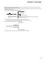
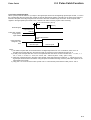
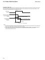
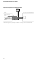
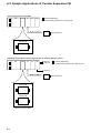
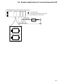
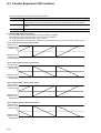
series
USER’S MANUAL
Digital High-Speed Input Module
FEH211a
Preface
This User’s Manual describes the system configuration, specifications and operations of MICREX-SX Series SPH Digital
High-Speed Input Module (NP1X3206-A). Read this manual thoroughly and use this product correctly.
Also read the related manuals listed below.
Title
Manual No.
Contents
User's Manual Instructions,
MICREX-SX Series
FEH200
Describes the MICREX-SX Series memory, language,
system definitions, etc.
User's Manual Hardware,
MICREX-SX Series SPH
FEH201
Describes the MICREX-SX Series system configuration and
hardware specifications and handling of modules.
User's Manual Digital High-Speed Output
Module, MICREX-SX Series SPH
FEH212
Describes the specifications and operations of MICREX-SX
Series Pulse Output Module used for simplified positioning.
User's Manual D300winV2 <Reference>,
MICREX-SX Series
FEH254
Describes the menus, icons and detailed operations of
D300winV2.
User's Manual D300winV3 <Reference>,
MICREX-SX Series
FEH257
Describes the menus, icons and detailed operations of
D300winV3.
In addition to the above manuals, the following Fuji Electric FA Components & Systems Co., Ltd. site offers various
manuals and technical documents associated with MICREX-SX.
URL http://www.fujielectric.co.jp/fcs/eng/
Notes
1. This manual may not be transcribed or reproduced in whole or part without permission.
2. The contents of this manual including the specifications are subject to change without prior notice.
3. This manual has been prepared with extreme care; however, if you find any ambiguous or incorrect description in
this manual, please contact us at one of the addresses listed at the end of this manual. At this time, inform us of
the manual No. given on the cover page.
Safety Precautions
Thoroughly read “Safety Precautions” before using this product.
In this manual, safety precautions are classified into “Warning” and “Caution” levels.
Warning : Incorrect handling of the device may result in death or serious injury.
Caution
: Incorrect handling of the device may result in minor injury and/or property damage.
Some items indicated as
Caution may also result in a serious accident.
Because the safety instructions in any level give important information, be sure to strictly observe them. Specially
important items are given below; they are also indicated in the manual text along with the symbols above.
Warning
◊ While the power is supplied, do not touch energized parts such as terminals, or electric shock may occur.
◊ Before performing mounting, demounting, wiring, maintenance or inspection, be sure to set the power OFF, or electric
shock, malfunction or fault may occur.
◊ Configure the emergency stop circuit, interlock circuit, etc. outside the PLC; otherwise, fault in PLC may cause damage
to the machine or accident.
◊ Do not connect in wrong directions, charge, disassemble, deform, throw in fire, or short-circuit the batteries. Doing so
may cause bursting or fire.
◊ Do not use batteries with deformation, leakage or other abnormalities, or bursting or fire may occur.
◊ Never open the FG terminal with LG-FG short-circuited, or electric shock may occur. (Be sure to ground that terminal.)
Safety Precautions
Caution
◊ If damage or deformation is found on the product when unpacking, do not use it, or fault or malfunction may occur.
◊ Do not give a shock to the product by dropping or falling it, or damage to the product or malfunction may occur.
◊ Install the product based on the instructions given in the instructions and other manuals. Inappropriate installation may
cause the product to fall, malfunction or become faulty.
◊ Use the product under the rated voltage and current specified in the instructions and other manuals. Using the product
under conditions outside the ratings may cause fire, malfunction or fault.
◊ Use (store) the product under the environmental conditions specified in the instructions and other manuals. Using
(storing) the product under high temperature or humidity or in environment containing dust, corrosive gas, oil, organic
solvent, vibrations with specially large amplitude, or shock may cause electric shock, fire, malfunction or fault when the
product is used.
◊ Select electric cables suitable for voltages and currents applied and secure them with the specified torque.
Inappropriate wiring or securing may cause fire, product falling, malfunction, or fault.
◊ When making application, take care not to put dust, cable fragments or iron powder into the device, or fire, accident,
malfunction or fault may occur.
◊ After wiring has completed, be sure to remove dust cover paper from modules and units before starting operation.
Operating the product with dust cover paper placed will cause fire, accident, malfunction or fault.
◊ Be sure to ground the ground terminals, or electric shock, malfunction or fault may occur.
◊ Periodically check that terminal and set screws are securely tightened. Using the product with these screws loosened
may cause fire or malfunction.
◊ Be sure to place the attached connector cover on a connector unused, or malfunction or fault may occur.
◊ When performing program change or forced output during operation or starting or stopping operation, make sure of
safety. Operation errors may cause damages to the machine or accidents.
◊ Insert the loader connector in the correct direction, or fault or malfunction may occur.
◊ Before touching the PLC, discharge static electricity charged on your body by touching grounded metal parts, etc.
Excessive static electricity may cause malfunction or fault.
◊ Perform wiring correctly based on the instructions or other manuals. Wrong wiring may cause fire, accident or fault.
◊ When disconnecting the plug from a convenience outlet, do not hold the cord. Cut cables may cause malfunction or
fault.
◊ Do not perform system change (I/O module mounting or dismounting) with the power supplied. Doing so may cause
malfunction or fault.
◊ Never try to repair this product in the field. When necessary, request us for repair. Battery changes must be performed
taking care of connector connections, etc., or fire, accident or fault may occur.
◊ When cleaning the product, set the power OFF and use towel moistened with warm water. Use of thinner or other
organic solvent causes the device surface to be swollen or discolored.
◊ Do not remodel or disassemble this product, or fault may occur.
◊ When discarding this product, handle it as industrial waste.
◊ The product described in this manual has not been designed for the purpose of being used for devices or systems
involved with human lives.
◊ When you are studying about using the product described in this manual for nuclear control, aerospace field, medical
services, transportation equipment or passenger mobile bodies or for specific applications for such systems, please
contact one of our sales offices.
◊ When applying the product described in this manual to such facilities that are assumed to be involved with human lives
or cause occurrence of serious loss by faults of the product, be sure to install safety devices.
◊ The external power supply (24 VDC, etc.) connected to DC I/O terminals must be in the state of reinforced insulation
from AC power supply, or accident or fault may occur. (Use of power supply compliant with EN60950 is recommended.)
Revisions
* Manual No. is shown on the cover.
Printed on
* Manual No.
Revision contents
Mar. 2004
FEH211
First edition printed.
Aug. 2007
FEH211a
Clause 5-2-2, wiring diagram revised.
Contents
Preface
Safety Precautions
Revision
Contents
Page
Section 1 Overview .......................................................................................1-1
Section 2 Specifications ...............................................................................2-1
2-1 General Specifications .................................................................................................................. 2-1
2-2 Input Specifications ....................................................................................................................... 2-2
2-3 Pulse Catch Function ..................................................................................................................... 2-3
2-3-1 Pulse catch operation ............................................................................................................................ 2-3
2-3-2 Pulse catch reset ................................................................................................................................... 2-4
2-4 Names and Functions of Parts ..................................................................................................... 2-5
2-4-1 Names of parts ...................................................................................................................................... 2-5
2-4-2 Functions of parts .................................................................................................................................. 2-5
2-5 Outside Dimensions ....................................................................................................................... 2-7
Section 3 System Configuration ..................................................................3-1
3-1 Mounting to Base Board ................................................................................................................ 3-1
3-1-1 Mounting locations ................................................................................................................................ 3-1
3-1-2 Number of modules mounted ................................................................................................................ 3-1
Section 4 Software Interface ........................................................................4-1
4-1 Memory Assignments .................................................................................................................... 4-1
Section 5 Wiring ............................................................................................5-1
5-1 Precautions for Wiring Work ......................................................................................................... 5-1
5-2 External Connections .................................................................................................................... 5-2
5-2-1 External input signal interface ............................................................................................................... 5-3
5-2-2 Sample connection of high-speed input module ................................................................................... 5-4
Section 6 High-Speed Input Counter Expansion FB ..................................6-1
6-1 Overview of Counter Expansion FB ............................................................................................. 6-1
6-2 Sample Applications of Counter Expansion FB ......................................................................... 6-2
6-3 Counter Expansion FB Functions ................................................................................................ 6-4
6-3-1 Ring operation count range ................................................................................................................... 6-4
6-3-2 Count operation mode ........................................................................................................................... 6-5
6-4 Details of Counter Expansion FB ................................................................................................. 6-6
6-5 Memory Size of High-Speed Input Counter Expansion FB ...................................................... 6-10
6-6 Settings for Ring and Gate Operations ...................................................................................... 6-10
Section 1 Overview
Section 1 Overview
Digital High-Speed Input Module NP1X3206-A is mounted on the MICREX-SX Series base board (connected to the SX
bus) for 32-point input or 32-point pulse catch input.
The digital high-speed input module has a pulse counter input function, allowing to select up to four channels (two phases)
of input signals of up to 20 kHz.
1) Image of fetching signal with pulse catch function
NP1X3206-A
Port input
Input signal
Pulse catch input
The pulse catch function can
fetch signals of a minimum of
20 µs.
* One input signal is fetched simultaneously into the port input and
pulse catch input registers.
Note: Eight points of ports 1 to 8 can fetch pulse signals of a minimum of 20 µs.
Twenty-four points of ports 9 to 32 can fetch pulse signals of a minimum of 100 µs.
2) Image of fetching signal with pulse counter function
NP1X3206-A
Pulse counter input
8 points (two phases)
Note: When the pulse counter input function is used, the soft filter is unavailable.
1-1
Section 2 Specifications
Page
2-1 General Specifications ............................................................................................... 2-1
2-2 Input Specifications .................................................................................................... 2-2
2-3 Pulse Catch Function ................................................................................................. 2-3
2-3-1 Pulse catch operation ........................................................................................................... 2-3
2-3-2 Pulse catch reset .................................................................................................................. 2-4
2-4 Names and Functions of Parts .................................................................................. 2-5
2-4-1 Names of parts ...................................................................................................................... 2-5
2-4-2 Functions of parts ................................................................................................................. 2-5
2-5 Outside Dimensions ................................................................................................... 2-7
General Specifications
Section 2 Specifications
2-1 General Specifications
Items
Physical environment
conditions
Mechanical operating
conditions
Electrical operating
conditions
Specifications
Operating ambient
temperature
0 to 55° C
Storage temperature
-25 to +70° C
Relative humidity
20 to 95% (No condensation allowed.)
Degree of pollution
2
Anticorrosiveness
No corrosive gas allowed.
Possible altitud
Altitude 2000 m or less (Atmospheric pressure during transportation
70 kPa or more)
Vibration resistance
Single amplitude: 0.15 mm, Constant acceleration: 19.6 m/s2
Shock resistance
Peak acceleration: 147 m/s2
Noise immunity
Noise simulation method, risetime 1 ns, pulse width 1 µs, 1.5 kV
Electrostatic discharge
resistance
Contact discharging method: ±6 kV, Aerial discharging method: ±8
Radiation field resistance
10 V/m (80 MHz to 1000 MHz)
Structure
Incorporated in board, IP30
Cooling type
Natural cooling
Insulation type
Photocoupler insulation
Dielectric strength
1500 VAC for one minute between all external terminals and ground
terminal
Insulation resistance
10MΩ or more between all external terminals and ground terminal,
measured with 500 VDC insulation resistance tester
Internal power consumption
24 VDC, 50 mA or less (with all points ON)
Mass
Approximately 130 g
Outside dimensions
See Section 2-5.
2-1
2-2 Input Specifications
Items
Specifications
Number of input points
Input signal
conditions
Input circuit
characteristic
32 points (32 points/common circuit)
Rated voltage
24 VDC
Maximum allowable voltage
30 VDC
Allowable ripple ratio
5% or less
Input type
Source input
Rated current
4 mA (for 24 VDC)
Input impedance
5.6 kΩ
Standard operation OFF → ON 15 to 30 V
range
ON → OFF 0 to 5 V
Input delay time
OFF → ON Changeable at a time by parameter setting, (OFF → ON) – (ON → OFF)
0.1 – 0.1 ms, 1 – 1 ms, 3 – 3 ms, 3 – 10 ms, 10 – 10 ms, 30 – 30 ms,
ON → OFF 100 – 100 ms, no soft filter (See Note.)
Input type
Pulse catch function for 32 points,
Minimum pulse width 20 µs for ports 1 to 8, 100 µs for ports 9 to 32
Other functions
Connection
DC type 1
External connectio
One 40-pole connector (FCN- 365P040-AU)
Applicable electric cable size
AWG #23 or less (When soldered connector used)
Input signal display
Display selected for each of 16 points by switch
Green LED lit for each point ON, Logical side
ONL: Lit when normal (green LED), ERR: Abnormal (red LED)
Derating conditions
Ratio of simultaneous ON: Maximum 100% (for 26.4 VDC, 55° C)
Ratio of simultaneous ON: Maximum 75% (for 30 VDC, 55° C)
Number of occupied words
14 words (Input: 9 words, Output: 5 words)
Number of occupied slots
1 slot
Note: When the pulse counter input function is used, the soft filter is unavailable.
2-2
Pulse Catch
2-3 Pulse Catch Function
2-3-1 Pulse catch operation
When a pulse (minimum width 20 µs) is input to the signal input terminal of the digital high-speed input module, “1” is set in
the corresponding bit in the pulse catch register of the high-speed input module. Information of the pulse catch register is
fetched to the pulse catch flag assigned to the I/O area in the CPU module through the SX bus. Once the pulse catch
register in the high-speed input module is set, it remains set until it is reset by a pulse catch reset flag.
20 µs or more Notes 1) and 4)
Note 3)
External signal
Input filter time
Note 2)
Pulse catch register
in high-speed
input module
SX bus transmission
delay
Pulse catch flag
assigned to I/O
area
One tact cycle
One tact cycle
Notes:
1) The width of a pulse that can be fetched is the set digital input filter time +20 µs. Therefore, when “none” is
specified as the input filter time, the minimum width of a pulse that can be fetched becomes 20 µs.
2) A delay of the set input filter time occurs. The input filter time that can be set in this module is 0.1 – 0.1 ms, 1 – 1
ms, 3 – 3 ms, 3 – 10 ms, 10 – 10 ms, 30 – 30 ms, 100 – 100 ms for (OFF → ON) – (ON → OFF).
3) When the corresponding bit in the pulse catch register of the high-speed input module is “1,” a pulse input to the
signal input terminal cannot be fetched. Using the pulse catch data reset flag, reset the pulse catch register in the
high-speed input module.
4) Only ports 1 to 8 can be used to fetch a pulse of 20 µs. The minimum pulse width for other ports is 100 µs.
2-3
Pulse Catch
2-3 Pulse Catch Function
2-3-2 Pulse catch reset
After fetching a pulse catch signal with an application program, reset the pulse catch information. By setting ON the pulse
catch data reset flag assigned to the I/O area (Q area), the pulse catch register in the high-speed input module is reset
and the pulse catch flag assigned to the I/O area goes OFF.
Note 1)
Pulse catch
reset flag
Pulse catch register
in high-speed input
module
Pulse catch flag
assigned to
I/O area
SX bus transmission delay 1)
SX bus transmission delay 2)
Note 2)
1) + 2) ≤ 1- to 2-tact time
Notes:
1) The pulse catch register is reset at the rising edge of the pulse catch data reset flag. Therefore, when resetting the
pulse catch register again, the reset flag must be once set OFF.
2) After issuing a pulse catch data reset command from an application program, it takes 1- to 2-tact time before the
pulse catch flag assigned to the I/O area goes OFF (when the task can be executed at every scan in
synchronization with the tact time).
2-4
2-4 Names and Functions of Parts
2-4-1 Names of parts
1) Status display LEDs
ONL
0 1 2 3 4 5 6 7
ERR
8 9 10 11 12 13 14 15
0
2) LED display selection switch
1
3) Input connector slot
4) Specification name plate
0/1
2-4-2 Functions of parts
1) Status display LEDs
Indicate the states of NP1X3206-A operation and input signals.
ONL 0 1 2 3 4
5
6 7
ERR 8 9 10 11 12 13 14 15
Symbols
LED colors ON conditions
ONL
Green
Remains ON during normal operation
ERR
Red
Goes ON when this module or SX bus has an error.
0 to 15
Green
Goes ON when the input signal is ON.
Note: When the ON-period of the input signal is very short,
it may be invisible to the naked eye.
2) LED display selection switch
Used to select the address of the input signal to be displayed.
0
1
When the switch is on the left side, input signals to the first 16 points (%IX .1.0 to %IX .1.15) are
displayed.
When the switch is on the right side, input signals to the last 16 points (%IX .2.0 to %IX .2.15) are
displayed.
2-5
2-4 Names and Functions of Parts
3) Input connector slot
<Signal assignments>
B20
B1
A20
A1
CH1 for pulse
counter function
CH2 for pulse
counter function
Port 9
B20
A20
Port 21
Port 10
B19
A19
Port 22
Port 11
B18
A18
Port 23
Port 12
B17
A17
Port 24
Port 13
B16
A16
Port 25
Port 14
B15
A15
Port 26
Port 15
B14
A14
Port 27
Port 16
B13
A13
Port 28
Port 17
B12
A12
Port 29
Port 18
B11
A11
Port 30
Port 19
B10
A10
Port 31
Port 20
B9
A9
Port 32
C0
B8
A8
C0
C0
B7
A7
C0
Port 1
B6
A6
Port 5
C0
B5
A5
C0
Port 2
B4
A4
Port 6
Port 3
B3
A3
Port 7
C0
B2
A2
C0
Port 4
B1
A1
Port 8
CH3 for pulse
counter function
CH4 for pulse
counter function
Note: C0 is internally connected.
4) Specification name plate
The name plate placed on the right side of the module shows the manufacture date and serial number.
2-6
2-5 Outside Dimensions
35
(45.2)
90
1
105
0
(75)
2-7
Section 3 System Configuration
Page
3-1 Mounting to Base Board ............................................................................................ 3-1
3-1-1 Mounting locations ................................................................................................................ 3-1
3-1-2 Number of modules mounted ................................................................................................ 3-1
Section 3 System Configuration
3-1 Mounting to Base Board
3-1-1 Mounting locations
The digital high-speed input module is an input module connected to the SPH SX bus. The mounting locations on the base
board are as shown below.
Any locations except the power module mounting slots (two slots at the base board left end) are available.
<Base board without 6-slot base board>
Available slots
<6-slot base board>
Available slots
T-link interface
Note: Base boards of substations such as T-link or JPCN-1 are unavailable.
I/O
Power
supply
I/O
CPU
I/O
I/O
Power
supply
T-link master
Unavailable
3-1-2 Number of modules mounted
A maximum of 238 modules can be connected to the SX bus and a maximum of 254 modules can be connected in one
configuration including the links of the I/O master (restriction by hardware).
Note that the number of modules that can be connected is limited according to the number of words in the I/O areas (I and
Q areas) occupied by these modules.
512 words
14 words
36.5 ⇒ 36 modules
3-1
Section 4 Software Interface
Page
4-1 Memory Assignments ................................................................................................. 4-1
(1) Input signal registers (offset addresses +1, +2) ...................................................................................... 4-2
(2) Pulse catch flags (offset addresses +3, +4) ............................................................................................ 4-2
(3) Pulse catch data reset flags (offset addresses +10, +11) ....................................................................... 4-2
(4) Pulse catch enable edge set registers (offset addresses +12, +13) ....................................................... 4-3
(5) Pulse count register (Offset address +0) ................................................................................................ 4-4
(6) Pulse count data registers (Offset addresses +5, +6, +7, +8) ................................................................ 4-6
(7) Pulse count register (Offset address +9) ................................................................................................ 4-6
Section 4 Software Interface
4-1 Memory Assignments
The digital high-speed input module occupies an I/O area of 14 words (9 input words and 5 output words).
b15
b0
Offset
address +0
Pulse count register
+1
Input register 1
+2
Input register 2
+3
Pulse catch register 1
+4
Pulse catch register 2
+5
Pulse count data register 1
+6
Pulse count data register 2
+7
Pulse count data register 3
+8
Pulse count data register 4
+9
Pulse count register
+10
Pulse catch register 1
+11
Pulse catch register 2
+12
Pulse catch enable edge set register 1
+13
Pulse catch enable edge set register 2
High-speed input module →
CPU (9 words)
CPU →
high-speed input module (5 words)
4-1
4-1 Memory Assignments
(1) Input signal registers (offset addresses +1, +2)
Store the ON/OFF states of the signal input to the input signal pin (1: ON, 0: OFF).
Offset
address
+1
+2
15
14
13
12
11
10
9
8
7
6
5
4
3
2
1
0
Port 16 Port 15 Port 14 Port 13 Port 12 Port 11 Port 10 Port 9 Port 8 Port 7 Port 6 Port 5 Port 4 Port 3 Port 2 Port 1
B13
B14
B15
B16
B17
B18
B19
B20
A1
A3
A4
A6
B1
B3
B4
B6
Port 32 Port 31 Port 30 Port 29 Port 28 Port 27 Port 26 Port 25 Port 24 Port 23 Port 22 Port 21 Port 20 Port 19 Port 18 Port 17
A10
A11
A12
A13
A14
A15
A16
A17
A18
A19
A20
B9
B10
B11
B12
A9
Connector pin Nos.
For example, the ON/OFF information of the signal input to port 8 (connector No. A1) is stored in the 7th bit at offset
address +1. When the module SX bus station No. is “1,” the input signal address for port 8 in the application program
becomes “%IX1.1.7.”
(2) Pulse catch flags (offset addresses +3, +4)
At the rising or falling edge of the signal input to the input signal pin, “1” is set in the corresponding bit. The set pulse catch
information is reset by the pulse catch data reset flag.
Offset
address
+3
+4
15
14
13
12
11
10
9
8
7
6
5
4
3
2
1
0
Port 16 Port 15 Port 14 Port 13 Port 12 Port 11 Port 10 Port 9 Port 8 Port 7 Port 6 Port 5 Port 4 Port 3 Port 2 Port 1
B13
B14
B15
B16
B17
B18
B19
B20
A1
A3
A4
A6
B1
B3
B4
B6
Port 32 Port 31 Port 30 Port 29 Port 28 Port 27 Port 26 Port 25 Port 24 Port 23 Port 22 Port 21 Port 20 Port 19 Port 18 Port 17
A10
A11
A12
A13
A14
A15
A16
A17
A18
A19
A20
B9
B10
B11
B12
A9
Connector pin Nos.
For example, the pulse catch data of the signal input to port 8 (connector No. A1) is stored in the 7th bit at offset address
+3. When the module SX bus station number is “1,” the input signal address for port 8 in the application program becomes
“%IX1.3.7.”
(3) Pulse catch data reset flags (offset addresses +10, +11)
Reset the data set in the pulse catch register. At the rising edge of the corresponding bit in this register, the pulse catch
data corresponding to that bit is reset.
Offset
address
15
14
13
12
11
10
9
8
7
6
5
4
3
2
1
0
Port 16 Port 15 Port 14 Port 13 Port 12 Port 11 Port 10 Port 9 Port 8 Port 7 Port 6 Port 5 Port 4 Port 3 Port 2 Port 1
+10
B13
B14
B15
B16
B17
B18
B19
B20
A1
A3
A4
A6
B1
B3
B4
B6
Port 32 Port 31 Port 30 Port 29 Port 28 Port 27 Port 26 Port 25 Port 24 Port 23 Port 22 Port 21 Port 20 Port 19 Port 18 Port 17
+11
A10
A11
A12
A13
A14
A15
A16
A17
A18
A19
A20
B9
B10
B11
B12
A9
Connector pin Nos.
For example, when resetting the pulse catch data of the signal input to port 8 (connector No. A1), the 7th bit at offset
address +10 is set ON. When the module SX bus station No. is “1,” “%QX1.10.7” is set ON.
Note: The pulse catch data is reset at the rising edge of this flag.
4-2
4-1 Memory Assignments
(4) Pulse catch enable edge set registers (offset addresses +12, +13)
These registers are used to set the rising edge or falling edge of the input signal as the pulse catch timing.
1: Rising edge, 0: Falling edge
Offset
address
15
14
13
12
11
10
9
8
7
6
5
4
3
2
1
0
Port 16 Port 15 Port 14 Port 13 Port 12 Port 11 Port 10 Port 9 Port 8 Port 7 Port 6 Port 5 Port 4 Port 3 Port 2 Port 1
B13
B14
B15
B16
B17
B18
B19
B20
A1
A3
A4
A6
B1
B3
B4
B6
Port 32 Port 31 Port 30 Port 29 Port 28 Port 27 Port 26 Port 25 Port 24 Port 23 Port 22 Port 21 Port 20 Port 19 Port 18 Port 17
+13
A10
A11
A12
A13
A14
A15
A16
A17
A18
A19
A20
B9
B10
B11
B12
A9
+12
Connector pin Nos.
Notes
1) Precautions for using pulse catch input (applicable to versions before 20)
• When the power is set ON, activating the system or writing to the pulse catch enable edge set register, the pulse
catch data goes ON. Therefore, clear the pulse catch data before using it.
• Sample program 1 (Clearing pulse catch data until the timing that requires pulse catch)
(SX but station No.)
Pulse enable input
%QX
.10.0 (Pulse catch data reset)
%QX
.10.1 (Pulse catch data reset)
• Sample program 2 (Clearing pulse catch data at activation)
ON only in the first scan
(SX but station No.)
%QX
.10.0 (Pulse catch data reset)
%QX
.10.1 (Pulse catch data reset)
Normally, use pulse catch enable edge set register 1.
The pulse can be fetched at the edge of the input given.
• Sample program 3 (Fetching pulse at input ON-edge)
(SX but station No.)
MOV
DWORD#16#FFFFFFFF
%QD
.12 (Pulse catch enable edge set register)
When fetching a pulse at input OFF-edge, data of the corresponding pulse catch enable edge set register should
be “0.”
• 0: Falling edge (default)
4-3
4-1 Memory Assignments
(5) Pulse count register (Offset address +0)
• This register shows the status indication information signal when the high-speed input module is performing pulse
count operation.
8
Current value clear completion
Count operation status
Unused
Rotation direction
Current value clear completion
Count operation status
Signal name
7
6
5
4
3
2
1
0
Count operation status
9
Current value clear completion
10
Rotation direction
11
Unused
12
Count operation status
13
Current value clear completion
14
CH0
Rotation direction
15
Rotation direction
Address No.
CH1
Unused
CH2
CH3
Unused
CH No.
Description of signals
1) Signal name: Count operation status signal
Description
• Response signal for count enable command signal
0: Disabled, 1: Enabled
Input mode set signal
(PLC → PI)
“01”: Positive rotation pulse + Reverse rotation pulse
Count enable command signal
(PLC → PI)
“1”
A
A
Pulse count data register
(PLC ← PI)
In counting
A
Count operation status signal
(PLC ← PI)
Rotation direction signal
(PLC ← PI)
Count retained
A
“1”
“0”: In positive rotation
A: 1 to 2 tacts (The tact time varies depending on the program size
and tact time setting.)
4-4
4-1 Memory Assignments
2) Signal name: Current value clear completion signal
Description
• Response signal for current value clear command signal
1: Current value clear completion
Input mode set signal
“10”: Pulse command + Sign signal
(PLC → PI)
Count enable command signal
(PLC → PI)
“1”
A
A
Pulse count data register
(PLC ← PI)
“0”
A
A
Count operation status signal
(PLC ← PI)
“1”
Current value clear command signal
(PLC → PI)
“1”
A
Current value clear completion signal
(PLC ← PI)
“1”
Rotation direction signal
(PLC ← PI)
“0”: In positive rotation
A: 1 to 2 tacts (The tact time varies depending on the program size
and tact time setting.)
3) Signal name: Rotation direction signal
Description
• Indicates the status of the signal input to the high-speed input module.
“0”: In positive rotation, “1”: In negative rotation
Input mode set signal
“00”: 90° phase difference pulse
(PLC → PI)
Count enable command signal
(PLC → PI)
“1”
A
Pulse count data register
(PLC ← PI)
Counting
A
Count operation status signal
(PLC ← PI)
Rotation direction signal
(PLC ← PI)
“1”
“0”: In positive rotation
“1”: In reverse rotation
A: 1 to 2 tacts (The tact time varies depending on the program size
and tact time setting.)
4-5
4-1 Memory Assignments
(6) Pulse count data registers (Offset addresses +5, +6, +7, +8)
• These registers perform counting during counter input function operation by the high-speed input module.
Address No.
15
0
5
Pulse count data register (current value at channel 0)
6
Pulse count data register (current value at channel 1)
7
Pulse count data register (current value at channel 2)
8
Pulse count data register (current value at channel 3)
• The data type is UINT.
• When the maximum value is exceeded during pulse counting, the count becomes “0” and when the value is less than
“0,” it goes to the maximum value.
(7) Pulse count register (Offset address +9)
• This is a command signal for the high-speed input module.
7
6
5
4
3
2
Description of signals
1) Signal name: Count enable command signal
Description
• Count enable signal for the high-speed input module
“0”: Disabled, “1”: Enabled
Input mode set signal
“01”: Positive rotation pulse + Reverse rotation pulse
(PLC → PI)
Count enable command signal
(PLC → PI)
“1”
A
Pulse count data register
(PLC ← PI)
In counting
A
Count operation status signal
(PLC ← PI)
Rotation direction signal
(PLC ← PI)
“1”
“0”: In positive rotation
“1”: In reverse rotation
A: 1 to 2 tacts (The tact time varies depending on the program size
and tact time setting.)
• The response signal for the count enable signal is the count operation status signal.
• When the count enable signal is “1,” the external pulse signal is acceptable.
When the count enable signal is “0,” the external pulse signal is unacceptable.
4-6
1
0
Count enable command signal
8
Current value clear command signal
9
Input mode set signal
10
Count enable command signal
11
CH0
Current value clear command signal
12
Count enable command signal
Input mode set signal
Signal name
13
Current value clear command signal
14
CH1
Input mode set signal
15
Count enable command signal
Address No.
CH2
Input mode set signal
CH3
Current value clear command signal
CH No.
4-1 Memory Assignments
2) Signal name: Current value clear command signal
Description
• Clears the pulse count data register area of the high-speed input module to “0.”
1: Current value clear
Input mode set signal
“10”: Pulse command + Sign signal
(PLC → PI)
Count enable command signal
(PLC → PI)
“1”
A
A
Pulse count data register
(PLC ← PI)
“0”
A
A
Count operation status signal
(PLC ← PI)
“1”
Current value clear command signal
(PLC → PI)
“1”
A
Current value clear completion signal
(PLC ← PI)
Rotation direction signal
(PLC ← PI)
“1”
“0”: In positive rotation
A: 1 to 2 tacts (The tact time varies depending on the program size
and tact time setting.)
• The response signal for the current value clear command signal is the current value clear completion signal.
• The current value clear command signal can also be cleared during count operation.
3) Signal name: Input mode set signal
Description
• Set when performing counter operation by the high-speed input module.
3)-1 90° phase difference pulse
• Set address bits “2,” “3,” “6,” “7,” “10,” “11,” “14” and “15” to “0.” The input specifications are given below.
90° phase difference pulse (A-/B-phases, 4-multiply, maximum 80 kHz, duty 50%)
Positive
rotation
Negative
rotation
A-phase
t3
B-phase
t1
t1
t3
t2
Minimum pulse width: t1 > 20 µs, Minimum pulse cycle: t2 > 40 µs
Minimum edge interval: t3 > 20 µs
4-7
4-1 Memory Assignments
3)-2 Positive rotation pulse + Negative rotation pulse
• Set address bits “2,” “6,” “10” and “14” to “1.” The input specifications are given below.
Positive rotation pulse + Negative rotation pulse (maximum 20 kHz)
Positive
rotation
Negative
rotation
Positive rotation
pulse
Negative rotation
pulse
t1
t1
t3
t2
Minimum pulse width: t1 > 20 µs, Minimum pulse cycle: t2 > 40 µs
Minimum edge interval: t3 > 40 µs
3)-3 Pulse command + Sign signal
• Set address bits “3,” “7,” “11” and “15” to “1.” The input specifications are given below.
Pulse command + Sign signal (maximum 20 kHz)
Positive
rotation
Negative
rotation
Pulse command
Sign command
t1
t1
t2
t3
t4
Minimum pulse width: t1 > 20 µs, Minimum pulse cycle: t2 > 40 µs
Minimum edge interval: t3 > 20 µs before sign switching, t4 > 20 µs after sign switching
4-8
Section 5 Wiring
5-1 Precautions for Wiring Work ..................................................................................... 5-1
5-2 External Connections ................................................................................................. 5-2
5-2-1 External input signal interface ............................................................................................... 5-3
5-2-2 Sample connection of high-speed input module ................................................................... 5-4
Section 5 Wiring
5-1 Precautions for Wiring Work
1) Do not remove dust cover paper before wiring work completes.
When the wiring work has completed, be sure to remove dust cover paper before starting operation.
2) Separate high-voltage and power lines from the module input signal lines and do not place these lines in parallel.
3) Use appropriate electric cables for wiring.
Available connector and cable size are listed below.
4) When using the high-speed input module as a counter, use common sealed cables.
<Available connector and cable size>
Use the 40-pin connector given below manufactured by Fujitsu.
Type
Model (Manufactured by Fujitsu)
Cable size
Soldered
Socket
FCN-361J040-AU
AWG23 or less
(0.26 mm2 or less)
Connector cover
FCN-360C040-B
Soldered type (Note)
Note: As a soldered type connector, NP8V-CN (manufactured by Fuji Electric) is available.
5-1
5-2 External Connections
Signal names
Connector pin Nos.
B20
B1
A20
A1
·
·
·
·
·
·
·
·
·
·
·
+
Port 9
B20 A20
Port 21
Port 10
B19 A19
Port 22
Port 11
B18 A18
Port 23
Port 12
B17 A17
Port 24
Port 13
B16 A16
Port 25
Port 14
B15 A15
Port 26
Port 15
B14 A14
Port 27
Port 16
B13 A13
Port 28
Port 17
B12 A12
Port 29
Port 18
B11 A11
Port 30
Port 19
B10 A10
Port 31
Port 20
B9
A9
Port 32
C0
B8
A8
C0
C0
B7
A7
C0
Port 1
B6
A6
Port 5
C0
B5
A5
C0
Port 2
B4
A4
Port 6
Port 3
B3
A3
Port 7
C0
B2
A2
C0
Port 4
B1
A1
Port 8
Note: Common pin C0 is internally and electrically connected.
5-2
·
·
·
·
·
·
·
·
·
·
·
5-2 External Connections
5-2-1 External input signal interface
Signal name
Circuit drawing
High-speed input ports 1 to 8
1.5 kΩ
5.6 kΩ
Port 1
1.5 kΩ
5.6 kΩ
Port 2
1.5 kΩ
5.6 kΩ
Port 8
C0
High-speed input ports 9 to 32
1 kΩ
5.6 kΩ
Port 9
1 kΩ
5.6 kΩ
Port 10
1 kΩ
5.6 kΩ
Port 32
C0
5-3
5-2 External Connections
5-2-2 Sample connection of high-speed input module
Sample: Connecting OMRON encoder (Model: E6B2-CWZ6C)
External
power supply
(24 VDC)
Encoder
High-speed input module (NP1X3206-A)
Encoder power supply
(24 VDC)
A-phase pulse
B-phase pulse
Port 1 (B6)
C0
(B5)
Port 2 (B4)
Note: When using the high-speed input module as a counter input, use common sealed cables.
5-4
Section 6 High-Speed Input Counter Expansion FB
Page
6-1 Overview of Counter Expansion FB .......................................................................... 6-1
6-2 Sample Applications of Counter Expansion FB ...................................................... 6-2
(1) Counting pulses from outside ................................................................................................................. 6-2
(2) Making output when a certain angle (pulses) is attained (Varicam control) ............................................ 6-2
(3) Simplified position control (to know work location) ................................................................................. 6-3
6-3 Counter Expansion FB Functions ............................................................................. 6-4
6-3-1 Ring operation count range ................................................................................................... 6-4
(1) For 16-bit positive rotation specification ................................................................................................. 6-4
(2) For 16-bit negative rotation specification ................................................................................................ 6-4
(3) For 32-bit positive rotation specification ................................................................................................. 6-4
(4) For 32-bit negative rotation specification ................................................................................................ 6-4
6-3-2 Count operation mode .......................................................................................................... 6-5
(1) Ring operation mode .............................................................................................................................. 6-5
(2) Gate operation mode .............................................................................................................................. 6-5
6-4 Details of Counter Expansion FB .............................................................................. 6-6
(1) Signal names for high-speed input expansion FB .................................................................................. 6-7
6-5 Memory Size of High-Speed Input Counter Expansion FB ................................... 6-10
6-6 Settings for Ring and Gate Operations ................................................................... 6-10
(1) Ring operation ....................................................................................................................................... 6-10
(2) Gate operation ...................................................................................................................................... 6-10
Section 6 High-Speed Input Counter Expansion FB
6-1 Overview of Counter Expansion FB
• The counter function can be achieved by using the high-speed input module (NP1X3206-A) together with the high-speed
input counter expansion FB.
• The counter expansion FB specifications are as follows:
(1) Pulse input mode selection
1) 90° phase difference pulse
2) Positive rotation pulse + Negative rotation pulse
3) Pulse command + Sign signal
(2) Operation mode
1) Ring operation
2) Gate operation
3) Reset operation
(3) Counting range
1) Signed binary 16 bits (–32768 to 32767)
2) Signed binary 32 bits (–2147483648 to 2147483647)
6-1
6-2 Sample Applications of Counter Expansion FB
(1) Counting pulses from outside
PS
CPU
PI
DI
DO
: SX bus folded plug
PI : Count fetching enabled up to 20 kHz (4ch)
Pulse generator
Counter FB
Memory in CPU module
(2) Making output when a certain angle (pulses) is attained (Varicam control)
PS
CPU
PI
DI
DO
Output 1
Output 2
: SX bus folded plug
PI : Count fetching enabled up to 20 kHz (4ch)
Output 3
Pulse generator
Counter FB
Varicam FB
Memory in CPU module
6-2
6-2 Sample Applications of Counter Expansion FB
(3) Simplified position control (to know work location)
PS
CPU
PI
PO
DO
: SX bus folded plug
PI : Count fetching enabled up to 20 kHz (4ch)
PO : Output enabled up to 20 kHz (4ch)
(Command)
Amplifier
M
(Feedback)
PG
Counter FB
Simplified positioning FB
Memory in CPU module
6-3
6-3 Counter Expansion FB Functions
• The counter expansion FB has the functions listed below.
Functions
Description
Ring operation
• Counting operation that leads to the minimum value when the maximum value is exceeded
during pulse counting and to the maximum value when the minimum value is not attained
Gate operatio
• Pulse counting operation performed only when the internal gate input is in counting enabled
state
Reset operation
• Count value reset by internal reset input
6-3-1 Ring operation count range
• The count value always changes without causing overflow or underflow.
The maximum value varies depending on the 16-/32-bit specification.
For 32-bit specification, the input count value is output.
For 16-bit specification, the high-order 16 bits are truncated from the input count value and the result is output.
(1) For 16-bit positive rotation specification
Positive 16-bit
maximum value
00007FFF(H)
0
Negative 16-bit
maximum value
FFFF8000(H)
(2) For 16-bit negative rotation specification
Positive 16-bit
maximum value
00007FFF(H)
0
Negative 16-bit
maximum value
FFFF8000(H)
(3) For 32-bit positive rotation specification
Positive 32-bit
maximum value
7FFFFFFF(H)
0
Negative 32-bit
maximum value
80000000(H)
(4) For 32-bit negative rotation specification
Positive 32-bit
maximum value
7FFFFFFF(H)
0
Negative 32-bit
maximum value
80000000(H)
6-4
6-3 Counter Expansion FB Functions
6-3-2 Count operation mode
(1) Ring operation mode
• Input pulse mode and 16-/32-bit count selection are set by the function block (FB). No overflow or underflow occurs.
Internal reset
Positive
rotation
Count pulse
Negative
rotation
Positive
maximum
value
Positive
Count value
Negative Count reset
to 0
Negative
maximum
value
* The counting range can be set to 16- or 32-bit signed binary value by internal setting.
(2) Gate operation mode
• Pulse counting is performed when the internal gate input is in count enabled state.
Internal gate: Counting enabled when the 4th bit of the bit command signal is ON. (Setting required for every four
channels.)
Internal reset
Pulse counting enabled
Pulse counting enabled
Internal gate
input
Positive
rotation
Count pulse
Negative
rotation
Positive
maximum
value
Positive
Count value
Negative Count reset
to 0
Negative
maximum
value
* Pulse counting is performed only when the internal gate input is in count enabled state.
When the gate input is in the count disabled state, no pulse counting occurs for pulse inputs, if any.
* The counting range can be set to 16- or 32-bit signed binary value by internal setting.
6-5
6-4 Details of Counter Expansion FB
• The counter expansion FB configuration and I/O signal list are given below.
_MHCNTD (High-speed input counter FB)
BOOL
Activation command
(START)
BOOL
BOOL
_MTBITC2
INT
_MTHC2IN
Initialization completion
(INI_END)
BOOL
Internal reset command
(RST_CMD)
Internal reset command response
(RST_OK)
BOOL
Internal gate command
(GATE_CMD)
Internal gate command response
(GATE_OK)
BOOL
Bit command signal 1
(BITCMD1)
Bit command signal 1 response
(STS_DAT)
CH specification
(CH_SEL)
_MTSTS2
Count value (CNT_DAT)
DINT
In counting (CNT_RUN)
BOOL
Rotation direction (DIR)
BOOL
Input variable (INDAT)
Input variable (INDAT)
_MTHC2IN
Note
Note
_MTHC2OT
Output variable (OUTDAT)
Output variable (OUTDAT)
_MTHC2OT
Note: Indicates the IN_OUT parameter.
List of high-speed input counter FB I/O signals
No.
Data names
Data type
I/O
Signal variable names
1
Activation command
BOOL
Input
START
2
Internal reset command
BOOL
Input
RST_CMD
3
Internal gate command
BOOL
Input
GATE_CMD
4
Bit command signal 1
_MTBITC2
Input
BITCMD1
5
CH specification
INT
Input
CH_SEL
6
Initialization completion
BOOL
Output
INI_END
7
Internal reset command response BOOL
Output
RST_OK
8
Internal gate command response
BOOL
Output
GATE_OK
9
Bit command signal 1 response
_MTSTS2
Output
STS_DAT
10
Count value
DINT
Output
CNT_DAT
11
In counting
BOOL
Output
CNT_RUN
12
Rotation direction
BOOL
Output
DIR
13
Input variable
_MTHC2IN
IN_OUT
INDAT
14
Output variable
_MTHC2OT IN_OUT
6-6
OUTDAT
Remarks
6-4 Details of Counter Expansion FB
(1) Signal names for high-speed input expansion FB
1) Activation command (START/BOOL)
“1”: Starts initialization processing (counter current value clear processing).
When initialization processing has completed, “initialization completion” goes ON.
At the activation command rising edge, the signal status of bit command signal 1 is reflected to the high-speed
input module.
2) Internal reset command (RST_CMD/BOOL)
“1”: For the high-speed input module, sets “current value clear command” ON.
3) Internal gate command (GATE_CMD/BOOL)
• Command signal to be used when gate operation mode is enabled by count operation mode.
“1”: For the high-speed input module, sets “count enable command” ON.
“0”: For the high-speed input module, sets “count enable command” OFF.
4) Bit command signal 1 (BITCMD1/_MTBITC2 type with elements of BOOL type)
• At the rising edge of the activation command, this is reflected to the high-speed input module.
a) Input pulse mode (PLS_U/PLS_L)
“0”/“0”: 90°¡ phase difference pulse
“0”/“1”: Positive rotation pulse + Negative rotation pulse
“1”/“0”: Sign signal + command pulse
“1”/“1”: Pulse counting inhibited
b) 16-/32-bit count selection (CNT_SEL)
“0”: 16-bit count selection
“1”: 32-bit count selection
Notes
• For the high-speed input module, only 16-bit count specification is enabled.
By using the expansion FB, 16- or 32-bit specification can be selected.
c) Gate operation mode selection enable (GATE_MOD)
“0”: Gate operation disabled (For high-speed input module, “count enable command signal” is always ON.
“1”: Gate operation enabled (Referencing the internal gate command, “count enable command signal” is set ON for the
high-speed input module.
5) CH specification (CH_SEL/INT)
• For expansion FB, CH specification is enabled only for “0,” “1,” “2” or “3.”
6) Internal reset command response (RST_OK/BOOL)
• Used as a response signal for internal reset command (RST_CMD).
7) Internal gate command response (GATE_OK/BOOL)
• Response signal for gate operation mode enable command.
6-7
6-4 Details of Counter Expansion FB
8) Bit command signal 1 response (STS_DAT/_MTSTS2 type with elements of BOOL type)
• Outputs operation mode of the high-speed input expansion FB after the rising edge of activation command (START).
a) Input pulse mode (PLS_U/PLS_L)
“0”/“0”: 90fl phase difference pulse
“0”/“1”: Positive rotation pulse + Negative rotation pulse
“1”/“0”: Sign signal + command pulse
“1”/“1”: Pulse counting inhibited
b) 16-/32-bit count selection (CNT_SEL)
“0”: 16-bit count selection
“1”: 32-bit count selection
c) Gate operation mode selection enable (GATE_MOD)
“0”: Gate operation disabled (For the high-speed input module, “count enable command signal” is always ON.
“1”: Gate operation enabled (Referencing the internal gate command, “count enable command signal” is set ON for the
high-speed input module.
9) Count value (CNT_DAT/DINT)
• Outputs the count value.
The output range varies depending on the 16-/32-bit count selection.
16-bit specification: 8000 to 7FFF, –32768 to 32767
32-bit specification: 80000000 to 7FFFFFFF, –2147483648 to 2147483647
10) In counting (CNT_RUN/BOOL)
• Outputs the high-speed input module counting status.
“0”: Disabled
“1”: Enabled
11) Rotation direction (DIR/BOOL)
• Indicates the status of the signal input to the high-speed input module.
“0”: In positive rotation
“1”: In negative rotation
12) Initialization completion (INI_END/BOOL)
• Initialization completion goes ON when the initialization processing has completed after the rising edge of activation
command (START).
13) Input variable (INDAT/_MTHC2IN type with array of WORD type)
• Elements are in the array of I/O area in I/O map.
The I/O areas are listed below.
6-8
Address No.
15
0
Pulse count register
1
Input register 1
2
Input register 2
3
Pulse catch register 1
4
Pulse catch register 2
5
Pulse count data register 1
6
Pulse count data register 2
7
Pulse count data register 3
8
Pulse count data register 4
0
6-4 Details of Counter Expansion FB
Supplementary explanation: Set the following in the program. (V000 is a tentative name.)
VAR
V000 AT %IW .0 : _MTHC2IN ;
END_VAR
Note:
denotes an SX station No.
14) Output variable (OUTDAT/_MTHC2OT type with array of WORD type)
• Elements are in the array of I/O area in I/O map.
Address No.
15
0
Pulse count register
1
Pulse catch register 1
2
Pulse catch register 2
3
Pulse catch enable edge set register 1
4
Pulse catch enable edge set register 2
0
Supplementary explanation: Set the following in the program. (V001 is a tentative name.)
VAR
V000 AT %QW .9 : _MTHC2OT ;
END_VAR
Note:
denotes an SX station No.
6-9
6-5 Memory Size of High-Speed Input Counter Expansion FB
FB name
FB mnemonic
Object CP
Positioning
module
User program
size
User FB
instance
Retention data
FB for highspeed input
_MHCNTD
NP1PSNP1PH-
NP1X3206-A
275
70
–
6-6 Settings for Ring and Gate Operations
Settings for ring and gate operations using the high-speed input counter expansion FB are given below.
(1) Ring operation
1) Set CH specification (CH_SEL) (INT type).
• The high-speed input module has counter functions for a maximum of four channels.
2) Set bit command signal 1 (BITCMD1).
• Set the input pulse mode.
• Set the 16- or 32-bit counter to be used.
(The high-speed input module is a 16-bit ring counter.)
3) Activation command (START)
• Performs initialization processing.
(2) Gate operation
1) Set CH specification (CH_SEL) (INT type).
• The high-speed input module has counter functions for a maximum of four channels.
2) Set bit command signal 1 (BITCMD1).
• Set the input pulse mode.
• Set the 16- or 32-bit counter to be used.
(The high-speed input module is a 16-bit ring counter.)
• Set gate operation enable (GATE_CMD).
3) Set internal gate command (GATE_CMD).
4) Activation command (START)
• Performs initialization processing.
6-10
Gate City Ohsaki, East Tower,
11-2, Osaki 1-chome, Shinagawa-ku, Tokyo 141-0032, Japan
E-mail: [email protected]
URL: http://www.fujielectric.com/
Materials covered in this document are subject to revision due to the modification of the product.
Issued as FE consolidated edition, June 2011