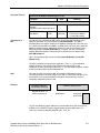
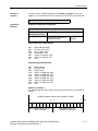
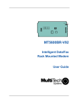
1
SIMATIC
Loadable Driver for CP 341
Modbus ASCII Slave with 32-Bit Extensions
Manual
Preface, Contents
SIMATIC
Loadable Driver for CP341
Modbus Protocol
ASCII Format
S7 is Slave
with 32-Bit Extensions
Manual
Product Description
1
Installation
2
Mode of Operation
3
Commissioning the Driver
4
Commissioning the FB
5
CPU – CP Interface
6
Transmission Protocol
7
Function Codes
8
Diagnostics of the Driver
9
Diagnostics of the FB
10
Appendices
Technical Data
A
Wiring Diagrams Multipoint
B
Access Cheat Sheat
C
Literature List
D
Glossary
Edition 1.0
Safety Precautions and
Warnings
This manual contains warnings, which you should note for your own safety as well as for the
prevention of damage to property. These warnings are indicated by means of a triangle and
displayed as follows in accordance with the level of danger:
_____________________________________________________________________
Danger
!
indicates that death, severe personal injury or substantial damage
will result if proper precautions are not taken.
_____________________________________________________________________
_____________________________________________________________________
Warning
!
indicates that death, severe personal injury or substantial damage can result if proper
precautions are not taken.
_____________________________________________________________________
_____________________________________________________________________
Caution
!
indicates that minor personal injury or property damage can result if proper precautions are not
taken.
_____________________________________________________________________
_____________________________________________________________________
Notice
draws your attention to particularly important information on the product, handling the product, or
to a particular part of the documentation.
_____________________________________________________________________
Qualified
Personnel
The equipment may be commissioned and put into operation by qualified personnel only. For
the purpose of safety relevant warnings of this manual a qualified person is one who is
authorized to commission, ground and tag devices, systems and circuits.
Correct Usage
Please note the following:
____________________________________________________________________________
!
Trademarks
Warning
This device and its components may only be used for the applications described in the catalog or
the technical description, and only in connection with devices or components from other
manufacturers which have been approved or recommended by Siemens.
This product can only function correctly and safely if it is transported, stored, set up, and
installed correctly, and operated and maintained as recommended.
®
®
SIMATIC and SINEC are registered trademarks of SIEMENS AG.
The other brand names in this manual may be trademarks use of which by third parties for their
purposes may infringe the proprietors’ rights.
Copyright © Siemens AG 2006 All Rights Reserved
Disclaimer of Liability
The reproduction, transmission, or use of this document or its contents is
not permitted without express written authority. Offenders will be liable
for damages. All rights reserved, including rights created by patent grant
or registration of a utility model or design, are reserved.
We have checked the contents of this manual for agreement with the
hardware and software described. Since deviations cannot be precluded
entirely, we cannot guarantee full agreement. However, the data in this
manual are reviewed regularly and any necessary corrections included
in subsequent editions. Suggestions for improvement are welcome.
© Siemens AG 2006
Subject to change without prior notice.
Preface
Preface
Purpose of this
Manual
The information in this manual will enable you to establish and commission a
data link between a CP 341 and a “Modbus capable” control system.
Required Basic
Knowledge
You require a general knowledge in the field of automation engineering to be
able to understand this manual.
In addition, you should know how to use computers or devices with similar
functions (e.g. programming devices) under Windows 95/98/2000/NT or XP
operating systems. Since loadable driver are based on the STEP 7 software,
you should also know how to operate it. This is provided in the manual
“Programming with STEP 7 V5.2”.
Contents of the
Manual
This manual describes the loadable driver functions and how to create a link to
the hardware and software of communication processor CP 341.
The manual contains the following subjects:
• Product Description / Installation
• Commissioning the Driver / Installation / Parameterization
• Interface CPU-CP
• Transmission Protocol
• Diagnostics Driver
• Application Example
Validity of the
Manual
This manual Issue is valid for the following software package:
Product
Identification No.
from Version
Loadable Driver for CP 341
Modbus ASCII Slave
6ES7870-1CA00-0YA0
1.0
Note
This manual contains the driver description as is valid at the time of publication.
How to access the
information in this
manual
To enable you to access the information in this manual more easily, we would
like to draw your attention to the following:
• The next few pages contain a complete list of contents.
Loadable Driver CP341: MODBUS ASCII Slave with 32-Bit Extensions
6ES7870-1CA00-0YA0; Manual Edition 1.0
iii
Preface
Further sources of
information
Any further information regarding CP 341 (installation, commissioning etc.) can
be found in the following manual:
SIEMENS
SIMATIC
CP341 Point to Point Communication
Installation and Parameter Assignment
Manual
C79000-G7076-C341-..
Further information regarding STEP7 can be found in the following manuals:
SIEMENS
SIMATIC Software
Standard Software for S7 and M7
STEP7 User Manual
C79000-G7000-C502-..
SIEMENS
SIMATIC Software
System Software for S7-300/400
System- and Standard Functions
Reference Manual
C79000-G7000-C503-..
Queries
Should you have any queries regarding the use of the driver described in this
manual, which are not answered in this documentation please contact the
relevant person at Siemens who supplied you with this driver.
Terminology
This documentation uses the terms CP or CP341.
Scope of
Application
The driver described in this manual serves as a loadable protocol for CP341,
which may be used instead of Standard Protocols 3964R, RK512, and ASCII.
Note
With this driver, modifications or expansions to the sequences between CP and
CPU are possible.
These modifications and expansions may apply in particular to event classes or
event numbers available for diagnostic purposes.
Furthermore please note that this manual only describes the modifications and
expansions as against the standard functions. Basic information may be found in
the manuals mentioned in section “Further Sources of Information”.
In order to ensure safe use of the driver, detailed knowledge of the functionality
of CP341 is a pre-requisite.
Loadable Driver CP341: MODBUS ASCII Slave with 32-Bit Extensions
6ES7870-1CA00-0YA0; Manual Edition 1.0
iv
Contents
Contents
1
2
3
4
Product Description.......................................................................................................... 1-1
1.1
Usage Possibilities............................................................................................... 1-1
1.2
Hardware and Software Prerequisites................................................................. 1-2
1.3
Summary of the Modbus Protocol ....................................................................... 1-3
1.4
Notes.................................................................................................................... 1-4
Installation ......................................................................................................................... 2-1
2.1
Use of the Dongle ................................................................................................ 2-1
2.2
Interface Connection............................................................................................ 2-1
Mode of Operation of the Data Link ................................................................................ 3-1
3.1
Components of the SIMATIC / Modbus Slave Data Link .................................... 3-1
3.2
Task Distribution .................................................................................................. 3-2
3.3
Used Modbus Function Codes ............................................................................ 3-2
3.4
Data Areas in the SIMATIC CPU......................................................................... 3-3
3.5
Access with Bit-Orientated Function Codes ........................................................ 3-4
3.6
Access with Register-Orientated Function Codes............................................... 3-5
3.6.1
Access to Registers “with 32-Bit Register” Not Set ............................................. 3-6
3.6.2
Access to Registers ”with 32-Bit Register” Set.................................................... 3-8
3.6.3
Access with Function Code 4 .............................................................................. 3-9
3.7
Enable Write Access.......................................................................................... 3-10
Commissioning the Driver ............................................................................................... 4-1
4.1
Installing the Driver on the STEP 7 Programming Device / PC........................... 4-1
4.2
Uninstalling the Driver.......................................................................................... 4-2
4.3
Configuring the Data Link CP in Step7................................................................ 4-2
4.4
Assigning Parameters to the CP ......................................................................... 4-3
4.5
Assigning Parameters to the Loadable Driver ..................................................... 4-4
4.6
Loading the Driver to the CP ............................................................................... 4-4
Loadable Driver CP341: MODBUS ASCII Slave with 32-Bit Extensions
6ES7870-1CA00-0YA0; Manual Edition 1.0
v
Contents
4.7
5
6
Loading the Configuration and Parameter Assignment Data .............................. 4-5
Modbus ASCII Driver Specific Parameters..................................................................... 5-1
5.1
Modbus Slave Protocol Parameters .................................................................... 5-1
5.2
Conversion of Modbus Addresses for Bit Functions ........................................... 5-3
5.3
Conversion of Modbus Addresses for Register Functions .................................. 5-7
5.3.1
Conversion for Register Functions in Standard Mode......................................... 5-7
5.3.2
Conversion for Register Functions in Mode “with 32-Bit Register”...................... 5-9
5.4
Limits for Write Functions .................................................................................. 5-10
5.5
RS422/485 (X27) Interface ................................................................................ 5-12
5.6
RS232 Secondary Signals................................................................................. 5-13
Commissioning the Communications FB....................................................................... 6-1
6.1
Installing the FB ................................................................................................... 6-1
6.2
STEP7 Project ..................................................................................................... 6-1
6.3
FB 81 Parameters................................................................................................ 6-3
6.4
Program Call........................................................................................................ 6-4
6.5
Cyclic Operation .................................................................................................. 6-6
7
CPU – CP Interface............................................................................................................ 7-1
8
Transmission Protocol ..................................................................................................... 8-1
9
8.1
Message Structure............................................................................................... 8-1
8.2
Exception Responses .......................................................................................... 8-5
8.3
RS 232C Secondary Signals ............................................................................... 8-6
Function Codes ................................................................................................................. 9-1
9.1
Function Code 01 – Read Coils........................................................................... 9-2
9.2
Function Code 02 – Read Discrete Inputs........................................................... 9-5
9.3
Function Code 03 – Read Holding Registers in Standard Mode......................... 9-8
9.4
Function Code 03 – Read Holding Registers in Mode “with 32-Bit Register” ... 9-11
9.5
Function Code 04 – Read Input Registers ........................................................ 9-16
9.6
Function Code 05 – Write Single Coil................................................................ 9-19
Loadable Driver CP341: MODBUS ASCII Slave with 32-Bit Extensions
6ES7870-1CA00-0YA0; Manual Edition 1.0
vi
Contents
10
11
9.7
Function Code 06 – Write Single Register in Standard Mode........................... 9-21
9.8
Function Code 06 – Write Single Register in Mode “with 32-Bit Register”........ 9-24
9.9
Function Code 08 - Diagnostics ....................................................................... 9-28
9.10
Function Code 15 – Write Multiple Coils ........................................................... 9-29
9.11
Function Code 16 – Write Multiple Registers in Standard Mode....................... 9-32
9.12
Function Code 16 – Write Multiple Registers in Mode “with 32-Bit Register” ... 9-35
Diagnostics of the Driver................................................................................................ 10-1
10.1
Diagnostics via Display Elements (LEDs) ......................................................... 10-2
10.2
Diagnostic Messages of the Function Blocks of the CP 341............................. 10-2
10.3
Table of Errors / Events ..................................................................................... 10-3
10.3.1
Error Codes for “CPU Job Errors” ..................................................................... 10-3
10.3.2
Error Codes for “Receive Errors”....................................................................... 10-4
10.3.3
Error Codes in SYSTAT for “General Processing Errors” ................................. 10-6
Diagnostics of the Communications FB....................................................................... 11-1
11.1
Diagnostics via Parameters ERROR_NR, ERROR_INFO................................ 11-1
11.1.1
Errors during “Initialization”................................................................................ 11-2
11.1.2
Errors during “Processing of Function Codes” .................................................. 11-2
11.1.3
“Other” Errors..................................................................................................... 11-3
A
Technical Data...................................................................................................................... 1
B
Wiring Diagrams Multipoint ................................................................................................ 1
C
Access Cheat Sheat............................................................................................................. 1
D
Literature List ....................................................................................................................... 1
Glossary .......................................................................................................................................... 1
Loadable Driver CP341: MODBUS ASCII Slave with 32-Bit Extensions
6ES7870-1CA00-0YA0; Manual Edition 1.0
vii
Product Description
1
Product Description
1.1
Usage Possibilities
Position in the
System
The Driver described here is a software product for communication processor
CP341.
Environment
CP341 can be used in automation systems S7-300 and can establish serial
communication links to partner systems.
Function of the
Driver
This driver, together with the appropriate function block, enables you to establish
a communication link between communication module CP341 and “Modbus
capable” control systems.
The transmission protocol used is the Modbus Protocol in ASCII Format. In
addition, de-facto standard 32-bit extensions are supported for accessing floating
point and double-word registers in compatible slaves. Data transmission is carried
out in accordance with the Master-Slave principle.
The Modbus master has the initiative during the transmission while the the
CP341 (installed in the the S7 CPU rack) operates as the slave.
Function Codes 01, 02, 03, 04, 05, 06, 08, 15 and 16 can be used for
communication between the CP and the host system.
The MODBUS “Starting Address” in the request message from the master is
interpreted by the driver “in an S7 way.”
This means that it is possible to:
•
•
read and write memory bits, outputs, data blocks,
read inputs bits
in the S7 CPU.
The interpretation of the MODBUS “Starting Address” is explained in the following
sections.
Usable Interfaces
and Protocols
You can use CP341 with RS232, TTY, or RS422/485 (X27) interfaces.
With this driver, it is possible to use the RS422/485 (X27) interface submodule in
both 2-wire operation and 4-wire operation. In 2-wire operation it is possible to
connect up to 32 slaves to one master in half-duplex operation, thus creating a
multipoint connection (network). However, this slave driver is not usable in a
RS422 multipoint environment since the hardware “Send” line driver never TriStates. See Appendix A.
Loadable Driver CP341: MODBUS ASCII Slave with 32-Bit Extensions
6ES7870-1CA00-0YA0; Manual Edition 1.0
1-1
Product Description
Possible System
Configuration
The following figure shows a schematic illustration of a possible system
configuration.
PSU
CPU
CP341
Interfa c e
SRS232C
b
d/ TTY
l / X27
S7-300
1.2
Hardware and Software Prerequisites
Useable Module
The Driver runs on CP341 with part number 6ES7 341-1AH01-0AE0 as well as 1BH01 and -1CH01. Also the previous modules -1AH00, -1BH00 and -1CH00 can
be used with this driver.
Dongle
In order to use the CP with loadable drivers, you require a dongle. The dongle
with identification number 6ES7870-1CA00 is supplied with the driver.
Loading Memory
of the CPU
(Memory Card)
Every CP interface, for which this loadable driver has been assigned parameters,
requires a CPU loading memory amount of about 25 Kbytes.
With CP 341 the loadable drivers are downloaded directly to the CP 341.
Therefore you do not require a loading memory on the S7-300 CPU. You should
note, however, that this means that you cannot swap out a failed CP 341 containg
the driver with a good CP 341 that does not yet contain the driver without using
the programming device to load the driver.
Software Issue
Levels
Loading of drivers is possible with STEP 7 from issue level 4.02.
An installed version of the Parameter Assignment Tool CP: Point-to-Point
Communication, Parameter Assignment V4.1 or higher.
We recommend to use STEP 7 V5.1 or higher and Parameter Assignment Tool
V5.1 or higher.
Data Structures
Prior to project configuration of your S7 data structures, you should ensure that
they are compatible with the user programs of the Modbus Slave systems (clarify
which function codes and which Modbus addresses will be used).
Loadable Driver CP341: MODBUS ASCII Slave with 32-Bit Extensions
6ES7870-1CA00-0YA0; Manual Edition 1.0
1-2
Product Description
1.3
Summary of the Modbus Protocol
Function Codes
The type of data exchange between Modbus systems is controlled by Function
Codes (FCs).
Data Exchange
The following FCs can be used to carry out data exchange bit-by-bit:
FC 01 Read Coils,
FC 02 Read Discrete Inputs,
FC 05 Write Single Coil,
FC 15 Write Multiple Coils.
The following FCs can be used to carry out data exchange register-by-register:
FC 03 Read Holding Registers,
FC 04 Read Input Registers,
FC 06 Write Single Register,
FC 16 Write Multiple Registers.
Data Areas
As a rule, the individual FCs operate in accordance with the table below:
Function
Code
Data
Type of Data
01, 05, 15
Coils
Bit
Output
read/write
02
Discrete Inputs
Bit
Input
read only
03, 06, 16
Holding Registers
Register (16 bit
or 32 bit)
Output
Register
read/write
04
Input Registers
Register (16 bit)
Input
Register
read only
Loadable Driver CP341: MODBUS ASCII Slave with 32-Bit Extensions
6ES7870-1CA00-0YA0; Manual Edition 1.0
Type of
Access
1-3
Product Description
Address
Representation
Analogous to the partitioning into read/write and read-only areas, data at user
level can be represented as shown in the table below:
Function
Code
Type of Data
Address Representation
at User Level (Decimal)
01, 05, 15
Output bit
0xxxx
02
Input bit
1xxxx
04
Input register
3xxxx
03, 06, 16
Holding register
4xxxx
In the transmission messages on the serial transmission line, the addresses
used in the Modbus user system are referenced to 0. In the Modbus user
system itself, these addresses are typically counted beginning with 1.
Example:
If the first holding register in the user system is represented as register 40001, in
the transmission message the value 0000 Hex is transmitted as the register
address when FC 03, 06, or 16 is used to access register 40001
If the 127th coil is represented as coil 00127 in the user system, it is assigned the
coil address 007E Hex (126 decimal) in the transmission message.
Note:
The CP341 driver only deals with the transmitted or received zero-based PDU
addresses. Any translation from the user level address must be handled in the
application program in the S7 PLC or the associated HMI.
1.4
Notes
Data Consistency
The data exchange between the S7 CPU and the CP is carried out block-by block
by integrated system functions.
You should also note the section “Data Consistency” in the section “CPU-CP
Interface” in this manual.
Loadable Driver CP341: MODBUS ASCII Slave with 32-Bit Extensions
6ES7870-1CA00-0YA0; Manual Edition 1.0
1-4
Installation
2
Installation
2.1
Use of the Dongle
Introduction
In order to run the CP with loadable drivers, you require a dongle. When the
dongle is plugged in, drivers can be loaded.
How to Plug In the
Dongle
Before you can plug in the dongle, you must take the CP out of the rack. At the
back of the CP, above the plugs for the backplane bus, there is a slot into which
the dongle can be inserted.
2.2
Interface Connection
TTY
A point-to-point connection to one master can be realized.
Further notes to the interface connection please find in the manual “CP341 Point
to Point Communication”.
RS232C
A point-to-point connection to one subsystem can be realized. It is possible to use
RS232 auxiliary signals for e.g., modem control.
Further notes to the interface connection please find in the manual ‘“CP341 Point
to Point Communication”.
X27 (2-wire,
RS485)
A multipoint connection (network) connecting up to 32 slaves to one Master can
be created directly.
The driver of the CP performs the switchover of the receive-2-wire line between
transmit and receive.
Schematic connection: 1 Master system, 1 slave at the bus
S IM A T IC C P 3 4 1
M O D B U S S la ve
M O D B U S M a s te r
R (A )
4
T /R (A )
R (B )
11
T /R (B )
GND
8
C h a s s is s h ie ld
GND
C h a s s is s h ie ld
Further notes to the interface connection please find in the manual “CP341 Point
to Point Communication”.
Loadable Driver CP341: MODBUS ASCII Slave with 32-Bit Extensions
6ES7870-1CA00-0YA0; Manual Edition 1.0
2-1
Installation
X27 (4-wire,
RS422)
A Point-to-Point connection to one slave can be created.
The direct construction of a multipoint connection (network) connecting more than
one slave is not possible when one or more of the slaves is a CP341 (See
Appendix A).
Schematic connection: 1 Master system, 1 Slave
S IM A T IC C P 3 4 1
M O D B U S S la v e
M O D B U S M a s te r
T (A )
2
R (A )
T (B )
9
R (B )
R (A )
4
T (A )
R (B ) 1 1
T (B )
GND
GND
8
C h a s s is s h ie ld
C h a s s is s h ie ld
Further notes to interface connection please find in the manual “Point-to-Point
Data Link CP341”.
Loadable Driver CP341: MODBUS ASCII Slave with 32-Bit Extensions
6ES7870-1CA00-0YA0; Manual Edition 1.0
2-2
Mode of Operation of the Data Link
3
Mode of Operation of the Data Link
General
Information
3.1
The supplied data link converts data access of the Modbus protocol to the specific
memory areas of the SIMATIC S7 CPU.
Components of the SIMATIC / Modbus Slave Data Link
Modbus Slave
Data Link
Modbus Slave
Communications
FB
The Modbus slave data link for the CP consists of two parts:
1)
Loadable Driver for the CP
2)
Modbus Communications Function Block for the SIMATIC S7 CPU
In addition to the loadable Modbus slave driver, the SIMATIC Modbus slave data
link requires a special Communications FB in the S7 CPU.
This can be found on the supplied CD for Modbus in the STEP 7 library
Modbus_ASCII. It contains the Modbus communications function block FB81.
The call of the FBs is shown in the example OBs in the STEP 7 project file
Examples\MB_ASCII.
The Modbus communications FB processes all functions necessary for the data
link.
The supplied Modbus slave communications function block FB81 must be called
in the cyclic program of the user program. The Modbus communications FB uses
an instance data block as the work area.
Note
Any modifications carried out to the supplied function block will invalidate the
warranty. Consequential damages cannot be claimed.
Modbus Slave
Driver
The loadable driver realizes the Modbus protocol and maps the Modbus coil and
register addresses to the SIMATIC memory areas.
The loadable driver is loaded into SIMATIC S7-300 using the parameter
assignment tool CP: Point-to-Point Communication, Parameter Assignment where
it is automatically transferred into the CP.
Loadable Driver CP341: MODBUS ASCII Slave with 32-Bit Extensions
6ES7870-1CA00-0YA0; Manual Edition 1.0
3-1
Mode of Operation of the Data Link
Parameters
3.2
The parameters and operating modes listed below must be set for the loadable
driver using the parameter assignment tool.
•
Transmission rate, parity
•
Slave address (Modbus) of CP
•
Operating mode (normal, interference suppression)
•
Character delay time
•
Address areas for FC01, 05, 15
•
Address areas for FC02
•
Base DB number for FC03, 06, 16
•
Base DB number for FC04
•
Ranges for write access
Task Distribution
Task Distribution
Modbus function codes 01, 02, 03, 04, 06, and 16 are processed by the CP
directly.
For function codes 05 and 15 the communications FB81 carries out data input
into the SIMATIC memory area bit-by-bit.
3.3
Used Modbus Function Codes
Used Function
Codes
The following Modbus function codes are supported by the driver:
Function Function in accordance
General Description
Codes
with Modbus Specification
01
Read Coils
Read bits
02
Read Discrete Inputs
Read bits
03
Read Holding Registers
Read registers (words/dwords)
04
Read Input Registers
Read registers (words)
05
Write Single Coil
Write 1 bit
06
Write Single Register
Write 1 register (word/dword)
08
Diagnostic
Subfunction 0 only, echo rcvd word
15
Write Multiple Coils
Write multiple contiguous bits
16
Write Multiple Registers
Write multiple contiguous registers
(words/dwords)
Loadable Driver CP341: MODBUS ASCII Slave with 32-Bit Extensions
6ES7870-1CA00-0YA0; Manual Edition 1.0
3-2
Mode of Operation of the Data Link
3.4
Data Areas in the SIMATIC CPU
Data Areas
The individual FCs access the following SIMATIC data areas in the PLC:
Function
Code
Modbus Data
Type
SIMATIC Data
Type
Type of Access
01
Read Coils
Memory bits
Read bit-by-bit
Outputs
Data block bits
02
Read Discrete
Inputs
Memory bits
Read bit-by-bit
Inputs
Data block bit
03
Read Holding
Registers
Data block
Read word-by-word
Read dword-by-dword
04
Read Input
Registers
Data block
Read word-by-word
05
Write Single Coil
Memory bits
Write bit
Outputs
Data block bit
06
Write Single
Register
Data block
Write word
Write dword
08
-
-
Echo received word
15
Write Multiple Coils Memory bits
Write bit-by-bit
Outputs
Data block bits
16
Address
Transformation
Write Multiple
Registers
Data block
Write word-by-word
Write dword-by-dword
The Modbus Starting Address in the messages is interpreted by the driver “in an
S7 way” and is mapped to the SIMATIC memory area.
Access to the individual SIMATIC memory areas can be specified by the user by
means of the parameter assignment tool CP: Point-to-Point Communication,
Parameter Assignment.
Loadable Driver CP341: MODBUS ASCII Slave with 32-Bit Extensions
6ES7870-1CA00-0YA0; Manual Edition 1.0
3-3
Mode of Operation of the Data Link
3.5
Access with Bit-Orientated Function Codes
Function Codes
01, 05, 15
The coil access function codes 01, 05, and 15 allow both read and write access
to the SIMATIC memory areas memory bits, outputs, data block bits.
You can use the parameter assignment tool to map three distinct ranges of
Modbus coil addresss to SIMATIC memory bits, output bits and data block bits, as
specified by a “commence at” address. This is illustrated in the following diagram.
MODBUS Address in
Transmission Message
from
aaaaa
to
bbbbb
from
SIMATIC Memory Area
Æ
memory bits
commence at
Muuuuu.0
ccccc
Æ
outputs
commence at
Qooooo.0
from
eeeee
Æ
data block
commence at
DBiiiii.DBX0.0
to
fffff
to
Function Code 02
The discrete output access function code 02 permits read-only access to the
SIMATIC memory areas memory bits, inputs, data block bits
You can use the parameter assignment tool to map three distinct ranges of
Modbus discrete input addresss to SIMATIC memory bits, input bits and data
block bits, as specified by a “commence at” address. This is illustrated in the next
diagram.
The Modbus discrete input address ranges and corresponding SIMATIC memory
areas of FC 02 may be selected independently from those of FC 01, 05, and 15.
Loadable Driver CP341: MODBUS ASCII Slave with 32-Bit Extensions
6ES7870-1CA00-0YA0; Manual Edition 1.0
3-4
Mode of Operation of the Data Link
MODBUS Address in
Transmission Message
3.6
from
kkkkk
to
lllll
from
nnnnn
to
rrrrr
from
sssss
to
ttttt
SIMATIC Memory Area
Æ
memory bits
commence at
Mvvvvv.0
Æ
inputs
commence at
Izzzzz.0
Æ
data block
commence at
DBjjjjj.DBX0.0
Access with Register-Orientated Function Codes
Function Codes
03, 06, 16
The holding register access function codes 03, 06, and 16 permit read and write
access to the SIMATIC memory area data blocks.
Two different access modes are carried out, depending on how the parameter
“with 32-Bit Register” is set..
Loadable Driver CP341: MODBUS ASCII Slave with 32-Bit Extensions
6ES7870-1CA00-0YA0; Manual Edition 1.0
3-5
Mode of Operation of the Data Link
3.6.1 Access to Registers “with 32-Bit Register” Not Set
Calculation of
Resulting DB
Number
The holding register access function codes 03, 06, and 16 permit read and
write access to the SIMATIC memory area data blocks. When parameter
“with 32-Bit Register” is not set (standard Modbus mode) all holding registers
are interpreted as 16-bit entities.
Calculation of the required data block number is carried out in two steps.
1) You must use the parameter assignment tool to specify a base DB
number. This base DB is the first DB which can be accessed.
2) The Modbus start_register address (Register Number) transmitted
in the received message is interpreted as follows:
Modbus Register Number (start_register)
15
9
8
7
Offset DB Number = x
0
Bit
Word_number
Resulting DB Number
The resulting DB number which is then accessed, is calculated as follows:
Base DB number + Offset DB number. (The Base DB number is set with the
parameter assignment tool and Offset DB number comes from the “x” value in
the Modbus start_register.)
This means that it is possible to access a memory area consisting of 128
consecutive DBs (data blocks) within the entire addressable data block area
(65535 DBs).
Word Number in DB
Via the Word_number it is possible to address the area from DBW 0 to DBW
1022 within each data block.
The DBs which are normally organized in bytes are in this instance interpreted
by the driver as follows.
Loadable Driver CP341: MODBUS ASCII Slave with 32-Bit Extensions
6ES7870-1CA00-0YA0; Manual Edition 1.0
3-6
Mode of Operation of the Data Link
16-Bit Registers (“Word_number” and “x” comes from “start_register”)
Word_number
0
DBx DBW 0
(= DBB 0/1)
1
2
(2/3)
2
4
(4/5)
3
6
(6/7)
:
:
(:/:)
511
DBW 1022
(1022/1023)
accesses
Loadable Driver CP341: MODBUS ASCII Slave with 32-Bit Extensions
6ES7870-1CA00-0YA0; Manual Edition 1.0
3-7
Mode of Operation of the Data Link
3.6.2 Access to Registers ”with 32-Bit Register” Set
Function Codes
03, 06, 16
The holding register access function codes 03, 06, and 16 permit read and write
access to the SIMATIC memory area data blocks. With parameter “with 32-Bit
Register” set, holding registers are interpreted as 16-bit or 32-bit entities
depending upon their Modbus address range.
When parameter “with 32-Bit Register” is set, three SIMATIC data blocks (DB)
containing the following data types can be defined and accessed via Modbus:
•
16-bit integer
•
32-bit integer
•
32-bit float
When “with 32-Bit-Register” is set, each data block can be accessed up to
DBW 65534 or DBD 65532, depending on the number of registers defined.
You use the parameter assignment tool to map three distinct ranges of Modbus
holding register addresses to the three SIMATIC data blocks (DBs), as specified
by a “commence at” address. This is illustrated in the next diagram.
MODBUS Start_register
in Received Message
16-bit integer
from
xxaaa
to
data block
commence at
DBxxkkk.DBW0
Æ
data block
commence at
DBxxlll.DBD0
Æ
data block
commence at
DBxxnnn.DBD0
xxddd
32-bit float
from
xxeee
to
Æ
xxbbb
32-bit integer
from
xxccc
to
SIMATIC Memory Area
xxfff
Loadable Driver CP341: MODBUS ASCII Slave with 32-Bit Extensions
6ES7870-1CA00-0YA0; Manual Edition 1.0
3-8
Mode of Operation of the Data Link
The DBs which are normally organized in bytes are in this instance interpreted by
the driver as follows.
16-Bit Integer
Start_register
xxaaa+0
DB xxkkk DBW 0
(= DBB 0/1)
xxaaa+1
2
(2/3)
xxaaa+2
4
(4/5)
xxaaa+3
6
(6/7)
:
:
(:/:)
:
:
(:/:)
DB xxnnn DBD 0
(= DBB 0 to 3)
xxeee+1
4
(4 to 7)
xxeee+2
8
(8 to 11)
xxeee+3
12
(12 to 15)
:
:
(:/:)
:
:
(:/:)
accesses
32-Bit Integer, 32-Bit Float
Start_register
xxeee+0
accesses
3.6.3 Access with Function Code 4
Function Code 04
The input register read function code 04 permits read-only access to SIMATIC
memory area data blocks.
The mode and operation of this access is the same as the method described in
section 3.6.1 but only reading is permitted
Function code 04 has its own base DB number that must be set with the
parameter assignment tool. This will enable you to access a second independent
read-only area consisting of 128 DBs.
These DBs have read-only access; it is not possible to write to them. Also, they
are only accessible as 16-bits per addressed Modbus input register (setting “with
32-Bit Register” does not enabled 32-Bit access for Function Code 04).
Loadable Driver CP341: MODBUS ASCII Slave with 32-Bit Extensions
6ES7870-1CA00-0YA0; Manual Edition 1.0
3-9
Mode of Operation of the Data Link
3.7
Enable Write Access
General
You can use the parameter assignment tool to specify areas which enable write
access from the Modbus master system. With a Modbus master, it is not possible
to write outside these areas.
If the master tries to access any SIMATIC memory areas which are outside the
enabled area, access is denied by means of the Modbus “Illegal Data Address”
exception response, code 02.
Function Codes 05
and 15
For the write coils function codes 05 and 15 you must enable or allow access to
the relevant SIMATIC memory areas (M and Q). You must set the enable ranges
for the two data types M and Q as shown in the diagram below.
For the write function to data block bits you cannot set an enable range for
writing. The entire accessible DB memory space remains writeable.
Function Codes 06
and 16 in standard
mode
For the write register function codes 06 and 16 in “standard mode” (“with 32Bit Register” not set) you must enable or allow access to the relevant SIMATIC
memory area (a range of DBs as shown in the diagram below).
Function Codes 06
and 16 in mode
“with 32-Bit
Registers”
For the write function codes 06 and 16 in mode “with 32-Bit Register” you
cannot set an enable range for writing to DB. The entire accessible DB memory
space remains writable.
The following diagram shows approximately how the parameter entry screen
looks for enabling the three contiguous writable ranges for M, Q and DB data
types.
Enable Write
Access
Function
Code
FC5/15
SIMATIC Memory Area
Memory Bits M
MIN-M (Byte)
MAX-M (Byte)
Outputs Q
MIN-Q (Byte)
MAX-Q (Byte)
FC6/16
Data Blocks
(resulting DB number)
MIN-DB-No.
only available in standard mode
MAX-DB No.
Loadable Driver CP341: MODBUS ASCII Slave with 32-Bit Extensions
6ES7870-1CA00-0YA0; Manual Edition 1.0
3-10
Commissining the Driver
4
Commissioning the Driver
General
Information
All statements in the following sections referring to STEP7 or configuring or
setting parameters for CP-PtP, CP341 or the Driver are related to the STEP7Version 5.3 SP3.
Operation flows, names and directory names might be different in other STEP7
versions.
4.1
Installing the Driver on the STEP 7 Programming Device / PC
Prerequisites
To make the driver installation possible, a STEP7-Package and the
Parameter Assignment Tool CP: Point-to-Point Communication, Parameter
Assignment must have been installed before.
Installation
Installation of the driver consisting of driver code and driver specific configuration
screens for STEP7:
Insert your Modbus ASCII Driver CD into the CD-ROM drive and follow step-bystep the instructions that are automatically displayed by the installation program.
If the installation program fails to automatically run, perform these steps:
1. Using Windows Explore, navigate to the CD-ROM drive and go to the directory
MODBUS_ASCII_SLAVE and double-click Setup.EXE file to start the
installation procedure.
2. Follow step-by-step the instructions that are displayed by the installation
program.
Result: The driver and the parameterization masks are installed in the following
directory: [c:\Program Files\]SIEMENS\Step7\S7fptp\S7Driver where the
contents of [ ] are selectable during the installation procedures
The directory includes the following files:
•
S7wfpnab.dll
•
S7wfpnax.cod
•
S7wfpnbx.cod
Loadable Driver CP341: MODBUS ASCII Slave with 32-Bit Extensions
6ES7870-1CA00-0YA0; Manual Edition 1.0
4-1
Commissioning Driver
4.2
Uninstalling the Driver
The driver can be uninstalled from the STEP 7 package by selecting “Control
Panel”, “Add / Remove Software” Find the driver in the list and follow the
instruction for uninstalling it.
The user can check if all the files S7wfpna?.*, S7wfpnb?.*, S7wfpnc?.* have been
deleted successfully in the [c:\Program Files\]SIEMENS\Step7\S7fptp\S7Driver
directory.
Note:
Before uninstalling the package “Parameter Assignment Tool CP: Point-to-Point
Communication, Parameter Assignment“ all the loadable drivers must first be
uninstalled.
4.3
Configuring the Data Link CP in Step7
Introduction
The configuration of a data link comprises the hardware allocation in the
configuration table using HW config. The configuration can be carried out using
the STEP 7 software.
S7 Project
Before you can carry out the configuration, you must have created a S7 Project
with STEP 7.
Project
Components
Insert the required project components into the opened project using the SIMATIC
Manager. You must have a “SIMATIC 300 Station” in your project.
Before an insertion, you must select the target project name by clicking it. To
insert the 300 Station, from the Insert menu of Simatic Manager do:
Insert ¾ Station ¾ SIMATIC 300 Station
Hardware
Configuration
The configuration of the hardware comprises defining the hardware components
themselves, and also their properties.
To start the hardware configuration, select the SIMATIC 300 station and doubleclick “Hardware” (or select the menu command Edit ¾ Open Object). Use the
menu command Insert ¾ Hardware Components to insert a RACK- 300, a PS300, a CPU-300 from SIMATIC 300, and the CP PtP from CP-300 with the
appropriate part number.
A detailed description of how to configure S7-300 modules can be found in the
User Manual for STEP 7.
Loadable Driver CP341: MODBUS ASCII Slave with 32-Bit Extensions
6ES7870-1CA00-0YA0; Manual Edition 1.0
4-2
Commissioning Driver
4.4
Assigning Parameters to the CP
General
After you have arranged the modules in your rack using “Hardware
Configuration,” you must assign parameters to them.
To start the parameter assignment tool, double-click the CP in “Hardware
Configuration” or click the CP and select the menu command Edit ¾ Object
Properties.
Properties CP
1) Properties - CP ¾ Basic Parameters Tab
Clicking the “Parameter…” button along the bottom opens the protocol
selection interface “Assigning Parameters to Point-to-Point Connection.”
Here you can select the required driver protocol, Modbus ASCII Slave from
the drop-down menu.
After selecting the “Protocol,” you can carry out Parameter Assignment of
the Driver (start by double-clicking the envelope symbol) labeled “Protocol.”
A detailed description of how to select the protocol and assign parameters to
the dialog boxes for the loadable driver can be found in the section “Assigning
Parameters to the Loadable Driver.”
After parameter assignment is complete, you return to the “Assigning
Parameters to Point-to-Point Connection” screen and save any changes
before closing it. This bring you back to the “Properties - CP” dialog box.
2) Properties - CP ¾ Addresses
No settings are required in the “Addresses” tab (Properties - CP dialog box).
3) Properties - CP ¾ Basic Parameters
No settings are required in the “Basic Parameters” tab (Properties - CP
dialog box).
4) Properties - CP ¾ General
No settings are required in the “General” tab (Properties - CP dialog box).
You can complete the parameter assignment of the CP by clicking “OK” in the
“Properties - CP” dialog box. You return to the “Hardware Configuration”
dialog box.
Save the parameter assignment and close the “Hardware Configuration”
dialog box. You return to the basic menu of the STEP 7 project.
Loadable Driver CP341: MODBUS ASCII Slave with 32-Bit Extensions
6ES7870-1CA00-0YA0; Manual Edition 1.0
4-3
Commissioning Driver
4.5
Assigning Parameters to the Loadable Driver
Opening the
Parameter
Assignment Tool
CP-PtP
Select the SIMATIC station and double-click “Hardware” (or select the menu
command Edit ¾ Open Object) to start the “Hardware Configuration.” Click the
CP and select the menu command Edit ¾ Object Properties (or just Double-click
the CP). Click the “Parameter…” button along the bottom to open the protocol
selection dialog box.
Protocol Selection
In addition to the standard protocols, the selection box also displays all installed
loadable drivers. Select “Modbus ASCII Slave” for this driver. Double-clicking the
symbol for the transmission protocol (envelope icon) opens the dialog box where
the protocol-specific parameters are set.
Driver-Specific
Parameters
The parameters described in Section 5 can be set for this driver in the individual
dialog boxes.
Selecting
Parameters
Select the parameters required for your data link and exit the individual dialog
boxes by clicking “OK”.
4.6
Loading the Driver to the CP
Loading the Driver
After selection of a loadable driver in the selection box “Protocol”, you must load
the driver to the CP one time. Double clicking on to the icon “Load Drivers” gets
you to the dialogue where the driver is loaded.
•
You need an online connection to the CPU to load drivers.
•
The tab “Load Drivers” shows you, which driver is already loaded on the CP
and which driver was selected by you.
•
Once again click “Load Drivers” and confirm with “yes”. The transfer of the
driver to the CP is carried out.
•
After the transfer the information “Driver version online on the module” is
updated.
•
If the driver in the current version already exists on the CP, the transfer in
cancelled with the message “Driver already exists”.
•
Click “Close” to return to the main tab.
The error “Module rejected driver download” may occur, when the driver files are
missing or possibly corrupted. In that case a re-installation of the driver is
necessary.
Loadable Driver CP341: MODBUS ASCII Slave with 32-Bit Extensions
6ES7870-1CA00-0YA0; Manual Edition 1.0
4-4
Commissioning Driver
4.7
Loading the Configuration and Parameter Assignment Data
Data Management
On closing the “Hardware Configuration,” the data are automatically saved into
your STEP 7 project.
Loading the
Configuration and
Parameters
The configuration and parameter assignment data can now be loaded online from
the programming device to the CPU. Use the menu command PLC ¾ Download
to transfer the data to the CPU.
During CPU startup and each time you switch between STOP mode and RUN
mode, the module parameters of the CP are automatically transferred to the CP
as soon as it can be reached via the S7-300 backplane bus.
The driver code is not saved in the CPU, but directly with the parameter
assignment tool in the retentive memory of the CP 341. You should note,
however, that for this reason you cannot swap out a failed CP 341 containg the
driver with a good CP 341 that does not yet contain the driver without using the
programming device to load the driver.
Further
Information
Please refer to the User Manual for STEP 7 for a detailed description of:
•
How to save the configuration and the parameters.
•
How to load the configuration and the parameters into the CPU.
•
How to read, change, copy, and print the configuration and the parameters.
Loadable Driver CP341: MODBUS ASCII Slave with 32-Bit Extensions
6ES7870-1CA00-0YA0; Manual Edition 1.0
4-5
Modbus ASCII Driver Specific Parameters
5
Modbus ASCII Driver Specific Parameters
5.1
Modbus Slave Protocol Parameters
Overview of
Transmission
Parameters
Transmission Parameters
Parameter
Description
Value
Range
Default
value
Baud Rate
Data transmission speed in bits /
second
300
600
1200
2400
4800
9600
19200
38400
57600
76800
9600
Data Bits
Bit per character
7
7
Stop Bits
Amount of stop bits
1
2
1
Parity
amount of data bits is completed to
an even number
amount of data bits is completed to
an odd number
no parity bit transferred
even
Even
odd
none
Transmission Rate
The transmission rate is the speed of data transmission in bits per second (bps).
Data Bits
The amount of data bits describes how many bits represent a character to be
transmitted. With Modbus ASCII 7 data bits are mandatory.
Stop Bits
The amount of stop bits defines the smallest possible distance between two
characters to be transferred. With even or odd parity 1 stop bit is pre-defined.
None parity effects two stop bits.
Parity
The parity bit is for data safety; depending on parameter assignment, it completes
the amount of transmitted data bits to either an even or an odd number.
If “no” parity is selected, no parity bit is transmitted. This reduces the safety of
data transmission.
Loadable Driver CP341: MODBUS ASCII Slave with 32-Bit Extensions
6ES7870-1CA00-0YA0; Manual Edition 1.0
5-1
Modbus ASCII Driver Specific Parameters
Overview of
Protocol
Parameters
Slave Address
Protocol Parameter
Parameter
Description
Value range
Default
value
Slave Address Own slave address of the CP
1 to 255
222
1 to 6500
milliseconds in
1ms intervals
1000ms
Character
Delay Time
Time period used to monitor
the incoming characters within
a message
Operating
Mode
“Normal Operation”
“Interference Suppression”
Normal
Interference
Suppression
Normal
with 32-Bit
Register
Registers can also imply
32-bit values
not selected
selected
not
selected
Here you can specify the Modbus Slave address assigned to the CP. The CP only
processes and replies to messages where the received slave address is identical
to its slave address. Messages to other slaves are not processed and not replied
to.
However, the Modbus slave driver does also listen for messages directed to the
special “broadcast address” zero. When a broadcast message is received, any
data to be written to the CPU still occurs (e.g., FC 06, Write Single Register) but
no response is sent. If a read request is contained in the broadcast message
(e.g., FC 03, Read Holding Registers) it should be ignored by all slaves.
Character Delay
Time
When receiving a message the quiet time between characters is measured. If the
quiet time exceeds the character delay time, the message is ignored and an error
is reported in the diagnostic buffer.
Normal Operation
In this operating mode, all recognized transmission errors and/or BREAK before
and after receive messages from the master result in an appropriate error
handling. The error is reported in the diagnostic buffer.
Interference
Suppression
If “BREAK” is recognized on the receiving line at the start of the receive message,
or if the CP interface block notices transmission errors before the message, no
error is reported.
The start of the receive message from the master is recognized by means of the
correctly-received start character. Transmission errors and/or BREAK are also
ignored when they occur after the end of the receive message.
with 32-Bit
Register
With standard Modbus, holding registers are always 16-bit values. When
choosing “with 32-Bit Register” mode, holding registers can also imply 32-bit
values (integer and floating point) or 16-bit values when accessed by a master
with register addresses within preset ranges. (Section 5.3.2 explains how these
address ranges are set.).
Loadable Driver CP341: MODBUS ASCII Slave with 32-Bit Extensions
6ES7870-1CA00-0YA0; Manual Edition 1.0
5-2
Modbus ASCII Driver Specific Parameters
5.2
Conversion of Modbus Addresses for Bit Functions
Overview of FC 01,
05, 15
Conversion of Modbus Addressing for FC 01, 05, 15
Parameter
Input
Meaning
SIMATIC Area Memory Bits
Range of Modbus coil
address in transmission
message
(Coil number)
from
0 .. 65535
(decimal)
Starting with this
Modbus address
to
0 .. 65535
(decimal)
Including this
Modbus address
SIMATIC memory area
memory bits
(Memory byte number)
commence
at
0 .. 65535
(decimal)
Commence at this
memory byte
Range of Modbus coil
address in transmission
message
(Coil number)
from
0 .. 65535
(decimal)
Starting with this
Modbus address
to
0 .. 65535
(decimal)
Including this
Modbus address
SIMATIC memory area
Outputs
(Output byte number)
commence
at
0 .. 65535
(decimal)
Commence at this
output byte
Range of Modbus coil
address in transmission
message
(Coil number)
from
0 .. 65535
(decimal)
Starting with this
Modbus address
to
0 .. 65535
(decimal)
Including this
Modbus address
SIMATIC memory area
Data block
(Data block number)
commence
at
0 .. 65535
(decimal)
Commence at this
data block
DBX0.0
SIMATIC Area Outputs
SIMATIC Area Data Block
“from” / “to” Modbus Address
You can use the “from” address to set the Modbus address which is the start of
the appropriate area; for example, memory bits, outputs, data block bit (= first bit
number of area).
You can use the “to” address to set the Modbus address which is the end of the
appropriate area; for example, memory bits, data block bit (= last bit number of
area).
The “from” / “to” addresses refer to the Modbus coil address in the transmitted
message received by the slave (coil numbers beginning at 0) for function codes
FC 01, 05, and 15.
The individual “from / to” areas must not overlap.
Gaps between the individual “from / to” areas are permitted.
Loadable Driver CP341: MODBUS ASCII Slave with 32-Bit Extensions
6ES7870-1CA00-0YA0; Manual Edition 1.0
5-3
Modbus ASCII Driver Specific Parameters
“Commence at”
SIMATIC Memory
Area
You can use the “commence at” input to specify the start of the SIMATIC area
where the “from” / “to” Modbus area is displayed (= first memory byte-, output
byte-/ data block number of SIMATIC area).
Example
MODBUS Address in
Transmission Message
from
0
to
2047
from
2048
to
2559
from
4096
to
4415
SIMATIC Memory Area
Æ
memory bits
commence at
M1000.0
Æ
outputs
commence at
Q256.0
Æ
data block
commence at
DB111.DBX0.0
The Modbus coil addresses from 0 to 2047 access the SIMATIC memory bits
commencing at memory bit M 1000.0; i.e. length of area = 2048 bits = 256 bytes,
which means last memory bit = M 1255.7.
The Modbus coil addresses from 2048 to 2559 access the SIMATIC outputs
commencing at output Q 256.0; i.e. length of area = 512 bits = 64 bytes, which
means last output bit = Q 319.7.
The Modbus coil addresses from 4096 to 4415 access the SIMATIC data block bit
commencing at DB111.DBX0.0; i.e. length of area = 320 bits = 40 bytes, this
means the last accessed bit in the data block is DB111.DBX39.7.
Note: The commence at Data Block (e.g., DB111) should be large enough to
contain the entire from/to coil address range in the Modbus message. It is not
possible to “roll” to the next higher DB number if the Data Block is smaller.
Loadable Driver CP341: MODBUS ASCII Slave with 32-Bit Extensions
6ES7870-1CA00-0YA0; Manual Edition 1.0
5-4
Modbus ASCII Driver Specific Parameters
Overview of FC 02
Conversion of Modbus Addressing for FC 02
Parameter
Input
Meaning
SIMATIC Area Memory Bits
Range of Modbus Discrete
Input addresses in
transmission message
(Discrete Input number)
from
0 .. 65535
(decimal)
Starting with this
Modbus address
to
0 .. 65535
(decimal)
Including this
Modbus address
SIMATIC memory area
memory bits
(Memory byte number)
commence
at
0 .. 65535
(decimal)
Commence at this
memory byte
Range of Modbus Discrete
from
Input address in transmission
message
to
(Discrete Input number)
0 .. 65535
(decimal)
Starting with this
Modbus address
0 .. 65535
(decimal)
Including this
Modbus address
SIMATIC memory area
Outputs
(Output byte number)
0 .. 65535
(decimal)
Commence at this
output byte
Range of Modbus Discrete
from
Input address in transmission
message
to
(Discrete Input number)
0 .. 65535
(decimal)
Starting with this
Modbus address
0 .. 65535
(decimal)
Including this
Modbus address
SIMATIC memory area
Data block
(Data block number)
0 .. 65535
(decimal)
Commence at this
data block
DBX0.0
SIMATIC Area Outputs
commence
at
SIMATIC Area Data Block
“from” / “to” Modbus Address
commence
at
You can use the “from” address to set the Modbus address which is the start of
the appropriate area; for example, memory bits, inputs, data block (= first bit
number of area).
You can use the “to” address to set the Modbus address which is the end of the
appropriate area; for example, memory bits, inputs, data block (= last bit number
of area).
The “from” / “to” addresses refer to the Modbus Discrete Input address in the
transmitted message received by the slave (discrete input numbers beginning at
0) for function codes FC 02.
The individual “from / to” areas must not overlap.
Gaps between the individual “from / to” areas are permitted.
Loadable Driver CP341: MODBUS ASCII Slave with 32-Bit Extensions
6ES7870-1CA00-0YA0; Manual Edition 1.0
5-5
Modbus ASCII Driver Specific Parameters
“Commence at”
SIMATIC Memory
Area
You can use the “commence at” input to specify the start of the SIMATIC area
where the “from” / “to” Modbus area is displayed (= first memory byte-, input byte/ data block number of SIMATIC area).
Example
MODBUS Address in
Transmission Message
from
0
to
4095
from
4096
to
5119
from
8192
to
8512
SIMATIC Memory Area
Æ
memory bits
commence at
M 0.0
Æ
inputs
commence at
I 128.0
Æ
data block
commence at
DB112.DBX0.0
The Modbus addresses from 0 to 4095 access the SIMATIC memory bits
commencing at memory bit M 0.0; i.e. length of area = 4096 bits = 512 bytes,
which means last memory bit = M 511.7.
The Modbus addresses from 4096 to 5119 access the SIMATIC inputs
commencing at input I 128.0; i.e. length of area = 1024 bits = 128 bytes, which
means last input bit = I 255.7.
The Modbus addresses from 8192 to 8512 access the SIMATIC data block bit
commencing at DB111.DBX0.0; i.e. length of area = 320 bits = 40 bytes, this
means the last accessed bit in the data block is DB112.DBX39.7.
Note: The commencing Data Block (e.g., DB112) should be large enough to
contain the entire from/to Discrete Input address range in the Modbus message. It
is not possible to “roll” to the next higher DB number the Data Block is smaller.
Note
The input of values “commence at memory bit” and “commence at data block” are
completely independent of input “commence at memory bit / data block” for
function codes 01, 05, and 15.
This means that with FC 02 it is possible to use a second SIMATIC memory bits
area as well as a second data block (read-only), which are completely
independent from the first.
There is no point in defining memory bytes for simultaneous access with both
FC01 and FC02 but it is still possible to do this.
Loadable Driver CP341: MODBUS ASCII Slave with 32-Bit Extensions
6ES7870-1CA00-0YA0; Manual Edition 1.0
5-6
Modbus ASCII Driver Specific Parameters
5.3
Conversion of Modbus Addresses for Register Functions
5.3.1 Conversion for Register Functions in Standard Mode
Overview of FC 03,
06,16
Conversion of Modbus Addressing for FC 03, 06, 16
Parameter
Input
Meaning
SIMATIC Area Memory Blocks
Modbus address = 0 in transmission
message
(register number) means access to:
SIMATIC memory area commence
Data Blocks
at DB
“Commence at
DB”
1 .. 65535 Commence at this data block
(decimal)
Commence at DBW 0
(= base DB number)
You can use the “commence at DB” input to specify the first data block of the
SIMATIC area which is to be accessed (= base DB Number). This DB is
accessed when the register number of the Modbus message has value from 0 to
511, which accesses data word DBW 0 to DBW 1022 (512 words in the base DB
Number). Modbus register addresses between 512 and 1023 access the same
DBW range within DB base DB Number+1. Likewise, the next 512 Modbus
register addresses, between 1024 and 1535, access the first 512 words in DB
base DB Number+2.
Up to 128 successive DBs can be accessed (base DB Number to base DB
Number+127).
The driver interprets the upper (most significant) 7 bits, 15 - 9 of the Modbus
register number for the access to the individual successive DBs It also
interpretes the lower (least significant) 9 bits, 8 – 0 of the Modbus register number
as the word index offset into the addressed DB.
Example
MODBUS Address in
Transmission Message
Register Number = 0
means: access to Æ
SIMATIC Memory Area
Data Blocks
commence
at DB 800
You can use Modbus register address 0 to access data block 800 commencing at
DBW 0 in the SIMATIC system. Higher Modbus register addresses (≥ 512, etc.)
access the following DBs DB 801, 802, etc.
Loadable Driver CP341: MODBUS ASCII Slave with 32-Bit Extensions
6ES7870-1CA00-0YA0; Manual Edition 1.0
5-7
Modbus ASCII Driver Specific Parameters
Overview of FC 04
Conversion of Modbus Addressing for FC 04
Parameter
Input
Meaning
SIMATIC Area Memory Blocks
Modbus address = 0 in transmission
message
(register number) means access to:
SIMATIC memory area commence
Data Blocks
at DB
“Commence at
DB”
1 .. 65535 Commence at this data block
(decimal)
Commence at DBW 0
(= base DB number)
You can use the “commence at DB” input to specify the first data block of the
SIMATIC area which is to be accessed (= base DB Number). This DB is
accessed when the register number of the Modbus message has value from 0 to
511, which accesses data word DBW 0 to DBW 1022 (512 words in the base DB
Number). Modbus register addresses between 512 and 1023 access the same
DBW range within DB base DB Number+1. Likewise, the next 512 Modbus
register addresses between 1024 and 1535 access the first 512 words in DB
base DB Number+2.
Up to 128 successive DBs can be accessed (base DB Number to base DB
Number+127).
The driver interprets the upper (most significant) 7 bits, 15 - 9 of the Modbus
register number for the access to the individual successive DBs It also
interpretes the lower (least significant) 9 bits, 8 – 0 of the Modbus register number
as the word index offset into the addressed DB.
Note
Example
The input of value “commence at DB” is completely independent of input
“commence at DB” for function codes 03, 06, and 16. This means that with FC 04
it is possible to use a second SIMATIC data block area (read-only), which is
completely independent from the first.
MODBUS Address in
Transmission Message
Register Number = 0
means: access to Æ
SIMATIC Memory Area
Data Blocks
commence
at DB 1200
You can use Modbus register address 0 to access data block 1200 commencing
at DBW 0 in the SIMATIC system. Higher Modbus register addresses ≥ 512,
1024, etc.) access the following DBs DB 1201, 1202, etc.
Loadable Driver CP341: MODBUS ASCII Slave with 32-Bit Extensions
6ES7870-1CA00-0YA0; Manual Edition 1.0
5-8
Modbus ASCII Driver Specific Parameters
5.3.2 Conversion for Register Functions in Mode “with 32-Bit Register”
Overview of FC 03,
06,16
Conversion of Modbus Addressing for FC 03, 06, 16
Parameter
Input
Meaning
SIMATIC Area Memory Blocks
16-bit integer
Modbus address range in
transmission message
(register number)
from
0 .. 65535
(decimal)
Starting with this
Modbus address
to
0 .. 65535
(decimal)
Including this
Modbus address
SIMATIC memory area
Data Block
commence
at
1 .. 65535 Refer to this data block
(decimal) Commence at DBW 0
SIMATIC Area Memory Blocks
32-bit integer
Modbus address range in
transmission message
(register number)
from
0 .. 65535
(decimal)
Starting with this
Modbus address
to
0 .. 65535
(decimal)
Including this
Modbus address
SIMATIC memory area
Data Block
commence
at
1 .. 65535 Refer to this data block
(decimal) Commence at DBD 0)
SIMATIC Area Memory Blocks
“from” / “to” Modbus Address
32-bit float
Modbus address range in
transmission message
(register number)
from
0 .. 65535
(decimal)
Starting with this
Modbus address
to
0 .. 65535
(decimal)
Including this
Modbus address
SIMATIC memory area
Data Block
commence
at
1 .. 65535 Refer to this data block
(decimal) Commence at DBD 0
You can use the “from” address to set the Modbus address which is the start of
the appropriate area: 16-bit integer, 32-bit integer, 32-bit float. You can use the
“to” address to set the Modbus address which is the end of the appropriate area.
The “from” / “to” addresses refer to the Modbus address in the transmission
message (register numbers starting at 0) for function codes FC 03, 06,16.
The individual “from / to” areas must not overlap.
Gaps between the individual “from / to” areas are permitted.
A data block can include up to 16383 32-bit registers or 32676 16-bit registers.
“Commence at
DB”
You can use the “commence at DB” input to specify the data block of the
SIMATIC area which is to be accessed. This DB is accessed when the register
number of the Modbus message has the “from” value, starting at data word DBW
or DBD 0. Higher Modbus register numbers access the sucessive words or
double words.
Loadable Driver CP341: MODBUS ASCII Slave with 32-Bit Extensions
6ES7870-1CA00-0YA0; Manual Edition 1.0
5-9
Modbus ASCII Driver Specific Parameters
Example
MODBUS Address in
Transmission Message
SIMATIC Memory Area
16-bit integer
from
3000
to
4999
Æ
Data Block
commence at
DB2.DBW0
32-bit integer
from
5000
to
5099
Æ
Data Block
commence at
DB3.DBD0
32-bit float
from
7000
to
9999
Æ
Data Block
commence at
DB4.DBD0
You can use Modbus register address 3000 to access data block 2 commencing
at DBW 0 in the SIMATIC system.; i.e. length of area = 2000 words, which means
last data word = DB2.DBW3998 (last accessed byte is DB2.DBB3999).
You can use Modbus register address 5000 to access data block 3 commencing
at DBD 0 in the SIMATIC system.; i.e. length of area = 100 double words, which
means last DB address = DB3.DBD396 (last accessed byte is DB3.DBB 399).
You can use Modbus register address 7000 to access data block 4 commencing
at DBD 0 in the SIMATIC system.; i.e. length of area = 3000 double words, which
means last DB address = DB4.DBD11996 (last accessed byte is
DB3.DBB11999).
5.4
Limits for Write Functions
Overview of FC 05,
06, 15, 16
SIMATIC Limits for Write Access (FC 05, 06, 15, 16)
Parameter
Input
Meaning
Memory bits M
(Memory byte
number)
MIN
0 .. 65535
First enabled memory byte
MAX
1 .. 65535
Last enabled memory byte
MAX = 0 all memory bits disabled
Outputs Q
(Output byte
number)
MIN
0 .. 65535
First enabled output byte
MAX
1 .. 65535
Last enabled output byte
MAX = 0 all outputs disabled
Data blocks DB:
Resulting DB
number
MIN
1 .. 65535
First enabled DB
MAX
1 .. 65535
Last enabled DB
Max = 0 all DBs disabled
only available in
standard mode
Loadable Driver CP341: MODBUS ASCII Slave with 32-Bit Extensions
6ES7870-1CA00-0YA0; Manual Edition 1.0
5-10
Modbus ASCII Driver Specific Parameters
“MIN” / “MAX”
SIMATIC Memory
Area
For the write function codes, it is possible to specify lower and upper access limits
(MIN / MAX). Write access is permitted within this enabled area only. If the value
for the upper limit (MAX) is 0, it means that the entire memory area, e.g., Q, can’t
be written via Modbus. When selecting the address and size of the enabled
areas, ensure that the memory types and ranges are available in your S7-300
CPU model.
Note:
It is not possible to enable only address 0 (M0 or Q0) for write access.
If the master attempts a write access to an area which is outside the upper / lower
limit, this is rejected by the CP with a Modbus exception response.
The MIN / MAX area for data blocks is only available in standard mode. The MIN /
MAX values for the data block area must be specified as resulting DB numbers
which makes the contents of each DB in the range potentially writable via
Modbus.
Example
SIMATIC Memory Area
Memory bits M
Outputs Q
Data Blocks
(resulting DB number)
MIN
1000
MAX
1127
MIN
256
MAX
319
MIN-DB
600
MAX-DB
699
SIMATIC memory bytes MB 1000 to MB 1127 (FC 05, 15) can be changed with
Modbus write function codes.
SIMATIC outputs output bytes QB 256 to QB 319 (FC 05, 15) can be changed
with Modbus write function codes.
Loadable Driver CP341: MODBUS ASCII Slave with 32-Bit Extensions
6ES7870-1CA00-0YA0; Manual Edition 1.0
5-11
Modbus ASCII Driver Specific Parameters
SIMATIC data blocks DB 600 to DB 699 can be changed with Modbus write
function codes (FC 06, 16) in Standard mode. The DB range parameters have no
effect when a DB is written as coils (bits) using FC 05 or 15. The mapping of a
range of coil addresses to a DB (Section 5.2) independently allows that DB to be
writable when its coils are written.
The Data Blocks range parameters are not available when “with 32-Bit Register”
is set. Only selected DBs, as enabled Section 5.3.2, can be written with Modbus
when “with 32-Bit Register” is set.
5.5
RS422/485 (X27) Interface
Overview
X27 (RS 422/485) - Interface Sub-module
Parameter
Description
Value range
Default value
Presetting of
the receiving
line
No presets
Preset “Break”
Preset “High”
none
R(A)5V,R(B)0V
R(A)0V,R(B)5V
R(A)5V,
R(B)0V
X27-Operation Via the transmission line T(A),
mode
T(B) data are sent,
via the receiving line R(A),
R(B) data are received.
The receiving line R(A),R(B) is
changed-over from send to
receive operation.
Full-duplex /
four-wireoperation
Full-duplex /
four-wireoperation
Half-duplex /
two-wireoperation
“Full-duplex / fourwire-operation”
In this operating mode, data are sent via the transmission line T(A),T(B) and
received via the receiving line R(A),R(B). Error handling is carried out in
accordance with the function set at the “Driver Operating Mode” parameter
(Normal or Interference Suppression).
“Halfduplex / twowire-operation”
In this operating mode, the driver switches the 2-wire receiving line R(A),R(B) of
the interface from send to receive operation. In this operating mode, all
recognized transmission errors and/or BREAK before and after receive messages
are ignored. BREAK level during message pauses is also ignored. The beginning
of the receive message from the slave is recognized by means of the correctlyreceived colon character.
The setting R(A) 0V, R(B) 5V (High) is recommended as the preset for the
receiving line.
Loadable Driver CP341: MODBUS ASCII Slave with 32-Bit Extensions
6ES7870-1CA00-0YA0; Manual Edition 1.0
5-12
Modbus ASCII Driver Specific Parameters
Presetting of the
Receiving Line
“None” (Float)
The two-wire-line R(A),R(B) is not preset.
In this instance the link partner should carry out assignment.
Presetting “R(A) 5V, R(B) 0V” (BREAK)
The two-wire-line R(A),R(B) is preset by the CP as follows:
R(A) --> +5V, R(B) --> 0V
(VA - VB ≥ +0,3V).
This means that BREAK level occurs on the CP in the event of a line break.
Presetting “R(A) 0V, R(B) 5V” (High)
The two-wire-line R(A),R(B) is preset by the CP as follows:
R(A) --> 0V, R(B) --> +5V
(VA - VB ≤ -0,3V).
This means that HIGH level occurs on the CP in the event of a line break (and / or
when it is running idle, i.e. no slave is transmitting).
Line status BREAK cannot be recognized.
5.6
RS232 Secondary Signals
Overview
Data Transmission
Parameter
Description
Automatic use of RS232 secondary signals
RS232 signals
are enabled
Automatic Use of
RS232 Signals
Value range
Default value
checked
not checked
Not checked
(disabled)
Time to RTS
OFF
Time to elapse after the
transmission before the CP
sets the RTS line to OFF
0 to 655350 ms
in 10 ms steps
1s
Data output
waiting time
Delay before the CP starts
sending of a telegram
0 to 655350 ms
in 10 ms steps
1s
With this parameter you can choose whether RS 232 C secondary (modem
control) signals are used or not. If this remains unset (box not checked) the CP
neither sets nor checks the secondary signals. When this is set (box checked) the
following two parameters become available..
The description of the used secondary signal please find in Section 8-3 of this
manual.
Time to RTS OFF
After a Modbus frame is transmitted the CP waits the defined time to set the RTS
line to OFF.
Data Output
Waiting Time
The data output waiting time is the time that the CP 341 waits for the communication
partner to set CTS to ON after setting the RTS line to ON and before starting the
transmission.
Loadable Driver CP341: MODBUS ASCII Slave with 32-Bit Extensions
6ES7870-1CA00-0YA0; Manual Edition 1.0
5-13
Commisioning the Communcations FB
6
Commissioning the Communications FB
6.1
Installing the FB
Supplied CD
The Modbus slave communications FB is part of a STEP 7 project which is stored
to the directory EXAMPLES of the STEP 7 software under the name “MB_ASCII”
for CP 341 when the driver is installed. It is also stored in the library
Modbus_ASCII.
You should ensure that there is not already a project with the same name.
Transfer
1) The project file MB_ASCII contains a complete STEP 7 project in the form of
a loadable example.
2) Transfer the Modbus communications FB81 to your user project if you wish to
continue working in your own user project.
3) If required, transfer the startup OBs OB100 and OB101, the cyclic OB1, and
DB81 to your user project. This will enable you to access the call example
for the communications FB, as well as a completed instance DB for the FB.
Note:
OB1 and OB100/OB101 can also be generated themselves. If the instance DB is
not included in the transfer, it must be generated when calling FB81 in
OB1/OB100/OB101.
6.2
STEP7 Project
STEP 7 Project
The STEP 7 project file Modsl contains a complete project in the form of a
loadable example consisting of:
•
Hardware project configuration with UR1, PS, CPU and CP
•
CP parameter assignment
•
STEP 7 program with OBs and Modbus communications FB
The blocks in the program file are to be understood as examples only and may be
changed by the user according to his requirements. If necessary, the Modbus
communications FB may be renamed as required.
Loadable Driver CP341: MODBUS ASCII Slave with 32-Bit Extensions
6ES7870-1CA00-0YA0; Manual Edition 1.0
6-1
Commisioning the Communcations FB
Contents of Modsl
The project file example contains the following:
Block
Symbol
Comment
FB 81
Modbus slave communications FB
DB 81
Instance DB and work area for
OB 1
Cyclic program
OB 100
Cold restart (complete restart)
FB 7
P_RCV_RK
Receive data
FB 8
P_SND_RK
Send data
SFC 24
TEST_DB
Testing a data block
SFC 36
MSK_FLT
Mask synchronous error events
SFC 37
DMSK_FLT
Unmask synchronous error events
SFC 38
READ_ERR
Read event status register
SFC 41
DIS_AIRT
Delay alarms
SFC 42
EN_AIRT
Enable alarms
SFC 51
RDSYSST
Read system area (SZL) of CPU
The SFCs are integrated in the CPU, the variable tables have been added for
diagnostic purposes only.
Loadable Driver CP341: MODBUS ASCII Slave with 32-Bit Extensions
6ES7870-1CA00-0YA0; Manual Edition 1.0
6-2
Commisioning the Communcations FB
6.3
FB 81 Parameters
Name
Type
Data
Type
Meaning
Permitted Assignment
LADDR
I
Int
START_TIMER
I
Timer
START_TIME
I
S5Time
OB_MASK
I
BOOL
Mask I/O access errors, FALSE:
delay alarms
I/O access errors are not
masked.
TRUE:
Errors in access to
nonexistent I/Os are masked
and alarms are delayed.
CP_START
I
BOOL
Start FB initialization
CP_START_FM
I
BOOL
The initialization is
activated with the rising
edge of CP_START
CP_START_NDR
O
BOOL
Info: write job from CP
CP_START_OK
O
BOOL
Initialization completed
without error
TRUE:
The initialization job could be
completed without error
before the monitoring time
elapsed.
CP_START_ERROR
O
BOOL
Initialization completed
with error
TRUE:
The initialization job could
not be completed without
error even after the
monitoring time had elapsed.
ERROR_NR
O
Word
Error number
Assignment, see diagnostics.
ERROR_INFO
O
Word
Error additional info
Assignment, see diagnostics.
Base address of the CP Use HW Config assignment
Timer for “Timeout
initialization”
Time value “Timeout
initialization
Loadable Driver CP341: MODBUS ASCII Slave with 32-Bit Extensions
6ES7870-1CA00-0YA0; Manual Edition 1.0
6-3
Commisioning the Communcations FB
6.4
Program Call
General
Information
The Modbus communications FB for the loadable Modbus slave driver must be
called in SIMATIC S7 CPU in the cyclic part.
The communications FB initializes the CP and carries out those Modbus functions
which the driver cannot carry out itself. The Modbus slave communications FB
must be called in the user program, even if these function codes are not used by
the Modbus master system.
Communication between the CP and the FB is carried out via the CPU operating
system functions and the function block P_SND_RK and P_RCV_RK which is
called from the FB.
Startup,
Initialization
After each complete restart or restart of the CPU, you must carry out an
initialization of the Modbus communications FB. Initialization is activated with a
rising edge at input CP_START.
First of all the FB deletes the instance DB, reads operand areas I, Q and M from
the CPU with SFC51 SZL_READ, and files them in the instance DB. This enables
you to check the write requirements of the Modbus master system for area
overflow.
The number of the instance DB and the completed initialization sequence is
communicated to the CP by means of a SEND job. As soon as the SEND job has
been completed without error, output CP_START_OK is set and the FB
initialization is complete.
If the SEND job is completed with error, CP_START is reset and
CP_START_ERROR is set. If the initialization was completed with error, Modbus
communication is not possible.
All requests from the Modbus Master system are answered with an Exception
Code message.
Instance DB
All data relevant to the Modbus FB are located in an instance data block. This DB
is also the instance DB (multi instances) for the used FBs / SFBs and work area
for the Modbus communications FB. No further data area is required.
The Modbus FB only uses the instance DB and local data.
Access to the instance DB is permitted only as read-only.
Loadable Driver CP341: MODBUS ASCII Slave with 32-Bit Extensions
6ES7870-1CA00-0YA0; Manual Edition 1.0
6-4
Commisioning the Communcations FB
Timeout
Initialization
(START_TIME)
After mains-on, the CP needs several seconds for hardware and memory checks
until it is ready for run. Initialization attempts of the Modbus FB during this time
are completed with error. Because of this, the Modbus FB repeats its initialization
job several times during this timeout.
CP_START_OK is set if the initialization could be completed without error within
the parameterized time START-TIME of the timer START-TIMER. If initialization
could not be completed without error after the monitoring time has elapsed,
CP_START_ERROR is set.
I/O Access Errors,
Delay Alarms
Input parameter OB_MASK can be used to instruct the Modbus FB to mask I/O
access errors. In the event of a write access to non-existent I/Os, the CPU does
not go to STOP and neither does it call the error OB.
The access error is, however, recognized by the FB and the function is ended
with an error message to the CP. I/O access errors in the event of a write
command are masked only if parameter OB_MASK is = TRUE.
Prior to masking the access errors, all higher priority alarms are delayed (SFC14),
and they are re-enabled after write access of the FBs and after unmasking the
access errors (SFC42).
This ensures that access errors are recognized by higher priority programs (time
or process alarms) in case the FB is interrupted between masking and
unmasking.
Example
OB100/101
Segment 1
UN
S
U
R
Example OB1
M
M
M
M
180.0
180.0
180.1
180.1
// set CP_START
// !
// re-set CP_START_FM
// !
Segment 1
CALL FB
LADDR
START_TIMER
START_TIME
OB_MASK
CP_START
CP_START_FM
CP_NDR
CP_START_OK
CP_START_ERROR
CP_ERROR_NR
CP_ERROR_INFO
81 , DB81
:=256
:=T120
:=S5T#5S
:=TRUE
:=M180.0
:=M180.1
:=M180.2
:=M180.3
:=M180.4
:=MW182
:=MW184
Loadable Driver CP341: MODBUS ASCII Slave with 32-Bit Extensions
6ES7870-1CA00-0YA0; Manual Edition 1.0
// Modbus SLAVE
// Base address of the CP
// Timer “Timeout initi.”
// Time value “Timeout”
// Mask access errors
// Initialization start
// Edge trigger memory bit
// New write job from CP
// Initial. without error
// Initial. with error
// Error number
// Error additional info
6-5
Commisioning the Communcations FB
6.5
Cyclic Operation
Communications
FB
The Modbus communications FB carries out all necessary SFB calls and
processes those function codes which the CP cannot run itself (write bit-by bit
with FC05 or FC15 to the SIMATIC areas memory bits, outputs and data
block bits).
Reaction Times
One FB sequence (one PLC cycle) plus data transfer times CP--->CPU and
CPU--->CP are required to process the write function codes FC05, FC15. The
other functions which are processed by the CP directly only require data
transfer times CP--->CPU or CPU--->CP.
The CP does not send the reply message to the master system until after the
data transfer CPU--->CP. In this instance the standard reply monitoring time
of 2 sec. can be met.
Processed by
Modbus FB
Data
transfer
CP Æ CPU
Data
transfer
CPUÆ CP
Request
message
received from
Master
CP sends
reply
message
t
The reaction times depend on the cycle time of the CPU program (Modbus
FB) and the CPU type (data transfer CPU<-->CP).
Loadable Driver CP341: MODBUS ASCII Slave with 32-Bit Extensions
6ES7870-1CA00-0YA0; Manual Edition 1.0
6-6
CPU – CP Interface
7
CPU – CP Interface
Modbus
Communications
FB
Data transfer between CP and CPU is carried out by the function blocks
P_SND_RK and P_RCV_RK.
The supplied Modbus communications FB calls the FBs. It is not necessary to
program any further FB calls in the SIMATIC user program.
Module Address
The only remaining task is to specify the module address (LADDR) at the Modbus
communications FB.
Data Transfer
Length
Transfer of data CP <-> CPU is carried out by the function blocks P_SND_RK
and P_RCV_RK.
The length of data transfer for the interface CPU - CP is a maximum of 1024
bytes. As Modbus PDU restricts the data length to a smaller amount, this limit is
not applicable.
Block Size
Data transfer between CPU and CP with function blocks P_SND_RK and
P_RCV_RK is carried out with a block size of 32 bytes to ensure a stable
reaction handling to system alarms of the S7 automation system.
Data Consistency
Data consistency during data transmission is given only for the above-listed block
size of 32 bytes or less.
For larger amounts of data, the data is transferred in the listed block size with a
time delay between each block.
Data consistency between the individual blocks cannot be guaranteed because
the data may be processed by the user program at the same time. Access to the
CPU memory is carried out while the user program is running whenever the
P_RCV_PK is passed.
Modbus Slave
This means the following for the driver Modbus slave:
If data consistency is required when reading / writing registers or bits, the
amount of data transferred by a single message must be limited to the above
listed block size: for example, a maximum of 16 of 16-bitregisters or 8 of 32-bit
registers with FC 03,04,16 or a maximum of 256 bits with FC 01,02,15. If
required, it is possible to ensure consistent processing of related data areas by
appropriate coordination mechanisms at user level.
Loadable Driver CP341: MODBUS ASCII Slave with 32-Bit Extensions
6ES7870-1CA00-0YA0; Manual Edition 0.7
7-1
Transmission Protocol
8
Transmission Protocol
General
Information
The procedure used is a code-transparent, asynchronous half-duplex procedure.
Data transfer is carried out without handshake.
Master-Slave
Relationship
The Modbus master system initiates transmission, and after outputting a request
message it waits for a reply message from the addressed slave. Message
exchange from slave to slave is not possible.
ASCII Mode
When devices are setup to communicate on a Modbus serial line using ASCII
mode, each 8–bit byte in a message is sent as two ASCII characters.
The allowable characters transmitted for all fields except the start character and
end characters are hexadecimal 0–9, A–F (ASCII coded).
Example: The byte 0X5B is encoded as two characters: 0x35 and 0x42 (0x35
=“5”, and 0x42 =“B” in ASCII ).
8.1
Message Structure
Message Structure
The data exchange “Master-Slave” and/or “Slave-Master” begins with the
Start Character, followed by Slave Address and Function Code. Then the
data are transferred. The structure of the data field depends on the function
code used. The LRC check is transmitted at the end of the message,
followed by the End Characters.
START
1 char
colon
ADDRESS FUNCTION
2 chars
START
ADDRESS
FUNCTION
DATA Message
LRC
END
2 chars
DATA
LRC
END
0 up to 2x252
char(s)
2 chars
2 chars
CR, LF
Start Character :
Modbus Slave Address
Modbus Function Code
Data: Byte_Count, Coil_Number, Data
Message Checksum
End Characters CR, LF
Start Character
The start character is a colon (0x3A). The devices monitor the bus
continuously for the ‘colon’ character. When this character is received, each
device decodes the next character until it detects the End Characters
(CR,LF).
Slave Address
The slave address can be within the range 1 to 255. The address is used to
address a defined slave on the bus.
Loadable Driver CP341: MODBUS ASCII Slave with 32-Bit Extension
6ES7870-1CA00-0YA0; Manual Edition 1.0
8-1
Transmission Protocol
Broadcast
Message
The master uses slave address zero to address all slaves on the bus. Broadcast
Messages are only permitted in conjunction with writing Function Codes 05, 06,
15, and 16. A Broadcast Message is not followed by a reply message from the
slave.
Function Code
The function code defines the meaning as well as the structure of a message.
The following function codes are supported by the driver:
Data Field DATA
Function
Code
Function in accordance with
Modbus Specification
01
Read Coils
02
Read Discrete Inputs
03
Read Holding Registers
04
Read Input Registers
05
Write Single Coil
06
Write Single Register
08
Diagnostic (only sub-func 0, echo)
15
Write Multiple Coils
16
Write Multiple Registers
The data field DATA is used to transfer the function code-specific data such as:
Bytecount, Coil_Start Address, Register_Start Address; Number_of_Coils,
Number_of_Registers, ... . See also Section “Function Codes”.
The data field contains up to 2 * 252 ASCII characters.
LRC
The Longitudinal Redundancy Checking (LRC) field is one byte, containing an
8-bit binary value. The LRC value is calculated by the transmitting device, which
appends the LRC to the message. The device that receives recalculates an LRC
during receipt of the message, and compares the calculated value to the actual
value it received in the LRC field. If the two values are not equal, an error results.
The LRC is calculated by adding together successive 8–bit bytes in the message,
discarding any carries, and then two’s complementing the result. The LRC is an
8–bit field, therefore each new addition of a character that would result in a value
higher than 255 decimal simply ‘rolls over’ the fields value through zero. Because
there is no ninth bit, the carry is discarded automatically.
A procedure for generating an LRC is:
1. Add all bytes in the message, excluding the starting ‘colon’ and ending CRLF.
Add them into an 8–bit field, so that carries will be discarded.
2. Build the twos–complement.
3. Convert the LRC to ASCII.
Loadable Driver CP341: MODBUS ASCII Slave with 32-Bit Extension
6ES7870-1CA00-0YA0; Manual Edition 1.0
8-2
Transmission Protocol
Placing the LRC into the Message
When the 8–bit LRC (2 ASCII characters) is transmitted in the message, the
high–order character will be transmitted first, followed by the low–order character.
For example, if the LRC value is 61 Hex (0110 0001):
LRC high
0x36
LRC low
0x31
Message End
The end of the message is defined by the characters CR and LF.
Telegram Example
The Modbus serial line PDU is describes as follows:
05H
08H
00H
00H
A5H
C3H
XxH
Slave Address
Function Code (Diagnostics)
Return Query Data (echo) sub-func code “High”
Return Query Data (echo) sub-func code “Low”
Test Value “High”
Test Value “Low”
LRC
In ASCII transmission mode the following data is transferred on the line:
3AH
30H
35H
30H
38H
30H
30H
30H
30H
41H
35H
43H
33H
XxH
xxH
0DH
0AH
Start Character
Slave Address
Function Code
Sub Function Code “High”
Sub Function Code “Low”
Test Value “High”
Test Value “Low”
LRC Code High
LRC Code Low
CR
LF
Loadable Driver CP341: MODBUS ASCII Slave with 32-Bit Extension
6ES7870-1CA00-0YA0; Manual Edition 1.0
8-3
Transmission Protocol
Error Handling
If any of the errors listed below is recognized by the CP during reception of
the reply message, the received data string is rejected and an error is
reported
•
wrong start character
•
received character is no ASCII character
•
overrun of the receive buffer
•
received LRC incorrect
•
transmission error in a character (parity, framing or overrun error)
•
character delay time elapsed
•
BREAK (line break or DSR or CTS not asserted)
If BREAK is recognized on the receiving line by the CP during output of a
message, an error is reported too.
Loadable Driver CP341: MODBUS ASCII Slave with 32-Bit Extension
6ES7870-1CA00-0YA0; Manual Edition 1.0
8-4
Transmission Protocol
8.2
Exception Responses
Exception
Responses
On recognition of an error in the request message from the master (for example,
register address illegal), the slave sets the highest value bit in the function code of
the reply message. This is followed by transmission of one byte of error code
(Exception Code), which describes the reason for the error.
Exception Code
Message
The error code reply message from the slave has the following structure:
for example, slave address 5, function code 5, exception code 02
Reply Message from Slave EXCEPTION_CODE_xx:
05H
85H
02H
XxH
Slave Address
Function Code
Exception Code (1..4)
LRC
The following error codes are sent by the driver:
Exception Meaning in accordance
Code
with Modbus
Specification
Cause
01
Illegal Function
Illegal function code received
02
Illegal Data Address
Access to a SIMATIC area which is not
enabled (see parameter assignment areas, limitation)
03
Illegal Data Value
Amount of bits/registers too large,
data field not FF00 or 0000 for FC05,
diagnostics subcode <> 0000 for FC08.
04
Failure in Associated
Device
Initialization by Modbus communications
FB not yet carried out or FB reports
error, Error during data transfer CP<>CPU (for example, DB does not exist).
Loadable Driver CP341: MODBUS ASCII Slave with 32-Bit Extension
6ES7870-1CA00-0YA0; Manual Edition 1.0
8-5
Transmission Protocol
8.3
RS 232C Secondary Signals
Available Signals
The following RS 232C secondary signals exist on the CP when the RS232C
interface submodule is used:
•
DCD
(input)
Data carrier detect;
Data carrier detected
•
DTR
(output)
Data terminal ready;
CP ready for operation
•
DSR
(input)
Data set ready;
Communication partner ready for operation
•
RTS
(output)
Request to send;
CP ready to send
•
CTS
(input)
Clear to send;
Communication partner can receive data from
the CP (response to RTS = ON of the CP)
•
RI
(input)
Ring indicator;
Indication of an incoming call
When the CP is switched on, the output signals are in the OFF state (inactive).
You can parameterize the way in which the DTR/DSR and RTS/CTS control
signals are used with the CP 341: Point-to-Point Communication, Parameter
Assignment parameterization interface or control them by means of function
calls (FBs) in the user program.
Using the RS 232C
Secondary Signals
The RS 232C secondary signals can be used as follows:
•
When the automatic use of all RS 232C secondary signals is parameterized
•
By means of the V24_STAT and V24_SET functions (FBs)
Note
When automatic use of the RS 232C secondary signals is parameterized, neither
RTS/CTS data flow control nor RTS and DTR control by means of the V24_SET
FB are possible. On the other hand, it is always possible to read all RS 232C
secondary signals by means of the V24_STAT FB.
The sections that follow describe how the control and evaluation of the RS 232C
secondary signals is handled.
Loadable Driver CP341: MODBUS ASCII Slave with 32-Bit Extension
6ES7870-1CA00-0YA0; Manual Edition 1.0
8-6
Transmission Protocol
Automatic Use of
the Secondary
Signals
The automatic use of the RS 232C secondary signals on the CP is implemented
as follows:
•
As soon as the CP is switched by means of parameterization to an operating
mode with automatic use of the RS 232C secondary signals, it switches the
RTS line to OFF and the DTR line to ON (CP ready for use).
•
Message frames cannot be sent and received until the DTR line is set to ON.
As long as DTR remains set to OFF, no data is received via the RS 232C
interface. If a send request is made, it is aborted with an error message.
•
When a send request is made, RTS is set to ON and the parameterized data
output waiting time starts. When the data output time elapses and CTS = ON,
the data is sent via the RS 232C interface.
•
If the CTS line is not set to ON within the data output time so that data can be
sent, or if CTS changes to OFF during transmission, the send request is
aborted and an error message generated.
•
After the data is sent, the RTS line is set to OFF after the parameterized time
to RTS OFF has elapsed. The CP does not wait for CTS to change to OFF.
•
Data can be received via the RS 232C interface as soon as the DSR line is
set to ON. If the receive buffer of the CP threatens to overflow, the CP does
not respond.
•
A send request or data receipt is aborted with an error message if DSR
changes from ON to OFF. The message “DSR = OFF (automatic use of V24
signals)” is entered in the diagnostics buffer of the CP.
Note
When automatic use of the RS 232C secondary signals is parameterized, neither
RTS/CTS data flow control nor RTS and DTR control by means of the V24_SET
FB are not possible.
Note
The “time to RTS OFF” must be set in the parameterization interface so that the
communication partner can receive the last characters of the message frame in their
entirety before RTS, and thus the send request, is taken away. The “data out put
waiting time” must be set so that the communication partner can be ready to
receive before the time elapses.
Loadable Driver CP341: MODBUS ASCII Slave with 32-Bit Extension
6ES7870-1CA00-0YA0; Manual Edition 1.0
8-7
Transmission Protocol
Time Diagram
The following Figure illustrates the chronological sequence of a send request.
Figure 7-1 Time Diagram for Automatic Use of the RS 232C Secondary Signals
Loadable Driver CP341: MODBUS ASCII Slave with 32-Bit Extension
6ES7870-1CA00-0YA0; Manual Edition 1.0
8-8
Function Codes
9
Function Codes
Used Function
Codes
The following Modbus function codes are supported by the driver:
Function Function in
Code
accordance with
Modbus Specification
01
Read coils
Function in SIMATIC S7
Read bit-by-bit
(1…2008 bits)
Memory bits M
Outputs Q
Data block bits
02
Read discrete inputs
Read bit-by-bit
(1…2008 bits)
Memory bits M
Inputs I
03
Read holding registers
Read word-by-word
(1…125 registers)
Read dword by dword
(1…62 registers)
Data block DB
04
Read input registers
Read word-by-word
Data block DB
05
Write single coil
Write bit
Memory bits M
Outputs Q
06
Write single register
Write word/dword
Data block bit DB
08
Diagnostic (echo data)
-
-
15
Write multiple coils
Write bit-by-bit
(1...1976 bits)
Memory bits M
Outputs Q
Data block bits
16
Write multiple (holding)
registers
Write word-by-word
(1...123 registers)
Write dword by dword
(1…61 registers)
Data block DB
Note
All Modbus addresses listed below refer to the transmission message level and
not to the user level in the Modbus master system.
This means that the Modbus addresses in the transmission messages begin with
0000 Hex.
Loadable Driver CP341: MODBUS ASCII Slave with 32-Bit Extension
6ES7870-1CA00-0YA0; Manual Edition 1.0
9-1
Function Codes
Note
When accessing SIMATIC DB addresses with Modbus register addresses, a
direct transition or “roll-over” from one DB number to the subsequent DB number
within a single Modbus Master Request Message is not possible. The Modbus
slave responds to this with a Modbus exception message with error code 02. The
slave CP also posts error code “0E 39” (error while accessing the SIMATIC
range “Data block”) into its diagnostic buffer.
This potential error only applies for standard mode when the parameter “with 32Bit Register” is not set since when this parameter is set each Modbus access can
map only to a single SIMATIC Data Block. Please review Sections 3.6.1 and 5.3.1
to fully understand this issue.
Example:
Suppose the base DB number is set to 1 in the slave and the received Modbus
register is 510 with a length (number of registers) of 3, Since 511 is the maximum
register number (maps to DB word offset) before rolling into DB2, the length of 3
would cause access to DB1,DBW1020, DB1,DBW1022 and DB2,DBW0. This
transition from DB 1 to 2 is not allowed. Therefore only a length of 1 or 2 registers
is acceptable when the starting Modbus register value is 510.
9.1
Function Code 01 – Read Coils
Function
This function enables the Modbus master system to read individual bits from
the SIMATIC memory areas listed below.
Request Message
ADDR
FUNC
Reply Message
ADDR
FUNC
start_address
start_address
number of coils
Byte_count n
LRC
n Byte DATA
LRC
The Modbus bit address “start_address” is interpreted by the driver as follows:
The driver checks that “start_address” is located within one of the areas which
were specified during parameter assignment in the dialog box “Conversion of
Modbus Addressing for FC 01, 05, 15” (from / to : memory bits, outputs, data
block bits).
If Modbus bit address start address Access is made to the following
is located in area
SIMATIC memory area
from aaaaa to bbbbb
from ccccc to ddddd
from eeeee to fffff
commence at
memory bit
M uuuuu.0
commence at
output
Q ooooo.0
commence at
data block bit
DBiiiiii.DBX0.0
Loadable Driver CP341: MODBUS ASCII Slave with 32-Bit Extension
6ES7870-1CA00-0YA0; Manual Edition 1.0
9-2
Function Codes
The address calculation for access (address conversion) is carried out as follows:
Access beginning
with SIMATIC
Conversion formula (ignore remainder)
Memory byte
= ((start_address - aaaaa) / 8) + uuuuu
Output byte
= ((start_address - ccccc) / 8) + ooooo
Data block byte
= ((start_address - eeeee) / 8)
Access to “Memory Bits”, “Outputs” and “Data Block Bits”
The above table determines the byte index into the addressed SIMATIC data
area. The bit offset is also needed. It is simply the remainder from the above
division operations.
number of coils
Values between 1 and 2008 are permitted as the number of coils. This is the
amount of bits read.
Note
Please note the CPU-specific limitations as described in the section “CPU-CP
Interface.”
Example
Example for Parameter Assignment:
Conversion of Modbus Addressing for Function Codes FC 01, 05, 15
Modbus address in
transmission message
from
0 To
from
from
SIMATIC memory area
2047 commence at memory bit
M 1000.0
2048 To
2559 commence at output
Q 256.0
4096 To
4607 commence at data block bit
DB111.DBX0.0
Request Message FUNCTION 01:
05H
01H
00H
40H
00H
20H
xxH
Slave Address ADDR
Function Code FUNC
start_address “High”
start_address “Low”
number of coils “High”
number of coils “Low”
LRC
Loadable Driver CP341: MODBUS ASCII Slave with 32-Bit Extension
6ES7870-1CA00-0YA0; Manual Edition 1.0
9-3
Function Codes
Reply Message FUNCTION 01:
05H
01H
04H
01H
17H
02H
18H
xxH
Slave Address ADDR
Function Code FUNC
Byte_count
<DATA 1> M 1008.0 – M 1008.7
<DATA 2> M 1009.0 – M 1009.7
<DATA 3> M 1010.0 – M 1010.7
<DATA 4> M 1011.0 – M 1011.7
LRC
Address Calculation:
The Modbus address “start_address” 0040 Hex (64 decimal) is located in the
“memory bit” area:
Memory byte
= ((start_address
- aaaaa)
= ((64 - 0)
/ 8)
+ uuuuu
/ 8)
+ 1000
= 1008
The remainder from the above division determines the Bit_Number:
Bit_Number.
= ((start_address
- aaaaa)
% 8)
= ((64
- 0)
% 8)
(Modulo 8)
=0
Access is made starting from bit M 1008.0 up to and including M 1011.7.
Amount of Bits:
In the request message, the number of coils 0020 Hex (32 decimal) means that
32 Bits = 4 Bytes will be read.
Further Examples
Some other access examples are listed in the table below. All examples below
are based on the area specification from the previous example.
Start address
Access in SIMATIC beginning
Æ with
HEX
dec.
(decimal)
0000
0
Mem.bit
((0
- 0)
/ 8)
+ 1000
Æ M 1000.0
0021
33
Mem.bit
((33
- 0)
/ 8)
+ 1000
Æ M 1004.1
0400
1024
Mem.bit
((1024
- 0)
/ 8)
+ 1000
Æ M 1128.0
0606
1542
Mem.bit
((1542
- 0)
/ 8)
+ 1000
Æ M 1192.6
0840
2112
Output
((2112
- 2048)
/ 8)
+ 256
Æ Q 264.0
09E4
2532
Output
((2532
- 2048)
/ 8)
+ 256
Æ Q 316.4
1010
4112
DB bits
((4112
- 4096)
/ 8)
+0
Æ DBX 2.0
10C2
4290
DB bits
((4290
- 4096)
/ 8)
+0
Æ DBX 24.2
Loadable Driver CP341: MODBUS ASCII Slave with 32-Bit Extension
6ES7870-1CA00-0YA0; Manual Edition 1.0
9-4
Function Codes
9.2
Function Code 02 – Read Discrete Inputs
Function
This function enables the Modbus master system to read individual bits from the
SIMATIC memory areas listed below.
Request Message
ADDR
FUNC
Reply Message
ADDR
FUNC
start_address
start_address
number of inputs
Byte_count n
LRC
n Byte DATA
LRC
The Modbus bit address “start_address” is interpreted by the driver as follows:
The driver checks whether “start_address” is located within one of these areas,
which was entered during parameter assignment in the dialog box “Conversion
of Modbus Addressing for FC 02” (from / to : memory bits, inputs, and data
block bits).
If Modbus bit address start address Access is made to the following
is located in area
SIMATIC memory area
from kkkkk to lllll
from nnnnn to rrrrr
from sssss to ttttt
commence at
memory bit
M vvvvv.0
commence at
input
I zzzzz.0
commence at
data block bit
DBjjjjj.DBX0.0
The address calculation for access (address conversion) is carried out as follows:
Access beginning
with SIMATIC
Conversion formula
Memory byte
= ((start_address - kkkkk) / 8) + vvvvv
Output byte
= ((start_address - nnnnn) / 8) + zzzzz
Data block byte
= ((start_address - sssss) / 8)
Access to “Memory bits”, “Inputs” and “Data block bits”
The above table determines the byte index into the addressed SIMATIC data
area. For this, ignore the remainder from the division operations. The bit offset is
also needed. It is simply the remainder from the above division operations.
Loadable Driver CP341: MODBUS ASCII Slave with 32-Bit Extension
6ES7870-1CA00-0YA0; Manual Edition 1.0
9-5
Function Codes
number of inputs
Any value from 1 to 2008 is allowed as the number of inputs. This is the amount
of bits read.
Note:
Please note the CPU-specific limitations as described in the section “CPU-CP
Interface.”
Application
Example
Example for Parameter Assignment:
Conversion of Modbus Addressing for Function Codes FC 02
Modbus address in
transmission message
From
0 to
From
From
SIMATIC memory area
4095 commence at memory bit
M 2000.0
4096 to
5119 commence at input
I 128.0
8192 to
8351 commence at data block bit
DB112.DBX0.0
Request Message FUNCTION 02:
05H
02H
10H
30H
00H
18H
xxH
Slave Address ADDR
Function Code FUNC
start_address “High”
start_address “Low”
number of inputs “High”
number of inputs “Low”
LRC
Reply Message FUNCTION 02:
05H
02H
03H
12H
34H
56H
xxH
Slave Address ADDR
Function Code FUNC
Byte_count
<DATA 1> I 134.0 – I 134.7
<DATA 2> I 135.0 – I 135.7
<DATA 3> I 136.0 – I 136.7
LRC
Address Calculation:
The Modbus address “start_address” 1030 Hex (4144 decimal) is located in the
area “Inputs”:
Input byte
= ((start_address
- nnnnn)
/ 8)
+ zzzzz
= ((4144
- 4096)
/ 8)
+ 128
= 134
Loadable Driver CP341: MODBUS ASCII Slave with 32-Bit Extension
6ES7870-1CA00-0YA0; Manual Edition 1.0
9-6
Function Codes
The remainder from the above division determines the Bit_Number:
Bit_Number.
= ((start_address
- nnnnn)
% 8)
= ((4144
- 4096)
% 8)
(Modulo 8)
=0
Access is made starting from input I 134.0 up to and including I 136.7.
Amount of Bits:
In the request message, the number of inputs 0018 Hex (24 decimal) means
that 24 Bits = 3 Bytes will be read.
Further Examples
Some other access examples are listed in the table below.
All examples are based on the above area specification.
Start address
Access in SIMATIC beginning
Æ with
HEX
dec.
(decimal)
0000
0
Mem.bit
((0
- 0)
/ 8)
+ 2000
Æ M 2000.0
0071
113
Mem.bit
((113
- 0)
/ 8)
+ 2000
Æ M 2014.1
0800
2048
Mem.bit
((2048
- 0)
/ 8)
+ 2000
Æ M 2256.0
0D05
3333
Mem.bit
((3333
- 0)
/ 8)
+ 2000
Æ M 2416.5
1000
4096
Input
((4096
- 4096)
/ 8)
+ 128
Æ I 128.0
10A4
4260
Input
((4260
- 4096)
/ 8)
+ 128
Æ I 148.4
2000
8192
DB bits
((8192
- 8192)
/ 8)
+0
Æ DBX 0.0
2011
8386
DB bits
((8386
- 8192)
/ 8)
+0
Æ DBX 24.2
Loadable Driver CP341: MODBUS ASCII Slave with 32-Bit Extension
6ES7870-1CA00-0YA0; Manual Edition 1.0
9-7
Function Codes
9.3
Function Code 03 – Read Holding Registers in Standard Mode
Function
This function enables the Modbus master system to read data words from a data
block.
Request Message
ADDR
FUNC
Reply Message
ADDR
FUNC
start_register
start_register
number of registers
byte_count n
LRC
n/2-register DATA (high, low)
LRC
The Modbus register address “start_register” is interpreted by the driver as
follows:
Modbus Register Number (start_register)
15
9
8
7
start-register offset_DB_No.
0
Bit
start_register word No.
For further address generation, the driver uses the “Base DB number”
(commence at DB xxxxx) entered in the dialog box “Conversion of Modbus
Addressing for FC 03, 06, 16” during parameter assignment.
The address calculation for access (address conversion) is carried out in two
steps as follows:
Calculation
Formula for
start_register
Access to SIMATIC
Conversion Formula
Data block DB (resulting DB)
= (Base DB number xxxxx +
start_register offset_DB_No.)
Data word DBW
= (start_register word_No. * 2)
If you want to access SIMATIC memory beginning at a particular DBx,DBWy, the
Modbus address start_register required in the master system can be calculated
in accordance with the following formula:
start_register
= ((x – Base DB number) * 512) + (y / 2)
This assumes that y is even and is <= 1022. It also assumes that (x – Base DB
number) is not negative and from 0 to 127.
Loadable Driver CP341: MODBUS ASCII Slave with 32-Bit Extension
6ES7870-1CA00-0YA0; Manual Edition 1.0
9-8
Function Codes
number of
registers
A value from 1 to 125 is possible as the number of registers to be read.
However, you must follow this rule to avoid errors due to rolling to the next DB:
(number of registers)max
Application
Example
= 512 – (start_register word No.)
Example for Parameter Assignment:
Conversion of Modbus Addressing for Function Codes FC 03, 06,16
Modbus address in
transmission message
SIMATIC memory area
0
Commencing at data block
(base DB number)
DB 800
Request Message FUNCTION 03:
05H
03H
00H
50H
00H
02H
xxH
Slave Address ADDR
Function Code FUNC
start_register “High”
start_register “Low”
number of registers “High”
number of registers “Low”
LRC
Reply Message FUNCTION 03:
05H
03H
04H
87H
65H
43H
21H
xxH
Slave Address ADDR
Function Code FUNC
Byte_count
<DATA 1> DBW 160 “High”
<DATA 2> DBW 160 “Low”
<DATA 3> DBW 161 “High”
<DATA 4> DBW 161 “Low”
LRC
Address Calculation:
The Modbus address “start_register” 0050 Hex (80 decimal) is interpreted as
follows:
Modbus Register Number (start_register) = 0050H
15
9
start_register-Offset_DB_No. =
00H (0 decimal)
8
7
0
Bit
start_register-word_No. =
0050H (80 decimal)
Loadable Driver CP341: MODBUS ASCII Slave with 32-Bit Extension
6ES7870-1CA00-0YA0; Manual Edition 1.0
9-9
Function Codes
Data block DB
(resulting DB)
= (base DB Number xxxxx +
Start_register-Offset_DB_No.)
= ( 800 + 0
= 800
Data word DBW
= (start_register word_No. * 2)
= (80 * 2)
= 160
Access is made to DB 800, data word DBW 160.
Amount of Registers:
The amount of Modbus registers “number of registers” 0002 Hex (2 decimal)
means 2 registers = 2 data words are read.
Further Examples
Some other access examples are listed in the table below.
Start_register
Start register
Base
DB No
Offset
DB_No
Word Number
Resulting
DB
DBW
HEX
dec.
dec.
dec.
HEX
dec.
decimal
dec.
0000
0
800
0
000
0
800
0
01F4
500
800
0
1F4
500
800
1000
0200
512
800
1
000
0
801
0
02FF
767
800
1
0FF
255
801
510
0300
768
800
1
100
256
801
512
03FF
1023
800
1
1FF
511
801
1022
0400
1024
800
2
000
0
802
0
Loadable Driver CP341: MODBUS ASCII Slave with 32-Bit Extension
6ES7870-1CA00-0YA0; Manual Edition 1.0
9-10
Function Codes
9.4
Function Code 03 – Read Holding Registers in Mode “with 32-Bit Register”
General
In mode “with 32-Bit Register” 16-bit registers as well as 32-bit registers can be
read. The address calculation in this mode is different than standard mode.
Function
This function enables the Modbus master system to read registers mapped to a
data block of the SIMATIC CPU. The registers can contain a 16-bit value as well
as a 32-bit value.
Request Message
Reply Message
ADDR
FUNC
start_register
number of registers
LRC
Depending on the requested address start_register, whether it belongs to 16bit or 32-bit memory area, the reply message has a different form.
Reply message when requesting 16-bit registers:
ADDR
FUNC
byte_count n
n/2-register DATA (high, low)
LRC
Reply message when requesting 32-bit register:
ADDR
start_register
FUNC
byte_count n
n/4-register DATA (byte 1…4)
LRC
The Modbus register address “start_register” is interpreted by the driver as
follows:
The driver checks that “start_register” is located within one of the areas which
were specified during parameter assignment in the dialog box “Conversion of
Modbus Addressing for FC 03, 06, 16” (from / to : 16-bit integer, 32-bit integer,
32-bit float).
If Modbus register address start address Access is made to the following
is located in area
SIMATIC memory area
16-bit integer
32-bit integer
32-bit float
from xxaaa to xxbbb
from xxccc to xxddd
from xxeee to xxfff
Loadable Driver CP341: MODBUS ASCII Slave with 32-Bit Extension
6ES7870-1CA00-0YA0; Manual Edition 1.0
commence at
data block
DBxxkkk.DBW0
commence at
data block
DBxxlll.DBD0
commence at
data block
DBxxnnn.DBD0
9-11
Function Codes
The address calculation for access (address conversion) is carried out as follows:
Register type
Access to SIMATIC
Conversion Formula
16-bit integer
Data block DB
fixed number DBxxkkk
Data word DBW
= (start_register – xxaaa) * 2
Data block DB
fixed number DBxxlll
Data word DBW
= (start_register – xxccc) * 4
Data block DB
fixed number DBxxnnn
Data word DBW
= (start_register – xxeee) * 4
32-bit integer
32-bit float
register_number
The maximum register number depends on the accessed data area. If the 16-bit
area is accessed, values from 1 to 125 are permitted as the number of
registers.
When accessing the 32-bit area, the number of registers is limited from 1 to 62.
The amount of registers contained in number of registers_is read.
Application
Example
Example for Parameter Assignment:
Conversion of Modbus Addressing for Function Codes FC 03, 06,16
Modbus address in
transmission message
SIMATIC memory area
16-bit integer
from
3000
to
4999 commence at data block
DB2.DBW0
5099 commence at data block
DB3.DBW0
9999 commence at data block
DB4.DBW0
32-bit integer
from
5000
to
32-bit float
from
7000
to
Loadable Driver CP341: MODBUS ASCII Slave with 32-Bit Extension
6ES7870-1CA00-0YA0; Manual Edition 1.0
9-12
Function Codes
16-Bit Area Accessed
32-Bit Area Accessed
Request Message FUNCTION 03:
Request Message FUNCTION 03:
05H
03H
0BH
EAH
00H
02H
xxH
05H
03H
1BH
59H
00H
02H
xxH
Slave Address ADDR
Function Code FUNC
start_register “High”
start_register “Low”
number of registers “High”
number of registers “Low”
LRC
Slave Address ADDR
Function Code FUNC
start_register “High”
start_register “Low”
number of registers “High”
number of registers “Low”
LRC
Reply Message FUNCTION 03:
Reply Message FUNCTION 03:
05H
03H
04H
87H
65H
43H
21H
xxH
05H
03H
08H
CDH
DCH
ABH
BAH
11H
22H
33H
44H
xxH
Slave Address ADDR
Function Code FUNC
Byte_count
<DATA 1> DBW 100 “High”
<DATA 2> DBW 100 “Low”
<DATA 3> DBW 101 “High”
<DATA 4> DBW 101 “Low”
LRC
Slave Address ADDR
Function Code FUNC
Byte_count
<DATA 5> DBD 4 “byte 1”
<DATA 6> DBD 4 “byte 2”
<DATA 7> DBD 4 “byte 3”
<DATA 8> DBD 4 “byte 4”
<DATA 1> DBD 8 “byte 1”
<DATA 2> DBD 8 “byte 2”
<DATA 3> DBD 8 “byte 3”
<DATA 4> DBD 8 “byte 4”
LRC
Address Calculation when 16-bit area is accessed:
The Modbus address “start_register” 0BEA Hex (3050 decimal) is located in the
area “16-bit integer” and interpreted as follows:
Data block DB
= fixed number xxkkk
=2
Data word DBW
= (start_register
- xxaaa)
*2
= (3050
- 3000)
*2
= 100
Read access is made to DB2.DBW100.
The amount of Modbus registers “number of registers” 0002 Hex (2 decimal)
means 2 registers = 2 data words (4 bytes) are read.
Loadable Driver CP341: MODBUS ASCII Slave with 32-Bit Extension
6ES7870-1CA00-0YA0; Manual Edition 1.0
9-13
Function Codes
Calculation
Formula for
start_register (16bit)
If you want to read SIMATIC memory at a particular DBxxkkk,DBDy, the Modbus
address start_register required in the master system can be calculated in
accordance with the following formula:
start_register
= (y/2) + xxaaa, where xxkkk is the DB for 16-bit
registers and start_register <= xxbbb
The value xxaaa to xxbbb are the parameters defining the Modbus registers for
the 16-bit integer range.
Address Calculation: when 32-bit area is accessed:
The Modbus address “start_register” 1B59 Hex (7001 decimal) is located in the
area “32-bit float” and interpreted as follows:
Data block DB
= fixed number xxnnn
=4
Data word DBW
= (start_register
- xxeee)
*4
= (7001
- 7000)
*4
=4
Read access is made to DB4.DBD4.
The amount of Modbus registers “number of registers” 0002 Hex (2 decimal)
means 2 registers = 2 double words (8 byte) are read.
Formula for
start_register (32bit)
If you want to read SIMATIC memory beginning at a particular DBxxlll,DBDy or
DBxxnnn,DBDy, the Modbus address start_register required in the master
system can be calculated in accordance with the following formula:
start_register
= (y/4) + xxccc, where xxlll is the DB for 32-bit
integer range and start_register <= xxddd
start_register
= (y/4) + xxeee, where xxnnn is the DB for 32-bit
float range and start_register <=xxfff
The values xxccc to xxddd and xxeee to xxfff are the parameters defining the
Modbus registers for the 32-bit integer and float ranges respectively.
Loadable Driver CP341: MODBUS ASCII Slave with 32-Bit Extension
6ES7870-1CA00-0YA0; Manual Edition 1.0
9-14
Function Codes
Further Examples
Some other access examples are listed in the table below
Start register
Access in SIMATIC beginning
Æ with
HEX
dec.
(decimal)
0C37
3127
DBW
(3127
- 3000)
*2
Æ DB2.DBW254
1324
4900
DBW
(4900
- 3000)
*2
Æ DB2.DBW3800
1388
5000
DBW
(5000
- 5000)
*4
Æ DB3.DBD0
13E2
5090
DBW
(5090
- 5000)
*4
Æ DB3.DBD360
1BBC
7100
DBW
(7100
- 7000)
*4
Æ DB4.DBD400
26AC
9900
DBW
(9900
- 7000)
*4
Æ DB4.DBD7600
Loadable Driver CP341: MODBUS ASCII Slave with 32-Bit Extension
6ES7870-1CA00-0YA0; Manual Edition 1.0
9-15
Function Codes
9.5
Function Code 04 – Read Input Registers
Function
This function enables the Modbus master system to read data words from a data
block.
Request Message
ADDR
FUNC
Reply Message
ADDR
FUNC
Start_Register
start_register
number of registers
byte_count n
LRC
n/2-register DATA (high, low)
LRC
The Modbus Register Address “start_register” is interpreted by the driver as
follows:
Modbus Register Number (start_register)
15
9
8
7
start-register offset_DB_No.
0
Bit
start_register word No.
For further address generation, the driver uses the “Base DB number”
(commence at DB yyyyy) entered in the dialog box “Conversion of Modbus
Addressing for FC 04.”
The address calculation for access (address conversion) is carried out in two
steps as follows:
Calculation
Formula for
start_register
Access to SIMATIC
Conversion Formula
Data block DB (resulting DB)
= (Base DB number yyyyy +
start_register offset_DB_No.)
Data word DBW
= (start_register word_No. * 2)
If you want to access SIMATIC memory beginning at a particular DBx,DBWy , the
Modbus address start_register required in the master system can be calculated
in accordance with the following formula:
start_register
= ((x – Base DB number) * 512) + (y / 2)
This assumes that y is even and is <= 1022. It also assumes that (x – Base DB
number) is not negative and from 0 to 127.
Loadable Driver CP341: MODBUS ASCII Slave with 32-Bit Extension
6ES7870-1CA00-0YA0; Manual Edition 1.0
9-16
Function Codes
Number of
registers
Any value from 1 to 125 is possible as the number of registers. to be read.
However, you must follow this rule to avoid errors due to rolling to the next DB:
(register_number)max
Application
Example
= 512 – (start_register word No.)
Example for Parameter Assignment:
Conversion of Modbus Addressing for Function Codes FC 04
Modbus address in
transmission message
SIMATIC memory area
0
Commencing at data block
(base DB number)
DB 800
Request Message FUNCTION 04:
05H
04H
02H
C0H
00H
03H
xxH
Slave Address ADDR
Function Code FUNC
start_register “High”
start_register “Low”
number of registers “High”
number of registers “Low”
LRC
Reply Message FUNCTION 04:
05H
04H
06H
A1H
A2H
A3H
A4H
A5H
A6H
xxH
Slave Address
Function Code
Byte Counter
<DATA 1> DBW 384 “High”
<DATA 2> DBW 384 “Low”
<DATA 3> DBW 385 “High”
<DATA 4> DBW 385 “Low”
<DATA 5> DBW 386 “High”
<DATA 6> DBW 386 “Low”
LRC
Address Calculation:
The Modbus address “start_register” 02C0 Hex (704 decimal) is interpreted as
follows:
Modbus Register Number (start_register) = 0050H
15
9
start_register-Offset_DB_No. =
01H (1 decimal)
8
7
0
Bit
start_register-word_No. =
00C0H (192 decimal)
Loadable Driver CP341: MODBUS ASCII Slave with 32-Bit Extension
6ES7870-1CA00-0YA0; Manual Edition 1.0
9-17
Function Codes
Data block DB
(resulting DB)
= (base DB Number yyyyy +
Start_register-Offset_DB_No.)
= ( 900 + 1
= 901
Data word DBW
= (start_register word_No. * 2)
= (192 * 2)
= 384
Access is made to DB 901, data word DBW 384.
Amount of Registers:
The amount of Modbus registers “number of registers” 0003 Hex (3 decimal)
means 3 registers = 3 data words are read.
Further Examples
Some other access example is listed in the table below.
Start_register
Start register
Base
DB No
Offset
DB_No
Word Number
Resulting
DB
DBW
HEX
dec.
dec.
dec.
HEX
dec.
decimal
dec.
0000
0
900
0
000
0
900
0
0064
100
900
0
064
100
900
200
00C8
200
900
0
0C8
200
900
400
0190
400
900
0
190
400
900
800
1400
5120
900
10
000
0
900
0
1464
5220
900
10
064
100
910
200
14C8
5320
900
10
0C8
200
910
400
Loadable Driver CP341: MODBUS ASCII Slave with 32-Bit Extension
6ES7870-1CA00-0YA0; Manual Edition 1.0
9-18
Function Codes
9.6
Function Code 05 – Write Single Coil
Function
This function enables the Modbus master system to write a bit into the SIMATIC
memory areas of the CPU as listed below.
Request Message
ADDR
FUNC
coil_address
DATA on/off
LRC
Reply Message
ADDR
FUNC
coil_address
DATA on/off
LRC
coil_address
The Modbus bit address “coil_address” is interpreted by the driver as follows:
The driver checks whether “coil_address” is located within one of these areas,
which was entered during parameter assignment in the dialog box “Conversion
of Modbus Addressing for FC 01, 05, 15” (from / to : memory bits, outputs, data
block bits).
If Modbus bit address coil address Access is made to the following
is located in area
SIMATIC memory area
from aaaaa to bbbbb
from ccccc to ddddd
from eeeee to fffff
commence at
memory bit
M uuuuu.0
commence at
output
Q ooooo.0
commence at
data block bit
DBiiiiii.DBX0.0
The address calculation for access (address conversion) is carried out as follows:
Access beginning
with SIMATIC
Conversion formula
Memory byte
= ((coil_address - aaaaa) / 8) + uuuuu
Output byte
= ((coil_address - ccccc) / 8) + ooooo
Data block byte
= ((coil_address - eeeee) / 8)
Access to “Memory bits”, “Outputs” and “Data Block Bits”
The above table determines the byte index into the addressed SIMATIC data
area. For this, ignore the remainder from the division operations. The bit offset is
also needed. It is simply the remainder from the above division operations.
DATA on/off
The following two values are permitted as DATA on/off:
FF00H Æ set bit to logical 1.
0000H Æ reset bit to logical 0.
Loadable Driver CP341: MODBUS ASCII Slave with 32-Bit Extension
6ES7870-1CA00-0YA0; Manual Edition 1.0
9-19
Function Codes
Application
Example
Example for Parameter Assignment:
Conversion of Modbus Addressing for Function Codes FC 01, 05, 15
Modbus address in
transmission message
from
0 to
from
from
SIMATIC memory area
2047 commence at memory bit
M 1000.0
2048 to
2559 commence at output
Q 256.0
4096 to
4607 commence at data block bit
DB111.DBX0.0
Request Message FUNCTION 05:
05H
05H
08H
09H
FFH
00H
xxH
Slave Address ADDR
Function Code FUNC
coil_address “High”
coil_address “Low” Q257.1
DATA on/off “High”
DATA on/off “Low”
LRC
Reply Message FUNCTION 05:
05H
05H
08H
09H
FFH
00H
xxH
Slave Address ADDR
Function Code FUNC
coil_address “High”
coil_address “Low” Q257.1
DATA on/off “High”
DATA on/off “Low”
LRC
Address Calculation:
The Modbus address “coil_address” 0809 Hex (2057 decimal) is located in the
area “outputs”:
Output byte
= ((coil_address
- ccccc)
= ((2057 - 2048)
/ 8)
+ ooooo
/ 8)
+ 256
= 257
The remainder from the above division determines the Bit_Number:
Bit_Number.
= ((coil_address
- ccccc)
% 8)
= ((2057
- 2048)
% 8)
(Modulo 8)
=1
Access is made to output Q 257.1.
Further Examples
For further access examples to memory bits and outputs, please refer to section
9.1.
Loadable Driver CP341: MODBUS ASCII Slave with 32-Bit Extension
6ES7870-1CA00-0YA0; Manual Edition 1.0
9-20
Function Codes
9.7
Function Code 06 – Write Single Register in Standard Mode
Function
This function enables the Modbus master system to write a data word in a data
block of the CPU.
Request Message
ADDR
FUNC
start_register
DATA-value (High, Low)
LRC
Reply Message
ADDR
FUNC
start_register
DATA-value (High, Low)
LRC
start_register
The Modbus register address “start_register” is interpreted by the driver as
follows:
Modbus Register Number (start_register)
15
9
8
7
start-register offset_DB_No.
0
Bit
start_register word No.
For further address generation, the driver uses the “Base DB number” (from
DB xxxxx) entered in the dialog box “Conversion of Modbus Addressing for
FC 03, 06, 16” during parameter assignment.
The address calculation for access (address conversion) is carried out in two
steps as follows:
Access to SIMATIC
Conversion Formula
Data block DB (resulting DB)
= (Base DB number xxxxx +
start_register offset_DB_No.)
Data word DBW
= (start_register word_No. * 2)
Loadable Driver CP341: MODBUS ASCII Slave with 32-Bit Extension
6ES7870-1CA00-0YA0; Manual Edition 1.0
9-21
Function Codes
Calculation
Formula for
start_register
If you want to write SIMATIC memory at a particular DBx,DBWy, the Modbus
address start_register required in the master system can be calculated in
accordance with the following formula:
start_register
= ((x – base DB number) * 512) + (y/ 2)
This assumes that y is even and is <= 1022. It also assumes that (x – Base DB
number) is not negative and from 0 to 127
DATA Value
Any value can be used as the DATA-value (register value).
Application
Example
Example for Parameter Assignment:
Conversion of Modbus Addressing for Function Codes FC 03, 06,16
Modbus address in
transmission message
SIMATIC memory area
0
Commencing at data block
(base DB number)
DB 800
Request Message FUNCTION 06:
05H
06H
01H
80H
2BH
1AH
xxH
Slave Address ADDR
Function Code FUNC
start_register “High”
start_register “Low” DBW 768
DATA Value “High”
DATA Value “Low”
LRC
Reply Message FUNCTION 06:
05H
06H
01H
80H
2BH
1AH
xxH
Slave Address ADDR
Function Code FUNC
start_register “High”
start_register “Low” DBW 768
DATA Value “High”
DATA Value “Low”
LRC
Loadable Driver CP341: MODBUS ASCII Slave with 32-Bit Extension
6ES7870-1CA00-0YA0; Manual Edition 1.0
9-22
Function Codes
Address Calculation:
The Modbus address “start_register” 0180 Hex (384 decimal) is interpreted:
Modbus Register Number (start_register)
15
9
start-register offset_DB_No.
= 00 Hex (0 decimal)
8
7
0
Bit
start_register word No.
= 180 Hex (384 decimal)
Data block DB
(resulting DB)
= (base DB Number xxxxx +
Start_register-Offset_DB_No.)
= ( 800 + 0
= 800
Data word DBW
= (start_register word_No. * 2)
= (384 * 2)
= 768
Access is made to DB 800, data word DBW 768.
Further Examples
For further access examples please, refer to FC 03.
Loadable Driver CP341: MODBUS ASCII Slave with 32-Bit Extension
6ES7870-1CA00-0YA0; Manual Edition 1.0
9-23
Function Codes
9.8
Function Code 06 – Write Single Register in Mode “with 32-Bit Register”
General
In mode “with 32-Bit Register” a 16-bit register as well as a 32-bit register can be
read. The address calculation in this mode is different than standard mode.
Function
This function enables the Modbus master system to write a register mapped to a
data block of the CPU. The register can contain a 16-bit value as well as a 32-bit
value.
Message Structure
for 16-Bit Values
When writing a 16-Bit register the structure for Request and Reply message is
as follows:
Request Message:
ADDR
FUNC
start_register
DATA-value (High, Low)
LRC
start_register
DATA-value (High, Low)
LRC
Reply Message:
ADDR
Message Structure
for 32-Bit Values
FUNC
When writing a 32-Bit register the structure for Request and Reply message is
as follows:
Request Message:
ADDR
FUNC
start_register
DATA-value (byte 1…4)
LRC
start_register
DATA-value (byte 1…4)
LRC
Reply Message:
ADDR
FUNC
Loadable Driver CP341: MODBUS ASCII Slave with 32-Bit Extension
6ES7870-1CA00-0YA0; Manual Edition 1.0
9-24
Function Codes
start_register
The Modbus register address “start_register” is interpreted by the driver as
follows:
The driver checks that “start_register” is located within one of the areas which
were specified during parameter assignment in the dialog box “Conversion of
Modbus Addressing for FC 03, 06, 16” (from / to : 16-bit integer, 32-bit integer,
32-bit float).
If Modbus register address start address Access is made to the following
is located in area
SIMATIC memory area
16-bit integer
32-bit integer
32-bit float
from xxaaa to xxbbb
from xxccc to xxddd
from xxeee to xxfff
commence at
data block
DBxxkkk.DBW0
commence at
data block
DBxxlll.DBD0
commence at
data block
DBxxnnn.DBD0
The address calculation for access (address conversion) is carried out as follows:
Register type
Access to SIMATIC
Conversion Formula
16-bit integer
Data block DB
fixed number DBxxkkk
Data word DBW
= (start_register – xxaaa) * 2
Data block DB
fixed number DBxxlll
Data word DBW
= (start_register – xxccc) * 4
Data block DB
fixed number DBxxnnn
Data word DBW
= (start_register – xxeee) * 4
32-bit integer
32-bit float
DATA Value
Any value can be used as the DATA-value (register value).
Application
Example
Example for Parameter Assignment:
Conversion of Modbus Addressing for Function Codes FC 03, 06,16
Modbus address in
transmission message
SIMATIC memory area
16-bit integer
from
3000
to
4999 commence at data block
DB2.DBW0
to
5099 commence at data block
DB3.DBW0
to
9999 commence at data block
DB4.DBW0
32-bit integer
from
5000
32-bit float
from
7000
Loadable Driver CP341: MODBUS ASCII Slave with 32-Bit Extension
6ES7870-1CA00-0YA0; Manual Edition 1.0
9-25
Function Codes
16-Bit Area Accessed
32-Bit Area Accessed
Request Message FUNCTION 06:
Request Message FUNCTION 06:
05H
06H
0DH
37H
2BH
1AH
xxH
05H
06H
1BH
5AH
12H
23H
34H
45H
xxH
Slave Address ADDR
Function Code FUNC
start_register “High”
start_register “Low” DBW 768
DATA Value “High”
DATA Value “Low”
LRC
Slave Address ADDR
Function Code FUNC
start_register “High”
start_register “Low” DBW 8
DATA Value “Byte 1”
DATA Value “Byte 2”
DATA Value “Byte 3”
DATA Value “Byte 4”
LRC
Reply Message FUNCTION 06:
Reply Message FUNCTION 06:
05H
06H
0DH
37H
2BH
1AH
xxH
05H
06H
1BH
5AH
12H
23H
34H
45H
xxH
Slave Address ADDR
Function Code FUNC
start_register “High”
start_register “Low” DBW 768
DATA Value “High”
DATA Value “Low”
LRC
Slave Address ADDR
Function Code FUNC
start_register “High”
start_register “Low” DBW 8
DATA Value “Byte 1”
DATA Value “Byte 2”
DATA Value “Byte 3”
DATA Value “Byte 4”
LRC
Address Calculation when 16-bit area is accessed:
The Modbus master system wants to write value 2B1A Hex. The Modbus
address “start_register” 0D37 Hex (3383 decimal) is located in the area “16-bit
integer” and is interpreted as follows:
Data block DB
= fixed number xxkkk
=2
Data word DBW
= (start_register
- xxaaa)
*2
= (3383
- 3000)
*2
= 766
Write access is made to DB2.DBW766.
Loadable Driver CP341: MODBUS ASCII Slave with 32-Bit Extension
6ES7870-1CA00-0YA0; Manual Edition 1.0
9-26
Function Codes
Calculation
Formula for
start_register (16bit)
If you want to write SIMATIC memory at a particular DBxxkkk,DBDy, the Modbus
address start_register required in the master system can be calculated in
accordance with the following formula:
start_register
= (y/2) + xxaaa, where xxkkk is the DB for 16-bit
integer range and start_register <= xxbbb
The value xxaaa to xxbbb are the parameters defining the Modbus registers for
the 16-bit integer range.
Address Calculation: when 32-bit area is accessed:
The Modbus master system wants to write value 12233445 Hex.The Modbus
address “start_register” 1B5A Hex (7002 decimal) is located in the area “32bit float” and is interpreted as follows:
Data block DB
= fixed number xxnnn
=4
Data word DBW
= (start_register
- xxaaa)
*4
= (7002
- 7000)
*4
=8
Write access is made to DB4.DBD8.
Formula for
start_register (32bit)
If you want to write SIMATIC memory at a particular DBxxlll,DBDy or
DBxxnnn,DBDy the Modbus address start_register required in the master
system can be calculated in accordance with the following formula:
start_register
= (y/4) + xxccc, where xxlll is the DB for 32-bit
integer range and start_register <= xxddd
start_register
= (y/4) + cceee, where xxnnn is the DB for 32-bit
float range and start_register <=xxfff
The values xxccc to xxddd and xxeee to xxfff are the parameters defining the
Modbus registers for the 32-bit integer and float ranges respectively.
Further Examples
For further access examples please, refer to section 9.4.
Loadable Driver CP341: MODBUS ASCII Slave with 32-Bit Extension
6ES7870-1CA00-0YA0; Manual Edition 1.0
9-27
Function Codes
9.9
Function Code 08 - Diagnostics
Function
This function serves to check the communications connection.
It does not affect the S7 CPU, nor the user programs, nor user data. The
received message is just echoed back to the master system by the
driver.
Request Message
ADDR
FUNC
Sub-function Code (High, Low)
Test Data LRC
Reply Message
ADDR
FUNC
Sub-function Code (High, Low)
Test Data LRC
Diagnostic Code
Only Diagnostic Code 0000, “Return Query Data”, is supported.
Test Data
Any value (16 bit).
Application
Example
Request Message FUNCTION 08:
05H
08H
00H
00H
A5H
C3H
xxH
Slave Address ADDR
Function Code FUNC
Sub-function Code “High”
Sub-function Code “Low”
Test Value “High”
Test Value “Low”
LRC
Reply Message FUNCTION 08:
05H
08H
00H
00H
A5H
C3H
xxH
Slave Address ADDR
Function Code FUNC
Sub-function Code “High”
Sub-function Code “Low”
Test Value “High”
Test Value “Low”
LRC
Loadable Driver CP341: MODBUS ASCII Slave with 32-Bit Extension
6ES7870-1CA00-0YA0; Manual Edition 1.0
9-28
Function Codes
9.10 Function Code 15 – Write Multiple Coils
Function
This function enables the Modbus master system to write several contiguously
addressed bits in the SIMATIC memory areas listed below.
Request Message
ADDR
FUNC
start_address
quantity
Reply Message
ADDR
FUNC
start_address
quantity
start_address
byte_count
n DATA
LRC
LRC
The starting Modbus coil address “start_address” is interpreted by the driver as
follows:
The driver checks if “start_address” is located within one of the areas which were
entered in the dialog box “Conversion of Modbus Addressing for FC 01, 05,
15” during parameter assignment (from / to : memory bits, outputs, data block
bits).
If Modbus bit address start_address is Access is made to the following
located in area
SIMATIC memory area
from aaaaa to bbbbb
from ccccc to ddddd
from eeeee to fffff
commence at
memory bit
M uuuuu.0
commence at
output
Q ooooo.0
commence at
data block bit
DBiiiiii.DBX0.0
The address calculation for access (address conversion) is carried out as follows:
Access beginning
with SIMATIC
Conversion formula
Memory byte
= ((start_address - aaaaa) / 8) + uuuuu
Output byte
= ((start_address - ccccc) / 8) + ooooo
Data block byte
= ((start_address - eeeee) / 8)
Access to “Memory bits”, “Outputs” and “Data Block Bits”
The above table determines the byte index into the addressed SIMATIC data
area. For this, ignore the remainder from the division operations. The bit offset is
also needed. It is simply the remainder from the above division operations.
Quantity
Any value between 1 and 1976 is permitted as the quantity (amount of bits).
Note:
Please note the CPU-specific limitations as described in the section “CPU-CP
Interface.”
Loadable Driver CP341: MODBUS ASCII Slave with 32-Bit Extension
6ES7870-1CA00-0YA0; Manual Edition 1.0
9-29
Function Codes
DATA
Bit status (any values) is contained in the DATA field.
Application
Example
Example for Parameter Assignment:
Conversion of Modbus Addressing for Function Codes FC 01, 05, 15
Modbus address in
transmission message
From
0 to
From
From
SIMATIC memory area
2047 commence at memory bit
M 1000.0
2048 to
2559 commence at output
Q 256.0
4096 to
4607 commence at data block bit
DB111.DBX0.0
Action:
The Modbus master system wants to write 12 coil values to SIMATIC memory bits
M 1144.1 ... M 1144.7 and M 1145.0 ... M 1145.4:
Memory bit
M 1144
7
ON
6
5
OFF OFF
4
3
2
1
0
ON
ON
OFF
ON
-
3
2
1
0
ON
ON
Memory bit
7
6
5
4
M 1145
-
-
-
ON
OFF OFF
Bit
Bit
Request Message FUNCTION 15:
05H
0FH
04H
81H
00H
0CH
02H
CDH
09H
xxH
Slave Address ADDR
Function Code FUNC
start_address “High”
start_address “Low”
Quantity “High”
Quantity “Low”
byte_count
Status coil (M1145.0, M 1144.7 … M 1144.1)
Status coil (M 1145.4 … M 1145.0)
LRC
Reply Message FUNCTION 15:
05H
0FH
04H
81H
00H
0CH
xxH
Slave Address ADDR
Function Code FUNC
start_address “High”
start_address “Low”
Quantity “High”
Quantity “Low”
LRC
Loadable Driver CP341: MODBUS ASCII Slave with 32-Bit Extension
6ES7870-1CA00-0YA0; Manual Edition 1.0
9-30
Function Codes
Address Calculation:
The Modbus coil “start_address” 0481 Hex (1153 decimal) is located in the
“memory bit” area:
Memory byte
= ((start_address
- aaaaa)
= ((1153 - 0)
/ 8)
+ uuuuu
/ 8)
+ 1000
= 1144
The remainder from the above division determines the Bit_Number:
Bit_Number
= ((start_address
- aaaaa)
% 8)
= ((1153
- 0)
% 8)
(Modulo 8)
=1
Write access is made to memory bits starting at M 1144.1 and extending to M
1145.4. Only these bits are affected.
Further Examples
For further access examples to memory bits, outputs and data block bits, please
refer to section 9.1.
Loadable Driver CP341: MODBUS ASCII Slave with 32-Bit Extension
6ES7870-1CA00-0YA0; Manual Edition 1.0
9-31
Function Codes
9.11 Function Code 16 – Write Multiple Registers in Standard Mode
Function
This function code enables the Modbus master system to write several data
words in a data block of the SIMATIC CPU.
Request Message
ADDR FUNC start_register quantity byte-count
Reply Message
ADDR FUNC start_register quantity LRC
start_register
n DATA (high, low)
LRC
The Modbus register address “start_register” is interpreted by the driver as
follows:
Modbus Register Number (start_register)
15
9
8
7
start-register offset_DB_No.
0
Bit
start_register word No.
For further address generation, the driver uses the “Base DB number” (from DB
xxxxx) entered in the dialog box “Conversion of Modbus Addressing for FC 03,
06, 16” during parameter assignment.
The address calculation for access (address conversion) is carried out in two
steps as follows:
Calculation
Formula for
start_register
Access to SIMATIC
Conversion Formula
Data block DB (resulting DB)
= (Base DB number xxxxx +
start_register offset_DB_No.)
Data word DBW
= (start_register word_No. * 2)
If you want to write SIMATIC memory beginning at a particular DBx,DBWy, the
Modbus address start_register required in the master system can be calculated
in accordance with the following formula:
start_register
= ((x – base DB number) * 512) + (y/ 2)
This assumes that y is even and is <= 1022. It also assumes that (x – Base DB
number) is not negative and from 0 to 127.
Loadable Driver CP341: MODBUS ASCII Slave with 32-Bit Extension
6ES7870-1CA00-0YA0; Manual Edition 1.0
9-32
Function Codes
Quantity
A value between 1 and 123 is possible as the quantity of registers to be written.
However, you must follow this rule to avoid errors due to rolling to the next DB:
(quantity of registers)max
= 512 – (start_register word No)
Note:
Please note the CPU-specific limitations as described in the section “CPU-CP
Interface.”
DATA (High, Low)
Any value can be used in the DATA (High, Low) (register values).
Application
Example
Example for Parameter Assignment:
Conversion of Modbus Addressing for Function Codes FC 03, 06,16
Modbus address in
transmission message
SIMATIC memory area
0
Commencing at data block
(base DB number)
DB 800
Action:
The Modbus master system wants to write values CD09 Hex, DE1A Hex,
EF2B Hex to data words DBW 100, DBW 102, and DBW 104 of DB 805.
Request Message FUNCTION 16:
05H
10H
0AH
32H
00H
03H
06H
CDH
09H
DEH
1AH
EFH
2BH
xxH
Slave Address ADDR
Function Code FUNC
start_register “High” offset DB No = 5 (DB 805)
start_register “Low” word No = 50 (DBW 100)
Quantity “High”
Quantity “Low” (3 registers)
bytecount
Register Value –High (DBW 100)
Register Value –Low
Register Value –High (DBW 102)
Register Value –Low
Register Value –High (DBW 104)
Register Value –Low
LRC
Reply Message FUNCTION 16:
05H
10H
0AH
32H
00H
03H
xxH
Slave Address ADDR
Function Code FUNC
start_register “High”
start_register “Low”
Quantity “High”
Quantity “Low” (3 registers)
LRC
Loadable Driver CP341: MODBUS ASCII Slave with 32-Bit Extension
6ES7870-1CA00-0YA0; Manual Edition 1.0
9-33
Function Codes
Address Calculation:
The Modbus Address “start_register” 0A32 Hex is interpreted as follows:
Modbus Register Number (start_register)
15
9
8
7
start-register offset_DB_No.
= 05 Hex (5 decimal)
0
Bit
start_register word No.
= 32 Hex (50 decimal)
Data block DB
(resulting DB)
= (Base DB Number xxxxx +
Start_register-Offset_DB_No.)
= ( 800 + 5 )
= 805
Data word DBW
= (start_register word_No. * 2)
= (50 * 2)
= 100
Write access is made to DB 805, data words DBW 100 to DBW 104.
Further Examples
For further access examples, please refer to section 9.3.
Loadable Driver CP341: MODBUS ASCII Slave with 32-Bit Extension
6ES7870-1CA00-0YA0; Manual Edition 1.0
9-34
Function Codes
9.12 Function Code 16 – Write Multiple Registers in Mode “with 32-Bit Register”
General
In mode “with 32-Bit Register” 16-bit registers as well as 32-bit registers can be
written. The address calculation in this mode is different than standard mode.
Function
This function code enables the Modbus master system to write registers mapped
to a data block of the SIMATIC CPU. The registers can contain a 16-bit value as
well as a 32-bit value.
Request Message
Depending on the requested address start_register, whether it belongs to 16bit or 32-bit memory area, the request message has a different form.
Request message when 16-bit values are transferred:
ADDR FUNC start_register quantity byte-count n
n/2 DATA (high, low)
LRC
Request message when 32-bit values are transferred:
ADDR FUNC start_register quantity byte-count n n/2 DATA (byte 1…4) LRC
Reply Message
start_register
ADDR FUNC start_register quantity LRC
The Modbus register address “start_register” is interpreted by the driver as
follows:
The driver checks that “start_register” is located within one of the areas which
were specified during parameter assignment in the dialog box “Conversion of
Modbus Addressing for FC 03, 06, 16” (from / to : 16-bit integer, 32-bit integer,
32-bit float).
If Modbus register address start address Access is made to the following
is located in area
SIMATIC memory area
16-bit integer
32-bit integer
32-bit float
from xxaaa to xxbbb
from xxccc to xxddd
from xxeee to xxfff
Loadable Driver CP341: MODBUS ASCII Slave with 32-Bit Extension
6ES7870-1CA00-0YA0; Manual Edition 1.0
commence at
data block
DBxxkkk.DBW0
commence at
data block
DBxxlll.DBD0
commence at
data block
DBxxnnn.DBD0
9-35
Function Codes
The address calculation for access (address conversion) is carried out as follows:
Register type
Access to SIMATIC
Conversion Formula
16-bit integer
Data block DB
fixed number DBxxkkk
Data word DBW
= (start_register – xxaaa) * 2
Data block DB
fixed number DBxxlll
Data word DBW
= (start_register – xxccc) * 4
Data block DB
fixed number DBxxnnn
Data word DBW
= (start_register – xxeee) * 4
32-bit integer
32-bit float
Quantity
The maximum register number depends on the accessed data area. If the 16-bit
area is accessed, values from 1 to 123 are permitted as the quantity (number of
registers to write).
When accessing a 32-bit area, quantity (the number of registers to write) is
limited from 1 to 61.
The number of registers (16 or 32 bit) set in quantity is written.
DATA
Application
Example
Any value can be used as DATA (register value).
Conversion of Modbus Addressing for Function Codes FC 03, 06,16
Modbus address in
transmission message
SIMATIC memory area
16-bit integer
from
3000
to
4999 commence at data block
DB2.DBW0
to
5099 commence at data block
DB3.DBW0
to
9999 commence at data block
DB4.DBW0
32-bit integer
from
5000
32-bit float
from
7000
Loadable Driver CP341: MODBUS ASCII Slave with 32-Bit Extension
6ES7870-1CA00-0YA0; Manual Edition 1.0
9-36
Function Codes
16-Bit Area Accessed
32-Bit Area Accessed
Request Message FUNCTION 16:
Request Message FUNCTION 16:
05H
10H
0CH
1CH
00H
03H
06H
CDH
09H
DEH
1AH
EFH
2BH
xxH
05H
10H
13H
8BH
00H
03H
08H
3AH
09H
DEH
1AH
01H
02H
03H
04H
xxH
Slave Address ADDR
Function Code FUNC
start_register “High”
start_register “Low” DBW 200
Quantity “High”
Quantity “Low” (3 registers)
bytecount
Register Value –High (DBW 200)
Register Value –Low
Register Value –High (DBW 202)
Register Value –Low
Register Value –High (DBW 204)
Register Value –Low
LRC
Slave Address ADDR
Function Code FUNC
start_register “High”
start_register “Low” DBD 12
Quantity “High”
Quantity “Low” (2 registers)
bytecount
Reg. Value – Byte 1 (DBD12)
Reg. Value – Byte 2
Reg. Value – Byte 3
Reg. Value – Byte 4
Reg. Value – Byte 1 (DBD16)
Reg. Value – Byte 2
Reg. Value – Byte 3
Reg. Value – Byte 4
LRC
Reply Message FUNCTION 16:
Reply Message FUNCTION 16:
05H
10H
0CH
1CH
00H
03H
xxH
05H
10H
13H
8BH
00H
02H
xxH
Slave Address ADDR
Function Code FUNC
start_register “High”
start_register “Low”
Quantity “High”
Quantity “Low” (3 registers)
LRC
Slave Address ADDR
Function Code FUNC
start_register “High”
start_register “Low”
Quantity “High”
Quantity “Low” (2 registers)
LRC
Address Calculation when 16-bit area is accessed:
The Modbus master system wants to write values CD09 Hex, DE1A Hex, EF2B
Hex. The Modbus address “start_register” 0C1C Hex (3100 decimal) is located in
the area “16-bit integer” and is interpreted as follows:
Data block DB
= fixed number xxkkk
=2
Data word DBW
= (start_register
- xxaaa)
*2
= (3100
- 3000)
*2
= 200
Write access is made to DB2.DBW200, DBW202 and DBW204.
Loadable Driver CP341: MODBUS ASCII Slave with 32-Bit Extension
6ES7870-1CA00-0YA0; Manual Edition 1.0
9-37
Function Codes
Calculation
Formula for
start_register (16bit)
If you want to write SIMATIC memory beginning at a particular DBxxkkk,DBDy,
the Modbus address start_register required in the master system can be
calculated in accordance with the following formula:
start_register
= (y/2) + xxaaa, where xxkkk is the DB for 16-bit
integer range and start_register <= xxbbb
The value xxaaa to xxbbb is the parameter defining the Modbus registers for the
16-bit integer range.
Address Calculation: when 32-bit area is accessed:
The Modbus master system wants to write values 3A09DE1A Hex, 01020304
Hex.The Modbus address “start_register” 138B Hex (5003 decimal) is located in
the area “32-bit integer” and is interpreted as follows:
Data block DB
= fixed number xxnnn
=3
Data word DBW
= (start_register
- xxaaa)
*4
= (5003
- 5000)
*4
= 12
Write access is made to DB3.DBD12 and DBD 16.
Formula for
start_register (32bit)
If you want to write SIMATIC memory beginning at a particular DBxxlll,DBDy or
DBxxnnn.DBDy, the Modbus address start_register required in the master
system can be calculated in accordance with the following formula:
start_register
= (y/4) + xxccc, where xxlll is the DB for 32-bit
integer range and start_register <= xxddd
start_register
= (y/4) + xxeee, where xxnnn is the DB for 32-bit
float range and start_register <=xxfff
The values xxccc to xxddddd and xxeee to xxfff are the parameters defining the
Modbus registers for the 32-bit integer and float ranges respectively.
Further Examples
For further access examples, please refer to section 9.4.
Loadable Driver CP341: MODBUS ASCII Slave with 32-Bit Extension
6ES7870-1CA00-0YA0; Manual Edition 1.0
9-38
Diagnostics of the Driver
10 Diagnostics of the Driver
Diagnostics
Functions
The diagnostics functions of the CP enable you to easily know when an error has
occurred and quickly determine the cause of the problem. The following
diagnostic facilities are available:
•
Diagnostics via display elements of the CP
•
Diagnostics via the STATUS output of the function blocks
•
Diagnostic buffer of the CP
Display Elements
(LED)
The display elements provide information on the operating status and/or a
possible error status of the CP. The display elements give a first overview of
internal or external errors, as well as interface-specific errors.
STATUS Output of
FBs / SFBs
Each function block / system function block has a STATUS output for error
diagnostics purposes. Reading this STATUS output enables the user to obtain
information on errors which occurred during communication. The STATUS
parameter can be evaluated in the user program.
Diagnostic Buffer
of the CP
All errors / events described in Section 10.3 are also entered in the diagnostic
buffer of the CP. The manual for the CP describes how you can read the
diagnostic buffer.
Loadable Driver CP341: MODBUS ASCII Slave with 32-Bit Extension
6ES7870-1CA00-0YA0; Manual Edition 1.0
10-1
Diagnostics of the Driver
10.1 Diagnostics via Display Elements (LEDs)
Introduction
The display LEDs of the CP 341 provide general operational information. The
following different display functions are available:
•
Group Error Displays
- SF (red)
•
Error occurred or new parameters assigned
Special Displays
- TXD (green) Send active; lights up when the CP 341 sends user data
via the interface
- RXD (green) Receive active; lights up when the CP 341 receives user
data via the interface
Group Error
Display SF
The group error display SF always lights up after power-on and goes out after
initialization is complete. If parameter assignment data were created for the CP
341, the SF LED lights up again briefly when new parameters are loaded.
The group error display SF lights up, when the following errors have occurred:
•
Hardware error
•
Firmware error
•
Parameter assignment error
•
BREAK (Receiving line between CP 341 and communication partner is
interrupted or CTS or DSR signals not asserted at the connector.)
10.2 Diagnostic Messages of the Function Blocks of the CP 341
Introduction
Each function block has a STATUS parameter for error diagnostics purposes.
Each STATUS message number has the same meaning, independent of the
system function block used.
Event Class /
Event Number
Numbering
Scheme
The following figure shows the structure of the STATUS parameter.
Bit-No.
15
13 12
Reserve
8
Event Class
7
0
Event Number
(Error Number)
The individual errors / events are listed in Section 10.3
Loadable Driver CP341: MODBUS ASCII Slave with 32-Bit Extension
6ES7870-1CA00-0YA0; Manual Edition 1.0
10-2
Diagnostics of the Driver
10.3 Table of Errors / Events
The following event classes are defined:
Event Classes
Event Class
Description
Described in
1
Hardware error on CP
CP Manual
2
Error during initialization
CP Manual
3
Error during parameter assignment of
PBK
CP Manual
4
Errors in CP – CPU data traffic
recognized by CP
CP Manual
5
Error during processing of a CPU job
CP Manual,
Driver Manual
6
Error during processing of a partner job
CP Manual
7
Send error
CP Manual
8
Receive error
Driver Manual
9
Error code message received from link
partner
Not used
10
Errors recognized by CP in reaction
message from partner
Not used
14
General processing errors of the
loadable driver
Driver Manual
10.3.1 Error Codes for “CPU Job Errors”
Event Class 5 (05H)
“CPU Job Errors”
Event
Class/
No. (Hex)
(Decimal)
05 18H
24
Event
Number
Event Text
Remedy
Transmission length during transmission is
Check communications FB, possibly
too large (> 4 Kbytes), or transmission length reload
for SEND is too small. (Note: Modbus ASCII
driver should limit transmission to 512 bytes.)
Loadable Driver CP341: MODBUS ASCII Slave with 32-Bit Extension
6ES7870-1CA00-0YA0; Manual Edition 1.0
10-3
Diagnostics of the Driver
10.3.2 Error Codes for “Receive Errors”
Event Class 8 (08H)
“CPU Receive Errors”
Event
Event
Class /
Number
No.(Hex) (decimal)
Event Text
Remedy
08 06H
6
Character delay time exceeded
Eliminate error in partner device or
interference on the transmission
line or increase the value of the
“Character Delay Time” parameter.
08 0CH
12
Transmission error (parity error, overflow
error, stop bit error (frame)) recognized in a
character
Check for interference which could
influence the transmission line.
If required, change system
structure and/or cable routing.
Check whether the protocol
parameters transmission rate
amount of stop bits have the same
settings for the CP and the link
partner.
08 0DH
13
BREAK
Receiving line to partner device is
interrupted.
Establish connection between the
devices or switch on partner
device.
Make sure CTS and DSR are
asserted at the CP connector.
For use with TTY operation check
line current at idle state.
For use with an RS422/485 (X27)
connection check and, if required,
change the connector pin
assignment of the 2-wire receiving
line R(A), R(B).
08 16H
22
The length of a receive message was longer
then the receive buffer of the CP. The PDU
size can be up to 512 byte.
Check for interference which could
influence the transmission line.
DSR = OFF or CTS = OFF
The partner has switched the DSR
or CTS signal to ”OFF” before or
during a transmission.
Check the partner’s control of the
RS 232C secondary signals.
08 18H
Loadable Driver CP341: MODBUS ASCII Slave with 32-Bit Extension
6ES7870-1CA00-0YA0; Manual Edition 1.0
10-4
Diagnostics of the Driver
Event Class 8 (08H)
“Receive Errors”
Event
Event
Class /
Number
No.(Hex) (decimal)
Event Text
Remedy
08 30H
48
Broadcast not allowed with this function code.
The Modbus master system is
allowed to use Broadcast only for
the function codes enabled for this
purpose.
08 31H
49
Received function code not allowed.
This function code cannot be used
for this driver.
08 32H
50
Maximum amount of bits or registers
exceeded.
Maximum values:
bit read: 2008, bit write: 1976,
16-bit register read: 125, write: 123
32-bit registers read: 62, write: 61
Limit maximum amount with
request of the master.
08 33H
51
Amount of bits or registers for function codes
FC 15/16 and message element byte_count
do not match.
Correct amount of bits / registers
or byte_count.
08 34H
52
Illegal bit coding recognized for “set bit / reset
bit.”
Only use codings 0000 Hex or
FF00 Hex for FC05.
08 35H
53
Illegal diagnostic subcode (!= 0000 Hex)
recognized for function code FC 08 “Loop
Back Test.”
Only use subcode 0000 Hex for
FC08.
08 36H
54
LRC incorrect:
An error has occurred on checking the LRC of
the request message from the master.
Check LRC generation at Modbus
master system.
08 37H
55
Message sequence error:
The Modbus master system sent a new
request message before the last reply
message was transferred by the driver.
Increase the timeout to the slave
reply message for the Modbus
master system.
08 38H
56
A wrong start character was received. The
start character was not a colon (3AH).
Check protocol settings for the
slave.
08 39H
57
A start character was received within a
telegram.
The first part of the telegram is discarded and
reception starts again with the second start
character.
Check if transmission line is
interrupted (interface analyzer
may be required).
08 3AH
58
A received character within the reply message Check slave device.
is not an ASCII character (0-9, A-F)
Make sure it is in ASCII mode and
not RTU.
Loadable Driver CP341: MODBUS ASCII Slave with 32-Bit Extension
6ES7870-1CA00-0YA0; Manual Edition 1.0
10-5
Diagnostics of the Driver
10.3.3 Error Codes in SYSTAT for “General Processing Errors”
Event Class 14 (0EH)
“Loadable Driver – General Processing Errors”
Event
Event
Class /
Number
No.(Hex) (decimal)
Event Text
Remedy
0E 01H
1
Error during initialization of the driver-specific
SCC process
Reassign parameters of driver
and reload.
0E 02H
2
Error during startup of driver:
Wrong SCC process active (SCC driver). The
driver cannot function with this SCC driver.
Reassign parameters of driver
and reload.
0E 03H
3
Error during startup of driver:
Wrong data transfer process active (interface
to SFBs). The driver cannot function with this
data transfer process.
Reassign parameters of driver
and reload.
0E 04H
4
Error during startup of driver:
Illegal interface submodule. The driver cannot
run with the parameterized interface
submodule.
Check and correct parameter
assignment.
0E 05H
5
Error with driver dongle:
No dongle plugged in, or inserted dongle is
faulty. The driver is not ready to run.
Check if a driver dongle is
plugged into the CP. If the
inserted dongle is faulty, replace it
with a correct dongle.
0E 06H
6
Error with driver dongle:
Obtain a correct dongle from the
The dongle has no valid contents. The driver is Siemens office which supplied
you with the driver.
not ready to run.
…
…
…
…
0E 10H
16
Internal error procedure:
default branch in Send automatic device.
Restart CP (Mains_ON)
0E 11H
17
Internal error procedure:
default branch in Receive automatic device.
Restart CP (Mains_ON)
0E 12H
18
Internal error active automatic device:
default branch.
Restart CP (Mains_ON)
0E 13H
19
Internal error passive automatic device:
default branch.
Restart CP (Mains_ON)
Loadable Driver CP341: MODBUS ASCII Slave with 32-Bit Extension
6ES7870-1CA00-0YA0; Manual Edition 1.0
10-6
Diagnostics of the Driver
Event Class 14 (0EH)
“Loadable Driver – General Processing Errors <Parameter Assignment>“
Event
Event
Class /
Number
No.(Hex) (decimal)
Event Text
Remedy
0E 20H
32
For this data link the amount of data bits must be
set to 7.
The driver is not ready to run.
Correct parameter
assignment of the driver.
Load driver parameters.
0E 21H
33
The Character Delay Time parameter is not within
the range of 1 to 6500 milliseconds.
The driver is operating with a default value of 1000
milliseconds
Correct parameter
assignment of the driver.
Load driver parameters.
0E 22H
34
The operating mode set for the driver is illegal.
“Normal” or “Interference Suppression” must be
specified.
The driver is not ready to run.
Correct parameter
assignment of the driver.
Load driver parameters.
0E 23H
35
An illegal value has been set for the slave address.
Slave address 0 is not allowed.
The driver is not ready to run.
Correct parameter
assignment of the driver.
Load driver parameters.
0E 24H
36
Illegal limitations have been set for write access.
The driver is not ready to run.
Correct parameter
assignment of the driver.
Load driver parameters.
0E 25H
37
An illegal “from/to” combination has been set for the Correct parameter
input of areas “Conversion of Modbus Addressing
assignment of the driver.
for FC 01,05,15.” (Areas memory bits, outputs, data Load driver parameters.
bits), or the selected DB number is 0.
The driver is not ready to run.
0E 26H
38
An illegal “from/to” combination has been set for the Correct parameter
input of areas “Conversion of Modbus Addressing
assignment of the driver.
for FC 02.” (Areas memory bits, inputs, data bits),
Load driver parameters.
or the selected DB number is 0..
The driver is not ready to run.
0E 27H
39
An overlap has been set for the “from/to”
combination for the input of areas “Conversion of
Modbus Addressing for FC 01,05,15.” (Areas
memory bits, outputs, data bits).
The driver is not ready to run.
Correct parameter
assignment of the driver.
Load driver parameters.
0E 28H
40
An overlap has been set for the “from/to”
combination for the input of areas “Conversion of
Modbus Addressing for FC 02.” (Areas memory
bits, inputs, data bits).
The driver is not ready to run.
Correct parameter
assignment of the driver.
Load driver parameters.
Loadable Driver CP341: MODBUS ASCII Slave with 32-Bit Extension
6ES7870-1CA00-0YA0; Manual Edition 1.0
10-7
Diagnostics of the Driver
Event Class 14 (0EH)
“Loadable Driver – General Processing Errors <Parameter Assignment>“
Event
Event
Class /
Number
No.(Hex) (decimal)
Event Text
Remedy
0E 29H
37
An illegal “from/to” combination has been set for the Correct parameter
input of areas “Conversion of Modbus Addressing
assignment of the driver.
for FC 03,06,16.” (Data types INT16, INT32,
Load driver parameters.
FLOAT32), or the selected DB number is 0..
The driver is not ready to run.
0E 2AH
39
An overlap has been set for the “from/to”
combination for the input of areas “Conversion of
Modbus Addressing for FC 03,06,16.” (Areas
memory bits, outputs, data bits).
The driver is not ready to run.
Correct parameter
assignment of the driver.
Load driver parameters.
0E 2BH
39
The same DB number was selected for FC1, FC2
and FC3 with 32-bit registers.
Please use different numbers for each FC.
The driver is not ready to run.
Correct parameter
assignment of the driver.
Load driver parameters.
0E 2CH
39
The number of registers defined for FC3 with 32-bit
registers is larger than a DB can consist of.
The maximum amount is 16383 32-bit-registers or
32676 16-bit registers.
The driver is not ready to run.
Correct parameter
assignment of the driver.
Load driver parameters.
0E 2EH
46
An error occurred when reading the interface
parameter file.
The driver is not ready to run.
Restart CP (Mains_ON).
Loadable Driver CP341: MODBUS ASCII Slave with 32-Bit Extension
6ES7870-1CA00-0YA0; Manual Edition 1.0
10-8
Diagnostics of the Driver
Event Class 14 (0EH)
“Loadable Driver – General Processing Errors <CPU-CP>“
Event
Event
Class /
Number
No.(Hex) (decimal)
Event Text
Remedy
0E 30H
48
Internal error during data transfer to CPU:
Unexpected acknowledgment Passive.
Can be ignored if it happens
intermittently.
0E 31H
49
Timeout during data transfer to CPU.
Check CP-CPU interface.
0E 32H
50
Error occurred during data transfer to CPU
with RCV:
Exact failure reason (detailed error) is in
diagnostic buffer before this entry.
Check CP-CPU interface.
0E 33H
51
Internal error during data transfer to CPU:
Illegal status of automatic device.
Check CP-CPU interface.
…
…
…
…
0E 38H
56
Error occurred when accessing one of the
SIMATIC areas “memory bits, outputs, timers,
counters, inputs” with function codes FC 01 or
FC 02:
For example, input does not exist, or read
attempt in excess of range end.
Check if the addressed SIMATIC
area exists and whether an
attempt was made to access in
excess of range end.
0E 39H
57
Error occurred when accessing SIMATIC area Check if the addressed data block
“data block” with function codes FC 03, 04, 06, exists and that it is sufficiently
16:
long.
Data block does not exist or is too short.
0E 3AH
58
Error occurred when executing a write job with
function codes FC 05, 15:
Instance data block of Modbus FB does not
exist or is too short.
Check if instance DB
parameterized on the Modbus
communications FB exists and
that it is sufficiently long.
0E 3BH
59
Timeout during execution of a write job by
Modbus communications FB.
Check project configuration of
data link and CP-CPU interface
(SFB SEND): possibly reload
Modbus communications FB.
Loadable Driver CP341: MODBUS ASCII Slave with 32-Bit Extension
6ES7870-1CA00-0YA0; Manual Edition 1.0
10-9
Diagnostics of the Driver
Event Class 14 (0EH)
“Loadable Driver – General Processing Errors <Receive Evaluation>“
Event
Event
Class /
Number
No.(Hex) (decimal)
Event Text
Remedy
0E 51H
81
The received Modbus address is outside the
parameterized “from/to” areas. (See section
“Assigning Parameters to the Loadable
Driver”).
Only use addresses as the
address specification in the
request message, which have
previously been defined during
parameter assignment.
0E 52H
82
SIMATIC range limitation exceeded during
access attempt by Modbus master system:
Resulting DB number < 1, or
Write access to an area which has not been
enabled (parameter assignment), or write
access to instance DB of the communications
FB.
Limit access range to valid
SIMATIC memory areas.
0E 53H
83
SIMATIC range limitation exceeded during
access attempt by Modbus master system, for
example, overflow when generating the
resulting DB number (> 65535).
Limit access range to valid
SIMATIC memory areas.
0E 54H
84
Access in excess of parameterized range end, Limit access range to valid
or access in excess of SIMATIC range end.
SIMATIC memory areas.
0E 55H
85
Write access to this SIMATIC memory area is
not allowed.
Carry out write access only to
SIMATIC data areas memory bits,
outputs.
0E 56H
86
Data link operation not possible because
communications FB not running.
Make cyclic call of Modbus
communications FB in STEP 7
user program. If required, reinitialize communications FB.
0E 57H
87
Error occurred in communications FB during
processing of the Modbus function code.
Analyze exact reason as
described in Section “Diagnostics
of the Communications FB.”
Loadable Driver CP341: MODBUS ASCII Slave with 32-Bit Extension
6ES7870-1CA00-0YA0; Manual Edition 1.0
10-10
Diagnostics of the Communications FB
11 Diagnostics of the Communications FB
Diagnostic
Functions
The Modbus communications FB has the following two output parameters,
which indicate occurred errors:
•
Parameter “ERROR_NR”
•
Parameter “ERROR_INFO”
ERROR_NR,
Occurred errors are indicated at the ERROR_NR output.
ERROR_INFO
Further details on the error in ERROR_NR are displayed at the output
ERROR_INFO.
Deleting the Errors
The errors are deleted with a rising edge at CP_START.
The error displays may be deleted by the user at any time, if required.
11.1 Diagnostics via Parameters ERROR_NR, ERROR_INFO
ERROR_No 1...9
Error during Initialization FB and CP
Error numbers 1...9 indicate initialization with error. Parameter
CP_START_ERROR is 1.
Modbus communication to the master system is not possible.
ERROR_No 10...19
Error during Processing of a Function Code
Error numbers 10...19 indicate an error during processing of a function code.
The CP transmitted an illegal processing job to the communications FB.
The error is also reported to the driver.
Subsequent processing jobs continue to be processed.
ERROR_No 90...99
Other Errors
A processing error has occurred.
The error is not reported to the driver.
Subsequent processing jobs continue to be processed.
Loadable Driver CP341: MODBUS ASCII Slave with 32-Bit Extension
6ES7870-1CA00-0YA0; Manual Edition 1.0
11-1
Diagnostics of the Communications FB
11.1.1 Errors during “Initialization”
“Error during Initialization”
ERROR_No
(decimal)
ERROR_INFO
Error Text
Remedy
0
0
no error
1
SFC51 Æ RET_VAL
Error when reading SZL with
SFC51.
2
FB8 Æ STATUS
Timeout when initializing CP or Check if protocol “Modbus Slave”
error when initializing CP (Error has had parameters assigned on
in SEND job).
this interface. Analyze
Analyze RET_VAL in
ERROR_INFO, eliminate cause.
ERROR_INFO.
11.1.2 Errors during “Processing of Function Codes”
“Error during Processing of Function Codes”
ERROR_No( ERROR_INFO
decimal)
Error Text
Remedy
10
Processing Code
Illegal processing function
transferred by the driver to the
communications FB.
Restart CP (Mains_ON)
11
Start Address
Illegal start address transferred
by the driver to communications
FB.
Check Modbus address of Modbus
master system.
12
Amount of
Registers
Illegal amount of registers
transferred by the driver to
communications FB:
Amount of registers = 0.
Check amount of registers of
Modbus master system, if required
restart CP (Mains_ON)
13
Amount of
Registers
Illegal amount of registers
transferred by the driver to
communications FB.
Check amount of registers of
Modbus master system, if required
restart CP (Mains_ON)
14
Memory bits M End Address
Attempted access to SIMATIC
memory area “memory bits” in
excess of range end.
Attention:
Range length in SIMATIC CPU
is CPU type-dependent.
Reduce Modbus start address
and/or access length in Modbus
master system.
Loadable Driver CP341: MODBUS ASCII Slave with 32-Bit Extension
6ES7870-1CA00-0YA0; Manual Edition 1.0
11-2
Diagnostics of the Communications FB
“Error during Processing of Function Codes”
ERROR_No
(decimal)
ERROR_INFO
Error Text
Remedy
15
Outputs Q – End
Address
Attempted access to SIMATIC
memory area “outputs” in excess
of range end.
Attention:
Range length in SIMATIC CPU is
CPU type-dependent.
Reduce Modbus start address
and/or access length in Modbus
master system.
16
SFC24 Æ STATUS Accessed DB does not exist.
Error message of SFB24.
17
18
Establish the accessed DB in the
CPU.
The accessed DB is too short.
Reduce length in Modbus master
system or enlarge DB.
Illegal SIMATIC memory area
transferred by the driver to
communications FB.
If required, restart CP (Mains_ON)
Error during access to SIMATIC
I/Os.
Check if required I/Os exist and
are error-free.
ERROR_INFO
Error Text
Remedy
FB7 Æ STATUS
Error when executing a
RECEIVE/FETCH call with FB7
(RCV_RK).
Analyze FB7-STATUS
0
19
11.1.3 “Other” Errors
“Other Errors”
ERROR_No
(decimal)
92
Loadable Driver CP341: MODBUS ASCII Slave with 32-Bit Extension
6ES7870-1CA00-0YA0; Manual Edition 1.0
11-3
Technical Data
A Technical Data
Memory
Requirements
The following table displays the memory requirements of the function blocks FB81
of the CP 341 in bytes. The memory requirements of the FBs 7 and 8 can be
found in the manual for the CP 341.
Block
Name
Version
Loading
Memory
Work
Memory
Local
Data
FB 81
MODB_ASCII
1.0
3186
2432
44
Loadable Driver CP341: MODBUS ASCII Slave with 32-Bit Extension
6ES7870-1CA00-0YA0; Manual Edition 1.0
A- 1
Wiring Diagrams Multipoint
B Wiring Diagrams Multipoint
Wiring diagram RS422 multipoint (Modbus ASCII Multipoint)
Caution
The CP cannot switch its SEND line to “Tri State” in 4-wire operation. So in RS422 mode this ASCII Slave
driver cannot be used in multipoint connections. You must use RS485 with the ASCII Slave driver.
In the RS422 mode CP341 can only be used as a Master.
Wiring diagram RS485 multipoint (Modbus Multipoint)
Loadable Driver CP341: MODBUS ASCII Slave with 32-Bit Extension
6ES7870-1CA00-0YA0; Manual Edition 1.0
B- 1
Wiring Diagrams Multipoint
The following applies:
•
GND (PIN 8 must always be connected on both sides
•
The casing shield must be installed everywhere
•
A terminating resistor of approx. 330 Ω is to be soldered into the connector on the last receiver
of a node sequence.
•
Recommended cable type: LIYCY 3 x 2 x 0,14 R(A)/R(B) and T(A)/T(B) twisted pairs. For
additional information see the “Cables” section of the “Modbus over Serial Line Specification and
Implementation Guide” available at www.modbus.org.
•
A wiring with “Stub“ is not allowed
Wiring diagram RS232 Point to Point (Modbus RS232)
Please refer to Section B.1 of the CP 341 Point – to – Point Communication Manual.
Loadable Driver CP341: MODBUS ASCII Slave with 32-Bit Extension
6ES7870-1CA00-0YA0; Manual Edition 1.0
B- 2
Access Cheat Sheet
C Access Cheat Sheat
Summary of Access Spaces to DB by Function Code Group and Mode
Mode
Access
FC 03,06,16
Access Holding Registers
FC 01,05,15
Access Coils
FC 04
Read Input Registers
FC 02
Read Discrete
Inputs
Standard
Read
Map a Start Reg # to a Base DBx.DBW0,
decode Register# as follows:
Register#
Map Coil Range to
a DBx.DBX0.0
(Sec 3.5)
Map a Start Reg # to a Base DBx.DBW0,
decode Register# as follows:
Register#
Map Discrete
Input Range to
a DBx.DBX0.0
(Sec 3.5)
Offset to DBx
DBW index / 2
Offset to DBx
DBW index / 2
7-Bits (0-127)
9-Bits (0-511)
7-Bits (0-127)
9-Bits (0-511)
Therefore can read first 512 words in128
contiguous DBs (Sec 3.6.1)
With
32-Bit
Regs
Therefore can read first 512 words in 128
contiguous DBs (Sec 3.6.3)
Write
Sub-Range of contiguous DBs in Read
Space. (Sec 3.7)
Same as Read
Space
N/A
N/A
Read
Map 3 Register Ranges to 3 DBs:
DBx.DBW0 16-bit Int
DBy.DBD0 32-bit Int
DBz.DBD0 32-bit Float (Sec 3.6.2)
Map Coil Range to
a DBx.DBX0.0
Same as for Standard
Same as for
Standard
Write
Same as Read Space
Same as Read
Space
N/A
N/A
Loadable Driver CP341: MODBUS ASCII Slave with 32-Bit Extension
6ES7870-1CA00-0YA0; Manual Edition 1.0
C- 1
Access Cheat Sheet
Summary of Access Spaces to M , Q and I by Function Code Group and Mode
Mode
Access
FC 01,05,15
Access Coils
FC 02
Read Discrete Inputs
Standard
Read
Map two Coil ranges to Mx.0 and Qy.0
(Sec 3.5)
Map two Discrete Input Ranges to Mx.0 and and Iy.0
(Sec 3.5)
Write
Sub-range of contiguous M and Q in Read
Space
(Sec 3.7)
N/A
Read
Same as for Standard
Same as for Standard
Write
Same as for Standard
N/A
With 32-Bit
Regs
Note: In all cases the write access space is a subset of the read space or is shown as N/A when the Function Code group is
itself read-only.
Loadable Driver CP341: MODBUS ASCII Slave with 32-Bit Extension
6ES7870-1CA00-0YA0; Manual Edition 1.0
C- 2
Literature List
D Literature List
Modbus Protocol
Modbus over Serial Line
Specification & Implementation Guide
V1.0
12/02/02
Modbus Application Protocol Specification
V1.1a
6/4/04
http://www.modbus.org
Loadable Driver CP341: MODBUS ASCII Slave with 32-Bit Extension
6ES7870-1CA00-0YA0; Manual Edition 1.0
D- 1
Glossary
Glossary
A
Address
The address identifies a physical storage location and enables the user
to directly access the operand store there.
B
Block
Blocks are elements of the user program which are defined by their
function, structure, or purpose. With STEP 7 there are
•
Code blocks (FB, FC, OB, SFB, SFC)
•
Data blocks (DB, SDB)
•
User-defined data types (UDT)
Block Call
A block call occurs when program processing branches to the called block
Block Parameter
Block parameters are wildcards within multiple-use blocks, which are
replaced with current values when the relevant block is called.
C
Communications
Processor
Communications processors are modules for point-to-point connections and
bus connections.
Configuration
The configuration is the setup of individual modules of the PLC in the
configuration table.
CPU
Central processing unit of the S7 programmable controller with control and
arithmetic unit, memory, operating system, and interfaces to I/O modules.
Cycle Time
The cycle time is the time the CPU needs to scan the user program once.
Cyclic Program
Processing
In cyclic program processing, the user program is executed in a constantlyrepeating program loop, called a cycle.
Loadable Driver CP341: MODBUS ASCII Slave with 32-Bit Extension
6ES7870-1CA00-0YA0; Manual Edition 1.0
Glossary - 1
Glossary
D
Data Block (DB)
These are blocks containing data and parameters with which the user
program works. Unlike all other blocks, data blocks do not contain
instructions. They are subdivided into global data blocks and instance data
blocks. The data held in the data blocks can be accessed absolutely or
symbolically. Complex data can be stored in structured form.
Data Type
Data types allow users to define how the value of a variable or constant is to
be used in the user program. They are subdivided into elementary and
structured data types.
Default Setting
The default setting is a practical basic setting, which is always used if no
other value is specified.
Diagnostic Buffer
Every CPU has a diagnostic buffer, in which detailed information on
diagnostic events is stored in the order in which they occur.
Diagnostic Event
Diagnostic events are, for example, errors on a module or system errors in
the CPU, which may be caused by a program error or by operating mode
transitions.
Diagnostics Functions
The diagnostics functions cover the entire system diagnosis and include
detection, analysis and reporting of errors within the PLC.
Download
Downloading means loading load objects (e.g. code blocks) from the
programming device into the load memory of the CPU.
F
Function Block (FB)
Function blocks are components of the user program and, in accordance
with the IEC standard, are “blocks with memory”. The memory for the
function block is an assigned data block of the “instance data block”.
Function blocks can be assigned parameters, or they can be used without
parameters.
H
Hardware
Hardware is the term given to all the physical and technical equipment of a
PLC.
Loadable Driver CP341: MODBUS ASCII Slave with 32-Bit Extension
6ES7870-1CA00-0YA0; Manual Edition 1.0
Glossary - 2
Glossary
I
Instance Data Block
Interface Submodule
Interrupt
An instance data block is a block assigned to a function block and contains
data for this particular function block.
The CP 441-2 interface submodule is responsible for the physical
conversion of signals. By changing the interface submodule, you can make
the communications processor compatible with the communications partner.
An interrupt occurs when program processing in the processor of a PLC is
interrupted by an external alarm.
L
LRC
Longitudinal Redundancy-Check = Checksum which guaranteed accuracy
of error recognition.
M
Module
Modules are pluggable printed circuit boards for programmable controllers.
Module Parameter
Module parameters are used to set the module reactions. A distinction is
made between static and dynamic module parameters.
O
Online/Offline
Online means that a data circuit exists between PLC and programming
device. Offline means that no such data circuit exists.
Online Help
STEP 7 allows you to display contextual help texts on the screen while you
are working with the programming software.
Operand
An operand is part of a STEP 7 instruction and states with what the
processor is to do something. It can be both absolutely and symbolically
addressed.
Operating Mode
The SIMATIC S7 programmable controllers have three different operating
modes: STOP, RESTART and RUN. The functionality of the CPUs varies in
the individual operating modes.
Operating System of
the CPU
The operating system of the CPU organizes all functions and operations of
the CPU which are not connected to a specific control task.
Loadable Driver CP341: MODBUS ASCII Slave with 32-Bit Extension
6ES7870-1CA00-0YA0; Manual Edition 1.0
Glossary - 3
Glossary
P
Parameter
Parameters are values that can be assigned. A distinction is made between
block parameters and module parameters.
Parameter Assignment
Parameter assignment means setting the behavior of a module.
Parameter Assignment
Tool CP:
Point-to-Point
Communication,
Parameter Assignment
The CP Point-to-Point Communication, Parameter Assignment Tool is used
to assign parameters to the interface submodule of the communications
processor and to set the driver-specific parameters. The standard range is
expanded for each loadable driver.
Point-to-Point
Connection
In a point-to-point connection the communications processor forms the
interface between a PLC and a communications partner.
Procedure
The execution of a data interchange operation according to a specific
protocol is called a procedure.
Process Image
The process image is a special memory area in the PLC. At the beginning
of the cyclic program, the signal states of the input modules are transferred
to the process image input table. At the end of the cyclic program, the
process image output table is transferred to the output modules as signal
state.
Programmable
Controller
Programmable controllers (PLCs) are electronic control devices consisting
of at least one central processing unit, various input/output modules, and
operator control and monitoring devices.
Project configuration of data link is the term given to the allocation of a
Connection ID in the system function block. The Connection ID enables the
system function blocks to communicate between two communication
terminal points.
The communications partners involved in a data interchange must abide by
fixed rules for handling and implementing the data traffic. These rules are
called protocols.
Project Configuration
of Data Link
Protocol
R
Rack
A rack is the rail containing slots for mounting modules.
RESTART
On transition from the STOP to the RUN mode, the PLC goes through the
RESTART mode.
Loadable Driver CP341: MODBUS ASCII Slave with 32-Bit Extension
6ES7870-1CA00-0YA0; Manual Edition 1.0
Glossary - 4
Glossary
S
Software
Software is the term given to all programs used on a computer system.
These include the operating system and the user programs.
Standard Mode
The standard mode of Modbus ASCII slave driver means, that the
parameter “with 32-Bit registers” is not set. In this mode all registers imply
16-bit values.
STEP 7
This is the programming software for SIMATIC S7 programmable
controllers.
System Block
System blocks differ from the other blocks in that they are already
integrated into the S7-300/400 system and are available for already defined
system functions. They are subdivided into system data blocks, system
functions, and system function blocks.
System Function (SFC)
System functions are modules without memory which are already integrated
into the operating system of the CPU and can be called up by the user as
required.
System Function
Block (SFB)
System function blocks are modules with memory which are already
integrated into the operating system of the CPU and can be called up by the
user as required.
U
Upload
Uploading means loading load objects (e.g. code blocks) from the load
memory of the CPU into the programming device.
User Program
The user program contains all instructions and declarations for signal
processing, by means of which a system or a process can be controlled.
The user program for SIMATIC S7 is structured and is divided into smaller
units called blocks.
V
Variable
A variable is an operand (e.g. E 1.0), which can have a symbolic name and
can therefore also be addressed symbolically.
Loadable Driver CP341: MODBUS ASCII Slave with 32-Bit Extension
6ES7870-1CA00-0YA0; Manual Edition 1.0
Glossary - 5
Glossary
W
With 32-Bit Registers
When choosing “with 32-Bit Register” mode, holding registers can imply 32bit values (integer and floating point) as well as 16-bit values when
accessed by a master.
Work Memory
The work memory is a RAM on the CPU, which the processor accesses
while processing the user program.
Loadable Driver CP341: MODBUS ASCII Slave with 32-Bit Extension
6ES7870-1CA00-0YA0; Manual Edition 1.0
Glossary - 6