1
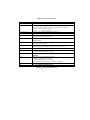
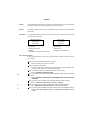
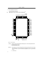
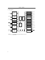
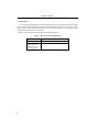
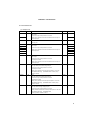
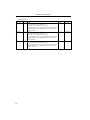
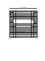
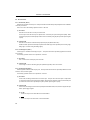
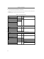
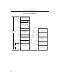
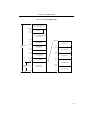
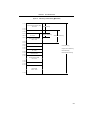
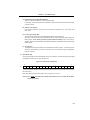
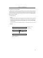
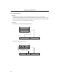
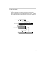
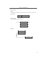
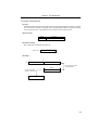
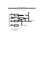
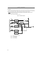
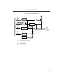
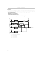
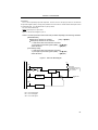
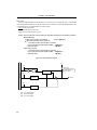
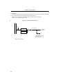
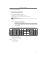
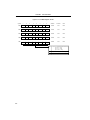
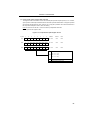
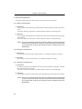
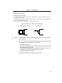
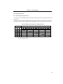
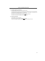
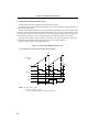
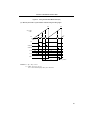
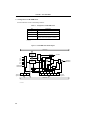
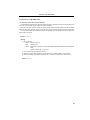
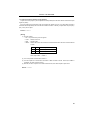
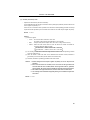
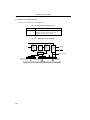
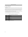
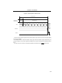
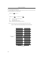
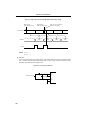
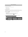
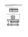
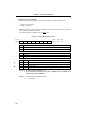
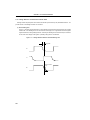
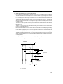
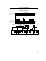
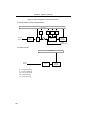
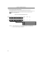
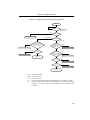
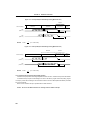
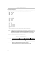
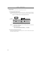
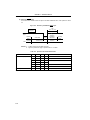
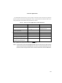
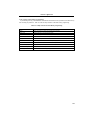
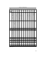
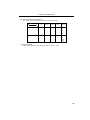
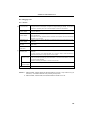
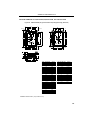
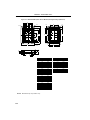
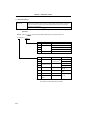
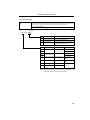
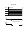
CHAPTER 11 FIP CONTROLLER/DRIVER
11.7 Calculation of Total Power Dissipation
The following three power dissipation are available for the mPD780208 subseries. The sum of the three power
dissipation should be less than the total power dissipation PT (refer to Figure 11-10) (80 % or less of ratings is
recommended).
<1> CPU power dissipation: Calculate VDD (MAX.) ¥ IDD (MAX.).
<2> Output pin power dissipation: Power dissipation when maximum current flows into each FIP output pin.
<3> Pull-down resistor power dissipation: Power dissipation by pull-down resistor incorporated in FIP output pin.
Total power dissipation PT [mW]
Figure 11-10. Total Power Dissipation PT (TA = –40 to +85 °C)
800
600
400
200
–40
0
+40
+80
Temperature [°C]
The following is how to calculate total power dissipation for the example in Figure 11-11.
Example Assume the following conditions:
VDD = 5.5 V, 5.0 MHz oscillation
Supply current (IDD) = 21.0 mA
FIP output: 11 grids ¥ 10 segments (Blanking width = 1/16: when FBLK0-FBLK2 = 000B)
Maximum current at the grid pin is 10 mA.
Maximum current at the segment pin is 3 mA.
At the key scan timing, FIP output pin is OFF.
FIP output voltage: grid
VOD = V DD – 2 V (voltage drop of 2 V)
segments VOD = V DD – 0.5 V (voltage drop of 0.5 V)
Fluorescant display control voltage (VLOAD ) = –35 V
Mask option pull-down resistor = 25 kW
139