1
Service Guide
Publication number 01680-97003
October 2001
For Safety information, Warranties, and Regulatory information, see the pages at the end
of the book.
© Copyright Agilent Technologies 2001
All Rights Reserved.
Agilent Technologies 1680/90-Series
Logic Analyzer
The Agilent 1680/90-Series Logic Analyzer–At a Glance
Features
Some of the main features of the Agilent 1680A,AD-Series Logic Analyzers are as
follows:
•
Standalone benchtop logic analyzer
•
Microsoft Windows® 2000 Pro operating system
•
132 data channels and 4 clock/data channels on the Agilent 1680A,AD
•
98 data channels and 4 clock/data channels on the Agilent 1681A,AD
•
64 data channels and 4 clock/data channels on the Agilent 1682A,AD
•
32 data channels and 2 clock/data channels on the Agilent 1683A,AD
•
12.1-inch LCD display
•
3.5-inch flexible disk drive
•
15GB hard disk drive
•
Centronics and LAN interfaces
•
IEEE 1394 interface for hosted control
•
Variable setup/hold time
•
512K acquisition memory in the Agilent 1680A-series
•
2M acquisition memory in the Agilent 1680AD-series
•
Marker Measurements
•
PS/2 Mouse
•
PS/2 keyboard support
Some of the main features of the Agilent 1690A,AD-Series Logic Analyzers are as
follows:
•
Hosted benchtop logic analyzer
•
132 data channels and 4 clock/data channels on the Agilent 1690A,AD
•
98 data channels and 4 clock/data channels on the Agilent 1691A,AD
•
64 data channels and 4 clock/data channels on the Agilent 1692A,AD
•
32 data channels and 2 clock/data channels on the Agilent 1693A,AD
•
IEEE 1394 interface for hosted control
•
Variable setup/hold time
•
512K acquisition memory in the Agilent 1690A-series
•
2M acquisition memory in the Agilent 1690AD-series
•
Marker Measurements
2
Service Strategy
The service strategy for this instrument is the replacement of defective
assemblies. This service guide contains information for finding a defective
assembly by testing and servicing the Agilent 1680/90-series logic analyzers.
This logic analyzer can be returned to Agilent for all service work, including
troubleshooting. Contact your nearest Agilent Technologies Sales Office for
details.
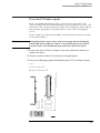
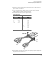
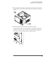
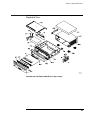
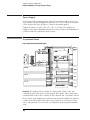
Agilent Technologies 1680-Series Logic Analyzer
Agilent Technologies 1690-Series Logic Analyzer
3
In This Book
This book is the service guide for the Agilent 1680/90-Series Logic Analyzers and
is divided into eight chapters.
Chapter 1 contains information about the logic analyzer and includes accessories,
specifications and characteristics, and equipment required for servicing.
Chapter 2 tells how to prepare the logic analyzer for use.
Chapter 3 gives instructions on how to test the performance of the logic analyzer.
Chapter 4 contains calibration instructions for the logic analyzer.
Chapter 5 contains self-tests and flowcharts for troubleshooting the logic
analyzer.
Chapter 6 tells how to replace assemblies of the logic analyzer and how to return
them to Agilent Technologies.
Chapter 7 lists replaceable parts, shows an exploded view, and gives ordering
information.
Chapter 8 explains how the logic analyzer works and what the self-tests are
checking.
4
Contents
The Agilent 1680/90-Series Logic Analyzer–At a Glance
Features 2
Service Strategy
3
In This Book
1 General Information
Accessories 10
Specifications 11
Characteristics 11
Recommended Test Equipment
14
2 Preparing for Use
Power Requirements 16
Operating Environment 16
Storage 16
To inspect the logic analyzer 16
To apply power 17
To connect the 1690A,AD-series logic analyzer to a host PC
To start the user interface 18
To clean the logic analyzer 18
To test the logic analyzer 18
17
3 Testing Performance
The Logic Analyzer Interface 20
Test Strategy 20
Test Interval 20
Performance Test Record 20
Test Equipment 20
To make the test connectors
21
To set up the test equipment and the logic analyzer
23
Set up the test equipment 23
Set up the 1680A,AD-series logic analyzer 24
Set up the 1690A,AD-series logic analyzer 25
To perform the logic analyzer self-tests 25
5
Contents
To test the threshold accuracy
27
Set up the equipment 27
Connect and configure the logic analyzer
Test the ECL Threshold 29
Test the 0 V User Threshold 30
Test the next pod 31
28
To set up the logic analyzer for the state mode tests
To test the single-clock, single-edge, state acquisition
Set up the equipment 36
Connect and configure the logic analyzer 36
Verify the test signal 39
Check the setup/hold combination 40
Test the next channels (1680/81A,AD and 1690/91A,AD)
To test the multiple-clock state acquisition
32
36
46
47
Set up the equipment 47
Connect and configure the logic analyzer 47
Verify the test signal 50
Check the setup/hold with single clock edges, multiple clocks 51
Test the next channels (1680/81A, AD and 1690/91A, AD) 55
To test the single-clock, multiple-edge, state acquisition
56
Set up the equipment 56
Connect and configure the logic analyzer 57
Verify the test signal 59
Check the setup/hold with single clock, multiple clock edges 60
Test the next channels (1680/81A,AD and 1690/91A,AD) 63
To test the time interval accuracy
64
Set up the equipment 64
Connect and configure the logic analyzer
Acquire and verify the test data 67
Performance Test Record
69
4 Calibrating and Adjusting
Logic analyzer calibration 74
6
65
Contents
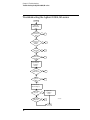
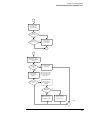
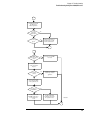
5 Troubleshooting
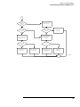
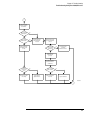
To install the fan guard 76
To use the flowcharts 77
Troubleshooting the Agilent 1680A,AD-series
78
To check the power-up tests 85
To test the power supply voltages 85
To test the LCD display signals 87
To test disk drive voltages 88
To verify the CD-ROM 90
To recover the operating system 91
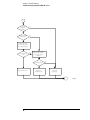
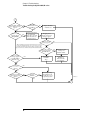
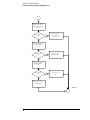
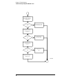
Troubleshooting the Agilent 1690A,AD-series
To verify connectivity 97
To test the power supply voltages
General Troubleshooting
93
98
100
To run the self-tests 100
Acquisition board status LEDs 102
To test the logic analyzer probe cables 103
To check the BNC Trigger input/output signals
To test the auxiliary power 108
106
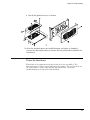
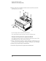
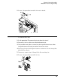
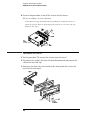
6 Replacing Assemblies
1680A,AD-series disassembly/assembly
110
Prepare the instrument for disassembly 110
To remove the chassis from the sleeve 110
To remove the acquisition board 111
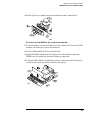
To remove the power supply 113
To remove the hard disk drive 114
To remove the CD-ROM drive 115
To remove the flexible disk drive 116
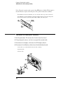
To remove the PCI boards 118
To remove the motherboard 119
To remove the front panel assembly 122
To disassemble the front panel assembly 124
To remove the distribution board 125
To remove the inverter board 126
To remove the fans 127
To remove the cable tray 128
7
Contents
1690A,AD-series disassembly/assembly
129
Prepare the instrument for disassembly 129
To remove the chassis from the sleeve 129
To remove the fascia 130
To remove the acquisition board 132
To remove the deck 133
To remove the power supply 133
To remove the distribution board 134
To remove the fans 135
To remove the line filter 136
To remove the front panel and front frame 137
7 Replaceable Parts
Replaceable Parts Ordering 140
Replaceable Parts List 141
Exploded View 142
Agilent 1680A,AD-Series Replaceable Parts 143
Exploded View 149
Agilent 1690A,AD-Series Replaceable Parts 150
Power Cables and Plug Configurations 154
8 Theory of Operation
Block-Level Theory
158
Agilent 1680A,AD-series Logic Analyzer Theory
Power Supply 160
Acquisition Board 160
Power Distribution Board
Front Panel Board 163
163
Agilent 1690A,AD-series Logic Analyzer Theory
Acquisition Board 164
Power Supply 164
Power Distribution Board
164
Self-Tests Descriptions
165
Power-up Self-Tests (1680A,AD-series) 165
Connectivity Tests (1690A,AD-series) 165
Acquisition Board Self Tests 166
Logic Analyzer Self-Tests 167
8
159
164
1
General Information
This chapter lists the accessories, the specifications and characteristics, and the
recommended test equipment.
9
Chapter 1: General Information
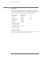
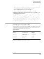
Accessories
The following accessories are supplied with the Agilent 1680/90-series logic
analyzers. The part numbers are current as of the print date of this edition of the
Service Guide, but further upgrades may change the part numbers. Do not be
concerned if the accessories you receive have different part numbers.
$FFHVVRULHV6XSSOLHG
$JLOHQW3DUW1XPEHU
4W\
3UREHWLSDVVHPEOLHV
3UREHFDEOHV
*UDEEHUVSHUSDFN
3UREHJURXQGSHUSDFN
'RXEOH3UREH$GDSWHU
360RXVH
&
1RWH
1RWH
1RWH
1RWH
Note 1 Quantities:8 - 1680A,AD or 1690A,AD
6 - 1681A,AD or 1691A,AD
4 - 1682A,AD or 1692A,AD
2 - 1683A,AD or 1693A,AD
Note 2 Quantities:4 - 1680A,AD or 1690A,AD
3 - 1681A,AD or 1691A,AD
2 - 1682A,AD or 1692A,AD
1 - 1683A,AD or 1693A,AD
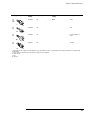
Accessories Available
Other accessories available for the Agilent 1680/90-series logic analyzer are listed
in the Accessories for Agilent Logic Analyzers brochure.
10
Chapter 1: General Information
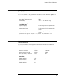
Specifications
The specifications are the performance standards against which the product is
tested.
0D[LPXP6WDWH6SHHGVHOHFWDEOH
0LQLPXP0DVWHUWR0DVWHU&ORFN7LPH
7KUHVKROG$FFXUDF\
0+]
QV
P9RIWKUHVKROGVHWWLQJ
Setup/Hold Time*
6LQJOH&ORFN6LQJOH(GJH
QVWKURXJKQVDGMXVWDEOHLQSV
LQFUHPHQWV
6LQJOH&ORFN0XOWLSOH(GJHV
QVWKURXJKQVDGMXVWDEOHLQSV
LQFUHPHQWV
0XOWLSOH&ORFNV0XOWLSOH(GJHV
QVWKURXJKQVDGMXVWDEOHLQSV
LQFUHPHQWV
6SHFLILHGIRUDQLQSXWVLJQDO9+ −99/ −9VOHZUDWH 9QVDQGWKUHVKROG −9
Characteristics
These characteristics are not specifications, but are included as additional
information.
0D[LPXP6WDWH&ORFN5DWH
0D[LPXP&RQYHQWLRQDO7LPLQJ5DWH
0HPRU\'HSWK$RU$VHULHV
0HPRU\'HSWK$'RU$'VHULHV
)XOO&KDQQHO
+DOI&KDQQHO
0+]
0+]
.
.
QRWDSSOLFDEOH
0+]
.
.
&KDQQHO&RXQW
$$'RU$$'
$$'RU$$'
$$'RU$$'
$$'RU$$'
11
Chapter 1: General Information
Probes
Maximum Input Voltage + 40V Peak AC+DC, CAT 1
Auxiliary Power
Power Through Cables 1/3 amp at 5 V maximum per cable, CAT 1
Operating Environment (for indoor use only)
Temperature: Instrument, 0 C to 55 C (+32 F to 131 F).
Probe lead sets and cables,
0 C to 65 C (+32 F to 149 F).
Disk media, 10 C to 40 C (+50 F to 104 F).
Humidity: Instrument, probe lead sets, and cables, up to
80% relative humidity at +40 C (+122 F).
Altitude: To 3067 m (10,000 ft).
Vibration Operating: Random vibration 5 to 500 Hz,
10 minutes per axis, 0.3 g (rms).
Non-operating: Random vibration 5 to 500 Hz,
10 minutes per axis, 2.41 g (rms);
and swept sine resonant search, 5 to 500 Hz,
0.75 g (0-peak), 5 minute resonant dwell
at 4 resonances per axis.
12
Chapter 1: General Information
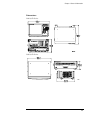
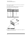
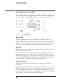
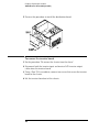
Dimensions
1680A,AD-Series
1690A,AD-Series
13
Chapter 1: General Information
Recommended Test Equipment
Equipment Required
(TXLSPHQW
&ULWLFDO6SHFLILFDWLRQV
5HFRPPHQGHG0RGHO3DUW
8VH
3XOVH*HQHUDWRU
0+]QVSXOVHZLGWK
<SVULVHWLPH
$2SWLRQ
37
'LJLWL]LQJ2VFLOORVFRSH
≥*+]EDQGZLGWK
<SVULVHWLPH
$PDLQIUDPHZLWK$ 3
SOXJLQPRGXOH
)XQFWLRQ*HQHUDWRU
$FFXUDF\ IUHTXHQF\
'&RIIVHWYROWDJH±9
$
3
'LJLWDO0XOWLPHWHU
P9UHVROXWLRQ
DFFXUDF\
$
3
3
%1&7HH
%1&PII
3
&DEOH
%1&PPLQFK
37
60$&RD[&DEOH4W\
*+]EDQGZLGWK
3
%1&%DQDQD&DEOH
$GDSWHU4W\
60$P%1&I
37
$GDSWHU
60$I%1&P
3
&RXSOHU4W\
%1&PP
37
$
3
$
7
3UREHV4W\
%1&&RD[&DEOH
%1&PP!*+]
EDQGZLGWK!PHWHUOHQJWK
%1&7HVW&RQQHFWRU[4W\
3
%1&7HVW&RQQHFWRU[4W\
37
'LJLWL]LQJ2VFLOORVFRSH
!0+]%DQGZLGWK
%
7
%1&6KRUWLQJ&DS
7
%1&%DQDQD$GDSWHU
7
$ $GMXVWPHQW3 3HUIRUPDQFH7HVWV7 7URXEOHVKRRWLQJ
,QVWUXFWLRQVIRUPDNLQJWKHVHWHVWFRQQHFWRUVDUHLQFKDSWHU7HVWLQJ3HUIRUPDQFH
14
2
Preparing for Use
This chapter gives you instructions for preparing the logic analyzer for use.
15
Chapter 2: Preparing for Use
Power Requirements
The logic analyzer requires a power source of either 115 Vac or 230 Vac, –22 % to
+10 %, single phase, 48 to 66 Hz, CAT II pollution degree 2, 140/400 Watts
nominal maximum power (1680A/AD-series), and 76/200 Watts nominal
maximum power (1690A/AD-series).
Operating Environment
The operating environment is listed in chapter 1. The logic analyzer will operate
at all specifications within the temperature and humidity range given in chapter
1. However, reliability is enhanced when operating the logic analyzer within the
following ranges:
•
Temperature: +20 C to +35 C (+68 F to +95 F)
•
Humidity: 20% to 80% noncondensing
Note the recommended noncondensing humidity. Condensation within the
instrument can cause poor operation or malfunction. Provide protection against
internal condensation.
Storage
Store or ship the logic analyzer in environments within the following limits:
•
Temperature: -40 C to +75 C
•
Humidity: Up to 90% at 65 C
•
Altitude: Up to 15,300 meters (50,000 feet)
Protect the logic analyzer from temperature extremes which cause condensation
on the instrument.
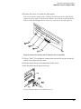
To inspect the logic analyzer
1 Inspect the shipping container for damage.
If the shipping container or cushioning material is damaged, keep them until you
have checked the contents of the shipment and checked the instrument
mechanically and electrically.
2 Check the supplied accessories.
Accessories supplied with the logic analyzer are listed in "Accessories" in chapter
1.
16
Chapter 2: Preparing for Use
3 Inspect the product for physical damage.
Check the logic analyzer and the supplied accessories for obvious physical or
mechanical defects. If you find any defects, contact your nearest Agilent
Technologies Sales Office. Arrangements for repair or replacement are made, at
Agilent Technologies’ option, without waiting for a claim settlement.
To apply power
These steps are required for all 1680A,AD and 1690A,AD-series logic analyzers.
1 Connect the power cord to the instrument and to the power source.
This instrument autodetects the line voltage from 115 VAC to 230 VAC. It is
equipped with a three-wire power cable. When connected to an appropriate AC
power outlet, this cable grounds the instrument cabinet. The type of power cable
plug shipped with the instrument depends on the country of destination. Refer to
chapter 7, "Replaceable Parts," for option numbers of available power cables.
2 Turn on the power switch located on the front panel.
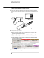
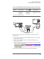
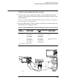
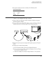
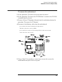
To connect the 1690A,AD-series logic analyzer to a host PC
These steps are required for the Agilent 1690A,AD-series hosted logic analyzer.
The logic analyzer user interface requires a host computer (PC) with the
following characteristics (or better):
Intel Celeron, AMD K6-II 500 MHz
Windows 2000 Professional
128MB RAM
IEEE 1394 PCI card
1 Connect one end of the 6-pin IEEE 1394 cable to the IEEE 1394 port on
the host PC.
2 Connect the free end of the IEEE 1394 cable to the IEEE 1394 port on the
logic analyzer.
3 Apply power to the PC if it is not turned on.
17
Chapter 2: Preparing for Use
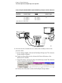
To start the user interface
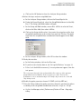
Start the Agilent Logic Analyzer application from the Start menu or using a
shortcut. On the desktop, the Agilent Logic Analyzer icon looks like:
Refer to the Agilent Logic Analyzer on-line help for information on how to
operate the user interface. Also, refer to the window icon reference on the inside
front cover of this service manual for a brief explanation of the Agilent Logic
Analyzer standard icons.
To clean the logic analyzer
With the instrument turned off and unplugged, use mild soap and water to clean
the front and cabinet of the logic analyzer. Harsh soap might damage the waterbase paint.
To test the logic analyzer
• If you require a test to verify the specifications, start at the beginning of
chapter 3, "Testing Performance."
• If you require a test to initially accept the operation, perform the self-tests
in chapter 3.
• If the logic analyzer does not operate correctly, go to the beginning of
chapter 5, "Troubleshooting."
18
3
Testing Performance
This chapter tells you how to test the performance of the logic analyzer against
the specifications listed in chapter 1.
19
Chapter 3: Testing Performance
The Logic Analyzer Interface
To select a field on the logic analyzer screen, use the arrow keys to highlight the
field, then press the Select key. Provided on the inside front cover of this manual
is a list of logic analyzer icons that can be referenced while performing test
procedures. For more information about the logic analyzer interface, refer to the
Agilent Logic Analyzer On-line Help System.
Test Strategy
For a complete test, start at the beginning with the software tests and continue
through to the end of the chapter. For an individual test, follow the procedure in
the test. The examples in this chapter were performed using an Agilent 1680AD.
Other analyzers in the series will have appropriate pods showing on the screen.
The performance verification procedures starting on page 3–8 are each shown
from power-up. To exactly duplicate the setups in the tests, save the power-up
configuration to a file on a disk, then load that file at the start of each test.
If a test fails, check the test equipment setup, check the connections, and verify
adequate grounding. If a test still fails, the most probable cause of failure would
be the acquisition board.
Test Interval
Test the performance of the logic analyzer against specifications at two-year
intervals.
Performance Test Record
A performance test record for recording the results of each procedure is located
at the end of this chapter. Use the performance test record to gauge the
performance of the logic analyzer over time.
Test Equipment
Each procedure lists the recommended test equipment. You can use equipment
that satisfies the specifications given. However, the procedures are based on
using the recommended model or part number. Before testing the performance
of the logic analyzer, warm-up the instrument and the test equipment for 30
minutes.
20
Chapter 3: Testing Performance
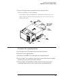
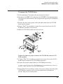
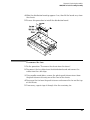
To make the test connectors
To make the test connectors
The test connectors connect the logic analyzer to the test equipment.
Materials Required
'HVFULSWLRQ
5HFRPPHQGHG3DUW
4W\
%1&I&RQQHFWRU
ΩUHVLVWRU
%HUJ6WULSE\
%HUJ6WULSE\
3UREH
$
-XPSHUZLUH
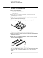
1 Build four test connectors using BNC connectors and 6-by-2 sections of
Berg strip.
a Solder a jumper wire to all pins on one side of the Berg strip.
b Solder a jumper wire to all pins on the other side of the Berg strip.
c Solder two resistors to the Berg strip, one at each end between the end
pins.
d Solder the center of the BNC connector to the center pin of one row on
the Berg strip.
e Solder the ground tab of the BNC connector to the center pin of the
other row on the Berg strip.
21
Chapter 3: Testing Performance
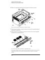
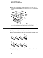
To make the test connectors
f On two of the test connectors, solder a 20:1 probe. The probe ground
goes to the same row of pins on the test connector as the BNC ground
tab.
2 Build one test connector using a BNC connector and a 17-by-2 section of
Berg strip.
a Solder a jumper wire to all pins on one side of the Berg strip.
b Solder a jumper wire to all pins on the other side of the Berg strip.
c Solder the center of the BNC connector to the center pin of one row on
the Berg strip.
d Solder the ground tab of the BNC connector to the center pin of the
other row on the Berg strip.
22
Chapter 3: Testing Performance
To set up the test equipment and the logic analyzer
To set up the test equipment and the logic analyzer
Before testing the specifications of the Agilent 1680A,AD-series or 1690A,ADseries logic analyzer, the test equipment and the logic analyzer must be set up
and configured.
These instructions include detailed steps for initially setting up the required test
equipment and the logic analyzer. Before performing any or all of the tests in this
chapter, the following steps must be done.
Equipment Required
5HFRPPHQGHG+3$JLOHQW
0RGHO3DUW
(TXLSPHQW
&ULWLFDO6SHFLILFDWLRQV
3XOVH*HQHUDWRU
0K]QVSXOVHZLGWKSVULVHWLPH $RSWLRQ
'LJLWL]LQJ2VFLOORVFRSH ≥*+]EDQGZLGWKSVULVHWLPH
$Z$
'LJLWDO0XOWLPHWHU
P9UHVROXWLRQDFFXUDF\
$
)XQFWLRQ*HQHUDWRU
'&RIIVHWYROWDJH9
%2SWLRQ
Set up the test equipment
1 Turn on the required test equipment listed in the table above. Let them
warm up for 30 minutes before beginning any test.
2 Set up the pulse generator according to the following table.
Pulse Generator Setup
7LPHEDVH
&KDQQHO
7ULJJHU
&KDQQHO
0RGH,QW
3HULRGQV
0RGH3XOVH
'LYLGH3XOVH÷ :LGWKQV
$PSO9
2IIV9
&203'LVDEOHG
/('2II
'LYLGH'LYLGH÷ $PSO9
2IIV9
0RGH6TXDUH
'HOD\SV
$PSO9
2IIV9
&203'LVDEOHG
/('2II
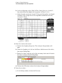
3 Set up the oscilloscope.
a Select Setup, then select Default Setup.
23
Chapter 3: Testing Performance
To set up the test equipment and the logic analyzer
b Configure the oscilloscope according to the following table.
Oscilloscope Setup
$FTXLVLWLRQ
'LVSOD\
7ULJJHU
>6KLIW@∆7LPH
$YHUDJLQJ2Q
RIDYHUDJHV
*UDWLFXOHJUDSKV
/HYHO9
6WRSVUFFKDQQHO>(QWHU@
&KDQQHO
&KDQQHO
'HILQHPHDV
([WHUQDO6FDOH
$WWHQXDWLRQ
6FDOHP9GLY
2IIVHW9
([WHUQDO6FDOH
$WWHQXDWLRQ
6FDOHP9GLY
2IIVHW9
7KUHVKROGVXVHUGHILQHG
8QLWV9ROWV
8SSHUP9
0LGGOH9
/RZHU9
Set up the 1680A,AD-series logic analyzer
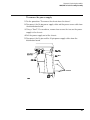
Power-up self tests are done on the logic analyzer system components when
power is applied. Any problems reported by the logic analyzer during boot must
be cleared before going further. For more information, refer to Chapter 5 and
Chapter 8.
1 Turn on the logic analyzer.
a Connect a keyboard and mouse to the rear panel of the logic analyzer.
b Plug in a power cord to the rear panel power connector of the logic
analyzer.
c Turn on the power switch on the logic analyzer front panel.
2 Set up the logic analyzer.
a Wait for the logic analyzer boot up to complete.
b On the logic analyzer desktop, double-click the Agilent Logic Analyzer
icon to launch the logic analyzer application.
24
Chapter 3: Testing Performance
To set up the test equipment and the logic analyzer
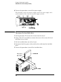
Set up the 1690A,AD-series logic analyzer
Power-up self tests are done on the logic analyzer system components when
power is applied. Logic analyzer peripheral communication tests are done when
the host PC recognizes the hosted logic analyzer hardware. Any problems
reported should be cleared before going further. For more information, refer to
Chapter 5 and Chapter 8.
1 Connect the logic analyzer to the host PC.
2 Set up the logic analyzer.
a Wait for the logic analyzer power-up to complete.
b On the host PC desktop, double-click the Agilent Logic Analyzer icon to
launch the logic analyzer application.
c In the Agilent Logic Analyzer application window, ensure the
application reports “Online.”
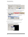
To perform the logic analyzer self-tests
The self-tests verify the correct operation of the logic analyzer. Self-tests can be
performed all at once or one at a time. While testing the performance of the logic
analyzer, run the self-tests all at once. Refer to Chapter 8 for more information on
the logic analyzer self-tests.
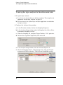
1 In the Agilent Logic Analyzer application window, click on Help. At the
pop-up window, click on Self Test, then select Analyzer Self Test.
NOTE:
The warning dialog box is normal, click OK to continue.
25
Chapter 3: Testing Performance
To set up the test equipment and the logic analyzer
The Logic Analyzer Self Test window will appear.
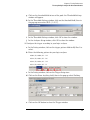
2 In the Logic Analyzer Self Test window, click on the Run All Tests button.
The pass/fail status of each test is reported as the test completes. When all self
tests are complete, a summary is printed in the status window concluding with
“All Tests PASSED!” or with test failure information. Report the PASS/FAIL status
in the Performance Test Record.
3 In the Logic Analyzer Self Test window, click Close to close the window.
26
Chapter 3: Testing Performance
To test the threshold accuracy
To test the threshold accuracy
Testing the threshold accuracy verifies the performance of the following
specification:
•
Clock and data channel threshold accuracy.
These instructions include detailed steps for testing the threshold settings of
pod 1. After testing pod 1, connect and test the rest of the pods one at a time. To
test the next pod, follow the detailed steps for pod 1, substituting the next pod
for pod 1 in the instructions.
Each threshold test tells you to record a pass/fail reading in the performance test
record located at the end of this chapter.
Equipment Required
(TXLSPHQW
&ULWLFDO6SHFLILFDWLRQV
5HFRPPHQGHG0RGHO3DUW
'LJLWDO0XOWLPHWHU
P9UHVROXWLRQDFFXUDF\
$
)XQFWLRQ*HQHUDWRU
$FFXUDF\ IUHTXHQF\
'&RIIVHWYROWDJH±9
$
%1&%DQDQD&DEOH
%1&7HH
%1&&DEOH
%1&7HVW&RQQHFWRU[
Set up the equipment
1 If you have not already done so, do the procedure “To set up the test
equipment and the logic analyzer” on page 23.
2 Set up the DC source to deliver a DC voltage on the output.
a In the function generator Utility menu, activate the DC Level. All AC
voltage functions will be disabled.
b Enable the high impedance load under the Output Setup menu.
3 Using a BNC-banana cable, connect the voltmeter to one side of the BNC
Tee.
4 Connect the BNC Tee to the output of the DC source. Set up the logic
analyzer
27
Chapter 3: Testing Performance
To test the threshold accuracy
Connect and configure the logic analyzer
1 Using the 17-by-2 test connector, BNC cable, and probe tip assembly,
connect the data and clock channels of Pod 1 to the free side of the BNC
Tee.
2 Configure the logic analyzer.
a In the Waveform window, click on the Bus/Signal Setup icon. The
Analyzer Setup window will open.
b Under the Buses/Signals tab, click on the Delete All button at the
bottom of the window.
c Using the mouse, activate all Pod 1 channels. The channels will be
assigned to label My Bus 1.
d Scroll the channel assignments to the left. Assign the clock/data
channel for the Pod 1 (that is, C1) to the label My Bus 1.
3 Activate the DC source output.
28
Chapter 3: Testing Performance
To test the threshold accuracy
Test the ECL Threshold
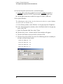
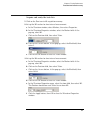
1 Set up the logic analyzer.
a In the Analyzer Setup window, click on the threshold field for Pod 1.
The Threshold Settings window will appear.
b In the threshold Settings window, select the threshold voltage field. In
the pop-up, select ECL (–1.30 V).
c In the Threshold Settings window, click OK to close the window.
d In the Analyzer Setup window, click OK to close the window.
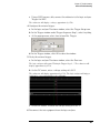
2 Test the high-to-low transition.
a On the DC source, enter a voltage setting of –1.384 V.
b On the logic analyzer, click on the Run icon. The display should show all
channels at a logic "0"
.
3 Test the low-to-high transition.
a On the DC source, enter a voltage setting of –1.216 V.
b On the logic analyzer, click on the Run icon. The display should show all
channels at a logic "1" (0x1FFFF)
.
4 Record a PASS/FAIL in the performance test record for Threshold
Accuracy Pod 1 - ECL.
29
Chapter 3: Testing Performance
To test the threshold accuracy
Test the 0 V User Threshold
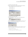
1 Set up the logic analyzer
a On the logic analyzer, click on the Bus/Signal Setup icon. The Analyzer
Setup window will open.
b In the Analyzer Setup window, click on the threshold field for Pod 1.
The Threshold Settings window will appear.
c In the Threshold Settings window, select the threshold voltage field. In
the pop-up, select User.
d If the user-defined voltage field does not read 0 V, click on the userdefined voltage field and enter 0.
e In the Threshold Settings window, click OK to close the window.
f In the Analyzer Setup window, click OK to close the window.
2 Test the high-to-low transition.
a On the DC source, enter a voltage setting of –0.064 V.
b On the logic analyzer, click on the Run icon. The display should show all
channels at a logic "0".
3 Test the low-to-high transition.
a On the DC source, enter a voltage setting of 0.064 V.
b On the logic analyzer, click on the Run icon. The display should show all
channels at a logic "1" (0x1FFFF).
4 Record a PASS/FAIL in the performance test record for Threshold
Accuracy Pod 1 - User 0 V.
30
Chapter 3: Testing Performance
To test the threshold accuracy
Test the next pod
1 Using the 17-by-2 test connector and probe tip assembly, connect the data
and clock channels of the next pod to the output of the function generator
until all pods have been tested.
2 Start with “Connect and configure the logic analyzer” on page 28
substituting the next pod to be tested for pod 1.
31
Chapter 3: Testing Performance
To set up the logic analyzer for the state mode tests
To set up the logic analyzer for the state mode tests
1 Set up the logic analyzer.
a If you have not already done so, do the procedure “To set up the test
equipment and the logic analyzer” on page 23.
b Exit and restart the Agilent Logic Analyzer application to reinitialize
the logic analyzer.
2 Configure the Analyzer Setup window.
a In the Waveform window, click on the Sampling Setup icon.
b In the Analyzer Setup window under the Samplng tab, click on State Synchronous Sampling to select.
c Under the Sampling tab, configure Trigger Position - 100% poststore.
d Click on the Acquisition Depth field, then select 8K.
e In the Analyzer Setup window, click on the Buses/Signals tab.
f Click on the Display button. At the pop-up menu, click on Channels
Assigned and Width to deselect. Then click on Setup/Hold to select.
32
Chapter 3: Testing Performance
To set up the logic analyzer for the state mode tests
g Click on the threshold field of one of the pods. the Threshold Settings
window will appear.
h In the Threshold Settings window, click on the threshold field, then in
the pop-up menu select ECL (–1.30 V).
i In the Threshold Settings window, click OK to close the window.
j In the Analyzer Setup window, click OK to close the window.
3 Configure the trigger according to your logic analyzer.
a In the Listing window, click on the trigger pattern field for My Bus 1 to
select.
b Enter the following pattern for your logic analyzer.
1680A,AD, 1690A,AD - "AA"
1681A,AD, 1691A,AD - "2A"
1682A,AD, 1692A,AD - "AA"
1683A,AD, 1693A,AD - "A"
c In the Listing window, click on the Trigger Setup icon.
d Click on the Store Anything field, then in the pop-up select Nothing.
e Click on the OK button to close the Trigger window.
33
Chapter 3: Testing Performance
To set up the logic analyzer for the state mode tests
4 Activate the pulse generator data and clock outputs.
a On the pulse generator, enable the channel 1 OUTPUT, channel 1
OUTPUT, channel 2 OUTPUT and channel 2 OUTPUT (LEDs off)
b On the pulse generator, enable the trigger OUTPUT. (LED off)
5 Set up the Markers.
The following procedure is done after the first run of test data is acquired (during
one of the state clock mode tests).
a In the Listing window, select Markers. At the pop-up select Properties.
b In the Listing Properties window, select the Marker field. At the pop-up
menu, select M1.
c Select the Position field, then select Value.
d Click on the Occurs... button and the Value window will appear.
e Click on the Find occurrences field, and enter 4096.
f Click on the pattern field, then enter the following pattern according to
the logic analyzer being tested:
1680A,AD, 1690A,AD - "AA"
1681A,AD, 1691A,AD - "2A"
1682A,AD, 1692A,AD - "AA"
1683A,AD, 1693A,AD - "A"
34
Chapter 3: Testing Performance
To set up the logic analyzer for the state mode tests
g Click OK to close the Value window.
h Repeat steps b through f to configure marker M2 using the following
pattern according to the logic analyzer being tested.
1680A,AD, 1690A,AD - "55"
1681A,AD, 1691A,AD - "15"
1682A,AD, 1692A,AD - "55"
1683A,AD, 1693A,AD - "5"
i Click OK to close the Value window.
j In the Listing Properties window, select the from field, then select
Beginning of Data.
The logic analyzer markers are now configured to verify the test data. If the error
message "can’t find 4096 occurence(s)" does not appear, then the test passes.
Click OK to close the Listing Properties window
When the above error message appears, then one or more samples of test data is
incorrect. When this happens, check the following and attempt the test again:
•
all cables are properly connected
•
configuration of each test equipment is correct
•
logic analyzer is properly set up according to the test procedure
35
Chapter 3: Testing Performance
To test the single-clock, single-edge, state acquisition
To test the single-clock, single-edge, state acquisition
Testing the single-clock, single-edge, state acquisition verifies the performance of
the following specifications:
•
Minimum master-to-master clock time
•
Maximum state acquisition speed
•
Setup/Hold time for single-clock, single-edge, state acquisition
This test checks two combinations of data channels using a single-edge clock at
two selected setup/hold times.
Equipment Required
(TXLSPHQW
&ULWLFDO6SHFLILFDWLRQV
5HFRPPHQGHG0RGHO3DUW
3XOVH*HQHUDWRU
0+]QVSXOVHZLGWK<SVULVHWLPH $RSWLRQ
'LJLWL]LQJ2VFLOORVFRSH
≥*+]EDQGZLGWK<SVULVHWLPH
$Z$
$GDSWHU
60$P%1&I
60$&RD[&DEOH4W\
*+]EDQGZLGWK
&RXSOHU
%1&PP
%1&7HVW&RQQHFWRU
[4W\
Set up the equipment
If you have not already done so, do the following procedures:
“To set up the test equipment and the logic analyzer” on page 23.
“To set up the logic analyzer for the state mode tests” on page 32.
Connect and configure the logic analyzer
1 Using the 6-by-2 test connectors, connect the first combination of logic
analyzer clock and data channels listed in one of the following tables to the
pulse generator.
If you are testing an Agilent 1680/81/90A,AD or Agilent 1691A,AD, you will repeat
this test for the second combination.
36
Chapter 3: Testing Performance
To test the single-clock, single-edge, state acquisition
2 Using SMA cables, connect the oscilloscope to the pulse generator channel
1 Output, channel 2 Output, and Trigger Output.
Connect the Agilent 1680/81/90A,AD or Agilent 1691A,AD Logic Analyzer to the Pulse Generator
7HVWLQJ
&RPELQDWLRQV
&RQQHFWWR$
&KDQQHO2XWSXW
&RQQHFWWR$
&KDQQHO2XWSXW
&RQQHFWWR$
&KDQQHO2XWSXW
3RGFKDQQHO
3RGFKDQQHO
3RGFKDQQHO
3RGFKDQQHO
3RGFKDQQHO
3RGFKDQQHO
3RGFKDQQHO
3RGFKDQQHO
3RGFORFNGDWDFKDQQHO&ON
3RGFKDQQHO
3RGFKDQQHO
3RGFKDQQHO
3RGFKDQQHO
3RGFKDQQHO
3RGFKDQQHO
3RGFKDQQHO
3RGFKDQQHO
3RGFORFNGDWDFKDQQHO&ON
$JLOHQW$$'RU$JLOHQW$$'RQO\
37
Chapter 3: Testing Performance
To test the single-clock, single-edge, state acquisition
Connect the Agilent 1682/83/92A,AD or Agilent 1693A,AD Logic Analyzer to the Pulse Generator
7HVWLQJ
&RPELQDWLRQ
&RQQHFWWR$
&KDQQHO2XWSXW
&RQQHFWWR$
&KDQQHO2XWSXW
&RQQHFWWR$
&KDQQHO2XWSXW
3RGFKDQQHO
3RGFKDQQHO
3RGFKDQQHO
3RGFKDQQHO
3RGFKDQQHO
3RGFKDQQHO
3RGFKDQQHO
3RGFKDQQHO
3RGFORFNGDWDFKDQQHO&ON
$JLOHQW $$'RU$JLOHQW$$'RQO\
3 Activate the data channels that are connected according to one of the
previous tables.
a In the Listing window, click on the Bus/Signal Setup icon. The Analyzer
Setup window will open.
b Under the Buses/Signals tab, click on the Delete All button at the
bottom of the window.
c Using the mouse, activate the data channels being tested. The channels
will be assigned to label My Bus 1.
d Click on the OK button to close the Bus/Signal Setup window.
38
Chapter 3: Testing Performance
To test the single-clock, single-edge, state acquisition
Verify the test signal
1 Check the clock period. Using the oscilloscope, verify that the master-tomaster clock time is 5.000 ns, +0 ps or −100 ps.
a In the oscilloscope Timebase menu, select Scale: 1.000 ns/div.
b In the oscilloscope Timebase menu, select Position. Using the
oscilloscope knob, position the clock waveform so that a rising edge
appears at the left of the display.
c On the oscilloscope, select [Shift] Period: channel 2, then select [Enter]
to display the clock period (Period(2)). If the period is not less than
5.000 ns, go to step d. If the period is less than 5.000 ns, go to step 2.
d In the oscilloscope Timebase menu, increase Position 5.000 ns. If the
period is not less than 5.000 ns, decrease the pulse generator Period in
until one of the two periods measured is less than 5.000 ns.
2 Check the data pulse width. Using the oscilloscope, verify that the data
pulse width is 2.500 ns, +0 ps or −100 ps.
a In the oscilloscope Timebase menu, select Position. Using the
oscilloscope knob, position the data waveform so that the waveform is
centered on the screen.
b On the oscilloscope, select [Shift] + width: channel 1, then select
[Enter] to display the data signal pulse width (+ width(1)).
39
Chapter 3: Testing Performance
To test the single-clock, single-edge, state acquisition
c If the pulse width is outside the limits, adjust the pulse generator
channel 2 width until the pulse width is within limits.
Check the setup/hold combination
The following setup/hold combinations will be tested:
Setup/Hold Combinations
QV
QV
1 Disable the pulse generator channel 1 COMP (with the LED off).
2 Using the Delay mode of the pulse generator channel 1, position the pulses
according to the setup time of the setup/hold combination selected, +0.0
ps or −100 ps as measured on the oscilloscope.
a On the Oscilloscope, select [Define meas] Define ∆ Time - Stop edge:
rising, Edge number 2.
b In the oscilloscope timebase menu, select Position. Using the
oscilloscope knob, position the data waveform so the falling edge is near
the center of the display.
40
Chapter 3: Testing Performance
To test the single-clock, single-edge, state acquisition
c On the oscilloscope, select [Shift] ∆ Time, then select [Enter] to display
the setup time (∆ Time(1)-(2)).
d Adjust the pulse generator channel 1 Delay until the pulses are aligned
according to the setup time of the setup/hold combination selected,
+0.0 ps or –100 ps.
3 Select the logic analyzer setup/hold time.
a Click on the Bus/Signal Setup icon. The Analyzer Setup window will
open.
b Under the Buses/Signal tab, select the Setup/Hold field next to label My
Bus 1. The Setup and Hold window will open.
c In the Setup and Hold window, ensure Bits: All Bits is selected. If not,
click on the Bits: field, then select All Bits.
41
Chapter 3: Testing Performance
To test the single-clock, single-edge, state acquisition
d Click on the Setup field to select, then enter the setup time of the first
setup/hold combination to be tested, then push the Tab key. The hold
time from the setup/hold time combination should appear in the Hold:
field.
e Click on the OK button to close the Setup and Hold window.
4 Select the clock to be tested.
The following clock configurations will be used in steps 4, 5 and 6.
a In the Analyzer Setup window, click on the Sampling tab.
b Under the Sampling tab, click on the Master field for the first clock to
be tested (Clk 1), then select Rising Edge.
c Click the Master field for the remaining clocks, then select Don’t Care
to turn off the other clocks.
d Connect the clock to be tested to the pulse generator channel 1 output.
42
Chapter 3: Testing Performance
To test the single-clock, single-edge, state acquisition
e Click on the OK button to close the Analyzer Setup window.
5 Verify the test data.
a In the Listing window, click on the Run icon.
b If you have not already done so, do “Set up the Markers.” on page 34.
c If the "can't find 4096 occurence(s)" message does not appear, then the
test passes.
The test passes when the logic analyzer finds all occurances of the patterns
programmed into the Markers. If the test passes, record a "Pass" in the
performance test record under single-clock single-edge next to the clock and
edge being tested.
6 Test the next clock.
a In the Listing window, click on the Sampling Setup icon.
b Disconnect the clock just tested from the pulse generator.
c Repeat steps 4, 5, and 6 for the next clock configuration listed in step 4
until all listed clock combinations have been tested.
7 Enable the pulse generator channel 1 COMP (with the LED on).
8 Using the Delay mode of the pulse generator channel 1, position the pulses
according to the setup/hold combination selected, +0.0 ps or –100 ps as
measured on the oscilloscope.
a On the Oscilloscope, select [Define meas] Define ∆ Time - Stop edge:
falling.
b On the oscilloscope, select [Shift] ∆ Time. Select Start src: channel 1,
then select [Enter] to display the setup time (∆ Time(1)-(2)).
43
Chapter 3: Testing Performance
To test the single-clock, single-edge, state acquisition
c Adjust the pulse generator channel 1 Delay until the pulses are aligned
according to the setup time of the setup/hold combination selected,
+0.0 ps or –100 ps.
9 Select the clock to be tested.
The following clock configurations will be used in steps 9, 10 and 11.
a In the Analyzer Setup window, click on the Sampling tab.
b Under the Sampling tab, click on the Master field for the first clock to
be tested (Clk 1), then select Falling Edge.
44
Chapter 3: Testing Performance
To test the single-clock, single-edge, state acquisition
c Click the Master field for the remaining clocks, then select Don’t Care
to turn off the other clocks.
d Connect the clock to be tested to the pulse generator channel 1 output.
e Click on the OK button to close the Analyzer Setup window.
10 Verify the test data.
a In the Listing window, click on the Run icon.
b If you have not already done so, do “Set up the Markers.” on page 34.
c If the "can't find 4096 occurence(s)" message does not appear, then the
test passes.
The test passes when the logic analyzer finds all occurances of the patterns
programmed into the Markers. If the test passes, record a "Pass" in the
performance test record under single-clock single-edge next to the clock and
edge being tested.
11 Test the next clock.
a In the Listing window, click on the Sampling Setup icon.
b Disconnect the clock just tested from the pulse generator.
c Repeat steps 9, 10, and 11 for the next clock configuration listed in step
9 until all listed clock combinations have been tested.
12 Test the next setup/hold combination.
a In the Listing window, click on the Bus/Signal Setup icon.
b Disconnect the clock just tested from the pulse generator.
c Repeat steps 1 through 12 for the next setup/hold combination listed on
page 40.
45
Chapter 3: Testing Performance
To test the single-clock, single-edge, state acquisition
Test the next channels (1680/81A,AD and 1690/91A,AD)
Connect the next combination of data channels and clock channels, then test
them.
Start with “Connect and configure the logic analyzer” on page 36, connect the
next combination, then continue through the complete test.
46
Chapter 3: Testing Performance
To test the multiple-clock state acquisition
To test the multiple-clock state acquisition
Testing the multiple-clock, state acquisition verifies the performance of the
following specifications:
•
Minimum master-to-master clock time
•
Maximum state acquisition speed
•
Setup/Hold time for multiple-clock, state acquisition
This test checks two combinations of data using multiple clocks at two selected
setup/hold times.
Equipment Required
(TXLSPHQW
&ULWLFDO6SHFLILFDWLRQV
5HFRPPHQGHG0RGHO3DUW
3XOVH*HQHUDWRU
0+]QVSXOVHZLGWK
<SVULVHWLPH
$RSWLRQ
'LJLWL]LQJ2VFLOORVFRSH
≥ *+]EDQGZLGWK<SVULVHWLPH
$Z$
$GDSWHU
60$P%1&I
60$&RD[&DEOH4W\
*+]EDQGZLGWK
&RXSOHU
%1&PP
%1&7HVW&RQQHFWRU
[4W\
Set up the equipment
1 If you have not already done so, do the following procedures.
“To set up the test equipment and the logic analyzer” on page 23.
“To set up the logic analyzer for the state mode tests” on page 32.
2 Increase the pulse generator channel 2 width to 3.000 ns.
Connect and configure the logic analyzer
1 Using the 6-by-2 test connectors, connect the first combination of logic
analyzer clock and data channels listed in one of the following tables to the
pulse generator.
47
Chapter 3: Testing Performance
To test the multiple-clock state acquisition
If you are testing an Agilent 1680/81/90A,AD or Agilent 1691A,AD, you will repeat
this test for the second combination.
2 Using SMA cables, connect channel 1, channel 2, and trigger of the
oscilloscope to the pulse generator.
Connect the Agilent 1680/81/90A,AD or Agilent 1691A,AD Logic Analyzer to the Pulse Generator
7HVWLQJ
&RPELQDWLRQV
&RQQHFWWR$
&KDQQHO2XWSXW
&RQQHFWWR$
&KDQQHO2XWSXW
&RQQHFWWR$
&KDQQHO2XWSXW
3RGFKDQQHO
3RGFKDQQHO
3RGFKDQQHO
3RGFKDQQHO
3RGFKDQQHO
3RGFKDQQHO
3RGFKDQQHO
3RGFKDQQHO
&ORFNGDWDFKDQQHOIRU
3RGDQG
&ON&ON&ON
&ON
3RGFKDQQHO
3RGFKDQQHO
3RGFKDQQHO
3RGFKDQQHO
3RGFKDQQHO
3RGFKDQQHO
3RGFKDQQHO
3RGFKDQQHO
&ORFNGDWDFKDQQHOIRU
3RGDQG
&ON&ON&ON
&ON
$JLOHQW $$'RU$JLOHQW$$'RQO\
48
Chapter 3: Testing Performance
To test the multiple-clock state acquisition
Connect the Agilent 1682/83/92A,AD or Agilent 1693A,AD Logic Analyzer to the Pulse Generator
7HVWLQJ
&RPELQDWLRQ
&RQQHFWWR$
&KDQQHO2XWSXW
&RQQHFWWR$
&KDQQHO2XWSXW
&RQQHFWWR$
&KDQQHO2XWSXW
3RGFKDQQHO
3RGFKDQQHO
3RGFKDQQHO
3RGFKDQQHO
3RGFKDQQHO
3RGFKDQQHO
3RGFKDQQHO
3RGFKDQQHO
&ORFNGDWDFKDQQHOIRU3RG
DQG&ON&ON&ON
&ON
$JLOHQW $$'RU$JLOHQW $$'RQO\
3 Activate the data channels that are connected according to one of the
previous tables.
a In the Listing window, click on the Bus/Signal Setup icon. The Analyzer
Setup window will open.
b Under the Buses/Signals tab, click on the Delete All button at the
bottom of the window.
c Using the mouse, activate the data channels being tested. The channels
will be assigned to label My Bus 1.
d Click on the OK button to close the Bus/Signal Setup window.
49
Chapter 3: Testing Performance
To test the multiple-clock state acquisition
Verify the test signal
1 Check the clock period. Using the oscilloscope, verify that the master-tomaster clock time is 5.000 ns, +0 ps or –100 ps.
a In the oscilloscope Timebase menu, select Scale: 1.000 ns/div.
b In the oscilloscope Timebase menu, select Position. Using the
oscilloscope knob, position the clock waveform so that a rising edge
appears at the left of the display.
c On the oscilloscope, select [Shift] Period: channel 2, then select [Enter]
to display the clock period (Period(2)). If the period is not less than
5.000 ns, go to step d. If the period is less than 5.000 ns, go to step 2.
d In the oscilloscope Timebase menu, increase Position 5.000 ns. If the
period is not less than 5.000 ns, decrease the pulse generator Period in
10 ps increments until one of the two periods measured is less than
5.000 ns.
2 Check the data pulse width. Using the oscilloscope verify that the data
pulse width is 3.000 ns, +0 ps or −100 ps.
a In the oscilloscope Timebase menu, select Position. Using the
oscilloscope knob, position the data waveform so that the waveform is
centered on the screen.
50
Chapter 3: Testing Performance
To test the multiple-clock state acquisition
b On the oscilloscope, select [Shift] + width: channel 1, then select
[Enter] to display the data signal pulse width (+ width (1)).
c If the pulse width is outside the limits, adjust the pulse generator
channel 2 width until the pulse width is within limits.
Check the setup/hold with single clock edges, multiple
clocks
The following setup/hold combinations will be tested.
Setup/Hold Combinations
QV
QV
1 Disable the pulse generator channel 1 COMP (LED off).
2 Using the Delay mode of the pulse generator channel 1, position the pulses
according to the setup time of the setup/hold combination selected, +0.0
ps or −100 ps as measured on the oscilloscope.
a On the Oscilloscope, select [Define meas] Define ∆ Time - Stop edge:
rising, Edge number 2.
51
Chapter 3: Testing Performance
To test the multiple-clock state acquisition
b In the oscilloscope timebase menu, select Position. Using the
oscilloscope knob, position the data waveform so the falling edge is near
the center of the display.
c On the oscilloscope, select [Shift] ∆ Time, then select [Enter] to display
the setup time (∆ Time(1)-(2)).
d Adjust the pulse generator channel 1 Delay until the pulses are aligned
according to the setup time of the setup/hold combination selected,
+0.0 ps or –100 ps.
3 Select the clocks to be tested.
a Click on the Sampling Setup icon. The Analyzer Setup window will
open.
b Under the Sampling tab, click on the Master field for one of the clocks,
then select Rising Edge.
c Repeat the above steps for each of the remaining clocks until all clocks
have been configured with Rising Edge.
d Connect all clock channels to the pulse generator channel 1 output.
52
Chapter 3: Testing Performance
To test the multiple-clock state acquisition
e Click on the OK button to close the Analyzer Setup window.
4 Select the logic analyzer setup/hold time.
a In the Analyzer Setup window, click on the Buses/Signals tab.
b Under the Buses/Signal tab, select the Setup/Hold field next to label My
Bus 1. The Setup and Hold window will open.
c In the Setup and Hold window, ensure Bits: All Bits is selected. If not,
click on the Bits: field, then select All Bits.
d Click on the Setup field to select, then enter the setup time of the first
setup/hold combination to be tested, then push the Tab key. The hold
time from the setup/hold time combination should appear in the Hold:
field.
e In the Analyzer Setup window, click OK to close the window.
5 Verify the test data.
a In the Listing window, click on the Run icon.
b If you have not already done so, do “Set up the Markers.” on page 34.
c If the "can't find 4096 occurence(s)" message does not appear, then the
test passes.
The test passes when the logic analyzer finds all occurances of the patterns
programmed into the Markers. If the test passes, record a "Pass" in the
performance test record under single-clock single-edge next to the clock and
edge being tested.
6 Enable the pulse generator channel 1 COMP (with the LED on).
7 Using the Delay mode of the pulse generator channel 1, position the pulses
according to the setup/hold combination selected, +0.0 ps or –100 ps.
a On the Oscilloscope, select [Define meas] Define ∆ Time - Stop edge:
falling.
53
Chapter 3: Testing Performance
To test the multiple-clock state acquisition
b On the oscilloscope, select [Shift] ∆ Time. Select Start src: channel 1,
then select [Enter] to display the setup time (∆ Time(1)-(2)).
c Adjust the pulse generator channel 1 Delay until the pulses are aligned
according to the setup time of the setup/hold combination selected,
+0.0 ps or –100 ps.
8 Select the clocks to be tested.
a Click on the Sampling Setup icon. The Analyzer Setup window will
open.
b Under the Sampling tab, click on the Master field for one of the clocks,
then select Falling Edge.
c Repeat the above steps for each of the remaining clocks until all clocks
have been configured with Falling Edge.
d Click on the OK button to close the Analyzer Setup window.
9 Verify the test data.
a In the Listing window, click on the Run icon.
54
Chapter 3: Testing Performance
To test the multiple-clock state acquisition
b If you have not already done so, do “Set up the Markers.” on page 34.
c If the "can't find 4096 occurence(s)" message does not appear, then the
test passes.
The test passes when the logic analyzer finds all occurances of the patterns
programmed into the Markers. If the test passes, record a "Pass" in the
performance test record under single-clock single-edge next to the clock and
edge being tested.
10 Test the next setup/hold combination.
a In the Listing window, click on the Bus/Signal Setup icon.
b Disconnect the clock just tested from the pulse generator.
c Repeat steps 1 through 10 for the next setup/hold combination listed in
step 1 in page 51.
When aligning the data and clock waveforms using the oscilloscope, align the
waveforms according to the setup time of the setup/hold combination being
tested, +0.0 ps or −100 ps.
Test the next channels (1680/81A, AD and 1690/91A, AD)
Connect the next combination of data channels and clock channels, then repeat
the previous test.
Start with “Connect and configure the logic analyzer” on page 47, connect the
next combination, then continue through the complete test.
55
Chapter 3: Testing Performance
To test the single-clock, multiple-edge, state acquisition
To test the single-clock, multiple-edge, state acquisition
Testing the single-clock, multiple-edge, state acquisition verifies the performance
of the following specifications:
•
Minimum master-to-master clock time
•
Maximum state acquisition speed
•
Setup/Hold time for single-clock, multiple-edge, state acquisition
This test checks two combinations of data using a multiple-edge single clock at
two selected setup/hold times.
Equipment Required
(TXLSPHQW
&ULWLFDO6SHFLILFDWLRQV
5HFRPPHQGHG0RGHO3DUW
3XOVH*HQHUDWRU
0+]QVSXOVHZLGWK<SVULVHWLPH
$RSWLRQ
'LJLWL]LQJ2VFLOORVFRSH
≥*+]EDQGZLGWK<SVULVHWLPH
$Z$
$GDSWHU
60$P%1&I
60$&RD[&DEOH4W\
*+]EDQGZLGWK
&RXSOHU
%1&PP
%1&7HVW&RQQHFWRU
[4W\
Set up the equipment
1 If you have not already done so, do the following procedures.
“To set up the test equipment and the logic analyzer” on page 23
“To set up the logic analyzer for the state mode tests” on page 32
2 Modify the following pulse generator settings:
Period: 10.000 ns
Channel 2: Width 3.000 ns
Channel 2: Pulse ÷1
Channel 1: Pulse
Channel 1: Width 5.000 ns
56
Chapter 3: Testing Performance
To test the single-clock, multiple-edge, state acquisition
Connect and configure the logic analyzer
1 Using the 6-by-2 test connectors, connect the first combination of logic
analyzer clock and data channels listed in one of the following tables to the
pulse generator.
If you are testing an Agilent 1680/81/90A,AD or Agilent 1691A,AD, you will repeat
this test for the second combination.
2 Using the SMA cables, connect channel 1, channel 2, and trigger from the
oscilloscope to the pulse generator.
Connect the Agilent 1680/81/90A,AD or Agilent 1691A,AD Logic Analyzer to the Pulse Generator
7HVWLQJ
&RPELQDWLRQV
&RQQHFWWR$
&KDQQHO2XWSXW
&RQQHFWWR$&KDQQHO &RQQHFWWR$
2XWSXW
&KDQQHO2XWSXW
3RGFKDQQHO
3RGFKDQQHO
3RGFKDQQHO
3RGFKDQQHO
3RGFKDQQHO
3RGFKDQQHO
3RGFKDQQHO
3RGFKDQQHO
3RGFORFNGDWDFKDQQHO
&ON
3RGFKDQQHO
3RGFKDQQHO
3RGFKDQQHO
3RGFKDQQHO
3RGFKDQQHO
3RGFKDQQHO
3RGFKDQQHO
3RGFKDQQHO
3RGFORFNGDWDFKDQQHO
&ON
$JLOHQW $$'RU$$'RQO\
57
Chapter 3: Testing Performance
To test the single-clock, multiple-edge, state acquisition
Connect the Agilent 1682/83/92A,AD or Agilent 1693A,AD Logic Analyzer to the Pulse Generator
7HVWLQJ
&RPELQDWLRQ
&RQQHFWWR$
&KDQQHO2XWSXW
&RQQHFWWR$&KDQQHO &RQQHFWWR$
2XWSXW
&KDQQHO2XWSXW
3RGFKDQQHO
3RGFKDQQHO
3RGFKDQQHO
3RGFKDQQHO
3RGFKDQQHO
3RGFKDQQHO
3RGFKDQQHO
3RGFKDQQHO
3RGFORFNGDWDFKDQQHO
&ON
$JLOHQW $$'RU$$'RQO\
3 Activate the data channels that are connected according to one of the
previous tables.
a In the Listing window, click on the Bus/Signal Setup icon. The Analyzer
Setup window will open.
b Under the Buses/Signals tab, click on the Delete All button at the
bottom of the window.
c Using the mouse, activate the data channels being tested. The channels
will be assigned to label My Bus 1.
d Click on the OK button to close the Bus/Signal Setup window.
58
Chapter 3: Testing Performance
To test the single-clock, multiple-edge, state acquisition
Verify the test signal
1 Check the clock period. Using the oscilloscope, verify that the master-tomaster clock time is 5.000 ns, +0 ps or –100 ps.
a Enable the pulse generator channel 1, channel 2, and trigger outputs
(LED off).
b In the oscilloscope Timebase menu, select Scale: 2.000 ns/div.
c In the oscilloscope Timebase menu, select Position. Using the
oscilloscope knob, position the clock waveform so that a rising edge
appears at the left of the display.
d On the oscilloscope, select [Shift] + width: channel 2, then select
[Enter] to display the master-to-master clock time (+ width(2)). If the
positive-going pulse width is more than 5.000 ns, go to step e. If the
positive-going pulse width is less than or equal to 5.000 ns but greater
than 4.900 ns, go to step 2.
e On the oscilloscope, select [Shift] - width: channel 2, then select [Enter]
(- width(2)). If the negative pulse width is less than or equal to 5.000 ns
but greater than 4.900 ns, go to step 2.
f Adjust the pulse generator Period and Channel 1 width until the
oscilloscope + width (2) or - width (2) reads less than or equal to
5.000 ns, but greater than 4.900 ns.
59
Chapter 3: Testing Performance
To test the single-clock, multiple-edge, state acquisition
2 Check the data pulse width. Using the oscilloscope, verify that the data
pulse width is 3.000 ns, +0 ps or −100 ps.
a In the oscilloscope Timebase menu, select Scale: 1.000 ns/div.
b In the oscilloscope Timebase menu, select Position. Using the
oscilloscope knob, position the data waveform so that the waveform is
centered on the screen.
c On the oscilloscope, select [Shift] + width: channel 1, then select
[Enter] to display the data signal pulse width (+ width(1)).
d If the pulse width is outside the limits, adjust the pulse generator
channel 2 width until the pulse width is within limits.
Check the setup/hold with single clock, multiple clock
edges
The following setup/hold combinations will be tested.
Setup/Hold Combinations
QV
QV
60
Chapter 3: Testing Performance
To test the single-clock, multiple-edge, state acquisition
1 Using the Delay mode of the pulse generator channel 2, position the pulses
according to the setup time of the setup/hold combination selected, +0.0
ps or –100 ps.
a On the Oscilloscope, select [Define meas] Define ∆ Time - Stop edge:
rising.
b In the oscilloscope timebase menu, select Position. Using the
oscilloscope knob, position the falling edge of the data waveform so that
it is near the center of the display.
c On the oscilloscope, select [Shift] ∆ Time. Select Start src: channel 1,
then select [Enter] to display the setup time (∆ Time(1)-(2)).
d Adjust the pulse generator channel 2 Delay until the pulses are aligned
according to the setup time of the setup/hold combination selected,
+0.0 ps or –100 ps.
2 Select the logic analyzer setup/hold time.
a Click on the Bus/Signal Setup icon. The Analyzer Setup window will
open.
b Under the Buses/Signal tab, select the Setup/Hold field next to label My
Bus 1. The Setup and Hold window will open.
c In the Setup and Hold window, ensure Bits: All Bits is selected. If not,
click on the Bits: field, then select All Bits.
61
Chapter 3: Testing Performance
To test the single-clock, multiple-edge, state acquisition
d Click on the Setup field to select, then enter the setup time of the first
setup/hold combination to be tested, then push the Tab key. The hold
time from the setup/hold time combination should appear in the Hold:
field.
e Click on the OK button to close the Setup and Hold window.
3 Select the clock to be tested.
The following clock configurations will be used in steps 3, 4, and 5.
a In the Analyzer Setup window, click on the Sampling tab.
b Under the Sampling tab, click on the Master field for the first clock to
be tested (Clk 1), then select Either Edge.
c Click the Master field for the remaining clocks, then select Don’t Care
to turn off the other clocks.
d Connect the clock to be tested to the pulse generator channel 1 output.
62
Chapter 3: Testing Performance
To test the single-clock, multiple-edge, state acquisition
e Click on the OK button to close the Analyzer Setup window.
4 Verify the test data.
a In the Listing window, click on the Run icon.
b If you have not already done so, do “Set up the Markers.” on page 34.
c If the "can't find 4096 occurence(s)" does not appear, then the test
passes.
The test passes when the logic analyzer finds all occurrences of the patterns
programmed into the Markers. If the test passes, record a "Pass" in the
performance test record under single-clock single-edge next to the clock and
edge being tested.
5 Test the next clock.
a In the Listing window, click on the Sampling Setup icon.
b Disconnect the clock just tested from the pulse generator.
c Repeat steps 3, 4, and 5 for the next clock configuration listed in step 4
until all listed clock combinations have been tested.
6 Test the next setup/hold combination.
a In the Listing window, click on the Bus/Signal Setup icon.
b Disconnect the clock just tested from the pulse generator.
c Repeat steps 1 through 6 for the next setup/hold combination listed in
step 1 in page 60.
Test the next channels (1680/81A,AD and 1690/91A,AD)
Connect the next combination of data channels and clock channels, then repeat
the previous test.
Start with “Connect and configure the logic analyzer” on page 57, connect the
next combination, then continue through the complete test.
63
Chapter 3: Testing Performance
To test the time interval accuracy
To test the time interval accuracy
Testing the time interval accuracy does not check a specification, but does check
the following:
•
125 MHz oscillator
This test verifies that the 125 MHz timing acquisition synchronizing oscillator is
operating within limits.
Equipment Required
(TXLSPHQW
&ULWLFDO6SHFLILFDWLRQV
5HFRPPHQGHG0RGHO3DUW
3XOVH*HQHUDWRU
0+]QVSXOVHZLGWK<SVULVHWLPH
$RSWLRQ
)XQFWLRQ*HQHUDWRU
$FFXUDF\≤ [IUHTXHQF\
$
60$&DEOH
$GDSWHU
%1&P60$I
%1&7HVW&RQQHFWRU[
Set up the equipment
1 Set up the logic analyzer.
a If you have not already done so, do the procedure “To set up the test
equipment and the logic analyzer” on page 23.
b Exit and restart the Agilent Logic Analyzer applications to reinitialize
the logic analyzer.
2 Set up the pulse generator according to the following table.
Pulse Generator Setup
7LPHEDVH
&KDQQHO
7ULJJHU
0RGH([W
0RGH6TXDUH
'LYLGH'LYLGH÷ 1
'HOD\QV
$PSO9
+LJK9
$PSO9
/RZ9
2IIV9
&203'LVDEOHG/('RII
64
Chapter 3: Testing Performance
To test the time interval accuracy
3 Set up the function generator according to the following table.
Function Generator Setup
)UHT
0+]
$PSO
9SS
2IIVHW
P9
0RGXODWLRQ
2II
Connect and configure the logic analyzer
1 Using a 6-by-2 test connector, connect channel 0 of Pod 1 to the pulse
generator channel 1 output.
2 Using the SMA cable and the BNC adapter, connect the External Input of
the pulse generator to the Main Signal of the function generator.
3 Enable the function generator output and the pulse generator Channel 1
output.
4 Configure the Analyzer Setup window.
a In the Waveform window, click on the Sampling Setup icon.
b In the Analyzer Setup window under the Samplng tab, click on Timing Asynchronous Sampling to select.
c Under the Sampling tab, configure Trigger Position - 100% poststore.
65
Chapter 3: Testing Performance
To test the time interval accuracy
d Click on the Acquisition Depth field, then select 256K.
5 Configure the logic analyzer channels.
a Click on the Buses/Signals tab to select. Under the Buses/Signals tab,
click on the Delete All button at the bottom of the window.
b Using the mouse, select Pod 1 channel 0 to activate the channel.
c Click on the threshold field for Pod 1. At the pop-up, select
ECL (–1.30).
d In the Threshold Settings window, click OK to close the window.
e In the Analyzer Setup window, click OK to close the window.
6 Set up the Waveform menu.
a Select the Simple Trigger field next to the My Bus 1 label.
b At the pop-up window, select Rising Edge.
66
Chapter 3: Testing Performance
To test the time interval accuracy
Acquire and verify the test data
1 Click on the Run icon to fill acquisition memory.
2 Set up the M1 marker for time interval measurement.
a In the Waveform window, select Markers, then select Properties.
b In the Waveform Properties window, select the Marker field. At the
pop-up, select M1.
c Click on the Position field, then select Value.
d Click on the Occurs button. At the pop-up, select the Find field, then
enter 1.
e Click on the OK button to close the Value window.
3 Set up the M2 marker for time interval measurement.
a In the Waveform Properties window, select the Marker field. At the
pop-up, select M2.
b Click on the Position field, then select Value.
c Click on the Occurs button. At the pop-up, select the Find field, then
enter 16384.
d Click on the OK button to close the Value window.
e In the Waveform Properties menu, select the from field, then select M1.
The Position should now read Value Occurs from M1.
f Click the Apply button, then OK to close the Waveform Properties
window.
67
Chapter 3: Testing Performance
To test the time interval accuracy
4 An Interval Measurement should already be visible in the Markers Toolbar.
If not, then in the Waveform window, select Markers, then select New
Interval Measurement. An M1 to M2 time interval field should now be
visible in the Markers Toolbar.
5 Click on the Run-Repetitive icon. Allow the logic analyzer to acquire data
for at least 100 runs, as reported at the bottom of the window. Observe the
M1 to M2 time interval field in the Markers Toolbar and ensure the time
interval field is between 409.5571 and 409.6429 µs during the test.
68
Chapter 3: Testing Performance
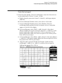
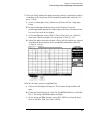
Performance Test Record
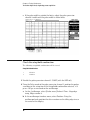
Performance Test Record
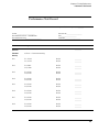
$JLOHQW6HULHV/RJLF$QDO\]HUBBBBBBB
6HULDO1RBBBBBBBBBBBBBBBBBBBBBB
:RUN2UGHU1RBBBBBBBBBBBBBBBBBBB
5HFRPPHQGHG7HVW,QWHUYDO<HDUVKRXUV
'DWHBBBBBBBBBBBBBBBBBBB
5HFRPPHQGHGQH[WWHVWLQJBBBBBBBBBBBBBBBBBBB
7HPSHUDWXUHBBBBBBBBBBBBBBBBBBB
7HVW
6HWWLQJV
5HVXOWV
3DVV)DLO
BBBBBBBB
3DVV)DLO
3DVV)DLO
BBBBBBBB
BBBBBBBB
3DVV)DLO
3DVV)DLO
BBBBBBBB
BBBBBBBB
6HOI7HVWV
7KUHVKROG
$FFXUDF\
±P9RIWKUHVKROGVHWWLQJ
3RG
(&/P9
9P9
3RG
(&/±P9
9±P9
3RG
(&/±P9
9±P9
3DVV)DLO
3DVV)DLO
BBBBBBBB
BBBBBBBB
3RG
(&/±P9
9±P9
3DVV)DLO
3DVV)DLO
BBBBBBBB
BBBBBBBB
3RG
(&/±P9
9±P9
3DVV)DLO
3DVV)DLO
BBBBBBBB
BBBBBBBB
3RG
(&/±P9
9±P9
3DVV)DLO
3DVV)DLO
BBBBBBBB
BBBBBBBB
3RG
(&/±P9
9±P9
3DVV)DLO
3DVV)DLO
BBBBBBBB
BBBBBBBB
3RG
(&/±P9
9±P9
3DVV)DLO
3DVV)DLO
BBBBBBBB
BBBBBBBB
69
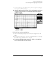
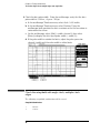
Chapter 3: Testing Performance
Performance Test Record
Performance Test Record (continued)
7HVW
6HWWLQJV
5HVXOWV
3DVV)DLO
6LQJOH&ORFN6LQJOH
(GJH$FTXLVLWLRQ
$OO3RGV&KDQQHO $OO3RGV&KDQQHO
3DVV)DLO
6HWXS+ROG 7LPH
QV
&ON↑
&ON↑
&ON↑
&ON↑
BBBBBBBB
BBBBBBBB
BBBBBBBB
BBBBBBBB
&ON↓
&ON↓
&ON↓
&ON↓
BBBBBBBB
BBBBBBBB
BBBBBBBB
BBBBBBBB
6HWXS+ROG7LPH
QV
&ON↑
&ON↑
&ON↑
&ON↑
BBBBBBBB
BBBBBBBB
BBBBBBBB
BBBBBBBB
&ON↓
&ON↓
&ON↓
&ON↓
BBBBBBBB
BBBBBBBB
BBBBBBBB
BBBBBBBB
6HWXS+ROG 7LPH
QV
&ON↑
&ON↑
&ON↑
&ON↑
BBBBBBBB
BBBBBBBB
BBBBBBBB
BBBBBBBB
&ON↓
&ON↓
&ON↓
&ON↓
BBBBBBBB
BBBBBBBB
BBBBBBBB
BBBBBBBB
6HWXS+ROG 7LPH
QV
&ON↑
&ON↑
&ON↑
&ON↑
BBBBBBBB
BBBBBBBB
BBBBBBBB
BBBBBBBB
&ON↓
&ON↓
&ON↓
&ON↓
BBBBBBBB
BBBBBBBB
BBBBBBBB
BBBBBBBB
6HWXS+ROG7LPH
QV
&ON↑ &ON↑ BBBBBBBB
&ON↑&ON↑
&ON↓&ON↓ &ON↓ &ON↓
BBBBBBBB
6HWXS+ROG7LPH
QV
&ON↑&ON↑
&ON↑&ON↑
BBBBBBBB
&ON↓&ON↓ &ON↓ &ON↓
BBBBBBBB
6HWXS+ROG7LPH
QV
&ON↑ &ON↑ BBBBBBBB
&ON↑&ON↑
&ON↓&ON↓ &ON↓ &ON↓
BBBBBBBB
6HWXS+ROG7LPH
QV
&ON↑ &ON↑ BBBBBBBB
&ON↑&ON↑
&ON↓&ON↓ &ON↓ &ON↓
BBBBBBBB
0XOWLSOH&ORFN
0XOWLSOH(GJH
$FTXLVLWLRQ
3DVV)DLO
$OO3RGV&KDQQHO
$OO3RGV&KDQQHO
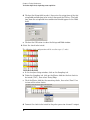
70
3DVV)DLO
Chapter 3: Testing Performance
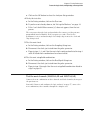
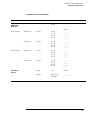
Performance Test Record
Performance Test Record (continued)
7HVW
6HWWLQJV
5HVXOWV
'LVDEOHSXOVHJHQHUDWRUFKDQQHO&203
/('RII
6LQJOH&ORFN
0XOWLSOH(GJH
$FTXLVLWLRQ
3DVV)DLO
$OO3RGV&KDQQHO
$OO3RGV&KDQQHO
7LPH,QWHUYDO
$FFXUDF\
6HWXS+ROG7LPH
QV
&ON↑
↓
&ON↑
↓
&ON↑
↓
&ON↑
↓
BBBBBBB
BBBBBBB
BBBBBBB
BBBBBBB
6HWXS+ROG7LPH
QV
&ON↑
↓
&ON↑
↓
&ON↑
↓
&ON↑
↓
BBBBBBB
BBBBBBB
BBBBBBB
BBBBBBB
6HWXS+ROG7LPH
QV
&ON↑
↓
&ON↑
↓
&ON↑
↓
&ON↑
↓
BBBBBBB
BBBBBBB
BBBBBBB
BBBBBBB
6HWXS+ROG7LPH
QV
&ON↑
↓
&ON↑
↓
&ON↑
↓
&ON↑
↓
BBBBBBB
BBBBBBB
BBBBBBB
BBBBBBB
([SHFWHG
/LPLWV
0HDVXUHG
µV
µVWR
µV
BBBBBBBBB
71
Chapter 3: Testing Performance
Performance Test Record
72
4
Calibrating and Adjusting
This chapter gives you instructions for calibrating and adjusting the logic
analyzer.
73
Chapter 4: Calibrating and Adjusting
Logic analyzer calibration
The logic analyzer circuitry of the Agilent 1680/90-series Logic Analyzers does
not require an operational accuracy calibration. To test the logic analyzer
circuitry against specifications (full calibration), refer to chapter 3, "Testing
Performance."
74
5
Troubleshooting
This chapter helps you troubleshoot the logic analyzer to find defective
assemblies.
75
Chapter 5: Troubleshooting
The troubleshooting consists of flowcharts, self-test instructions, and tests. This
information is not intended for component-level repair.
If you suspect a problem, start at the top of the first flowchart. During the
troubleshooting instructions, the flowcharts will direct you to perform other
tests.
The service strategy for this instrument is the replacement of defective
assemblies. This instrument can be returned to Agilent Technologies for all
service work, including troubleshooting. Contact your nearest Agilent
Technologies Sales Office for more details.
CAUTION:
Electrostatic discharge can damage electronic components. Use grounded wriststraps
and mats when you perform any service to this instrument or to the cards in it.
NOTE:
If any peripheral hardware or software programs were installed by the user into an
Agilent 1680A,AD-series logic analyzer, they must be first uninstalled and removed before
doing any troubleshooting. Removing user-installed hardware or software will rule out the
possibility they are causing problems and/or conflicts in the logic analyzer operating
system or application software. Troubleshooting is best done if the instrument is returned
to its hardware and software factory configuration.
To install the fan guard
Installing the fan guard is recommended for any power-on troubleshooting for
either the Agilent 1680A,AD-series or 1690A,AD-series.
NOTE:
The fan guard protects repair personnel from potential injury caused by rotating fan
blades.
1 Remove the chassis from the sleeve. Follow the procedure “To remove the
chassis from the sleeve” on page 110 .
2 Install the fan guard onto the chassis.
a Position the chassis so the handle side is up.
b Slide the fan guard onto the chassis over the fans.
On an Agilent 1680A,AD-series, a guide hole in the fan guard will slide over the
standoff post of the bottom left rear foot (adjacent to the acquisition board BNC
connectors).
76
Chapter 5: Troubleshooting
c Install the optional screws as shown.
3 After the required power-on troubleshooting and repair is complete,
reverse the above procedure to remove the fan guard and reassemble the
instrument.
To use the flowcharts
Flowcharts are the primary tool used to isolate defective assemblies. The
flowcharts refer to other tests to help isolate the trouble. The circled letters on
the charts indicate connections with the other flowcharts. Start your
troubleshooting at the top of the first flowchart.
77
Chapter 5: Troubleshooting
Troubleshooting the Agilent 1680A,AD-series
Troubleshooting the Agilent 1680A,AD-series
START
Apply power and
observe the
instrument front
panel.
Did the front
panel indicators
flash?
No
2
Yes
Are all
instrument power
supply fans
running?
No
3
Yes
Does the
display light
up?
Yes
Does the
instrument finish
booting?
No
No
4
5
Yes
Launch the Agilent
Logic Analyzer
application
software.
Does the
application
software launch?
No
6A
Yes
Is the
application
Online?
No
6B
Yes
Do the self test.
Refer in Chapter 5.
Do the self
tests pass?
Replace the
acquisition
board.
No
Yes
Is the problem
still present?
Yes
01680b05
7
No
DONE
78
Chapter 5: Troubleshooting
Troubleshooting the Agilent 1680A,AD-series
2
Are the power
supply fans
running?
No
Ensure the power cord is
properly connected.
Yes
Are the instrument
fans running?
No
Is the power cord
connected?
Suspect the power supply. Do
the procedure To test the
power supply voltages in
Chapter 5.
Remove the cover and
ensure all front panel cables
are properly connected.
Yes
Do all test points
pass?
No
Reconnect the front
panel cables.
Reconnect the
power cord.
Yes
Yes
Are all cables
connected?
No
No
Yes
Replace the front panel
circuit board.
Ensure all instrument cables
are connected and properly
seated.
Replace the
power supply.
01680b06
1
79
Chapter 5: Troubleshooting
Troubleshooting the Agilent 1680A,AD-series
3
Are the power
supply fans
running?
No
Yes
Are both instrument
fans stopped?
Yes
No
Verify the fan voltage.
Do the procedure To test
the fan voltage in Chapter 5.
Are the fan voltages
OK?
No
Suspect the power supply.
Do the procedure To test the
power supply voltages in
Chapter 5.
Yes
Do all test points pass?
No
Yes
Replace the defective fan.
Replace the
distribution board.
Replace the
power supply.
1
80
01680b07
Chapter 5: Troubleshooting
Troubleshooting the Agilent 1680A,AD-series
4
Connect an external
800x600 PCmonitor to
the instrument.
Does the external
monitor light up
No
Yes
Is the external
monitor readable?
No
Possible problemwith
motherboard or PCI
video board
Ensure PCI video board is
seated in the motherboard
connector.
Yes
Possible problemwith
LCDdisplay, inverter,
or cables.
Is the PCI video
board seated in the
motherboard?
No
Reseat the PCI video
board in the
motherboard connector.
Yes
Replace PCI video
board with known
good board.
Reconnect an external
800x600 PCmonitor to
the instrument.
Are all cables
connected and
seated?
Yes
Is the external
monitor readable?
Yes
No
Reconnect or reseat all
video cabling.
No
Replace the LCD
display and inverter.
Replace defective PCI
video board.
Replace motherboard.
01680b08
1
81
Chapter 5: Troubleshooting
Troubleshooting the Agilent 1680A,AD-series
5
Yes
Does the blue Agilent
Logic Analyzer screen
appear?
No
Replace the CPU
motherboard.
Yes
No
Does an *error
message appear
during POST?
Does the
instrument boot
any further?
Yes
Remove power from
the instrument,
remove the cover and
check all cables are
properly seated.
Reapply power,
observe if any error
messages appear.
No
Does an *error
message appear?
* Microsoft Windows 2000 Resource Kits include and error message
reference that will help identify the cause of specific error messages.
The Microsoft Windows 2000 Resource Kits are currently at URL:
http://www.microsoft.com/windows2000/techinfo/reskit/en/default.asp
No
Yes
Does the *error
message refer to the
hard disk drive?
No
Address the specific
message as a
hardware failure.
Yes
Does an *error
message appear
regarding Master
Boot Record?
Replace the
hard disk
drive.
Yes
Replace failed
hardware as
indicated in the
error message.
No
Does
" Starting Windows...
appear?
No
"
Yes
Does the operating
system logon screen
appear?
No
Is logon
disabled?
No
Reinstall operating
system. Refer to the
procedure To recover
the operating system.
01680b09
Yes
Yes
1
82
Chapter 5: Troubleshooting
Troubleshooting the Agilent 1680A,AD-series
6A
Uninstall, then reinstall
the Agilent Logic
Analyzer application.
Does the
application
software launch?
No
Yes
Do error
messages appear?
Yes
Do the procedure To
recover the operating
systemin Chapter 5.
No
1
6B
Remove power fromthe
instrument. Remove the cover
and check the internal IEEE
1394 cabling.
Are all cables
connected and
seated?
No
Reconnect or reseat all
internal cabling.
Yes
Reseat the PCI IEEE
board in ISA slot 1*.
Apply power to the
instrument.
Is the application
Online?
* All PCI boards must be installed
in the correct slots. Refer to the
procedure To remove the ISA
board in Chapter 6.
No
Observe the status LEDs
on the acquisition board.
Refer to Acquisition board
status LEDs.
Yes
Are any green
LEDs blinking?
Yes
No
Possible problemwith PCI
IEEE 1394 board. Replace
the PCI IEEE 1394 board.
Possible problemwith
acquisition board. Replace
the acquisition board.
01680b10
1
83
Chapter 5: Troubleshooting
Troubleshooting the Agilent 1680A,AD-series
7
Possible problem with logic
analyzer cables. Do the
cable test in Chapter 5 on
suspect pod.
Does cable test
pass?
Yes
The logic analyzer
board is functioning
properly.
No
Swap suspect probe tip
assembly with known
good one.
Does cable test
pass?
Yes
Replace defective
probe tip assembly.
Yes
Replace defective
cable.
No
Swap suspect cable
assembly with known
good one.
Does cable test
pass?
No
Replace logic analyzer
acquisition board.
01680b11
1
84
Chapter 5: Troubleshooting
Troubleshooting the Agilent 1680A,AD-series
To check the power-up tests
The power-up self tests on the 1680A,AD-series logic analyzers is performed by
the Microsoft Windows 2000 Professional operating system. As part of the
Windows 2000 Professional power on self test (POST), the presence of all
required system components is verified.
1 Close the Agilent Logic Analyzer application and all other applications
running on the logic analyzer.
2 Shut down the instrument.
a Click on the Start button in the task bar, then select Shut Down.
b In the Shut Down window, select Shut Down from the menu, then
select the OK button.
c After the instrument turns off, press the power button to again apply
power.
Monitor the boot dialogue. When the text "Starting Windows . . ." appears at the
bottom of the screen, this means required system components have been
detected and have passed their power-up self-tests.
To test the power supply voltages
Refer to chapter 6, "Replacing Assemblies," for instructions to remove or replace
covers and assemblies.
This procedure will not expose any problems related to load regulation; however,
it will show most failure modes to over 95% confidence,
WARNING:
Hazardous voltages exist on the power supply. This procedure is to be
performed by service-trained personnel aware of the hazards involved, such as
fire and electrical shock.
1 Close the Agilent Logic Analyzer application and all other applications
running on the logic analyzer.
2 Shut down the instrument.
a Click on the Start button in the task bar, then select Shut Down.
b In the Shut Down window, select Shut Down from the menu, then
select the OK button.
85
Chapter 5: Troubleshooting
Troubleshooting the Agilent 1680A,AD-series
3 Remove the power supply from the instrument. Refer to “To remove the
power supply” in Chapter 6.
4 After removing the power supply, connect a power cord to the power
supply and plug the power cord into line power.
5 Using DVM, measure the power supply voltages.
Power Supply Voltages
&1
&1
3LQ
9ROWDJH
3LQ
9ROWDJH
1-5
+3.3 V
1-4
-5.2 V
6-7
COM
5
+12 V
8-10
+5 V
6-8
-12 V
11-12
COM
9-12
COM
13-14
+3.3 V
13
+12 V
15-19
COM
14-16
COM
20-21
+5 V
22-24
COM
6 Note problems with the power supply, then unplug the power supply from
line power. Return to the flow chart.
86
Chapter 5: Troubleshooting
Troubleshooting the Agilent 1680A,AD-series
To test the LCD display signals
Before attempting to do this procedure, ensure that the video signal cable
connected to the PCI video board is properly seated. Attempt to reseat the cable
two or three times. If other repairs were done to the instrument, and the video is
now no longer operating, it is very likely that the video cable is not properly
seated.
Refer to chapter 6, "Replacing Assemblies", for instructions to remove or replace
covers and assemblies.
WARNING:
Warning Hazardous voltages exist on the power supply and the LCD display,
and the LCD inverter. This procedure is to be performed by service-trained
personnel aware of the hazards involved, such as fire and electric shock.
1 Remove the sleeve. Refer to chapter 6 for more information on how to
remove the sleeve.
2 Connect a power cord to the instrument and apply power.
3 Using an oscilloscope, probe the following pins of J111 for digital signals.
2, 4, 5
9, 10, 11, 13, 14, 15
29, 30, 31, 33, 34, 35, 37
IFGU
87
Chapter 5: Troubleshooting
Troubleshooting the Agilent 1680A,AD-series
4 Using an oscilloscope, probe pins 39 and 40 of J111 for +3.3Vdc
If +3.3Vdc is present on J111 of pins 39 and 40, and digital signals are present on
the video data pins indicated above, then the CPU board video circuit is operating
properly.
5 Remove power. Allow time for the capacitors in the power supply to
discharge before disconnecting the power supply, doing the repair, and
reassembling the instrument.
To test disk drive voltages
The following procedure is a guide to help further identify possible problems with
either the flexible disk drive or hard disk drive.
Equipment Required
(TXLSPHQW
&ULWLFDO6SHFLILFDWLRQ
5HFRPPHQGHG0RGHO3DUW
'LJLWL]LQJ2VFLOORVFRSH
!0+]%DQGZLGWK
%
1 Close the Agilent Logic Analyzer application and all other applications
running on the logic analyzer.
2 Shut down the instrument.
a Click on the Start button in the task bar, then select Shut Down.
b In the Shut Down window, select Shut Down from the menu, then
select the OK button.
3 After the instrument turns off, unplug the instrument and remove the
cover.
4 Disconnect the suspect disk drive. Remove the disk drive from the chassis
and reconnect the cable.
5 Troubleshoot a hard disk drive.
a Apply power to the instrument.
88
Chapter 5: Troubleshooting
Troubleshooting the Agilent 1680A,AD-series
b As the instrument is booting, probe for digital signals on the hard disk
drive connector according to the following table.
Disk Drive Voltages
3LQ1R
6LJQDO
9ROWDJH
3LQ1R
6LJQDO
9ROWDJH
3LQ1R
6LJQDO
5(6(7
'$7$
,25'<
3',$*
&6(/
'$
.(<
'0$&.
'$
'0$54
,1754
&6
',2:
,2&6
&6
',25
'$
'$63
9ROWDJH
3LQVDUH*5281'
3LQVDQGDUH9GF
6 Troubleshoot a flexible disk drive.
a Apply power to the instrument.
b After the instrument finished booting, launch the Agilent Logic
Analyzer application.
c Insert a formatted flexible disk in the instrument flexible disk drive.
d Attempt to do a File Save of the Agilent Logic Analyzer default
configuration to the flexible disk drive.
89
Chapter 5: Troubleshooting
Troubleshooting the Agilent 1680A,AD-series
e While the instrument is attempting to save the file to flexible disk,
probe for digital signals on the flexible disk drive connector according
to the following table.
Disk Drive Voltages
3LQ
6LJQDOV
3LQ1R
6LJQDO
9
,1'(;
9
'5,9(6(/(&7
9
',6.&+$1*(
1&
5($'<
1&
0272521
1&
',5(&7,216(/(&7
1&
67(3
9
:5,7('$7$
9
:5,7(*$7(
9
75$&.
29
:5,7(3527(&7
9
5($''$7$
9
6,'(21(6(/(&7
7 Repeat steps 1 through 3 above. After the instrument turns off, unplug the
instrument.
8 Replace suspect disk drive if necessary, then reassemble the instrument.
To verify the CD-ROM
The CD-ROM drive itself can be tested using an audio CD. Install CD player-style
headphones in the CD-ROM audio output jack. With the instrument powered on,
insert an audio CD into the CD-ROM drive. If the CD-ROM is operating properly,
it should begin playing the audio CD.
90
Chapter 5: Troubleshooting
Troubleshooting the Agilent 1680A,AD-series
To recover the operating system
To reinstall the operating system
Reinstalling the operating system erases the entire hard disk drive and
reinitializes the hard disk drive to its factory configuration. All user data stored
on the hard disk drive will be lost. Reinstalling the operating system is necessary
in case any system level files or other components of the operating system
become corrupted.
The recovery CD-ROM does not contain an image of the Windows 2000
Professional operating system. An image of the operating system resides on a
hidden area of the hard disk drive. The CD-ROM contains an install key which
recognizes whether or not the system motherboard is an Agilent logic analyzer
motherboard. If the system motherboard is an Agilent logic analyzer
motherboard, then the install key permits the recovery of the operating system
from the hidden area of the hard disk drive.
1 Apply power to the instrument.
2 After applying power, insert the recovery CD-ROM in the instrument CDROM drive.
If the instrument finishes booting, then user files can likely be archived so they
don’t become lost.
3 Press the on/off button to turn the instrument off.
4 After a few seconds turn the instrument back on.
5 At the prompt, select "Yes" to reinstall the operating system.
It takes about 1 hour to reinstall the operating system and Agilent Logic Analyzer
application software. At the end of the operating system reinstallation, the logic
analyzer will be in its factory default operating system configuration.
Problems running the Application Software
If there is a problem while running the Agilent Logic Analyzer application
software, then the likely cause would be the application if the error or unusual
behavior appeared while configuring a window or analyzing data.
In the event of a problem of the Agilent Logic Analyzer application software, do
the following steps:
In case the application software becomes unresponsive, do a Ctrl-Alt-Del and follow
the queries to abort the application software. Attempt to restart the application
software and do a measurement.
91
Chapter 5: Troubleshooting
Troubleshooting the Agilent 1680A,AD-series
If there are still problems running the application software, then uninstall and reinstall
the application software.
Problems with the Operating System
Operating system applies to the Agilent 1680A,AD-series logic analyzers. The
likely cause would be the operating system if the error or unusual behavior
appeared while doing an operating system task, like printing or configuring the
network.
In the event of a problem with the operating system, do the following steps:
If error messages appear, consult the operating system documentation for information
related to the errors.
In case the whole system becomes unresponsive, turn the instrument off by pressing
the on/off button. If pressing the on/off button does not initiate the power-down
routine, then press and hold the on/off button for 5 seconds until the instrument turns
off.
Turn on the instrument and reattempt the task. If the whole system again becomes
responsive then follow the above procedure To reinstall the operating system.
For a host PC controlling an Agilent 1690A,AD-series hosted logic analyzer,
responsibility of diagnosing errors and problems with utilized system services is
the user’s.
92
Chapter 5: Troubleshooting
Troubleshooting the Agilent 1690A,AD-series
Troubleshooting the Agilent 1690A,AD-series
START
Apply power
Are all
instrument and
power supply
fans running.
No
2
Yes
Launch the Agilent Logic
Analyzer application
software on the host PC.
Does the application
software launch?
No
3A
Yes
Is the application
Online?
No
3B
Yes
Do the self test. Refer to
Chapter 5.
Do the self
tests pass?
No
Replace the
acquisition board.
Yes
Is the problem
still present?
Yes
4
01690b01
No
DONE
93
Chapter 5: Troubleshooting
Troubleshooting the Agilent 1690A,AD-series
2
Are the power
supply fans running?
No
Ensure the power cord is
properly connected.
Yes
Is the power cord
connected?
No
Reconnect the power
cord.
Yes
Are the instrument
fans running?
No
Suspect the power
supply. Do the power
supply voltages check in
Chapter 5.
Yes
Do all test points pass?
No
Yes
Ensure all instrument
cables are connected and
properly seated.
Replace the power
supply.
1
94
01690b02
Chapter 5: Troubleshooting
Troubleshooting the Agilent 1690A,AD-series
3A
Uninstall, then reinstall
the Agilent Logic
Analyzer application.
Does the
application
software launch?
No
Yes
Do error messages
appear?
Yes
Possible problem with host
operating system. Consult
host PC documentation.
No
1
3B
Is the IEEE 1394
cable connected and
seated?
No
Reconnect or reseat IEEE
1394 cable.
No
Uninstall, then reinstall the
Agilent Logic Analyzer
application.
Yes
Do the procedure To
verify connectivity in
Chapter 5.
Is connectivity
verified?
Yes
Remove the cover and
observe the status LEDs
on the acquisition board.
Are any green
LEDs blinking.
Yes
No
Possible problem with
PCI IEEE 1394 board on
host PC. Replace the
board.
Possible problem with
acquisition board. Replace
the acquisition board.
01690b03
1
95
Chapter 5: Troubleshooting
Troubleshooting the Agilent 1690A,AD-series
4
Possible problem with
logic analyzer cables. Do
the cable test in chapter 5
of suspect pod.
Does cable test
pass?
Yes
The logic analyzer board
is functioning properly.
Yes
Replace defective
probe tip assembly.
Yes
Replace defective
cable.
No
Swap suspect probe tip
assembly with known
good one.
Does cable test
pass?
No
Swap suspect cable
assembly with known
good one.
Does cable test
pass?
No
Replace logic analyzer
acquisition board.
01690b04
1
96
Chapter 5: Troubleshooting
Troubleshooting the Agilent 1690A,AD-series
To verify connectivity
Using Windows Device Manager and Task Manager, you can quickly determine if
the Agilent Logic Analyzer application software is correctly installed on a host
PC.
Task Manager
Use Task Manager to see if the ag1680svc is running. The ag1680svc is started
when the PC is booted and establishes connection with the 1690A,AD-series
hosted logic analyzer when the logic analyzer is connected to the PC. If the
ag1680svc service is not listed, then the host PC will not be able to establish an
interface with the hosted logic analyzer.
If the ag1680svc service is not listed, then uninstall and reinstall the Agilent Logic
Analyzer application software. If the ag1680svc service still does not appear, then
there is a problem with your Windows 2000 Professional operating system.
Consult the documentation for the operating system to further determine why
the service is not being installed and run.
97
Chapter 5: Troubleshooting
Troubleshooting the Agilent 1690A,AD-series
Device Manager
Use Device Manager to see if the Agilent Logic Analyzer device has been properly
installed. The Device Manager should include an entry "Logic Analyzers" with the
device "Agilent Technologies 1680 Series Analyzer".
If the logic analyzer device is not listed, then uninstall and reinstall the Agilent
Logic Analyzer application software. If the device still does not appear, then there
is a problem with the Windows 2000 Professional operating system. Consult the
documentation for the operating system to determine why the device is not being
installed and run.
To test the power supply voltages
Refer to chapter 6, "Replacing Assemblies," for instructions to remove or replace
covers and assemblies.
This procedure will not expose any problems related to load regulation; however,
it will show most failure modes to over 95% confidence,
WARNING:
Hazardous voltages exist on the power supply. This procedure is to be
performed by service-trained personnel aware of the hazards involved, such as
fire and electrical shock.
1 Close the Agilent Logic Analyzer application and all other applications
running on the logic analyzer.
2 Shut down the instrument.
a Click on the Start button in the task bar, then select Shut Down.
b In the Shut Down window, select Shut Down from the menu, then
select the OK button.
98
Chapter 5: Troubleshooting
Troubleshooting the Agilent 1690A,AD-series
3 Remove the power supply from the instrument. Refer to “To remove the
power supply” in Chapter 6.
4 After removing the poser supply, connect a power cord to the power
supply and plug the power cord into line power.
5 Using DVM, measure the power supply voltages.
Power Supply Voltages
&1
&1
3LQ
9ROWDJH
3LQ
9ROWDJH
1-3
+3.4 V
1,2
+5.1 V
4,5
COM
3
COM
6,7
+3.4 V
4
-5.2 V
8-10
COM
5,6
COM
7
+12 V
8
+5.1 V
9,10
COM
11,12
-5.2 V
13
COM
14
+12 V
6 Note problems with the power supply, then unplug the power supply from
line power. Return to flow chart.
99
Chapter 5: Troubleshooting
General Troubleshooting
General Troubleshooting
This section includes troubleshooting procedures that can be done on either the
Agilent 1680A,AD- or 1690A,AD-series logic analyzers. Before any of these
procedures can be done on an Agilent 1690A,AD-series logic analyzer, the logic
analyzer must be connected to a host PC and both the host PC and the logic
analyzer must be turned on.
To run the self-tests
The self-tests verify the operation of the logic analyzer acquisition system. Selftests can be performed all at once or one at a time. More information about the
logic analyzer self-tests can be found in Chapter 8.
1 Do the following steps for an Agilent 1690A,AD-series:
a Connect the logic analyzer to a host PC and apply power.
b Apply power to the host PC and allow the PC to finish booting.
2 For an Agilent 1680A,AD-series logic analyzer, apply power to the
instrument and allow it to finish booting.
3 Launch the Agilent Logic Analyzer application. When the application
launches, observe the status field and ensure it reads “Online.”
4 In the Agilent Logic Analyzer application window, click on Help. At the
pop-up window, click on Self Test, then select Analyzer Self Test. The
Logic Analyzer Self Test window will appear.
100
Chapter 5: Troubleshooting
General Troubleshooting
5 In the Logic Analyzer Self Test window, click on the Run All Tests button.
The pass/fail status of each test is reported as the test completes. When all self
tests are complete, a summary is printed in the status window concluding with
“ALL Tests PASSED” or with failure information.
The self tests can be run one at a time by clicking on the self-test of interest. The
results of the individual test will be reported under Test Results. For example, if
you select the Memory Test the following results should be reported in the status
window:
101
Chapter 5: Troubleshooting
General Troubleshooting
Acquisition board status LEDs
The acquisition board has four LEDs located close to its IEEE 1394 port. The
LEDs report the status of configuration of both the interface field programmable
gate array (FPGA) and the IEEE 1394 link layer on the acquisition board.
Green LEDs
The green LEDs display the status of loading of the IEEE 1394 link layer.
When the IEEE 1394 is successfully loaded, the system processor on the CPU
Motherboard can communicate with the acquisition board. The system processor
can then configure and download information from the acquisition board.
Red LED
The Red LED shows the status of the configuration software load of the interface
FPGA in the acquisition board.
When the Red LED is on and steady, this indicates the FPGA configuration
software has not been successfully loaded into the FPGA. Failure to load the
FPGA configuration can be caused by either a failure of the acquisition board or a
failure of the PCI IEEE 1394 board. Failure to load the FPGA configuration can
also be caused by a missing or misconfigured ag1680svc service.
Normal Operation
During normal operation, the red LED is off and all three green LEDs are
illuminated.
During power up (1680A,AD-series) or connection (1690A,AD-series), the green
LEDs first blink on then off. The acquisition board processor attempts to initialize
and load the IEEE 1394 link layer. The individual status LEDs represent the
success or failure of three steps needed to initalize, load, and then run the IEEE
1394 link layer. When each of the green LEDs illuminate:
102
Chapter 5: Troubleshooting
General Troubleshooting
LED #1 (closest to the red LED) - the on-board processor is properly initialized and
running, attempting to load the IEEE 1394 link layer configuration
LED #2 - the IEEE 1394 link layer is loaded and configured
LED #3 - the IEEE 1394 is loaded, properly configured, and is running
A blinking green LED signifies a failure of one of the above steps. In this case, the
acquisition board must be replaced.
When the IEEE 1394 port on the acquisition board is configured and initialized,
the ag1680svc service running on the Windows 2000 Professional operating
system senses the acquisition board. The ag1680svc service then loads
configuration code into the interface FPGA on the acquisition board. When the
FPGA is configured, the red LED is turned off. The acquisition board is then
properly configured and initialized both to communicate with the system
processor and to acquire data.
To test the logic analyzer probe cables
This test allows you to functionally verify the probe cable and probe tip assembly
of any of the logic analyzer pods. Only one probe cable can be tested at a time.
Repeat this test for each probe cable to be tested.
Equipment Required
5HFRPPHQGHG
0RGHO3DUW
(TXLSPHQW
&ULWLFDO6SHFLILFDWLRQ
3XOVH*HQHUDWRU
0+]QVSXOVHZLGWK
SVULVHWLPH
$2SWLRQ
$GDSWHU4W\
60$P%1&I
&RXSOHU4W\
%1&PP
[7HVW&RQQHFWRUV4W\
1 Turn on the equipment and the logic analyzer.
103
Chapter 5: Troubleshooting
General Troubleshooting
2 Set up the pulse generator according to the following table.
Pulse Generator Setup
7LPHEDVH
&KDQQHO
7ULJJHU
&KDQQHO
0RGH,QW
0RGH3XOVH
'LYLGH'LYLGH
0RGH6TXDUH
3HULRGQV
'LYLGH6TXDUH÷ $PSO9
'HOD\QV
2IIV9
$PSO9
$PSO9
2IIV9
2IIV9
&203'LVDEOHG/('2II
&203'LVDEOHG/('2II
3 Using four 6-by-2 test connectors, four BNC Couplers, and four SMA (m) BNC (f) Adapters, connect the logic analyzer to the pulse generator
channel outputs. To make the test connectors, see chapter 3, "Testing
Performance."
a Connect the even-numbered channels of the lower byte of the pod
under test and Clk 1 to the pulse generator channel 1 OUTPUT.
b Connect the odd-numbered channels of the lower byte of the pod under
test to the pulse generator channel 1 OUTPUT.
c Connect the even-numbered channels of the upper byte of the pod
under test to the pulse generator channel 2 OUTPUT.
d Connect the odd-numbered channels of the upper byte of the pod
under test to the pulse generator channel 2 OUTPUT.
4 Configure the Analyzer Setup window.
a In the Waveform window, click on the Sampling Setup icon.
b In the Analyzer Setup window under the Sampling tab, click on State Synchronous Sampling to select.
c Under the Sampling tab, configure Trigger Position - 100% poststore.
d Click on the Acquisition Depth field, then select 8K.
104
Chapter 5: Troubleshooting
General Troubleshooting
e Under the Sampling tab, click on the Master field for the clock to be
tested, then select Either Edge.
5 Configure the pod under test.
a In the Analyzer Setup window, click on the Buses/Signals tab
b Click on the Delete All button at the bottom of the window.
c Using the mouse, activate all channels for the pod under test. The
channels will be assigned to label My Bus 1.
d Click on the threshold field for the pod under test. the Threshold
Settings window will appear.
e In the Threshold Settings window, click on the threshold field, then in
the pop-up menu select ECL (-1.30 V).
f In the Threshold Settings window, click OK to close the window.
g In the Analyzer Setup window, click OK to close the window.
6 Verify the data.
a Click on the Listing - Listing 1 tab.
105
Chapter 5: Troubleshooting
General Troubleshooting
b In the Listing window, click on the Run icon. The display should look
similar to the figure below.
7 Repeat steps 3 through 7 to test other logic analyzer cables.
8 Disconnect the test equipment from the logic analyzer.
9 If the display looks like the figure, then the cable passed the test.
If the display does not look similar to the figure, then there is a possible problem
with the cable or probe tip assembly. Causes for cable test failures include the
following:
•
open channel
•
channel shortened to a neighboring channel
•
channel shortened to either ground or a supply voltage
Return to Troubleshooting flowchart 7.
To check the BNC Trigger input/output signals
1 Turn on the equipment and the logic analyzer.
2 Set up the DC source to deliver a DC voltage on the output.
a In the function generator Utility menu, activate the DC Level. All AC
voltage functions will be disabled.
b Enable the high impedance load under the Output Setup menu.
3 Connect the equipment to the logic analyzer.
a On the DC source, enter a voltage setting of 0.000 V.
b Using a BNC cable, connect the output of the DC Source to the logic
analyzer Trigger In BNC.
106
Chapter 5: Troubleshooting
General Troubleshooting
c Using a BNC-banana cable, connect the voltmeter to the logic analyzer
Trigger Out BNC.
The voltmeter will display a voltage approximately 3 Vdc.
4 Configure the external trigger.
a In the logic analyzer Waveform window, select the Trigger Setup icon.
b In the Trigger window under Trigger Sequence Step 1, select Anything.
c At the pop-up menu, select Arm in from Ext. Trigger.
d In the Trigger window, click OK to close the window.
5 Verify the external trigger.
a In the logic analyzer Waveform window, select the Run icon.
The logic analyzer will report "Waiting in Trigger Step 1...". The voltmeter will
display approximately 0 Vdc.
b On the DC source, enter a voltage setting of 3.000 V
The voltmeter will display approximately 3 Vdc. The logic analyzer will trigger
and display a waveform similar to the following:
c On the DC source, re-enter the voltage setting of 0.000 V
6 Disconnect the test equipment from the logic analyzer.
107
Chapter 5: Troubleshooting
General Troubleshooting
To test the auxiliary power
The +5 V auxiliary power is protected by a current overload protection device. If
the current on pins 1 and 39 exceed 0.33 amps, the circuit will open. When the
short is removed, the circuit will reset in approximately 1 minute. There should
be +5 V after the 1 minute reset time.
Equipment Required
5HFRPPHQGHG
0RGHO3DUW
(TXLSPHQW
&ULWLFDO6SHFLILFDWLRQV
'LJLWDO0XOWLPHWHU
P9UHVROXWLRQEHWWHUWKDQ ($
DFFXUDF\
• Use the multimeter to verify the +5 V on pins 1 and 39 of the probe cables.
108
6
Replacing Assemblies
This chapter contains the instructions for removing and replacing the assemblies
of the logic analyzer. Also in this chapter are instructions for returning
assemblies.
109
Chapter 6: Replacing Assemblies
1680A,AD-series disassembly/assembly
1680A,AD-series disassembly/assembly
Prepare the instrument for disassembly
Do this procedure before doing any disassembly procedure on the instrument.
1 Close the Agilent Logic Analyzer application software.
2 Gracefully shut down the operating system and remove power when
shutdown is complete.
3 Remove the power cord.
4 Move the instrument to a static safe work environment.
To remove the chassis from the sleeve
Before disassembling the instrument, it must be turned off and placed in a static
safe work environment. If you haven’t already done so, do the previous procedure
"Prepare the instrument for disassembly."
1 Using a Torx T-15 screwdriver, remove the two screws that secure the
handle to the side of the instrument and lift off the handle.
2 Using a Torx T-10 screwdriver, remove five screws that secure the logic
analyzer cables to the rear panel of the logic analyzer.
3 Disconnect the logic analyzer cables from the rear panel. Remove the logic
analyzer cables (and spacers, if installed) from the logic analyzer.
4 Using a Torx T-15 screwdriver, remove the screws connecting the four rear
feet to the instrument, one screw per foot. Remove each foot from the rear
panel.
5 Using a Torx T-10 screwdriver, remove eleven screws that secure the
sleeve to the chassis.
6 With the logic analyzer upright, slide the chassis out of the sleeve.
110
Chapter 6: Replacing Assemblies
1680A,AD-series disassembly/assembly
7 Reverse this procedure to install the chassis into the sleeve.
When reassembling, check the following:
all assemblies are properly installed before installing the chassis into the sleeve.
ensure all exposed cables are dressed properly so the sleeve does not cause any
damage to the cables.
To remove the acquisition board
1 Do the procedure "To remove the chassis from the sleeve".
2 Turn the chassis upside down.
3 Disconnect the IEEE 1394 cable from the acquisition board.
4 Using a Torx T-10 screwdriver, remove five screws that secure the probe
shroud to the rear panel of the logic analyzer.
5 Using a Torx T-10 screwdriver, remove one screw that secures the
acquisition board to the chassis (center of the acquisition board).
111
Chapter 6: Replacing Assemblies
1680A,AD-series disassembly/assembly
6 Slide the acquisition board out the rear panel of the logic analyzer.
Steps to remove probe shroud from acquisition board.
7 Using a hex screwdriver, remove two hex nuts from the acquisition board
trigger BNC connectors.
8 Using a Torx T-10 screwdriver, remove five screws that secure the probe
shroud to the acquisition board.
Reverse this procedure to install the acquisition board.
If the probe shroud requires replacing, then the probe shroud label (part number
01680-94312) must also be ordered and installed on the replacement probe
shroud.
112
Chapter 6: Replacing Assemblies
1680A,AD-series disassembly/assembly
To remove the power supply
1 Do the procedure "To remove the chassis from the sleeve".
2 Disconnect the 16-pin power supply cable and the power sense cable from
the distribution board.
3 Using a Torx T-15 screwdriver, remove four screws that secure the power
supply to the chassis.
4 Lift the power supply out of the chassis.
5 Disconnect the 14-pin and the 10-pin power supply cables from the
distribution board.
113
Chapter 6: Replacing Assemblies
1680A,AD-series disassembly/assembly
6 Reverse this procedure to install the power supply
When installing a replacement power supply, transfer the power supply cables
and the grommet to the replacement power supply as shown:
To remove the hard disk drive
1 Do the procedure "To remove the chassis from the sleeve".
2 Using a Torx T-15 screwdriver, remove four screws that secure the hard
disk drive to the chassis.
3 Lift the hard disk drive out of the chassis.
4 Disconnect both the power cable and the data cable from the hard disk
drive.
5 Reverse this procedure to install the hard disk drive.
114
Chapter 6: Replacing Assemblies
1680A,AD-series disassembly/assembly
To remove the CD-ROM drive
1 Do the procedure "To remove the chassis from the sleeve".
2 Disconnect the IEEE 1394 cable from the PCI IEEE 1394 interface board.
Disengage the cable from the cable clamps on the top of the CD-ROM drive
assembly.
3 Remove the data cable, power cable and audio cable from the CD-ROM
drive interface board.
4 Using a Torx T-10 screwdriver, remove five screws that secure the CDROM drive assembly to the chassis.
5 Slide the CD-ROM assembly out of the chassis.
Perform the following steps to remove the CD-ROM drive from the CDROM assembly.
1 1 Using a Torx T-10 screwdriver, remove two screws that secure the CDROM interface board to the CD-ROM drive brackets.
2 Remove the interface board from the CD-ROM drive brackets.
A connector on the back of the CD-ROM interface board will disengage from an
interface connector on the rear of the CD-ROM drive.
3 Using a Torx T-10 screwdriver, remove two screws, one on each side of the
CD-ROM drive brackets, that secure the top bracket to the bottom
bracket. Separate the two brackets.
115
Chapter 6: Replacing Assemblies
1680A,AD-series disassembly/assembly
4 Using a Torx T-6 screwdriver, remove three screws that secure the CDROM drive to the bottom bracket. Lift the CD-ROM drive out of the bottom
bracket.
Reverse this procedure to reassemble and install the CD-ROM drive. Ensure the
motherboard is properly installed before installing the CD-ROM drive.
To remove the flexible disk drive
1 Do the procedure "To remove the chassis from the sleeve".
2 Unplug the flexible disk drive cable from the rear of the flexible disk drive.
3 Using a Torx T-8 screwdriver, remove two screws that secure the flexible
disk drive to the chassis.
116
Chapter 6: Replacing Assemblies
1680A,AD-series disassembly/assembly
4 Slide the flexible disk drive out the rear of the front panel and out of the
chassis.
5 Reverse this procedure to install the flexible disk drive.
When installing a new flexible disk drive, industrial double-sided tape (Agilent
0460-2010 or similar) is required to dress the cable onto the flexible disk drive.
Apply the tape as shown.
117
Chapter 6: Replacing Assemblies
1680A,AD-series disassembly/assembly
To remove the PCI boards
The following PCI boards are installed on the logic analyzer motherboard:
PCI IEEE 1394 board (slot 1, closest to the CD-ROM drive)
PCI 10/100 LAN board (slot 2)
PCI display board (slot 4)
slot covers (slot 3 and slot 5)
1 Do the procedure "To remove the chassis from the sleeve".
2 Disconnect the cable from the board to be removed:
PCI IEEE 1394 board: IEEE 1394 cable
PCI 10/100 LAN board: none
PCI display board: video cable
3 Using a Torx T-10 screwdriver, remove one screw that secures each PCI
board to the rear panel.
4 Slide each board out the top of the chassis.
If the PCI display board is replaced, check to see if tape is covering the video
cable connector on the board. If tape covers the connector, remove the tape
before installing the PCI display board onto the motherboard.
Reverse this procedure to install the JPCI boards.
118
Chapter 6: Replacing Assemblies
1680A,AD-series disassembly/assembly
To remove the motherboard
1 Do the procedure "To remove the chassis from the sleeve".
2 Do the procedure "To remove the CD-ROM drive" to remove the CD-ROM
assembly from the chassis.
3 Remove all three PCI peripheral boards from the motherboard using the
procedure "To remove the PCI boards."
4 Disconnect the following cables from the motherboard:
power switch cable from motherboard J1 pins 6 and 8
disk drive cable from connector FDD1
power cable from connector CN1, unwrap CPU fan cable from around it
audio cable from connector CD
5 Using a Torx T-10 screwdriver, remove three screws that secure the
motherboard back plate to the rear panel.
119
Chapter 6: Replacing Assemblies
1680A,AD-series disassembly/assembly
6 Using a Torx T-10 screwdriver, remove seven screws that secure the
motherboard to the chassis.
Reverse this procedure to install the motherboard.
If the motherboard requires replacing, then do the following steps:
Transfer the I/O panel to the replacement board
If the I/O board requires replacing, then follow the instructions on page 122 to
install EMI gasket on the replacement I/O panel.120
1 Using a 3/16 inch hex nut driver, remove eight hex standoffs that secure
the I/O panel to the parallel port, VGA port, COM1 port, and COM2 port.
2 Remove the I/O panel from the motherboard.
3 Install the I/O panel onto the replacement motherboard.
120
Chapter 6: Replacing Assemblies
1680A,AD-series disassembly/assembly
4 Install eight hex standoffs onto the motherboard ports and tighten.
Transfer system RAM to the replacement board.
1 Push the locking tabs on the RAM connector outboard to release the RAM
module and disengage it from the connector.
2 Lift the RAM module off of the motherboard.
3 Install the RAM module onto the replacement motherboard connector
DIMM1 with the guide slot towards the power connector.
4 Push the RAM module straight down into the connector until the board is
seated in the connector and the locking tabs engage.
121
Chapter 6: Replacing Assemblies
1680A,AD-series disassembly/assembly
If the I/O panel requires replacement, then EMI gasket (01680-87102) must be
installed into the replacement I/O panel. The gasket is installed as follows:
Two 80 mm sections are installed, one on each side of the top center screw hole.
One 160 mm section is installed centered along the bottom edge of the I/O panel
directly beneath the keyboard, USB, COM1, COM2, and audio ports.
To remove the front panel assembly
1 Do the procedure "To remove the chassis from the sleeve".
2 Using diagonal cutters, cut the tie wrap off the on/off cable.
3 Disconnect the display cable from the PCI display board.
4 Disconnect the following cables from the distribution board:
on/off cable (accessed from the bottom of the chassis)
keyboard cable
inverter cable
122
Chapter 6: Replacing Assemblies
1680A,AD-series disassembly/assembly
5 Using a Torx T-15 screwdriver, remove four screws that secure the front
panel assembly to the chassis. Lift the front panel assembly away from the
chassis.
6 Reverse this procedure to install the front panel assembly.
After installing the front panel assembly onto the chassis, loop the on/off cable
and dress the cable with a cable tie (Agilent part number 1400-0249 or similar).
Dressing the cable with a cable tie ensures the cable will not be caught in the
sleeve when the chassis is slid into the sleeve during assembly.
123
Chapter 6: Replacing Assemblies
1680A,AD-series disassembly/assembly
To disassemble the front panel assembly
Remove the front panel circuit board.
1 Remove each of the knobs from the front panel.
2 Using a Torx T-10 screwdriver, remove five screws that secure the front
panel circuit board to the front panel.
3 Lift the front panel circuit board out of the front panel.
4 Lift the elastomeric keypad out of the front panel.
Remove the LCD display.
1 Using a Torx T-10 screwdriver, remove four screws, one in each corner,
that secures the LCD display to the front panel.
2 Lift the LCD display out of the front panel.
3 Lift the glass lens out of the front panel assembly.
NOTE:
When installing, blow any dust off of the LCD and lens.
Remove the on/off switch.
1 Using a Torx T-10 screwdriver, remove two screws that secure the on-off
switch circuit board to the front panel.
2 Lift the on/off switch circuit board out of the front panel.
3 Lift the on/off switch out of the front panel.
124
Chapter 6: Replacing Assemblies
1680A,AD-series disassembly/assembly
Reverse this procedure to assemble the front panel assembly.
If the front panel requires replacement, a product ID label must also be ordered
and applied (refer to chapter 7 for the part number).
To remove the distribution board
1 1 Do the following procedures:
To remove the chassis from the sleeve
To remove the front panel assembly
2 Disconnect all cables from the distribution board as shown:
3 Using a Torx T-10 screwdriver, remove six screws that secure the
distribution board to the chassis.
4 Lift the distribution board away from the chassis.
125
Chapter 6: Replacing Assemblies
1680A,AD-series disassembly/assembly
5 Reverse this procedure to install the distribution board.
To remove the inverter board
1 Do the procedure "To remove the chassis from the sleeve".
2 Disconnect both the inverter input and inverter LCD inverter output
cables from the inverter board.
3 Using a Torx T-10 screwdriver, remove two screws that secure the inverter
board to the chassis.
4 Lift the inverter board out of the chassis.
126
Chapter 6: Replacing Assemblies
1680A,AD-series disassembly/assembly
5 Reverse this procedure to install the inverter board.
To remove the fans
1 Do the procedure "To remove the chassis from the sleeve".
2 Disconnect the fan cables from the distribution board.
3 Using needle-nosed pliers, remove the plastic push fastener insert from
the push fasteners securing one of the fans to the chassis.
4 Disengage the fan from the push fasteners and remove the fan through the
bottom of the chassis.
5 If necessary, repeat steps 2 through 4 for the remaining fan.
6 Reverse this procedure to install the fans.
127
Chapter 6: Replacing Assemblies
1680A,AD-series disassembly/assembly
To remove the cable tray
Do the following steps only if the cable tray requires replacement.
If the cable tray requires replacing, then a label must also be ordered and applied
to the cable tray depending on the 1680A,AD-series instrument the cable tray is
installed on:
1680A,AD: 01680-94307
1681A,AD: 01680-94308
1682A,AD: 01680-94309
1683A,AD: 01680-94310
1 Remove the tilt stand from the bottom front feet.
2 Remove the logic analyzer cables from the cable tray
3 Using a Torx T-20 screwdriver, remove four screws that secure the cable
tray to the sleeve.
4 Reverse this procedure to install the cable tray.
128
Chapter 6: Replacing Assemblies
1690A,AD-series disassembly/assembly
1690A,AD-series disassembly/assembly
Prepare the instrument for disassembly
Do this procedure before doing any disassembly procedure on the instrument.
1 Close the Agilent Logic Analyzer application software.
2 Disconnect the logic analyzer from the host PC.
3 Remove power and disconnect the power cord.
4 Move the instrument to a static safe work environment.
To remove the chassis from the sleeve
Before disassembling the instrument, it must be turned off and placed in a static
safe work environment. If you haven’t already done so, do the previous procedure
"Prepare the instrument for disassembly."
1 Using a Torx T-15 screwdriver, remove the two screws that secure the
handle to the side of the instrument and lift off the handle.
2 Using a Torx T-10 screwdriver, remove five screws that secure the logic
analyzer cables (and spacers, if installed) to the front panel of the logic
analyzer.
3 Disconnect the logic analyzer cables from the front panel. Remove the
logic analyzer cables (and spacers, if installed) from the logic analyzer.
4 Using a Torx T-10 screwdriver, remove thirteen screws that secure the
cover to the chassis.
5 With the logic analyzer upright, slide the chassis out of the cover.
129
Chapter 6: Replacing Assemblies
1690A,AD-series disassembly/assembly
6 Reverse this procedure to install the chassis into the sleeve.
When reassembling, check the following:
all assemblies are properly installed before installing the chassis into the sleeve.
ensure all exposed cables are dressed properly so the sleeve does not cause any
damage to the cables.
To remove the fascia
1 Do the procedure "To remove the chassis from the sleeve".
2 Disconnect the on/off cable from the distribution board and remove the
cable from the cable clip.
3 Disengage the four tabs in the inside of the front panel that secure the
fascia to the front panel.
130
Chapter 6: Replacing Assemblies
1690A,AD-series disassembly/assembly
4 Remove the fascia away from the front panel.
If the fascia requires replacement, a product ID label must also be ordered and
applied (refer to chapter 7 for the part number). Also, Pod labels (01680-94313)
must be ordered and applied in the same way as on the fascia being replaced.
Steps to remove the on/off switch from the fascia assembly
1 Using a Torx T-10 screwdriver, remove two screws that secure the on-off
switch circuit board to the fascia.
2 Lift the on/off switch circuit board out of the fascia.
3 Lift the on/off switch out of the fascia.
Reverse this procedure to assemble the fascia.
131
Chapter 6: Replacing Assemblies
1690A,AD-series disassembly/assembly
To remove the acquisition board
1 Do the following procedures:
To remove the chassis from the sleeve
To remove the fascia
2 Using a Torx T-10 screwdriver, remove one screw that secures the
acquisition board to the deck.
3 Using a Torx T-10 screwdriver, remove five screws that secure the probe
shroud to the logic analyzer front panel.
4 Slide the acquisition board out of the logic analyzer front panel.
Steps to remove the probe shroud from the acquisition board.
1 Using a hex screwdriver, remove two hex nuts from the acquisition board
trigger BNC connectors.
2 Using a Torx T-10 screwdriver, remove five screws that secure the probe
shroud to the acquisition board.
Reverse this procedure to install the acquisition board
If the probe shroud requires replacing, then the probe shroud label (part number
01690-94302) must also be ordered and installed on the replacement probe
shroud.
132
Chapter 6: Replacing Assemblies
1690A,AD-series disassembly/assembly
To remove the deck
1 Using a Torx T-10 screwdriver, remove four screws that secure the deck to
the chassis.
2 Tilt the rear of the deck up and out of the chassis.
3 Lift the deck up and away from the chassis.
To remove the power supply
1 Do the following procedures:
To remove the chassis from the sleeve
To remove the front panel assembly
To remove the deck
2 Disconnect the power supply output cables, the on/off cable and the
power sense cable from the distribution board.
3 Disconnect the power supply line input cable from the power supply.
4 Using a Torx T-10 screwdriver, remove four screws that secure the power
supply to the bottom of the chassis.
133
Chapter 6: Replacing Assemblies
1690A,AD-series disassembly/assembly
5 Lift the power supply out of the chassis.
6 Reverse this procedure to install the power supply
When installing a replacement power supply, transfer both the power sense cable
and the power supply on/off cable to the replacement power supply.
To remove the distribution board
1 Do the following procedures:
To remove the chassis from the sleeve
To remove the front panel assembly
To remove the deck
2 Disconnect the following cables from the distribution board:
power supply output cables (P1, P2)
on/off cable (P3)
power sense cable (P7)
fan cables (P5, P6)
3 Using a Torx T-10 screwdriver, remove three screws that secure the
distribution board to the chassis.
134
Chapter 6: Replacing Assemblies
1690A,AD-series disassembly/assembly
4 Slide the distribution board up approx 1 cm, then lift the board away from
the chassis.
5 Reverse this procedure to install the distribution board.
To remove the fans
1 Do the procedure "To remove the chassis from the sleeve".
2 Disconnect the fan cables from the distribution board and remove the
cables from the cable clips.
3 Using needle-nosed pliers, remove the plastic push fastener insert from
the push fasteners securing one of the fans to the chassis.
4 Disengage the fan from the push fasteners and remove the fan out the top
of the chassis.
5 If necessary, repeat steps 2 through 4 for the remaining fan.
135
Chapter 6: Replacing Assemblies
1690A,AD-series disassembly/assembly
6 Reverse this procedure to install the fans.
To remove the line filter
1 Do the following procedures:
To remove the chassis from the sleeve
To remove the front panel assembly
To remove the deck
2 Disconnect the power supply line input cable from the power supply.
3 Using a Torx T-10 screwdriver, remove two screws that secure the line
filter to the rear of the chassis.
4 Remove the line filter out the rear of the chassis.
136
Chapter 6: Replacing Assemblies
1690A,AD-series disassembly/assembly
To remove the front panel and front frame
1 Do the following procedures:
To remove the chassis fron the sleeve
To remove the fascia
To remove the acquisition board
2 Remove the trim strips from the top and sides of the front frame.
3 Using a Torx T-15 screwdriver remove four screws that secure the top of
the front panel to the front frame.
4 Using a Torx T-15 screwdriver, remove four screws that secure the bottom
of the front panel to the front frame, as shown.
5 Using a Torx T-15 screwdriver, remove four screws that secure the front
frame to the deck.
137
Chapter 6: Replacing Assemblies
1690A,AD-series disassembly/assembly
138
7
Replaceable Parts
This chapter contains information for identifying and ordering replaceable parts
for your logic analyzer.
139
Chapter 7: Replaceable Parts
Replaceable Parts Ordering
Parts listed
To order a part on the list of replaceable parts, quote the Agilent Technologies
part number, indicate the quantity desired, and address the order to the nearest
Agilent Technologies Sales Office.
Parts not listed
To order a part not on the list of replaceable parts, include the model number and
serial number of the module, a description of the part (including its function),
and the number of parts required. Address the order to your nearest Agilent
Technologies Sales Office.
Direct mail order system
To order using the direct mail order system, contact your nearest Agilent
Technologies Sales Office.
Within the USA, Agilent Technologies can supply parts through a direct mail
order system. The advantages to the system are direct ordering and shipment
from the Agilent Technologies Part Center in Mountain View, California. There is
no maximum or minimum on any mail order. (There is a minimum amount for
parts ordered through a local Agilent Technologies Sales Office when the orders
require billing and invoicing.) Transportation costs are prepaid (there is a small
handling charge for each order) and there are no invoices.
For Agilent Technologies to provide these advantages, a check or money order
must accompany each order. Mail order forms and specific ordering information
are available through your local Agilent Technologies Sales Office. Addresses and
telephone numbers are located in a separate document at the back of the service
guide.
140
Chapter 7: Replaceable Parts
Exchange Assemblies
Some assemblies are part of an exchange program with Agilent Technologies.
The exchange program allows you to exchange a faulty assembly with one that
has been repaired and performance verified by Agilent Technologies.
After you receive the exchange assembly, return the defective assembly to
Agilent Technologies. A United States customer has 30 days to return the
defective assembly. If you do not return the defective assembly within the 30
days, Agilent Technologies will charge you an additional amount. This amount is
the difference in price between a new assembly and that of the exchange
assembly. For orders not originating in the United States, contact your nearest
Agilent Technologies Sales Office for information.
See Also
"To return assemblies," in chapter 6.
Replaceable Parts List
The replaceable parts list is organized by reference designation and shows
exchange assemblies, electrical assemblies, then other parts.
The exploded view does not show all of the parts in the replaceable parts list.
Information included for each part on the list consists of the following:
•
Reference designator
•
Agilent Technologies part number
•
Total quantity included with the instrument (Qty)
•
Description of the part
Reference designators used in the parts list are as follows:
•
A
Assembly
•
E
Miscellaneous Electrical Part
•
F
Fuse
•
H
Hardware
•
MP Mechanical Part
•
W Cable
141
Chapter 7: Replaceable Parts
Exploded View
Exploded view of the Agilent 1680A,AD-series logic analyzer
142
Chapter 7: Replaceable Parts
Agilent 1680A,AD-Series Replaceable Parts
Replaceable Parts
5HI'HV
$JLOHQW3DUW1XPEHU
47<
'HVFULSWLRQ
([FKDQJH$VVHPEOLHV
0RWKHUERDUG$VVHPEO\
3RZHU6XSSO\
$FTXLVLWLRQ%RDUG&KDQQHO[0ELW$'
$FTXLVLWLRQ%RDUG&KDQQHO[0ELW$'
$FTXLVLWLRQ%RDUG&KDQQHO[0ELW$'
$FTXLVLWLRQ%RDUG&KDQQHO[0ELW$'
$FTXLVLWLRQ%RDUG&KDQQHO[.ELW$
$FTXLVLWLRQ%RDUG&KDQQHO[.ELW$
$FTXLVLWLRQ%RDUG&KDQQHO[.ELW$
$FTXLVLWLRQ%RDUG&KDQQHO[.ELW$
5HSODFHPHQW3DUWV
$
0RWKHUERDUG$VVHPEO\LQFOXGHVWKHIROORZLQJ
SDUWV
$0'3URFHVVRU
0RWKHUERDUG
3URFHVVRU)DQ+HDW6LQN
6'5$0
$
$FTXLVLWLRQ%RDUG&KDQQHO[0ELW$'
$
$FTXLVLWLRQ%RDUG&KDQQHO[0ELW$'
$
$FTXLVLWLRQ%RDUG&KDQQHO[0ELW$'
$
$FTXLVLWLRQ%RDUG&KDQQHO[0ELW$'
$
$FTXLVLWLRQ%RDUG&KDQQHO[.ELW$
$
$FTXLVLWLRQ%RDUG&KDQQHO[.ELW$
$
$FTXLVLWLRQ%RDUG&KDQQHO[.ELW$
$
$FTXLVLWLRQ%RDUG&KDQQHO[.ELW$
$
3&,'LVSOD\%RDUG
$
3RZHU'LVWULEXWLRQ%RDUG
$
&'520,QWHUIDFH%RDUG
$
+DUG'LVN'ULYHZLWK6RIWZDUH
$
)OH[LEOH'LVN'ULYH
$
3RZHU6XSSO\
$
,QYHUWHU
$
&'520'ULYH
$
3&,/$1%RDUG
143
Chapter 7: Replaceable Parts
Replaceable Parts
5HI'HV
$JLOHQW3DUW1XPEHU
47<
'HVFULSWLRQ
$
0LQL.H\ERDUG
$
)DQ
$
3&,,(((%RDUG
$
&
0RXVH
(
3UREH7LS$VVHPEO\$$'
(
3UREH7LS$VVHPEO\$$'
(
3UREH7LS$VVHPEO\$$'
(
3UREH7LS$VVHPEO\$$'
(
'RXEOH3UREH$GDSWHU
(
*UDEEHU.LW$VVHPEO\$$'
(
*UDEEHU.LW$VVHPEO\$$'
(
*UDEEHU.LW$VVHPEO\$$'
(
*UDEEHU.LW$VVHPEO\$$'
(
5HSODFHPHQW3UREH/HDGV4W\
(
5HSODFHPHQW3RG*URXQGVµ4W\
(
3UREH*URXQGVµ4W\$$'
(
3UREH*URXQGVµ4W\$$'
(
3UREH*URXQGVµ4W\$$'
(
3UREH*URXQGVµ4W\$$'
+
+H[6WDQGRIILQ,2SDQHOWRPRWKHUERDUG
SRUWV
+
0[PP73+&'520GULYHWR&'
520GULYHEUDFNHW
+
0[PP73+,2SDQHOWRFKDVVLV
PRGXOHFRYHUWRFKDVVLV&'520WRSEUDFNHWWR
&'520ERWWRPEUDFNHWGLVWULEXWLRQERDUGWR
FKDVVLVSUREHVKURXGWRDFTXLVLWLRQERDUG
DFTXLVLWLRQERDUGWRFKDVVLVSUREHVKURXGWR
FKDVVLVPRWKHUERDUGWRFKDVVLV3&,ERDUGDQG,6$
VORWFRYHUVWRFKDVVLV&'520GULYHDVVHPEO\WR
FKDVVLVVOHHYHWRFKDVVLV
+
0[PP73+SRZHUVXSSO\WR
FKDVVLVFDEOHWUD\WRVOHHYHUHDUIHHWWRFKDVVLV
+
0[PP7)+VQDSWRVOHHYH
DFFHVVRU\SRXFKIURQWSDQHODVVHPEO\WRFKDVVLV
+
0[PP73+LQYHUWHUWRFKDVVLV
144
Chapter 7: Replaceable Parts
Replaceable Parts
5HI'HV
$JLOHQW3DUW1XPEHU
47<
'HVFULSWLRQ
+
0[PP73+IOH[LEOHGLVNGULYHWR
FKDVVLV
+
0[PP73+SUREHFDEOHWRSUREH
VKURXG$$'
+
0[PP73+SUREHFDEOHWRSUREH
VKURXG$$'
+
0[PP73+SUREHFDEOHWRSUREH
VKURXG$$'
+
0[PP73+SUREHFDEOHWRSUREH
VKURXG$$'
+
LQ73+ZLWKZDVKHUKDUGGLVNGULYH
WRFKDVVLV
+
+H[1XW[DFTXLVLWLRQERDUG
%1&FRQQHFWRUVWRSUREHVKURXG
03
*URXQG6SULQJ$$'
03
*URXQG6SULQJ$$'
03
*URXQG6SULQJ$$'
03
*URXQG6SULQJ$$'
03
,23DQHO
03
&'520%UDFNHW%RWWRP
03
&'520%UDFNHW7RS
03
5HDU&RYHU
03
7LOW6WDQG
03
&DEOH7UD\
03
5HDU)RRW
03
3RG&RYHU$$'
03
3RG&RYHU$$'
03
3RG&RYHU$$'
03
)URQW&RYHU
03
&KDVVLV
03
3UREH6KURXG
03
$FFHVVRU\3RXFK
03
+DQGOH$VVHPEO\
03
6OHHYH$VVHPEO\
03
03
(0,*DVNHWSUREHVKURXGWRFKDVVLV
03
$GKHVLYHVWULSH(0,*DVNHWWRSUREHVKURXG
(0,*DVNHW,2SDQHOWRFKDVVLV
145
Chapter 7: Replaceable Parts
Replaceable Parts
5HI'HV
$JLOHQW3DUW1XPEHU
47<
'HVFULSWLRQ
03
&DEOH7UD\/DEHO$$'
03
&DEOH7UD\/DEHO$$'
03
&DEOH7UD\/DEHO$$'
03
&DEOH7UD\/DEHO$$'
03
/DEHO&DEOH,QVWDOODWLRQ
03
/DEHO3UREH6KURXG
03
/DEHO3RGDQG&DEOH
03
/DEHO&HUWLILFDWLRQ
03
/DEHO5DWLQJ
03
,'/DEHO$
03
,'/DEHO$'
03
,'/DEHO$
03
,'/DEHO$'
03
,'/DEHO$
03
,'/DEHO$'
03
,'/DEHO$
03
,'/DEHO$'
03
3XVK5LYHW)DQWRFKDVVLV
03
*URPPHWW6WDLQOHVV1\ORQ&RDWHGIURQWHGJHRI
SRZHUVXSSO\FKDVVLV
03
6QDSDFFHVVRU\SRXFKWRVOHHYH
03
'RXEOHVLGHGWDSHIOH[LEOHGLVNGULYHFDEOHWR
IOH[LEOHGLVNGULYH
03
&DEOH7LHPRWKHUERDUGFDEOHVRQRIIFDEOH
03
&DEOH&OLSLQGLDPHWHULQZLGH39&IDQ
FDEOHVWRFKDVVLV
03
,6$6ORW&RYHU
03
&DEOH&ODPS,(((FDEOHWR&'520
DVVHPEO\,(((FDEOHWRFKDVVLV
03
%RWWRP)RRW
03
(0,*DVNHW,2SDQHOWRFKDVVLV&'520
DVVHPEO\WRFKDVVLV
:
3&3RZHU&DEOHGLVWULEXWLRQERDUGWR
PRWKHUERDUG
:
3RZHU6XSSO\&DEOHDQGSLQSRZHUVXSSO\
RXWSXW
:
)OH[LEOH'LVN'ULYH&DEOHGLVWULEXWLRQERDUGWR
IOH[LEOHGLVNGULYH
146
Chapter 7: Replaceable Parts
Replaceable Parts
5HI'HV
$JLOHQW3DUW1XPEHU
47<
'HVFULSWLRQ
:
,QYHUWHU&DEOHGLVWULEXWLRQERDUGWRLQYHUWHUERDUG
:
)DQ&DEOH
:
)OH[LEOH'LVN'ULYH&DEOHGLVWULEXWLRQERDUGWR
PRWKHUERDUG
:
'LVN'ULYH'DWD&DEOHKDUGGLVNGULYHWR
PRWKHUERDUG
:
+DUG'LVN'ULYH3RZHU&DEOH
:
,(((SLQ&DEOHDFTXLVLWLRQERDUGWR3&,
,(((ERDUG
:
$XGLR&DEOH&'520GULYHWRPRWKHUERDUG
:
3&6HTXHQFH&DEOHRQRIIPRWKHUERDUGWR
GLVWULEXWLRQERDUG
:
3RZHU6HQVH&DEOHSRZHUVXSSO\WRGLVWULEXWLRQ
ERDUG
:
3RZHU6XSSO\&DEOHSLQSRZHUVXSSO\RXWSXW
:
3UREH&DEOH$$'
:
3UREH&DEOH$$'
:
3UREH&DEOH$$'
:
3UREH&DEOH$$'
:
'LVN'ULYH'DWD&DEOH&'520GULYHWR
PRWKHUERDUG
)URQW3DQHO$VVHPEO\
$
.H\SDG
$
)URQW3DQHO&LUFXLW%RDUG
$
3RZHU6ZLWFK,QWHUIDFH%RDUG
$
/&''LVSOD\
+
0[PP73+IURQWSDQHOFLUFXLW
ERDUGWRIURQWIUDPH/&'GLVSOD\WRIURQWIUDPH
+
0[PP73+SRZHUVZLWFKLQWHUIDFH
ERDUGWRIURQWIUDPH
03
0RGXOH&RYHU
03
2Q2II.H\SDG
7KHIURQWSDQHO.H\SDGDQG2Q2II.H\SDGDUHRUGHUHGWRJHWKHUDVRQHXQLW:KHQWKH.H\SDGVDUHUHFHLYHGGHWDFKDQGXVHZKDW
LVQHHGHG
147
Chapter 7: Replaceable Parts
Replaceable Parts
5HI'HV
03
03
$JLOHQW3DUW1XPEHU
47<
'HVFULSWLRQ
)URQW)UDPH$VVHPEO\LQFOXGHVWKHIROORZLQJ
)URQW)UDPH
)URQW3DQHO/DEHO
*URXQG/XJ
7HUPLQDO-DFN
:,/JURXQGOXJWRIURQWIUDPH
187+JURXQGOXJWRIURQWIUDPH
/HQV$VVHPEO\LQFOXGHVWKHIROORZLQJ
/HQV*DVNHW
/HQV
03
0RGXOH&RYHU/DEHO
03
&DEOH&ODPSLQ[LQDGKHVLYHEDFNHG/&'WR
/&'GLVSOD\
03
.QRE00)OLQW*UD\
03
.QRE00*UD\
:
'LVSOD\&DEOH
:
2Q2II&DEOH
:
&DOLEUDWLRQ&DEOH
:
)URQW3DQHO&DEOH
148
Chapter 7: Replaceable Parts
Exploded View
Exploded view of the Agilent 1690A,AD-series logic analyzer
149
Chapter 7: Replaceable Parts
Agilent 1690A,AD-Series Replaceable Parts
Replaceable Parts
5HI'HV
$JLOHQW3DUW1XPEHU
47<
'HVFULSWLRQ
$FTXLVLWLRQ%RDUG&KDQQHO[0ELW$'
$FTXLVLWLRQ%RDUG&KDQQHO[0ELW$'
$FTXLVLWLRQ%RDUG&KDQQHO[0ELW$'
$FTXLVLWLRQ%RDUG&KDQQHO[0ELW$'
$FTXLVLWLRQ%RDUG&KDQQHO[.ELW$
$FTXLVLWLRQ%RDUG&KDQQHO[.ELW$
$FTXLVLWLRQ%RDUG&KDQQHO[.ELW$
$FTXLVLWLRQ%RDUG&KDQQHO[.ELW$
$
$FTXLVLWLRQ%RDUG&KDQQHO[0ELW$'
$
$FTXLVLWLRQ%RDUG&KDQQHO[0ELW$'
$
$FTXLVLWLRQ%RDUG&KDQQHO[0ELW$'
$
$FTXLVLWLRQ%RDUG&KDQQHO[0ELW$'
$
$FTXLVLWLRQ%RDUG&KDQQHO[.ELW$
$
$FTXLVLWLRQ%RDUG&KDQQHO[.ELW$
$
$FTXLVLWLRQ%RDUG&KDQQHO[.ELW$
$
$FTXLVLWLRQ%RDUG&KDQQHO[.ELW$
$
'LVWULEXWLRQ%RDUG
$
3RZHU6XSSO\LQFOXGHVSRZHUVXSSO\RXWSXW
FDEOHV
$
)DQ
(
3UREH7LS$VVHPEO\
(
3UREH7LS$VVHPEO\
(
3UREH7LS$VVHPEO\
(
3UREH7LS$VVHPEO\
(
'RXEOH3UREH$GDSWHU
(
*UDEEHU.LW$VVHPEO\
(
*UDEEHU.LW$VVHPEO\
(
*UDEEHU.LW$VVHPEO\
(
*UDEEHU.LW$VVHPEO\
(
5HSODFHPHQW3UREH/HDGV4W\
(
5HSODFHPHQW3RG*URXQGVµ4W\
(
3UREH*URXQGVµ4W\
([FKDQJH$VVHPEOLHV
5HSODFHPHQW3DUWV
150
Chapter 7: Replaceable Parts
Replaceable Parts
5HI'HV
$JLOHQW3DUW1XPEHU
47<
'HVFULSWLRQ
(
3UREH*URXQGVµ4W\
(
3UREH*URXQGVµ4W\
(
3UREH*URXQGVµ4W\
+
0[PP73+GLVWULEXWLRQERDUGWR
FKDVVLVGHFNWRFKDVVLVSUREHVKURXGWRDFTXLVLWLRQ
ERDUGDFTXLVLWLRQERDUGWRGHFNSUREHVKURXGWR
IURQWSDQHOVOHHYHWRFKDVVLV
+
0[PP7)+OLQHFDEOH
DVVHPEO\WRFKDVVLVUHDU
+
0[PP7)+IURQWSDQHOWR
IURQWIUDPHIURQWIUDPHWRFKDVVLVVQDSWRVOHHYH
DFFHVVRU\SRXFK
+
0[PP73+SRZHUVZLWFKLQWHUIDFH
WRIDVFLD
+
0[PP73+SUREHFDEOHWRSUREH
VKURXG$$'
+
0[PP73+SUREHFDEOHWRSUREH
VKURXG$$'
+
0[PP73+SUREHFDEOHWRSUREH
VKURXG$$'
+
0[PP73+SUREHFDEOHWRSUREH
VKURXG$$'
+
+H[1XWDFTXLVLWLRQERDUG%1&FRQQHFWRUVWR
SUREHVKURXG
03
*URXQG6SULQJ$$'
03
*URXQG6SULQJ$$'
03
*URXQG6SULQJ$$'
03
*URXQG6SULQJ$$'
03
3RG&RYHU$$'
03
3RG&RYHU$$'
03
3RG&RYHU$$'
03
3UREH6KURXG
03
$FFHVVRU\3RXFK
03
/DEHO3RGDQG&DEOH
03
/DEHO&HUWLILFDWLRQ
03
'HFN
03
&KDVVLV
151
Chapter 7: Replaceable Parts
Replaceable Parts
5HI'HV
$JLOHQW3DUW1XPEHU
47<
'HVFULSWLRQ
03
)URQW3DQHO
03
6OHHYH$VVHPEO\
03
)DVFLD$VVHPEO\LQFOXGHVWKHIROORZLQJ
3RZHU6ZLWFK,QWHUIDFH%RDUG
2Q2II.H\SDG
)DVFLD
2Q2II&DEOH
0[PP73+SRZHUVZLWFKLQWHUIDFH
ERDUGWRIDVFLD
03
/DEHO3UREH6KURXG
03
,'/DEHO$
03
,'/DEHO$'
03
,'/DEHO$
03
,'/DEHO$'
03
,'/DEHO$
03
,'/DEHO$'
03
,'/DEHO$
03
,'/DEHO$'
03
:DUQLQJ/DEHO
03
5DWLQJ/DEHO
03
3XVK5LYHW)DQWR&KDVVLV
03
6QDSDFFHVVRU\SRXFKWRVOHHYH
03
&DEOH&OLSLQGLDPHWHULQZLGH39&IDQ
FDEOHVWRFKDVVLVRQRIIFDEOHWRFKDVVLV
03
0ROGHG3ODVWLF%XPSHU
03
+DQGOH$VVHPEO\
03
)URQW)UDPH
03
6LGH7ULP
03
7RS7ULP
03
+H[1XW
03
%RWWRP)RRW
:
)DQ&DEOH
:
/LQH&DEOH$VVHPEO\FKDVVLVUHDUWRSRZHUVXSSO\
:
3RZHU6HQVH&DEOHSRZHUVXSSO\WRGLVWULEXWLRQ
ERDUG
:
3RZHU6XSSO\2Q2II&DEOHSRZHUVXSSO\WR
GLVWULEXWLRQERDUG
152
Chapter 7: Replaceable Parts
Replaceable Parts
5HI'HV
$JLOHQW3DUW1XPEHU
47<
'HVFULSWLRQ
:
3UREH&DEOH$$'
:
3UREH&DEOH$$'
:
3UREH&DEOH$$'
:
3UREH&DEOH$$'
153
Chapter 7: Replaceable Parts
Power Cables and Plug Configurations
This instrument is equipped with a three-wire power cable. The type of power
cable plug shipped with the instrument depends on the country of destination.
Plug Type
Cable
Part No.
Plug Description
Length
(in/cm)
Color
Country
Opt 900
250V
8120-1703
90°
90/228
Mint Gray
United Kingdom,
Cyprus, Nigeria,
Zimbabwe, Singapore
Opt 901
250V
8120-0696
90°
87/221
Mint Gray
Australia, New Zealand
Opt
902
250V
8120-1692
90°
79/200
Mint Gray
East and West Europe,
Saudi Arabia, So. Africa,
India (unpolarized in
many nations)
Opt
903**
125V
8120-1521
90°
90/228
Jade Gray
United States, Canada,
Mexico, Philippines,
Taiwan
Opt
919
250V
8120-6799
90°
90/228
Opt
920
250 V
8120-6871
90°
Opt
906
250V
8120-2296
1959-24507
Type 12 90°
79/200
Mint Gray
Switzerland
Opt 912
250V
8120-2957
90°
79/200
Mint Gray
Denmark
Opt 917
250V
8120-4600
90°
79/200
154
Israel
Argentina
Republic of South Africa
India
Chapter 7: Replaceable Parts
Plug Type
Cable
Part No.
Plug Description
Length
(in/cm)
Color
Country
Opt
918
100V
8120-4754
90°
90/230
Opt
921
8120-6979
90°
Chile
Opt
922
8120-8377
90°
People’s Republic of
China
Opt
927
8120-8871
90°
Thailand
Japan
* Part number shown for plug is industry identifier for plug only. Number shown for cable is Agilent Technologies part number for complete cable
including plug.
** These cords are included in the CSA certification approval of the equipment.
E = Earth Ground
L = Line
N = Neutral
155
Chapter 7: Replaceable Parts
156
8
Theory of Operation
This chapter tells the theory of operation for the logic analyzer and describes the
self-tests.
157
Chapter 8: Theory of Operation
The information in this chapter will help you understand how the logic analyzer
operates and what the self-tests are testing. This information is not intended for
component-level repair.
Block-Level Theory
The block-level theory is divided into two parts: theory for the logic analyzer and
theory for the acquisition boards. A block diagram is shown with each theory.
Agilent 1670G Logic Analyzer Block Diagram
158
Chapter 8: Theory of Operation
Agilent 1680A,AD-series Logic Analyzer Theory
Agilent 1680A,AD-series Logic Analyzer Theory
PC Motherboard. The Agilent 1680A,AD-series benchtop analyzer is built
around an x86 ATX motherboard. The motherboard serves as the system
backplane through PCI slots and IEEE 1394 ports. The hard drive, flexible disk
drive, and communications ports are all integrated into the 1680A,AD-series logic
analyzer through the PC motherboard. PCI slots are used to house LAN, video,
and the IEEE 1394 interface.
PC Software System. The user interface and I/O run on the PC motherboard
under Microsoft Windows ® 2000 Professional operating system. This is the
primary software system. Windows ® 2000 Professional operating system. This is
the primary software system. Windows ® 2000 Professional provides all the
graphics drivers needed to create the front panel interface as well as providing all
of the software necessary to access the disk drives, to drive printers, and to
process input from pointing devices and the keyboard. Standard Windows ®
drivers are also used for I/O boards installed in the PCI slots and devices
connected to LAN, video, and the IEEE 1394 interface.
Disk Drives. The Agilent 1680A,AD-series logic analyzer contains a 3.5” hard
disk drive as well as a 3.5” micro flexible disk drive.
Flat Panel Display. The Agilent 1680A,AD-series logic analyzer includes an
active matrix thin flim transistor (AM-TFT) liquid crystal color flat panel display
(LCD). The LCD had a resolution of 800 x 600 (SVGA resolution) that measures
12.1 diagonally.
Luminance is software selectable at either 60% luminance or 100% luminance.
The display’s luminance is controlled from the user interface by sending
commands to the IEEE 1394 processor which in turn sends commands to the
front panel microcontroller where luminance is controlled. This board plugs into
a PCI slot on the PC motherboard and has a cable that drives the display.
An inverter is used to provide power to the two fluorescent lamps that make up
the backlight of the liquid crystal display. The inverter’s output voltage is derived
from a +12 V input. The inverter is a separate OEM component that is powered
from the power distribution board.
A custom SVGA display board plugs into a PCI slot. The SVGA board drives the
flat panel display and can also drive a standard external CRT display.
Networking. Networking is accomplished using an OEM board that plugs into a
PCI slot.
Other I/O. The parallel port, audio port, keyboard port, mouse port, serial port,
and USB ports are all integrated onto the motherboard.
159
Chapter 8: Theory of Operation
Agilent 1680A,AD-series Logic Analyzer Theory
Power Supply
A low voltage power supply provides all the DC voltages needed to operate the
logic analyzer. The power supply also provides the +5V VDC voltage to the probe
cables to power the logic analyzer accessories and analysis probes.
Unfiltered voltages of +12V, -12V, +5V, -5.2V, +3.4 V and +5V (standby) are
supplied to the power distribution board where they are filtered and distributed
to other boards and components in the system.
Acquisition Board
Logic Acquisition Board Block Diagram
Probing. The probing system consists of a tip network, a probe cable, and
terminations that reside on the analyzer board. Each probe cable is made up of
two ribbonized coaxial cables carrying 16 data channels and 1 clock/data channel.
Each channel of the probing system had its own ground. In addition, the pod has
a single ground. For applications where many channels are used (greater than
three) and signal times are less than 3 ns, individual channel grounds should be
used.
160
Chapter 8: Theory of Operation
Agilent 1680A,AD-series Logic Analyzer Theory
The probe tip networks are comprised of a series of resistors (250 Ohm)
connected to a parallel combination of a 90 KOhm resistor and an 8.5 pF
capacitor. The parallel 90 KOhm and 8.5 pF capacitor along with the glossy cable
and terminations form a divide-by Ohm tip resistor is used to buffer (or raise the
impendence of) the 8.5 pF capacitor that is in series with the cable capacitance.
Comparators. Two 9-channel comparators interpret the incoming data and
clock signals as either high or low, depending on where the user-programmable
threshold is set. The threshold voltage of each pod is individually programmed,
and the voltage selected applies to the clock channel as well as the data channels
of each pod.
Each of the comparators has a serial test input port used for testing purposes. A
test bit pattern is sent from the Test and Clock Synchronization Circuit to the
comparator. The comparators then propagate the test signal on each of the nine
channels of the comparator. Consequently, the operating system software can
test all data and clock channel pipelines on the circuit board through the
comparator.
Acquisition. Each acquisition circuit is made up of a single acquisition circuit.
Each acquisition is a 34-channel state/timing analyzer. One to four acquisition ICs
are included on each logic analyzer board for a total of up to 128 data channels
and four state clock (pods one through four) in state mode. There are 136 data
channels available in timing mode. All of the sequencing, store qualification,
pattern/range recognition and event counting functions are performed by the
acquisition IC.
Additionally, the acquisition ICs perform master clocking functions. All four state
acquisition clocks are sent to the first two acquisition ICs, and the acquisition ICs
generate their own sample clocks. When necessary, the acquisition ICs
individually perform a clock optimization after the user selects the RUN icon and
before data is stored.
Clock optimization involves using programmable delays in the acquisition ICs to
position the master clock transition where valid data is captured. This procedure
greatly reduces the effects of channel-to-channel skew and other propagation
delays.
In the timing acquisition mode, an oscillator-driven clock circuit provides a 100
MHz clock signal to each of the acquisition IPs where they are multiplied by a PLL
to obtain the necessary internal clock frequency. For high speed timing
acquisition, the master acquisition IC derives the sampling frequency using its
PLL and redistributes this sampling clock to the other acquisition ICs.
Acquisition RAM. The acquisition RAM is external to the acquisition IC. The
acquisition RAM consists of 9 RAM ICs per acquisition chip. A CPLD, which is
initialized by the FPGA, increments the memory addresses while reading or
writing to the memory. Memory is read to the FPGA where it is translated and
161
Chapter 8: Theory of Operation
Agilent 1680A,AD-series Logic Analyzer Theory
resent via DMA transactions to an IEEE 1394 Link Layer chip. The Link Layer
then transmits the data to a 1394 PHY (physical layer chip) where the data is
transmitted over a 1394 cable to the motherboard for processing.
Test and Clock Synchronization Circuit. ECLinPS (ECL in pico seconds) ICs
are used in the Test and Clock Synchronization Circuit for reliability and low
channel-to-channel skew. Test patterns are generated and sent to the
comparators during software operation verification (self-tests). The test
patterns are propagated across all data and clock channels and read by the
acquisition ICs to verify that the data and clock pipelines are operating correctly.
Clock and Data Threshold. The threshold circuit includes a precision octal
DAC. Each of the eight channels of the DAC is individually programmable which
allows the user to set the thresholds of the individual pods. The 16 data channels
and the clock/data channel of each pod are all set to the same threshold voltage.
Motherboard Interface. The motherboard communications to the acquisition
board over an IEEE 1394 interface residing on the acquisition board. Changes to
the logic analyzer configuration made in application software are translated into
configuration commands and then sent to the acquisition board through this
interface. All state and timing functions including storage qualification,
sequencing, assigning clocks and qualifiers, RUN and STOP, and thresholds are
controlled in the manner.
A microcontroller manages initialization of the acquisition board at power-up,
reconfiguring the acquisition board as a result of user input, and managing the
IEEE 1394 communication to and from the motherboard.
A field programmable gate array (FPGA) bridges the 1394 interface to the rest of
the acquisition board components. It also serves as the memory controller for the
acquisition memory.
Memory Address Counters (MACs). Each acquisition IC has a CPLD that is
used to provide addresses to the memory ICs that are written during an
acquisition. The MACs are also used when uploading data to the GUI. Each CPLD
contains three MACs. The MACs are configured serially by the FPGA prior to
each acquisition and prior to each data upload. The application is responsible for
setting up the proper address by writing to various register in the FPGA, which
results in the MACs being serially programmed by the FPGA.
+5 VDC supply. The +5 VDC supply circuit supplies power to active logic
analyzer accessories such as analysis probes. Thermistors on the +5 VDC supply
lines protect the logic analyzer and the active accessory from overcurrent
conditions. When an overcurrent condition is sensed, the thermistors create an
open that shuts off the current rom the +5 VDC supply. After the overcurrent
condition is resolved the thermistor closes the circuit and makes the supply
current available.
162
Chapter 8: Theory of Operation
Agilent 1680A,AD-series Logic Analyzer Theory
Power Distribution Board
The power distribution board connects directly to the power supply and
distributes power to the rest of the boards in the system including the
motherboard. It also distributes power to the disk drives, fan, and CD-ROM. It has
circuity for regulating fan voltage that is temperature dependent as well as
detecting when a fan ceases to spin.
The board also converts standard ATX IDE interface signals into those used by
notebook flexible disk drives and hard disk drives if needed in the system. The
power distribution also distributes various signals between boards such as serial
lines and front panel ID signals that connect between the acquisition board and
the front panel board.
Front Panel Board
The front panel board contains a microcontroller that is powered from 5V. This
particular 5V line comes from a standby rail that is supplied as long as the unit is
connected to AC power. The standby rail powers the microcontoller and some
core circuitry on the front panel board. The remaining circuitry on the front panel
board is powered by the main 5V rail after the supply is turned on by the front
panel microcontroller.
The standby power also supplies a small portion of the motherboard circuitry.
When the motherboard detects that the power switch has been pressed, it will
assert a signal to the microcontroller (via the power distribution board) that tells
the front panel microcontroller to turn the main rails of the power supply on or
off. After the system’s main rails have been powered up, the front panel
microcontroller is then free to turn on front panel LED’s scan the keypad, and
drive control signals to the inverter that cause the display to dim or turn on/off.
The logic analyzer application communicates with the front panel by sending
commands to the acquisition microcontroller, via the 1394 bus, which are then
transmitted serially by the acquisition microcontroller to the front panel
microcontroller. Data is transmitted in the reverse order when the application is
polling the front panel.
163
Chapter 8: Theory of Operation
Agilent 1690A,AD-series Logic Analyzer Theory
Agilent 1690A,AD-series Logic Analyzer Theory
Acquisition Board
The Agilent 1690A,AD-series logic analyzers utilize the same acquisition board as
the 1680A,AD-series benchtop logic analyzers. The motherboard interface
connects directly to the IEEE 1394 port on the host PC.
Power Supply
A low voltage power supply provides all the DC voltages needed to operate the
logic analyzer acquisition board. The power supply also provides the +5V VDC
voltage to the probe cables to power the logic analyzer accessories and analysis
probes.
Unfiltered voltages of +12V, +5V, -5.2V, and +3.4 are supplied to the power
distribution board where they are filtered and distributed to other boards and
components in the system.
Power Distribution Board
The power distribution board connects directly to the power supply and
distributes power to the rest of the system. The power distribution board has
circuitry for regulating fan voltage that is temperature dependent as well as
detecting when a fan ceases to spin.
164
Chapter 8: Theory of Operation
Self-Tests Descriptions
Self-Tests Descriptions
The self-tests identify the correct operation of major functional areas in the logic
analyzer. The self-tests are not intended for component-level diagnostics.
Three types of tests are performed on the Agilent 1680A,AD- and 1690A,ADseries logic analyzers: the power-up self-tests, the functional performance
verification self-tests, and the parametric performance verification tests.
The power-up self-tests are performed when power is applied to the instrument.
The functional performance verification self-tests are run using a separate
operating system, the performance verification (PV) operating system.
Parametric performance verification requires the use of external test equipment
that generates and monitors test data for the logic analyzer to read. The
performance verification procedures in chapter 3 of this service guide make up
the parametric performance verification for the logic analyzer. Refer to chapter 3,
"Testing Performance," for further information about parametric performance
verification.
Power-up Self-Tests (1680A,AD-series)
The power-up self tests on the 1680A,AD-series logic analyzers is performed by
the Microsoft Windows ® 2000 Professional operating system. As part of the
Windows 2000 Professional power on self test (POST), the presence of all
required system components is verified. When the text "Starting Windows . . ."
appears, this means required system components have been detected and have
passed their individual power-up self-tests.
For more information on the Windows ® 2000 Professional POST, refer to
Microsoft on-line(http://www.microsoft.com) and the Microsoft Support Services
Knowledge Base (http://search.support.microsoft.com/kb/).
Connectivity Tests (1690A,AD-series)
A Connectivity test routine is done on an Agilent 1690A,AD-series hosted logic
analyzer when it is connected to a host PC. A communications test is first done
on the hosted logic analyzer when the IEEE 1394 plug and play interface is
connected between the host PC and the logic analyzer. After the communications
test is successfully completed, an operational accuracy calibration is done on the
logic analyzer to test the major subsystems of logic analyzer acquisition and to
initialize the acquisition system.
165
Chapter 8: Theory of Operation
Self-Tests Descriptions
Acquisition Board Self Tests
The acquisition board self tests are available in the Agilent Logic Analyzer
application software user interface. These self tests verify the correct operation
of the acquisition board in both the Agilent 1680A,AD-series and 1690A,ADseries logic analyzers
Register Test. The Register Test verifies that the registers of each acquisition IC
are operating properly. Test patterns are written to each register on each
acquisition IC, read, and compared with known values. The registers are reset,
and verified that each register has been initialized. Test patterns are then written
to ensure the chip address lines are not shorted or opened. Finally test data is
written to registers of individual acquisition ICs to ensure each acquisition IC can
be selected independently.
Passing the Register Test implies that the acquisition IC registers can store
acquisition control data to properly manage the operating of each IC.
Memory Test. The Memory Test verifies that each bit in the acquisition memory
IC can be written with a logic “0” and logic “1” through the Serial Access Memory
port. Test data is generated using a shifting test register in the acquisition ICs.
The serialized test patterns are then sent to the memory port of each acquisition
memory IC and stored. The data in the acquisition memory ICs are then
downloaded and compared with known values.
Passing the Memory Test implies the acquisition memory can store data written
through the memory port. This test along with the Memory Modes Test provides
complete testing of the memory ICs.
Comparator Test. The Comparator Test ensures the data signal comparators in
the module front end can be set to their maximum and minimum thresholds and
that they recognize activity at the signal inputs. A clock signal is routed to a test
port on each comparator. The threshold is then set to the minimum value. The
comparator output is then read and compared with a known value. The threshold
is then set to a maximum value. The comparator output is again read and
compared with a known value.
Passing the Comparators Test implies that the front-end comparators are
operating properly, can recognize both a logic ì0î and logic ì1î, and can properly
send the acquisition data downstream to the acquisition ICs.
Trigger Bus Test. The Trigger Bus Test verifies the trigger resource lines that
run between each acquisition IC. The test ensures that the trigger resource lines
can be both driven as outputs and read as inputs. The resource registers are
written with test patterns, read back, then compared with known values. The
resource registers are then written with test patterns, read back from a different
acquisition IC, then compared with known values.
166
Chapter 8: Theory of Operation
Self-Tests Descriptions
Trigger Arm Test. The Trigger Arm Test verifies that the local arm signal can be
received by the master acquisition IC on the acquisition board. The test also
verifies the global arm signal can be driven by each acquisition IC on a master
board and received by all acquisition ICs on the card. The arm lines are asserted
and read at the acquisition ICs to ensure each acquisition IC recognizes the
signal.
Passing the Trigger Arm Test implies any acquisition IC can arm the card and that
all acquisition ICs can recognize the arm signal.
Clock Paths Test. The Clock Paths Test verifies that the system Master, Slave,
and Psync clocks are functional between the acquisition ICs. The module is
configured to take a simple measurement. Test data is then created at the
comparators and an acquisition taken. The resulting data is then downloaded and
compared with known values.
Passing the Clock Paths Test implies that all acquisition IC clock lines can be
driven by each acquisition IC and can be received by each acquisition IC in the
module. Consequently each acquisition IC can reliably acquire data in response to
the acquisition clock signal.
Memory Modes Test. The Memory Modes Test verifies the CPU interface can
properly manage the acquisition memory unload in full channel, half-channel,
count only, and interleaved modes. Test data is written to acquisition memory.
Different unload modes are selected, then the data is read and compared with
known values.
Passing the Memory Modes Test implies that the data can be reliably read from
acquisition memory in full channel, half-channel, count only, and interleaved
mode. This test along with the Memory Test provides complete testing of
acquisition memory downloading through the 1394 interface.
Calibration Test. The Calibration Test ensures that each acquisition IC in the
module can perform an operational accuracy self-calibration. Various selfcalibration routines are initiated. The results of each self-calibration routine are
then checked to see if the self-calibration was successful or not.
Passing the Calibration Test implies that the module can reliably perform an
operation accuracy self-calibration. Consequently the incoming data path is
optimized to reduce channel-to-channel skew so the acquisition ICs can reliably
capture the incoming data.
Logic Analyzer Self-Tests
Register Test. The Register Test verifies that the registers of each acquisition IC
is operating properly. Test patterns are written to each register on each
acquisition IC, read, and compared with know values. The registers are reset, and
167
Chapter 8: Theory of Operation
Self-Tests Descriptions
verified that each register has been initialized. Test patterns are then written to
ensure the chip address lines are not shorted or opened. Finally test data is
written to registers of individual acquisition ICs to ensure each acquisition IC can
be selected independently.
Passing the Register Test implies that the acquisition IC registers can store
acquisition control data to properly manage the operating of each IC.
Memory Test. The Memory Test verifies that each bit in the acquisition memory
IC can be written with a logic “0” and logic “1” through the Serial Access Memory
port. Test data is generated using a shifting test register in the acquisition ICs.
the serialized test patterns are then sent to the memory port of each acquisition
memory IC and stored. The data in the acquisition memory ICs are then
downloaded and compared with known values.
Passing the Memory Test implies the acquisition memory can store data written
through the memory port. This test along with the Memory Modes Test provides
complete testing of the memory ICs.
Comparator Test. The Comparator Test ensures the data signal comparators in
the module front end can be set to their maximum and minimum thresholds and
that they recognize activity at the signal inputs. A clock signal is routed to a test
port on each comparator. The threshold is then set to the minimum value. The
comparator output is then read and compared with a known value. The threshold
is then set to a maximum value. The comparator output is again read and
compared with a known value.
Passing the Comparators Test implies that the front-end comparators are
operating properly, can recognize both a logic “0” and logic “1”, and can properly
send the acquisition data downstream to the acquisition ICs.
Trigger Bus Test. The Trigger Bus Test verifies the trigger resource lines that
run between each acquisition IC. The test ensures that the trigger resource lines
can be both driven as outputs and read as inputs. The resource registers are
written with test patterns, read back from a different acquisition IC, then
compared with known values.
Trigger Arm Test. The Trigger Arm Test verifies that the local arm signal can be
received by the master acquisition IC on the acquisition board. The test also
verifies the global arm signal can be driven by each acquisition IC on a master
board and received by all acquisition ICs on the card. The arm lines are asserted
and read at the acquisition ICs to ensure each acquisition IC recognized the
signal.
Passing the Trigger Arm Test implies any acquisition IC can arm the card and that
all acquisition ICs can recognize the arm signal.
Clock Paths Test. The Clock Paths Tests verifies that the system Master, Slave,
and Psyn clocks are functional between the acquisitions ICs. The module us
168
Chapter 8: Theory of Operation
Self-Tests Descriptions
configured to take a simple measurement. Test data is then created at the
comparators and an acquisition taken. The resulting data is then downloaded and
compared with known values.
Passing the Clock Path Test implies that all acquisition IC clock lines can be
driven by each acquisition IC and can be received by each acquisition IC in the
module. Consequently each acquisition IC can reliably acquire data in response to
the acquisition clock signal.
Memory Modes Test. The Memory Modes Test verifies the CPU interface can
properly manage the acquisition memory unload in full-channel, half-channel,
count only, and interleaved modes. Test data is written to acquisition memory.
Different unload modes are selected, then the data is read and compared with
known values.
Passing the Memory Modes Test implies that the data can be reliably read from
acquisition memory in full-channel, half-channel, count only, and interleaved
mode. This test along with the Memory Test provides complete testing of
acquisition memory downloading through the 1394 interface.
Calibration Test. The Calibration Test ensures that each acquisition IC in the
module can perform an operational accuracy self-calibration. Various selfcalibration routines are initiated. The results of each self-calibration routine are
then checked to see if the self-calibration was successful or not.
Passing the Calibration Test implies that the module can reliably perform an
operational accuracy self-calibration. Consequently the incoming data path is
optimized to reduce channel-to-channel skew so the acquisition ICs can reliably
capture the incoming data.
169
Chapter 8: Theory of Operation
Self-Tests Descriptions
170
© Copyright Agilent
Technologies 2001
All Rights Reserved.
Reproduction, adaptation, or
translation without prior
written permission is
prohibited, except as allowed
under the copyright laws.
Restricted Rights Legend
Use, duplication, or disclosure
by the U.S. Government is
subject to restrictions set forth
in subparagraph (C) (1) (ii) of
the Rights in Technical Data
and Computer Software Clause
in DFARS 252.227-7013.
Agilent Technologies
Company, 3000 Hanover
Street, Palo Alto, CA 94304
U.S.A.
Rights for non-DOD U.S.
Government Departments and
Agencies are set forth in FAR
52.227-19(c)(1,2).
Document Warranty
The information contained in
this document is subject to
change without notice.
Agilent Technologies
makes no warranty of any
kind with regard to this
material, including, but not
limited to, the implied
warranties of
merchantability or fitness
for a particular purpose.
Agilent Technologies shall not
be liable for errors contained
herein or for damages in
connection with the furnishing,
performance, or use of this
material.
Safety
This apparatus has been
designed and tested in
accordance with IEC
Publication 348, Safety
Requirements for Measuring
Apparatus, and has been
supplied in a safe condition.
This is a Safety Class I
instrument (provided with
terminal for protective
earthing). Before applying
power, verify that the correct
safety precautions are taken
(see the following warnings).
In addition, note the external
markings on the instrument
that are described under
"Safety Symbols."
Agilent Technologies
P.O. Box 2197
1900 Garden of the Gods Road
Colorado Springs, CO 80901
Warning
• Before turning on the
instrument, you must connect
the protective earth terminal of
the instrument to the
protective conductor of the
(mains) power cord. The mains
plug shall only be inserted in a
socket outlet provided with a
protective earth contact. You
must not negate the protective
action by using an extension
cord (power cable) without a
protective conductor
(grounding). Grounding one
conductor of a two-conductor
outlet is not sufficient
protection.
• Only fuses with the required
rated current, voltage, and
specified type (normal blow,
time delay, etc.) should be
used. Do not use repaired fuses
or short-circuited fuseholders.
To do so could cause a shock or
fire hazard.
• Service instructions are for
trained service personnel. To
avoid dangerous electric shock,
do not perform any service
unless qualified to do so. Do
not attempt internal service or
adjustment unless another
person, capable of rendering
first aid and resuscitation, is
present.
• If you energize this
instrument by an auto
transformer (for voltage
reduction), make sure the
common terminal is connected
to the earth terminal of the
power source.
• Whenever it is likely that the
ground protection is impaired,
you must make the instrument
inoperative and secure it
against any unintended
operation.
• Do not operate the
instrument in the presence of
flammable gasses or fumes.
Operation of any electrical
instrument in such an
environment constitutes a
definite safety hazard.
• Do not install substitute
parts or perform any
unauthorized modification to
the instrument.
• Capacitors inside the
instrument may retain a charge
even if the instrument is
disconnected from its source of
supply.
• Use caution when exposing
or handling the CRT. Handling
or replacing the CRT shall be
done only by qualified
maintenance personnel.
Safety Symbols
Instruction manual symbol: the
product is marked with this
symbol when it is necessary for
you to refer to the instruction
manual in order to protect
against damage to the product.
Hazardous voltage symbol.
Earth terminal symbol: Used to
indicate a circuit common
connected to grounded
chassis.
WA RN I NG
The Warning sign denotes a
hazard. It calls attention to a
procedure, practice, or the like,
which, if not correctly
performed or adhered to, could
result in personal injury. Do
not proceed beyond a Warning
sign until the indicated
conditions are fully understood
and met.
CAU T ION
The Caution sign denotes a
hazard. It calls attention to an
operating procedure, practice,
or the like, which, if not
correctly performed or
adhered to, could result in
damage to or destruction of
part or all of the product. Do
not proceed beyond a Caution
symbol until the indicated
conditions are fully understood
or met.
Product Warranty
This Agilent Technologies
product has a warranty against
defects in material and
workmanship for a period of
one year from date of
shipment. During the warranty
period, Agilent Technologies
will, at its option, either repair
or replace products that prove
to be defective.
For warranty service or repair,
this product must be returned
to a service facility designated
by Agilent Technologies.
For products returned to
Agilent Technologies for
warranty service, the Buyer
shall prepay shipping charges
to Agilent Technologies and
Agilent Technologies shall pay
shipping charges to return the
product to the Buyer.
However, the Buyer shall pay
all shipping charges, duties,
and taxes for products
returned to Agilent
Technologies from another
country.
Agilent Technologies warrants
that its software and firmware
designated by Agilent
Technologies for use with an
instrument will execute its
programming instructions
when properly installed on that
instrument. Agilent
Technologies does not warrant
that the operation of the
instrument software, or
firmware will be uninterrupted
or error free.
Limitation of Warranty
The foregoing warranty shall
not apply to defects resulting
from improper or inadequate
maintenance by the Buyer,
Buyer-supplied software or
interfacing, unauthorized
modification or misuse,
operation outside of the
environmental specifications
for the product, or improper
site preparation or
maintenance.
No other warranty is expressed
or implied. Agilent
Technologies specifically
disclaims the implied
warranties of merchantability
or fitness for a particular
purpose.
Exclusive Remedies
The remedies provided herein
are the buyer’s sole and
exclusive remedies. Agilent
Technologies shall not be liable
for any direct, indirect, special,
incidental, or consequential
damages, whether based on
contract, tort, or any other
legal theory.
Assistance
Product maintenance
agreements and other
customer assistance
agreements are available for
Agilent Technologies products.
For any assistance, contact
your nearest Agilent
Technologies Sales Office.
Certification
Agilent Technologies certifies
that this product met its
published specifications at the
time of shipment from the
factory. Agilent Technologies
further certifies that its
calibration measurements are
traceable to the United States
National Institute of Standards
and Technology, to the extent
allowed by the Institute’s
calibration facility, and to the
calibration facilities of other
International Standards
Organization members.
About this edition
This is the first edition of the
Agilent 1680/90-Series Logic
Analyzers Service Guide.
Publication number:
01680-97003, October 2001
Printed in USA.
New editions are complete
revisions of the manual. A
software or firmware code may
be printed before the date. This
code indicates the version level
of the software or firmware of
this product at the time the
manual or update was issued.
Many product updates do not
require manual changes; and,
conversely, manual corrections
may be done without
accompanying product
changes. Therefore, do not
expect a one-to-one
correspondence between
product updates and manual
updates.
Windows is a trademark of
Microsoft Corporation.
Microsoft is a trademark of
Microsoft Corporation.