1
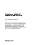
AlphaServer 8200/8400
Service Manual
Order Number EK–T8030–SV. A01
This manual is intended for Digital service engineers. It includes troubleshooting
information, configuration rules, and instructions for removal and replacement of
field-replaceable units (FRUs) for AlphaServer 8200 and 8400 systems.
digital equipment corporation
maynard, massachusetts
First Printing, May 1995
The information in this document is subject to change without notice and should not be
construed as a commitment by Digital Equipment Corporation.
Digital Equipment Corporation assumes no responsibility for any errors that may appear in
this document.
The software, if any, described in this document is furnished under a license and may be used
or copied only in accordance with the terms of such license. No responsibility is assumed for
the use or reliability of software or equipment that is not supplied by Digital Equipment
Corporation or its affiliated companies.
Copyright 1995 by Digital Equipment Corporation.
All Rights Reserved.
Printed in U.S.A.
The following are trademarks of Digital Equipment Corporation: AlphaGeneration,
AlphaServer, DEC, DECchip, DEC LANcontroller, OpenVMS, StorageWorks, VAX, the
AlphaGeneration logo, and the DIGITAL logo.
OSF/1 is a registered trademark of the Open Software Foundation, Inc. Prestoserve is a
trademark of Legato Systems, Inc. UNIX is a registered trademark in the U.S. and other
countries, licensed exclusively through X/Open Company Ltd.
FCC NOTICE: The equipment described in this manual generates, uses, and may emit radio
frequency energy. The equipment has been type tested and found to comply with the limits
for a Class A computing device pursuant to Subpart J of Part 15 of FCC Rules, which are
designed to provide reasonable protection against such radio frequency interference when
operated in a commercial environment. Operation of this equipment in a residential area may
cause interference, in which case the user at his own expense may be required to take
measures to correct the interference.
Contents
Preface ..............................................................................................................xv
Chapter 1
1.1
1.2
1.3
1.4
1.5
1.6
1.7
1.8
1.9
1.10
Overview of the Systems
AlphaServer 8400/8200 Overview............................................................1-2
TLSB System Bus ....................................................................................1-4
KN7CC Processor Module .......................................................................1-6
MS7CC Memory Module .........................................................................1-8
KFTHA Module .....................................................................................1-10
KFTIA Module ......................................................................................1-12
AlphaServer 8400 Power Subsystem Overview ......................................1-14
AlphaServer 8200 Power Subsystem Overview ......................................1-16
I/O Buses and In-Cab Storage Devices ................................................... 1-18
Troubleshooting Steps and Tools............................................................1-20
Part 1
Chapter 2
2.1
2.1.1
2.1.2
2.1.3
2.1.4
2.2
2.2.1
2.2.2
2.3
2.4
2.4.1
2.4.2
2.4.3
Troubleshooting
Troubleshooting with LEDs
Troubleshooting Common to Both Systems..............................................2-2
Start with the Control Panel...............................................................2-2
Troubleshooting TLSB Modules........................................................2-4
Troubleshooting a PCI Shelf..............................................................2-6
Troubleshooting StorageWorksShelves..............................................2-8
Troubleshooting the 8200 Power Subsystem...........................................2-10
8200 Power Regulators....................................................................2-10
8200 Cabling...................................................................................2-14
Troubleshooting the 8200 Cooling Subsystem........................................2-16
Troubleshooting the 8400 Power Subsystem...........................................2-18
8400 AC Input Box .........................................................................2-18
H7264 Power Regulators ................................................................. 2-20
H7263 Power Regulators ................................................................. 2-22
iii
2.4.4
2.5
2.6
2.7
2.8
Cabinet Control Logic (CCL) Module .............................................2-24
Troubleshooting the 8400 Blower...........................................................2-26
Troubleshooting 8400 XMI and Futurebus+ ...........................................2-28
Troubleshooting with 8400 XMI and Futurebus+ I/O Module LEDs ......2-30
Troubleshooting an 8400 DSSI PIU........................................................ 2-32
Chapter 3
3.1
3.1.1
3.1.2
3.1.3
3.1.4
3.2
3.2.1
3.2.2
3.3
3.4
3.5
3.6
3.6.1
3.6.2
Checking Self-Test Results: Console Display...........................................3-2
8200 Self-Test ...................................................................................3-2
Show Config Display for 8200 ..........................................................3-4
8400 Self-Test ...................................................................................3-6
Show Config Display for 8400 ..........................................................3-8
Running Diagnostics — the Test Command ...........................................3-10
Testing an Entire System.................................................................3-12
Sample Test Command for PCI ....................................................... 3-14
Identifying a Failing SIMM....................................................................3-16
Info Command .......................................................................................3-18
Show Power Display: 8400 Three-Phase Power.....................................3-20
Regulator Info Packets: 8400 Three-Phase Power...................................3-21
Brief Data Packet ............................................................................3-22
Full Information Data Packet........................................................... 3-24
Chapter 4
4.1
4.1.1
4.1.2
4.1.3
4.2
4.3
4.4
4.5
4.5.1
4.5.2
4.5.3
4.6
4.6.1
4.6.2
4.6.3
4.6.4
4.6.5
iv
Console Display and Diagnostics
DECevent Error Log
Brief Description of the TLSB Bus...........................................................4-2
Command/Address Bus .....................................................................4-2
Data Bus............................................................................................4-3
Error Checking..................................................................................4-3
Producing an Error Log with DECevent ...................................................4-4
Getting a Summary Error Log ..................................................................4-5
Supported Event Types ............................................................................4-6
Sample Error Log Entries.........................................................................4-8
Machine Check 660 Error..................................................................4-8
Machine Check 620 Error................................................................4-12
DWLPA Motherboard (PCIA) Adapter Error Log ...........................4-17
Parse Trees.............................................................................................4-23
Parse Tree for Machine Check 670 Errors .......................................4-23
Machine Check 660 Errors .............................................................. 4-24
Machine Check 630 Error................................................................4-51
Machine Check 620 Error................................................................4-52
Adapter Parse Trees.........................................................................4-61
Part 2
Chapter 5
5.1
5.2
5.3
5.4
5.5
5.6
5.7
5.8
5.9
5.10
TLSB Modules
How to Replace the Only Processor..........................................................5-2
How to Replace the Boot Processor..........................................................5-4
How to Add a New Processor or Replace a Secondary Processor..............5-8
Processor, Memory, or Terminator Module Removal and Replacement .5-12
SIMM Removal and Replacement.......................................................... 5-14
I/O Cable and KFTHA Module Removal and Replacement....................5-18
KFTIA Module Removal and Replacement............................................ 5-20
FDDI Daughter Card Removal and Replacement ...................................5-22
NVRAM Daughter Card Removal and Replacement ..............................5-24
NVRAM Battery Removal and Replacement .........................................5-26
Chapter 6
6.1
6.2
6.3
6.4
6.5
6.6
6.7
Updating Firmware
Booting LFU ............................................................................................6-2
List...........................................................................................................6-4
Update .....................................................................................................6-6
Exit ........................................................................................................6-10
Display and Verify Commands............................................................... 6-12
How to Update Corrupted Firmware.......................................................6-14
How to Modify Device Attributes ..........................................................6-18
Part 3
Chapter 7
7.1
7.2
7.3
7.4
7.5
7.6
7.7
AlphaServer 8200 System
Field-Replaceable Units
FRUs Accessible from the Front of the Cabinet........................................7-2
FRUs Accessible from the Rear................................................................7-4
FRUs in the Processor System Unit ..........................................................7-6
FRUs in the PCI Shelf ..............................................................................7-8
FRUs in the StorageWorks Shelf ............................................................7-10
FRUs in the Power Regulator ................................................................. 7-12
Cables ....................................................................................................7-14
Chapter 8
8.1
8.2
8.3
TLSB Modules
Configuration Rules
Main Cabinet ...........................................................................................8-2
Expander Cabinet.....................................................................................8-4
Power System...........................................................................................8-6
v
8.4
8.5
8.6
8.6.1
8.6.2
TLSB Card Cage and Storage Drawer ......................................................8-8
I/O Interface...........................................................................................8-10
Shelves...................................................................................................8-12
PCI Shelf.........................................................................................8-14
StorageWorks Shelf.........................................................................8-16
Chapter 9
9.1
9.2
Control Panel Removal and Replacement.................................................9-2
Cabinet Control Logic Module Removal and Replacement ......................9-4
Chapter 10
10.1
10.2
10.2.1
10.2.2
10.3
10.4
vi
PCI Shelves
PCI Shelf Removal and Replacement.....................................................12-2
Fan Removal and Replacement ..............................................................12-4
Chapter 13
13.1
13.2
13.3
Processor System Unit
Clock Module Removal and Replacement..............................................11-2
Terminator Module Removal and Replacement...................................... 11-4
TLSB Card Cage Removal and Replacement .........................................11-6
Prepare the Cabinet and Remove the Line Filter..............................11-6
Remove the TLSB Card Cage .........................................................11-8
Storage Drawer Removal and Replacement..........................................11-10
Chapter 12
12.1
12.2
Power System
Power Regulator Removal and Replacement ..........................................10-2
BBU Option Removal and Replacement ................................................10-4
Battery Pack Removal and Replacement .........................................10-4
Charger Board Removal and Replacement ......................................10-6
Power Strip Removal and Replacement..................................................10-8
Blower Removal and Replacement....................................................... 10-10
Chapter 11
11.1
11.2
11.3
11.3.1
11.3.2
11.4
Cabinet Control System
StorageWorks Shelves
StorageWorks Shelf Removal and Replacement.....................................13-2
Disk Removal and Replacement.............................................................13-4
Power Supply Removal and Replacement .............................................. 13-6
Part 4
Chapter 14
14.1
14.2
14.3
14.4
14.5
14.6
14.7
14.8
14.9
14.10
Cabinet Doors and Panels
Door and Cable Cover Removal and Replacement .................................16-2
Top Panel and Air Filter Removal and Replacement ..............................16-4
Side Panel Removal and Replacement....................................................16-6
Chapter 17
17.1
17.2
17.3
17.4
17.5
Configuration Rules
Main Cabinet .........................................................................................15-2
Expander Cabinet...................................................................................15-4
Battery Cabinet ......................................................................................15-6
Single-Phase Power System....................................................................15-8
Three-Phase Power System .................................................................. 15-10
TLSB Card Cage..................................................................................15-12
I/O Interface.........................................................................................15-16
Plug-In Units........................................................................................15-18
PCI Plug-In Unit............................................................................15-20
XMI Plug-In Unit ..........................................................................15-24
Futurebus+ Plug-In Unit ................................................................ 15-26
SCSI Storage Plug-In Unit.............................................................15-28
DSSI Disk Plug-In Unit ................................................................. 15-30
Battery Plug-In Unit ......................................................................15-32
Chapter 16
16.1
16.2
16.3
Field-Replaceable Units
FRUs Accessible from the Front of the Cabinet......................................14-2
FRUs Accessible from the Rear of the Cabinet.......................................14-4
FRUs in the Battery Cabinet................................................................... 14-6
FRUs in the PCI Plug-In Unit.................................................................14-8
FRUs in the XMI Plug-In Unit .............................................................14-10
FRUs in the Futurebus+ Plug-In Unit ...................................................14-12
FRUs in the SCSI Storage Plug-In Unit ................................................14-14
FRUs in the DSSI Disk Plug-In Unit ....................................................14-16
FRUs in the Battery Plug-In Unit .........................................................14-18
Cables .................................................................................................. 14-20
Chapter 15
15.1
15.2
15.3
15.4
15.5
15.6
15.7
15.8
15.8.1
15.8.2
15.8.3
15.8.4
15.8.5
15.8.6
AlphaServer 8400 System
Cabinet Control System
Control Panel Removal and Replacement...............................................17-2
CD-ROM Drive Removal and Replacement ...........................................17-4
Floppy Drive Removal and Replacement ...............................................17-6
Local Disk Converter Removal and Replacement...................................17-8
Cabinet Control Logic Module Removal and Replacement ..................17-10
vii
Chapter 18
18.1
18.1.1
18.1.2
18.2
18.2.1
18.2.2
18.2.3
18.3
Single-Phase Power System....................................................................18-2
H7264 Power Regulator Removal and Replacement........................18-2
Single-Phase AC Distribution Box Removal and Replacement........18-4
Three-Phase Power System ....................................................................18-6
H7263 Power Regulator Removal and Replacement........................18-6
Three-Phase AC Input Box Removal and Replacement ...................18-8
Three-Phase DC Distribution Box Removal and Replacement.......18-10
Blower Removal and Replacement....................................................... 18-12
Chapter 19
19.1
19.2
viii
DSSI Disk Plug-In Unit
Local Disk Converter Removal and Replacement...................................23-2
Remote Front Panel Removal and Replacement .....................................23-4
Disk Removal and Replacement.............................................................23-6
Power and Signal Harness Removal and Replacement............................23-8
Chapter 24
24.1
24.2
24.3
SCSI Storage Plug-In Unit
Device Removal and Replacement .........................................................22-2
Power Supply Removal and Replacement .............................................. 22-4
Chapter 23
23.1
23.2
23.3
23.4
XMI and Futurebus+ Plug-In Units
Power Regulator Removal and Replacement ..........................................21-2
Enclosure and Card Cage Removal and Replacement............................. 21-4
Air Filter Cleaning ................................................................................. 21-6
Chapter 22
22.1
22.2
PCI Plug-In Unit
Option Board Removal and Replacement...............................................20-2
Power Board Removal and Replacement................................................20-4
Motherboard Removal and Replacement................................................20-6
Chapter 21
21.1
21.2
21.3
TLSB Card Cage
System Clock Module Removal and Replacement..................................19-2
TLSB Card Cage Removal.....................................................................19-4
Chapter 20
20.1
20.2
20.3
Power and Cooling Systems
Battery Plug-In Unit
Fuse Removal and Replacement.............................................................24-2
Cable Removal and Replacement...........................................................24-4
Battery Removal and Replacement.........................................................24-6
Appendix A
A.1
A.2
Console Commands and Environment
Variables
Console Commands.................................................................................A-1
Environment Variables............................................................................A-5
Appendix B
How to Find Option Information
Index
Examples
3–1
3–2
3–3
3–4
3–5
3–6
3–7
3–8
3–9
3–10
3–11
4–1
4–2
4–3
4–4
4–5
4–6
4–7
5–1
5–2
5–3
6–1
6–2
6–3
6–4
6–5
6–6
6–7
8200 System Self-Test Console Display ...................................................3-2
Show Config Sample................................................................................3-4
8400 System Self-Test Console Display ...................................................3-6
Show Config Sample................................................................................3-8
Sample Test Commands......................................................................... 3-10
Sample Test Command for Entire System ..............................................3-12
Sample Test Command for PCI ..............................................................3-14
Console Mode: No Failing SIMMs........................................................ 3-16
Console Mode: Failing SIMMs Found...................................................3-17
Examples of the Info Command .............................................................3-18
Show Power Command ..........................................................................3-20
Producing an Error Log with DECevent ...................................................4-4
Summary Error Log .................................................................................4-5
OSF Event Type Identification.................................................................4-7
OpenVMS Event Type Identification .......................................................4-7
Sample Machine Check 660 Error Log Entry ...........................................4-8
Sample Machine Check 620 Error Log Entry ......................................... 4-13
Sample DWLPA Motherboard Error Log Entry......................................4-17
Replacing the Only Processor Module......................................................5-2
Replacing the Boot Processor...................................................................5-4
Adding or Replacing a Secondary Processor.............................................5-8
Booting LFU from CD-ROM ...................................................................6-2
List Command..........................................................................................6-4
Update Command ....................................................................................6-6
Exit Command .......................................................................................6-10
Display and Verify Commands............................................................... 6-12
Updating an “Unknown” Device ............................................................6-14
Modify Command ..................................................................................6-18
ix
Figures
1–1
1–2
1–3
1–4
1–5
1–6
1–7
1–8
1–9
1–10
1–11
1–12
1–13
2–1
2–2
2–3
2–4
2–5
2–6
2–7
2–8
2–9
2–10
2–11
2–12
2–13
2–14
2–15
2–16
2–17
2–18
2–19
2–20
2–21
2–22
2–23
2–24
2–25
2–26
2–27
2–28
2–29
x
AlphaServer 8400 and 8200 System Cabinets...........................................1-1
AlphaServer 8400 and 8200 Systems........................................................1-2
TLSB System Bus ....................................................................................1-4
General Appearance of TLSB Modules ....................................................1-5
KN7CC Processor Module .......................................................................1-6
MS7CC–BA (128-Mbyte) Memory Module .............................................1-8
KFTHA Module .....................................................................................1-10
KFTIA Module ......................................................................................1-12
AlphaServer 8400 Power System Overview ...........................................1-14
AlphaServer 8200 Power Subsystem Overview ......................................1-16
AlphaServer 82/8400 I/O Buses and In-Cab Storage...............................1-18
Troubleshooting Steps............................................................................1-20
Troubleshooting Tools ...........................................................................1-21
Control Panel ...........................................................................................2-2
Troubleshooting: Start with the Control Panel ..........................................2-2
TLSB Module Status................................................................................2-4
PCI FDDI and NVRAM Options on KFTIA .............................................2-5
PCI PIU in an 8400 ..................................................................................2-6
PCI Shelf in an 8200 ................................................................................2-7
Troubleshooting a PCI Shelf ....................................................................2-7
Troubleshooting StorageWorks Devices and Shelves ...............................2-8
8200 Power Regulators — AC Input Side...............................................2-10
8200 AC Input Troubleshooting Steps ....................................................2-11
8200 Power Regulators — DC Output Side ............................................2-12
Troubleshooting the DC Side of 8200 Regulators...................................2-13
Checking Power Connections.................................................................2-14
LEDs for Temperature and Cooling Fan Locations.................................2-16
Troubleshooting the 8200 Cooling System .............................................2-17
8400 AC Input Box ................................................................................2-18
8400 AC Input Box Troubleshooting Steps.............................................2-19
H7264 Power Regulators and Status LEDs .............................................2-20
Troubleshooting Steps for H7264 Regulator...........................................2-21
H7263 Power Regulator LEDs ...............................................................2-22
H7263 Power Regulator Troubleshooting Steps......................................2-23
8400 CCL Module LEDs........................................................................2-24
CCL Module Troubleshooting Steps.......................................................2-25
Blower ...................................................................................................2-26
Blower Troubleshooting Steps................................................................2-27
XMI and Futurebus+ Bus Power Regulator ............................................2-28
Troubleshooting I/O PIUs.......................................................................2-29
XMI and Futurebus+ Adapter LEDs.......................................................2-30
DSSI Disk Control Panel........................................................................2-32
3–1
3–2
3–3
3–4
3–5
3–6
3–7
3–8
3–9
3–10
3–11
4–1
4–2
4–3
4–4
4–5
4–6
4–7
5–1
5–2
5–3
5–4
5–5
5–6
5–7
5–8
5–9
7–1
7–2
7–3
7–4
7–5
7–6
8–1
8–2
8–3
8–4
8–5
8–6
8–7
8–8
8–9
8–10
9–1
Hose Numbering Scheme for KFTIA and KFTHA ...................................3-5
Hose Numbering Scheme for KFTIA and KFTHA ...................................3-9
Command Format ..................................................................................3-21
Sample Brief Data Packet....................................................................... 3-22
Brief Data Packet Structure ....................................................................3-23
Full Information Data Packet Structure ..................................................3-24
Full Data Packet: Values for Characters 1 – 6 .......................................3-25
Full Data Packet: Values for Characters 7 – 34.......................................3-26
Full Data Packet: Values for Characters 35 – 47.....................................3-27
Full Data Packet: Values for Characters 48 – 54.....................................3-28
Sample Full/History Data Packet............................................................3-28
Machine Check 670 Error ......................................................................4-23
Machine Check 660 Error ......................................................................4-24
Machine Check 630 Errors .....................................................................4-51
Machine Check 620 Error ......................................................................4-52
KFTxA Error Parse Tree ........................................................................4-61
DWLPA Error Parse Tree.......................................................................4-64
DWLMA Error Parse Tree .....................................................................4-67
Processor, Memory, or Terminator Module ............................................5-12
Removing a SIMM.................................................................................5-14
SIMM Connector Numbers — E2035 Module........................................5-16
SIMM Connector Numbers — E2036 (2-Gbyte) Module........................5-17
I/O Hose Cable.......................................................................................5-18
KFTIA Module ......................................................................................5-20
FDDI Daughter Card ..............................................................................5-22
NVRAM Daughter Card.........................................................................5-24
NVRAM Battery ....................................................................................5-26
AlphaServer 8200 Cabinet (Front) FRU Locations ...................................7-2
AlphaServer 8200 Cabinet (Rear) FRU Locations ....................................7-4
Processor System Unit FRU Locations .....................................................7-6
PCI Shelf FRU Locations .........................................................................7-8
StorageWorks Shelf FRU Locations ....................................................... 7-10
Power Regulator FRU Locations ............................................................7-12
Main Cabinet ...........................................................................................8-2
Expander Cabinet.....................................................................................8-4
System with Two Expander Cabinets (Front View) ..................................8-5
Power System...........................................................................................8-6
Power Strip ..............................................................................................8-7
TLSB Card Card Cage and Storage Drawer..............................................8-8
I/O Interface...........................................................................................8-10
Location of Shelf Space ......................................................................... 8-12
PCI Shelf and Slot Assignments .............................................................8-14
StorageWorks Shelf................................................................................8-16
Control Panel ...........................................................................................9-2
xi
9–2
10–1
10–2
10–3
10–4
10–5
10–6
11–1
11–2
11–3
11–4
11–5
11–6
12–1
12–2
13–1
13–2
13–3
14–1
14–2
14–3
14–4
14–5
14–6
14–7
14–8
14–9
15–1
15–2
15–3
15–4
15–5
15–6
15–7
15–8
15–9
15–10
15–11
15–12
15–13
15–14
15–15
15–16
15–17
xii
Cabinet Control Logic Module.................................................................9-4
Power Regulator.....................................................................................10-2
Accessing the BBU Option Battery Packs ..............................................10-4
Removing the BBU Option Battery Packs ..............................................10-5
Charger Board Removal .........................................................................10-6
Power Strip ............................................................................................10-8
Blower ................................................................................................. 10-10
Clock Module ........................................................................................11-2
Terminator Module ................................................................................11-4
TLSB Line Filter....................................................................................11-6
TLSB Card Cage (Rear View)................................................................11-8
TLSB Card Cage (Front View)...............................................................11-9
Storage Drawer ....................................................................................11-10
PCI Shelf................................................................................................12-2
PCI Fans ................................................................................................12-4
StorageWorks Shelf................................................................................13-2
StorageWorks Disk ................................................................................13-4
StorageWorks Power Supply ..................................................................13-6
Platform Cabinet (Front) Showing FRU Locations .................................14-2
Platform Cabinet (Rear) Showing FRU Locations ..................................14-4
Battery Cabinet Showing FRU Locations ...............................................14-6
PCI Plug-In Unit Showing FRU Locations .............................................14-8
XMI Plug-In Unit (Front) Showing FRU Locations..............................14-10
Futurebus+ Plug-In Unit (Front) Showing FRU Locations....................14-12
SCSI Disk Plug-In Unit (Front) Showing FRU Locations .....................14-14
DSSI Disk Plug-In Unit (Front) Showing FRU Locations .....................14-16
Battery Plug-In Unit (Rear) Showing FRU Locations ...........................14-18
Main Cabinet .........................................................................................15-2
Expander Cabinet...................................................................................15-4
System with Two Expander Cabinets (Front View) ................................15-5
Battery Cabinet ......................................................................................15-6
System with Two Battery Cabinets (Front View)....................................15-7
Single-Phase Power System....................................................................15-8
Three-Phase Power System ..................................................................15-10
TLSB Card Cage (Top View)...............................................................15-12
I/O Interface.........................................................................................15-16
Location of PIU Quadrants...................................................................15-18
PCI Plug-In Unit ..................................................................................15-20
PCI Shelf and Slot Assignments ...........................................................15-22
XMI Plug-In Unit.................................................................................15-24
Futurebus+ Plug-In Unit....................................................................... 15-26
SCSI Storage Plug-In Unit.................................................................... 15-28
SCSI Mounting Restrictions ................................................................. 15-29
DSSI Disk Plug-In Unit........................................................................ 15-30
15–18
16–1
16–2
16–3
17–1
17–2
17–3
17–4
17–5
18–1
18–2
18–3
18–4
18–5
18–6
19–1
19–2
20–1
20–2
20–3
21–1
21–2
21–3
22–1
22–2
23–1
23–2
23–3
23–4
24–1
24–2
24–3
24–4
Battery Plug-In Unit .............................................................................15-32
Cabinet Door and Cable Cover...............................................................16-2
Top Panel...............................................................................................16-4
Side Panel ..............................................................................................16-6
Control Panel .........................................................................................17-2
CD-ROM Drive......................................................................................17-4
Floppy Drive ..........................................................................................17-6
Local Disk Converter .............................................................................17-8
Cabinet Control Logic Module (Viewed from Front of Cabinet)...........17-10
H7264 Power Regulators........................................................................18-2
Single-Phase AC Distribution Box .........................................................18-4
H7263 Power Regulators........................................................................18-6
Three-Phase AC Input Box.....................................................................18-8
Three-Phase DC Distribution Box ........................................................18-10
Blower ................................................................................................. 18-12
System Clock Module ............................................................................19-2
TLSB Card Cage Removal.....................................................................19-4
PCI PIU Option Boards ..........................................................................20-2
PCI PIU Power Board ............................................................................20-4
PCI PIU Motherboard.............................................................................20-6
XMI and Futurebus+ PIU Power Regulators...........................................21-2
XMI and Futurebus+ PIU Enclosure.......................................................21-4
XMI and Futurebus+ PIU Air Filter........................................................21-6
SCSI PIU Devices ..................................................................................22-2
SCSI PIU Power Supply.........................................................................22-4
DSSI PIU — Underside of Brick Cover Showing Local Disk Converter.23-2
DSSI PIU — Underside of Brick Cover Showing Remote Front Panel ...23-4
DSSI PIU Disks......................................................................................23-6
DSSI PIU Power and Signal Harness......................................................23-8
Battery PIU Fuse....................................................................................24-2
Battery PIU (Rear) Showing Cable Routing ...........................................24-4
Battery Hold-Down Brackets..................................................................24-6
Rear Batteries (Blocks B and C).............................................................24-7
Tables
1
2
1–1
2–1
2–2
2–3
2–4
2–5
AlphaServer 8200 and 8400 Documentation............................................xvii
Related Documents ..................................................................................xix
Memory Modules and Related SIMMs .....................................................1-9
Control Panel LEDs at Power-Up.............................................................2-3
LEDs in a PCI Shelf.................................................................................2-6
SCSI Power Supply LEDs ........................................................................2-9
SCSI Device LEDs...................................................................................2-9
Troubleshooting the DWZZA–VA ...........................................................2-9
xiii
2–6
2–7
2–8
2–9
2–10
2–11
3–1
4–1
4–2
4–3
4–4
4–5
7–1
8–1
14–1
15–1
15–2
15–3
15–4
15–5
15–6
A–1
A–2
A–3
xiv
H7263 Power Regulator LED Summary.................................................2-22
I/O PIU Power Switches — Regulator B ................................................2-28
I/O PIU Power Regulator LEDs..............................................................2-29
DWLMA LEDs......................................................................................2-31
DWLAA Module LEDs..........................................................................2-31
Indicator Switches on DSSI Disk Control Panel .....................................2-33
Explanation of Sample Full/History Data Packet....................................3-29
TLSB Address Bus Commands ................................................................4-2
Supported Event Types ............................................................................4-6
Parsing a Sample 660 Error (Example 4–5) ..............................................4-8
Parsing a Sample 620 Error (Example 4–6) ............................................4-12
Parsing a DWLPA Motherboard Error (Example 4–7)............................4-17
Cables ....................................................................................................7-14
PCI/EISA Configuration Rules (KFE70 Installed) ..................................8-15
Cables ..................................................................................................14-20
Main Cabinet Variants ...........................................................................15-3
Expander Cabinet Variants.....................................................................15-5
Memory Module Options ..................................................................... 15-14
Placement of I/O Modules.................................................................... 15-14
Configuration Examples....................................................................... 15-15
PCI/EISA Configuration Rules (KFE70 Installed) ................................15-23
Summary of Console Commands ............................................................A-1
Environment Variables............................................................................A-6
Settings for the graphics_switch Environment Variable...........................A-8
Preface
Intended Audience
This manual is written for the customer service engineer.
Document Structure
This manual uses a structured documentation design. Topics are organized into
small sections for efficient online and printed reference. Each topic begins with an
abstract. You can quickly gain a comprehensive overview by reading only the
abstracts. Next is an illustration or example, which also provides quick reference.
Last in the structure are descriptive text and syntax definitions.
This manual has 24 chapters and two appendixes, as follows:
•
Chapter 1, Overview of the Systems, introduces the AlphaServer 8200 and
8400 systems and gives a brief overview of the system bus modules, and power
subsystem.
Part 1: Troubleshooting
•
Chapter 2, Troubleshooting with LEDs, tells how to use the LEDs and other
indicators on the AlphaServer 8200 to find problem components in the system.
•
Chapter 3, Console Display and Diagnostics, tells how to use these tools to
find nonfunctioning components in the system.
•
Chapter 4, DECevent Error Log, describes how to interpret the error log
produced by this utility program.
Part 2: TLSB Modules
•
Chapter 5, TLSB Modules, provides procedures for replacing I/O and memory
modules and for replacing or adding processor modules.
•
Chapter 6, Updating Firmware, describes how to use console commands and
the Loadable Firmware Update (LFU) Utility to update system firmware.
Part 3: AlphaServer 8200 System
•
Chapter 7, Field-Replaceable Units, describes the components of the
AlphaServer 8200 system that are replaceable by field service personnel.
xv
•
Chapter 8, Configuration Rules, provides configuration information for the
AlphaServer 8200 main and expander cabinet, power system, TLSB card cage
and storage drawer, I/O interface, and PCI and StorageWorks shelves.
•
Chapter 9, Cabinet Control System, describes how to remove and replace
components of the AlphaServer 8200 cabinet control system.
•
Chapter 10, Power System, tells how to remove and replace components of the
AlphaServer 8200 power system.
•
Chapter 11, Processor System Unit, tells how to remove and replace
components of the AlphaServer 8200 processor system unit.
•
Chapter 12, PCI Shelves, describes how to remove and replace PCI bus
shelves.
•
Chapter 13, StorageWorks Shelves, tells how to remove and replace
StorageWorks shelves and components within StorageWorks shelves.
Part 4: AlphaServer 8400 System
•
Chapter 14, Field-Replaceable Units, describes the components of the
AlphaServer 8400 system that are replaceable by field service personnel.
•
Chapter 15, Configuration Rules, provides configuration information for the
AlphaServer 8400 main and expander cabinet, power system, TLSB card cage,
I/O interface, and PCI plug-in unit.
•
Chapter 16, Cabinet Doors and Panels, tells how to remove and replace the
AlphaServer 8400 doors and top and side panels.
•
Chapter 17, Cabinet Control System, describes how to remove and replace
components of the AlphaServer 8400 cabinet control system.
•
Chapter 18, Power and Cooling Systems, tells how to remove and replace
components of the AlphaServer 8400 power and cooling subsystems.
•
Chapter 19, TLSB Card Cage, describes how to remove and insert modules in
the TLSB card cage, and how to remove and replace the card cage itself.
•
Chapter 20, PCI Plug-In Unit, tells how to remove and replace a PCI plug-in
unit in the AlphaServer 8400 system.
•
Chapter 21, XMI and Futurebus+ Plug-In Units, tells how to remove and
replace these field-replaceable units in the AlphaServer 8400 system.
•
Chapter 22, SCSI Storage Plug-In Unit, tells how to remove and replace SCSI
disks and tapes from a SCSI PIU.
•
Chapter 23, DSSI Disk Plug-In Unit, tells how to remove and replace DSSI
disks and tapes from a DSSI PIU.
xvi
•
Chapter 24, Battery Plug-In Unit, tells how to remove and replace the BBU
fuse, cable, and individual batteries in the battery plug-in-unit.
•
Appendix A, Console Commands and Environment Variables, is a quick
reference for commands.
•
Appendix B, How to Find Option Information, explains the ways to find
information about options.
Conventions Used in This Document
Icons. Icons similar to those shown below are used in illustrations for designating
part placement in the system described. A shaded area in the icon shows the location
of the component or part being discussed.
Front
Rear
BX-0099-95
Documentation Titles
Table 1 lists the books in the AlphaServer 8200 and 8400 documentation set. Table
2 lists other documents that you may find useful.
Table 1 AlphaServer 8200 and 8400 Documentation
Title
Order Number
Hardware User Information and Installation
Operations Manual
EK–T8030–OP
Site Preparation Guide
EK–T8030–SP
AlphaServer 8200 Installation Guide
EK–T8230–IN
AlphaServer 8400 Installation Guide
EK–T8430–IN
Service Information Kit
QZ–00RAC–GC
Service Manual (hard copy)
EK–T8030–SV
Service Manual (diskette)
AK–QKNFA–CA
xvii
Table 1 AlphaServer 8200 and 8400 Documentation (Continued)
Title
Order Number
Reference Manuals
System Technical Manual
EK–T8030–TM
DWLPA PCI Adapter Technical Manual
EK–DWLPA–TM
Upgrade Manuals for Both Systems
KN7CC CPU Module Installation Card
EK–KN7CC–IN
MS7CC Memory Installation Card
EK–MS7CC–IN
KFTHA System I/O Module Installation Guide
EK–KFTHA–IN
KFTIA Integrated I/O Module Installation Guide
EK–KFTIA–IN
Upgrade Manuals: 8400 System Only
AlphaServer 8400 Upgrade Manual
EK–T8430–UI
BA654 DSSI Disk PIU Installation Guide
EK–BA654–IN
BA655 SCSI Disk and Tape PIU Installation Guide
EK–BA655–IN
DWLAA Futurebus+ PIU Installation Guide
EK–DWLAA–IN
DWLMA XMI PIU Installation Guide
EK–DWLMA–IN
DWLPA PCI PIU Installation Guide
EK–DWL84–IN
H7237 Battery PIU Installation Guide
EK–H7237–IN
H7263 Power Regulator Installation Card
EK–H7263–IN
H9F00 Power Upgrade Manual
EK–H8463–UI
KFMSB Adapter Installation Guide
EK–KFMSB–IN
KZMSA Adapter Installation Guide
EK–KXMSX–IN
RRDCD Installation Guide
EK–RRDRX–IN
Upgrade Manuals: 8200 System Only
DWLPA PCI Shelf Installation Guide
EK–DWL82–IN
H7266 Power Regulator Installation Card
EK–H7266–IN
H7267 Battery Backup Installation Card
EK–H7267–IN
xviii
Table 2 Related Documents
Title
Order Number
General Site Preparation
Site Environmental Preparation Guide
EK–CSEPG–MA
System I/O Options
BA350 Modular Storage Shelf Subsystem Configuration Guide
EK–BA350–CG
BA350 Modular Storage Shelf Subsystem User's Guide
EK–BA350–UG
BA350-LA Modular Storage Shelf User's Guide
EK–350LA–UG
CIXCD Interface User Guide
EK–CIXCD–UG
DEC FDDIcontroller 400 Installation/Problem Solving
EK–DEMFA–IP
DEC FDDIcontrolle/Futurebus+ Installation Guide
EK–DEFAA–IN
DEC FDDIcontroller/PCI User Information
EK–DEFPA–IN
DEC LANcontroller 400 Installation Guide
EK–DEMNA–IN
DSSI VAXcluster Installation/Troubleshooting Manual
EK–410AA–MG
EtherWORKS Turbo PCI User Information
EK–DE435–OM
KZPSA PCI to SCSI User’s Guide
EK–KZPSA–UG
RF Series Integrated Storage Element User Guide
EK–RF72D–UG
StorageWorks RAID Array 200 Subsystem Family Installation
and Configuration Guide
EK–SWRA2–IG
StorageWorks RAID Array 200 Subsystem Family Software
User’s Guide for OpenVMS AXP
AA–Q6WVA–TE
StorageWorks RAID Array 200 Subsystem Family Software
User’s Guide for DEC OSF/1
AA–Q6TGA–TE
Operating System Manuals
Alpha Architecture Reference Manual
EY–L520E–DP
DEC OSF/1 Guide to System Administration
AA–PJU7A–TE
Guide to Installing DEC OSF/1
AA–PS2DE–TE
OpenVMS Alpha Version 6.2 Upgrade and Installation Manual
AA–PV6XC–TE
xix
Chapter 1
Overview of the Systems
This manual tells how to service two separate, but related, systems. The
AlphaServer 8400 and 8200 systems both use the same system bus (called the
TLSB).
The processor, memory, and I/O adapter units that can be configured on this bus are
also the same. The cabinets, and the components they are designed to carry, vary.
Figure 1–1 AlphaServer 8400 and 8200 System Cabinets
8400
8200
BX-0118-95
Overview of the Systems
1-1
1.1 AlphaServer 8400/8200 Overview
The AlphaServer 8400 has a 9-slot system bus, and the cabinet is designed to
house "plug-in units” that contain XMI, Futurebus+, and PCI/EISA buses, as
well as SCSI and DSSI I/O devices. The AlphaServer 8200 system has a 5-slot
system bus and is designed to house PCI/EISA buses and SCSI devices.
Figure 1–2 AlphaServer 8400 and 8200 Systems
AlphaServer 8200
Departmental Server
System
RackCabinet
mount
Cab
AlphaServer 8400
Enterprise Server
I/O
I/O
System Expander
Expander Cabinet
Cabinet
Cabinet
BX-0119B-94
1-2
Service Manual
The AlphaServer 8400 and 8200 systems are described in detail in the Technical
Summary for these systems. Here are some highlights, concentrating on
serviceability.
You will probably find the AlphaServer 8200 system in an office environment. The
AlphaServer 8400 systems are generally found in temperature and humidity
controlled (data center or laboratory) environments.
Troubleshooting aids for both systems include:
•
Easily seen and labeled LEDs and indicators.
•
A system self-test display that appears on the system console terminal at powerup. The console software also includes a test command for running various
diagnostics. If the power system includes H7263 regulators, detailed
information on the power system can be requested.
•
An error log produced by both the OpenVMS Alpha and Digital UNIX operating
systems for analyzing transient errors.
Removal and replacement procedures for field-replaceable units (FRUs) in the
AlphaServer 8200 system are for elements in the system unit (the top part of the
cabinet. Other elements that can be included in the cabinet are one or two AC/DC
power regulators, PCI bus shelves, and SCSI BA350–JB shelves. These are mounted
with brackets and screws attached to the cabinet.
AlphaServer 8400 systems can contain a wider variety of I/O buses and hence the
system self-test includes information on these buses and the I/O adapters in them.
In both systems, the components are accessible from the front and rear doors. Side
panels can be removed, if necessary, to check or fix cabling. Some components are
heavy and require two people for removal and replacement.
Overview of the Systems
1-3
1.2 TLSB System Bus
Both the AlphaServer 8400 and 8200 systems use the TLSB system bus. The
TLSB is a centerplane in the 8400 system; it offers 9 slots for modules. For an
8200 system, only the "back half" of the bus is used, to offer 5 slots for modules.
Figure 1–3 TLSB System Bus
AlphaServer 8400
Front
AlphaServer 8200
Processor,
Memory, and
KFTHA/KFTIA
Slot Modules
45 6 7 8
Front
(Not used)
Centerplane
(TLSB)
Power
Filter
3
2 1 0
Processor and Memory
Modules
8
KFTIA
Module
7 6 5
4
Processor,
Memory,
I/O Modules
BX-0111A-94
1-4
Service Manual
Figure 1–3 shows the location of the TLSB card cage in each system, and the node
numbers for the slots that contain either CPU, memory, or I/O modules, or fillers
which provide EMI protection, direct airflow, and terminate the TLSB system bus.
Figure 1–4 shows the front of the four types of modules. Also shown is a generic
“module.” Notice the molded cover on the right side of the module; each type of
module has a different cover, specially molded to follow the shape of the
components on the module. These covers ensure swift, even airflow around the
components for proper cooling. Thus, if you have occasion to remove the covers
from a module, be sure that you put them back correctly.
Figure 1–4 General Appearance of TLSB Modules
CPU
Memory KFTHA KFTIA
Side 2
Side 1
BX-0132A-94
Overview of the Systems
1-5
1.3 KN7CC Processor Module
Up to six KN7CC modules can be used in an AlphaServer 8400 system, and up
to three in an AlphaServer 8200 system. A processor module contains either
one or two CPU chips.
Figure 1–5 KN7CC Processor Module
3
1
5
4
2
5
Side 2
6
Side 1
BX-0159-AI
1-6
Service Manual
The KN7CC processor module can have either one (KN7CC–AA) or two (KN7CC–
AB) CPU chips. At the time of this printing, the chips are the DECchip 21164 chips,
with a cycle time of 300 MHz.
NOTE: Since the bus cycle time is an integer multiple of the chip cycle time, it is
crucial that the system clock card (see Sections 1.7 and 1.8) and the processor
modules are properly matched. If a bus clock card and processor module(s) cannot
be synchronized, the system will start power-up, but will probably not complete,
halting in the middle of the power-up console display in a way that is hard to
diagnose. The part number for the clock card synchronized to 300 MHz CPUs is
54–21728–05.
If one of the CPUs in a dual-CPU processor module is malfunctioning, you
replace the entire module. The chip is not a field-replaceable unit (FRU); the
module is. You will see indications of dual processors on the console display, as
shown in Section 3.1.
Figure 1–5 shows a two-CPU processor module. The raised blocks in the figure
represent heat sinks that cover the CPU chips. Note that the lightly shaded CPU and
B-cache areas are not populated if this is a single-CPU module.
Ê
Ë
Ì
Í
Î
Ï
CPU chip(s). The DECchip 21164 operates at supercomputer speeds. It is
an Alpha architecture chip with super-pipelined micro-architecture. The CPU
controls two levels of on-chip caching and one level of off-chip caching. The
8-Kbyte instruction cache and 2x8-Kbyte data cache are fed from the on-chip
96-Kbyte secondary cache.
B-cache. The backup cache on the module is a 4-Mbyte nonpipelined cache
using 256Kx4 SRAMs.
MMG. The MMG gate array multiplexes the addresses to and from the two
CPU chips to the interface control chip (ADG). In addition, the MMG
supplies write data and is used to perform some Gbus addressing and
sequencing functions.
ADG. The address gate array contains the interface control logic for the CPU
chips, the memory multiplexing gate array (MMG), the TLSB bus, and the
data interface gate arrays (DIGAs).
DIGAs. The four data interface gate arrays together assemble the 128-bit
incoming and 256-bit outgoing data from and to the TLSB.
DC-to-DC Converters. These converters step the 48 VDC power supplied by
the power subsystem to the voltages required by the components on the
processor board.
Overview of the Systems
1-7
1.4 MS7CC Memory Module
The MS7CC memory module comes in five variants offering 128 Mbytes, 256
Mbytes, 512 Mbytes, 1 Gbyte, and 2 Gbytes. Up to seven memory modules can
be installed in an 8400 system; three in an 8200.
Figure 1–6 MS7CC–BA (128-Mbyte) Memory Module
2
3
4
1
3
2
5
1
BX-0160-94
1-8
Service Manual
All memory modules for the AlphaServer 8400 and 8200 systems have SIMMs
(single inline memory modules). DRAMs are mounted on small cards that are fixed
to the larger memory module by spring-held mounting clips that grip both sides of
the SIMM. Figure 1–6 shows:
Ê
Ë
Ì
Í
Î
The array of SIMMs in an MS7CCA–BA (128-Mbyte) memory module.
The dust cover that protects the connectors into which SIMMs can be plugged to
upgrade the 128-Mbyte module to a 256-Mbyte module.
Memory data interface (MDI) gate arrays that provide the data interface
between the TLSB bus and the DRAM arrays. The MDIs contain data buffers,
ECC checking logic, self-test data generation and checking logic, and control
and status registers (CSRs).
The control address interface (CTL) gate array that provides the interface to the
TLSB, controls DRAM timing and refresh, runs memory self-test, and contains
TLSB and memory-specific registers.
The DC-to-DC converter.
All types of SIMMs for all the memory modules available for AlphaServer 8400
and 8200 systems are field-replaceable. Section 3.3 describes how to isolate a
problem SIMM. When you replace a SIMM, you must be sure that the type of
SIMM matches the module it is designed for, as detailed in Table 1–1.
Table 1–1 Memory Modules and Related SIMMs
Memory (Size)
Motherboard
Part Number
SIMM Part Number
Number
of SIMMs
MS7CC–BA (128 MB)
E2035–AA
54–21724–01 (8 MB)
16
MS7CC–CA (256 MB)
E2035–AA
54–21724–01 (8 MB)
32
MS7CC–DA (512 MB)
E2035–AA
54–21726–01 (32 MB)
16
MS7CC–EA (1 GB)
E2035–AA
54–21726–01 (32 MB)
32
MS7CC–FA (2 GB)
E2036–AA
54–21718–01 (64 MB)
36
Overview of the Systems
1-9
1.5 KFTHA Module
The KFTHA module offers four “hose” connectors that interface between the
TLSB bus and external buses: XMI, Futurebus+, and PCI/EISA.
Figure 1–7 KFTHA Module
2
3
4
1
3
5
BX-0162-94
1-10
Service Manual
The KFTHA module is designed for high-speed, high-volume data transfers. Direct
memory access (DMA) transfers are pipelined to allow for up to 500 Mbytes/second
throughput. The major elements of the KFTHA module are:
Ê
Ë
Ì
Í
Î
RAM to buffer data for the DMA transfers.
Four hose-to-data-path (HDP) chips, each handling 32 bits from two “hoses”
(I/O cables connecting to an adapter in an associated I/O bus). Data on the
HDPs flow in one direction; either “up” (to the KFTHA) or “down” (to the
I/O adapter).
Four I/O data path (IDP) chips, which together handle a 256-bit data transfer
to or from the TLSB system bus.
An I/O control chip (ICC) houses the primary control logic for the TLSB
interface.
A DC-to-DC converter that converts the 48 VDC system power to the DC
voltage required by the KFTHA module.
Overview of the Systems
1-11
1.6 KFTIA Module
The KFTIA module offers an internal peripheral component interconnect (PCI)
bus that connects to various kinds of I/O devices through connectors at the front
of the module. The module also has one “hose” connector that can interface to a
PCI/EISA, XMI, or Futurebus+ bus.
Figure 1–8 KFTIA Module
5
FDDI options
6
1
3
2
7
4
Front view
Side view from rear
BX-0154-94
1-12
Service Manual
The KFTIA I/O module offers an internal PCI bus that is integrated into the module
itself, as well as a direct “hose” connector from the KFTIA to separate buses. As
Figure 1–8 shows, several types of connectors reveal the I/O options accessible
directly from the module.
The basic module offers:
Ê
Ë
Ì
Í
Three FWD (fast wide differential) SCSI connectors, that, combined with
Digital StorageWorks RAID controllers, storage cabinets, and devices, offer
access to large amounts of SCSI disk storage.
One single-ended SCSI connector, reserved for the system load device.
Two Ethernet connectors.
One “hose” connector that can interface to an XMI, Futurebus+, or PCI/EISA
bus.
Three other options are available, which can be ordered and are field-installable:
Î
Ï
Ð
DEFPZ–AA daughter card. A multimode fiber FDDI (fiber-distributed data
interface) on-board logic card and its associated connector. (Allows up to 2 km
local area network (LAN).
DEFPZ–UA daughter card. A copper wire FDDI (fiber-distributed data interface) on-board logic card and its associated connector. (Allows up to 100-m
cabling in office-type LAN).
NVRAM daughter card (part number DJ–ML300–BA). A 4-Mbyte memory
card that can enhance performance, increasing the memory available as buffer
space for DMA (direct memory access) transmissions.
Overview of the Systems
1-13
1.7 AlphaServer 8400 Power Subsystem Overview
An AlphaServer 8400 power subsystem has either single-phase or three-phase
AC power input.
Figure 1–9 AlphaServer 8400 Power System Overview
4
5
7
8
2
6
3
1
9
9
10
Front
Rear
BX-0121A-94
Ê
Either single-phase or three-phase AC power enters the system by cable through
the AC input box. Figure 1–9 shows a system with single-phase power. Each has
a cabinet circuit breaker and fuses for protection from power surges. The threephase system offers a port for monitoring voltage and the choice of battery
backup.
1-14
Service Manual
Ë
Ì
Two kinds of power regulators are available. An H7264 regulator (shown in
Figure 1–9 with the cover plate removed) converts single-phase AC power to 48
VDC. A system may use one or two H7264 power regulators, as needed for
power demands (see the Systems and Options Catalog for power requirements).
The H7263 regulators convert three-phase AC power to 48 VDC and also supply
information for console display. Two or three regulators offer n+1 redundancy;
that is, if one regulator fails, the second or third supplies the needed power.
The DC distribution box in back of the H7264 power regulator provides 48VDC
to the system, holding connector points for power distribution (under the gray
cover) and provides a signal interface between the CCL and the power
regulators. With three-phase power input and H7263 regulator(s), connector
points are also available for input from battery-backup units (BBUs) located in
either a BBU plug-in unit (PIU) or from battery expander cabinets.
The cabinet control logic (CCL) module contains logic that monitors signals
from parts of the power system.
The clock module provides the oscillator and logic that governs the frequency
with which signals can be transmitted on the TLSB (bus cycle time). The
clocking scheme supports a bus cycle time of 10 ns, which translates to a system
clock frequency of 100 MHz.
The power filter removes any noise disturbance on the 48V line to supply
consistent power to the delicate system modules and other components.
The power bus bar delivers 48 VDC power to modules on the system bus. All
slots in the system bus must be filled for proper termination of the bus (filler
modules are supplied as part of the base system).
Modules on the system bus contain DC-to-DC converters that step the power
down to the voltages required by the particular component.
This connection provides power to the system blower that cools the entire
system.
48 VDC power is supplied to system plug-in unit housing through receptacles
located on a crossbar of the PIU housing. (This receptacle is covered by a plate
that is removed when a PIU is installed.)
Overview of the Systems
1-15
1.8 AlphaServer 8200 Power Subsystem Overview
The power subsystem consists of those system components that deliver electrical
current to the rest of the system.
Figure 1–10 AlphaServer 8200 Power Subsystem Overview
8
5
4
7 6
3
4
Individual
Circuit Breakers
9
1
10 Regulator
Circuit Breaker
OVERTEMP
OVERVOLTAGE
MODULE OK
OVERTEMP
MODULE OK
OVERVOLTAGE
3
Front
2
Rear
BX-0146D-95
1-16
Service Manual
Single-phase AC power enters the system through the AC input box. The front
view in Figure 1–10 shows one power regulator. The rear view shows two, to
illustrate how the AC power enters the power strip, and then is routed down to
the two regulators. Two regulators provide n+1 redundancy (that is, if one
fails, the other will supply power).
Each power regulator contains an AC input, two 48 VDC outputs, and
(optional) battery backup.
The two DC distribution connectors in the front of the power regulator provide
48 VDC to the system. LEDs signal the status of the regulator feeding these
connectors.
The cabinet control logic (CCL) module monitors signals from parts of the
power system and provides error information to the console software. It is
located behind the CCL panel.
The clock module provides the oscillator and logic that governs the frequency
with which signals can be transmitted on the TLSB (bus cycle time). The
clocking scheme supports a bus cycle time of 10 ns; system clock frequencies
may vary. The clock card must support the timing of the processors in the
TLSB bus; otherwise, the system will not power up properly.
The power filter removes any noise disturbance on the 48V line, supplying
consistent power to system modules and other components.
The power bus bar delivers 48 VDC power to modules on the system bus. All
slots must be filled for proper termination of the bus; terminator modules are
supplied as part of the base system.
Modules on the system bus contain DC-to-DC converters that step the power
down to the voltages required by the particular component.
As shown, 48 VDC power is supplied to the StorageWorks shelves mounted in
the cabinet. The power regulators convert the 48 VDC to the 12, 3, and 5 VDC
power used by the StorageWorks I/O devices.
The same type of clips and receptacles used for the StorageWorks shelves
supply 48 VDC power to the PCI card cage. A regulator inside the card cage
converts the 48 VDC to the power used internally.
Overview of the Systems
1-17
1.9 I/O Buses and In-Cab Storage Devices
Both the AlphaServer 8200 and 8400 system and expander cabinets are designed
to hold PCI/EISA bus shelves and StorageWorks I/O device shelves. In
addition, the AlphaServer 8400 cabinets can hold XMI and Futurebus+ buses.
Figure 1–11 AlphaServer 82/8400 I/O Buses and In-Cab Storage
8200 System Cab
8400 System Cab
9
StorageWorks
XMI or Futurebus+
(8400 only)
digital
INPUT VOLTAGE
48 VDC
INPUT CURRENT
28A MAX
MOD OK
OC
OT
OV
48V
INPUT VOLTAGE
48 VDC
INPUT CURRENT
5A MAX
MOD OK
OC
OT
OV
48V
RESET
V-OUT
DISABLE
OVERTEMP
OVERVOLTAGE
MODULE OK
OVERTEMP
OVERVOLTAGE
MODULE OK
PCI
BX-0183-94
1-18
Service Manual
Figure 1–11 shows an AlphaServer 8200 system cabinet and an AlphaServer 8400
system cabinet.
As shown, the PCI/EISA bus and StorageWorks shelves are mounted horizontally in
the 8200 and vertically – within enclosures called “plug-in units” (PIUs) – in the
8400. Each StorageWorks shelf has room for up to seven devices, including a signal
converter and 3.25-inch disks or tapes. A power unit (DC-to-DC converter) is in the
bottom (leftmost) slot of the shelf.
The AlphaServer 8200 cabinets are structured to hold horizontal shelves of roughly
the same height. The system cabinet has five shelf slots; the bottom two can be
power regulators, and the top three can be any combination of PCI/EISA shelves
(starting from the bottom up) or StorageWorks shelves (starting from the top down).
Two StorageWorks shelves can be mounted, back to back, in the same shelf slot.
The 8200 expander cabinet is also structured to hold horizontal shelves of about the
same height. The configuration rules for the AlphaServer 8200 are described in
Chapter 8.
The AlphaServer 8400 cabinets can also contain XMI and Futurebus+ buses in PIUs.
The system cabinet has four quadrants in the lower part of the cabinet (the XMI PIU
takes two quadrants). Expander cabinets have six quadrants.
Both systems can be connected to the I/O devices of their resident buses and
adapters, but these are not housed within the cabinets themselves. StorageWorks
cabinets are also available that can hold RAID controllers and other options not
available within the system cabinets.
Overview of the Systems
1-19
1.10 Troubleshooting Steps and Tools
Follow steps to isolate system problems. A possible routine is shown below.
Figure 1–12 Troubleshooting Steps
You cannot find cause of
user problem by phone. Go
to site and follow these steps.
Control
panel LEDs
lit
No
Check power subsystem
(see Chapter 2)
Yes
Yes
Operating system
running
Customer experiences
intermittent error: Check
error log (Chapter 4)
No
Console software
running
Yes
Type "init" command.
Check system self-test
display (see Chapter 3)
No
Restart system. Check
system self-test display
(see Chapter 3)
Identify
faulty FRU
No
Boot operating system,
check error log (see
Chapter 4)
Yes
Power down system and
replace FRU. Power up.
If system self-test passes,
boot operating system.
Yes
Identify
faulty FRU
No
Done
Problem is beyond the
scope of this Service
Manual. Call customer
support center for help.
BX-0123-94
1-20
Service Manual
The system hardware, console software, and operating system software provide three
types of troubleshooting tools, as shown in Figure 1–13.
Chapters 2, 3, and 4 tell how to use these tools to isolate faulty components or report
software problems for AlphaServer 8200 and 8400 systems.
Figure 1–13 Troubleshooting Tools
General Types of
Problems
Tools for Finding Problems
Environmental Problems (Temp., Humidity, Air Pressure)
LEDs and Indicators
Power Supply or
Signal Interruptions
System Self-Test and
Other Console Displays
Hardware Problems
Error Log Printout
Software Problems
BX-0129A-94
Overview of the Systems
1-21
Part 1
Troubleshooting
Chapter 2
Troubleshooting with LEDs
This chapter tells how to use LED displays and other indicators to track down faulty
components that you can replace in the AlphaServer 8200 and 8400 systems.
LEDs give status on the power subsystem, system bus (TLSB) modules (processor,
memory, and I/O), and I/O buses and devices in shelves. The cooling subsystem
consists of fans in various locations and can be checked by looking and listening for
the fans.
Where the systems are similar (TLSB bus and modules), the troubleshooting
procedures described here apply to both. Where they are different (power
subsystem), details of troubleshooting vary.
The sections in this chapter are as follows:
•
Troubleshooting Common to Both Systems
•
− Start with the Control Panel
− Troubleshooting TLSB Modules
− Troubleshooting a PCI Shelf
− Troubleshooting StorageWorks Shelves
Troubleshooting the 8200 Power Subsystem
•
− 8200 Power Regulators
− 8200 Cabling
Troubleshooting the 8200 Cooling Subsystem
•
Troubleshooting the 8400 Power Subsystem
•
− 8400 AC Input Box
− H7264 Power Regulators
− H7263 Power Regulators
− Cabinet Control Logic (CCL) Module
Troubleshooting the 8400 Blower
•
Troubleshooting 8400 XMI and Futurebus+
•
Troubleshooting with 8400 XMI and Futurebus+ I/O Module LEDs
•
Troubleshooting an 8400 DSSI PIU
Troubleshooting with LEDs
2-1
2.1 Troubleshooting Common to Both Systems
2.1.1 Start with the Control Panel
Check the control panel lights. The 8200 has three pushbuttons and three LEDs.
The 8400 has a keyswitch and three LEDs.
Figure 2–1 Control Panel
8200 Pushbuttons
8400 Keyswitch
Disable
Front
2.88
On/Off
Enable
Secure
Run
Restart
Fault
TM
Front
LEDs
Secure
Enable
Restart
Key On
Run
Fault
BX-0190-95
Figure 2–2 Troubleshooting: Start with the Control Panel
Power
button/ keyswitch
is Off /Disable
(82/8400)
No
Yes
1
Fix problem identified.
If a faulty component or firmware update
was identified as the problem, replace the
component or update the firmware. If the
problem has not yet been identified, go to 2
2 Turn power on and watch power-up.
A
As 48-VDC power is passed to the system,
initial tests are run on the CPU, memory,
and I/O adapters on the system. If the system
passes this power-up testing, the green Enable
LED should light. If it does not, look at the console
terminal display to pinpoint the failing module and
replace the module. Repeat 2 . ( If no console
display, the console terminal may be a TGA
(graphics) terminal, connected through a PCI bus.
Connect a character-cell terminal through the serial
port on the system cabinet. Repeat 2
BX-0175-94
2-2
Service Manual Part 1: Troubleshooting
Table 2–1 Control Panel LEDs at Power-Up
Action
Set circuit breaker to On
Press On button (8200) /Turn keyswitch
to Enable (8400)
System self-test starts
Modules pass self-test
Module fails self-test
Three-phase power problem
Operating system boots
Key On (8400)
/Enable (8200)
Run
Fault
Off
On
Off
Off
On
On
On
On
On
Off
Off
Off
Off
On
Off
Slow
Blink
On
Off
On
Blink
Off
Figure 2–2 Troubleshooting: Start with the Control Panel (Cont.)
A
Fault LED
is lit
3
Yes
No
Any LEDs lit
on control panel
System clock and CPUs are not synchronized.
If Key On/Enable is green, Fault is lit, and
system self-test did not complete, check to see if
the system clock and the CPUs have different cycle
times. Replace as appropriate and proceed with 2
No
Yes
Green LED(s)
lit
Some component failed system self-test.
If Key On/Enable is green, Fault is lit, and
system self-tests have completed, replace
any failed component and proceed with 2
Yes
4 Status LEDs are not receiving power/signals.
Check the regulators to see if DC power is
leaving the regulator. If so, check the power and
signal lines to the CCL. Check the cabling between
the CCL module and the control panel. If connections
seem OK, replace CCL. If still no lights on control
panel, replace control panel. Proceed with 2
5 System self-test passed (Key On/Enable is lit);
operating system running (Run is lit).
If both green LEDs are lit, system self-test has
passed, and the operating system is running. Check
the error log (see Chapter 4). Ensure that the
proper boot disk is selected to boot the operating system.
If Run is not lit, boot the operating system.
When the operating system boots, look at the error log.
BX-0175B-95
Troubleshooting with LEDs
2-3
2.1.2 Troubleshooting TLSB Modules
You can check individual module self-test results by looking at the status LEDs
on the modules.
Figure 2–3 TLSB Module Status
LEDs
LED
CPU
Memory
KFTHA
KFTIA
BX-0132-94
2-4
Service Manual Part 1: Troubleshooting
In general, if a module on the TLSB does not pass self-test (green led is not lit) it
should be replaced.
There are two cases where some removal and replacement action may be needed
even though the module passes self-test.
Failure of the built-in-self-test for the MS7CC modules indicates that testing has
shown that there is no single 64-Kbyte segment of memory that is usable. Each 64Kbyte segment must show at least 256 bad pages before it is noted as unusable.
However, it is possible for a SIMM to warrant replacement, even though the module
as a whole passes its self-test.
Also, a KFTIA may contain field-replaceable options that are faulty, even when the
module has passed its self-test. The PCI FDDI option and the PCI NVRAM cards
can be replaced (see below), and, for other options, you may simply disconnect the
I/O option that failed its own self-test, rather than bringing down the whole I/O
operation handled by the KFTIA, until a replacement module can be found.
You can determine faulty SIMMs and KFTIA options with the show config console
command, as described in Chapter 3.
Figure 2–4 PCI FDDI and NVRAM Options on KFTIA
FDDI
option
NVRAM
option
BX-0171-95
Troubleshooting with LEDs
2-5
2.1.3 Troubleshooting a PCI Shelf
LEDs show the status of the power supplies, as well as the adapter self-test
results in the PCI shelf, mounted vertically in the AlphaServer 8400,
horizontally in the AlphaServer 8200.
Figure 2–5 PCI PIU in an 8400
Hose
DWLPA
LED
Numbers
48V Power
1
2
3
4
BX-0165A-95
Table 2–2 LEDs in a PCI Shelf
LED No.
1
2
3
4
2-6
Meaning When Lit
On-board power system OK
Motherboard self-test passed
48 VDC power supply OK
Hose error
Service Manual Part 1: Troubleshooting
Figure 2–6 PCI Shelf in an 8200
1
2
3
4
DWLPA LED numbers
BX-0174-95
Figure 2–7 Troubleshooting a PCI Shelf
LED 3 lit
No
11 Check Cabling to PCI shelf.
Check to make sure the clip connectors
are engaged properly. If so, proceed to 2
Yes
2
No
LED 1 lit
Check 48V Power Supply.
13 Internal Power System Error.
On 8200, check fans. Replace if not
running. On 8400, check for jumper
cable replacing fan connection.
Yes
4 Replace Power Board.
No
LED 2 lit
15 Replace Motherboard.
Yes
Yes
LED 4 lit
16 Hose Error.
Some error has occurred in the protocol
governing the transfer of data over the
hose. Replace the hose first, the motherboard second, the KFTHA or KFTIA third.
BX-0141-94
Troubleshooting with LEDs
2-7
2.1.4 Troubleshooting StorageWorksShelves
StorageWorks devices are mounted in shelves that are mounted horizontally in
the 8200 system or expander cabinet. In the 8400, a different StorageWorks
shelf is mounted vertically in a PIU. StorageWorks devices can also be mounted
in separate StorageWorks cabinets.
Figure 2–8 Troubleshooting StorageWorks Devices and Shelves
From a
FWD SCSI
Adapter
2-8
Service Manual Part 1: Troubleshooting
DWZZA-VA
BX-0733C-95
There are many StorageWorks devices that can be connected to AlphaServer 8200
and 8400 systems. Here, the discussion is limited to troubleshooting devices and
shelves that are mounted in a StorageWorks shelf in a SCSI PIU in an AlphaServer
system cabinet or expander cabinet.
Table 2–3 SCSI Power Supply LEDs
Indicator LED
LED State
Meaning
Left (Top) Green LED
Off
Shelf fault
On
Shelf OK
Off
Power fault
On
Power OK
Right (Bottom) Green
LED
Table 2–4 SCSI Device LEDs
Indicator LED
LED State
Meaning
Left (Top) Green LED
Blinking
Data is being transferred to the device.
Off
No data transfer to the device is taking
place.
Blinking
Data is being transferred from the
device.
Off
No data transfer from the device is
taking place.
Right (Bottom) Yellow
LED
Table 2–5 Troubleshooting the DWZZA–VA
Indicator LED
Meaning
None
If the power supply LEDs are lit, but the device LEDs are not
lit, check to see that the connecting cable is properly seated in
the DWZZA–VA and, at the other end, in the FWD adapter.
Troubleshooting with LEDs
2-9
2.2 Troubleshooting the 8200 Power Subsystem
2.2.1 8200 Power Regulators
The 8200 power regulators accept single-phase AC and produce 48 VDC power.
Figure 2–9 8200 Power Regulators — AC Input Side
Rear View
Rear
3
1
2
4
Ê
Ë
Ì
Í
2-10
BX-0146C-95
AC input cable to AC power strip. (Used wth two regulators.)
Power plugs and cables providing AC input to the individual regulators.
Circuit breakers on power strip. Lower controls left plug; higher controls
right two plugs.
Regulator circuit breaker. (Use power strip breakers if two regulators.).
Service Manual Part 1: Troubleshooting
Figure 2–10 8200 AC Input Troubleshooting Steps
Single Power Regulator
Circuit
Breaker On
Circuit Breaker
Tripped
Rear
(On)
(Off)
Two Power Regulators
Circuit Breaker
Tripped (right two plugs)
Power Strip
Circuit
Breaker On
(Left plug)
(Off)
(On)
Rear
Circuit breaker
tripped
No
Check DC side of
regulator(s)
Yes
1
Check for breaker trip due to power surge.
Check to make sure no one has intentionally powered
the system down. If not, the breaker may have
been tripped by an outside power surge or a short
within the system. Push the breaker switch to On.
A. If the breaker does not trip off again, check if
power has returned to other parts of the system.
Blower spins up? System self-test completes OK
and console prompt comes up? If so, boot the
operating system. If not, continue with the DC
regulators.
B. If the breaker does trip to off again, check for
a short circuit within the system. Continue the
search with the DC side of the regulators.
BX-0179-95
Troubleshooting with LEDs
2-11
Figure 2–11 8200 Power Regulators — DC Output Side
48 VDC Output
to CCL
2-12
Service Manual Part 1: Troubleshooting
REPLACE BATTERY
2
ON BATTERY
OVER TEMP
9 SIGNALS 1
10
BATTERYCHARGING
CURRENT
SHARE
+ 48VDC-
OVERVOLTAGE
+ 48VDC-
MODULE OK
Front
BX-0176-95
Figure 2–12 Troubleshooting the DC Side of 8200 Regulators
MOD OK LED
unlit
Overtemp
LED lit
Yes
1
If the room temperature is high, there may
be a problem with the air conditioning unit
or with airflow conditions in the lab. Correct
that problem and restart the system. If Overtemp relights, proceed to 2
No
Overvoltage
LED lit
Check ambient temperature.
Yes
2
Check to see if blowers are running.
If the ambient temperature is OK, then check
to see if the blowers are running. If not, then
the 48VDC output from the regulator has been
shut off because the internal temperature of the
regulator is too high. The regulator is malfunctioning; replace it.
3
Turn off AC power, wait 30 seconds, retry.
If this LED is lit, more than 48 VDC is being
output from the regulator. Turn off the AC power,
wait 30 seconds; turn on the AC breaker and power
system up again. If you do this several times and
the Overvoltage LED relights, proceed to
4
4
Disconnect the 48V lines leaving the regulator.
An Overvoltage condition could occur if there is
a short in the lines leaving the regulator. Turn off
AC power and disconnect the cables from the
leads at the DC side of the regulator, then turn on
the AC breaker. If the Overvoltage LED lights,
the problem is the regulator. Replace it.
Otherwise, turn off the power and check the cabling
for shorting.
BX-0181-95
Troubleshooting with LEDs
2-13
2.2.2 8200 Cabling
If some component of the system is not working, or its LEDs are not lit, check
the cabling to the device or component.
Figure 2–13 Checking Power Connections
Rear View
Front View
5
5
4
1
OVERTEMP
OVERVOLTAGE
MODULE OK
OVERTEMP
OVERVOLTAGE
MODULE OK
3
2
BX-0146B-94
2-14
Service Manual Part 1: Troubleshooting
Ê
Ë
Ì
Í
Î
Check to make sure that the main AC power cable is plugged into the AC
power strip (two regulators) or the one regulator in the system.
Make sure that, if battery backup is in use, it is functioning.
Make sure that the 48 VDC cables are plugged into the outlets in the regulator.
Check the connections to the PCI shelf and StorageWorks shelves.
Check all the cabling that can be seen. Cabling to the TLSB bus enters the
control panel, goes beneath the bottom of the bus (see arrow), and reappears
near the clock card at the back to supply power to the 48 VDC power bus bar
on the centerplane. If there appears to be a problem with power supply to the
bus, remove the front panel and check that power and signal cabling
connections are in order.
Troubleshooting with LEDs
2-15
2.3 Troubleshooting the 8200 Cooling Subsystem
The cooling subsystem of the AlphaServer 8200 system consists of several fans.
One is located directly under the system bus, behind the control panel. Others
are located in the power regulators and in the individual PCI and I/O shelves.
Figure 2–14 LEDs for Temperature and Cooling Fan Locations
Rear View
Front View
4
1
OVERTEMP
OVERVOLTAGE
MODULE OK
OVERTEMP
OVERVOLTAGE
MODULE OK
3
2
BX-0177-95
2-16
Service Manual Part 1: Troubleshooting
The AlphaServer 8200 contains four different types of fans. To test that the fans are
working, hold a small slip of paper near the fan, or in the case of the SCSI shelves,
near the front of the shelf, and see whether the paper is blown out or drawn in (fan is
working) or remains stationary. (Don’t let go of the paper, just hold it and see which
way it is drawn.)
Ê
Ë
Ì
Í
This is the PSU (processor system unit) cooling fan. It draws air down from
the ventilated top of the system, through the TLSB bus and modules, and out
the back of the system. A paper placed at the back of the system near the main
cooling fan will be blown outward.
NOTE: Do not place anything on top of the system, as that will restrict airflow
and may cause the modules to overheat.
The power regulators have fans at the DC output side of the regulator. The
OVERTEMP LED lights if these units overheat. The fans draw air in to the
back and through the DC regulators, AC input, and battery backup (if present)
components of the system. Paper is drawn in to the fan in this case.
The PCI shelf has two fans that blow air out, drawing air through the vented
front of the shelf (where the adapters are). Thus, paper placed near the fans on
the PCI shelf are blown outward in this case.
StorageWorks shelves used in the AlphaServer 8200 system have fans mounted
in the back of the shelf that draws air inward.
Figure 2–15 Troubleshooting the 8200 Cooling System
Related fan
working
No
Replace fan or entire unit.
Yes
Airflow
restricted
Yes
Remove restriction.
No
Turn system
off
BX-0178-95
Troubleshooting with LEDs
2-17
2.4 Troubleshooting the 8400 Power Subsystem
2.4.1 8400 AC Input Box
There are two kinds of AC input box for AlphaServer 8400 systems, depending
on the type of regulator used.
Figure 2–16 8400 AC Input Box
Single-Phase Power
Rear
Three-Phase Power
Rear
BX-0135-94
2-18
Service Manual Part 1: Troubleshooting
Figure 2–17 8400 AC Input Box Troubleshooting Steps
Single-Phase Power
Circuit
Breaker On
(On)
Circuit Breaker
Tripped
(Off)
Rear
Three-Phase Power
Circuit Breaker
Tripped
Rear
Green
Main AC
circuit breaker
tripped
Circuit
Breaker On
1
1
o
o
Red
Yes
1 Check for breaker trip due to power surge.
Check to make sure no one has intentionally powered
the system down. If not, the breaker may have
been tripped by an outside power surge or a short
within the system. Push the breaker switch up.
No
A. If the breaker does not trip off again, check
to see if power has returned to other parts of the
system. Blower spins up? System self-test completes? If so, boot the operating system. If not,
check the DC regulators.
Check DC regulators
2
B. If the breaker does trip to off again, check the
fuses in the AC input box, and replace if needed.
If fuse blew on transient power surge, replacing
the fuse will fix the problem.
Check for short within system.
After replacing the blown fuse or fuses, push the
breaker switch up again. If power returns to other
parts of the system, boot the operating system at
the console prompt after system self-test passes
successfully. If not, check for a short circuit within
the system. Continue the search with the DC
regulators.
BX-0126-94
Troubleshooting with LEDs
2-19
2.4.2 H7264 Power Regulators
An AlphaServer 8400 system may include one or two single-phase H7264 power
regulators. A second power regulator may be needed if power requirements
demand it. LEDs that display the status of each regulator can be seen through
the front cover.
Figure 2–18 H7264 Power Regulators and Status LEDs
PS2 Status
MOD OK
Overtemp
PS2
PS1
Overvoltage
PS1 Status
MOD OK
Overtemp
Overvoltage
BX0136.AI
2-20
Service Manual Part 1: Troubleshooting
Figure 2–19 Troubleshooting Steps for H7264 Regulator
MOD OK LED
not lit
Overtemp
LED lit
Yes
1
No
Check room temperature.
If the room temperature is high, there may be a
problem with the air conditioning unit or with
airflow conditions in the data center. Correct that
problem and restart the system. If the Overtemp
LED lights again, proceed to 2
2 Check to see if blower is running.
Overvoltage
LED lit
Yes
If the ambient temperature is OK, then check
to see if the blower is running. If not, then the
48 VDC output from the regulator has been shut
off because the internal temperature of the regulator is too high. The regulator is malfunctioning;
replace it.
3 Turn off AC power, wait 30 seconds, retry.
If this LED is lit, more than 48 VDC is being
output from the regulator. Turn off the AC
power, wait 30 seconds, turn on the AC breaker
and power up the system again. If you do this
several times, and the Overvoltage LED
relights, proceed to 4
4 Disconnect the 48V lines leaving the regulator.
An Overvoltage condition could occur if there is
a short in the lines leaving the regulator. Turn off
the AC breaker and disconnect the cables from the
leads at the back of the regulator. Turn on the AC
breaker again. If the Overvoltage LED lights,
the problem is the regulator. Replace it. Otherwise,
turn off the power and check the cabling for shorting.
BX-0140-94
Troubleshooting with LEDs
2-21
2.4.3 H7263 Power Regulators
The H7263 power regulators are located in the upper right front of the cabinet.
Each power regulator has a Run LED and a Fault LED (see Figure 2–20).
Figure 2–20 H7263 Power Regulator LEDs
Run LED
Fault LED
Front
A
B
C
BX-0726A-94
Table 2–6 H7263 Power Regulator LED Summary
Run (Green)
Fault (Yellow)
Condition
Off
Off
No AC power present
Off
On
Fatal fault
Fast flash
Off
AC power present.
Keyswitch in Disable position.
On
Fast flash
Nonfatal fault
On
Slow flash
Battery discharge mode
On
Off
Normal operation
2-22
Service Manual Part 1: Troubleshooting
Figure 2–21 H7263 Power Regulator Troubleshooting Steps
Both H7263
LEDs off
Yes
1 Check AC power supply (Sec. 2.2.1)
2 Check regulator(s).
No
If LEDs are off on one or more regulators, set the AC
circuit breaker to off and then on to see if regulator(s)
respond. If not, and there is only one regulator, turn
the power off, place the regulator in a different slot,
and power the system on to see if the regulator responds.
If not, or if there is no room to try switching slots, turn
the breaker off, replace the regulators whose LEDs do
not light, and turn the breaker back on. If the
breaker trips, there is probably a short in the regulator.
Replace the regulator that tripped the breaker.
Yellow LED Yes 3 Fatal regulator fault; replace regulator.
on, green LED
Power the system off, and replace the regulator.
off
No
Green fast
flash, yellow off, Yes 4 Check CCL signal circuitry.
keyswitch =/
When the keyswitch is not on Disable, but the green
Disable
light is on fast flash and the yellow LED is off, something
is wrong with the signal circuitry controlled by the CCL.
No
Check power further
down the line. See
next section.
A. Check the cable from the DC distribution box to the
CCL module.
B. Check the cable from the control panel to
the CCL module.
BX-0167-94
Nonfatal faults include:
•
Internal heatsink temperature warning
•
Power factor correction stage failed
•
Regulator/battery failed battery test (see Chapter 3)
•
48V to CCL module exceeds specified limits
Troubleshooting with LEDs
2-23
2.4.4
Cabinet Control Logic (CCL) Module
LEDs on the cabinet control logic (CCL) module tell whether power is reaching
the CCL module (top LED-yellow) and the four PIU quadrants in the bottom of
the cabinet.
Figure 2–22 8400 CCL Module LEDs
3
1
CCL
2
4
Rear
Power
1
2
3
4
BX-0112-94
During power sequencing, the CCL power LED (the top one; yellow when lit) goes
on to indicate that power is present on the CCL module.
A PIU LED goes on to indicate that a PIU is present in the quadrant and that its
power regulators are enabled. Figure 2–23 shows the troubleshooting steps for the
CCL module.
2-24
Service Manual Part 1: Troubleshooting
Figure 2–23 CCL Module Troubleshooting Steps
CCL module
power LED
on
No
1 Check AC power supply.
2 Check DC regulators.
Yes
33 Check the cabling from the DC regulators
to the CCL module.
Check the ribbon cable and the connectors at the
DC output location and the CCL module.
4 Replace the CCL module.
CCL module
PIU power LED
on
Yes
Check power further
down the line. See
next section.
No
1 Check PIU configuration.
Check to see which quadrants are occupied,
and with what. A DSSI, SCSI, PCI PIU
should cause the LED to light. For an XMI
PIU, the quadrant occupied by the bulkhead
"half" of the PIU should have its CCL LED lit.
The cage "half" of the PIU should not have its CCL
LED lit.
If quadrant is occupied and the LED is not lit:
A. Check the blower-to-CCL cable.
B. Check the PIU-to-CCL ribbon cable.
C. Check to see that the PIU is seated
properly in the cabinet.
BX-0169-94
Troubleshooting with LEDs
2-25
2.5 Troubleshooting the 8400 Blower
The blower is located in the center of the cabinet. The blower spins up when
you turn the keyswitch to Enable.
Figure 2–24 Blower
Rear
BX-0166-94
2-26
Service Manual Part 1: Troubleshooting
Figure 2–25 shows the troubleshooting steps for the blower.
NOTE: If the blower spins up but the control panel Fault LED blinks for more than
30 seconds, check the BLOWER OK signal cable. If the signal cable is properly
connected, then replace the CCL module.
Figure 2–25 Blower Troubleshooting Steps
No
Blower spinning
Yes
1 Check AC power supply.
2 Check DC regulators.
33 Check the cabling from the DC regulators
to the blower.
Check to make sure that the power plug from
the DC power supply is seated in the blower's
power receptacle (see Figure 2-24).
4 Replace the blower.
Check power further
down the line. See
next section
BX-0170-94
Troubleshooting with LEDs
2-27
2.6
Troubleshooting 8400 XMI and Futurebus+
Each XMI and Futurebus+ has two power regulators with LEDs and switches.
Figure 2–26 XMI and Futurebus+ Bus Power Regulator
MOD OK
OC
OT
OV
48V
MOD OK
OC
OT
OV
48V
Connector (PIU has
been removed.)
RESET
V-OUT
DISABLE
ENABLE
_
+
48V
Signals
_
+
digital
INPUT VOLTAGE
48 VDC
INPUT CURRENT
28A MAX
Regulator B
MOD OK
OC
OT
OV
48V
INPUT VOLTAGE
48 VDC
INPUT CURRENT
5A MAX
MOD OK
OC
OT
OV
48V
RESET
V-OUT
DISABLE
Regulator A
BX-0172-95
Table 2–7 I/O PIU Power Switches — Regulator B
Switch
Function
RESET
V-OUT
DISABLE
ENABLE
Momentary switch resets all LEDs on both regulators.
When this switch is in the ENABLE position (down), power
output for both regulators is enabled. Power output is shut off
when this switch is in the DISABLE position (up).
2-28
Service Manual Part 1: Troubleshooting
Table 2–8 I/O PIU Power Regulator LEDs
LED
MOD OK
Color
Green
State
On
Off
48V
OC1
1
OT
OV1
Green
Yellow
Yellow
Yellow
On
On
On
On
1
Meaning
Regulator is working
Regulator is not working or
V-OUT/DISABLE switch is set to
DISABLE (down).
48V is present
Overcurrent condition
Overtemperature condition
Overvoltage condition
The OC, OT, and OV LEDs are latching indicators. Each LED indicates that a fault
condition was or is present. The condition may have been cleared, but the LED remains lit
until it is reset.
Figure 2–27 Troubleshooting I/O PIUs
Both regulators'
48V LEDs on
No
Yes
1
Check connectors on the regulators.
Check power (wires) and signal (ribbon cable)
connectors located on the power regulators.
2
Check AC and DC power supply.
3 Check 48 VDC power where PIU connects.
Check power outlet (with voltmeter) at PIU
connection point (involves removing front
half of PIU) .
Both MOD OK
LEDs off
Yes
4
Make sure ENABLE switch is down.
5
Check signal cabling at reachable points
(CCL module and power regulators).
No
Only one MOD
OK LED off
6
Make sure clock card is in slot 7 of XMI.
7
Replace that regulator.
BX-0173-95
Troubleshooting with LEDs
2-29
2.7 Troubleshooting with 8400 XMI and Futurebus+
I/O Module LEDs
Figure 2–28 shows the LEDs on the DWLMA adapter and clock card for the
XMI bus, and on the DWLLA adapter for the Futurebus+.
Figure 2–28 XMI and Futurebus+ Adapter LEDs
XMI Card Cage
Futurebus+
Card Cage
Fault
Run
Self-test
Debug
Power-on
Fatal Error
Error Summary
DWLMA
Power
Clock Card
DWLLA
BX-0139-94
DWLMA Bus Adapter LEDs
The DWLMA bus adapter for the XMI bus has five LEDs. Table 2–9 lists the
DWLMA LEDs and their self-test passed status.
NOTE: If the DWLMA adapter fails self-test, check the clock card at node 7 in the
XMI card cage. If the clock card fails testing (power LED is off), the DWLMA
adapter will also fail.
2-30
Service Manual Part 1: Troubleshooting
Table 2–9 DWLMA LEDs
LED
Color
Self-Test Passes
STP
(Self-test passed)
Yellow
On
DBGDIS
(Debug disabled)
Green
On
POK
(Power OK)
Green
On
FTLERR
(Fatal error)
Red
Off
ES
(Error Summary)
Red
Off
Clock Card
The clock card, always at XMI node 7, has a yellow LED that lights to indicate that
power is enabled in the XMI card cage. The POWER ENABLE H signal is looped
through the clock card so that the XMI power system cannot be enabled unless the
clock card is properly installed.
Table 2–10 DWLAA Module LEDs
Fault LED (Yellow)
Run LED (Green)
Meaning
Off
Off
No power to module.
Off
On
Passed self-test; is
operational.
On
Off
Operational; fatal error
detected.
On
On
Self-test in progress or,
self-test failed.
Troubleshooting with LEDs
2-31
2.8 Troubleshooting an 8400 DSSI PIU
Check the disk control panel. The control panel has four indicator switches.
Table 2–11 lists the functions of the indicator switches.
Figure 2–29 DSSI Disk Control Panel
Power
Ready
Write Protect
Fault
Ready
Write Protect
Fault
Power
Front
BXB-0045-92
2-32
Service Manual Part 1: Troubleshooting
Table 2–11 Indicator Switches on DSSI Disk Control Panel
Indicator
Switch
Pushbutton
Position
Light
Function
DC Pwr
(Green)
Out
In
On
Off
DC power present.
DC power not present.
Ready
(Green)
In
Out
On
Off
Integrated storage element on-line.
Integrated storage element off-line.
Wrt Prot
(Yellow)
In
Out
On
Off
Write protection enabled.
Write protection disabled.
Fault
(Red)
Momentary
Switch
On
Off
Fault condition
Normal operation
Troubleshooting with LEDs
2-33
Chapter 3
Console Display and Diagnostics
This chapter describes how hardware diagnostic programs are executed when the
system is initialized. Sections include:
•
•
Checking Self-Test Results: Console Display
−
8200 Self-Test
−
Show Config Display for 8200
−
8400 Self-Test
−
Show Config Display for 8400
Running Diagnostics — the Test Command
−
Testing an Entire System
−
Sample Test Command for PCI
•
Identifying a Failing SIMM
•
Info Command
•
Show Power Display: 8400 Three-Phase Power
•
Regulator Info Packets on Power Regulator Status: 8400 Three-Phase Power
NOTE: More information on the console commands can be found in the AlphaServer
8200/8400 Operations Manual.
Console Display and Diagnostics
3-1
3.1 Checking Self-Test Results: Console Display
3.1.1 8200 Self-Test
The console display for an AlphaServer 8200 self-test gives information for the
TLSB modules and the PCI buses in the system.
Example 3–1 8200 System Self-Test Console Display
F
E
D
C
B
A
9
8
A
o
.
o
.
+
.
7
M
+
.
+
.
+
.
6
.
.
.
.
.
.
.
5
.
.
.
.
.
.
.
4
P
++
EB
++
EB
++
EB
3
.
.
.
.
.
.
.
2
.
.
.
.
.
.
.
1
.
.
.
.
.
.
.
0
.
.
.
.
.
.
.
.
.
.
.
+
.
+
.
.
+
.
+
.
+
.
+
+
.
.
+
.
.
+
+
.
.
.
.
AlphaServer 8200 Console V1.0, SROM V1.0, Apr 2 1995
P08>>>
Ê
Ë
Ì
3-2
Ê
Ë
Ì
Í
Î
Ï
Ð
Ñ
C0 PCI+Ò
C1 PCI+Ó
NODE #
TYP
ST1
BPD
ST2
BPD
ST3
BPD
EISA +
08:06:35
The first line lists the node numbers on the TLSB and other I/O buses.
This line indicates the type of module at each TLSB node. Processors are type
P, memories are type M, and the KFTHA and KFTIA adapter modules are type
A. In this example, one dual-processor module is at node 4, a memory is at
node 7, and a KFTIA module is at node 8.
This line shows the results of individual processor and memory module tests.
Possible values are pass (+) or fail (–). The "o" at node 8 (I/O module)
indicates adapter testing has not been done yet.
Service Manual Part 1: Troubleshooting
Í
Î
Ï
Ð
Ñ
Ò
Ó
BPD lines indicate "boot processor determination.” After testing individual
processors (ST1 tests), the "+" processor with the lowest TLSB node number is
selected as boot processor. This process occurs again after ST2 and ST3
testing. "B" indicates boot processor, "E" indicates the processor is enabled to
become the boot processor, and "D" indicates that a console command has
been issued disabling the processor from the possibility of becoming the boot
processor.
During the second round of tests (ST2), all tests are run to make sure that each
CPU can send and receive data to and from memory (sometimes called
CPU/MEM tests). On line ST2, results are reported for each processor and
memory; a plus sign (+) indicates that ST2 testing passed and a minus sign (–)
that ST2 testing failed.
If the boot processor selected after ST1 testing fails these tests, another (with
the next higher TLSB node number) is selected as boot processor. The boot
processor is again reported on the second BPD line.
During the third round of tests (ST3), all processors run multiprocessor tests,
and then the KFTIA and KFTHA adapters are tested. Notice that this line
displays the results of the adapter testing.
If the boot processor had failed multiprocessor testing, the new boot processor
selected would be displayed on this line.
A plus sign (+) at the right of the C0 PCI line means that the internal PCI bus
on the KFTIA adapter passed its own self-test. Self-test results for controllers
on the KFTIA have also passed their internal self-tests as indicated by the plus
signs at nodes 0 – 7. See the illustration for the show config command
(Section 3.1.2) to see which nodes are which, including the FDDI and NVRAM
daughter cards, which are field replaceable (FRUs).
A plus sign (+) at the right of the C1 PCI line means that the PCI adapter on
I/O channel 1 (connected to the "hose" of the KFTIA) passed self-test. The
adapter in the PCI shelf appears at node 0. See the illustration for the show
config command (Section 3.1.2) to see what adapter is in this shelf.
Console Display and Diagnostics
3-3
3.1.2 Show Config Display for 8200
The show configuration console command is useful to obtain more information
about the system configuration, in case you need to replace a module.
Example 3–2 Show Config Sample
P08>>> show config
Name
TLSB
4++
KN7CC-AB
7+
MS7CC
8+
KFTIA
C0 Internal PCI connected to kftia0
0+
ISP1020
1+
ISP1020
2+
DECchip 21040-AA
3+
DEC PCI FDDI
4+
ISP1020
5+
ISP1020
6+
DECchip 21040-AA
7+
PCI NVRAM
C1 PCI connected to kftia0
0+
SIO
0+
1+
2+
3+
Controllers on SIO
DECchip 21040-AA
FLOPPY
KBD
MOUSE
3+
EISA connected to pci1 through sio0
KFESB
Ê
Ë
3-4
Type
Rev
Mnemonic
8014
5000
2020
0000
0000
0000
10201077
10201077
21011
F1011
10201077
10201077
21011
71011
0001
0001
0023
0000
0001
0001
0023
0000
4828086
0003
pci0
isp00
isp01
tulip0
pfi0
isp02
isp03
tulip1
pci_nvram0
pci1
sio0
21011
2
3
4
0023
0000
0000
0000
tulip2
floppy0
kbd0
mouse0
2EA310
0000
kn7cc-ab0
ms7cc0
kftia0
Ê
Ë
Ì
Ì
Í
Î
Ì
Ì
Í
Ï
Ð
Ñ
sio0Ò
eisa0
P08>>>
The first grouping shows the modules on the TLSB bus and their status. In this
example, the processor is in slot 4, as shown in the console display of system
self-test. A memory is at node 7, and a KFTIA at node 8.
C0 is next, showing the internal PCI bus on the KFTIA module.
Service Manual Part 1: Troubleshooting
Ì
At nodes 0, 1, 4, and 5 are the ISP1020 chips that handle the SCSI connections.
The single-ended connection is always node 5.
Í
Î
Ï
Ð
Ñ
Ò
At nodes 2 and 6 are the Ethernet controllers.
Node 3 is the optional FDDI daughter card.
Node 7 is the optional PCI NVRAM daughter card.
This line shows the hose connection (C1) on the KFTIA adapter.
This is the KFE70 standard I/O PCI/EISA adapter option.
These lines show the controllers on the SIO module.
Figure 3–1 shows the connector (C0, C1, etc) numbering scheme. Each slot has four
connector numbers associated with it, as shown. A KFTIA’s internal PCI bus will
take the topmost number for a given slot, and its hose connector will take the next
number. The bottom two numbers are associated with the slot, even though nothing
with ever occupy them on a KFTIA. The KFTHA has four hose connectors,
numbered in increasing order from top to bottom.
Figure 3–1 Hose Numbering Scheme for KFTIA and KFTHA
Centerplane
C0 C4
C8
C3
C7 C11
8
7
6
5
4
TLSB node
BX-0164-94
Console Display and Diagnostics
3-5
3.1.3 8400 Self-Test
An AlphaServer 8400 console display gives the results of system self-test. It also
shows the location of modules in the various buses, which can include XMI,
Futurebus+, and PCI/EISA buses, memory interleaving, and hardware and
firmware revision numbers.
Example 3–3 8400 System Self-Test Console Display
F
E
D
.
+
.
.
C
.
.
.
.
B
.
.
.
.
A
.
.
.
.
9
8
A
o
.
o
.
+
.
7
A
o
.
o
.
+
.
6
M
+
.
+
.
+
.
5
M
.
.
.
4
.
.
.
.
.
.
.
3
.
.
.
.
.
.
.
2
P
.+
.E
.+
.E
.+
.E
NODE #
TYP
ST1
BPD
ST2
BPD
ST3
BPD
Ê
Ë
Ì
Í
Î
Ï
Ð
Ñ
.
.
.
.
.
+
.
.
.
.
.
.
.
.
.
.
.
.
.
.
.
.
.
.
.
.
.
.
.
.
.
.
.
.
.
.
.
.
+
+
+
+
+
+
+
+ C4 PCI+
C5
.
.
.
.
. ILV
. 512MB
AlphaServer 8400 Console V1.0, SROM V1.0, Apr 2 1995
P00>>>
3-6
0
P
++
EB
++
EB
++
EB
.
.
.
.
. A1 A0
.
.
. 256 256. . . .
Ê
Ë
1
P
-+
EE
-+
EE
-+
EE
C0 FBUSC1 XMI+
C2
C3
Ò
Ó
08:06:35
The first line lists the node numbers on the TLSB and other I/O buses.
This line indicates the type of module at each TLSB node. Processors are type
P, memories are type M, and the KFTHA and KFTIA adapter modules are
type A. In this example, two dual-processor modules are at nodes 0 and 1, a
single-processor module is at node 2, memories are at nodes 5 and 6, and the
KFTHA and KFTIA modules are at nodes 7 and 8.
Service Manual Part 1: Troubleshooting
Ì
Í
Î
Ï
Ð
Ñ
Ò
Ó
This line shows the results of individual processor and memory module tests.
Possible values are pass (+) or fail (–). The "o" at nodes 7 and 8 (I/O modules)
indicate adapter testing has not been done yet.
BPD lines indicate “boot processor determination.” After testing individual
processors (ST1 tests), the “+” processor with the lowest TLSB node number
is selected as boot processor. This process occurs again after ST2 and ST3
testing. “B” indicates boot processor, “E” indicates a processor that is enabled
to become the boot processor, and “D” indicates that a console command has
been issued disabling the processor from the possibility of becoming the boot
processor.
During the second round of tests (ST2), all tests are run to make sure that each
CPU can send and receive data to and from memory (sometimes called
CPU/MEM tests). Results are reported for each processor and memory; a plus
sign (+) indicates that ST2 testing passed; a minus sign (–), ST2 testing failed.
If the boot processor selected after ST1 testing fails these tests, another (with
the next-highest TLSB node number) is selected as boot processor. The boot
processor is again reported on the second BPD line.
During the third round of tests (ST3), all processors run multiprocessor tests,
and then the KFTHA and KFTIA adapters are tested. Notice that this line
displays the results of the adapter testing. (Both passed in this case.)
If the boot processor had failed multiprocessor testing, the new boot processor
selected would be displayed on this line.
A minus sign (–) at the right of the C0 FBUS+ line means that the DWLLA
adapter on I/O channel 0 failed self-test. Self-test results for adapters on this
I/O channel are thus not reported. The “+” on the XMI line shows that the
DWLMA adapter passed self-test; however, an adapter at node 3 failed on the
XMI bus.
This line shows results for a KFTIA module, which shows as a PCI bus,
because there is an internal PCI bus on the module. All "nodes" on the KFTIA
passed their internal self-test. See Section 3.1.4 to see which nodes are which,
including the FDDI and NVRAM field-replaceable options.
Console Display and Diagnostics
3-7
3.1.4 Show Config Display for 8400
The show config console command is useful to obtain more information about
the system configuration, in case you need to replace a module.
Example 3–4 Show Config Sample
P00>>> sho config
Name
TLSB
0++
KN7CC-AB
1-+
KN7CC-AB
2+
KN7CC-AA
5MS7CC
6+
MS7CC
7+
KFTIA
8+
KFTHA
Type
Rev
8014
8014
8011
5000
5000
2020
2000
0000
0000
0000
0000
0000
0000
0000
kn7cc-ab0
kn7cc-ab1
kn7cc-aa0
ms7cc0
ms7cc1
kftia0
kftha0
C2F
102A
C36
0211
0208
5256
cixcd0
dwlma0
kzmsa0
C4 Internal PCI connected to kftia0
0+
ISP1020
10201077
1+
ISP1020
10201077
2+
DECchip 21040-AA
21011
3+
DEC PCI FDDI
F1011
4+
ISP1020
10201077
5+
ISP1020
10201077
6+
DECchip 21040-AA
21011
7+
PCI NVRAM
71011
0001
0001
0023
0000
0001
0001
0023
0000
pci0
isp0
isp1
tulip0
pfi0
isp2
isp3
tulip1
pci_nvram0
C0 Futurebus -
Ì
C1 XMI +
3CIXCD
8+
DWLMA
E+
KZMSA
Ê
3-8
Mnemonic
Ê
Ë
Î
Î
Ï
Ð
Î
Î
Ï
Í
Ñ
The first grouping shows the modules on the TLSB bus and their status. In this
example, the three processors are in slots 0, 1, and 2, as shown in the console
display of system self-test. Note that the two-CPU modules have two status
symbols. The processor at slot 0, for which both CPUs passed self-test, has
++, the second, at slot 1, at which the first CPU failed, has -+. Memory
modules are at nodes 5 and 6. A KFTHA adapter is at node 8, and a KFTIA at
node 7.
Service Manual Part 1: Troubleshooting
Ë
The configuration listing continues with the adapters connected to (or a part of)
the KFTHA (node 8) and KFTIA (node 7) modules. The listing begins with
node 8. The C0 hose (top) on the KFTHA is connected to a Futurebus+. Since
the Futurebus DWLLA adapter failed self-test, no adapters are shown in the
configuration for this bus.
Ì
The C1 hose (second from top) on the KFTHA is connected to an XMI bus.
Node 3, which was shown in the self-test listing as failing, is a CIXCD module.
Node E is a KZMSA module and as always, the DWLMA module is in node 8.
The C2 and C3 connectors are not used.
Í
Î
Ï
Ð
Ñ
C4 is the internal PCI bus on the KFTIA module.
At nodes 0, 1, 4, and 5 are the ISP1020 chips that handle the SCSI connections.
The single-ended connection is always node 5.
At nodes 2 and 6 are the Ethernet controllers.
Node 3 has the optional FDDI daughter card.
Node 7 has the optional PCI NVRAM daughter card.
Figure 3–2 shows the connector (C0, C1, etc) numbering scheme. Each slot has four
numbers associated with it. A KFTIA’s internal PCI bus takes the topmost number
for a given slot, and its hose connector takes the next number. The bottom two
numbers are associated with the slot, even though nothing with ever occupy them.
The KFTHA has four hose connectors, numbered in increasing order from top to
bottom.
Figure 3–2 Hose Numbering Scheme for KFTIA and KFTHA
Centerplane
C0 C4
C8
C3
C7
C11
8
7
6
5
4
TLSB node
BX-0164-94
Console Display and Diagnostics
3-9
3.2 Running Diagnostics — the Test Command
The test command allows you to run diagnostics on the entire system, an I/O
subsystem, a single module, a group of devices, or a single device.
Example 3–5 Sample Test Commands
P04>>> test
# Tests the entire system.
# Default run time is 10 minutes.
P04>>> t pci0 -t 60
# Tests all devices associated
# with the PCI0 subsystem. Test
# run time is 60 seconds.
P04>>> t xmi1
# Tests all devices associated with
# XMI1.
P04>>> t kzmsa*
# Tests all KZMSA devices.
P04>>> t -q
# Status messages will not be
# displayed during system test.
3-10
Service Manual Part 1: Troubleshooting
You enter the command test to test the entire system using exercisers resident in
ROM on the boot processor module. No module self-tests are executed when the test
command is issued without a mnemonic.
When you specify a subsystem mnemonic or a device mnemonic with test such as
test pci0 or test ms7cc0, self-tests are executed on the associated modules first and
then the appropriate exercisers are run.
Console Display and Diagnostics
3-11
3.2.1 Testing an Entire System
A test command with no modifiers runs all exercisers for subsystems and devices
on the system.
Example 3–6 Sample Test Command for Entire System
P00>>> test
Console is in diagnostic mode
Complete Test Suite for runtime of 600 seconds
Type ^C to stop testing
Configuring system...
polling for units on kzmsa0, slot 9, bus 0, xmi0...
dkf0.0.0.9.8
DKF0
RZ26L 440C
dkf200.2.0.9.8
DKF200
RZ26L 440C
dkf300.3.0.9.8
DKF300
RZ26L 440C
polling for units on tulip1, slot 5, bus 0, hose0...
ewb0.0.0.5.0: 08-00-2B-E2-11-0C
Shutting down units on tulip1, slot 5, bus 0 hose 0...
polling for units on tulip0, slot 12, bus 0, hose0...
ewa0.0.0.12.0: 08-00-2B-E2-8C-56
Shutting down units on tulip0, slot 12, bus 0 hose 0...
polling for units on tulip2, slot 2, bus 0, hose4...
ewc0.0.0.2.4: 08-00-2B-E4-66-97
Shutting down units on tulip2, slot 2, bus 0 hose 4...
polling for units on tulip3, slot 6, bus 0, hose4...
ewd0.0.0.6.4: 08-00-2B-E4-66-8A
Shutting down units on tulip3, slot 6, bus 0 hose 4...
polling for units on demna0, slot 3, bus 0, xmi0...
exa0.0.0.3.8: 08-00-2B-2A-76-44
Shutting down units on demna0, slot 3, bus 0 hose 8...
Starting network exerciser on ewb0.0.0.5.0 (id #377) in internal
loopback mode
Starting network exerciser on ewa0.0.0.12.0 (id #38b) in internal
loopback mode
Starting network exerciser on ewc0.0.0.2.4 (id #39f) in internal
loopback mode
Starting network exerciser on ewd0.0.0.6.4 (id #3b3) in internal
loopback mode
Starting network exerciser on exa0.0.0.3.8 (id #3c7) in internal
loopback mode
3-12
Service Manual Part 1: Troubleshooting
Starting
Stopping
Starting
Stopping
Starting
Stopping
Starting
Stopping
Starting
Stopping
Starting
Stopping
Starting
Stopping
Starting
Stopping
Starting
Stopping
Starting
Stopping
Starting
Stopping
Starting
Stopping
Starting
Stopping
Starting
Stopping
Starting
Stopping
Stopping
Stopping
Stopping
Stopping
Stopping
Stopping
device exerciser on dkf0.0.0.9.8 (id #64e) in READ-ONLY mode
device exerciser on dkf0.0.0.9.8 (id #64e)
device exerciser on dkf200.2.0.9.8 (id #8a8) in READ-ONLY mode
device exerciser on dkf200.2.0.9.8 (id #8a8)
device exerciser on dkf300.3.0.9.8 (id #b09) in READ-ONLY mode
device exerciser on dkf300.3.0.9.8 (id #b09)
device exerciser on dub18.0.0.11.8 (id #d63) in READ-ONLY mode
device exerciser on dub18.0.0.11.8 (id #d63)
device exerciser on dkf0.0.0.9.8 (id #feb) in READ-ONLY mode
device exerciser on dkf0.0.0.9.8 (id #feb)
device exerciser on dkf200.2.0.9.8 (id #1245) in READ-ONLY mode
device exerciser on dkf200.2.0.9.8 (id #1245)
device exerciser on dkf300.3.0.9.8 (id #14a8) in READ-ONLY mode
device exerciser on dkf300.3.0.9.8 (id #14a8)
device exerciser on dub18.0.0.11.8 (id #1702) in READ-ONLY mode
device exerciser on dub18.0.0.11.8 (id #1702)
device exerciser on dkf0.0.0.9.8 (id #1989) in READ-ONLY mode
device exerciser on dkf0.0.0.9.8 (id #1989)
device exerciser on dkf200.2.0.9.8 (id #1be5) in READ-ONLY mode
device exerciser on dkf200.2.0.9.8 (id #1be5)
device exerciser on dkf300.3.0.9.8 (id #1e45) in READ-ONLY mode
device exerciser on dkf300.3.0.9.8 (id #1e45)
device exerciser on dub18.0.0.11.8 (id #209f) in READ-ONLY mode
device exerciser on dub18.0.0.11.8 (id #209f)
device exerciser on dkf0.0.0.9.8 (id #2328) in READ-ONLY mode
device exerciser on dkf0.0.0.9.8 (id #2328)
device exerciser on dkf200.2.0.9.8 (id #2582) in READ-ONLY mode
device exerciser on dkf200.2.0.9.8 (id #2582)
device exerciser on dkf300.3.0.9.8 (id #27e2) in READ-ONLY mode
device exerciser on dkf300.3.0.9.8 (id #27e2)
all testing
network exerciser on ewb0.0.0.5.0 (id #377)
network exerciser on ewa0.0.0.12.0 (id #38b)
network exerciser on ewc0.0.0.2.4 (id #39f)
network exerciser on ewd0.0.0.6.4 (id #3b3)
network exerciser on exa0.0.0.3.8 (id #3c7)
---------Testing done -----------Shutting
Shutting
Shutting
Shutting
Shutting
Shutting
Shutting
P00>>>
down
down
down
down
down
down
down
drivers...
units on demna0,
units on kzmsa0,
units on tulip2,
units on tulip3,
units on tulip0,
units on tulip1,
slot
slot
slot
slot
slot
slot
3, bus 0, hose 8...
9, bus 0, hose 8...
2, bus 0, hose 4...
6, bus 0, hose 4...
12, bus 0, hose 0...
5, bus 0, hose 0...
Console Display and Diagnostics
3-13
3.2.2 Sample Test Command for PCI
Using the test command for a PCI shelf exercises the devices connected to the
shelf.
Example 3–7 Sample Test Command for PCI
P08>>> test pci -t 200
Console is in diagnostic mode
PCI subsystem test selected for runtime of 200 seconds
Type Ctrl/C to stop testing
Configuring tulip0
ewa0.0.0.12.3: 08-00-2B-E2-8C-4D
Shutting down units on tulip0, slot 12, bus 0 hose 3...
Configuring tulip1
ewb0.0.0.2.4: 08-00-2B-E2-B8-44
Shutting down units on tulip1, slot 2, bus 0 hose 4...
Configuring tulip2
ewc0.0.0.6.4: 08-00-2B-E2-B8-45
Shutting down units on tulip2, slot 6, bus 0 hose 4...
Starting network exerciser on ewa0.0.0.12.3 (id #645) in internal
loopback mode
Starting network exerciser on ewb0.0.0.2.4 (id #66e) in internal
loopback mode
Starting network exerciser on ewc0.0.0.6.4 (id #697) in internal
loopback mode
Configuring kfesb0
KFESB is not of required revision
Device start:
Configuring kfesb1
duc0.0.0.1004.3
R2WUIC$DIA0
RF72
duc5.5.0.1004.3
RF3111$DIA5
RF31
Configuring isp0
Configuring isp1
Configuring isp2
Configuring isp3
Configuring isp4
Configuring isp5
dkh100.1.0.5.4
DKH100
RZ26L 440C
dkh200.2.0.5.4
DKH200
RZ26L 440C
dkh300.3.0.5.4
DKH300
RZ26L 440C
3-14
Service Manual Part 1: Troubleshooting
Starting
Stopping
Starting
Stopping
Starting
Stopping
Starting
Stopping
Starting
Stopping
Starting
Stopping
Starting
Stopping
Starting
Stopping
Starting
Stopping
Starting
Time has
device exerciser
device exerciser
device exerciser
device exerciser
device exerciser
device exerciser
device exerciser
device exerciser
device exerciser
device exerciser
device exerciser
device exerciser
device exerciser
device exerciser
device exerciser
device exerciser
device exerciser
device exerciser
device exerciser
expired...
on
on
on
on
on
on
on
on
on
on
on
on
on
on
on
on
on
on
on
dkh100.1.0.5.4 (id #89e) in READ-ONLY mode
dkh100.1.0.5.4 (id #89e)
dkh200.2.0.5.4 (id #95a) in READ-ONLY mode
dkh200.2.0.5.4 (id #95a)
dkh300.3.0.5.4 (id #9c1) in READ-ONLY mode
dkh300.3.0.5.4 (id #9c1)
duc0.0.0.1004.3 (id #a30) in READ-ONLY mode
duc0.0.0.1004.3 (id #a30)
duc5.5.0.1004.3 (id #b83) in READ-ONLY mode
duc5.5.0.1004.3 (id #b83)
dkh100.1.0.5.4 (id #c9a) in READ-ONLY mode
dkh100.1.0.5.4 (id #c9a)
dkh200.2.0.5.4 (id #d01) in READ-ONLY mode
dkh200.2.0.5.4 (id #d01)
dkh300.3.0.5.4 (id #d70) in READ-ONLY mode
dkh300.3.0.5.4 (id #d70)
duc0.0.0.1004.3 (id #dd4) in READ-ONLY mode
duc0.0.0.1004.3 (id #dd4)
duc5.5.0.1004.3 (id #f25) in READ-ONLY mode
Stopping all testing
Stopping
Stopping
Stopping
Stopping
device exerciser on duc5.5.0.1004.3 (id #f25)
network exerciser on ewc0.0.0.6.4 (id #697)
network exerciser on ewa0.0.0.12.3 (id #645)
network exerciser on ewb0.0.0.2.4 (id #66e)
---------Testing done -----------Shutting down drivers...
Shutting down units on isp2, slot 0, bus 0, hose 4...
Shutting down units on isp3, slot 1, bus 0, hose 4...
Shutting down units on tulip1, slot 2, bus 0, hose 4...
Shutting down units on isp4, slot 4, bus 0, hose 4...
Shutting down units on isp5, slot 5, bus 0, hose 4...
Shutting down units on tulip2, slot 6, bus 0, hose 4...
Shutting down units on tulip0, slot 12, bus 0, hose 3...
Shutting down units on kfesb0, slot 2, bus 1, hose 3...
Shutting down units on kfesb1, slot 4, bus 1, hose 3...
Shutting down units on isp0, slot 7, bus 0, hose 3...
Shutting down units on isp1, slot 8, bus 0, hose 3...
P00>>>
Console Display and Diagnostics
3-15
3.3 Identifying a Failing SIMM
From the console, you can check for flawed or poorly seated SIMMs in memory
boards. This information is useful as a simple on-site check as part of a service
call, and as a validation procedure after upgrading a memory, or adding or
changing SIMMs for any reason. Failing SIMMs are also reported in the error
log (see Chapter 4).
Example 3–8 Console Mode: No Failing SIMMs
Ê
Ë
P00>>> set simm_callout on
P00>>> init
Initializing...
WARNING: SIMM_CALLOUT environment variable is ON
F
E
D
C
B
A
9
Ì
8
7
6
5
4
3
2
1
0
NODE #
A
.
.
.
.
.
M
M
P
TYP
o
.
.
.
.
.
+
+
++
ST1
.
.
.
.
.
.
.
.
EB
BPD
o
.
.
.
.
.
+
+
++
ST2
.
.
.
.
.
.
.
.
EB
BPD
+
.
.
.
.
.
+
+
++
ST3
.
.
.
.
.
.
.
.
EB
BPD
+
+
+
.
+
.
+
.
.
.
+
.
+
.
.
.
.
.
.
.
.
.
.
.
.
.
.
.
.
.
C1
.
.
.
.
.
.
.
.
.
.
.
.
.
.
.
.
C2
.
.
.
.
.
.
.
.
.
.
.
.
.
.
.
.
C3
.
.
.
.
.
.
A1
A0
.
ILV
.
.
.
.
.
. 256 256
.
512MB
Í
C0 XMI +
AlphaServer 8400 Console V1.0, SROM V1.0, May 5 1995 03:38:06
P00>>> show simm
Ï
No selftest errors found on any memory modules!
Ð
P00>>> set simm_callout off
P00>>> init
Initializing...
3-16
Service Manual Part 1: Troubleshooting
Î
Ê
Ë
Ì
Í
Î
Ï
Ð
The set simm_callout on command sets an internal environment variable that
enables code that isolates failing SIMMs during memory testing. With this
variable enabled, system self-test can take up to 40 seconds longer if a faulty
SIMM is present.
The init command initializes the system and prints the console map.
This line in the console display notes that the SIMM callout environment
variable is on.
The show simm command requests a display of faulty SIMMs.
In Example 3–8, no faulty SIMMS were found.
The set simm callout off command turns off the environment variable that
enabled callout of faulty SIMMs.
The init command initializes the system in normal mode.
Example 3–9 shows a show simm command that calls out some failing SIMMs.
Section 5.5 tells how to locate, remove, and replace SIMMs in a memory module.
Example 3–9 Console Mode: Failing SIMMs Found
.
.
Ê
.
P01>>> show simm
Ë
The following SIMMs are faulty on memory module in slot 1:
J30
Ê
Ë
Ì
Ì
J31
The set simm_callout on and init commands are omitted here for brevity.
The show simm command requests a display of faulty SIMMs.
SIMMs numbered J30 and J31 on the memory module in slot 1 are found to
be faulty.
Console Display and Diagnostics
3-17
3.4 Info Command
The info command provides information useful in debugging the system. Some
of the information it provides can be helpful in isolating FRUs in the field.
Example 3–10 Examples of the Info Command
P04>>> info
Ê
Ë
0.
About the console
1.
Bitmap
2.
PAL symbols
3.
IMPURE area (abbreviated)
4.
IMPURE area (full)
5.
TLSB Registers
6.
GBUS
7.
LOGOUT area
8.
Per Cpu HWRPB areas
9.
LAMB registers
Ë
10.
TLSB register addresses
11.
Page Tables
12.
FRU table
13.
Console internals
14.
Supported Devices
15.
Console SCB
16.
PCIA
Enter selection: 5
Ë
Ì
Node0
Node2
Node7
Node8
MS7CC
KN7CC-AB KFTIA
KFTHA
base adr
88000000 88800000 89c00000 8a000000
TLDEV
00005000 00008014 00002020 00002000
TLBER
00100000 00800000 00000000 00000000
TLCNR
000fc200 00000220 00000170 00000180
TLVID
00000080 00000054
TLMMR0
00008014 80000010 80000010
TLMMR1
00008014 00000000 00000000
TLMMR2
00008014 00000000 00000000
TLMMR3
00008014 00000000 00000000
TLMMR4
00008014 00000000 00000000
TLMMR5
00008014 00000000 00000000
TLMMR6
00008014 00000000 00000000
3-18
Service Manual Part 1: Troubleshooting
Í
TLMMR7
00008014 00000000 00000000
TLFADR0
0011ab00
00000000 00000000
TLFADR1
07050000
00000000 00000000
TLESR0
00000303 00400303 00000000 00000000
TLESR1
00000c0c 00400c0c 00000000 00000000
TLESR2
00006060 00406060 00000000 00000000
TLESR3
00009090 00409090 00000000 00000000
TLILID0
00000000 00000000
Node0
Node2
Node7
Node8
MS7CC
KN7CC-AB KFTIA
KFTHA
TLILID1
00000000 00000000
TLILID2
00000000 00000000
TLILID3
00000000 00000000
TLCPUMASK
00000010 00000010
.
.
.
P04>>> info 5 | grep TLBER
TLBER
Î
Ï
00100000 00800000 00000000 00000000
P04>>> info 5 | grep TLMMR*
TLMMR0
00008014 80000010 80000010
TLMMR1
00008014 00000000 00000000
TLMMR2
00008014 00000000 00000000
TLMMR3
00008014 00000000 00000000
TLMMR4
00008014 00000000 00000000
TLMMR5
00008014 00000000 00000000
TLMMR6
00008014 00000000 00000000
TLMMR7
00008014 00000000 00000000
P04>>>
Ê
Ë
Ì
Í
Î
Ï
The info command lists options available. (This list may change).
The bitmap, HWRPB, and FRU table options only provide relevant
information after the operating system has been running and halted with Ctrl/P
to return to console mode.
The user enters the selection 5 for a listing of TLSB registers.
The listing of bus registers continues for several pages; this is only the first
page and a half, to show that bus registers for all the modules are listed.
The console commands allow the UNIX concept of “piping.” Here, an info
command requesting a listing of TLSB registers is piped into a UNIX grep
command, which prints all lines produced by the info 5 that contain TLBER.
This is another example of UNIX-type piping, showing the grep command
with a “wildcard” (*), in which all lines produced by the info 5 command
beginning with TLMMR are printed.
Console Display and Diagnostics
3-19
3.5 Show Power Display: 8400 Three-Phase Power
AlphaServer 8400 systems with three-phase power have available the show
power command for troubleshooting.
As shown in Example 3–11, the show power command can be used to display the
power status of 8400 systems with three-phase power. The cabinet contains three
power regulators. If the cabinet has fewer than three regulators, the appropriate
column (A, B, or C) is left blank. The bottom three lines of output, showing PIU
power status, apply only to the main cabinet.
Example 3–11 Show Power Command
P00>>> show power
Cabinet:
Main
Regulator:
A
B
C
-----------------------------------------------------------------------Primary Micro Firmware Rev:
2.0
2.0
Secondary Micro Firmware Rev:
2.0
2.0
2.0
2.0
Power Supply State:
NORMAL
NORMAL
NORMAL
AC Line Voltage (V RMS):
113.71
114.35
115.93
DC Bulk Voltage (VDC):
227.02
227.02
227.02
48V DC Bus Voltage (VDC):
47.57
47.57
47.57
48V DC Bus Voltage (ADC):
30.17
29.68
29.58
48V Battery Pack Voltage (VDC):
50.85
50.72
47.91
24V Battery Pack Voltage (VDC):
25.56
25.56
23.95
Battery Pack Charge Current (IDC):
2.91
2.90
Ambient Temperature (Degree C):
26.22
24.80
24.75
Elapsed Time (Hours):
290.00
290.00
290.00
8.00
8.00
8.00
0
1.00
Remaining Battery Capacity (Minutes):
Battery Cutoff Counter (Cycles):
Battery Configuration:
Heatsink Status:
Battery Pack Status:
Last UPS Test Status:
LDC POWER Status
:
OK
PIU Primary Status
:
OK
PIU Secondary Status
:
OK
3-20
4 Batteries
4 Batteries
0
1.00
4 Batteries
NORMAL
NORMAL
NORMAL
CHARGING
CHARGING
DISCHG’G
PASSED
PASSED
TESTING
Service Manual Part 1: Troubleshooting
3.6 Regulator Info Packets: 8400 Three-Phase Power
When the console software is not working, but 48V power is being supplied to
the system, you can obtain detailed information about the power system by
typing a control sequence and data characters that cause a coded data packet to
be displayed at the console terminal.
Figure 3–3 Command Format
XXXXX
^B (Ctrl/B)
^B (Ctrl/B)
Command
S = Full current status
H = Saved status
B = Brief status
T = 5-second battery test
D = Deep discharge test
A = Abort test
F = 4 batteries
E = 8 batteries
Regulator Identification
A = regulator A
B = regulator B
C = regulator C
Front
^M (carriage return)
A
B
C
BX-0185-95
Entering a Command Packet
To enter a command packet at the console terminal:
1.
Type Ctrl/B two times.
2.
Type the one-letter command.
3.
Type the power regulator identification letter.
4.
Type Ctrl/M to terminate the packet.
Console Display and Diagnostics
3-21
3.6.1 Brief Data Packet
The “B” command packet returns a nine-character summary of power status.
Figure 3–4 Sample Brief Data Packet
Regulator identifier (A in this example)
Battery capacity remaining in minutes (23)
Heatsink state (temperature within range)
Battery pack state (discharging)
Test status (battery pack passed test)
Power supply status (normal AC)
Checksum
A 23 0 - P 1 84
BX-0187-95
The character format is 8 bits, no parity, with one stop bit. The baud rate is 9600.
3-22
Service Manual Part 1: Troubleshooting
Figure 3–5 Brief Data Packet Structure
1
2
3
4
5
6
7
8
9
Checksum
Power Supply State (PSS)
Test Status (TS)
Battery Pack State (BPS)
0 = Battery pack not installed
E = Battery pack failure
B = UPS inhibit
C = Charger inhibit
Z = Battery at end of life
L = Battery discharged
- = Discharging
+ = Charging
X = Charge mode longer than 24 hours
F = Fully charged
Heatsink Status (HSS)
Remaining Battery Capacity (Minutes)
Identification
A = Slot A
B = Slot B
C = Slot C
0 = Normal AC operation
1 = UPS mode
2 = Breaker open
3 = No AC voltage
4 = Keyswitch off
5 = Nonfatal fault
6 = Fatal fault
0 = Battery pack not installed
W = Battery pack not ready
(only if test requested)
A = Test aborted
T = Test in progress
F = Fail
P = Pass
B = Broken
F = Fault (red zone)
W = Warning (yellow zone)
0 = Normal operation
(green zone)
BXB-0277-92
Console Display and Diagnostics
3-23
3.6.2 Full Information Data Packet
The “S” or “H” command packet returns a 54-character stream of power
information.
47
48
49
50
51
52
53
54
34
35
6
7
1
2
3
Figure 3–6 Full Information Data Packet Structure
History <7:47>
<7:34> Voltage & Current Data
<35:47> Other information
<3:6> Revision
<2> Range
<1> Identification
Battery Configuration <48>
Heatsink Status (HSS) <49>
Battery Pack State (BPS) <50>
Test Status (TS) <51>
Power Supply State (PSS) <52>
Checksum <53:54>
BXB-0271-92
3-24
Service Manual Part 1: Troubleshooting
2
3
6
47
48
49
50
51
52
53
54
6
7
1
2
3
1
34
35
Figure 3–7 Full Data Packet: Values for Characters 1 – 6
7
Revision
Range
L = 30-33796-01
H = 30-33796-02
Identification
A = Slot A
B = Slot B
C = Slot C
BXB-0272-92
Console Display and Diagnostics
3-25
6 7
47
48
49
50
51
52
53
54
34
35
6
7
1
2
3
Figure 3–8 Full Data Packet: Values for Characters 7 – 34
10 11
14 15
18 19
22 23
26 27
30 31
34 35
Peak AC
line voltage
Battery pack
charge current
DC
bulk voltage
24V battery pack voltage
48V battery pack voltage
48V DC bus current
48V DC bus voltage
Character
Function
Formula
Units
Peak AC line voltage
If range=L,
If range=H,
value · (230/1024)
value · (430/1024)
Volts
Volts
11:14
DC bulk voltage
If range=L, 216 + (value ·( 22/1024))
If range-H, 383 + (value ·( 36/1024)
Volts
Volts
15:18
19:22
23:26
27:30
31:34
48V DC bus voltage
48V DC bus current
48V battery pack voltage
24V battery pack voltage
Battery pack charge current
7:10
value · ( 60/1024)
value · ( 50/1024)
value · ( 70/1024)
value · ( 35/1024)
value · ( 5/1024)
Volts
Amperes
Volts
Volts
Amperes
BXB-0273-92
3-26
Service Manual Part 1: Troubleshooting
34 35
38 39
47
48
49
50
51
52
53
54
34
35
6
7
1
2
3
Figure 3–9 Full Data Packet: Values for Characters 35 – 47
42 43 44 45 46 47
Battery cut-off counter
Remaining battery capacity
Elapsed run time
Ambient temperature
Character
Function
Formula
Units
35:38
39:42
43:44
45:47
Ambient temperature
Elapsed run time
Remaining battery capacity
Battery cut-off counter
value · ( 50/1024)
value · ( 10 )
value
value
o
Celsius
Hours
Minutes
Cycles
BXB-0274-92
Console Display and Diagnostics
3-27
47
48
49
50
51
52
53
54
34
35
6
7
1
2
3
Figure 3–10 Full Data Packet: Values for Characters 48 – 54
47 48 49 50 51 52 53 54
Checksum
Power Supply State (PSS)
Test Status (TS)
Battery Pack State (BPS)
0 = Battery pack not installed
E = Battery pack failure
B = UPS inhibit
C = Charger inhibit
Z = Battery at end of life
L = Battery discharged
- = Discharging
+ = Charging
X = Charge mode longer than 24 hours
F = Fully charged
Heatsink Status (HSS)
Battery Configuration
0 = Normal AC operation
1 = UPS mode
2 = Breaker open
3 = No AC voltage
4 = Keyswitch off
5 = Nonfatal fault
6 = Fatal fault
0 = Battery pack not installed
W = Battery pack not ready
(only if test requested)
A = Test aborted
T = Test in progress
F = Fail
P = Pass
B = Broken
F = Fault (red zone)
W = Warning (yellow zone)
0 = Normal operation (green zone)
F = 4 batteries
E = 8 batteries
BXB-0275-92
Table 3–1 lists the meaning of each value in the following example of a full/history
data packet.
Figure 3–11 Sample Full/History Data Packet
A L 21 21 0665 0513 0795 0921 0750 0754 0597 0696 0007 08 000 F 0 + P O B5
BX-0191-95
3-28
Service Manual Part 1: Troubleshooting
Table 3–12 Explanation of Sample Full/History Data Packet
Character
Value
Information
1
A
Data packet from power regulator A
2
L
30–33796–01
3–4
21
Secondary master firmware revision 2.1
5–6
21
Secondary slave firmware revision 2.1
7–10
0665
Peak AC line voltage = 149 volts
11–14
0513
DC bulk voltage = 227 volts
15–18
0795
48 VDC bus voltage = 46.6 volts
19–22
0921
48 VDC bus current = 45.0 amps
23–26
0750
48V battery pack voltage = 51.3 volts
27–30
0754
24V battery pack voltage = 25.8 volts
31–34
0597
Battery pack discharge current = 2.92 amps
35–38
0696
Ambient temperature = 34.0 degrees Celsius
39–42
0007
Elapsed run time = 70 hours
43–44
08
Remaining battery capacity = 8 minutes
45–46
000
Battery cutoff = 0 cycles
47–48
F
Configured for four batteries
49
0
Heatsink temperature within range
50
+
Battery pack charging
51
P
Last battery pack test completed successfully
52
0
Normal operation
53–54
B5
Checksum value
Console Display and Diagnostics
3-29
Chapter 4
DECevent Error Log
This chapter discusses error logs produced by the DECevent bit-to-text translator.
Sections include:
•
Brief Description of the TLSB Bus
•
Producing an Error Log with DECevent
•
Getting a Summary Error Log
•
Supported Event Types
•
Sample Error Log Entries
•
Parse Trees
DECevent Error Log
4-1
4.1 Brief Description of the TLSB Bus
The error log entries discussed here are specific to AlphaServer 8200 and 8400
systems. Most of the errors occur during the transmission of commands or data
along the TLSB system bus or in buses or storage internal to a particular
module.
To understand some of the terms used in the error log, you should understand how
data is transferred on the TLSB system bus. The System Technical Manual gives this
information in detail. Chapter 1 of this manual briefly describes the TLSB modules,
and this section gives an overview of the system bus.
The TLSB has two separate buses: a command/address bus and a data bus. Thus,
errors can refer to transmissions on either of these buses.
A node that initiates a transaction is called a commander node. The node that
responds to the command issued by the commander is called the slave node. CPUs
or I/O nodes are always the commander on memory transactions and can be either
the commander or the slave on CSR (control and status register) transactions.
Memory nodes are never commander nodes.
4.1.1 Command/Address Bus
Table 4–1 lists the eight address bus commands.
Table 4–1 TLSB Address Bus Commands
TLSB CMD
<2:0>
Command
Description
000
No-op
Device that won arbitration nulled the
command
001
Victim
Victim
010
Read
Read memory
011
Write
Memory write or write update
100
Read Bank Lock
Read memory bank, lock
101
Write Bank Unlock
Write memory bank, unlock
110
CSR Read
Read CSR data
111
CSR Write
Write CSR data
4-2
Service Manual Part 1: Troubleshooting
4.1.2 Data Bus
The TLSB transfers data in the sequence order that valid address bus commands are
issued. In addition to 256 bits of data, the data bus contains associated ECC bits and
some control signals. Three signals are of particular significance in read and write
operations.
TLSB_SHARED
When a request is made to access memory, each CPU notes whether that block of
memory is currently resident in its cache, and, if so, asserts a signal that the data is
shared. Thus, when the slave responds with the data, it asserts the TLSB_SHARED
signal on the data bus, so that CPU nodes can take note and make sure that the block
being accessed remains valid in the CPU’s cache. This signal is valid when driven
in response to Read, Read Bank Lock, Write, and Write Bank Unlock commands.
TLSB_DIRTY
This signal is used to indicate that the block being accessed is valid in a CPU cache,
and that the copy there is more recent than the copy in memory. TLSB_DIRTY is
guaranteed to be valid in response to Read and Read Bank Lock commands.
TLSB_STACHK
This signal is asserted whenever TLSB_SHARED or TLSB_DIRTY is asserted, to
ensure that, should an error occur in transmission or reception of either one of these
signals, it can be detected. For example, if TLSB_SHARED or TLSB_DIRTY is
asserted, but TLSB_STACHK is not, there is an error. Or, if TLSB_STACHK is
asserted and TLSB_SHARED or TLSB_DIRTY is not, there is also an error.
4.1.3 Error Checking
The TLSB is designed to implement error detection and, where possible, error
correction. The TLSB uses parity protection on the address bus. The data bus is
protected by ECC (error correction code). Protocol sequence checking is used on the
control signals across both buses. Cache coherency is monitored with the use of the
TLSB_SHARED and TLSB_DIRTY signals described above.
PALcode collects error information from module control and status registers and
formats it into a “logout frame” that is passed to the operating system, which uses
the information to determine the action to take on the error. Some errors are fatal;
they can cause the entire system or a specific process to fail. Other errors can be
corrected and do not halt processing. The operating system writes the error
information as an entry in a binary file that can then be used by the DECevent bit-totext translator to produce an error log.
DECevent Error Log
4-3
4.2 Producing an Error Log with DECevent
The DECevent utility is available for both Digital UNIX and OpenVMS
operating systems to help diagnose what are called “intermittent errors.” These
errors may or may not cause the operating system to crash.
Example 4–1 Producing an Error Log with DECevent
$
diagnose/output=errlog.dat
DECevent Version T1.1
In this example, the error log information is directed to a file called errlog.dat. If
the /output qualifier is not used, the error log information is displayed on the screen
of the console terminal.
4-4
Service Manual Part 1: Troubleshooting
4.3 Getting a Summary Error Log
Running DECevent with the /summary qualifier is a good way to start analyzing
the error log. It gives you a “table of contents” for the error log.
Example 4–2 Summary Error Log
$
diagnose/summary
SUMMARY OF ALL ENTRIES LOGGED ON NODE CLYP01
unknown major class
New errorlog created
1.
Timestamp
3.
Machine check (670 entry)
7.
Crash Re-start
2.
XMI
6.
System startup
3.
Volume mount
3.
Adapter Error
4.
Soft ECC error
1.
DECevent Error Log
4-5
4.4 Supported Event Types
The events that DECevent logs for AlphaServer 8200 and 8400 systems can be
logged by the CPU modules or one of the TLSB or subsidiary bus I/O adapters.
(Memory errors are logged by the CPU.)
Table 4–2 Supported Event Types
Event Types
Description
Machine check 670
670 processor checks
Machine check 660
660 system machine checks
630 error interrupts
B-cache correctable 630 interrupts
620 errors
620 correctable system errors
Extended CRD
Memory single-bit error footprints
Adapter
Adapter is logging entity. Adapters include the KFTxA
module, DWLPA motherboard, DWLMA, and DWLLA.
Example 4–3 and Example 4–4 show a Digital UNIX entry for a 670-type machine
check and an OpenVMS 620 error entry for a CRD (corrected read data) error. The
boxes enclose the area that identifies the event type.
4-6
Service Manual Part 1: Troubleshooting
Example 4–3 OSF Event Type Identification
************************** ENTRY
Logging OS
System Architecture
Event sequence number
Timestamp of occurrence
Host name
1 ************************
2. OSF/1
2. AXP
1.
23-JAN-1995 13:57:19
clyp01
AXP HW model
Number of CPUs (mpnum)
x00000002
CPU logging event (mperr) x00000006
Event validity
Entry type
CPU Minor class
Event severity
AlphaServer 8200
1. Valid
100. CPU Machine Check Errors
1.
Machine check (670 entry)
1. Severe Priority
Example 4–4 OpenVMS Event Type Identification
**************************** ENTRY 124 ************************
Logging OS
1. OpenVMS
System Architecture
2. AXP
OS version
X5WW-FT2
Event sequence number
102.
Timestamp of occurrence
16-MAR-1995 08:14:12
System uptime in seconds
53886.
Flags
x0000
Host name
CLYP01
AXP HW model
Unique CPU ID
Entry type
Memory Minor class
AlphaServer 8400
x00000005
14.
2
11/790 CRD log
CRD Entry
DECevent Error Log
4-7
4.5 Sample Error Log Entries
4.5.1 Machine Check 660 Error
You can identify problem FRUs in an error log entry by checking the contents
of the registers against the parse trees (Section 4.6).
The following steps (relating to the callouts in Example 4–5) isolate the error and the
FRU most likely responsible, using the parse tree in Figure 4–2.
Table 4–3 Parsing a Sample 660 Error (Example 4–5)
Ê
Ë
Ì
Í
Î
This line identifies the error log entry as a machine check 660 error.
The parse tree for machine check 660 errors starts with the EI_STAT register.
In the example, however, no bits specified in the parse tree are set, so proceed
to the next branch of the parse tree.
The TLBER register is next in the parse tree, but the only bit set is bit 23,
which is not called out in the parse tree. Proceed to the next branch.
The TLEPAERR register has bit 5 set. In the parse tree, this is shown as a
duplicate tag status parity error, and the FRU identified (with high probability)
is a CPU.
The WHAMI (who am I) register identifies the faulty CPU module as the one
in slot 0.
Example 4–5 Sample Machine Check 660 Error Log Entry
************************** ENTRY
Logging OS
System Architecture
Event sequence number
Timestamp of occurrence
Host name
16 ***************************
2. OSF/1
2. AXP
7.
11-JAN-1995 18:31:54
ruby9
AXP HW model
Number of CPUs (mpnum)
x00000002
CPU logging event (mperr) x00000001
Event validity
Event severity
Entry type
4-8
AlphaServer 8400
1. Valid
1. Severe Priority
100. CPU Machine Check Errors
Service Manual Part 1: Troubleshooting
CPU Minor class
---TurboLaser 660--Software Flags
Active CPUs
Hardware Rev
System Serial Number
Module Serial Number
System Revision
MCHK Reason Mask
MCHK Frame Rev
PAL SHADOW REG 0
PAL SHADOW REG 1
PAL SHADOW REG 2
PAL SHADOW REG 3
PAL SHADOW REG 4
PAL SHADOW REG 5
PAL SHADOW REG 6
PAL SHADOW REG 7
PALTEMP0
PALTEMP1
PALTEMP2
PALTEMP3
PALTEMP4
PALTEMP5
PALTEMP6
PALTEMP7
PALTEMP8
PALTEMP9
PALTEMP10
PALTEMP11
PALTEMP12
PALTEMP13
PALTEMP14
PALTEMP15
PALTEMP16
PALTEMP17
PALTEMP18
PALTEMP19
PALTEMP20
PALTEMP21
PALTEMP22
PALTEMP23
EXC_ADDR
EXC_SUM
EXC_MSK
2. 660 Entry
Ê
x00000000
x00000003
x00000000
x00000000
x0000FFF0
x00000000
x0000000000000000
x0000000000000000
x0000000000000000
x0000000000000000
x0000000000000000
x0000000000000000
x0000000000000000
x0000000000000000
x0000000000000001
x00000000000061A8
xFFFFFC0000456780
x0000000000005890
x0000000000000000
x0000000000002000
x0000000000000000
xFFFFFC0000456210
x1F1E161514020100
xFFFFFC0000456500
xFFFFFC0000457FF4
xFFFFFC0000456360
xFFFFFC00004566F0
xFFFFFFF00FFFFFFF
x0000000000000000
x0000000000000004
x0000020306600109
x000000006B10216F
x000000011FFFF840
xFFFFFFFFB50DEC40
x0000000019608000
xFFFFFC0000456720
xFFFFFC00006C30A0
x000000000723DA58
xFFFFFC0000457FF4
Native-mode instruction
Exception PC x3FFFFF0000115FFD
x0000000000000000
x0000000000000000
DECevent Error Log
4-9
PAL_BASE
x0000000000018000
Base address for palcode
x0000000000000006
ISR
x0000000080000000
Ext. HW intr. Sys. Mchk (IPL31)
AST requests 3 - 0 x0000000000000000
ICSR
x0000004160000000
Timeout Bit Not Set
PAL Shadow Registers Enabled
Correctable Err Intrpts Enabled
MBOX packet selected
ICACHE BIST Successful
IC PERR STAT
x0000000000000000
DC PERR STAT
x0000000000000000
Virtual Address
x0000000140568000
MM STAT
x00000000000078D1
Ref which caused err was a write
Ref resulted in DTB miss
Ra Field x0000000000000003
Opcode Field
x000000000000000F
SC ADDR
xFFFFFF000001D06F
SC STAT
x0000000000000000
BC TAG ADDRESS
xFFFFFF80148DCFFF
External cache hit
Parity for ds and v bits
Cache block dirty
Cache block shared
Cache block valid
Tag address is
x0000000000006E7F
LD LOCK
xFFFFFF000070003F
EI ADDRESS
xFFFFFFFFFFFFFFFF
FILL SYNDROME
x000000000000F2DD
EI STAT
xFFFFFFF00FFFFFFF
Error occurred during D-ref fill
WHAMI
x01 TLSB NODE ID 0.
CPU1
MISCR
x55 B-Cache Size 4 Mbyte Bcache
Two Processors
TLSB RUN Signal
CPU0 Running console
TLDEV
x00008014 Device Type Turbo-Laser Dual CPU, 4meg
Bcache
Device Rev x00000000
TLBER
x00800000 Data Syndrome 3
TLCNR
x00000200
TLVID
x00000010
TLESR0
x00400303 CPU0 is Data Source
Ë
Î
Ì
4-10
Service Manual Part 1: Troubleshooting
TLESR1
TLESR2
TLESR3
TLEPAERR
MODCONFIG
x00400C0C
x00406060
x00409090
x00000020
x00098AD4
TLEPMERR
TLEPDERR
TL INTR MASK 0
x00000000
x00000000
x000001FF
TL INTR MASK 1
TL INTR SUM 0
TL INTR SUM 1
TLEP VMG
Palcode Revision
x000000FE
CPU0 is Data Source
CPU0 is Data Source
CPU0 is Data Source
Í
Lockout Enable
Command Piping To EV5 Disabled
Bcache Size:
4 MB
Bcache Idle Cycles Before 11.
Max Command Queue Entries 2.
Max Bus Queue Entries
4.
UART 0 Interrupt Enable
IPL 14 Interrupt Enable
IPL 15 Interrupt Enable
IPL 16 Interrupt Enable
IPL 17 Interrupt Enable
Interprocessor Interrupt
Interval Timer Interrupt
CPU Halt Enable
Control/P Halt Enable
IPL 14 Interrupt Enable
IPL 15 Interrupt Enable
IPL 16 Interrupt Enable
IPL 17 Interrupt Enable
Interprocessor Interrupt
Interval Timer Interrupt
CPU Halt Enable
Enable
Enable
Enable
Enable
x00000000
x00000000
x00000000
x0000000000000000
DECevent Error Log
4-11
4.5.2 Machine Check 620 Error
Machine check 620 errors are nearly always soft errors; that is, they do not
cause the system to crash. Correctable write data errors (CWDE) on CSR
writes are the exception.
Example 4–6 shows a sample machine check 620 error. In this case, all nodes on the
TLSB are presented in the error log entry. The parse tree shown in Figure 4–4
isolates machine check 620 errors. The steps in Table 4–4 isolate the error and the
FRU most likely responsible, using the parse tree in Figure 4–4.
Table 4–4 Parsing a Sample 620 Error (Example 4–6)
Ê
Ë
Ì
Í
Î
Ï
4-12
This line identifies the error as a machine check 620 error.
The parse tree for machine check 620 errors starts with the EI_STAT register.
In this case, bits 30 and 31 of EI_STAT are set, but bit 39 of EI_ADDR is not
set, so we follow branch 3.
The next branch on the parse tree denotes TLBER<18>. Checking the first
TLBER entry here shows that TLBER<18> is set, but not TLBER<24>, the
next step down. This indicates following branch 4 at this place in the parse
tree.
Branch 4 of the parse tree asks that we look at all memories on the TLSB.
There is only one, at node 7. Looking at that memory’s TLBER register, we
see that bit 18 is set as well as bit 24. Of bits <23:20>, bit 20 is set, and the
parse tree indicates we should examine the memory’s TLESR0 register.
Bit 17 of the TLESR0 is not set, so we follow the branch down and examine
EI_STAT<34>, which is not set. Following the branch further shows a
corrected read data error on a data stream read, and that the fault occurred in a
SIMM.
The error log identifies the SIMM where the error occurred as J23. UNIX lists
each occurrence of a corrected read data error. Before replacing the SIMM,
you would probably want to examine other 620 entries to see if the error on
SIMM J23 was repeated.
Service Manual Part 1: Troubleshooting
Example 4–6 Sample Machine Check 620 Error Log Entry
*************************** ENTRY
1 ********************************
Logging OS
2. OSF/1
System Architecture
2. Alpha
Event sequence number
2.
Timestamp of occurrence
29-FEB-2020 11:42:15
Host name
clyp01
System type register
x0000000C
Number of CPUs (mpnum)
x00000002
CPU logging event (mperr) x00000000
Event validity
Event severity
Entry type
CPU Minor class
--TLaser 620 Corr Error-Software Flags
Present
Active CPUs
Hardware Rev
System Serial Number
Module Serial Number
System Revision
MCHK Reason Mask
MCHK Frame Rev
EI STAT
EI ADDRESS
FILL SYNDROME
ISR
WHAMI
MISCR
AlphaServer 2x000
1. Valid
5. Low Priority
100. CPU Machine Check Errors
4. 620 System Correctable Error
x00000001
Ê
TLSB Error Log Snapshot Packet
x00000003
x00000000
x00000000
x00000086
x00000000
xFFFFFFF0C2FFFFFF
Error Source is memory or system
Correctable ECC error
Error occurred during D-ref fill
EV5 Chip Rev 2
xFFFFFF0002D4420F
x00000000000000CB
Data Bit = 001
x0000000100000000
Correctable ECC errors (IPL31)
AST requests 3 -0x0000000000000000
x00 TLSB NODE ID 0.
CPU0
x55 B-Cache Size 4 Mbyte Bcache
Two Processors
TLSB RUN Signal
CPU0 Running console
Ë
DECevent Error Log
4-13
TLDEV
x00008014
TLBER
x00140000
TLESR0
x00A0CBCB
TLESR1
TLESR2
TLESR3
Palcode Revision
x00400C0C
x00406060
x00409090
x0000002200000303
*TLaser CPU Registers*
TLSB Node Number
TLDEV
x00100000
x00000200
x00000010
x0080CBCB
x00400C0C
x00406060
x00409090
x00000000
x00098AD4
TLEPMERR
TLEP Interrupt Mask 0
x00000000
x00000000
x000000FE
TLEP Interrupt Summary 0
TLEP Interrupt Mask 1
TLEP Interrupt Summary 1
x00000000
x00000000
x00000000
4-14
TLaser Dual CPU, 4meg
Bcache
Device Rev x00000000
Correctable Read Data Error
Data Syndrome 0
ECC Syndrome x000000CB
Correctable Read ECC Error
CPU1 is Data Source
Ì
0.
x8014 Turbo-Laser Dual CPU, 4meg Bcache
TLBER
TLCNR
TLVID
TLESR0
TLESR1
TLESR2
TLESR3
TLEPAERR
MODCONFIG
* TLaser I/O Registers *
TLSB Node Number
TLDEV
Device Type
Lockout Enable
Command Piping To EV5 Disabled
Bcache Size:
4 MB
Bcache Idle Cycles Before 11.
Max Command Queue Entries 2.
Max Bus Queue Entries
4.
IPL 14 Interrupt Enable
IPL 15 Interrupt Enable
IPL 16 Interrupt Enable
IPL 17 Interrupt Enable
Interprocessor Interrupt Enable
Interval Timer Interrupt Enable
CPU Halt Enable
6.
x2020 Turbo-Laser Integrated I/O Module
Service Manual Part 1: Troubleshooting
TLBER
TLESR0
TLESR1
TLESR2
TLESR3
CPU Interrupt Mask
ICCMSR
Latency Mode
x00800000
x00000000
x00000000
x00000000
x00000000
x00000001
x00000000
Cpu Interrupt Mask =
x00000001
Arbitration Control Minimum
Suppress Control
Suppress after 16
Transactions
Interrupt on NSES Set
ICCNSE
ICCMTR
IDPNSE-0
x80000000
x00000000
x00000006
IDPNSE-1
IDPNSE-2
IDPNSE-3
IDPVR
TLMBPR
IDPDR0
IDPDR1
IDPDR2
IDPDR3
x00000000
x00000000
x00000000
x00000CF0
x0000000000000000
x20000000
x00000000
x00000000
x00000000
* TLaser Memory Regs *
TLSB Node Number
TLDEV
7.
x5000 Turbo-Laser Memory Module
TLBER
x01140000
TLCNR
TLVID
FADR0
FADR1
TLESR0
x000FC270
x00000080
x02D44200
x07020000
x0021CBCB
ECC Code
Second ECC Code
TLESR1
TLESR2
TLESR3
TMIR
TMCR
Hose Power OK
Hose Cable OK
xCB
xCB
x00000C0C
x00006060
x00009090
x80000001
x00000234
Correctable Read Data Error
Data Syndrome 0
Data Transmitter During Error
Í
Î
ECC Syndrome x000000CB
Transmitter During Error
Correctable Read ECC Error
Failing SIMM Number = J23
Failing SIMM Number = J23
Ï
Interleave x00000001
128MB Module (E2035-BA)
DECevent Error Log
4-15
TMER
TMDRA
TDDR0
TDDR1
TDDR2
TDDR3
x00000000
x10000000
x00008100
x00000000
x00000000
x00000000
* TLaser I/O Registers *
TLSB Node Number
TLDEV
TLBER
TLESR0
TLESR1
TLESR2
TLESR3
CPU Interrupt Mask
ICCMSR
Latency Mode
4 MB
70ns DRAM
Strings Installed =
2
DRAM timing:
Bus Spd = 13.8-15.0;
Refresh Cnt = 1008
Failing String =
x00000000
Refresh Rate
2X Default
8.
x2000 Turbo-Laser I/O Module
x00000000
x00000000
x00000000
x00000000
x00000000
x00000001
x00000000
Ð
Cpu Interrupt Mask =
x00000001
Arbitration Control Minimum
Suppress Control
Suppress after 16
Transactions
Interrupt on NSES Set
ICCNSE
ICCMTR
IDPNSE-0
IDPNSE-1
x80000000
x00000000
x00000000
x00000006
IDPNSE-2
IDPNSE-3
IDPVR
TLMBPR
IDPDR0
IDPDR1
IDPDR2
IDPDR3
x00000000
x00000000
x00000800
x0000000000000000
x00000000
x00000000
x00000000
x00000000
4-16
Hose Power OK
Hose Cable OK
Service Manual Part 1: Troubleshooting
4.5.3 DWLPA Motherboard (PCIA) Adapter Error Log
Registers on the DWLPA motherboard are printed in the error log when one of
these errors occur. You use the parse tree for the DWLPA motherboard to
determine the most likely FRU.
Table 4–5 Parsing a DWLPA Motherboard Error (Example 4–7)
Example 4–7 shows a sample DWLPA motherboard (PCIA) adapter error. The
corresponding parse tree is shown in Figure 4–6. The following steps isolate the
error and the FRU most likely responsible.
Ê
Ë
Ì
Í
This line identifies the error as a PCIA (DWLPA motherboard) adapter error.
The parse tree for the DWLPA motherboard starts with the ERR0 register. No
bits are set in this register, so we follow the tree down.
The ERR1 register is also all zeros, so we follow the tree down.
The ERR2 register’s last digit is a 9, indicating that bit 0 is set, and bit 3 is set.
The FRUs identified for this branch of the parse tree are the KFTxA (high
probability), PCIA (DWLPA motherboard) medium probability, and hose (I/O
cable connecting KFTxA to DWLPA motherboard) low probability.
Example 4–7 Sample DWLPA Motherboard Error Log Entry
***************************** ENTRY
Logging OS
System Architecture
OS version
Event sequence number
Timestamp of occurrence
System uptime in seconds
Flags
Host name
Alpha HW model
Unique CPU ID
Entry type
SWI Minor class
1 *****************************
1. OpenVMS
2. Alpha
T6.2-FT3
140.
25-APR-1995 11:26:16
51.
x0000
CLYP01
AlphaServer 8200 Model 5/300
x00000005
28. Adapter Error
8. Adapter Error
DECevent Error Log
4-17
SWI Minor sub class
5. PCIA
Software Flags
x00280000
Base Phys Addr of TIOP
-TLaser PCIA RegistersChannel No.
PCI Slots Present
x0001
x00000000
CTL0
MRETRY 0
ERR 0
FADR0
IMask PCI Interrupt 0
DIAG0
IPEND 0
IPROG 0
Window Mask Reg A0
Window Base Reg A0
4-18
Ê
PCIA Subpacket Present
PCI Bus Snapshot Present
x000000FF89800000
Contents of PCI0-Slot 0 No Card
Contents of PCI0-Slot 1 No Card
Contents of PCI0-Slot 2 No Card
Contents of PCI0-Slot 3 No Card
Contents of PCI1-Slot 0 No Card
Contents of PCI1-Slot 1 No Card
Contents of PCI1-Slot 2 No Card
Contents of PCI1-Slot 3 No Card
Contents of PCI2-Slot 0 No Card
Contents of PCI2-Slot 1 No Card
Contents of PCI2-Slot 2 No Card
Contents of PCI2-Slot 3 No Card
Module Revision x00000000
x01E00100 Config Cycle Type PCI Type 0
Configuration
Memory Block Size 64 Bytes
PCI Cut Through Threshold x00000000
IO Space HW Addr Ext. x00000000
Mem Read Mult Pre-fetch S 4 Cache Blocks
I/O Port Up Hose Buffers 3 Buffers (TIOP
and IOP)
Scatter/Gather Map RAM Si 128KB (32K
entries-default)
PCI Arbitration Control Round Robin for
all Masters
PCI Cut Through Enable
Memory Read Multiple Enable
x00400000
x00000000
x00000000 DMA Read from Memory
x01030000 Error Interrupt Enable
Device Interrupt Priority IPL 14
x00000000 Generate Correct parity
HPC Gate Array Revision = 0.
RM Down Hose Translate Ad x00000000
x00000000
x00000000 Interrupt Source Slot 0 INTA
x007F0000 Window Size = 8 MB
x00800003 Scatter/Gather Enable
Window Enable
Ë
Service Manual Part 1: Troubleshooting
Translation Base Reg A0
Window Mask Reg B0
Window Base Reg B0
Translation Base Reg B0
Window Mask Reg C0
Window Base Reg C0
Translation Base Reg C0
Error Vector 0
Dev Vec 0 Slot 0, IntA
Dev Vec 0 Slot 0, IntB
Dev Vec 0 Slot 0, IntC
Dev Vec 0 Slot 0, IntD
Dev Vec 0 Slot 1, IntA
Dev Vec 0 Slot 1, IntB
Dev Vec 0 Slot 1, IntC
Dev Vec 0 Slot 1, IntD
Dev Vec 0 Slot 2, IntA
Dev Vec 0 Slot 2, IntB
Dev Vec 0 Slot 2, IntC
Dev Vec 0 Slot 2, IntD
Dev Vec 0 Slot 3, IntA
Dev Vec 0 Slot 3, IntB
Dev Vec 0 Slot 3, IntC
Dev Vec 0 Slot 3, IntD
CTL 1
MRETRY 1
ERR 1
FADR 1
IMask PCI Interrupt Mask
Window Base Address =
x00000080
Translated Base Address = x00000000
Window Size = 1 GB
Window Enable
Window Base Address =
x00004000
x00000000 Translated Base Address = x00000000
x0FFF0000 Window Size = 256 MB
xF0000003 Scatter/Gather Enable
Window Enable
Window Base Address =
x0000F000
x00000000 Translated Base Address = x00000000
x00000945 Interrupt Vector x00000945
x00000B70 Interrupt Vector
x00000B70
x00000B80 Interrupt Vector
x00000B80
x00000B90 Interrupt Vector
x00000B90
x00000BA0 Interrupt Vector
x00000BA0
x00000905 Interrupt Vector
x00000905
x00000BC0 Interrupt Vector
x00000BC0
x00000BD0 Interrupt Vector
x00000BD0
x00000BE0 Interrupt Vector
x00000BE0
x00000BF0 Interrupt Vector
x00000BF0
x00000C00 Interrupt Vector
x00000C00
x00000C10 Interrupt Vector
x00000C10
x00000C20 Interrupt Vector
x00000C20
x00000C30 Interrupt Vector
x00000C30
x00000C40 Interrupt Vector
x00000C40
x00000C50 Interrupt Vector
x00000C50
x00000C60 Interrupt Vector
x00000C60
x01E00100 Config Cycle Type PCI Type 0
Configuration
Memory Block Size 64 Bytes
PCI Cut Through Threshold x00000000
IO Space HW Addr Ext. x00000000
Mem Read Mult Pre-fetch S 4 Cache Blocks
I/O Port Up Hose Buffers 3 Buffers (TIOP
and IOP)
Scatter/Gather Map RAM Si 128KB (32K
entries-default)
PCI Arbitration Control Round Robin for
all Masters
PCI Cut Through Enable
Memory Read Multiple Enable
x00400000
x00000000
x00000000 DMA Read from Memory
x01030000 Error Interrupt Enable
Device Interrupt Priority IPL 14
x00000000
x3FFF0000
x40000002
Ì
DECevent Error Log
4-19
DIAG 1
x00000000
IPEND 1
IPROG 1
Window Mask Reg A1
Window Base Reg A1
x00000000
x00000000
x007F0000
x00800003
Translation Base Reg A1
Window Mask Reg B1
Window Base Reg B1
Translation Base Reg B1
Window Mask Reg C1
Window Base Reg C1
Translation Base Reg C1
Error Vector 1
Dev Vec 1 Slot 0, IntA
Dev Vec 1 Slot 0, IntB
Dev Vec 1 Slot 0, IntC
Dev Vec 1 Slot 0, IntD
Dev Vec 1 Slot 1, IntA
Dev Vec 1 Slot 1, IntB
Dev Vec 1 Slot 1, IntC
Dev Vec 1 Slot 1, IntD
Dev Vec 1 Slot 2, IntA
Dev Vec 1 Slot 2, IntB
Dev Vec 1 Slot 2, IntC
Dev Vec 1 Slot 2, IntD
Dev Vec 1 Slot 3, IntA
Dev Vec 1 Slot 3, IntB
Dev Vec 1 Slot 3, IntC
Dev Vec 1 Slot 3, IntD
CTL 2
4-20
Generate Correct parity
HPC Gate Array Revision = 0.
RM Down Hose Translate Ad x00000000
Interrupt Source Slot 0 INTA
Window Size = 8 MB
Scatter/Gather Enable
Window Enable
Window Base Address =
x00000080
x00000000 Translated Base Address = x00000000
x3FFF0000 Window Size = 1 GB
x40000002 Window Enable
Window Base Address =
x00004000
x00000000 Translated Base Address = x00000000
x0FFF0000 Window Size = 256 MB
xF0000003 Scatter/Gather Enable
Window Enable
Window Base Address =
x0000F000
x00000000 Translated Base Address = x00000000
x00000956 Interrupt Vector x00000956
x00000C70 Interrupt Vector
x00000C70
x00000C80 Interrupt Vector
x00000C80
x00000C90 Interrupt Vector
x00000C90
x00000CA0 Interrupt Vector
x00000CA0
x00000CB0 Interrupt Vector
x00000CB0
x00000CC0 Interrupt Vector
x00000CC0
x00000CD0 Interrupt Vector
x00000CD0
x00000CE0 Interrupt Vector
x00000CE0
x00000CF0 Interrupt Vector
x00000CF0
x00000D00 Interrupt Vector
x00000D00
x00000D10 Interrupt Vector
x00000D10
x00000D20 Interrupt Vector
x00000D20
x00000D30 Interrupt Vector
x00000D30
x00000D40 Interrupt Vector
x00000D40
x00000D50 Interrupt Vector
x00000D50
x00000D60 Interrupt Vector
x00000D60
x01E00100 Config Cycle Type PCI Type 0
Configuration
Memory Block Size 64 Bytes
PCI Cut Through Threshold x00000000
IO Space HW Addr Ext. x00000000
Mem Read Mult Pre-fetch S 4 Cache Blocks
I/O Port Up Hose Buffers 3 Buffers (TIOP
and IOP)
Scatter/Gather Map RAM Si 128KB (32K
entries-default)
PCI Arbitration Control Round Robin for
Service Manual Part 1: Troubleshooting
all Masters
PCI Cut Through Enable
Memory Read Multiple Enable
MRETRY 2
ERR 2
x00400000
x00000009
FADR 2
IMask PCI Interrupt Mask
x00000000
x01030000
DIAG 2
x00000000
IPEND 2
IPROG 2
Window Mask Reg A2
Window Base Reg A2
x00000000
x00000000
x007F0000
x00800003
Translation Base Reg A2
Window Mask Reg B2
Window Base Reg B2
x00000000
x3FFF0000
x40000002
Translation Base Reg B2
Window Mask Reg C2
Window Base Reg C2
x00000000
x0FFF0000
xF0000003
Translation Base Reg C2
Error Vector 2
Dev Vec 2 Slot 0, IntA
Dev Vec 2 Slot 0, IntB
Dev Vec 2 Slot 0, IntC
Dev Vec 2 Slot 0, IntD
Dev Vec 2 Slot 1, IntA
Dev Vec 2 Slot 1, IntB
Dev Vec 2 Slot 1, IntC
Dev Vec 2 Slot 1, IntD
Dev Vec 2 Slot 2, IntA
Dev Vec 2 Slot 2, IntB
Dev Vec 2 Slot 2, IntC
Dev Vec 2 Slot 2, IntD
Dev Vec 2 Slot 3, IntA
Dev Vec 2 Slot 3, IntB
Dev Vec 2 Slot 3, IntC
Dev Vec 2 Slot 3, IntD
x00000000
x00000967
x00000D70
x00000D80
x00000D90
x00000DA0
x00000DB0
x00000DC0
x00000DD0
x00000DE0
x00000DF0
x00000E00
x00000E10
x00000E20
x00000E30
x00000E40
x00000E50
x00000E60
Í
Error Summary
CSR Overrun Error
DMA Read from Memory
Error Interrupt Enable
Device Interrupt Priority IPL 14
Generate Correct parity
HPC Gate Array Revision = 0.
RM Down Hose Translate Ad x00000000
Interrupt Source Slot 0 INTA
Window Size = 8 MB
Scatter/Gather Enable
Window Enable
Window Base Address =
x00000080
Translated Base Address = x00000000
Window Size = 1 GB
Window Enable
Window Base Address =
x00004000
Translated Base Address = x00000000
Window Size = 256 MB
Scatter/Gather Enable
Window Enable
Window Base Address =
x0000F000
Translated Base Address = x00000000
Interrupt Vector x00000967
Interrupt Vector
x00000D70
Interrupt Vector
x00000D80
Interrupt Vector
x00000D90
Interrupt Vector
x00000DA0
Interrupt Vector
x00000DB0
Interrupt Vector
x00000DC0
Interrupt Vector
x00000DD0
Interrupt Vector
x00000DE0
Interrupt Vector
x00000DF0
Interrupt Vector
x00000E00
Interrupt Vector
x00000E10
Interrupt Vector
x00000E20
Interrupt Vector
x00000E30
Interrupt Vector
x00000E40
Interrupt Vector
x00000E50
Interrupt Vector
x00000E60
--TLaser PCI Registers--
DECevent Error Log
4-21
Node Qty
1.
CONFIG Address
Device Name
Vendor ID
Device ID
Command
Status
x0000000000000018
x00021011 DECchip 21040-A
x1011
x0002
x0007
x0280 Fast Back-to-Back Capable
DEVSEL Medium
Revision ID
x23
Class Code
x020000
Cache Line S
x00
Latency T.
xFF
Header Type
x00
Bist
x00
Base Address Register 1
x00180001
Base Address Register 2
x01000000
Base Address Register 3
x00000000
Base Address Register 4
x00000000
Base Address Register 5
x00000000
Base Address Register 6
x00000000
Expansion Rom Base Addres x00000000
Interrupt P1
xE5
Interrupt P2
x01
Min Gnt
x00
Max Lat
x00
4-22
Service Manual Part 1: Troubleshooting
4.6 Parse Trees
Use the contents of the registers shown in the error log to follow the branches of
the parse tree until you find a match. The box at the end of the branch
identifies the FRU most likely responsible for the error. FRUs are listed in
order of decreasing probability.
4.6.1 Parse Tree for Machine Check 670 Errors
Machine check 670 errors always cause the system to crash. They are errors
that occur in the transfer of data between caches internal to a CPU chip or the
B-cache on a particular processor module.
Figure 4–1 Machine Check 670 Error
Machine
Check
670
CPU error. Check
WHAMI register to
identify the faulty CPU
module.
BX-0189-95
The DECevent bit-to-text listing prints contents of registers that can be used to
identify what component on a particular CPU module failed. To identify a FRU to
be replaced, however, all you need to do is look at the WHAMI (who am I) register
to identify the faulty CPU module. (Note that the WHAMI register is described in
the 8200/8400 System Technical Manual under its full name as the GBUS$WHAMI
register.)
DECevent Error Log
4-23
4.6.2 Machine Check 660 Errors
Most machine check 660 errors are system-specific (inside the system, but
outside the CPU chip) fatal errors.
Figure 4–2 Machine Check 660 Error
Machine
Check 660
EI_STAT<35>
EI_STAT<33>
Two errors occurred in quick succession;
first error latched in registers; second error
lost.
TLEPMERR<1:0>
else ADG to MMG parity error
EV5 external interface
C/A parity error
TLBER<31:25, 16, 9:0> <> 0
TLBER<1>
TLBER<10>
CPU = high
Any TLSB node = med
Terminator
Centerplane
Local node A/C
transmit check error
else
Local node transmitted
A/C parity error
TLBER<9>
Other node fails
to assert command
with request
1
4-24
CPU=high
Select one
TLBER<0>
else
Address bus
parity error
TLBER<0>
Local node address
transmit check error
CPU=high
CPU=high
CPU = high
Any TLSB node = med
System clock card
CPU = high
Any TLSB node = med
Terminator
Centerplane
CPU = high
Any TLSB node = med
Terminator
Centerplane
2
Service Manual Part 1: Troubleshooting
BX-0186-95
Figure 4–2 Machine Check 660 Error (Continued)
1
2
TLBER<4>
TLBER CSR
No Acknowledge
Error
Select one
TLEPAERR<15>=0
None
TLSB nonexistent
CSR read
TLEPAERR<15>=1
TLSB nonexistent
CSR write
None
TLBER<9>
TLBER request
deassertion error
TLBER<5>
Local node request
transmit check error
else
Other node request
deassertion error
CPU = high
Any TLSB node = med
Terminator
Centerplane
CPU=high
Any TLSB node = med
TLBER<29>
TLBER<28>
Failed to correctly transmit
sequence number
else
1
2
Sequence error
CPU = high
Any TLSB node = med
Terminator
Centerplane
BX-0186A-95
DECevent Error Log
4-25
Figure 4–2 Machine Check 660 Error (Continued)
1
2
TLBER<30>
CPU = high
Any TLSB node = med
Terminator
TLBER<28>
Failed to transmit data control Centerplane
signals correctly
CPU = high
Any TLSB node = med
Terminator
Centerplane
else
Error receiving data control
signals correctly
TLBER<2>
TLSB bank busy error
TLBER<5>
TLSB request transmit check error
TLBER<6>
TLSB acknowledge transmit check
error
CPU=high
CPU = high
Any TLSB node = med
Terminator
Centerplane
CPU = high
Any TLSB node = med
Terminator
Centerplane
TLBER<7>
CPU=high
TLSB memory mapping register error
TLBER<8>
TLSB fatal no acknowledge error
1
4-26
2
Service Manual Part 1: Troubleshooting
CPU = high
Any memory = med
BX-0186B-95
Figure 4–2 Machine Check 660 Error (Continued)
1
2
TLBER<25>
TLSB fatal data transmit check
error
TLBER<26>
TLSB unexpected acknowledge error
TLBER<27>
TLSB address bus transmit check
error
TLBER<28>
TLSB data control transmit check
error
TLBER<31>
CPU = high
Any TLSB node = med
Terminator
Centerplane
CPU = high
Any TLSB node = med
Terminator
Centerplane
Not determinable
TLSB data timeout error
TLEPAERR(15:8, 6:0) <> 0
Select one
TLEPAERR<0>
EV5 0 to MMG C/A parity error
TLEPAERR<1>
CPU = high
CPU = high
EV5 1 to MMG C/A parity error
1
TLEPAERR<3>
MMG to ADG parity error 1
CPU = high
TLEPAERR<2>
MMG to ADG parity error 0
CPU = high
2
BX-0186C-95
DECevent Error Log
4-27
Figure 4–2 Machine Check 660 Error (Continued)
1
2
TLEPAERR<12:11> (Use 11 for CPU 0, 12 for CPU 1)
ICPERR_STAT<13>
TLEPDERR<2>
GBUS timeout
else
Timeout on WSPC
read or
Ibox stall timeout
CPU = high
DWLPA motherboard=
high
KFTxA = med
else
CPU = high
Inconsistent Ibox timeout state
TLEPAERR<12:11> (Other CPU)
None
Ibox timeout on other CPU on this
module -- other CPU should
be detecting on another branch of parse
tree
TLEPAERR<8>
TLSB_FAULT asserted
TLEPAERR<4>
A
CPU = high
Duplicate tag data parity error
1
4-28
2
Service Manual Part 1: Troubleshooting
BX-0186D-95
Figure 4–2 Machine Check 660 Error (Continued)
1
2
TLEPAERR<5>
Duplicate tag status parity
error
TLEPAERR<6>
DIGA to ADG parity error on write
to ADG CSR
TLEPAERR<10:9> (10 for CPU1,
9 for CPU0)
CPU = high
CPU = high
Go to DWLPA
motherboard
parse tree
TLEPDERR<2:0> <> 0
Select one
TLEPDERR<1>
DIGA 0 CSR R/W parity error
CPU = high
TLEPDERR<0>
ADG to DIGA CSR parity error
CPU = high
TLEPDERR<2>
GBUS timeout
CPU = high
TLEPMERR<5:0> <> 0
1
2
TLEPMERR<5>
DIGA 3 CSR R/W parity error
TLEPMERR<4>
DIGA 2 CSR R/W parity error
TLEPMERR<3>
DIGA 1 CSR R/W parity error
TLEPMERR<2>
DIGA to MMG CSR parity error
TLEPMERR<1>
ADG to MMG/EV5 1 parity error
TLEPMERR<0>
ADG to MMG/EV5 0 parity error
CPU = high
CPU = high
CPU = high
CPU = high
CPU = high
CPU = high
BX-0186E-95
DECevent Error Log
4-29
Figure 4–2 Machine Check 660 Error (Continued)
1
EI_STAT<32>
EI_STAT<30>
EI_STAT<39> = 1 (I/O space)
TLBER<16>
TLBER<24>
TLBER<3:0>, select TLESRx
CPU = high
TLESRx<17>
Any TLSB node = med
UDE reading own CSR
Terminator
DIGA-TLSB Interface Centerplane
error
else
UDE reading own CSR CPU = high
DIGA error
Inconsistent
Should not
no DS bits set
happen
EI_ADDR<38:36>=7,
EI_ADDR,24:22>=NODEx
Select TLSB CSR Node
NODEx, TLBER<16>
NODEx, TLBER<24>
NODEx, TLBER<3:0>, Select TLESRx
NODEx,
TLESRx<17>
UDE on CSR
read of NODEx;
NODEx
INT-TLSB error
NODEx = high
CPU = med
Terminator
Centerplane
else
NODEx
NODEx UDE on CSR
read of NODEx; NODEx
Interface error
Inconsistent
no DS bits set
Inconsistent
1 2 3 4 5
4-30
else
UDE on Read of
NODEx CSR
Should not
happen
Should not
happen
CPU = high
Service Manual Part 1: Troubleshooting
BX-0186F-95
Figure 4–2 Machine Check 660 Error (Continued)
1 2 3 4 5
EI_ADDR<38:36> <= 4
Select WSPC KFTxA
where 0 = node4, 4=node8
KFTxAy TLBER<16>
KFTxAy TLBER<24>
KFTxAy TLBER<3:0> Select TLESRx
KFTxAy TLESRx<17>
UDE writing
KFTxA = high
window space
CPU = med
return data
Any TLSB node = low
else
KFTxA = high
KFTxAy UDE writing
window space
return data (KFTxA
IDP error)
else
KFTxA = high
Inconsistent
no DS bits set
else
KFTxA = high
Inconsistent
else
UDE receiving window
space return data. DPU
DIGA-TLSB int error
else
Inconsistent
else
UDE on a CSR read
DIGA- EV5 error
CPU = high
Should not happen
CPU = high
1 2 3
BX-0186G-95
DECevent Error Log
4-31
Figure 4–2 Machine Check 660 Error (Continued)
1 2 3
TLBER<16>
TLBER<24>
TLBER<3:0> Select TLESRx
TLESRx<17>
UDE on read dirty
from other CPU
DIGA - TLSB
interface error
else
CPU = high
Any TLSB node = med
Terminator
Centerplane
CPU = high
UDE on read dirty
from other CPU
DIGA/EV5/Bcache
error
Inconsistent
Should not happen
No DS bits set
1 2 3
4-32
4
Service Manual Part 1: Troubleshooting
BX-0186H-95
Figure 4–2 Machine Check 660 Error (Continued)
2
1
4
3 TLMMR7-0 Select bank number
TMEMx TLVID = bank number
TMEMx TLBER<16>
TMEMx TLBER<24>
TMEMx TLBER<3:0> Select TLESRx
TMEMx TLESRx<17>
UDE on read Memory=high
from TMEMx Any TLSB node = med
Terminator
MDI-TLSB
TLSB centerplane
else
UDE on read Memory=high
from TMEMx
SIMMs
Inconsistent Should not happen
No DS bits set
TLEPx TLBER<16> Search all TLEPs
TLEPx TLBER<24>
TLEPx TLBER<3:0> Select TLESRx
TLEPx TLESRx<17>
CPU=high
Any TLSB node = med
Terminator
TLSB centerplane
TLEPx TLESRx<22>
CPU = high
TLEPx TLESRx<23>
CPU = high
Inconsistent
4
2
1
3
CPU = high
5 6 7
Inconsistent
Should not happen
BX-0186I-95
DECevent Error Log
4-33
Figure 4–2 Machine Check 660 Error (Continued)
2
1
4 6
3 5 else
Inconsistent or
wrong TLEP
Inconsistent
error state, or
look at other CPUs
TLEPx TLEPAERR<07>
else
Inconsistent
1
4-34
else
UDE on read or read dirty,
TLSB-DIGA interface
else
UDE on read
Error between DIGA-EV5
else
This is a 670 error
Local
CPU
CPU detects
UDE, but memory
error status does
not validate source
CPU = high
CPU = high
CPU
Service Manual Part 1: Troubleshooting
BX-0186J-95
Figure 4–2 Machine Check 660 Error (Continued)
Local EV5 not a participant
1
TLBER<16>
TLBER<24>
TLBER<3:0> Select TLESRx
TLESRx<22> (CPU 0 is data source)
or TLESRx<23> (CPU 1 is data source)
TMEMn TLBER<16> (Search all TMEMs)
TMEMn TLFADR1<18-16>=010 (Read)
or 100 (Read Lock)
TLEPy TLBER<16> Search all
other TLEPs
TLESRx<17>
Read dirty
CPU = high
from CPUa Any TLSB node = med
B/Scache by Terminator
TLEPy
TLSB centerplane
TLSB - DIGA
else
CPU = high
Read dirty
from CPUa
B/Scache by
TLEPy
EV5/B or Scache/DIGA
KFTxAy TLBER<16> Search all KFTxAs
1
3
2
5
4
6
TLESRx<17>
CPU = high
Read dirty
KFTxA = med
from CPUa
Any TLSB node = low
B/Scache by Terminator
TLEPy
TLSB centerplane
TLSB - DIGA
else
CPU = high
Read dirty
from CPUa
B/Scache by
TLEPy
EV5/B or Scache/DIGA
else
Covered elsewhere
BX-0186K-95
DECevent Error Log
4-35
Figure 4–2 Machine Check 660 Error (Continued)
1
3
2
5
4
6
TMEMn TLFADR1<18-16> = 011 (Write)
or 111 (CSR write)
TLESRx<17>
UDE on Bcast write
TLSB - DIGA interface
CPU = high
Any TLSB node = med
Terminator
TLSB centerplane
else
CPU = high
UDE on Bcast write
EV5/DIGA error
TMEMn TLFADR1<18-16> = 001 (Victim)
TLESRx<17>
UDE on Victim write
TLSB - DIGA interface
else
UDE on Victim write
Bcache/DIGA error
CPU = high
Any TLSB node = med
CPU = high
else
Inconsistent or wrong TMEM
Look at another
TMEM with
TLBER<16>=1
If none, inconsistent.
KFTxAn TLBER<16>
TLESRx<17>
UDE on CSR write to
KFTxA. DIGA-TLSB
interface
1
2
4-36
3
5
else
UDE on CSR write to
KFTxA. EV5/DIGA
error
CPU = high
Any TLSB node = med
Terminator
TLSB centerplane
CPU = high
4
Service Manual Part 1: Troubleshooting
BX-0186L-95
Figure 4–2 Machine Check 660 Error (Continued)
1
3
2
5
4
TLEPn TLBER<16> Search all TLEPs
TLESRx<17>
UDE on CSR write to
another TLEP.
TLSB - DIGA interface
error
else
UDE on CSR write
to another TLEP
EV5/DIGA error
TLESRx<17>
UDE on CSR write to
this TLEP.
TLSB - DIGA interface
error
else
CPU = high
Any TLSB node = med
Terminator
TLSB centerplane
CPU = high
CPU = high
Any TLSB node = med
Terminator
TLSB centerplane
CPU = high
UDE on CSR write
to this TLEP
EV5/DIGA error
TLESRx<23:22>
Parse through
other CPU
UDE on CSR read or write
from other CPU
KFTxAn TLBER<16> Search all KFTxAs
TLESRx<17>
Should not
1
3
2
4
UDE on CSR read of happen
TLEP by KFTxA.
TLSB - DIGA interface
else
Should not
UDE on CSR read
happen
of TLEP by KFTxA.
DIGA error
BX-0186M-95
DECevent Error Log
4-37
Figure 4–2 Machine Check 660 Error (Continued)
1
3
2
4
TLEPn TLBER<16> Search all other TLEPs
UDE on CSR read
of TLEP by other
TLEP
else
UDE on CSR read
of TLEP by other
CPU
else
Inconsistent
No DS bits set
Ignore. TLEP doing
read will show error
Ignore. CPU doing
read will show error
CPU = high
1
2
4-38
Service Manual Part 1: Troubleshooting
BX-0186N-95
Figure 4–2 Machine Check 660 Error (Continued)
1
2
TMEMx TLBER<16> Search all TMEMs
TMEMx TLFADR1<18:16> = 010, 100, or 110
Read from
other CPU
else
Inconsistent,
wrong TMEM,
not a TMEM
Dismiss. Other
branch of tree should
show this error
Dismiss. Other CPU
on this TLEP should
show this error
TMEMx TLFADR<26:24>=111 Search all TMEMs
TMEMx TLFADR1<18:16> = 010, 100, or 110
Read from
other CPU
else
Inconsistent,
wrong TMEM,
not a TMEM
Dismiss. Other
branch of tree should
show this error
Dismiss. Other CPU
on this TLEP should
show this error
KFTxAx TLBER<16> Search all KFTxAs
KFTxAx TLBER<24>
CSR write
from KFTxAx
KFTxA = high
else
Look for other KFTxAs
Inconsistent, with TLBER<16> set.
This one does not
wrong KFTxA,
appear to be problem.
not a KFTxA
1
2
BX-0186O-95
DECevent Error Log
4-39
Figure 4–2 Machine Check 660 Error (Continued)
1
2
TLEPx TLBER<16> Search all TLEPs
TLEPx TLBER<24>
Dismiss. Other TLEP
CSR write from should show this
TLEPx
error on another branch
of parse tree.
else
Inconsistent,
wrong TLEP,
not a TLEP
Look for another
TLEP with TLBER
<24> set. If found,
inconsistent.
TLEPx TLEPAERR<7> Search all other TLEPs
CSR write from
another TLEP
TLSB - DIGA
interface error
else
Inconsistent
TLEPAERR<7>
ECC error detected
somewhere else in
system
CPU = high
Any TLSB node = med
CPU = high
B
END
BX-0186P-95
4-40
Service Manual Part 1: Troubleshooting
Figure 4–2 Machine Check 660 Error (Continued)
A
TLBER(31:26, 16, 7, 6, 2:1) <> 0 Search all KFTxAs
TLBER<29>
TLBER<28>
Failed to correctly
transmit sequence number
else
Sequence error
TLBER<1>
KFTxA = high
Any TLSB node = med
KFTxA = high
Any TLSB node = med
TLBER<10>
TLBER<0>
Address transmit
check error
else
Address transmitter
during error
TLBER<9>
Request deassertion
error
else
Address bus parity error
TLBER<7>
Memory mapping error
TLBER<2>
TLSB bank busy error
1
2
KFTxA = high
Any TLSB node = med
KFTxA = high
KFTxA = high
Any TLSB node = med
KFTxA = high
Any TLSB node = med
Adapter on bus
connected to KFTxA = high
KFTxA = med
KFTxA = high
BX-0186Q-95
DECevent Error Log
4-41
Figure 4–2 Machine Check 660 Error (Continued)
1
2
TLBER<6>
TLSB acknowledge transmit
check error
KFTxA = high
Any TLSB node = med
TLBER<27>
TLSB address bus transmit
check error
TLBER<30>
KFTxA = high
Any TLSB node = med
KFTxA = high
Any TLSB node = med
TLBER<28>
Failed to transmit data control
signal correctly
else
KFTxA = high
TLBER<28>
TLSB data control transmit
error
KFTxA = high
Any TLSB node = med
TLBER<31>
TLSB data timeout
KFTxA = high
Any TLSB node = med
TLBER<26>
Unexpected acknowledgment error
TLBER<25>
Fatal data transmit check error
KFTxA = high
Any TLSB node = med
KFTxA = high
Any TLSB node = med
TLBER<9>
1
TLBER<5>
Request transmit check error
KFTxA = high
Any TLSB node = med
else
Request deassertion error
KFTxA = high
Any TLSB node = med
2
BX-0186R-95
4-42
Service Manual Part 1: Troubleshooting
Figure 4–2 Machine Check 660 Error (Continued)
1 2
TLBER<5>
Request transmit check error
KFTxA = high
Any TLSB node = med
TLBER<8>
Fatal no ackknowledge error
KFTxA = high
Any memory = med
TLBER<0>
Address transmit check error
KFTxA = high
Any TLSB node = med
KFTxA ICCNSE (29, 30, 27)
ICCNSE(29)
TLSB window overflow
KFTxA = high
ICCNSE(30)
TLSB RM overflow
KFTxA = high
ICCNSE(27)
ICC internal error
KFTxA = high
KFTxA IDPNSE (27, 24) (Examine one of four for KFTHA, one
of two for KFTIA)
IDPNSE<27>
IDP internal error
IDPNSE<24>
IDP command parity error
1
KFTxA = high
KFTxA = high
BX-0186S-95
DECevent Error Log
4-43
Figure 4–2 Machine Check 660 Error (Continued)
1
TMEM TLBER (30:25, 6, 2, 1) Search all TMEMs
TLBER<30>
TLBER<28>
Data control transmit
check error
else
Data status error
TLBER<29>
TLBER<28>
Data control transmit
check error
else
Sequence error
TLBER<28>
Data control transmit
check error
TLBER<27>
Address bus transmit
check error
TLBER<26>
Unexpected acknowledge
TLBER<25>
Fatal data transmit check
error
TLBER<6>
Acknowledge transmit
check error
TLBER<2>
Bank busy violation error
TLBER<1>
Address parity error
Should not
happen
TMEM = high
Any TLSB node = med
TMEM = high
Any TLSB node = med
TMEM = high
Any TLSB node = med
TMEM = high
Any TLSB node = med
Any TLSB node = high
TMEM = high
Any TLSB node = med
TMEM = high
Inconsistent: end of the line
BX-0186T=95
4-44
Service Manual Part 1: Troubleshooting
Figure 4–2 Machine Check 660 Error (Continued)
B
SYSDERR
TMEMx TLBER<16> (Search all TMEMs)
TMEMx TLFADR<18:16>= 011, 111, or 001
UDE on write to TMEM
TMEM = high
TMEMx TLFADR<18:16>= 010 or 100
TMEMx TLBER<24>
Probably wrong
memory; look
at next one
KFTxAy TLBER<16> (Search all KFTxAs)
UDE on read dirty from
KFTxAy, TLSB error
KFTxA = high
TMEM = med
Any TLSB node
TLEPz TLBER<16> (Search all other TLEPs)
UDE on read dirty
from another TLEP
Inconsistent or
wrong TMEM
Inconsistent or
wrong TMEM
1
Dismiss; will
be found by
CPU doing read
Look for another
memory with
TLFADR<18:16>=
010 or 100
BX-0186U-95
DECevent Error Log
4-45
Figure 4–2 Machine Check 660 Error (Continued)
1
TMEMx TLFADR<26:24> Search all TMEMs
TMEMx TLFADR.<18:16> = 010 or 100
KFTxAy TLBER<16> Search all KFTxAs
KFTxA = high
UDE on read dirty
Any TLSB node
from KFTxAy, TLSB
error
TLEPz TLBER<16>
UDE on read dirty
from another TLEP;
release
Inconsistent or
wrong TMEM
Inconsistent or
wrong TMEM
Dismiss; error
will be found
by CPU doing
the read
Look for another
TMEM with
TLFADR<18:16> =
010 or 100
KFTxAy TLBER<16> Search all KFTxAs
KFTxAy = high
UDE on CSR read of TLEP from
KFTxAy or UDE on CSR write of KFTxAy
by TLEP
TLEPx TLBER<16> Search all TLEPs Dismiss; it will
UDE on CSR read to TLEP from
TLEPx or UDE on CSR write of
TLEPx by TLEP
be found on
another parse
tree branch
TMEMx TLBER<17> Search all TMEMs Memory scrub
CWDE on write to TMEM - TMEM error needed; use
1
TLFADR to
determine where
BX-0186V-95
4-46
Service Manual Part 1: Troubleshooting
Figure 4–2 Machine Check 660 Error (Continued)
1
KFTxAy TLBER<17> Search all KFTxAs
KFTxA = high
CWDE on CSR write to
KFTxA; KFTxAy error
TLEPx TLBER<17> Search all TLEPs
Dismiss; it will
be found by
the other TLEP
CWDE on CSR write of
TLEPx by TLEP - release
TMEMx TLBER<18> Search all TMEMs
TMEMx TLBER<24>
Wrong TMEM
Memory not
associated with
error
KFTxAy TLBER<18> Search all KFTxAs
CRDE on read dirty from
KFTxA - KFTxAy error
KFTxA = high
TLEPy TLBER<18> Search all TLEPs
CRDE on read dirty from
TLEPy - release
1
Inconsistent
Dismiss; it will
be found by
the other TLEP
Single-bit error
detected by
slave, commander
that supports this
not found
BX-0186W-05
DECevent Error Log
4-47
Figure 4–2 Machine Check 660 Error (Continued)
1
TMEMx TLFADR(26:24) Search all TMEMs
TMEMx TLFADR<18:16> = 010 or 100
KFTxAy TLBER<18> Search all KFTxAs
KFTxA = high
CRDE on read dirty from
KFTxAy; KFTxAy error
TLEPy TLBER<18> Search all TLEPs
Dismiss; the other
TLEP will detect
the error.
CRDE on read dirty from
TLEPy - release
Inconsistent
Inconsistent or wrong TMEM
Single-bit error
detected by supplying
node, but no commander
node has supporting
error information.
KFTxAy TLBER<18> Search all KFTxAs
CRDE on CSR read of
TLEP by KFTxAy
KFTxA = high
TLEPy TLBER<18> Search all TLEPs
CRDE on CSR read of
TLEP by TLEPy -- release
Inconsistent
Dismiss; the other
TLEP will detect
the error.
End of 660 parse tree.
If you reached here,
inconsistent error state
is probable.
BX-0186X-95
4-48
Service Manual Part 1: Troubleshooting
Figure 4–2 Machine Check 660 Error (Continued)
Op. Sys. will supply a blank Mchk frame and
set the reason mask to FFFFh.
KFTxA
660
KFTxAy TLBER<16>
Error; should
have been
detected in
TLEPx TLEPAERR<7> Search all TLEPs TLEP 660
parse trees
TLEPx TLBER<16> Search all TLEPs
KFTxAy TLBER<24>
TLBER<23:20>
TMEMy TLBER<16> Search all TMEMs
TMEMy TLFADR<18:16> = 011 or 101
KFTxA = high
TLESRx<17>
UDE on write from Any TLSB
node
KFTxA to TMEM
IDP-TLSB interface
error
else
KFTxA = high
UDE on write
from KFTxA to TMEM
IDP error
TMEMy TLFADR<18:16> = 111
KFTxA = high
TLESRx<17>
Any TLSB
UDE on CSR write node
from KFTxA to
TMEM. IDP-TLSB
interface error
else
1
2
3
4
5
KFTxA = high
UDE on CSR write
from KFTxA to
TMEM. IDP error
BX-0186Y-95
DECevent Error Log
4-49
Figure 4–2 Machine Check 660 Error (Continued)
1
2
3
4
5
Inconsistent or
wrong TMEM
Check all memories
for UDE with some
form of write
Inconsistent
KFTxA = high
KFTxA detected UDE;
no memory with UDE
found
Inconsistent
KFTxA = high
No DS bits set
TMEMx TLBER<16> Search all TMEMs
TMEMx TLFADR<18:16>=010 or 100
TMEMx TLBER<23-20>=> y=3-0 Select TLESRy
TMEMx TLESRy<17> TMEM = high
UDE on read from mem, Any TLSB node =
med
MDI-TLSB intf error
else
TMEM = high
UDE on read from
memory, memory error
Inconsistent
TMEM = high
No DS bits set
TMEMx TLFADR<18:16>= 110
TMEMx TLBER<23-20>=> y=3-0 Select TLESRy
End
of
the
Line
TMEMx TLESRy<17> TMEM = high
UDE on CSR read from Any TLSB node
memory, MDI-TLSB intf.
error
else
TMEM = high
UDE on CSR read from
memory, memory error
Inconsistent
TMEM = high
No DS bits set
Inconsistent or wrong TMEM
UDE on KFTxA read KFTxA = high
Check all memories
for UDE with some
form of write
BX-0186Z-95
4-50
Service Manual Part 1: Troubleshooting
4.6.3 Machine Check 630 Error
Machine check 630 errors are soft errors; all are ECC errors in the B-cache on
the chip. All other ECC errors are reported in 620 error entries.
Figure 4–3 Machine Check 630 Errors
Mchk 630
Error
The CPU chip and PALcode
recover from these errors.
BX-0197-95
DECevent Error Log
4-51
4.6.4 Machine Check 620 Error
Machine check 620 errors are all ECC errors outside the CPU chip or B-cache.
Figure 4–4 Machine Check 620 Error
Mchk
620
EI_STAT<31>
EI_STAT<30>
EI_ADDR<39> (I/O address)
TLBER<18>
TLBER<24>
TLBER<23:20>=TLESRx
where x is 3 if
TLBER<23> is set, etc.
TLESRx<17>
CRDE reading
own CSR, TLSBDIGA interface
CPU = high
Any TLSB
node = med
else
CPU = high
CRDE reading
own CSR, DIGA err
Inconsistent
No DS bits set
CPU = high
EI_ADDR> (38:36) <= 4
Select WSPC KFTxA
1
2
3
4
5
KFTxA TLBER<18>
TLBER<23:20>=TLESRx
where x is 3 if
TLBER<23 is set, etc.
else
CPU =
high
KFTxA TLESRx<17>
CRDE on WSPC
read; IDP-TLSB
interface error
else
IDP error
Inconsistent; no DS bits
KFTxA = high
Any TLSB node=med
KFTxA = high
BX-0192A-95
4-52
Service Manual Part 1: Troubleshooting
Figure 4–4 Machine Check 620 Error (Continued)
1
2
3 4 5
EI_ADDR(38:36)=7 ; EI_ADDR(24:22) = NODEx
Select TLSB CSR node
NODEx TLBER<18>
NODEx TLBER<23:20>; bit 23, y=3, etc. Select TLESRy
NODEx = high
NODEx TLESRy<17>
Any TLSB node = med
CSR read of NODEx
NODEx data interface-TLSB error
else
NODEx = high
Err on CSR read on NODEx,
Data interface error
Inconsistent
NODEx = high
No DS bits
else
CPU = high
Err on CSR read on NODEx,
error at DIGA-TLSB
Inconsistent
1 2
3
Inconsistent error bits;
could be CPU reporting
error, or a problem with
error state capture
else
CPU = high
CRDE on CSR read,
DIGA-TLSB interface error
BX-192B-95
DECevent Error Log
4-53
Figure 4–4 Machine Check 620 Error (Continued)
1
2
3
TLBER<18>
TLBER<24>
TLBER<23:20>; 23=> TLESR3, 22=>TLESR2, etc.
TLESRx<17>
CPU = high
Any TLSB node = med
CRDE on read dirty
from other CPU;
DIGA-TLSB interface
error
else
CPU = high
CRDE on read dirty
from other CPU,
EV5/Bcache/DIGA error
1 2
3 4
Inconsistent
No DS bits
CPU = high
BX-0192C-95
4-54
Service Manual Part 1: Troubleshooting
Figure 4–4 Machine Check 620 Error (Continued)
1
2
3 4
TLMMR7-0 Select Bank
TMEMx TLBER<18>
TMEMx TLBER<24>
TMEMx TLBER<23:20>; 23=>TLESR3, 22=>TLESR2, etc.
TMEMx TLESRx<17>
EI_STAT<34>
TMEM=high
CRDE on I-stream read Any TLSB node = med
MDI-TLSB error
else
TMEM=high
CRDE on D-stream read Any TLSB node = med
MDI-TLSB error
EI_STAT<34>
Faulty SIMM
CRDE on I-stream readTMEMSIMM error EXT'd CRD
else
Faulty SIMM
CRDE on D-stream read
TMEM-SIMM error
EXT'd CRD
else TLEPy TLBER<24> Search all TLEPs
CRDE on read dirty from another TLEP
CPU = high
EI_STAT<34>
CPU = high
CRDE on I-stream read,
DIGA-TLSB interface error
else
CPU = high
CRDE on D-stream read,
DIGA-TLSB interface error
EI_STAT<34>
CPU = high
CRD on I-stream read,
Error between DIGA-EV5/B-cache
else
CPU = high
CRD on D-stream read,
Error between DIGA-EV5/B-cache
else this is a 630 error
1
BX-0192D-95
DECevent Error Log
4-55
Figure 4–4 Machine Check 620 Error (Continued)
1
Entry point for IRQ0-induced 620's
TLBER<18>
TLBER<24>
TLBER<23:20> Select TLESRy, where y = 3 if TLBER<23> is set,
2 if TLBER<22> is set, etc.
TLESRy<22>
CPU = high
TLESRy<17>
Any TLSB node = med
CRDE on read dirty
from CPU0, DIGA-TLSB
interface
else
CPU = high
CRDE on read dirty from
CPU0, EV5/B-cache/DIGA error
TLESRy<23>
CPU = high
TLESRy<17>
Any TLSB node = med
CRDE on read dirty
from CPU1, DIGA-TLSB
interface error
else
CPU = high
CRDE on read dirty from
CPU1, EV5/B-cache/DIGA error
TLESRy<17>
CRDE on read dirty from
CPU1; DIGA-TLSB interface error
else
CRDE on read of TLEP CSR,
DIGA error
Read error from
another CPU
1
4-56
CPU = high
Any TLSB node
CPU = high
Should show up
on another branch of
parse tree
BX-0192E-95
Service Manual Part 1: Troubleshooting
Figure 4–4 Machine Check 620 Error (Continued)
1
TLBER<17>
TLBER<24>
TLBER<23:20> Select TLESRy, where y = 3 if TLBER<23>
is set, 2 if TLBER<22> is set, etc.
TLESRy<22>
TLESRy<17>
Any TMEM TLBER<16>
CSR memory write from CPU0
DIGA-TLSB interface error
CPU = high
Memory = med
CPU = high
Any TMEM TLBER<17>
Memory = med
CWDE on write, or VIC write
from CPU0; DIGA-TLSB interface error
else
CSR write to KFTxA or CPU
DIGA-TLSB interface error
CPU = high
Memory = med
else
1
2
4
Any TMEM TLBER<16>
CSR memory write from CPU0
EV5/DIGA error
CPU = high
Any TMEM TLBER<17>
CWDE on write, or VIC write
from EV5/DIGA error
CPU = high
else
CSR write to KFTxA or CPU
EV5/DIGA error
CPU = high
BX-0192F-95
DECevent Error Log
4-57
Figure 4–4 Machine Check 620 Error (Continued)
1
2
4
TLESRy<23>
TLESRy<17>
Any TMEM TLBER<16>
CSR memory write from CPU1
DIGA-TLSB interface error
CPU = high
Any TLSB node = med
Any TMEM TLBER<17>
CPU = high
Any TLSB node = med
CWDE on write, or VIC write
from CPU1; DIGA-TLSB interface error
else
CSR write to KFTxA or CPU
DIGA-TLSB interface error
CPU = high
Any TLSB node = med
else
Any TMEM TLBER<16>
CSR memory write from CPU1
EV5/DIGA error
Any TMEM TLBER<17>
CWDE on write, or VIC write
from CPU1; EV5/DIGA error
else
CSR write to KFTxA or CPU
EV5/DIGA error
Inconsistent
DTDE set but no supporting data
CPU = high
Any TLSB node = med
CPU = high
Any TLSB node = med
CPU = high
Any TLSB node = med
CPU = high
Any TLSB node = med
SBE in quadword1-3 of a CSR write to TLEP Dismiss; found in other
branch of parse tree
End of the line for
CPU-based 620's
BX-0192G-95
4-58
Service Manual Part 1: Troubleshooting
Figure 4–4 Machine Check 620 Error (Continued)
Called from IPL17 routines, KFTxA 620's do not have a
valid stack frame. They are marked by the Op.Sys. with
MCHK Reason Mask of FFFF.
KFTxA TLBER<17>
KFTxA
620
Already handled in
TLEP part of 620
parse tree (previous
pages)
TLEPx TLBER<17> Search all TLEPs
Already handled in
TLEP part of 620/660
TLEPx TLEPAERR<7> Search all TLEPs parse tree (previous
pages)
KFTxA TLBER<24>
KFTxA TLBER<23:20> Select TLESRy, where y=3 if
TLBER<23> is set, y = 2 if
TLBER<22> is set, etc.
TMEMx TLBER<17> Search all TMEMs
TMEMx TLFADR<18-16>= 011 or 101
KFTxA TLESRy<17>
CWDE on KFTxA write.
IDP-TLSB interface error
else
CWDE on KFTxA write,
KFTxA error
TMEMx TLFADR<18-16>= 111
KFTxA = high
Any TLSB node=
med
KFTxA = high
KFTxA = high
KFTxA TLESRy<17>
Any TLSB node=
CWDE on KFTxA CSR write. med
IDP-TLSB interface error
else
CWDE on KFTxA CSR
write, KFTxA error
1
Inconsistent or wrong TMEM
Inconsistent
Inconsistent, no DS bits set KFTxA = high
Inconsistent
KFTxA = high
Search other
TMEMs
BX-0192H-95
DECevent Error Log
4-59
Figure 4–4 Machine Check 620 Error (Continued)
1
KFTxA TLBER<18>
Dismiss; error should be
TLEPx TLBER<18> Search all TLEPs found in TLEP branch of
620 parse tree
TLEPx TLEPAERR<17>
Search all TLEPs
Dismiss; error should be
found in TLEP branch of
620/660 parse tree
TMEMx TLBER<18> Search all TMEMs
TMEMx TLFADR<18:16> = 010 or 100
TMEMx TLBER<23:20> Select TLESRy, where y = 3 when
TLBER<23> is set, y = 2 when TLBER<22> is set, etc.
TMEMx TLESRy<17>
CRDE on memory read
MDI-TLSB interface error
TMEM=high
Any TLSB node = med
Handled in extended
CRD error handling
where faulty SIMMs
are identified
else
CRDE on memory read,
memory error
Inconsistent
TMEM = high
No DS bits set
TMEMx TLFADR<18:16> = 110 (CSR read)
TMEMx TLBER<23:20> Select TLESRy, where y = 3 when
TLBER<23> is set, y = 2 when TLBER<22> is set, etc.
End
of
the
line
4-60
TMEMx TLESRy<17>
CRDE on CSR read
MDI-TLSB interface error
else
CRDE on CSR read,
memory error
Inconsistent
TMEM = high
No DS bits set
Inconsistent
TMEM=high
Any TLSB node = med
TMEM = high
else
KFTxA=high
CRDE on KFTxA read,
read lock, or CSR read
Service Manual Part 1: Troubleshooting
KFTxA detected singlebit error, found CRDE
in memory but no
correlating command
type. Can't find error source
BX-0192I-95
4.6.5 Adapter Parse Trees
I/O bus adapters have their own error registers and corresponding parse trees.
Figure 4–5 KFTxA Error Parse Tree
KFTxA
IPL17
TLBER<4>
KFTxA = high
No Acknowledge
error
TLBER<7>
KFTxA = high
Memory mapping
register error
ICCNSE(28,26:02)
ICCNSE<28>
ICC CSR bus parity error
KFTxA = high
ICCNSE<26>
Error on up TurboVortex
B, Hose 2 or 3
ICCNSE<25>
Error on up TurboVortex
A, Hose 0 or 1
KFTxA = high
KFTxA = high
ICCNSE<24>
KFTxA = high
Error on down TurboVortex
B, Hose 2 or 3
ICCNSE<23>
KFTxA = high
Error on down TurboVortex
A, Hose 0 or 1
ICCNSE<22>
Multiple Interrupt Error
1
ICCNSE<21>
Up HDP B internal error,
hose 2 or 3
2
Interrupt FIFO stack
overflow. Cause is
probably something
that is not allowing CPU
to handle interrupts.
KFTxA = high
BX-0193A-95
DECevent Error Log
4-61
Figure 4–5 KFTxA Error Parse Tree (Continued)
1
2
ICCNSE<20>
Up HDP A internal
error, Hose 0 or 1
ICCNSE<19:16>
Up Hose parity
error
KFTxA = high
Hose adapter = med
Hose = low
ICCNSE<15:12>
Up Hose packet
error
KFTxA = high
Hose adapter = med
Hose = low
ICCNSE<11:8>
Up Hose overflow
ICCNSE<7:4>
Unexpected mailbox status return
packet received.
1
4-62
KFTxA = high
End of the
line
KFTxA = high
Hose adapter = med
Hose = low
KFTxA = high
Hose adapter = med
Hose = low
BX-0193B-95
Service Manual Part 1: Troubleshooting
Figure 4–5 KFTxA Error Parse Tree (Continued)
1
IDPNSE(28,26:25,3:0) Examine each of four for KFTHA
Examine each of two for KFTIA
IDPNSE<28>
IDP CSR bus
parity error
KFTxA = high
IDPNSE<26>
KFTxA = high
Up TurboVortex
B error, hose 2 or 3
IDPNSE<25>
KFTxA = high
Up TurboVortex
A error, hose 0 or 1
IDPNSE<3>
Hose power OK
transitioned
Status bit, not error
IDPNSE<0>
Hose error
Hose adapter=high
End of the line
KFTxA TLBER<16>
Go to KFTxA entry
point in 660 parse
tree
KFTxA TLBER<17> or <18>
ICCMTR<3:0>
Mailbox transaction
in progress
Go to KFTxA entry
point in 620 parse
tree
Status bit
BX-0193C-95
DECevent Error Log
4-63
Figure 4–6 DWLPA Error Parse Tree
IPL17
DWLPA
Select All
ERR0<0>
ERR0<14>
PCI nonexistent
address error
ERR0<15>
PCI illegal CSR
address error
DWLPA motherboard = high
PCI device
KFTxA = high
DWLPA motherboard = med
Hose = low
ERR1<0>
ERR2<0>
ERRx<1>
Mailbox illegal
length error
KFTxA = high
DWLPA motherboard = med
Hose = low
ERRx<2>
Mailbox parity
error
KFTxA = high
DWLPA motherboard = med
Hose = low
ERRx<3>
CSR overrun
error
ERRx<4>
CSR parity
error
ERRx<5>
PCI disconnected
master abort error
ERRx<6>
DMA read return data
parity/length error
1
4-64
KFTxA = high
DWLPA motherboard = med
Hose = low
KFTxA = high
DWLPA motherboard = med
Hose = low
DWLPA motherboard = high
KFTxA = high
DWLPA motherboard = med
Hose = low
2
Service Manual Part 1: Troubleshooting
BX-0194A-95
Figure 4–6 DWLPA Error Parse Trees (Continued)
1
2
ERRx<7>
DMA map RAM
parity error
ERRx<8>
DMA map RAM
invalid entry error
DWLPA motherboard = high
DWLPA motherboard = high
ERRx<9>
PCI address
parity error
DWLPA motherboard = high
PCI device
ERRx<10>
PCI data parity
error
ERRx<11>
PCI write parity
error
DWLPA motherboard = high
PCI device
DWLPA motherboard = high
PCI device
ERRx<12>
PCI target abort
error
DWLPA motherboard = high
PCI device
ERRx<13>
PCI target
disconnect error
DWLPA motherboard = high
PCI device
ERRx<16>
PCI motherboard
map RAM parity
error
DWLPA motherboard = high
DWLPA motherboard = high
ERRx<18>
SERR_L asserted PCI device
error
Inconsistent
Inconsistent
DWLPA motherboard = high
DWLPA motherboard = high
BX-0194B-95
DECevent Error Log
4-65
Figure 4–6 DWLPA Error Parse Tree (Continued)
Entry from CPU 660
error parse tree
(CPU window space read transaction)
ERR0<14>
PCI nonexistent
address error
ERR0<15>
DWLPA motherboard
illegal CSR address
error
DWLPA motherboard = high
PCI device
KFTxA = high
DWLPA motherboard = med
Hose = low
ERRx<10>
PCI data parity error
DWLPA motherboard = high
PCI device
ERRx<12>
PCI target abort error
DWLPA motherboard = high
PCI device
ERRx<13>
PCI target disconnect
error
DWLPA motherboard = high
PCI device
ERRx<16>
PCI motherboard map
RAM parity error
DWLPA motherboard = high
else Inconsistent
DWLPA motherboard = high
BX-0194C-95
4-66
Service Manual Part 1: Troubleshooting
Figure 4–7 DWLMA Error Parse Tree
IPL17
DWLMA
Select all
XBER<12>
Select all
LERR<28>
Down Hose data
parity error
LERR<14>
Mailbox
parity error
KFTxA = high
DWLMA=med
Hose = low
LERR<13>
Mailbox
illegal command
KFTxA = high
DWLMA=med
Hose = low
LERR<12>
Mailbox
illegal address
KFTxA = high
DWLMA=med
Hose = low
LERR<6>
Down Hose FIFO
data parity error
LERR<5>
Read buffer data
parity error
LERR<4>
Mailbox overflow
KFTxA = high
DWLMA=med
Hose = low
LERR<3>
DWLMA fatal error
Else Inconsistent
1
KFTxA = high
DWLMA=med
Hose = low
DWLMA = high
(Causes a KFTxA
error)
(DWLMA waits
for reset by KFTxA
error handler)
DWLMA = high
BX-0195A-95
DECevent Error Log
4-67
Figure 4–7 DWLMA Error Parse Tree (Continued)
1
XBER<31>
Select all
*Check LERR<18:15>
for node that attempted
write
XBER<25>
XMI write error
interrupt
XBER<27>
XMI corrected
confirmation
XMI node *= high
DWLMA = med
XBER<24>
XMI inconsistent
parity error
DWLMA = high
Any XMI node = med
XBER<19>
XMI corrected read
data response
XBER<16>
XMI read error
response
Any XMI node = high
DWLMA = low
XMI node**= high
DWLMA = low
**The XFADR,
XFAER, and
FCID are
latched.
XBER<17>
XBER<23>
Read sequence
error parity error
else
Read sequence
error
1
4-68
XMI node** = high
DWLMA = med
Any XMI node = low
XMI node **= high
DWLMA = med
Any XMI node = low
2
Service Manual Part 1: Troubleshooting
BX-0195B-95
Figure 4–7 DWLMA Error Parse Tree (Continued)
1
2
XBER<13>
Select one
XBER<20>
XBER<23>
Write data NO
ACK parity error
else
Write data NO
ACK
XBER<15>
XMI node *= high
DWLMA = med
Any XMI node = low
XMI node *= high
DWLMA = low
XFAER<31:28>=0111 (write) and
XBER<23>
XMI node *= high
DWLMA = med
CNAK on write
Any XMI node = low
parity error
XFAER<31:28>=0111 (write)
Command
XMI node *= high
NO ACK on Write DWLMA = low
1
2
XBER<23>
Command NO
ACK on read
parity error
XMI node *= high
DWLMA = low
else
Command NO
ACK on read
XMI node *= high
DWLMA = med
Any XMI node = low
3
*The XFADR, XFAER, and FCID are latched.
BX-0195C-95
DECevent Error Log
4-69
Figure 4–7 DWLMA Error Parse Tree (Continued)
1
2
3
XBER<18>
XMI node *= high
XBER<23>
DWLMA = med
No read response Any XMI node = low
parity error
else
XMI node = high
No read response DWLMA=low
else
No XMI grant
XMI arbitration card = high
DWLMA = low
XBER<21>
XMI node = high
XBER<23>
Read/IDENT data DWLMA = med
NO ACK parity err. Any XMI node = low
else
XMI node = high
Read/IDENT data
DWLMA=low
NO ACK
XBER<22>
XBER<23>
DWLMA = high
Write sequence
Any XMI node = low
error parity error
else
DWLMA = high
Write sequence
error
XBER<23>
Any XMI node = high
XMI parity error detected
Inconsistent
Inconsistent
DWLMA = high
*XFADR, XFAER, and
FCID are latched.
BX-0195D-95
4-70
Service Manual Part 1: Troubleshooting
Part 2
TLSB Modules
Chapter 5
TLSB Modules
This chapter contains removal and replacement procedures for modules in the TLSB
card cage. These procedures apply to both systems, AlphaServer 8200 and
AlphaServer 8400. This chapter includes the following sections:
•
How to Replace the Only Processor
•
How to Replace the Boot Processor
•
How to Add a New Processor or Replace a Secondary Processor
•
Processor, Memory, or Terminator Module Removal and Replacement
•
SIMM Removal and Replacement
•
I/O Cable and KFTHA Module Removal and Replacement
•
KFTIA Module Removal and Replacement
•
FDDI Daughter Card Removal and Replacement
•
NVRAM Daughter Card Removal and Replacement
•
NVRAM Battery Removal and Replacement
TLSB Modules
5-1
5.1 How to Replace the Only Processor
First, update console firmware and any customized environment variables or
boot paths.
Example 5–1 Replacing the Only Processor Module
Ê
Ì
Ì
P00>>> show *
[list of environment variables appears]
P00>>> boot dka500 -fl 0,a0
[LFU boots]
UPD> update kn7cc*
Confirm update on:
kn7cc-ab0
[Y/(N)]y
WARNING: updates may take several minutes to complete for each device.
DO NOT ABORT!
kn7cc-ab0
Updating to 3.2-32... Verifying 3.2-32... PASSED.
UPD> exit
Initializing...
[self-test display appears]
P00>>> build -e kn7cc-ab0
Build EEPROM on kn7cc-ab0 ? [Y/N]> y
EEPROM built on kn7cc-ab0
P00>>> set bootdef_dev dua1.0.0.11.0
P00>>> init
Initializing...
[self-test display appears]
P00>>> set eeprom field
LARS> 01234567
Message>
P00>>> boot
Í
Î
Ï
Ñ
5-2
Service Manual Part 2: TLSB Modules
1.
List the system’s environment variables to determine if any have been
customized (see in Example 5–1). You will set these in step 7.
2.
Power down the system and remove and replace the module. See Section 5.4.
3.
Power up the system. Boot LFU and issue the update command to ensure that
the module has the latest version of console firmware (see ).
4.
Exit LFU (see
5.
Build the EEPROM (see ). The format of data often changes between versions
of console firmware. This command reformats the data.
6.
Initialize the system (see
7.
Set any customized environment variables with the set <envar> command. See
Appendix A.
8.
Enter into the EEPROM the 8-digit LARS number and a short message (68
characters maximum) stating the date and reason for service (see ).
9.
Boot the operating system.
Ê
Í).
Ì
Î
Ï).
Ñ
TLSB Modules
5-3
5.2 How to Replace the Boot Processor
Check the console firmware version in the existing and replacement modules,
and, if they differ, use the LFU update command to bring the replacement
module to the current version. Build the EEPROM on the replacement module.
Example 5–2 Replacing the Boot Processor
F
E
D
C
B
A
9
8
A
o
.
o
.
+
.
7
M
+
.
+
.
+
.
6
M
+
.
+
.
+
.
5
.
.
.
.
.
.
.
4
.
.
.
.
.
.
.
3
.
.
.
.
.
.
.
2
M
+
.
+
.
+
.
1
P
++
EB
++
EB
++
EB
0
.
.
.
.
.
.
.
NODE #
TYP
ST1
BPD
ST2
BPD
ST3
BPD
.
.
+
.
.
.
.
.
.
.
.
+
.
.
.
.
.
.
+
.
.
.
.
+
.
.
+
.
.
.
.
+
.
.
.
.
.
.
.
.
.
.
.
.
.
.
.
+
+
.
.
.
.
.
.
.
.
+
+
.
.
.
.
.
.
+
C0 XMI +
C1
C2
C3 PCI +
EISA+
AlphaServer
P00>>> boot
[LFU
UPD> update
. B1 B0
.
.
. A0
.
.
ILV
. 128 128
.
.
. 256
.
.
512MB
8400 Console V1.0 , SROM V1.0, Apr 1 1995 16:17:26
dka500 -fl 0,a0
boots]
kn7cc*
Ë
Î
Î
Confirm update on:
kn7cc-ab0
[Y/(N)]y
WARNING: updates may take several minutes to complete for each device.
DO NOT ABORT!
5-4
Service Manual Part 2: TLSB Modules
1.
Remove the failing module (see Section 5.4). In this example, the primary
processor is the failing module, and it is in slot 0.
2.
Power up the system and make note of the version of console firmware in the
remaining modules. See in Example 5–2.
3.
Power down the system and remove all processor modules. See Section 5.4.
4.
Insert the replacement processor module. See Section 5.4.
5.
Power up the system and determine the version of console firmware in the
replacement module. If it is different from the other modules, boot LFU and
update the firmware using the update command. See .
Ë
Î
Continued on next page
TLSB Modules
5-5
Example 5–2 Replacing the Boot Processor (Continued)
kn7cc-ab0
Updating to 1.0-66...
Verifying 1.0-66...
PASSED.
UPD> exit
Initializing...
[self-test display appears]
P00>>> build -e kn7cc-ab0
Build EEPROM on kn7cc-ab0 ? [Y/N]> y
Ï
EEPROM built on kn7cc-ab0
P00>>>
F
E
.
.
+
.
.
D
C
B
A
9
8
A
o
.
o
.
+
.
7
M
+
.
+
.
+
.
6
M
+
.
+
.
+
.
5
.
.
.
.
.
.
.
4
.
.
.
.
.
.
.
3
.
.
.
.
.
.
.
2
M
+
.
+
.
+
.
1
P
++
EE
++
EE
++
EE
0
P
++
EB
++
EB
++
EB
.
.
.
.
.
.
+
.
.
.
.
.
.
+
.
.
.
.
+
.
.
+
.
.
.
.
+
.
.
.
.
.
.
.
.
.
.
.
.
.
.
.
+
+
.
.
.
.
.
.
.
.
+
+
.
.
.
.
.
.
+
. B1 B0
.
.
. 128 128
.
.
AlphaServer 8400 Console V1.0, SROM V1.0, Apr
P00>>> set cpu 2
P02>>> build -c kn7cc*
P02>>> set cpu 0
P00>>> set eeprom field
LARS> 01234567
Message>
P00>>> boot
Ñ
Ò
5-6
Service Manual Part 2: TLSB Modules
. A0
.
.
. 256
.
.
1 1995 16:17:26
NODE #
TYP
ST1
BPD
ST2
BPD
ST3
BPD
C0 XMI +
C1
C2
C3 PCI +
EISA+
ILV
512MB
Ï.
6.
Build the EEPROM. See
7.
Power down the system, replace the other processor modules (see Section 5.4),
and power up the system.
8.
Copy the EEPROM environment variables from a secondary processor to the
new primary processor. To do this, set a different module as primary and copy
the environment variables using the build -c command. See .
Ñ
9.
Set processor 0 as the primary processor. Then enter into the EEPROM the 8digit LARS number and a short message (68 characters maximum) stating the
date and reason for service. See .
Ò
10. Boot the operating system.
TLSB Modules
5-7
5.3
How to Add a New Processor or Replace a
Secondary Processor
Check the console firmware version in the existing modules and the new or
replacement module, and, if they differ, use the LFU update command to bring
the new module to the current version. Build the EEPROM on the new module.
Example 5–3 Adding or Replacing a Secondary Processor
F
E
D
C
B
A
9
8
A
o
.
o
.
+
.
7
M
+
.
+
.
+
.
6
M
+
.
+
.
+
.
5
.
.
.
.
.
.
.
4
.
.
.
.
.
.
.
3
.
.
.
.
.
.
.
2
M
+
.
+
.
+
.
1
.
.
.
.
.
.
.
0
P
++
EB
++
EB
++
EB
.
.
+
.
.
.
.
.
.
.
.
+
.
.
.
.
.
.
+
.
.
.
.
+
.
.
+
.
.
.
.
+
.
.
.
.
.
.
.
.
.
.
.
.
.
.
.
+
+
.
.
.
.
.
.
.
.
+
+
.
.
.
.
.
.
+
AlphaServer
P02>>> boot
[LFU
UPD> update
C0 XMI +
C1
C2
C3 PCI +
EISA+
. B1 B0
.
.
. A0
.
.
ILV
. 128 128
.
.
. 256
.
.
512MB
8400 Console V1.0 , SROM V1.0, Apr 1 1995 16:17:26
dka500 -fl 0,a0
boots]
kn7cc*
Ë
Î
Î
Confirm update on:
kn7cc-ab0
[Y/(N)]y
5-8
NODE #
TYP
ST1
BPD
ST2
BPD
ST3
BPD
Service Manual Part 2: TLSB Modules
In this example, the primary processor is in slot 0 and a secondary processor is being
replaced in slot 1.
1.
If you are replacing a secondary processor, remove the module from the system.
See Section 5.4.
2.
Power up the system and make note of the version of console firmware in the
processor modules. See in Example 5–3.
3.
Power down the system and remove all processor modules. See Section 5.4.
4.
Insert the new processor module. See Section 5.4.
5.
Power up the system and determine the version of console firmware in the
replacement module. If it is different from the other modules, boot LFU and
update the firmware using the update command. See .
Ë
Î
Continued on next page
TLSB Modules
5-9
Example 5–3 Adding or Replacing a Secondary Processor
(Continued)
WARNING: updates may take several minutes to complete for each device.
DO NOT ABORT!
kn7cc-ab0
Updating to 1.0-66...
Verifying 1.0-66...
PASSED.
UPD> exit
Initializing...
[self-test display appears]
P02>>> build -e kn7cc*
Build EEPROM on kn7cc-ab0 ? [Y/N]> y
Ï
EEPROM built on kn7cc-ab0
P02>>> i
Initializing...
F
E
D
C
B
A
9
8
7
A
M
o
+
.
.
o
+
.
.
+
+
.
.
.
.
+
.
.
.
.
.
.
.
.
+
.
.
.
.
.
.
+
.
.
.
.
+
.
.
+
.
.
.
.
+
.
6
M
+
.
+
.
+
.
5
.
.
.
.
.
.
.
4
.
.
.
.
.
.
.
3
.
.
.
.
.
.
.
2
M
+
.
+
.
+
.
1
P
++
EE
++
EE
++
EE
0
P
++
EB
++
EB
++
EB
.
.
.
.
.
.
.
.
.
.
.
.
.
.
+
+
.
.
.
.
.
.
.
.
+
+
.
.
.
.
.
.
+
. B1 B0
.
.
. 128 128
.
.
AlphaServer 8400 Console V1.0, SROM V1.0, Apr
P00>>> build -c kn7cc*
P00>>> set eeprom field
LARS> 01234567
Message>
P00>>> boot
Ñ
Ò
5-10
Service Manual Part 2: TLSB Modules
. A0
.
.
. 256
.
.
1 1995 16:17:26
NODE #
TYP
ST1
BPD
ST2
BPD
ST3
BPD
C0 XMI +
C1
C2
C3 PCI +
EISA+
ILV
512MB
Ï.
6.
Build the EEPROM. See
7.
Power down the system and replace the other processor modules. See Section
5.4.
8.
Power up the system. Copy the EEPROM environment variables to the new
processor using the build -c command. See .
9.
Enter into the EEPROM the 8-digit LARS number and a short message (68
characters maximum) stating the date and reason for service. See .
Ñ
Ò
10. Boot the operating system.
TLSB Modules
5-11
5.4
Processor, Memory, or Terminator Module
Removal and Replacement
Wear an antistatic wrist strap. Release the handles and slide the module out of
the card cage. To replace, line up the module and cover with the guide and rail
in the card cage, be sure the projections on the top and bottom of the end plate
align with the slots in the card cage, and slide the module into the cage. Push the
handles in to connect at the centerplane, and let them spring into the stops.
Figure 5–1 Processor, Memory, or Terminator Module
5
4
BX-0768-95
5-12
Service Manual Part 2: TLSB Modules
NOTE: If you are replacing or adding a processor module, see Section 5.1, 5.2, or
5.3 before using this procedure.
Removal
1.
Shut down the operating system and power down the system.
CAUTION: You must wear a wrist strap when you handle any modules.
2.
Ground yourself to the cabinet with an antistatic wrist strap.
3.
Push the handles of the module to be removed in toward the module end plate
and to the left, releasing them from the stops.
4.
Grasp the end plate and slide the module out of the card cage. See
5–1.
5.
Place the module on an ESD pad. If it is being replaced, slide the module into
the antistatic bag from the replacement module and pack it in the box.
Í in Figure
Replacement
CAUTION: You must wear a wrist strap when you handle any modules.
1.
Ground yourself to the cabinet frame with an antistatic wrist strap.
CAUTION: To avoid damaging an EMI gasket, insert modules from left to right.
These gaskets can easily break, and a broken piece of gasket can damage a
module or the centerplane.
2.
Remove the module from its packaging and release the spring-loaded handles
from the stops. To do this, push both handles toward the module end plate and
away from the stops.
3.
Hold the module assembly by the end plate. Align the module with the card
guide and the cover with the rail (see Figure 5–1).
4.
Slide the module assembly into the card cage as far as it will easily go.
5.
When the module stops, check that the projections on the top and bottom of the
end plate are aligned with the slots in the card cage (see in Figure 5–1). If
they are not, remove the module and realign it.
6.
Push the handles to the module end plate. You will feel the module make
contact with the connectors at the centerplane. Release the handles so they
spring back into the stops.
Î
Verification
Check that terminator modules are installed in all unused slots. Power up the system
and check that the self-test display is correct. Enter the show configuration
command. If you replaced a memory module, enter the show simm command.
TLSB Modules
5-13
5.5 SIMM Removal and Replacement
Remove both covers from the memory module. Remove the standoff at the end
of the row with the failing SIMM. Remove all SIMMs in the row up to and
including the failing SIMM. Release the latches on both ends of the SIMM by
gently inserting a small Phillips screwdriver.
Figure 5–2 Removing a SIMM
BX-0745-94
5-14
Service Manual Part 2: TLSB Modules
Removal
1.
Remove the appropriate memory module from the card cage.
2.
Place the module on an ESD pad on a level surface. Remove both module
covers by removing the nine screws from each. (The screws that attach to the
end plate of the module are larger than those that attach to the standoffs.)
3.
Use an adjustable wrench to remove the standoff at the end of the row with the
failing SIMM. See in Figure 5–3 or 5–4.
4.
Beginning with J2, J12, or J24 on the E2035 module or with J2, J14, or J28 on
the E2036 module, remove each SIMM up to and including the failing SIMM.
To remove a SIMM, release the latch on each end of the connector by inserting
a Phillips screwdriver into the slot and pressing down. See Figure 5–2. (See
Figures 5–3 and 5–4 for SIMM connector numbers.)
Ì
Replacement
1.
Insert the replacement SIMM into the connector at a 45 degree angle. As you
rotate it to an upright position, the latches will snap into place. (The SIMM is
keyed on the sides and in the center so that the correct side faces front.)
2.
Insert the other SIMMs in their connectors.
3.
Replace the standoff. The square standoff goes on side 1 (the component side)
and the hexagonal standoff on side 2. Torque the standoffs to 12 inch-pounds
(15 inch-pounds maximum).
4.
Replace the module covers.
5.
Replace the memory module.
Verification
P00>>> set simm_callout on
P00>>> init
[self-test display appears]
P00>>> show simm
[test message appears]
P00>>> set simm_callout off
Look for a “no error” message.
TLSB Modules
5-15
Figure 5–3 SIMM Connector Numbers — E2035 Module
J32
J30
J28
J26
J24
3
J33
J31
J29
J27
J25
J22
J20
J18
J16
J14
J12
J23
J21
J19
J17
J15
J13
J11
J10
J8
J6
J4
J9
J7
J5
J3
J2
3
BX-0771-95
5-16
Service Manual Part 2: TLSB Modules
Figure 5–4 SIMM Connector Numbers — E2036 (2-Gbyte) Module
J36
J34
J32
J30
J28
3
J37
J35
J33
J31
J29
J26
J24
J22
J20
J18
J16
J14
J27
J25
J23
J21
J19
J17
J15
J13
J12
J10
J8
J6
J4
J11
J9
J7
J5
J3
J2
3
BX-0770-95
TLSB Modules
5-17
5.6
I/O Cable and KFTHA Module Removal and
Replacement
The I/O hose cable connects the KFTHA or KFTIA module to an I/O bus.
Remove a hose by loosening the captive screws on the connector. After
disconnecting all cables, removal of the module is the same as other modules.
Figure 5–5 I/O Hose Cable
3
3
BX-0756-95
5-18
Service Manual Part 2: TLSB Modules
I/O Hose Cable Removal
1.
Shut down the operating system and power down the system.
2.
Ground yourself to the cabinet with an antistatic wrist strap.
3.
Loosen the captive screws (slotted) to remove the cable connectors at both ends
of the I/O cable to be replaced. See in Figure 5–5.
Ì
I/O Hose Cable Replacement
1.
Attach the TLSB end with pin 50 on top. Torque the screws to 6 inch-pounds.
2.
Route the replacement I/O cable through the same path as the original one was
routed.
3.
Attach the I/O bus end. The connector is asymmetrical to ensure proper
orientation.
Verification
Power up the system and check that the console display includes the I/O bus
connected to this cable.
KFTHA Module Removal
1.
Remove the I/O hose cables from the module. See procedure above.
2.
Remove the module. See Section 5.4.
KFTHA Module Replacement
1.
Replace the module (Section 5.4).
2.
Replace the I/O hose cables (see above).
Verification
Power up the system and check that the green LED near the top connector lights.
TLSB Modules
5-19
5.7 KFTIA Module Removal and Replacement
Disconnect and label all cables. Remove the side 1 cover and any daughter
cards. If present, remove and save the FDDI bulkhead connector.
Figure 5–6 KFTIA Module
1
5
BX-0765-95
5-20
Service Manual Part 2: TLSB Modules
Removal
1.
Shut down the operating system and power down the system.
2.
Ground yourself to the cabinet with an antistatic wrist strap.
3.
Disconnect all cables from the KFTIA bulkhead and label the cables. It is
possible to have one I/O hose cable, four SCSI cables, two Ethernet cables, and
one FDDI cable.
4.
Remove the module from the card cage. See Section 5.4.
5.
Place the module on an ESD pad on a level surface. Remove the side 1 cover
(see in Figure 5–6) from the module by removing the eight screws. Note that
the three screws attaching the cover to the bulkhead are larger than the five
attaching it to the standoffs.
6.
Remove any daughter cards from the module. See Section 5.8 for the FDDI
daughter card and Section 5.9 for the NVRAM daughter card.
7.
If the module has an FDDI daughter card, remove the FDDI bulkhead connector
from the KFTIA by removing the screw from the top of the connector. Save the
connector and screw.
Î
Replacement
1.
If the KFTIA module being replaced had any daughter cards on it, do the
following:
a.
Place the new module on an ESD pad on a level surface. Remove the side 1
cover.
b.
If the KFTIA module had an FDDI daughter card, on the replacement
module remove the blank from the FDDI bulkhead connector position (see
in Figure 5–6). To do this, remove the screw at the top and replace it
with the connector saved in step 7 above.
Ê
c.
Install the daughter card or cards on the replacement module. See Section
5.8 for the FDDI card and Section 5.9 for the NVRAM card.
d.
Replace the side 1 cover on the KFTIA module.
2.
Insert the KFTIA module in the card cage. See Section 5.4.
3.
Connect all bulkhead cables.
Verification
Power up the system and check that the green self-test LED under the single-ended
SCSI connector on the KFTIA module lights. Check the self-test display for plus
signs on the internal PCI line. If any minus signs print, run the show config
command and check the internal PCI bus section.
TLSB Modules
5-21
5.8
FDDI Daughter Card Removal and
Replacement
Remove the KFTIA module from the system. Remove the side 1 cover and the
two screws that attach the FDDI daughter card to the module. Lift the module
off the extender.
Figure 5–7 FDDI Daughter Card
4
4
BX-0758-95
5-22
Service Manual Part 2: TLSB Modules
Removal
1.
Remove the KFTIA module. See Section 5.7 for instructions. Place the module
on an ESD pad on a level surface.
2.
Remove the side 1 cover from the KFTIA module by removing the eight screws.
Note that the three screws attaching the cover to the bulkhead are larger than the
five attaching it to the standoffs.
3.
Remove and save the two screws that attach the FDDI daughter card to the
KFTIA module. Leave the standoffs on the module.
4.
Lift the FDDI daughter card off the extender (see
module.
Í). Leave the extender on the
Replacement
1.
Connect the replacement daughter card to the extender.
2.
Attach the daughter card to the module with the screws saved in step 3 above.
3.
Replace the side 1 cover on the KFTIA module.
4.
Replace the KFTIA module. See Section 5.7 for instructions.
Verification
Power up the system and check that all modules appear in the self-test display. Enter
the show configuration, show device, and test commands.
TLSB Modules
5-23
5.9
NVRAM Daughter Card Removal and
Replacement
Remove the KFTIA module from the system. Remove the side 1 cover and the
four screws that attach the NVRAM daughter card to the module. Lift the
module off the connector.
Figure 5–8 NVRAM Daughter Card
4
BX-0757-95
5-24
Service Manual Part 2: TLSB Modules
Removal
1.
Remove the KFTIA module. See Section 5.7 for instructions. Place the module
on an ESD pad on a level surface.
2.
Remove the side 1 cover from the KFTIA module by removing the eight screws.
Note that the three screws attaching the cover to the bulkhead are larger than the
five attaching it to the standoffs.
3.
Remove and save the four screws that attach the NVRAM daughter card to the
KFTIA module. Leave the standoffs on the module.
4.
Lift the NVRAM daughter card off the connector (see in Figure 5–8). Grasp
the card near the connector and lift it off the connector.
Í
Replacement
1.
Remove the insulator tape from under the battery clip on the replacement
NVRAM daughter card. (For battery location, see Figure 5–9.)
2.
Attach the replacement daughter card to the connector.
3.
Attach the daughter card to the module with the screws saved in step 3 above.
4.
Replace the side 1 cover on the KFTIA module.
5.
Replace the KFTIA module. See Section 5.7 for instructions.
Verification
Power up the system and check that all modules appear in the self-test display. Enter
the show configuration, show device, and test commands.
TLSB Modules
5-25
5.10 NVRAM Battery Removal and Replacement
Remove the NVRAM daughter card. Slide the battery out of the holder.
Observe all notes and cautions on the next page.
Figure 5–9 NVRAM Battery
3
BX-0759-95
5-26
Service Manual Part 2: TLSB Modules
Removal
1.
Remove the daughter card (see Section 5.9).
2.
Place the daughter card on an ESD pad on a level surface, battery side up.
3.
Lift the clip slightly and slide the battery out of the holder. See
Ì in Figure 5–9.
REPLACEMENT OF BATTERIES: When batteries are replaced, use only batteries
that are compatible with the product’s electrical requirements and recharging
circuitry, if applicable. Consult your local Digital Service Center for information
and proper servicing.
CAUTION: There is a danger of explosion if the battery is incorrectly replaced.
Replace only with the same or equivalent type recommended by the manufacturer.
Dispose of used batteries according to local regulations, or consult your Digital
Service Center.
CAUTION: Keep small batteries away from children.
Replacement
1.
Slide the replacement battery into the holder so that the flat side of the battery is
up. The battery holder is made to accept the battery only if the flat side is up.
2.
Check that the clip is holding the battery firmly. If not, remove the battery, press
the clip down gently, and replace the battery.
BATTERY DISPOSAL: Recycle or dispose of batteries contained in this product
properly, in accordance with local regulations for the battery type as marked on the
battery. Prior to disposal or recycling, protect batteries against accidental short
circuiting by affixing non-conductive tape across battery terminals or conductive
surfaces. If the battery is not marked, or if you require other information regarding
batteries, consult your nearest Digital Service Center.
TLSB Modules
5-27
Chapter 6
Updating Firmware
Use the Loadable Firmware Update (LFU) utility to update system firmware. LFU
runs without any operating system and can update the firmware on any system
module. LFU handles modules on the TLSB bus (for example, the CPU) as well as
modules on the I/O buses (for example, a CI controller on the XMI bus). You are not
required to specify any hardware path information, and the update process is highly
automated.
Both the LFU program and the firmware microcode images it writes are supplied on
a CD-ROM. You start LFU on AlphaServer systems with the boot command.
A typical update procedure is:
1.
Boot the LFU CD-ROM.
2.
Use the LFU list command to show the revisions of modules that LFU can
update and the revisions of update firmware.
3.
Use the LFU update command to write the new firmware.
4.
Exit.
Sections in this chapter are:
•
Booting LFU
•
List
•
Update
•
Exit
•
Display and Verify Commands
•
How to Update Corrupted Firmware
•
How to Modify Device Attributes
Updating Firmware
6-1
6.1 Booting LFU
LFU is supplied on the Alpha CD-ROM (Part Number AG–PTMW*–BE, where
* is the letter that denotes the disk revision). Make sure this CD-ROM is
mounted in the in-cabinet CD drive. Boot LFU from the CD-ROM.
Example 6–1 Booting LFU from CD-ROM
Ê
P00>>> sho dev
polling for units on isp0, slot 0, bus0, hose0...
dka400.4.0.0.0
DKA400
RZ26L 440C
polling for units on isp1, slot 1, bus0, hose0...
polling for units on isp2, slot 4, bus0, hose0...
polling for units on isp3, slot 5, bus0, hose0...
dkd400.4.0.5.0
DKD400
RRD44 0000
dkd500.5.0.5.0
DKD500
RZ26L 440C
P00>>> boot dkd400 -fl 0,a0
Building FRU table............
(boot dkd400.4.0.5.0 -flags 0,a0)
SRM boot identifier: scsi 4 0 5 0 400 ef00 81011
boot adapter: isp3 rev 0 in bus slot 5 off of kftia0 in TLSB slot 8
block 0 of dkd400.4.0.5.0 is a valid boot block
reading 1018 blocks from dkd400.4.0.5.0
bootstrap code read in
base = 200000, image_start = 0, image_bytes = 7f400
initializing HWRPB at 2000
initializing page table at 1f2000
initializing machine state
setting affinity to the primary CPU
jumping to bootstrap code
Bootfile: [alpha8400]as8000_v01.exe
Ë
Ì
6-2
Service Manual Part 3: AlphaServer 8200
***** Loadable Firmware Update Utility *****
-----------------------------------------------------------------------Function Description
-----------------------------------------------------------------------Display
Exit
List
Displays the system's configuration table.
Return to loadable offline operating environment.
Lists the device types and firmware revisions supported by
this revision of LFU.
Modify
Modifies port parameters and device attributes.
Show
Displays device mnemonic, hardware and firmware revisions.
Update
Replaces current firmware with loadable data image.
Verify
Compares loadable and device images.
? or Help
Scrolls the function table.
-----------------------------------------------------------------------UPD>
Ê
Ë
Ì
Use the show device command to find the name of the RRDCD drive.
Enter the boot command to boot LFU from the RRDCD drive. This drive has
the device name dkd400.
Enter the directory and file name of the utility. The directory name depends on
the system model: [alpha8200] for the AlphaServer 8200 or [alpha8400] for the
AlphaServer 8400. The file name of the utility is as8000_v01.exe, regardless of
the directory.
LFU starts, displays a summary of its commands, and issues its prompt
(UPD>).
Updating Firmware
6-3
6.2 List
The list command displays the inventory of update firmware on the CD-ROM.
Only the devices listed at your terminal are supported for firmware updates.
Example 6–2 List Command
UPD> list
Device
Current Revision
Filename
Update Revision
cixcd0
3
cixcd_fw
4
demna0
8.3
demna_fw
8.3
kcm440
3.0
kcm44_fw
3.1
kn7cc-ab0
1.0-x
kn7cc_fw
1.0-x
kzpsa0
A02_1
kzpsa_fw
UPD>
6-4
Service Manual Part 3: AlphaServer 8200
A06
The list command shows three pieces of information for each device:
•
Current Revision — The revision of the device’s current firmware
•
Filename — The name of the file that is recommended for updating that
firmware
•
Update revision — The revision of the firmware update
Updating Firmware
6-5
6.3 Update
The update command writes new firmware from the CD-ROM to the module.
Then LFU automatically verifies the update by reading the new firmware image
from the module into memory and comparing it with the CD-ROM image.
Example 6–3 Update Command
Ê
Ë
UPD> update kn7cc-ab0
Confirm update on:
kn7cc-ab0
[Y/(N)]y
WARNING: updates may take several minutes to complete for each device.
DO NOT ABORT!
kn7cc-ab0
update rev 2.0-1543 is less than current rev 2.0-1545.
Continue [Y/(N)] y
kn7cc-ab0
Updating to 2.0-1543... Verifying 2.0-1543... PASSED.
Í
UPD> update kzpsa0
Confirm update on:
kzpsa0
[Y/(N)]y
WARNING: updates may take several minutes to complete for each device.
DO NOT ABORT!
kzpsa0
Updating to A06...
FAILED.
Î
UPD> exit
Errors occurred during update with the following devices:
kzpsa0
Do you want to continue to exit?
Continue [Y/(N)]y
Initializing...
[self-test display appears]
6-6
Service Manual Part 3: AlphaServer 8200
Ì
Ê
Ë
Ì
Í
Î
This command requests a firmware update for a specific module. If you want
to update more than one device, you may use a wildcard but not a list. For
example, update k* updates all devices with names beginning with k, and
update * updates all devices.
LFU requires you to confirm the update. The default is no.
Status message reports update and verification progress.
This is a second example.
The update failed. This could indicate a bad device.
Continued on next page
CAUTION: Never abort an update operation. Aborting corrupts the firmware on the
module.
Updating Firmware
6-7
Example 6–3 Update Command (Continued)
Ï
Ð
UPD> update
confirm update on:
cixcd0
demna0
unknown2
kdm700
[Y/(N)]n
UPD> update cixcd0 -path kdm70_fw
Ñ
Confirm update on:
cixdc0
[Y/(N)]y
WARNING: updates may take several minutes to complete for each device.
DO NOT ABORT!
cixdc0
firmware filename 'kdm70_fw' is bad
UPD>
6-8
Service Manual Part 3: AlphaServer 8200
Ï
Ð
Ñ
When you do not specify a device name, LFU tries to update all devices.
LFU lists the selected devices to update and prompts before devices are
updated.
In this next example, the -path option is used to update a device with different
firmware from the LFU default. A network location for the firmware file can
be specified with the -path option. In this example the firmware filename is
not a valid file for the device specified.
CAUTION: Never abort an update operation. Aborting corrupts the firmware
on the module.
Updating Firmware
6-9
6.4 Exit
The exit command terminates the LFU program, causes system initialization
and self-test, and returns the system to console mode.
Example 6–4 Exit Command
Ê
UPD> exit
Initializing...
[self-test display appears]
P00>>>
Ë
UPD> update kzpsa0
Confirm update on:
kzpsa0
[Y/(N)]y
WARNING: updates may take several minutes to complete for each device.
DO NOT ABORT!
kzpsa0
Updating to A06...
FAILED.
UPD> exit
Errors occurred during update with the following devices:
kzpsa0
Do you want to continue to exit?
Continue [Y/(N)]y
Initializing...
[self-test display appears]
P00>>>
6-10
Service Manual Part 3: AlphaServer 8200
Ì
Í
Î
Ê
Ë
Ì
Í
Î
At the UPD> prompt, exit causes the system to be initialized.
The console prompt appears.
Errors occurred during an update.
Because of the errors, confirmation of the exit is required.
Typing y causes the system to be initialized and the console prompt to appear.
Updating Firmware
6-11
6.5 Display and Verify Commands
Display and verify commands are used in special situations. Display shows the
physical configuration. Verify repeats the verification process performed by the
update command.
Example 6–5 Display and Verify Commands
UPD> display
TLSB
2-+
3+
5+
7+
8+
Ê
Name
Type
Rev
KN7CC-AB
MS7CC
MS7CC
KFTHA
KFTIA
8014
5000
5000
2000
2020
0000
0000
0000
0036
0000
Mnemonic
kn7cc-ab0
ms7cc0
ms7cc1
kftha0
kftia0
C0 Internal PCI connected to kftia0
0+
ISP1020
10201077 0001
1+
ISP1020
10201077 0001
2+
DECchip 21040-AA
21011 0023
4+
ISP1020
10201077 0001
5+
ISP1020
10201077 0001
6+
DECchip 21040-AA
21011 0023
7+
PCI NVRAM
71011 0000
pci0
isp0
isp1
tulip0
isp2
isp3
tulip1
pci_nvram0
C4 XMI connected to kftha0
2+
DEMNA
4+
CIXCD
8+
DWLMA
A+
KCM44
C03
C2F
102A
C22
0803
0311
0105
5E50
xmi0
demna0
cixcd0
dwlma0
kcm440
C7 PCI connected to kftha0
6+
DECchip 21040-AA
21011
A+
KZPSA
81011
0023
0000
pci1
tulip2
kzpsa0
Ë
UPD> verify kzpsa0
kzpsa0
Verifying A06...
PASSED.
UPD>
6-12
Service Manual Part 3: AlphaServer 8200
Ê
Ë
Display shows the system physical configuration. Display is equivalent to
issuing the console command show configuration. Because it shows the slot
for each module, display can help you identify the location of a device.
Verify reads the firmware from the module into memory and compares it with
the update firmware on the CD-ROM. If a module already verified successfully
when you updated it, but later failed self-test, you can use verify to tell
whether the firmware has become corrupted.
Updating Firmware
6-13
6.6 How to Update Corrupted Firmware
If LFU identifies a device as unknown, either the firmware on the module is
corrupted or the console does not support or does not recognize the device.
Example 6–6 Updating an “Unknown” Device
UPD> display
Ê
Name
Type
Rev
KN7CC-AA
MS7CC
MS7CC
KFTHA
8011
5000
5000
2000
0000
0000
0000
0000
kn7cc-aa0
ms7cc0
ms7cc1
kftha0
C0 XMI
2+
?????
8+
DWLMA
C+
KDM70
E+
DEMNA
810
102A
C22
C03
A4A6
0003
2B01
0803
xmi0
unknown0
dwlma0
kdm700
demna0
C3 XMI
1+
DEMFA
2+
?????
8+
DWLMA
A+
KCM44
C?????
E+
CIXCD
823
810
102A
C22
FDFF
C2F
9120
A4A6
0104
69F1
FFFF
0211
xmi1
demfa0
unknown1
dwlma1
kcm440
unknown2
cixcd0
TLSB
0+
4+
6+
8+
UPD> update unknown*
Mnemonic
Ë
Ë
Ë
Ì
Confirm update on:
unknown2
[Y/(N)]y
WARNING: updates may take several minutes to complete for each device.
DO NOT ABORT!
6-14
Service Manual Part 3: AlphaServer 8200
Ê
Ë
Ì
Issue the display command. The display indicates an unknown device — LFU
is unable to recognize the device type. You can identify the unknown device
by looking at the physical configuration.
Display shows that the unknown devices are in slot 2 of the first XMI bus and
slots 2 and 12 of the second XMI.
Issue the command update unknown*.
Continued on next page
Updating Firmware
6-15
Example 6–6 Updating an “Unknown” Device (Continued)
unknown2
Updating to 2...
UPD> exit
Initializing...
Verifying 2...
Î
[self-test display appears]
P00>>> sho config
Name
Type
Rev
KN7CC-AA
MS7CC
MS7CC
KFTHA
8011
5000
5000
2000
0000
0000
0000
0000
kn7cc-aa0
ms7cc0
ms7cc1
kftha0
C0 XMI
2+
?????
8+
DWLMA
C+
KDM70
E+
DEMNA
810
102A
C22
C03
A4A6
0003
2B01
0803
xmi0
unknown0
dwlma0
kdm700
demna0
C3 XMI
1+
DEMFA
2+
?????
8+
DWLMA
A+
KCM44
C+
CIXCD
E+
CIXCD
823
810
102A
C22
C2F
C2F
9120
A4A6
0104
69F1
0211
0211
xmi1
demfa0
unknown1
dwlma1
kcm440
cixcd0
cixcd1
TLSB
0+
4+
6+
8+
Mnemonic
Ï
Ï
Ð
UPD>
6-16
Service Manual Part 3: AlphaServer 8200
PASSED.
Í
Í
Î
Ï
Ð
Status message indicates that the update succeeded.
To make the device known, initialize the system by exiting LFU.
The modules in slot 2 of the first XMI and slot 2 of the second are still
unknown. The console either does not support or does not recognize these
devices. (The device may be new and not supported by the console installed.
Check the current list of supported devices and upgrade the console revision if
necessary. For information on finding the current list, see Appendix B.)
Initialization has made the device known to the system. The previously
unknown device is now assigned device mnemonic cixcd0 by the system. The
previous cixcd0 is now cixcd1.
Updating Firmware
6-17
6.7 How to Modify Device Attributes
The modify command can change parameters stored in EEPROM on the
following devices: KZMSA, DEC LANcontroller 400 (DEMNA), KCM44, and
KFMSB. The attributes are specific to each device.
Example 6–7 Modify Command
Ê
UPD> modify kzmsa0
kzmsa0
Local Console:
ENABLED
Local Console:
Log Selftest Errors:
Log NRC 53C710 RBD Errors:
Log XMI RBD Errors:
Log XZA RBD Errors:
RBD Error Logging:
RBD Error Frame Overflow:
Hard Error Frame Overflow:
Soft Error Frame Overflow:
FW Update Error Frame Overflow:
Disable Reset Channel 0:
Disable Reset Channel 1:
Chnl 0 Fast SCSI:
Chnl 1 Fast SCSI:
ENABLED
ENABLED
ENABLED
ENABLED
ENABLED
DISABLED
ENABLED
ENABLED
DISABLED
DISABLED
DISABLED
DISABLED
DISABLED
DISABLED
Channel_0 ID:
Channel_1 ID:
07
07
Module Serial Number:
abcdefghi
Do you wish to modify any of these parameters? [y/(n)] y
6-18
Service Manual Part 3: AlphaServer 8200
Read
Read
Read
Read
Ë
Only
Only
Only
Only
Ê
Ë
When you modify the KZMSA, LFU first displays all the parameters.
LFU asks if you want to modify any parameter values. The default response is
no.
Continued on next page
Updating Firmware
6-19
Example 6–7 Modify Command (Continued)
Local Console:
Log Selftest Errors:
Log NRC 53C710 RBD Errors:
Log XMI RBD Errors:
Log XZA RBD Errors:
RBD Error Logging:
Disable Reset Channel 0:
Disable Reset Channel 1:
Chnl 0 Fast SCSI:
Chnl 1 Fast SCSI:
ENABLED
ENABLED
ENABLED
ENABLED
ENABLED
DISABLED
DISABLED
DISABLED
DISABLED
DISABLED
Channel_0 ID:
Channel_1 ID:
07
07
Module Serial Number:
abcdefghi
Local Console:
ENABLED
Local Console:
Log Selftest Errors:
Log NRC 53C710 RBD Errors:
Log XMI RBD Errors:
Log XZA RBD Errors:
RBD Error Logging:
RBD Error Frame Overflow:
Hard Error Frame Overflow:
Soft Error Frame Overflow:
FW Update Error Frame Overflow:
Disable Reset Channel 0:
Disable Reset Channel 1:
Chnl 0 Fast SCSI:
Chnl 1 Fast SCSI:
ENABLED
ENABLED
DISABLED
ENABLED
ENABLED
DISABLED
ENABLED
ENABLED
DISABLED
DISABLED
DISABLED
DISABLED
DISABLED
DISABLED
Channel_0 ID:
Channel_1 ID:
07
07
Module Serial Number:
abcdefghi
Change?
Change?
Change?
Change?
Change?
Change?
Change?
Change?
Change?
Change?
Change? [y/(n)]
Change? [y/(n)]
X
Change? [y/(n)]
Í
Modify kzmsa0 with these parameter values? [y/(n)] y
UPD>
6-20
[y/(n)]
[y/(n)]
[y/(n)] y
[y/(n)]
[y/(n)]
[y/(n)]
[y/(n)]
[y/(n)]
[y/(n)]
[y/(n)]
Service Manual Part 3: AlphaServer 8200
Read
Read
Read
Read
Î
Only
Only
Only
Only
Ì
Ì
Í
Î
LFU prompts for parameters to modify. This example modifies one parameter
on the KZMSA0; logging of ROM-based diagnostic errors is now enabled.
LFU displays the list of parameters with modifications.
If these modified values are acceptable, type y.
Updating Firmware
6-21
Part 3
AlphaServer 8200
Chapter 7
Field-Replaceable Units
This chapter shows the location of all field-replaceable units (FRUs). A part number
is called out for each FRU. Sections in this chapter include:
•
FRUs Accessible from the Front of the Cabinet
•
FRUs Accessible from the Rear of the Cabinet
•
FRUs in the Processor System Unit
•
FRUs in the PCI Shelf
•
FRUs in the StorageWorks Shelf
•
FRUs in the Power Regulator
•
Cables
Field-Replaceable Units
7-1
7.1 FRUs Accessible from the Front of the Cabinet
Figure 7-1 shows the location of field-replaceable units (FRUs) that can be
accessed from the front of the AlphaServer 8200 cabinet.
Figure 7–1 AlphaServer 8200 Cabinet (Front) FRU Locations
1
3
2
4
Front
3
Expander
5
or 6
7
Console
On/Off
Enable
PowerComm 3
Secure
4
External
Enable (XMI/FBUS)
Run
PowerComm 2
2.88
Restart
External
UPS Power
Fault
8
PowerComm 1
External
Power Enable
TM
9
or 10
ON BATTERY
OVER TEMP
BATTERY CHARGING
2
OVERVOLTAGE
9 SIGNALS 1
10
REPLACE BATTERY
CURRENT
SHARE
+ 48VDC-
MODULE OK
1
+ 48VDC-
2
BX-0615-94
7-2
Service Manual Part 3: AlphaServer 8200
Ê
Ë
Ì
70–31086–01
5-slot card cage and TLSB backplane
70–31087–01
Storage drawer
KFTIA
E2054–AA I/O module
FRUs that may be included with the KFTIA module are:
Í
Î
DJ–ML300–BA
DEFPZ–AA
DEFPZ–UA
BN20W–0B
NVRAM daughter card option
FDDI (multimode fiber card) option
FDDI (twisted-pair copper card) option
Y cable for FWD SCSI connection (CK–KFTIA–AA is
cable with one terminator)
KN7CC–AA or
KN7CC–AB
E2056–CA single-processor module
E2056–DA dual-processor module
MS7CC–BA or
E2035–BA memory module 128 Mbytes
(includes 16 54–21724–01 SIMMs)
E2035–CA memory module 256 Mbytes
(includes 32 54–21724–01 SIMMs)
E2035–DA memory module 512 Mbytes
(includes 16 54–21726–01 SIMMs)
E2035–EA memory module 1 Gbytes
(includes 32 54–21726–01 SIMMs)
E2036–AA memory module 2 Gbytes
(includes 36 54–21718–01 SIMMs)
MS7CC–CA or
MS7CC–DA or
MS7CC–EA or
MS7CC–FA
Ï
Ð
Ñ
Ò
Ó
À
Á
KFTHA–AA
E2052–AA I/O module
54–23459–01
Control panel
54–23461–01
CCL module
DWLPA–CA
PCI shelf
BA350–JB
StorageWorks shelf
H7266–AA
Space for optional power regulator
H7266–AA
Power regulator
Field-Replaceable Units
7-3
7.2 FRUs Accessible from the Rear
Figure 7-2 shows the location of field-replaceable units (FRUs) that can be
accessed from the rear of the AlphaServer 8200 cabinet.
Figure 7–2 AlphaServer 8200 Cabinet (Rear) FRU Locations
1
2
Rear
J3
J2
J1
3
4
5 or 6
7
8
BX-0614-94
7-4
Service Manual Part 3: AlphaServer 8200
Ê
Ë
Ì
Í
Î
Ï
Ð
Ñ
70–31086–01
5-slot card cage and TLSB backplane
70–31087–01
Storage drawer
12–41009–01
Blower
30–42075–01
30–42075–02
Power strip (US/AP)
Power strip (Eur)
(A power strip is included only in dual power regulator
systems.)
DWLPA–CA
PCI shelf
BA350–JB
StorageWorks shelf
H7266–AA
Space for optional power regulator
H7266–AA
Power regulator
Field-Replaceable Units
7-5
7.3 FRUs in the Processor System Unit
Figure 7-3 shows the field-replaceable units (FRUs) in the processor system unit.
Figure 7–3 Processor System Unit FRU Locations
Rear
Front
1
4
1
6
7
2
Expander
Console
On/Off
Enable
PowerComm 3
Secure
Run
Restart
Fault
External
Enable (XMI/FBUS)
PowerComm 2
2.88
3
External
UPS Power
5
PowerComm 1
TM
External
Power Enable
8
BX-0624-94
7-6
Service Manual Part 3: AlphaServer 8200
Ê
Ë
Ì
Í
Î
Ï
Ð
Ñ
70–31087–01
BA656 Storage drawer
– CD-ROM drive
– StorageWorks disks
– StorageWorks power supply
54–23459–01
Control panel
RX26–AA
Floppy drive
70–31086–01
5-slot TLSB backplane assembly
54–23461–01
CCL module
E2034–AA
Terminator module
54–21728–01
Clock module
12–41009–01
Blower
Field-Replaceable Units
7-7
7.4 FRUs in the PCI Shelf
Figure 7-4 shows the field-replaceable units (FRUs) in the DWLPA PCI shelf.
For information on finding a list of PCI options, see Appendix B.
Figure 7–4 PCI Shelf FRU Locations
3
1
2
BX-0649-95
7-8
Service Manual Part 3: AlphaServer 8200
Ê
Ë
Ì
54–23468–01
DWLPA motherboard
54–23470–01
Power board
12–23609–19
Fan (2)
Field-Replaceable Units
7-9
7.5 FRUs in the StorageWorks Shelf
Figure 7-5 shows the field-replaceable units (FRUs) in the StorageWorks shelf.
For information on finding a list of StorageWorks options, see Appendix B.
Figure 7–5 StorageWorks Shelf FRU Locations
2
1
3
BX-0640-94
7-10
Service Manual Part 3: AlphaServer 8200
Ê
Ë
Ì
BA35X–HB
Power supply
StorageWorks disks (see Appendix B for
information on finding part numbers)
DWZZA–VA
Controller
Field-Replaceable Units
7-11
7.6 FRUs in the Power Regulator
Figure 7-6 shows the field-replaceable units (FRUs) in the power regulator.
Figure 7–6 Power Regulator FRU Locations
2
1
BX-0652-95
7-12
Service Manual Part 3: AlphaServer 8200
Ê
Ë
30–42756–01
Charger board
30–42856–01
Battery pack (2)
Field-Replaceable Units
7-13
7.7 Cables
Table 7-1 lists the cables in the AlphaServer 8200 cabinet.
Table 7–1 Cables
Cable
From
To
17–03122–01
TLSB P2
TLSB P1
17–03511–01
CCL
Expander cabinet
17–04018–01
Power regulator
PCI options, storage options,
and CCL
17–04036–01
Power regulator
PSU bulkhead
17–04044–02
PCI power jumper (front)
PCI power jumper (rear)
17–04045–01
Power regulator
CCL
17–04046–01
Control panel
CCL
17–04048–01
CCL
TLSB card cage and PSU
bulkhead
17–04049–01
BA656 storage drawer
PSU internal bulkhead
17–04050–01
CCL
Blower
17–04051–01
CCL
PSU internal bulkhead
17–04054–01
TLSB card cage
PSU internal bulkhead
17–04100–01
RX26 drive
KFE70 internal bulkhead
17–04101–01
RX26 drive
KFE70 internal bulkhead
17–04102–01
PCI option
KFE70 option
17–04103–01
CCL
PSU internal bulkhead
17–04178–01
PCI option
KFE70 option
7-14
Service Manual Part 3: AlphaServer 8200
Chapter 8
Configuration Rules
This chapter provides configuration information for the following system
components:
•
Main Cabinet
•
Expander Cabinet
•
Power System
•
TLSB Card Cage and Storage Drawer
•
I/O Interface
•
Shelves
−
PCI Shelf
−
StorageWorks Shelf
Configuration Rules
8-1
8.1 Main Cabinet
Figure 8-1 shows the components of the main cabinet.
Figure 8–1 Main Cabinet
Rear
Front
Processor System
Unit
Expander
Console
On/Off
Enable
PowerComm 3
Secure
External
Enable (XMI/FBUS)
Run
PowerComm 2
External
UPS Power
2.88
Restart
Fault
PowerComm 1
External
Power Enable
TM
ON BATTERY
BATTERY CHARGING
REPLACE BATTERY
ON BATTERY
BATTERY CHARGING
9 SIGNALS 1
2
OVER TEMP
2
+ 48VDC-
10
REPLACE BATTERY
CURRENT
SHARE
OVER TEMP
9 SIGNALS 1
10
+ 48VDC-
OVERVOLTAGE
+ 48VDC-
OVERVOLTAGE
CURRENT
SHARE
MODULE OK
+ 48VDC-
MODULE OK
StorageWorks or
PCI I/O Shelves
Power Regulators
BX-0610-94
8-2
Service Manual Part 3: AlphaServer 8200
About the Main Cabinet
The main cabinet, H9A10–EA, contains the following components:
•
Processor system unit (PSU)
•
Space for PCI I/O shelves or StorageWorks shelves
•
Power regulators
A CD-ROM drive is mounted in the PSU storage drawer at the front of the cabinet.
This option connects to the single-ended SCSI port on the KFTIA module.
If the system includes a PCI shelf with a standard I/O module (PCI-to-EISA bridge),
a floppy drive is mounted next to the control panel.
Configuration Rules
8-3
8.2 Expander Cabinet
The expander cabinet looks like the main cabinet, but without the processor
system unit or a control panel. StorageWorks shelves or PCI I/O shelves may be
installed in the space that would be occupied by the processor system unit.
Figure 8–2 Expander Cabinet
Front
Rear
StorageWorks
Shelves
StorageWorks or
PCI Shelves
Expander
CCL Panel
Console
PowerComm 3
External
Enable (XMI/FBUS)
PowerComm 2
External
UPS Power
PowerComm 1
2
ON BATTERY
BATTERYCHARGING
10
OVERTEMP
+ 48VDC-
9 SIGNALS 1
REPLACEBATTERY
CURRENT
SHARE
OVERVOLTAGE
+ 48VDC-
MODULEOK
External
Power Enable
Power Regulators
BX-0610A-94
8-4
Service Manual Part 3: AlphaServer 8200
About the Expander Cabinet
The expander cabinet, H9B10-EA, is similar to the main cabinet; the contents,
however, differ. The expander cabinet does not have a processor system unit, but it
does have a cabinet control panel mounted just above the power regulator. The
upper half of the cabinet can be filled with PCI or StorageWorks shelves.
Expander Cabinet Configuration Rules
•
Each system can have up to two expander cabinets. The first expander cabinet
is placed to the right of the main cabinet and the second to the left. See Figure
8-3.
•
PCI shelves are installed in the space above the cabinet control panel.
StorageWorks shelves are installed above PCI shelves.
Figure 8–3 System with Two Expander Cabinets (Front View)
Second
Expander
Cabinet
Main
Cabinet
First
Expander
Cabinet
BX-0600A-94
Configuration Rules
8-5
8.3 Power System
The power system consists of a power regulator (with optional battery backup),
distribution cables, and the cabinet control logic (CCL) module. Each PCI shelf
and StorageWorks shelf has its own power supply that generates DC voltages
from the 48VDC cabinet power.
Figure 8–4 Power System
Front
2
BATTERYCHARGING
REPLACE BATTERY
ON BATTERY
ON BATTERY
BATTERYCHARGING
9 SIGNALS 1
10
OVER TEMP
2
+ 48VDC-
REPLACE BATTERY
CURRENT
SHARE
OVER TEMP
9 SIGNALS 1
10
+ 48VDC-
OVERVOLTAGE
+ 48VDC-
OVERVOLTAGE
CURRENT
SHARE
MODULE OK
+ 48VDC-
MODULE OK
J3
J2
Power
Strip
J1
Rear
Power
Regulators
BX-0603-94
8-6
Service Manual Part 3: AlphaServer 8200
About the Power System
•
The power system consists of one or two power regulators. The second power
regulator is for optional redundant power.
•
In a single power regulator system, the AC power cord plugs directly into the
power regulator. The system circuit breaker is located on the rear of the power
regulator.
•
In a dual power regulator system, a power strip is mounted at the rear of the
cabinet (see Figure 8-5). The power strip provides one AC power connection
and the system circuit breaker.
•
The battery backup option is contained in the power regulator.
•
Power regulators cannot be warm swapped.
•
Each PCI shelf and StorageWorks shelf has its own power supply that generates
the required DC voltages.
Rear
J3
J2
J1
Figure 8–5 Power Strip
BX-0620-94
Configuration Rules
8-7
8.4 TLSB Card Cage and Storage Drawer
Both the TLSB card cage and the storage drawer are housed in the processor
system unit (PSU). The TLSB card cage has five module slots. The storage
drawer has space for six storage units.
Figure 8–6 TLSB Card Card Cage and Storage Drawer
Storage Drawer
Front
TLSB
Card Cage
Expander
Console
On/Off
Enable
PowerComm 3
Secure
Run
Restart
Fault
External
Enable (XMI/FBUS)
PowerComm 2
External
UPS Power
2.88
PowerComm 1
External
Power Enable
TM
8
7 6
5
4
First CPU
CPU/Memory
CPU/Memory/KFTIA/KFTHA
Memory/KFTIA/KFTHA
KFTIA/KFTHA
BX-0606A-94
8-8
Service Manual Part 3: AlphaServer 8200
About the TLSB Card Cage
•
The TLSB card cage has slots for five modules (see Figure 8-6). These modules
are a combination of processor (KN7CC), memory (MS7CC), and the I/O
modules.
•
The maximum number of processor modules is three.
•
Uni- or dual-CPU modules are allowed in the following combinations: 1 CPU
(uni-CPU module only), 2 CPUs (dual-CPU module only), 4 CPUs (two dualCPU modules), 6 CPUs (three dual-CPU modules). All CPUs must have the
same speed and cache size.
•
The maximum number of memory modules is three. Memory modules may
reside in slots 5 through 7 only.
•
Each system must have one I/O module, which must be in slot 8.
•
The minimum configuration is one processor module, one memory module, and
one I/O module. In this configuration the processor module must be in slot 4,
the memory module in slot 7, and the I/O module in slot 8.
•
A terminator module must be placed in any open slot in the TLSB card cage.
About the Storage Drawer
•
The storage drawer contains one 5.25" slot, five 3.5" slots, and a power supply
slot.
•
The 5.25" slot and one 3.5" slot are accessible from the front of the cabinet. The
remaining four 3.5" slots are accessible from the rear of the cabinet.
•
The CD-ROM drive is installed in the 5.25" slot.
•
A StorageWorks disk or tape option is installed in the 3.5" slot that is accessible
from the front of the cabinet.
•
Up to four 3.5" hard disk drives can be installed in the four slots accessible from
the rear of the cabinet.
Configuration Rules
8-9
8.5 I/O Interface
The I/O interface consists of an I/O module in the TLSB card cage and the I/O
cable that connects the module to the I/O bus.
Figure 8–7 I/O Interface
Front
Main
Expander
Front
Expander
Console
On/Off
Enable
PowerComm 3
Secure
External
Enable (XMI/FBUS)
Run
PowerComm 2
External
UPS Power
2.88
Restart
Fault
PowerComm 1
External
Power Enable
TM
Expander
Console
PowerComm 3
External
Enable (XMI/FBUS)
PowerComm 2
External
UPS Power
PowerComm 1
2
ON BATTERY
BATTERY CHARGING
REPLACE BATTERY
OVER TEMP
ON BATTERY
OVERVOLTAGE
2
+ 48VDC-
9 SIGNALS 1
10
BATTERY CHARGING
MODULE
9 SIGNALS 1
REPLACE BATTERY
CURRENT
SHARE
OVER TEMP
+ 48VDC-
OVERVOLTAGE
CURRENT
SHARE
+ 48VDC-
10
OVER TEMP
9 SIGNALS 1
+ 48VDC-
MODULE
ON BATTERY
BATTERY CHARGING
REPLACE BATTERY
ON BATTERY
BATTERY CHARGING
2
+ 48VDC-
10
REPLACE BATTERY
OVERVOLTAGE
9 SIGNALS 1
OVER TEMP
MODULE
+ 48VDC-
10
CURRENT
SHARE
OVERVOLTAGE
CURRENT
SHARE
+ 48VDC-
MODULE
External
Power Enable
+ 48VDC-
2
BX-0621-94
8-10
Service Manual Part 3: AlphaServer 8200
About the I/O Interface
The I/O interface consists of an I/O module (KFTIA) in slot 8 of the TLSB card cage
and cabling for the I/O channels.
I/O Interface Configuration
•
The KFTIA can accommodate one I/O channel; the KFTHA can accommodate
up to four I/O channels.
•
Each I/O bus is housed in an I/O shelf.
•
An I/O cable connects the I/O module to an I/O shelf; each I/O cable consists of
two separate unidirectional interconnects.
•
The maximum length of each I/O cable is 3 meters (10 ft.).
Configuration Rules
8-11
8.6 Shelves
PCI shelves and StorageWorks shelves are located in the main and expander
cabinets as shown in Figure 8-8. Both cabinets have space for shelves in the
bottom. The expander cabinet also has space in the top.
Figure 8–8 Location of Shelf Space
Main Cabinet
Front
Rear
Space for
3 Shelves
Expander Cabinet
Front
Space for
3 Shelves
Rear
Space for
8 Shelves
Space for
8 Shelves
BX-0612-94
8-12
Service Manual Part 3: AlphaServer 8200
About Shelves
•
Shelves house options in the main and expander cabinets. The options are:
−
PCI I/O devices
−
StorageWorks disk drives
•
Shelf space is located in the lower half of the main cabinet and in both halves of
the expander cabinet.
•
Two StorageWorks shelves can occupy one shelf space; one shelf is installed
from the front of the cabinet, the other shelf is installed from the rear of the
cabinet.
•
One PCI shelf occupies one shelf space.
Configuration rules for each of these options are discussed in the following sections.
Configuration Rules
8-13
8.6.1 PCI Shelf
The PCI shelf houses a PCI card cage and power regulator. The PCI shelf is in
the bottom half of the main cabinet or expander cabinet. Each shelf may
contain PCI options only, or PCI and EISA options. Only one PCI/EISA shelf is
allowed in a system. Figure 5-9 shows the PCI/EISA slot configuration rules.
Figure 8–9 PCI Shelf and Slot Assignments
11 10
9
8
7 6
5
4
3 2
1
0
Standard I/O module
EISA option only
Connector module
EISA option only
PCI or EISA option
PCI or EISA option
PCI option only
PCI or EISA option
PCI or EISA option
PCI or EISA option
PCI option only
PCI or EISA option
bx0645-94
8-14
Service Manual Part 3: AlphaServer 8200
About the PCI Shelf
•
The maximum number of PCI shelves in the main cabinet is 3.
•
The maximum number of PCI shelves in an expander cabinet is 4.
•
The maximum number of PCI shelves in a system is 11.
PCI Shelf Configuration Rules
•
Each PCI shelf occupies one front-to-rear shelf space.
PCI Configuration Rules
•
In a PCI configuration (no KFE70 and no EISA options), all 12 slots are
available for PCI options.
•
In a PCI/EISA configuration, a maximum of 10 slots are available for PCI or
EISA options. Slots 0 and 2 are reserved for the standard I/O module and the
connector module, respectively. Table 8–1 lists the rules for each slot in a
PCI/EISA configuration.
Table 8–1 PCI/EISA Configuration Rules (KFE70 Installed)
Slot
Usage
0
Standard I/O module (PCI-to-EISA bridge)
1
EISA option only
2
Connector module (floppy, keyboard, and mouse)
3
EISA option only
4
PCI or EISA option
5
PCI or EISA option
6
PCI option only
7
PCI or EISA option
8
PCI or EISA option
9
PCI or EISA option
10
PCI option only
11
PCI or EISA option
Configuration Rules
8-15
8.6.2 StorageWorks Shelf
The StorageWorks shelf houses disk drives and a power regulator.
StorageWorks shelves can be located in the bottom half of the main cabinet and
in any shelf space available in the expander cabinet.
Figure 8–10 StorageWorks Shelf
Front
Rear
BX-0004-94
8-16
Service Manual Part 3: AlphaServer 8200
About the StorageWorks Shelf
•
The maximum number of StorageWorks shelves in the main cabinet is six.
•
The maximum number of StorageWorks shelves in an expander cabinet is
sixteen.
•
Each shelf contains seven storage slots and one slot for the power regulator.
StorageWorks Shelf Configuration Rules
Two StorageWorks shelves can be installed in one shelf space. One shelf is installed
at the front of the cabinet; the other is installed at the rear of the cabinet.
Configuration Rules
8-17
Chapter 9
Cabinet Control System
This chapter contains the following sections:
•
Control Panel Removal and Replacement
•
Cabinet Control Logic Module Removal and Replacement
Cabinet Control System
9-1
9.1 Control Panel Removal and Replacement
The control panel bezel attaches to the cabinet with a black plunger located at
the bottom center of the bezel. The circuit board attaches to the cabinet with
four small screws. Access is from the front of the cabinet.
Figure 9–1 Control Panel
6
4
5
BX-0627-94
9-2
Service Manual Part 3: AlphaServer 8200
Removal
1.
Open the front cabinet door.
2.
Push the control panel On/Off button to Off.
3.
At the rear of the cabinet, shut the circuit breaker off by pushing down the
handle.
4.
Pull the black plunger (see
5.
Disconnect the 17–04046–01 cable from J9 on the CCL panel (see
6.
Remove the four screws that attach the control panel circuit board to the cabinet
(see ).
7.
Remove the control panel circuit board.
Í) and remove the control panel bezel.
Î).
Ï
Replacement
Reverse steps in the Removal procedure.
Cabinet Control System
9-3
9.2 Cabinet Control Logic Module Removal and
Replacement
The cabinet control logic (CCL) module is mounted behind the CCL panel. The
CCL module is held in place by four Phillips screws. Access is from the front of
the cabinet.
Figure 9–2 Cabinet Control Logic Module
6
7
6
BX-0626-94
9-4
Service Manual Part 3: AlphaServer 8200
Removal
1.
Open the front cabinet door.
2.
Push the control panel On/Off button to Off.
3.
At the rear of the cabinet, shut the circuit breaker off by pushing down the
handle.
4.
Remove the control panel (see Section 9.1).
5.
Disconnect these cables from the CCL module:
6.
a.
17–04018–01 from J2 (EXTERNAL POWER ENABLE)
b.
17–04045–01 from J3 (POWER COMM 1)
c.
17–04045–01 from J4 (POWER COMM 2), in dual-power regulator systems
Remove the ten Phillips screws that hold the CCL panel and module in place.
The panel hinges downward. Disconnect these cables from the CCL module:
a.
17–04103–02 from J11
b.
17–04051–01 from J10
c.
17–04050–01 from J6
d.
17–04048–01 from J1
7.
Remove the four Phillips screws that hold the CCL module to the CCL panel.
8.
Lift the CCL module off.
Replacement
Reverse steps in the Removal procedure.
NOTE: After connecting all the cables to the CCL module, be careful not to damage
the cables when you reattach the module to the cabinet.
Cabinet Control System
9-5
Chapter 10
Power System
This chapter contains the following sections:
•
Power Regulator Removal and Replacement
•
BBU Option Removal and Replacement
−
Battery Pack Removal and Replacement
−
Charger Board Removal and Replacement
•
Power Strip Removal and Replacement
•
Blower Removal and Replacement
Power System
10-1
10.1 Power Regulator Removal and Replacement
The power regulator is very heavy. Two people are required to remove the
power regulator from the cabinet.
Figure 10–1 Power Regulator
6
BATTERYCHARGING
2
REPLACE BATTERY
10
OVER TEMP
9 SIGNALS 1
ON BATTERY
CURRENT
SHARE
+ 48VDC-
OVERVOLTAGE
+ 48VDC-
MODULE OK
4
Front
5
BX-0622-94
10-2
Service Manual Part 3: AlphaServer 8200
Removal
1.
Open the front cabinet door and remove the rear door.
2.
Push the control panel On/Off button to Off.
3.
Shut the power regulator circuit breaker off by pushing down on the handle and
disconnect the AC power cord.
NOTE: In a dual power regulator system, shut the power strip circuit breaker
off, and then shut off each circuit breaker on the two power regulators.
4.
At the front of the cabinet, disconnect the two 48 VDC cables from the power
regulator (see ).
5.
Disconnect the 17–04045–01 signal cable from the power regulator (see
6.
Ï) and the two 48 VDC cables.
7.
Remove the two Phillips screws that attach the power regulator to the cabinet
brackets.
8.
Clip the tie-wraps that secure the cables to the front of the power regulator.
9.
At the rear of the cabinet, disconnect the power cord.
Í
Î).
In a dual power regulator system, disconnect the CURRENT SHARE cable (see
10. Carefully slide the power regulator out from the rear of the cabinet.
Replacement
•
Reverse the steps in the Removal procedure.
Power System
10-3
10.2 BBU Option Removal and Replacement
10.2.1 Battery Pack Removal and Replacement
You must replace the BBU option battery packs every two years. Be careful
when removing the battery packs; they are very heavy.
Figure 10–2 Accessing the BBU Option Battery Packs
3
4
BX-0643-95
Removal
1.
Remove the power regulator (see Section 10.1).
2.
Remove the power regulator air outlet screen (two flathead screws from the side
of the unit and 2 pan head screws from the rear of the unit).
CAUTION: Each battery pack provides 72 volts of potential, even with the main
power cable disconnected.
Ì).
3.
Unplug the battery cables (see
4.
Remove the battery baffle by removing 2 flathead screws from the side of the
unit and 2 nuts from the internal rear panel (see ).
Í
CAUTION: The battery packs are very heavy. Handle with extreme caution.
5.
Remove the battery packs from the chassis by removing the pack on the right
first and then sliding the left battery pack into the empty space to remove it (see
Figure 10–3).
10-4
Service Manual Part 3: AlphaServer 8200
Figure 10–3 Removing the BBU Option Battery Packs
5
5
BX-0642-95
Replacement
•
Reverse the steps in the Removal procedure.
Verification
•
Check the power regulator LEDs. The BATTERY CHARGING LED should be
on or flashing; the REPLACE BATTERY LED should be off.
REPLACEMENT OF BATTERIES: When batteries are replaced, use only batteries
that are compatible with the product’s electrical requirements and recharging
circuitry, if applicable. Consult your local Digital Service Center for information
and proper servicing. Lithium batteries, if contained in this product, are subject to
special precautions.
CAUTION: There is a danger of explosion if battery is incorrectly replaced.
Replace only with same or equivalent type recommended by the manufacturer.
Dispose of used batteries according to local regulations, or consult your Digital
Service Center.
BATTERY DISPOSAL: Recycle or dispose of batteries contained in this product
properly, in accordance with local regulations for the battery type as marked on the
battery. Prior to disposal or recycling, protect batteries against accidental short
circuiting by affixing non-conductive tape across battery terminals or conductive
surfaces. If the battery is not marked, or if you require other information regarding
batteries, consult your nearest Digital Service Center.
Power System
10-5
10.2.2 Charger Board Removal and Replacement
The charger board is located at the left rear corner of the power regulator. You
must also remove the daughter card, which is attached to the side of the unit.
Figure 10–4 Charger Board Removal
9
4
7
8
6
5
BX-0651-95
10-6
Service Manual Part 3: AlphaServer 8200
Removal
1.
Shut down the operating system and push the control panel On/Off switch to
Off.
2.
Shut the power regulator circuit breaker off. If the system has two power
regulators, shut off both regulator circuit breakers and the power strip circuit
breaker. Disconnect the AC power cord.
3.
Remove the power regulator (see Section 10.1).
4.
Remove the battery power connector plate by removing the two small Phillips
screws (see ).
5.
Î).
6.
Disconnect the three LED cables (see
7.
Disconnect the five cables (2 red, 3 black) connected to the AC power filter
board (see ).
8.
Disconnect the 2-pin breaker sensor connector (see
9.
Remove the nine screws that attach the charger board and daughter card to the
power regulator chassis (see ).
Í
Disconnect the 16-pin cable connector at J6 on the 2400 watt power supply (see
Ï).
Ð
Ñ).
Ò
10. Carefully lift the charger board up and toward the rear of the power regulator
chassis. Be careful not to scrape the daughter card on the standoffs. Guide the
battery power cables away from the other cables during removal.
Replacement
•
Reverse the steps in the Removal procedure.
Power System
10-7
10.3 Power Strip Removal and Replacement
The power strip is attached to the rear of the cabinet by four screws. The power
strip is installed in dual-power regulator systems only.
J3
J2
3
J1
Figure 10–5 Power Strip
5
4
BX-0633-94
10-8
Service Manual Part 3: AlphaServer 8200
Removal
1.
Push the control panel On/Off button to Off.
2.
Remove the rear cabinet door by loosening the two bolts at the bottom of the
cabinet and lifting the door off the two brackets.
3.
Unplug the power cord from the power strip (see
off.
4.
Shut the power regulator circuit breakers off by pushing down the handles (see
).
5.
Unplug the power cables from the power strip. See
6.
Remove the four Phillips screws that attach the power strip to the vertical rails.
Ì) and shut the circuit breaker
Í
Î.
Replacement
•
Reverse the steps in the Removal procedure.
Power System
10-9
10.4 Blower Removal and Replacement
The blower is attached to the PSU by 13 Phillips screws. Access to some of these
screws is difficult. You will need a 1/4 inch drive ratchet with a 12 inch
extension and a long Phillips screwdriver.
Figure 10–6 Blower
7
9
6
7
8
BX-0628-94
10-10
Service Manual Part 3: AlphaServer 8200
Removal
1.
Shut down the operating system and push the control panel On/Off button to
Off.
2.
Shut the circuit breaker off and disconnect the AC power cord.
3.
Open the front door and remove the rear door by loosening the two bolts at the
bottom of the cabinet and lifting the door off the two brackets.
4.
Remove the control panel (see Section 9.1).
5.
Remove the CCL module (see Section 9.2).
6.
Disconnect the CCL-to-blower power cable (see
7.
At the rear of the cabinet, loosen the six Phillips screws (three on each side of
the blower). These screws attach the blower to the PSU (see ).
8.
Remove the four Phillips screws (two on each side of the blower) that attach the
blower to the plate behind the control panel and CCL module (see ).
9.
Ï).
Ð
Ñ
Remove the three Phillips screws located just above the blower (see Ò).
10. Remove the blower from the rear of the cabinet.
Replacement
•
Reverse the steps in the Removal procedure.
Power System
10-11
Chapter 11
Processor System Unit
This chapter contains the following sections:
•
Clock Module Removal and Replacement
•
Terminator Module Removal and Replacement
•
TLSB Card Cage Removal and Replacement
•
Storage Drawer Removal and Replacement
Processor System Unit
11-1
11.1 Clock Module Removal and Replacement
The clock module is attached to the TLSB card cage by two screws. Access is
from the rear of the cabinet.
Figure 11–7 Clock Module
5
6
BX-0632-94
11-2
Service Manual Part 3: AlphaServer 8200
Removal
1.
Shut down the operating system and push the control panel On/Off button to
Off.
2.
Shut the circuit breaker off and disconnect the AC power cord.
3.
Remove the rear door by loosening the two bolts at the bottom of the cabinet
and lifting the door off the two brackets.
4.
Remove the TLSB card cage cover by loosening the two captive screws.
5.
Disconnect the 17–03122–01 cable (J3) from the clock module.
6.
Disconnect the power cable (J4) from the clock module.
7.
Remove the two small Phillips screws that secure the clock module to the card
cage.
8.
Remove the clock module.
Replacement
•
Reverse the steps in the Removal procedure.
Processor System Unit
11-3
11.2 Terminator Module Removal and
Replacement
There are two terminator modules located at the rear of the TLSB card cage.
Figure 11–8 Terminator Module
6
7
7
BX-0636-94
11-4
Service Manual Part 3: AlphaServer 8200
Removal
1.
Open the front door.
2.
Push the control panel On/Off button to Off.
3.
Shut the circuit breaker off by pushing down the handle.
4.
Remove the rear door by loosening the two bolts at the bottom of the cabinet
and lifting the door off the two brackets.
5.
Remove the TLSB card cage cover by loosening the two captive screws.
6.
Disconnect the 17–03122–01 cable (J3) from the clock module.
7.
Remove the screw that holds each lock-in handle in place.
8.
Open the handles and gently pull the terminator module out.
Replacement
•
Reverse the steps in the Removal procedure.
Processor System Unit
11-5
11.3 TLSB Card Cage Removal and Replacement
11.3.1 Prepare the Cabinet and Remove the Line Filter
First, remove the storage drawer. If necessary, remove the StorageWorks shelf
and power strip. Then remove the line filter.
Figure 11–9 TLSB Line Filter
1
9
4
2
8
BX-0629-94
11-6
Service Manual Part 3: AlphaServer 8200
Removal
1.
Open the front door and remove the rear door by loosening the two bolts at the
bottom of the cabinet and lifting the door off the two brackets.
2.
Push the control panel On/Off button to Off.
3.
Shut the circuit breaker off and disconnect the AC power cord.
4.
Remove the storage drawer (see Section 11.4).
5.
If a StorageWorks shelf is located just below the PSU at the front of the cabinet,
remove it.
6.
If the system has a power strip, remove it.
7.
Remove all modules from the TLSB card cage.
8.
Remove the line filter cover plate at the bottom of the TLSB card cage by
removing eight screws. See .
9.
Disconnect the power leads from the input side of the line filter by removing
two #6 kepnuts (see ).
Ñ
Ò
10. Remove the rear cover plate from the TLSB card cage by loosening the two
captive screws.
11. Disconnect the clock module-to-CCL signal cable (17–04054–01). See
À.
12. Remove the safety shield by removing one kepnut. The safety shield covers the
power leads. See .
Á
13. Disconnect the power leads from the output side of the line filter.
14. Loosen the three kepnuts around the lower terminator module guide. See
Ã.
15. Grasp the line filter with one hand and then remove the three loosened kepnuts.
Processor System Unit
11-7
11.3.2 Remove the TLSB Card Cage
After preparing the cabinet and removing the line filter, remove the TLSB card
cage by loosening or removing eight screws. Access is from the front and rear of
the cabinet.
Figure 11–10 TLSB Card Cage (Rear View)
2
1
BX-0630-94
11-8
Service Manual Part 3: AlphaServer 8200
Removal
1.
At the rear of the cabinet, loosen the three screws at the bottom of the card cage.
See .
2.
Remove the two screws at the top of the card cage. See
3.
At the front of the cabinet, remove the three flathead screws at the bottom of the
card cage. See .
4.
Gently lift the card cage out from the front of the cabinet. The card cage sits in
a recessed open area. Be careful not to damage the gasket around the bottom of
the card cage.
Ê
Ë.
Ì
Replacement
•
Reverse the steps in the Removal procedure.
Figure 11–11 TLSB Card Cage (Front View)
3
BX-0631-94
Processor System Unit
11-9
11.4 Storage Drawer Removal and Replacement
The storage drawer is attached to the processor system unit by two screws.
Remove the storage drawer from the front of the cabinet.
Figure 11–12 Storage Drawer
6
5
4
7
BX-0625-94
11-10
Service Manual Part 3: AlphaServer 8200
Removal
1.
Shut down the operating system and push the control panel On/Off button to
Off.
2.
Shut the circuit breaker off and disconnect the AC power cord.
3.
Open the front door and remove the rear door by loosening the two bolts at the
bottom of the cabinet and lifting the door off the two brackets.
4.
At the rear of the cabinet, loosen the screw securing the storage drawer (see
5.
At the front of the cabinet, disconnect and remove the StorageWorks power
supply cable (17–04049–01). See .
6.
Î
Disconnect the Ethernet cables (see Ï).
7.
Remove the screw securing the storage drawer (see
8.
Gently pull the storage drawer out from the front of the cabinet.
Í).
Ð).
Replacement
•
Reverse the steps in the Removal procedure.
Processor System Unit
11-11
Chapter 12
PCI Shelves
This chapter contains the following sections:
•
PCI Shelf Removal and Replacement
•
Fan Removal and Replacement
See Chapter 20 for the PCI shelf power board and mother board removal and
replacement procedures.
PCI Shelves
12-1
12.1 PCI Shelf Removal and Replacement
To access the fans, you must remove the the PCI shelf from the cabinet. See
Section 12.2 for the fan removal and replacement procedure.
Figure 12–1 PCI Shelf
3
1
3
4
2
3
BX-0648-95
12-2
Service Manual Part 3: AlphaServer 8200
Removal
1.
Shut down the system. Disconnect any hose cables or external I/O cables from
the PCI shelf. Disconnect the power cable and clip the two tie-wraps that hold
the cable to the cabinet rail (see ).
Ê
2.
3.
Ë).
Remove the eight bracket screws (see Ì) and gently lift the PCI shelf out of the
Remove the four mounting screws (see
cabinet.
4.
Remove the six screws that connect the PCI shelf to the rail/slide assemblies
(see ).
Í
PCI Shelves
12-3
12.2 Fan Removal and Replacement
There are two PCI shelf fans. To access the fans, remove the top cover and the
fan tray assembly.
Figure 12–2 PCI Fans
7
8
5
6
9
7
BX-0647-95
12-4
Service Manual Part 3: AlphaServer 8200
Removal
1.
To remove the top cover, turn the two quarter-turn fasteners to the left (see
2.
Disconnect the two fan power cable connectors (see
3.
Remove four screws to disconnect the fan tray assembly (see
4.
Clip the two tie-wraps (see
5.
Remove the four screws that secure the fan to the shelf (see
Ï).
Ñ).
Î).
Ð).
Ò).
Replacement
•
Reverse the steps in the Removal procedure.
PCI Shelves
12-5
Chapter 13
StorageWorks Shelves
This chapter contains the following sections:
•
StorageWorks Shelf Removal and Replacement
•
Disk Removal and Replacement
•
Power Supply Removal and Replacement
StorageWorks Shelves
13-1
13.1 StorageWorks Shelf Removal and
Replacement
The StorageWorks shelf is secured to the cabinet vertical rails by four Phillips
screws.
Figure 13–1 StorageWorks Shelf
Front
Rear
4
4
3
BX-0639-94
13-2
Service Manual Part 4: AlphaServer 8400
Removal
1.
Open the front door.
2.
Push the control panel On/Off button to Off.
3.
Disconnect the power cable. See
4.
Í.
5.
Slide the shelf out of the cabinet.
Ì.
Remove the four Phillips screws that secure the shelf to the vertical rails. See
Replacement
•
Reverse the steps in the Removal procedure.
StorageWorks Shelves
13-3
13.2 Disk Removal and Replacement
Press both mounting tabs in and slide the disk drive out of the shelf. Use both
hands to fully support the weight of the drive.
Figure 13–2 StorageWorks Disk
Front
Rear
3
BX-0637-94
13-4
Service Manual Part 4: AlphaServer 8400
Removal
1.
Open the front door.
2.
Push the control panel On/Off button to Off.
3.
Press in both mounting tabs on the disk drive (see Ì).
4.
Slide the disk drive out of the shelf.
Replacement
1.
Insert the disk in the guide slots.
2.
Push the drive in until the mounting tabs lock in place.
StorageWorks Shelves
13-5
13.3 Power Supply Removal and Replacement
Disconnect the cable from the power supply. Press the mounting tabs in and
slide the power supply out of the shelf. Use both hands to fully support the
weight.
Figure 13–3 StorageWorks Power Supply
Front
Rear
2
3
BX-0638-94
13-6
Service Manual Part 4: AlphaServer 8400
Removal
1.
Push the control panel On/Off button to Off.
2.
Disconnect the input power cable from the power supply. See
3.
Press in both mounting tabs on the power supply. See
4.
Using both hands to support the weight, slide the power supply out of the shelf.
Ì.
Ë.
Replacement
1.
Insert the power supply in the guide slots.
2.
Push the power supply in until the mounting tabs lock in place.
3.
Connect the input power cable.
StorageWorks Shelves
13-7
Part 4
AlphaServer 8400
Chapter 14
Field-Replaceable Units
This chapter shows the location of all field-replaceable units (FRUs) in the
AlphaServer 8400 system. It contains the following sections:
•
FRUs Accessible from the Front of the Cabinet
•
FRUs Accessible from the Rear of the Cabinet
•
FRUs in the Battery Cabinet
•
FRUs in the PCI Plug-In Unit
•
FRUs in the XMI Plug-In Unit
•
FRUs in the Futurebus+ Plug-In Unit
•
FRUs in the SCSI Storage Plug-In Unit
•
FRUs in the DSSI Disk Plug-In Unit
•
FRUs in the Battery Plug-In Unit
•
Cables
Field-Replaceable Units
14-1
14.1 FRUs Accessible from the Front of the Cabinet
FRUs that can be accessed from the front of the cabinet include the TLSB
centerplane and card cage, the system clock module, some logic modules, the
control panel, the power regulators, the blower, and some plug-in units.
Figure 14–1 Platform Cabinet (Front) Showing FRU Locations
1
or 10
2
Front
3
5
3
6
or 4
7
8
9
10 or 1
BX-0700A-94
14-2
Service Manual Part 4: AlphaServer 8400
Ê
Ë
Ì
Í
TLSB centerplane and card cage
54–21728–01
System clock module
KN7CC–AA or
KN7CC–AB
E2056–CA single-processor module
E2056–DA dual-processor module2
MS7CC–BA or
E2035–BA memory module 128 Mbytes
(includes 16 54–21724–01 SIMMs)
E2035–CA memory module 256 Mbytes2 3
(includes 32 54–21724–01 SIMMs)
E2035–DA memory module 512 Mbytes2 3
(includes 16 54–21726–01 SIMMs)
E2035–EA memory module 1 Gbytes 2 3
(includes 32 54–21726–01 SIMMs)
E2036–AA memory module 2 Gbytes2 3
(includes 36 54–21718–01 SIMMs)
MS7CC–CA or
MS7CC–DA or
MS7CC–EA or
MS7CC–FA
Î
Ï
Ð
Ñ
Ò
Ó
À
1 2
70–29332–01
2 3
54–20306–01
Control panel2
RRDCD–CA
CD-ROM drive1
(may include a KFE70–AA floppy drive)
30–39348–01 or
30–33796–0x
H7264 power regulator (single phase)
H7263 power regulator (three phase)
12–35173–01
Blower1
DWLMA–xx4
XMI plug-in unit1
BA655–AB or
BA654–AA
SCSI disk plug-in unit5
DSSI disk plug-in unit3 5
H7237–AA
Battery plug-in unit1 (includes 1 to 3 H7238–AA
battery packs)
1
Access to both the front and the rear of the cabinet is required.
2
This FRU is in the main cabinet only (cannot be located in the expander cabinet).
3
This FRU can be located in either the front or the rear of the cabinet.
4
Replace -xx with -AA if in the main cabinet or with -BA if in the expander cabinet.
5
Located in the bottom of the main cabinet or in the top or bottom of the expander cabinet.
Field-Replaceable Units
14-3
14.2 FRUs Accessible from the Rear of the Cabinet
FRUs that can be accessed from the rear of the cabinet include the TLSB
centerplane and card cage, some logic modules, the removable media device, the
DC distribution box, the AC input box, the blower, and some plug-in units.
Figure 14–2 Platform Cabinet (Rear) Showing FRU Locations
4
1
or 10
2
2 or 3
5
Rear
3
6
7
8
9
or 10
BX-0701A-94
Ê
Ë
70–29332–01
TLSB centerplane and card cage6 7
KFTIA–AA or
KFTHA–AA
E2054–AA I/O module2
E2052–AA I/O module2
6
Access to both the front and the rear of the cabinet is required.
7
This FRU is in the main cabinet only (cannot be located in the expander cabinet).
14-4
Service Manual Part 4: AlphaServer 8400
FRUs that may be included with the KFTIA module are:
8
Ì
DEFPZ–AA
DEFPZ–UA
DJ–ML300–BA
BN20W–0B
Daughter card, SAS multimode fiber FDDI
Daughter card, twisted-pair copper FDDI
Daughter card, NVRAM
Y cable for FWD SCSI connection (CK–KFTIA–AA is
cable with one terminator)
MS7CC–BA or
E2035–BA memory module 128 Mbytes2 9
(includes 16 54–21724–01 SIMMs)
E2035–CA memory module 256 Mbytes2 4
(includes 32 54–21724–01 SIMMs)
E2035–DA memory module 512 Mbytes2 4
(includes 16 54–21726–01 SIMMs)
E2035–EA memory module 1 Gbyte2 4
(includes 32 54–21726–01 SIMMs)
E2036–AA memory module 2 Gbytes2 4
(includes 36 54–21718–01 SIMMs)
MS7CC–CA or
MS7CC–DA or
MS7CC–EA or
MS7CC–FA
Í
Î
Ï
Ð
Ñ
Ò
Ó
54–20300–01
Cabinet control logic module (CCL)
30–35143–01
12–17199–04
DC distribution box1 and
600 V fuse (three-phase only)
30–39579–02 or
30–33798–0x
AC distribution box (single-phase)
AC input box (three-phase)
12–35173–01
Blower1
DWLMA–xx10 or
DWLAA–xx5 or
DWLPA–xx11
XMI plug-in unit1
Futurebus+ plug-in unit
PCI plug-in unit
BA655–AB or
BA654–AA
SCSI disk plug-in unit4 12
DSSI disk plug-in unit4 7
H7237–AA
Battery plug-in unit1 (includes 1 to 3 battery packs,
H7238–AA)
8
Either a DEFPZ–AA or a DEFPZ–UA can be installed at one time.
9
This FRU can be located in either the front or the rear of the cabinet.
10
Replace -xx with -AA if in the main cabinet or with -BA if in the expander cabinet.
11
Replace -xx with -AA if in the main cabinet (second shelf is DWLPA-BA) or with -AB if in
the expander cabinet (second shelf is DWLPA-BB).
12
Located in the bottom of the main cabinet or in the top or bottom of the expander cabinet.
Field-Replaceable Units
14-5
14.3 FRUs in the Battery Cabinet
The optional battery cabinet contains two battery plug-in units.
Figure 14–3 Battery Cabinet Showing FRU Locations
Battery
Cabinet
Front
1
BX-0746A-94
14-6
Service Manual Part 4: AlphaServer 8400
Ê
H7237–AA
Battery plug-in unit (includes 1 to 3 battery packs,
H7238–AA)
Field-Replaceable Units
14-7
14.4 FRUs in the PCI Plug-In Unit
The PCI plug-in unit contains three kinds of FRUs, including the motherboard,
power board, and option boards.
Figure 14–4 PCI Plug-In Unit Showing FRU Locations
2
1
3
BX-0763-95
14-8
Service Manual Part 4: AlphaServer 8400
Ê
Ë
Ì
54–23468–01
Motherboard
54–23470–01
Power board
Options
See Appendix B for information on finding a list of
supported options. (Connectors only are shown in Figure
14–4.)
Field-Replaceable Units
14-9
14.5 FRUs in the XMI Plug-In Unit
The XMI plug-in unit contains at least 11 FRUs, including the XMI backplane
assembly, power regulators, logic modules, and cables.
Figure 14–5 XMI Plug-In Unit (Front) Showing FRU Locations
3
8
6
9
10
7
4
5
2
1
BX-0703-94
14-10
Service Manual Part 4: AlphaServer 8400
Ê
Ë
Ì
Í
Î
Ï
Ð
Ñ
Ò
Ó
70–30396–01
XMI backplane assembly
30–36010–01
Module A (power regulator)
30–36009–01
Module B (power regulator)
T2028–AA
DWLMA module (TLSB to XMI — slot 8)
T2030–YA
Clock and arbitration module (slot 7)
17–03162–01
Signal cable
17–03163–01
48V power cable
17–03202–01
Power distribution cable (rear of PIU)
17–03416–01
+5VB jumper (rear of PIU)
17–03533–01
Bulkhead to XMI signal (rear of PIU)
NOTE: A module with an XMI corner must be in slot 1 or 14 of the XMI card cage.
Field-Replaceable Units
14-11
14.6 FRUs in the Futurebus+ Plug-In Unit
The Futurebus+ plug-in unit contains four FRUs, including the backplane
assembly, power regulators, and logic modules.
Figure 14–6 Futurebus+ Plug-In Unit (Front) Showing FRU Locations
3
1
2
4
14-12
BX-0704-94
Service Manual Part 4: AlphaServer 8400
Ê
Ë
Ì
Í
54–21662–01
Futurebus+ backplane assembly
30–36011–01
Module A2 (power regulator)
30–36009–01
Module B (power regulator)
B2003–AA
DWLAA module (TLSB to Futurebus+ — slot 5)
Field-Replaceable Units
14-13
14.7 FRUs in the SCSI Storage Plug-In Unit
The SCSI storage plug-in unit contains four or more FRUs, including drives, one
or two shelves, shelf power supply, and cables.
Figure 14–7 SCSI Disk Plug-In Unit (Front) Showing FRU Locations
2
1
3
4
BX-0705-95
14-14
Service Manual Part 4: AlphaServer 8400
Ê
Ë
Ì
Í
Drive
3.5-inch or 5.25-inch drive (See Appendix B for
information on finding a list of supported drives.)
BA350–LA
Shelf
H7430–AA
Shelf power supply
17–03532–01
Power and signal cable
Field-Replaceable Units
14-15
14.8 FRUs in the DSSI Disk Plug-In Unit
The DSSI disk plug-in unit contains 12 FRUs, including one or more disk bricks,
disk drives, modules, HDAs, local disk converter, disk control panel, and cables.
Figure 14–8 DSSI Disk Plug-In Unit (Front) Showing FRU Locations
2
1
1
11
2
10
5
4
2
8
10
5
8
10
5
5
7
7
6
6
Underside of brick cover
3
14-16
8
Service Manual Part 4: AlphaServer 8400
9
3
8
BX-0706-94
Ê
Ë
Ì
Í
Î
Ï
Ð
Ñ
Ò
Ó
À
Á
Brick
Disk brick
Drive
Disk drive (See Appendix B for information on finding a
list of supported drives.)
54–20868–01
Local disk converter (LDC)
54–21664–01
Disk control panel
17–03417–01
RF73 signal
17–03418–01
LDC power
17–03419–01
LDC signal
17–03420–01
RF73 power
17–03423–01
Disk control panel to bulkhead
17–03424–01
DSSI bus
17–02382–0x
DSSI brick jumper cable (BC21Q–xx)
17–03422–01
Signal and power
Ë through Ó are in each brick.
À connects the bricks to each other.
Á runs up the center rear of the PIU enclosure.
Field-Replaceable Units
14-17
14.9 FRUs in the Battery Plug-In Unit
The battery plug-in unit contains eight FRUs, including battery blocks, fuses,
and cables.
Figure 14–9 Battery Plug-In Unit (Rear) Showing FRU Locations
7
Block B
3
5
1
3
2
6
5
4
1 Block C
1
2
3
8
Block A
BX-0707-94
NOTE: The battery plug-in unit is shown in Figure 14–9 without its enclosure.
14-18
Service Manual Part 4: AlphaServer 8400
Ê
Ë
Ì
Í
Î
Ï
Ð
Ñ
H7238–AA
Battery block (contains four 12–36168–02 batteries)
12–39982–01
Fuse (LPN–RK–90)
17–03421–01
Battery sensor cable
17–03492–01
Intermediate cable, battery block A
17–03493–01
Intermediate cable, battery block B or C
17–03494–01
Power regulator A to battery block A
17–03494–02
Power regulator B to battery block B
17–03494–03
Power regulator C to battery block C
Field-Replaceable Units
14-19
14.10 Cables
The system uses up to 36 different cables. Table 14–1 lists these cables and their
locations. Note that some systems do not use every cable listed.
Table 14–1 Cables
Cable
Description
From
To
17–02440–01
Signal
LDC
CD-ROM
17–03085–01
I/O hose cable (2.9 m; 9.5 ft)
KFTIA or
KFTHA
Plug-in unit in
expander
cabinet
17–03085–02
I/O hose cable (1.4 m; 4.5 ft)
KFTIA or
KFTHA
Plug-in unit in
main cabinet
17–03118–01
48V TLSB power
Power filter
DC distribution
48V power/signal 4-to-1
DC distribution
box
Plug-in units
(Q1-Q4) &
CCL
17–03120–01
Signal
Control panel
CCL
17–03121–01
Signal
CCL
TLSB bulkhead
17–03122–01
Signal
TLSB bulkhead
TLSB
backplane
17–03123–01
Signal
Removable
media box LDC
CCL
17–03124–01
Signal (three-phase expander
cabinet)
AC input
CCL
17–03119–01
*
*
To remove this cable:
1. Remove the right side panel (as viewed from the front of the cabinet).
2. Remove the screws on the strain relief clamps (visible from the side of the cabinet).
3. Remove all ends of the cable. These ends are at the CCL module, the DC distribution box,
and the floating connector in each PIU quadrant. You must remove all PIUs to gain access
to the floating connectors.
14-20
Service Manual Part 4: AlphaServer 8400
Table 14–1 Cables (Continued)
Cable
Description
From
To
17–03124–02
Signal (three-phase expander
cabinet)
AC input
CCL
17–03125–01
Power
Power filter
TLSB
backplane
17–03126–01
48V power/sense
DC distribution
Blower & CCL
17–03201–01
DEC power bus
Control panel
DEC power bus
17–03348–01
Signal
CD-ROM
Bulkhead
17–03442–01
Power/signal
DC distribution
PIUs (Q5-Q6)
& CCL
17–03443–01
Power
LDC
Bulkhead
17–03444–01
Signal
LDC
Bulkhead
17–03499–05
Power cord, single-phase 60
Hz systems (US)
Wall
AC distribution
17–03500–02
Power cord, single-phase 50
Hz systems (Europe)
Wall
AC distribution
17–03508–01
Power
DC distribution
Removable
media LDC
17–03511–02
Signal
54–21706–01
filter in
expander
cabinet
CCL in main
cabinet
17–03511–03
Signal
54–21706–01
filter in
expander
cabinet
CCL in
expander
cabinet
17–03530–01
Signal
LDC
Bulkhead
17–03566–10
Signal
Removable
media RX26
bulkhead
KFE70–AA
Field-Replaceable Units
14-21
Table 14–1 Cables (Continued)
Cable
Description
From
To
17–03566–19
Signal
Removable
media
KFTIA
17–03590–01
Ribbon cable
Single-phase
regulator
Interconnect
card
17–03591–01
Clustered cables
Single-phase
regulator
AC input box
17–04178–02
Power
RX26 bulkhead
KFE70–AA
BN21H–02
Signal (2 m; 6.5 ft)
KFTIA
Rear BA350
BN21H–0H
Signal (.75 m; 2.5 ft)
KFTIA
RRDCD–CA
BN21H–03
Signal (3 m; 9.8 ft)
KFTIA
Front BA350 or
rear BA350
expander
BN21H–03
Signal (3 m; 9.8 ft)
DWLPAAA/AB
Front BA350
BN21H–01
Signal (1 m; 3.3 ft)
DWLPAAA/AB
Adjacent
BA350
BN21K–02
Signal (2 m; 6.5 ft)
KFTIA
DWZZA in rear
BA350
BN21K–03
Signal (3 m; 9.8 ft)
KFTIA
DWZZA in
front BA350 or
in rear BA350
expander
14-22
Service Manual Part 4: AlphaServer 8400
Chapter 15
Configuration Rules
This chapter provides configuration information for the following system
components:
•
Main Cabinet
•
Expander Cabinet
•
Battery Cabinet
•
Single-Phase Power System
•
Three-Phase Power System
•
TLSB Card Cage
•
I/O Interface
•
Plug-In Units
−
PCI Plug-In Unit
−
XMI Plug-In Unit
−
Futurebus+ Plug-In Unit
−
SCSI Storage Plug-In Unit
−
DSSI Disk Plug-In Unit
−
Battery Plug-In Unit
Configuration Rules
15-1
15.1 Main Cabinet
The main cabinet includes the cabinet control system and control panel, TLSB
card cage with modules, power and cooling systems, and plug-in units.
Figure 15–1 Main Cabinet
Front
Rear
Cabinet Control
System
TLSB Card Cage
Power System
Cooling System
Plug-In Units
BX-0708-94
15-2
Service Manual Part 4: AlphaServer 8400
About the Main Cabinet
The main cabinet, H9F00–FB/FC/FD/FE, contains the following components:
•
Cabinet control system, including control panel
•
TLSB card cage with processor, memory, I/O, and terminator modules
•
Power and cooling systems
•
One or more plug-in units for:
−
I/O
−
Disks
−
Batteries
The system must have a CD-ROM drive to use as an initial load device.
Variants of the main cabinet are listed in Table 15–1.
Table 15–1 Main Cabinet Variants
Cabinet Part Number
Regulator
H9F00–FB
Single phase
H9F00–FC
Three-phase, 120/208 V, 60 Hz (U.S.)
H9F00–FD
Three-phase, 220–240/380–415 V, 50 Hz (Europe)
H9F00–FE
Three-phase, 202 V, 50–60 Hz (Japan)
Configuration Rules
15-3
15.2 Expander Cabinet
The expander cabinet looks like the main cabinet, but without a TLSB card cage
or a control panel. Disk plug-in units may be installed in the space that would be
occupied by the TLSB card cage.
Figure 15–2 Expander Cabinet
Front
Disk Plug-In Units
Rear
Power System
Cooling System
Plug-In Units
BX-00709-94
About the Expander Cabinet
The expander cabinet, H9F00–BA/BB/BC/BD, is similar to the main cabinet. The
second letter of each variant identifies voltage (see Table 15–2 for these voltages).
15-4
Service Manual Part 4: AlphaServer 8400
The expander cabinet frame is identical to the main cabinet; the contents, however,
differ. The expander cabinet does not have a TLSB card cage or a control panel, and
it can have disk plug-in units in the upper part of the cabinet.
Expander Cabinet Configuration Rules
•
Each system can have up to two expander cabinets. The first expander cabinet is
placed to the right of the system cabinet and the second to the left. See Figure
15–3.
•
The expander cabinet may contain a CD-ROM drive. If used, it is located in the
front of the expander cabinet, at the top.
•
The configuration rules for the lower quadrants of the system cabinet (Section
15.1) also apply to the lower quadrants of the expander cabinet.
•
The only plug-in units that may be installed in the upper quadrants of the
expander cabinet are the SCSI storage plug-in unit and the DSSI disk plug-in
unit.
Figure 15–3 System with Two Expander Cabinets (Front View)
Second
Expander
Cabinet
Main
Cabinet
First
Expander
Cabinet
BX-0719-94
Table 15–2 Expander Cabinet Variants
Cabinet Part Number
Regulator
H9F00–BD
Single phase
H9F00–BA
Three-phase, 120/208 V, 60 Hz (U.S.)
H9F00–BB
Three-phase, 220–240/380–415 V, 50 Hz (Europe)
H9F00–BC
Three-phase, 202 V, 50–60 Hz (Japan)
Configuration Rules
15-5
15.3 Battery Cabinet
The battery cabinet holds two battery plug-in units. It is used when the lower
PIU quadrants in the main and expander cabinets are filled with I/O or storage
PIUs.
Figure 15–4 Battery Cabinet
Battery
Cabinet
Front
BX-0746-94
15-6
Service Manual Part 4: AlphaServer 8400
About the Battery Cabinet
The battery cabinet, H9B00–AF, holds two battery plug-in units, each of which
contains 12 batteries. This cabinet contains no logic modules.
The battery cabinet is the same height as, but narrower than, the main and expander
cabinets. Battery cabinets are placed as shown in Figure 15–5.
See Section 15.8.6 for battery PIU configuration rules.
Figure 15–5 System with Two Battery Cabinets (Front View)
Second
Battery
Cabinet
Second
Expander
Cabinet
Main
Cabinet
First
Expander
Cabinet
First
Battery
Cabinet
BX-0719A-94
Configuration Rules
15-7
15.4 Single-Phase Power System
The single-phase power system consists of a 30–39579–02 AC distribution box
and one or two H7264 power regulators. This power system does not support
battery backup.
Figure 15–6 Single-Phase Power System
Front
Rear
Power
Regulators
15-8
AC Distribution
Box
Service Manual Part 4: AlphaServer 8400
BX-0755-95
About the Single-Phase Power System
•
The single-phase power system consists of a 30–39579–02 AC distribution box
and one or two H7264 power regulators. (See Figure 15–6.)
•
This power system may be used only in systems that do not require battery
backup.
•
The H7264 power regulator, unlike the H7263 regulator, does not provide status
information. If the show power command is issued, the system responds as
shown here:
P00>>> show power
Power Supply Status: No response to request
•
Each plug-in unit has a local power supply that generates the needed +5V and
other miscellaneous DC voltages.
Configuration Rules
15-9
15.5 Three-Phase Power System
The three-phase power system consists of a 30–33798–0x AC input box,
30–35143–01 DC distribution box, and one or more H7263 power regulators.
This power system supports battery backup.
Figure 15–7 Three-Phase Power System
Front
Rear
Power
Regulators
AC Input Box
DC Distribution Box
BX-0710-94
15-10
Service Manual Part 4: AlphaServer 8400
About the Three-Phase Power System
•
The three-phase power system consists of a 30–33798–0x AC input box,
30–35143–01 DC distribution box, and a minimum of one and a maximum of
three H7263 power regulators. (See Figure 15–7.)
•
The maximum system configuration requires two regulators; the third is for
optional redundant power.
•
Power regulators cannot be warm swapped.
•
Each plug-in unit (with the exception of the battery plug-in unit) has a local
power supply that generates the needed +5V and other miscellaneous DC
voltages.
H7263 Power Regulator Configuration
When viewed from the front of the system cabinet, the leftmost power regulator
(closest to the TLSB card cage) corresponds to phase A, the middle with phase B,
and the rightmost with phase C (see Figure 15–7). Power regulators are configured in
manufacturing starting closest to the TLSB card cage and working to the right.
This platform, with one regulator installed, constitutes a true single-phase load. The
load currents in three-phase power distribution need to be balanced. If necessary,
reconfigure the regulators (and batteries, if the cabinet contains a battery plug-in
unit) in multiple-system installations to balance the three-phase currents and to
reduce stresses in the common neutral conductor.
Configuration Rules
15-11
15.6 TLSB Card Cage
The TLSB card cage contains nine module slots. The minimum configuration is
a processor module in slot 0, a memory module in slot 7, an I/O module in slot 8,
and terminator modules in all other slots. This section gives placement rules for
other configurations.
Figure 15–8 TLSB Card Cage (Top View)
Rear
4 5 6 7 8
Centerplane
Power Filter
3 2 1 0
Front
BX-0711-95
Module Placement Rules
Configure modules in this order:
1.
Place the processor modules first. Start at slot 0, and work up to slot 5.
2.
Place the KFTIA modules next. The first KFTIA module goes in slot 8, a second
in slot 7.
3.
Place the KFTHA modules next. The first KFTHA module goes in the highestnumbered open slot, and any others in the next slots down to 6.
4.
Place memory modules last. The first memory module goes in the highestnumbered open slot, the next in the lowest numbered open slot, and so on,
alternating between highest- and lowest-numbered open slots.
5.
Fill all remaining open slots with terminator modules.
15-12
Service Manual Part 4: AlphaServer 8400
About the TLSB Card Cage
•
The TLSB card cage has slots for nine modules. Modules used in this system
are:
E2034–AA
E2035–AA
E2035–BA
E2035–CA
E2035–DA
E2035–EA
E2036–AA
E2052–AA
E2054–AA
E2056–CA
E2056–DA
Terminator
Unpopulated memory mother board (for all but 2 Gbyte memory)
128 Mbyte memory (MS7CC–BA)
256 Mbyte memory (MS7CC–CA)
512 Mbyte memory (MS7CC–DA)
1 Gbyte memory (MS7CC–EA)
2 Gbyte memory (MS7CC–FA)
KFTHA (4 hose cables)
KFTIA (1 hose, FWD SCSI, single-ended SCSI, NI, PCI)
Single processor (KN7CC–AA)
Dual processor (KN7CC–AB)
•
The maximum number of processor modules is six.
•
The maximum number of memory modules is seven. Memory modules may be
placed in slots 1 through 7 only.
•
The maximum amount of memory is 14 Gbytes. All memory modules support
two-way interleaving. Mixed sizes of memory modules may be installed in the
TLSB card cage. Table 15–3 (on the next page) shows the composition of
memory options.
•
Each system must have a minimum of one I/O module, either KFTIA or
KFTHA. See Table 15–4 (on the next page) for placement of I/O modules.
•
The KFTIA module can have daughter cards for FDDI (SAS multimode fiber,
DEFPZ–AA; or twisted-pair copper, DEFPZ–UA) and NVRAM (ML300–AA).
•
The minimum configuration is one processor module, one memory module, and
one I/O module. In this configuration, the processor module must be in slot 0,
the memory module in slot 7, and the I/O module in slot 8, and the rest of the
slots must have terminator modules. Several configuration examples are shown
in Table 15–5 (on the next page).
Configuration Rules
15-13
Table 15–3 Memory Module Options
SIMMs
Module
Size
Qty
Part No.
Slots
E2035–BA
128 Mbyte
16
54–21724–01
J07–J11, J18–J23, J29–J33
E2035–CA
256 Mbyte
32
54–21724–01
J02–J11, J12–J23, J24–J33
E2035–DA
512 Mbyte
16
54–21726–01
J07–J11, J18–J23, J29–J33
E2035–EA
1 Gbyte
32
54–21726–01
J02–J11, J12–J23, J24–J33
E2036–AA
2 Gbyte
36
54–21718–01
J02–J37
Table 15–4 Placement of I/O Modules
Number in System
Configuration
KFTIA
KFTHA
Slot 8
Slot 7
Slot 6
313
0
KFTIA
KFTIA
KFTIA
0
3
KFTHA
KFTHA
KFTHA
2
1
KFTIA
KFTIA
KFTHA
1
2
KFTIA
KFTHA
KFTHA
2
0
KFTIA
KFTIA
—
0
2
KFTHA
KFTHA
—
1
1
KFTIA
KFTHA
—
1
0
KFTIA
—
—
0
1
KFTHA
—
—
13
Three KFTIA modules can be used in a system, but more optimal configurations consist of
KFTIA modules with PCI options.
15-14
Service Manual Part 4: AlphaServer 8400
Table 15–5 Configuration Examples
Place modules in these slots:
Configuration
Processor
Memory
I/O
Terminator
1 KN7CC,
1 MS7CC, 1 I/O
0
7
8
1, 2, 3, 4, 5, 6
2 KN7CC,
1 MS7CC, 1 I/O
0, 1
7
8
2, 3, 4, 5, 6
1 KN7CC,
2 MS7CC, 1 I/O
0
1, 7
8
2, 3, 4, 5, 6
2 KN7CC,
3 MS7CC, 1 I/O
0, 1
2, 6, 7
8
3, 4, 5
2 KN7CC,
4 MS7CC, 1 I/O
0, 1
2, 3, 6, 7
8
4, 5
3 KN7CC,
3 MS7CC, 1 I/O
0, 1, 2
3, 6, 7
8
4, 5
4 KN7CC,
2 MS7CC, 1 I/O
0, 1, 2, 3
6, 7
8
4, 5
6 KN7CC,
2 MS7CC, 1 I/O
0, 1, 2, 3, 4, 5
6, 7
8
None
2 KN7CC,
2 MS7CC, 2 I/Os
0, 1
2, 6
7, 8
3, 4, 5
Configuration Rules
15-15
15.7 I/O Interface
The I/O interface consists of the I/O modules in the TLSB card cage (some
combination of KFTIA and KFTHA) and the I/O cables, which connect the I/O
module to the I/O bus.
Figure 15–9 I/O Interface
Rear
Expander
Rear
Main
I/O Module
I/O Cable
BX-0712-94
15-16
Service Manual Part 4: AlphaServer 8400
About the KFTIA Interface
The KFTIA module has several I/O connections.
•
One I/O channel to support one I/O PIU. The maximum length of the cable is
3.65 meters (12 feet). This hose is always numbered 1; hose 0 is the virtual hose
connecting the embedded PCI I/O devices.
•
Two twisted-pair Ethernet connections
•
One single-ended 8-bit SCSI connection
•
Three FWD SCSI connections
•
An optional FDDI connection
•
An optional NVRAM daughter card (4 Mbytes). If this option is installed, no
NVRAM can be configured on the physical hose.
Any unused I/O connection on the KFTIA module must be terminated.
About the KFTHA Interface
The KFTHA modules can accommodate a maximum of four I/O channels, to support
a maximum of four I/O plug-in units.
•
The KFTHA module can accommodate one to four I/O channels.
•
Each I/O bus is housed in a plug-in unit (PIU).
•
An I/O hose cable connects the KFTHA module to an I/O PIU.
•
The maximum length of each I/O cable is 3.65 meters (12 feet).
•
Each I/O cable consists of two separate unidirectional interconnects.
Configuration Rules
15-17
15.8 Plug-In Units
Plug-in units (PIUs) are located in the main and expander cabinets. Both
cabinets have space for PIUs in the bottom. The expander cabinet also has PIU
quadrants in the top.
Figure 15–10 Location of PIU Quadrants
Front
Main Cabinet
PIU
Quadrant 3
PIU
Quadrant 1
PIU
Quadrant 2
PIU
Quadrant 4
Front
Expander Cabinet
Rear
PIU
Quadrant 5
PIU
Quadrant 1
Rear
PIU
Quadrant 6
PIU
Quadrant 3
PIU
Quadrant 4
PIU
Quadrant 2
BX-0713-94
15-18
Service Manual Part 4: AlphaServer 8400
About Plug-In Units
•
Plug-in units (PIUs) house options in the main and expander cabinets.
•
These options are housed in PIUs:
−
PCI bus
−
XMI bus
−
Futurebus+
−
SCSI storage devices
−
DSSI disks
−
Batteries
•
PIUs are located in the PIU quadrants, as shown in Figure 15–10. The main
cabinet has four PIU quadrants, and the expander cabinet has six.
•
The XMI and battery PIUs each require two quadrants; the Futurebus+, PCI, and
disk PIUs each require one quadrant.
Configuration rules for each of these PIUs are discussed in the following sections.
Configuration Rules
15-19
15.8.1 PCI Plug-In Unit
The PCI PIU contains one or two PCI shelves or one PCI shelf and one SCSI
shelf. The PCI PIU is located in the bottom rear of the main cabinet or expander
cabinet.
Figure 15–11 PCI Plug-In Unit
BX-0764-95
15-20
Service Manual Part 4: AlphaServer 8400
About the PCI Plug-In Unit
•
A PCI PIU with one PCI shelf is shown in Figure 15–11.
•
The PCI PIU consists of an enclosure and one or two shelves. A PCI shelf
consists of one 12-slot PCI card cage with a 48 VDC power converter and a hose
connection.
•
The maximum number of PCI shelves in the main cabinet is four. The maximum
number per system is 12 shelves.
•
Each PCI PIU requires at least one I/O cable connection. The I/O system can
accommodate a maximum of four PCI shelves for each KFTHA and one PCI
shelf for each KFTIA.
PCI PIU Configuration Rules
•
Each PCI PIU uses one quadrant (Q2 or Q4 — see Figure 15–10).
•
Only a SCSI storage PIU (BA655–AB) may be installed in the quadrant in front
of the PCI PIU (Q1 or Q3).
•
Each PCI shelf fills half of the PCI PIU enclosure. The other half may hold a
second PCI shelf (DWLPA–BA in the main cabinet or DWLPA–BB in the
expander cabinet) or a BA658–AA StorageWorks shelf.
•
The PCI-to-hose interface is standard in every PCI shelf. It does not require a
PCI slot.
•
One PCI shelf in a system can have an optional standard I/O module. The
standard I/O module requires a floppy drive.
Configuration rules for the PCI are listed on the next page.
Configuration Rules
15-21
PCI Configuration Rules
•
Each PCI shelf has 12 slots for option modules and one reserved slot for the
standard I/O module (PCI-to-EISA bridge).
•
In a PCI configuration (no KFE70 and no EISA options), all 12 slots are
available for PCI options.
•
In a PCI/EISA configuration, a maximum of eight slots are available for PCI or
EISA options. Figure 15–12 shows the slots in a PCI shelf, and Table 15–6 lists
the rules for each PCI slot in a PCI/EISA configuration.
•
Operating system-dependent configuration limits are listed in the Digital
Systems and Options Catalog.
Figure 15–12 PCI Shelf and Slot Assignments
PCI Slot Numbers
PCI bus segment
PCI only
PCI bus segment PCI bus segment
PCI only
PCI only
PCI only
11
10
9
8
7
6
5
4
3
2
1
0
BX-0767-95
15-22
Service Manual Part 4: AlphaServer 8400
Table 15–6 PCI/EISA Configuration Rules (KFE70 Installed)
Slot
Usage
0
Standard I/O module (PCI-to-EISA bridge)
1
EISA option only
2
Connector module (floppy, keyboard, and mouse)
3
EISA option only
4
PCI or EISA option
5
PCI or EISA option
6
PCI option only
7
PCI or EISA option
8
PCI or EISA option
9
PCI or EISA option
10
PCI option only
11
PCI or EISA option
Configuration Rules
15-23
15.8.2 XMI Plug-In Unit
The XMI PIU contains an XMI card cage and power regulators. The XMI PIU
is located in the bottom of the main cabinet or expander cabinet.
Figure 15–13 XMI Plug-In Unit
BX-0714-94
15-24
Service Manual Part 4: AlphaServer 8400
About the XMI Plug-In Unit
•
An XMI PIU is shown in Figure 15–13.
•
The maximum number of XMI PIUs per cabinet is two. The maximum per
system is six.
•
Each XMI PIU requires one I/O cable connection. The I/O system can
accommodate a maximum of four XMI PIUs for each KFTHA and one XMI PIU
for each KFTIA.
XMI PIU Configuration Rules
•
Each XMI PIU uses two quadrants (Q1 and Q2 or Q3 and Q4 — see Figure 15–
10). The first is located in Q1 and Q2; the second in Q3 and Q4.
•
The XMI bulkhead has eight quad and four dual panels. When the PIU is located
in Q1 and Q2, panel A1 (a quad panel) is used for the cable connection to the
I/O module; when in Q3 and Q4, panel A5 (a dual panel) is used.
•
When the XMI PIU is located in Q3 and Q4, the pull knob for opening and
closing the bulkhead door interferes with panels A1 and A2. Because of this, the
following cabinet kits are the only ones permitted in locations A1 and A2:
–
CK–DEMNA–KN
Ethernet
–
CK–KFMSB–LB
DSSI
–
CK–KZMSA–LA
SCSI
XMI Configuration Rules
•
Each XMI backplane has 12 slots of usable I/O space. The backplane has 14
slots, two of which are reserved for the T2030–YA and T2028–AA modules,
leaving 12 slots for I/O.
•
The clock and arbitration module (T2030–YA) must be in slot 7.
•
The T2028–AA module, which is the interface between the TLSB and XMI
buses, must be in slot 8.
•
The first option must be in either slot 1 or slot 14 to terminate the XMI bus. If
the option is a two-module set, the module with the XMI corner must be in slot
1 or slot 14.
•
Operating system-dependent configuration limits are listed in the Digital
Systems and Options Catalog.
Configuration Rules
15-25
15.8.3 Futurebus+ Plug-In Unit
The Futurebus+ PIU contains a Futurebus+ card cage and power regulators.
The Futurebus+ PIU is located in the bottom rear of the main cabinet or
expander cabinet.
Figure 15–14 Futurebus+ Plug-In Unit
BX-0715-95
15-26
Service Manual Part 4: AlphaServer 8400
About the Futurebus+ Plug-In Unit
•
A Futurebus+ PIU is shown in Figure 15–14.
•
The maximum number of Futurebus+ PIUs in the main cabinet is one. The
maximum number per system is one.
•
Each Futurebus+ PIU requires one I/O cable connection.
Futurebus+ Configuration Rules
•
Each Futurebus+ PIU uses one quadrant (Q2 or Q4 — see Figure 15–10).
•
Each Futurebus+ backplane has nine slots of usable I/O space. The backplane
has 10 slots, one of which is reserved for the B2003–AA module, leaving nine
slots for I/O.
•
The B2003–AA module must be in slot 5.
•
Operating system-dependent configuration limits are listed in the Digital
Systems and Options Catalog.
Configuration Rules
15-27
15.8.4 SCSI Storage Plug-In Unit
The SCSI storage PIU contains a combination of 3.5-inch and 5.25-inch disk,
tape, and CD-ROM drives. This PIU is located in the bottom of the main cabinet
or in the top or bottom of the expander cabinet.
Figure 15–15 SCSI Storage Plug-In Unit
BX-0716-95
15-28
Service Manual Part 4: AlphaServer 8400
About the SCSI Storage Plug-In Unit
•
The maximum number of SCSI storage PIUs is three in the main cabinet and six
in an expander cabinet.
•
Each SCSI disk PIU contains two shelves. Each shelf contains seven slots for
disks and tapes, in any combination.
•
Each 3.5-inch device uses one slot.
•
Each 5.25-inch device uses three slots. See below for mounting restrictions.
SCSI Storage PIU Configuration Rules
•
The SCSI disk PIU can use any quadrant (see Figure 15–10).
•
The arrow on the rear panel of the PIU enclosure must point toward the blower.
That is, the arrow must point up if the PIU is in Q1 through Q4; it must point
down if the PIU is in Q5 or Q6.
•
Mounting restrictions for HSZ20, HSD05, HSD20, TZ85, TZ86, TZ87, TZK09,
TZK10, TZK11, and RRDCD: If any of these devices are used in a SCSI storage
PIU in Q1 or Q3 of either the main or expander cabinet, or in Q5 of an expander
cabinet, they may be mounted only in the shaded locations in Figure 15–16.
Placement of these devices in any other position in these PIU quadrants will
prevent the cabinet front door from closing properly.
Figure 15–16 SCSI Mounting Restrictions
Q5
(Expander
cabinet)
Q1
(Main or
expander
cabinet)
Q3
(Main or
expander
cabinet)
BX-0713A-95
Configuration Rules
15-29
15.8.5 DSSI Disk Plug-In Unit
The DSSI disk PIU contains one to three bricks; each brick contains two 5.25inch disk drives. This PIU is located in the bottom of the main cabinet or in the
top or bottom of the expander cabinet.
Figure 15–17 DSSI Disk Plug-In Unit
Brick
BX-0717-94
15-30
Service Manual Part 4: AlphaServer 8400
About the DSSI Disk Plug-In Unit
•
The maximum number of DSSI disk PIUs is three in the main cabinet and six in
an expander cabinet.
•
Each DSSI disk PIU contains a minimum of one and a maximum of three bricks;
each brick contains two 5.25-inch disk drives.
DSSI Disk PIU Configuration Rules
•
The DSSI disk PIU can use any quadrant (see Figure 15–10).
•
In the system cabinet or in the bottom of the expander cabinet, bricks are
installed starting closest to the blower and working down.
•
In the top of the expander cabinet, bricks are installed starting closest to the
blower and working up.
•
The arrow on the rear panel of the PIU enclosure must point toward the blower.
That is, the arrow must point up if the PIU is in Q1 through Q4; it must point
down if the PIU is in Q5 or Q6.
Configuration Rules
15-31
15.8.6 Battery Plug-In Unit
The battery PIU contains one to three battery blocks; each block contains four
batteries. The battery PIU is located in the bottom of the main cabinet or
expander cabinet or in the battery cabinet.
Figure 15–18 Battery Plug-In Unit
Block A
Block B
Block C
BX-0718-94
15-32
Service Manual Part 4: AlphaServer 8400
About the Battery Plug-In Unit
•
The maximum number of battery PIUs is one in the main cabinet and one in
each expander cabinet. The optional battery cabinet holds two battery PIUs.
•
Each battery PIU contains a minimum of one and a maximum of three blocks of
batteries. Each block contains four batteries.
•
One block of batteries is required for each power regulator. When battery
backup is used for the main cabinet, it is recommended that it also be used for
the expander cabinets.
Battery PIU Configuration Rules
•
The battery PIU uses two quadrants, Q3 and Q4 (see Figure 15–10).
•
The battery block labeled A in Figure 15–18 is in the rear when the battery PIU
is installed in the cabinet. It consists of two batteries in the top tray and two
batteries in the bottom. Battery block B is in the front when the PIU is installed
in the cabinet. It consists of four batteries in the top tray. Battery block C is also
in the front; it consists of four batteries in the bottom tray.
•
Battery block A corresponds to power regulator A (see Figure 15–4), battery
block B to power regulator B, and battery block C to power regulator C.
•
If you reconfigure the power regulators (see page 15–7), you must also
reconfigure the batteries.
Configuration Rules
15-33
Chapter 16
Cabinet Doors and Panels
This chapter contains the following sections:
•
Door and Cable Cover Removal and Replacement
•
Top Panel and Air Filter Removal and Replacement
•
Side Panel Removal and Replacement
Cabinet Doors and Panels
16-1
16.1 Door and Cable Cover Removal and
Replacement
Replace the doors and cable cover only if they sustain cosmetic damage. The
front and rear doors attach to the cabinet with spring-loaded latch pins; the
cable cover attaches with quarter-turn Phillips screws.
Figure 16–1 Cabinet Door and Cable Cover
2
Rear
3
1
BX-0720-94
16-2
Service Manual Part 4: AlphaServer 8400
Door Removal
1.
Open the door.
2.
Locate the spring-loaded latch in the upper corner of the door. See
16–1. Pull the pin down.
3.
Lift the bottom of the door off the hinge pin. See
in Figure
.
Door Replacement
•
Reverse steps 1–3 in the Removal section.
Cable Cover Removal
1.
Remove the two screws (quarter-turn Phillips) — one in each of the upper
corners of the cable cover. See
in Figure 16–1.
2.
Swing the cable cover down and remove it from the hinges on the bottom.
Cable Cover Replacement
•
Reverse steps 1–2 in the Removal section.
Cabinet Doors and Panels
16-3
16.2 Top Panel and Air Filter Removal and
Replacement
The top panel attaches to the cabinet with one Phillips screw and four plastic
snaps. Remove the top cover to gain access to some field-replaceable units or to
replace the top air filter.
CAUTION: Obstructions on the top panel may cause the system to shut down.
Figure 16–2 Top Panel
1
Rear
BX-0721-94
16-4
Service Manual Part 4: AlphaServer 8400
Top Panel Removal
1.
Remove the screw (Phillips) at the rear of the top panel. See
2.
Lift the top panel until the plastic snaps disengage.
in Figure 16–2.
Top Panel Replacement
1.
Position the top panel on the cabinet and push it down until the plastic snaps
engage.
2.
Replace the screw removed in step 1 of the Removal section.
Top Air Filter Removal
1.
Remove the top panel (see above).
2.
Grasp the foam air filter and pull it away from the top panel. No tools are
required.
3.
Discard the foam air filter.
Top Air Filter Replacement
1.
Lay the replacement air filter over the mesh on the top panel.
2.
Push the edges of the foam under the edges of the opening.
3.
Replace the top panel.
Cabinet Doors and Panels
16-5
16.3 Side Panel Removal and Replacement
The side panel attaches to the cabinet with two bolts at the top and brackets on
the inside of the panel.
Figure 16–3 Side Panel
2
1
1
1
BX-0722-94
16-6
Service Manual Part 4: AlphaServer 8400
Removal
1.
Remove the top panel. See Section 16.2.
2.
Use a 10 mm hex socket wrench to remove the bolts in the upper corners of the
side panel. See
in Figure 16–3.
3.
Lift the panel up and away from the cabinet.
Replacement
1.
Place the panel on the side of the cabinet so that all three brackets on the inside
of the side panel rest in the U-shaped channels on the side of the cabinet. See
in Figure 16–3.
2.
Replace the bolts removed in step 2 of the Removal section.
3.
Replace the top panel.
Cabinet Doors and Panels
16-7
Chapter 17
Cabinet Control System
This chapter contains removal and replacement instructions for components of the
cabinet control system. This chapter consists of the following sections:
•
Control Panel Removal and Replacement
•
CD-ROM Drive Removal and Replacement
•
Floppy Drive Removal and Replacement
•
Local Disk Converter Removal and Replacement
•
Cabinet Control Logic Module Removal and Replacement
Cabinet Control System
17-1
17.1 Control Panel Removal and Replacement
The control panel bezel attaches to the cabinet with two Phillips screws. The
circuit board attaches to the back side of the bezel with four clips. Access is
from the front of the cabinet.
Figure 17–1 Control Panel
Disable
Secure
Enable
Left Expander
Restart
Key On
Front
Right Expander
Run
Fault
Console
4
5
7
7
Back side of
control panel
7
5
BX-0723-94
17-2
Service Manual Part 4: AlphaServer 8400
Removal
1.
Shut down the operating system and turn the keyswitch to Disable.
2.
Shut the circuit breaker off by pushing down the handle.
3.
Ground yourself to the cabinet with an antistatic wrist strap.
4.
Remove the two screws (Phillips) on the left side of the control panel. See
Figure 17–1.
5.
Swing the left side of the panel toward you. Slide the assembly to the left to
remove. See .
6.
Disconnect the cables from the circuit board.
7.
Place the control panel face down on a flat surface. Remove the circuit board by
easing the clips away from the board and pulling the board up. See .
in
Replacement
•
Reverse the steps in the Removal procedure.
Verification
Power up the system and turn the keyswitch to Enable. Check that the Key On LED
lights.
Cabinet Control System
17-3
17.2 CD-ROM Drive Removal and Replacement
The CD-ROM drive is housed in a box mounted on rails in the cabinet. Slotted
captive screws hold the box in the cabinet; Phillips screws attach the top to the
box and the CD-ROM drive to the box. Access is from the front of the cabinet.
Figure 17–2 CD-ROM Drive
7
Front
9
5
17-4
Service Manual Part 4: AlphaServer 8400
BX-0760-95
Removal
1.
Shut down the operating system and turn the keyswitch to Disable.
2.
Shut the circuit breaker off by pushing down the handle.
3.
Remove all cable connectors from the rear of the box that houses the CD-ROM
drive.
4.
Remove the control panel. See Section 17.1.
5.
Loosen the two captive screws (slotted) at the lower sides of the box. See
Figure 17–2.
6.
Slide the box out of the cabinet and place it on a stable work surface.
7.
Remove the top cover of the box by removing the nine screws (Phillips) and
lifting the cover off. See .
8.
Disconnect the cables from the back of the drive.
9.
Remove the four screws (Phillips) that hold the CD-ROM drive in place. There
are two screws on each side of the box. See .
Î in
Ð
Ò
10. Slide the CD-ROM drive out of the box.
Replacement
•
Reverse the steps in the Removal procedure.
Verification
Boot LFU. See Chapter 6.
Cabinet Control System
17-5
17.3 Floppy Drive Removal and Replacement
Remove the control panel and CD-ROM drive. Remove the cables from the
back of the floppy drive. Remove the four screws that attach the floppy drive
bracket to the box and the four that attach the drive to the bracket.
Figure 17–3 Floppy Drive
6
17-6
Service Manual Part 4: AlphaServer 8400
BX-0761-95
Removal
1.
Shut down the operating system and turn the keyswitch to Disable.
2.
Shut the circuit breaker off by pushing down the handle.
3.
Remove the control panel (see Section 17.1) and the CD assembly box and
CD-ROM drive (see Section 17.2).
4.
Remove the two cables (power and signal) from the back of the floppy drive.
5.
Remove the four screws that attach the floppy drive bracket to the box. (There
are two screws on each side of the box.)
6.
Remove the four screws that hold the floppy drive in the bracket. See
Figure 17–3.
7.
Slide the floppy drive out of the bracket.
Ï in
Replacement
•
Reverse the steps in the Removal procedure.
Verification
Run ECU. Place the ECU diskette in the floppy drive and type:
P00>>> set arc_enable on
P00>>> init
[self-test display appears]
P00>>> runecu ! Note that there is no space after run
Select exit from the menu.
Cabinet Control System
17-7
17.4 Local Disk Converter Removal and
Replacement
The local disk converter is mounted on the side of the CD-ROM drive box
(Section 17.2). Phillips screws attach the circuit board to the box. Access is from
the front of the cabinet.
Figure 17–4 Local Disk Converter
8
Front
9
6
BX-0762-95
17-8
Service Manual Part 4: AlphaServer 8400
Removal
1.
Shut down the operating system and turn the keyswitch to Disable.
2.
Ground yourself to the cabinet with an antistatic wrist strap.
3.
Shut the circuit breaker off by pushing down the handle.
4.
Remove all cable connectors from the rear of the box that holds the CD-ROM
drive.
5.
Remove the control panel. See Section 17.1.
6.
Loosen the two captive screws (slotted) at the lower sides of the box. See
Figure 17–4.
7.
Slide the box out of the cabinet and place it on a stable work surface.
8.
Remove the top cover of the box by removing the nine screws (Phillips) and
lifting the cover off. See .
9.
Disconnect the four cables from the local disk converter module. See
Ñ
Ï in
Ò.
10. Remove the local disk converter module by removing the four screws (Phillips)
from the corners of the module. Use a long screwdriver, and insert it through the
holes on the side of the box opposite the local disk converter module.
Replacement
•
Reverse the steps in the Removal procedure.
Verification
Boot LFU. See Chapter 6.
Cabinet Control System
17-9
17.5 Cabinet Control Logic Module Removal and
Replacement
The cabinet control logic (CCL) module is mounted on a slide plate with Phillips
screws. The slide plate is held in place with slotted captive screws. Access is
from the rear of the cabinet.
Figure 17–5 Cabinet Control Logic Module (Viewed from Front of
Cabinet)
Front
5
7
4
BX-0725-94
17-10
Service Manual Part 4: AlphaServer 8400
Removal
1.
Shut down the operating system and turn the keyswitch to Disable.
2.
Shut the circuit breaker off by pushing down the handle.
3.
Ground yourself to the cabinet with an antistatic wrist strap.
4.
At the rear of the system, remove the rear panel of the cabinet control system
box. See
in Figure 17–5.
5.
If a DEC power bus cable is connected to the end of the slide plate on which the
cabinet control logic module is mounted, remove the connector. See .
6.
Remove all connectors from the cabinet control logic module.
7.
Loosen the two captive screws (slotted) on the end of the slide plate. See
8.
Pull the slide plate out.
9.
Remove the cabinet control logic module from the slide plate by removing the
six screws (Phillips) that are in the corners and the center of each long side.
Ð.
Replacement
•
Reverse the steps in the Removal procedure.
Verification
Power up the system and turn the keyswitch to Enable. Check that the Key On LED
lights.
Cabinet Control System
17-11
Chapter 18
Power and Cooling Systems
This chapter contains the following sections:
•
•
•
Single-Phase Power System
−
H7264 Power Regulator Removal and Replacement
−
AC Distribution Box Removal and Replacement
Three-Phase Power System
−
H7263 Power Regulator Removal and Replacement
−
AC Input Box Removal and Replacement
−
DC Distribution Box Removal and Replacement
Blower Removal and Replacement
Power and Cooling Systems
18-1
18.1 Single-Phase Power System
18.1.1 H7264 Power Regulator Removal and Replacement
Shut off the circuit breaker, detach the regulator from the bus bar, disconnect
the cables, release the captive fastener, and slide the regulator out the front of
the cabinet. Tools required: Phillips screwdriver, M5 nutdriver, 8 mm
nutdriver.
Figure 18–1 H7264 Power Regulators
Rear
Front
4
6
5
3
7
4
8
9
PS2
PS1
BX-0753-95
18-2
Service Manual Part 4: AlphaServer 8400
Removal
1.
Shut down the operating system and turn the keyswitch to Disable.
2.
Ground yourself to the cabinet with an antistatic wrist strap.
3.
At the rear of the cabinet, shut off the system circuit breaker by pushing down
on the handle (see in Figure 18–1).
4.
Remove the bus bar cover by removing the two M5 nuts (see
shown in Figure 18–1 in outline).
5.
Remove and save the four 8 mm nuts that attach the regulator to the bus bar
assembly (see ). The four nuts on the right side of the bus bar are for PS2;
those to the left are for PS1.
6.
At the front of the cabinet, remove the cover from the power system box. Use a
Phillips screwdriver to release the two quarter-turn fasteners (see ). Lift the
cover from the bottom slots. (Figure 18–1 shows the power system with the
cover already removed.)
7.
Disconnect the signal cable (see
Ì
Í — the cover is
Î
Ï
8.
Ð).
Disconnect the power cable (see Ñ).
9.
Release the captive fastener at the bottom front of the regulator (see
Ò).
10. Slide the regulator out the front of the power system box.
Replacement
1.
Slide the replacement regulator between the guides in the front of the power
system box.
2.
Tighten the captive fastener at the bottom front of the regulator.
3.
At the rear of the cabinet, attach the regulator to the bus bar assembly with the
four reserved 8 mm nuts.
4.
Replace the bus bar cover.
5.
At the front of the cabinet, connect the power and signal cables.
6.
Replace the cover on the power system box.
7.
Turn on the system circuit breaker by pushing the handle up.
Verification
Power up the system and check that the MOD OK LED lights.
Power and Cooling Systems
18-3
18.1.2 Single-Phase AC Distribution Box Removal and
Replacement
Shut off the circuit breaker, disconnect the power cord, disconnect the power
cables on the front of the box, and release the captive fasteners on the back of
the box. Tool required: Phillips screwdriver.
Figure 18–2 Single-Phase AC Distribution Box
Rear
Front
7
5
3
6
4
7
BX-0754-95
18-4
Service Manual Part 4: AlphaServer 8400
Removal
1.
Shut down the operating system and turn the keyswitch to Disable.
2.
Ground yourself to the cabinet with an antistatic wrist strap.
3.
At the rear of the cabinet, turn off the system circuit breaker by pushing down
on the handle (see in Figure 18–2).
4.
Disconnect the power cord (see
5.
At the front of the cabinet, remove the cover from the power system box. Use a
Phillips screwdriver to release the two quarter-turn fasteners (see ). Lift the
cover from the bottom slots. (Figure 18–2 shows the power system with the
cover already removed.)
6.
Disconnect the AC power cable (see ). The AC distribution box has one or
two power cables, depending on the number of power regulators.
7.
At the rear of the cabinet, use a Phillips screwdriver to release the captive
fasteners (see ).
Ì
Í).
Î
Ï
Ð
Replacement
•
Reverse the steps in the Removal section.
Verification
Power up the system and check that the circuit breaker does not trip. Check that the
LEDs on the power regulators light.
Power and Cooling Systems
18-5
18.2 Three-Phase Power System
18.2.1 H7263 Power Regulator Removal and Replacement
The power regulators attach to the cabinet with Phillips captive screws. Access
is from the front of the cabinet.
WARNING: The power regulator has a heated surface on one side.
Figure 18–3 H7263 Power Regulators
4
1
Front
A
B
C
4
BX-0726-94
18-6
Service Manual Part 4: AlphaServer 8400
Removal
1.
Shut down the operating system and turn the keyswitch to Disable.
2.
Ground yourself to the cabinet with an antistatic wrist strap.
3.
At the rear of the cabinet, shut the circuit breaker off by pushing down the
handle. To ensure that the circuit breaker is not unintentionally switched on
again, flip the lockout tag down. Lock the tag in place with the padlock from the
Electrical Safety Toolkit. Place the padlock in the bottom hole of the bracket on
either side of the tag. (See Section 18.2.2, step 4.)
4.
From the front of the cabinet, loosen the two captive screws (Phillips), one each
at the top and bottom of the power regulator to be removed. See in Figure
18–3.
Í
WARNING: One side of the power regulator has a heated surface. Do not touch
the side when removing the power regulator.
CAUTION: The power regulator weighs 20 kg (40.4 lb). Because of the height
of this unit in the cabinet, you should not remove the power regulator from the
cabinet by yourself.
5.
Slide the power regulator out from the front of the cabinet. There will be some
resistance.
Replacement
1.
From the front of the cabinet, seat the replacement power regulator in its slot
and push it in as far as it will go without lifting the precharge stop (see in
Figure 18–3). Wait 5 seconds, and then lift the precharge stop and push the
power regulator in the rest of the way.
2.
Tighten the captive screws at the top and bottom of the power regulator.
Ê
Verification
Power up the system and check that the top (green) LED on each power regulator
lights.
Power and Cooling Systems
18-7
18.2.2 Three-Phase AC Input Box Removal and
Replacement
The AC input box attaches to the cabinet with slotted captive screws; the ground
strap attaches to the AC input box with an 8 mm nut. Removal and replacement
require access to both the front and rear of the cabinet.
Figure 18–4 Three-Phase AC Input Box
7
Front
7
10
4
Rear
8
BX-0727-94
18-8
Service Manual Part 4: AlphaServer 8400
Removal
1.
Shut down the operating system and turn the keyswitch to Disable.
2.
Ground yourself to the cabinet with an antistatic wrist strap.
3.
At the rear of the cabinet, shut the circuit breaker off by pushing down the
handle.
4.
To ensure that the circuit breaker is not unintentionally switched on again, flip
the lockout tag down. See in Figure 18–4. Lock the tag in place with the
padlock from the Electrical Safety Toolkit. Place the padlock in the bottom hole
of the bracket on either side of the tag.
5.
Disconnect the system power cord.
6.
From the front of the cabinet, remove all power regulators and filler modules.
See Section 18.2.1 for power regulator removal. To remove any filler modules,
do the following:
Í
a.
Loosen the captive screws at the top and bottom of the filler module.
b.
Grasp the handles and remove the filler module by sliding it forward.
Ð in
7.
Loosen the four captive screws on the front of the AC input box. See
Figure 18–4 (shown with power regulators removed).
8.
At the rear of the cabinet, remove the ground strap at the AC input box end (8
mm nut). See .
9.
Remove the right plastic cover from the DC distribution box (above the AC
input box).
Ñ
10. Hold the AC input box to prevent it from falling. Pull the bracket attached to the
DC distribution box up and push the bracket to the right to hold it in place. See
. (This bracket is partially obscured by the left plastic cover on the DC
distribution box. Do not remove this plastic cover.)
Ó
11. Remove the AC input box from the rear of the cabinet.
Replacement
•
Reverse the steps in the Removal procedure.
Verification
Power up the system and check that the circuit breaker does not trip.
Power and Cooling Systems
18-9
18.2.3 Three-Phase DC Distribution Box Removal and
Replacement
The DC distribution box is installed in the cabinet with Phillips screws.
Connections to the assembly use 8 mm and 10 mm nuts. Removal and
replacement require access to both the front and rear of the cabinet.
Figure 18–5 Three-Phase DC Distribution Box
2
3
Rear
Front
6
1
6
9
10
4
BX-0728-94
18-10
Service Manual Part 4: AlphaServer 8400
Removal
1.
Shut down the operating system and turn the keyswitch to Disable.
2.
Ground yourself to the cabinet with an antistatic wrist strap.
3.
At the rear of the cabinet, shut the circuit breaker off by pushing down the
handle. To ensure that the circuit breaker stays off, flip the lockout tag down.
Lock the tag in place with the padlock from the Electrical Safety Toolkit. Place
the padlock in the bottom hole of the bracket on either side of the tag. (See
Section 18.2.2, step 4.)
4.
Disconnect the system power cord.
5.
From the front of the cabinet, remove the power regulators. See Section 18.2.1.
6.
Remove the eight screws (Phillips) from the top and bottom flanges (four each).
See in Figure 18–5.
7.
From the rear of the cabinet, remove the AC input box. See Section 18.2.2.
8.
If this cabinet has a battery plug-in unit, disconnect the two-pin connector in
each block of batteries. See Section 15.2, steps 3 and 4.
9.
At the rear of the cabinet, remove the plastic covers from the battery terminals
and the DC distribution bars. See in Figure 18–5.
Ï
Ò
10. Remove all 48VDC connections (8 mm nuts). See
Ó.
11. Disconnect any battery connections (10 mm nuts). See
12. If present, disconnect the battery sense cable. See
13. Disconnect the control/status cable. See
Â.
Á.
À.
14. Remove the four flathead screws (Phillips) from the floor of the enclosure. See
.
Ã
15. Pull the DC distribution box out from the front.
Replacement
1.
Reverse the steps in the Removal procedure. When reconnecting the 48 VDC
and battery connections (steps 10 and 11 in the Removal procedure), torque the
nuts to 2.5 newton-meters (22 inch-pounds).
2.
Check that battery connections (step 11 in the Removal procedure) are correct.
3.
Check that 48V connections (step 10 in the Removal procedure) are correct.
Verification
Power up the system and check that the yellow LED on the CCL module lights, that
the PIU LEDs on the CCL module light, and that the blower turns on.
Power and Cooling Systems
18-11
18.3 Blower Removal and Replacement
The blower attaches to the cabinet with Phillips screws. Removal and
replacement require two persons and access to the front and rear of the cabinet.
WARNING: The blower weighs 25 kg (55 lb).
Figure 18–6 Blower
Front
8
4
5
Rear
6
18-12
Service Manual Part 4: AlphaServer 8400
BX-0729-94
Removal
1.
Shut down the operating system and turn the keyswitch to Disable.
2.
Ground yourself to the cabinet with an antistatic wrist strap.
3.
Open the rear door of the cabinet. Shut the circuit breaker off. If the system has
three-phase power, ensure that the circuit breaker is not unintentionally switched
on again by flipping the lockout tag down and locking the tag in place with the
padlock from the Electrical Safety Toolkit. Place the padlock in the bottom hole
of the bracket on either side of the tag. (See Section 18.2.2, step 4.)
4.
Remove the eight screws (Phillips) from the top and bottom blower flanges (four
each). See in Figure 18–6.
5.
Disconnect the 48V cable. See
6.
Remove the four screws (Phillips) in the tabs protruding from the bottom of the
blower box. See .
Í
Î.
Ï
WARNING: The blower weighs 25 kg (55 lb). Do not remove the
blower from the cabinet by yourself.
7.
From the rear, push the blower assembly forward out of the cabinet 16 inches.
8.
From the front of the cabinet and with one person on each side of the blower,
use the handholds on the sides of the box to grasp and pull the blower assembly
out the rest of the way. See in Figure 18–6.
Ñ
Replacement
1.
Apply silicone lubricant to the gaskets on the top and bottom surfaces of the
replacement blower.
2.
Orient the replacement blower so that the handholds in the box are at the
bottom.
3.
Reverse the steps in the Removal procedure.
Verification
Power up the system and check that the blower turns on.
Power and Cooling Systems
18-13
Chapter 19
TLSB Card Cage
This chapter contains the following sections:
•
System Clock Module Removal and Replacement
•
TLSB Card Cage Removal and Replacement
TLSB Card Cage
19-1
19.1 System Clock Module Removal and
Replacement
Remove all modules from the front of the card cage, disconnect the cables from
the clock card, and remove the two Phillips screws from the clock card.
Figure 19–7 System Clock Module
5
6
4
Front
5
BX-0747-95
19-2
Service Manual Part 4: AlphaServer 8400
Removal
1.
Shut down the operating system. At the console prompt, find the system serial
number:
P00>>> show sys_serial_num
Make a note of the response.
1.
Turn the keyswitch to Disable.
2.
Ground yourself to the cabinet with an antistatic wrist strap.
3.
Remove all modules from the front of the card cage (see Section 5.4).
4.
Disconnect the power and CCL cables from the clock card (see
19–7).
5.
Remove the two Phillips screws from the clock card (see
6.
Í in Figure
Î). Save the screws.
Remove the clock module from the centerplane connector (see Ï).
Replacement
1.
Insert the replacement clock module in the centerplane connector.
2.
Fasten the module in place with the reserved screws.
3.
Connect the power and CCL cables. (The connectors are keyed.)
4.
Replace the modules in the card cage. (See Section 5.4.) Be sure to insert the
modules from left to right to avoid damaging the EMI gaskets.
5.
Power up the system. At the console prompt set the system model number and
serial number:
P00>>> set mode adv
P00>>> set sys_model_num 8400
P00>>> set sys_serial_num <number>
The variable <number> is the response you noted in step 1 of the Removal
procedure.
Verification
Power up the system and check that the entire self-test display prints.
TLSB Card Cage
19-3
19.2 TLSB Card Cage Removal
Remove all modules (front and rear), disconnect the cables from the front of the
card cage, remove the system clock card, remove and save the mounting
brackets, and slide the cage out from the front. You will need a Phillips head
screwdriver and 8 mm and 10 mm nutdrivers.
Figure 19–8 TLSB Card Cage Removal
Front
Rear
7
5
8
4
7
BX-0772-95
19-4
Service Manual Part 4: AlphaServer 8400
Removal
1.
Shut down the operating system and turn the keyswitch to Disable.
2.
Ground yourself to the cabinet with an antistatic wrist strap.
3.
Note the locations of the modules in the card cage and remove the modules. See
Sections 5.4, 5.6, and 5.7.
4.
At the front of the card cage, use the 8 mm nutdriver to remove the kepnuts
from the terminal cover (see in Figure 19–8). Save the kepnuts. Using the 10
mm nutdriver, remove the nuts and washers that attach the power and ground
cables to the power posts. Save the nuts and washers.
5.
Disconnect the CCL cable. See
6.
Remove the clock card. See Section 19.1.
7.
At the front of the cabinet, use the Phillips head screwdriver to remove the top
and bottom brackets from the card cage and the frame (see ). Save the
brackets and screws.
8.
At the rear of the cabinet, remove the side and bottom brackets from the frame
and from the card cage (see ). Save the brackets and screws.
Í
Î.
Ð
Ñ
CAUTION: The following step requires two people. Because of the height of the
card cage in the cabinet, you should not remove this assembly from the cabinet
by yourself.
9.
Slide the card cage assembly out the front of the cabinet.
Replacement
1.
Ground yourself to the cabinet with an antistatic wrist strap.
CAUTION: The following step requires two people. Because of the height of the
card cage in the cabinet, you should not install this assembly in the cabinet by
yourself.
2.
From the front, slide the replacement card cage into the cabinet so that the label
is at the top on the front and the power filter is to the left.
3.
Attach the reserved front top and bottom brackets and the rear bottom bracket to
the card cage using the reserved flathead screws.
NOTE: The rear bottom bracket is deeper than the front one. If these two
brackets are swapped, the holes in the side rear bracket will not line up
correctly in the next step.
Continued on next page
TLSB Card Cage
19-5
4.
At the rear of the cabinet, use the Phillips head screwdriver to loosely install the
reserved side bracket to the frame with two reserved screws. Line up the other
two holes in the bracket with the card cage holes and insert two reserved screws.
Tighten all four screws. Attach the card cage to the frame at the bottom with
three reserved screws.
5.
At the front of the cabinet, use the Phillips head screwdriver to attach the card
cage to the frame at the top and bottom with five reserved screws.
6.
Install the clock card. See Section 19.1.
7.
Attach the CCL cable.
8.
Use the 10 mm nutdriver and the reserved nuts to attach the power and ground
cables to the power posts. (Place a washer behind the power cable connector and
one in front of the connector, then attach and tighten the nut.) The yellow cable
(+48 V) attaches to the top post; the gray cable (ground) attaches to the bottom
post.
9.
Use the 8 mm nutdriver and the reserved kepnuts to install the terminal cover
over the power posts.
Verification
Power up the system and check that all modules appear in the self-test display. Enter
the show configuration, show device, and test commands.
19-6
Service Manual Part 4: AlphaServer 8400
Chapter 20
PCI Plug-In Unit
This chapter contains the following sections:
•
Option Board Removal and Replacement
•
Power Board Removal and Replacement
•
Motherboard Removal and Replacement
PCI Plug-In Unit
20-1
20.1 Option Board Removal and Replacement
Disconnect cables from the front of the PCI shelf, remove four screws (two each
top and bottom) that hold the shelf in place, and extend the shelf fully on its
slides. Release the quarter-turn screws on the side panel and open the shelf.
Remove the option board from its connector.
Figure 20–1 PCI PIU Option Boards
4
6
8
4
BX-0773-95
20-2
Service Manual Part 4: AlphaServer 8400
Removal
1.
Shut down the operating system and turn the keyswitch to Disable.
2.
Ground yourself to the cabinet with an antistatic wrist strap.
3.
Disconnect the two power connectors and any I/O cables that will prevent the
shelf from fully extending on its slides.
4.
Remove the two screws (Phillips) at the top and two at the bottom that hold the
PCI shelf in place (see in Figure 20–1).
5.
Slide the shelf out until the slides lock.
6.
Loosen the two quarter-turn screws (Phillips) in the top corners of the side panel
(see ). Remove the side panel by holding it at the top and bottom and
swinging it out from the top.
7.
If you did not do so in step 3, disconnect the I/O cable from the option.
8.
Remove the option board from its connector (see
Í
Ï
Ñ).
Replacement
1.
Insert the option board in the appropriate connector.
2.
Replace the side panel. Ensure that the EMI shield is in place and fasten the two
quarter-turn screws.
3.
Press the top and bottom slide locks and slide the PCI shelf into the enclosure.
4.
Replace the two screws at the top and two at the bottom that hold the PCI shelf
in place.
5.
Connect all cables.
6.
If you replaced the standard I/O module, run ECU. Place the ECU diskette in the
floppy drive and type:
P00>>> set arc_enable on
P00>>> init
[self-test display appears]
P00>>> runecu
! Note that there is no space after run
See the Operations Manual for information on this command.
Verification
Power up the system and check the self-test display for plus signs in the PCI section.
PCI Plug-In Unit
20-3
20.2 Power Board Removal and Replacement
Disconnect cables from the front of the PCI shelf, remove four screws (two each
top and bottom) that hold the shelf in place, and extend the shelf fully on its
slides. Release the quarter-turn screws and open the side panel. Disconnect the
cable to the line filter and remove the power board mounting screw.
Figure 20–2 PCI PIU Power Board
8
4
6
7
9
4
BX-0766-95
20-4
Service Manual Part 4: AlphaServer 8400
Removal
1.
Shut down the operating system and turn the keyswitch to Disable.
2.
Ground yourself to the cabinet with an antistatic wrist strap.
3.
Disconnect any cables from the front of the PCI shelf that might inhibit the PCI
shelf from being fully extended on its slides.
4.
Remove the two screws (Phillips) at the top and two at the bottom that hold the
PCI shelf in place (see in Figure 20–2).
5.
Slide the shelf out until the slides lock.
6.
Loosen the two quarter-turn screws (Phillips) in the top corners of the side panel
(see ). Remove the side panel by holding it at the top and bottom and
swinging it out from the top.
7.
Disconnect the line filter power cable from the power board (see
8.
Remove the two screws (Phillips) and washers that hold the line filter in place
(see ). Remove the line filter from the box and set it aside.
9.
Remove the power board mounting screw (see
Í
Ï
Ñ
Ð).
Ò).
10. Slide the power board straight out.
Replacement
1.
Slide the power board in place and align it with the locating pins.
2.
Attach the power board mounting screw.
3.
Replace the line filter and install its two mounting screws and washers. Connect
the line filter power cable to the power board.
4.
Replace the side panel. Ensure that the EMI shield is in place and fasten the two
quarter-turn screws.
CAUTION: Be careful not to damage the power cable in the following step.
5.
Press the top and bottom slide locks and slide the PCI shelf into the enclosure.
6.
Replace the two screws at the top and two at the bottom that hold the PCI shelf
in place.
7.
Connect all cables.
Verification
Power up the system and check that LEDs 1 and 3 (see Figure 2–5) on the
motherboard light.
PCI Plug-In Unit
20-5
20.3 Motherboard Removal and Replacement
Remove all option boards, the line filter, and the power board. Remove the 11
mounting screws, slide the motherboard to the right, and rotate the bottom
toward you.
Figure 20–3 PCI PIU Motherboard
9
4
6
8
4
BX-0766A-95
20-6
Service Manual Part 4: AlphaServer 8400
Removal
1.
Shut down the operating system and turn the keyswitch to Disable.
2.
Ground yourself to the cabinet with an antistatic wrist strap.
3.
Disconnect any cables from the front of the PCI shelf that might inhibit the PCI
shelf from being fully extended on its slides.
4.
Remove the two screws (Phillips) at the top and two at the bottom that hold the
PCI shelf in place (see in Figure 20–3).
5.
Slide the shelf out until the slides lock.
6.
Loosen the two quarter-turn screws in the top corners of the side panel (see ).
Remove the side panel by holding it at the top and bottom and swinging it out
from the top.
7.
Remove all option boards. See Section 20.1.
8.
Disconnect the line filter power cable from the power board (see
9.
Remove the two screws (Phillips) and washers that hold the line filter in place
(see ). Remove the line filter from the box and set it aside.
Í
Ï
Ñ).
Ò
10. Remove the power board. See Section 20.2.
11. Remove the 11 mounting screws from the motherboard.
12. Holding the motherboard by the sides, slide it slightly to the right, then rotate
the bottom toward you. Remove the board.
Replacement
1.
Slide the top of the motherboard in place, then rotate the bottom away from you.
2.
While pressing the motherboard toward the front of the shelf (to make good
contact between the EMI shield on the shelf and the hose cover), insert and
tighten the 11 mounting screws. (If the motherboard is not pushed forward far
enough when mounting, the I/O hose cable will not make contact. If the PCI
does not come up in the self-test display, this might be the reason.)
3.
Replace the power board. See Section 20.2.
4.
Replace the line filter and install its two mounting screws and washers. Connect
the line filter power cable to the power board.
5.
Replace the option boards. See Section 20.1.
6.
Replace the side panel. Ensure that the EMI shield is in place and fasten the two
quarter-turn screws.
Continued on next page
PCI Plug-In Unit
20-7
CAUTION: Be careful not to damage the power cable in the following step.
7.
Press the top and bottom slide locks and slide the PCI shelf into the enclosure.
8.
Replace the four screws that hold the PCI shelf in place.
9.
Connect all cables.
Verification
Power up the system and check the LEDs on the left front of the shelf.
20-8
Service Manual Part 4: AlphaServer 8400
Chapter 21
XMI and Futurebus+ Plug-In Units
Since the field-replaceable units in these plug-in units are removed and replaced in
the same way, only one set of instructions is given.
This chapter contains the following sections:
•
Power Regulator Removal and Replacement
•
Enclosure and Card Cage Removal and Replacement
•
Air Filter Cleaning
XMI and Futurebus+ Plug-In Units
21-1
21.1 Power Regulator Removal and Replacement
Disconnect the cables and loosen the three slotted captive screws on the front of
the regulator. Grasp the handhold and pull the power regulator out of the
enclosure.
Figure 21–1 XMI and Futurebus+ PIU Power Regulators
3
6
5
digital
INPUT VOLTAGE
48 VDC
INPUT CURRENT
28A MAX
MOD OK
OC
OT
OV
48V
INPUT VOLTAGE
48 VDC
INPUT CURRENT
5A MAX
7
MOD OK
OC
OT
OV
48V
RESET
V-OUT
DISABLE
4
6
BX-0730-94
21-2
Service Manual Part 4: AlphaServer 8400
NOTE: The following instructions apply to both power regulators.
Removal
1.
Shut down the operating system and turn the keyswitch to Disable.
2.
Ground yourself to the cabinet with an antistatic wrist strap.
3.
Loosen the two spring-loaded Phillips fasteners and remove the enclosure door.
See in Figure 21–1.
4.
Disconnect the 48V cable (two connectors). See
5.
Disconnect the control and status cable (two connectors). See
6.
Loosen the captive screws (slotted): one at the top and two at the bottom of
each regulator. See .
7.
Using the handhold, pull out the power regulator. See
Ì
Í.
Ï
Î.
Ð.
CAUTION: Do not bend or touch the connectors (power blades) at the
rear of the power regulator.
8.
Place the power regulator on an ESD mat.
Replacement
To replace a power regulator, reverse the steps in the Removal procedure. Wear an
antistatic wrist strap. The enclosure has a guide for the printed circuit board; be sure
the edge of the board is in the guide. Put the switch on the large regulator in the
Enable position.
Verification
Power up the system and check the indicators on the power regulator:
•
The 48V LED is on when the system is initialized.
•
The MOD OK LED lights after power-up.
XMI and Futurebus+ Plug-In Units
21-3
21.2 Enclosure and Card Cage Removal and
Replacement
An XMI PIU uses two quadrants, front to rear. A Futurebus+ PIU uses one
quadrant, in the rear of the cabinet only. Use a Phillips screwdriver to remove
any of these PIUs.
Figure 21–2 XMI and Futurebus+ PIU Enclosure
3
1
10
21-4
BX-0731-94
Service Manual Part 4: AlphaServer 8400
NOTE: The following procedure is for the front half of the XMI enclosure. The rear
half remains in the cabinet. This procedure is for the entire Futurebus+ enclosure.
Removal
1.
Shut down the operating system and turn the keyswitch to Disable.
2.
Ground yourself to the cabinet with an antistatic wrist strap.
3.
Loosen the two spring-loaded Phillips fasteners and remove the enclosure door.
See in Figure 21–2.
Ì
CAUTION: Hold the handle on the XMI card cage while removing or inserting
a module. If it is not held in place, the handle can spring down and damage the
module.
4.
Remove all modules from the card cage. Store the modules in ESD boxes or on
ESD mats. Do not stack the modules.
5.
Remove the power regulators. See Section 21.1.
6.
Open the rear door of the cabinet.
7.
Open the I/O bulkhead: pull up and twist the two door pins, and then swing the
bulkhead open.
8.
Disconnect the Ethernet power cables from the bulkhead connectors.
9.
Disconnect the I/O cables from the backplane.
10. At the front of the cabinet, remove the two screws (Phillips) at the bottom of the
PIU enclosure. See in Figure 21–2.
Ó
11. Loosen the two captive screws (slotted) at the top of the enclosure. See
À.
12. Pull the enclosure out from the front of the cabinet (from the rear if Futurebus+).
Replacement
1.
For XMI PIUs: Tightening the top captive screws compresses the EMI gasket
between the front and rear halves of the enclosure. Inspect the EMI gasket
before replacing the front half of the enclosure to determine that the gasket is
not broken.
2.
Reverse the steps in the Removal procedure.
Verification
Check the PIU LEDs on the CCL module to be sure power is reaching the quadrant
with the card cage you replaced.
XMI and Futurebus+ Plug-In Units
21-5
21.3 Air Filter Cleaning
The air filter is located in the bottom of the I/O PIU enclosure (front half).
Clean it with a vacuum cleaner or a wire brush (preferably brass).
Figure 21–3 XMI and Futurebus+ PIU Air Filter
Air Filter
BX-0732-94
21-6
Service Manual Part 4: AlphaServer 8400
Air Filter Cleaning
1.
Shut down the operating system and turn the keyswitch to Disable.
2.
Ground yourself to the cabinet with an antistatic wrist strap.
3.
If you are working on an XMI PIU, loosen the two spring-loaded fasteners
(Phillips) and remove the PIU enclosure door.
4.
Slide the filter out.
5.
Clean the filter with a vacuum cleaner or a wire brush (preferably brass).
6.
Replace the filter.
7.
Replace the enclosure door.
8.
Close the cabinet door.
XMI and Futurebus+ Plug-In Units
21-7
Chapter 22
SCSI Storage Plug-In Unit
This chapter contains the following sections:
•
Device Removal and Replacement
•
Power Supply Removal and Replacement
SCSI Storage Plug-In Unit
22-1
22.1 Device Removal and Replacement
Press both mounting tabs in and slide the disk or tape drive out of the shelf. Use
both hands to fully support the weight of the drive.
Figure 22–1 SCSI PIU Devices
3
BX-0733-94
22-2
Service Manual Part 4: AlphaServer 8400
Removal
1.
Shut down the operating system and turn the keyswitch to Disable.
2.
Ground yourself to the cabinet with an antistatic wrist strap.
3.
Press in both mounting tabs on the disk or tape drive. See
4.
Using both hands to support the weight, slide the device out of the shelf.
Ì in Figure 22–1.
Replacement
1.
Insert the disk or tape drive in the guide slots.
2.
Push the drive in until the mounting tabs lock in place.
Verification
Power up the system and check the LEDs on the drive you replaced.
SCSI Storage Plug-In Unit
22-3
22.2 Power Supply Removal and Replacement
Disconnect the cable from the power supply. Press the mounting tabs in and
slide the power supply out of the shelf. Use both hands to fully support the
weight.
Figure 22–2 SCSI PIU Power Supply
3
4
22-4
Service Manual Part 4: AlphaServer 8400
BX-0733A-94
Removal
1.
Shut down the operating system and turn the keyswitch to Disable.
2.
Ground yourself to the cabinet with an antistatic wrist strap.
3.
Disconnect the input power cord from the power supply. See
4.
Press in both mounting tabs on the power supply. See
5.
Using both hands to support the weight, slide the power supply out of the shelf.
Í.
Ì in Figure 22–2.
Replacement
1.
Insert the power supply in the guide slots.
2.
Push the power supply in until the mounting tabs lock in place.
3.
Connect the input power cord.
Verification
Power up the system and check the LEDs on the power supply.
SCSI Storage Plug-In Unit
22-5
Chapter 23
DSSI Disk Plug-In Unit
This chapter contains the following sections:
•
Local Disk Converter Removal and Replacement
•
Remote Front Panel Removal and Replacement
•
Disk Removal and Replacement
•
Power and Signal Harness Removal and Replacement
DSSI Disk Plug-In Unit
23-1
23.1 Local Disk Converter Removal and
Replacement
Pull the brick from the enclosure and remove the 13 Phillips screws from the
cover. The local disk converter module is attached to the underside of the brick
cover by four Phillips screws.
Figure 23–1 DSSI PIU — Underside of Brick Cover Showing Local
Disk Converter
J6
J1
J6
J3 J2
Local Disk Converter
Modules
23-2
Service Manual Part 4: AlphaServer 8400
J1
J3 J2
BX-0736-94
Removal
1.
Shut down the operating system and turn the keyswitch to Disable.
2.
Ground yourself to the cabinet with an antistatic wrist strap.
3.
Remove the disk brick from the enclosure by removing the screws in the upper
right and upper left corners and pulling the brick toward you.
4.
Set the disk brick on a stable work surface.
5.
Remove the top cover of the disk brick. The cover is attached by nine Phillips
screws at the back (three on each side and three on the bottom) and two flathead
Phillips screws in each channel on the sides of the disk brick.
6.
Remove all cable connectors from the local disk converter module (connectors
J1, J2, J3, and J6 — see Figure 23–1).
7.
Remove the four screws (Phillips) from the corners of the local disk converter
module.
Replacement
•
Reverse the steps in the Removal procedure.
Verification
Power up the system and check the LEDs on the front of the disk brick.
DSSI Disk Plug-In Unit
23-3
23.2 Remote Front Panel Removal and
Replacement
Pull the brick from the enclosure and remove the 13 Phillips screws from the
cover. The remote front panel module is attached to the underside of the brick
cover by six Phillips screws.
Figure 23–2 DSSI PIU — Underside of Brick Cover Showing
Remote Front Panel
7
Remote Front
Panel Module
7
J8
J1
J2
J3
J4
J5
J6
BX-0736A-94
23-4
Service Manual Part 4: AlphaServer 8400
Removal
1.
Shut down the operating system and turn the keyswitch to Disable.
2.
Ground yourself to the cabinet with an antistatic wrist strap.
3.
Remove the disk brick from the enclosure by removing the screws in the upper
right and upper left corners and pulling the brick toward you.
4.
Place the disk brick on a stable work surface.
5.
Remove the top cover of the disk brick. The cover is attached by nine Phillips
screws at the back (three on each side and three on the bottom) and two flathead
Phillips screws in each channel on the sides of the disk brick.
6.
Remove all cable connectors from the remote front panel module (J1 through J6
and J8 — see Figure 23–2).
7.
With a pair of needle nose pliers, pull the switch buttons from the front bezel.
See in Figure 23–2.
8.
Remove the six screws (Phillips) that hold the remote front panel module in
place.
Ð
Replacement
•
Reverse the steps in the Removal procedure.
Verification
Power up the system and check the LEDs on the front of the disk brick.
DSSI Disk Plug-In Unit
23-5
23.3 Disk Removal and Replacement
Pull the brick from the enclosure and loosen the two slotted captive screws in
the front bezel. Disconnect cables, press the latch pin, and slide the disk drive
from the brick.
Figure 23–3 DSSI PIU Disks
3
4
5
BX-0737-94
23-6
Service Manual Part 4: AlphaServer 8400
NOTE: These instructions apply to either drive in the brick.
Removal
1.
Shut down the operating system and turn the keyswitch to Disable.
2.
Ground yourself to the cabinet with an antistatic wrist strap.
3.
Remove the front bezel from the disk brick by loosening the captive screw and
pulling the bezel away from the brick. See in Figure 23–3.
4.
Remove the three cables from the connectors beneath the disk drive. See
5.
Press down the latch pin under the skid plate on the disk drive. See
disk drive forward.
Ì
Í.
Î. Slide the
Replacement
•
Reverse the steps in the Removal procedure.
Verification
Power up the system and check the LEDs on the front of the disk brick.
DSSI Disk Plug-In Unit
23-7
23.4 Power and Signal Harness Removal and
Replacement
Remove the enclosure from the cabinet. Remove the rear panel, which is
attached to the enclosure by 12 Phillips screws. Pull the three plastic connectors
straight out; remove the two Phillips screws from the drawer connector and
compress and push the pins from the front.
Figure 23–4 DSSI PIU Power and Signal Harness
9
Detail of drawer
connector
Power pins
8
Detail of plastic connector
Sawtooth edge
BX-0739-94
23-8
Service Manual Part 4: AlphaServer 8400
Removal
1.
Shut down the operating system and turn the keyswitch to Disable.
2.
Ground yourself to the cabinet with an antistatic wrist strap.
3.
Remove the disk bricks from the enclosure by pulling each brick toward you.
4.
Loosen the two slotted captive screws at the top front of the enclosure.
5.
Remove the two Phillips screws at the bottom front of the enclosure.
6.
Pull the enclosure straight out of the cabinet.
7.
Remove the rear panel of the enclosure, which is attached to the enclosure by 12
Phillips screws.
8.
Remove the three plastic connectors at the rear of the enclosure by pulling them
straight out. See in Figure 23–4. From the front of the enclosure, compress
the pins on one side of the plastic connector and push them through the hole;
repeat on the other side. Pull the connector out from the rear.
9.
Remove the drawer connector (see
Ñ
Ò) by removing the two Phillips screws.
10. Pull the cable harness through the opening for the drawer connector.
Replacement
1.
Snake the replacement harness through the opening for the drawer connector.
2.
Position the drawer connector so that the side with the two large power pins is to
the left (see detail of drawer connector in Figure 23–4). Attach the drawer
connector with the two Phillips screws.
3.
Insert the three plastic connectors in the openings in the rear of the enclosure so
that the sawtooth edge of each is at the bottom (see detail of plastic connector).
Push each connector into the opening until it snaps in place.
4.
Replace the rear panel of the enclosure. The arrow on the panel must point
toward the blower.
5.
Slide the enclosure into the cabinet.
6.
Replace the bottom two Phillips screws and tighten the top two captive screws.
7.
Replace the disk bricks.
Verification
Power up the system and check the CCL module for power to the quadrant. Check
the LEDs on the front of all disk bricks.
DSSI Disk Plug-In Unit
23-9
Chapter 24
Battery Plug-In Unit
This chapter contains the following sections:
•
Fuse Removal and Replacement
•
Cable Removal and Replacement
•
Battery Removal and Replacement
Battery Plug-In Unit
24-1
24.1 Fuse Removal and Replacement
Shut the circuit breaker off, padlock the lockout tag in place, and break the
main cable connection to the battery block in which you are working. Remove
the fuse cover and use the fuse puller to remove the fuse.
Figure 24–1 Battery PIU Fuse
6
Fuse B
1
5
Fuse C
Fuse A
24-2
Service Manual Part 4: AlphaServer 8400
BX-0740-94
Removal
1.
Shut down the operating system and turn the keyswitch to Disable.
2.
Ground yourself to the cabinet with an antistatic wrist strap.
3.
At the rear of the cabinet, shut the circuit breaker off by pushing down the
handle. To ensure that the circuit breaker is not unintentionally switched on
again, flip the lockout tag down. Lock the tag in place with a padlock in the
bottom hole of the bracket on either side of the tag. (See Section 18.2.2, step 4.)
4.
Remove the appropriate panel of the battery plug-in unit. If you are working in
battery block A, remove the rear panel; if battery block B or C, remove the front
panel.
5.
Break the main cable connection to the block of batteries in which you are
working. See in Figure 24–1, which shows the location of the main cable
connection for battery block A. This connection is in a similar location for
blocks B and C: next to the bottom half of the fuse.
6.
Remove the fuse cover by removing the screw (Phillips) at the top of the cover
and pulling the cover toward you and down. See .
7.
Use the fuse puller from the Electrical Safety Kit to grip the fuse and pull it out.
Î
Ï
Replacement
1.
Position the cutout in the fuse contact over the rivet in one end of the fuse
holder. See in Figure 24–1. Push the fuse into place.
2.
Replace the fuse cover.
3.
Connect the main cable connection to the battery block.
4.
Close the door of the battery plug-in unit.
Ê
Verification
Power up the system and run the show power command.
Battery Plug-In Unit
24-3
24.2 Cable Removal and Replacement
Remove the fuse for the battery block with which you are working before
removing the cable.
Figure 24–2 Battery PIU (Rear) Showing Cable Routing
17-03421-01
17-03494-01
To Regulator A
17-03494-02
To Regulator B
17-03494-02
17-03494-03
To Regulator C
17-03421-01
Block B
17-03493-01
Fuse B
Fuse C
17-03421-01
Block A
Fuse
A
17-03494-01
17-03493-01
17-03421-01
Block C
17-03492-01
24-4
17-03494-03
Service Manual Part 4: AlphaServer 8400
BX-0741-94
Removal
1.
Follow the procedure in Section 24.1 to remove the fuse.
2.
Disconnect the cable and remove it. See the detail drawing of the cable in Figure
24–2 for routing.
Replacement
1.
Snake the replacement cable through the channel in the side of the cabinet.
2.
Make all cable connections as shown in Figure 24–2.
3.
If you are replacing the battery sense cable (17–03421–01), route it along the
power cable path to the appropriate battery block.
4.
Replace the fuse. See the Replacement procedure in Section 24.1.
Verification
Power up the system and run the show power command.
Battery Plug-In Unit
24-5
24.3 Battery Removal and Replacement
Remove the fuse for the battery block you are replacing. Then remove the
battery hold-down bracket and the batteries. For blocks B and C, remove the
front batteries, then pull the tray out and tilt it down to gain access to the rear
batteries.
Figure 24–3 Battery Hold-Down Brackets
2
Block A
3
Block B or C
BX-0742-94
24-6
Service Manual Part 4: AlphaServer 8400
Removal
1.
Remove the fuse from the battery block in which you are working (see Section
24.1).
2.
To remove the batteries in block A, remove the battery hold-down bracket from
the top pair of batteries (see in Figure 24–3). Disconnect the cables and
remove the batteries. Repeat for the bottom pair of batteries.
3.
To remove the batteries in block B or C, remove the battery hold-down bracket
from the pair of batteries closer to you (see in Figure 24–3). Disconnect the
cables and remove the batteries. Then pull the tray out and tilt it down until it
locks in place. Remove the rear hold-down bracket (see in Figure 24–4),
disconnect the cables, and remove the batteries.
Ë
Ì
Ì
Figure 24–4 Rear Batteries (Blocks B and C)
3
Block B
Block C
BX-0743-94
Continued on next page
Battery Plug-In Unit
24-7
Replacement
•
Reverse the steps in the Removal procedure.
REPLACEMENT OF BATTERIES: When batteries are replaced, use only batteries
that are compatible with the product’s electrical requirements and recharging
circuitry, if applicable. Consult your local Digital Service Center for information
and proper servicing.
BATTERY DISPOSAL: Recycle or dispose of batteries contained in this product
properly, in accordance with local regulations for the battery type as marked on the
battery. Prior to disposal or recycling, protect batteries against accidental short
circuiting by affixing nonconductive tape across battery terminals or conductive
surfaces. If the battery is not marked, or if you require other information regarding
batteries, consult your nearest Digital Service Center.
Verification
Power up the system and enter the show power command.
24-8
Service Manual Part 4: AlphaServer 8400
Appendix A
Console Commands and
Environment Variables
A.1 Console Commands
Table A–1 is a summary of the console commands, showing syntax and brief
descriptions. For more information, see the Operations Manual.
Table A–1 Summary of Console Commands
Command
Description
b[oot] [-flags M, PPPP] [-file
<filename>] <device_name>
Boot the operating system.
-fl[ags] — overrides the boot_osflags
environment variable.
M — specifies the system root to be booted from
the system disk.
PPPP — operating system bootstrap loader
options.
-file — boot from the file <filename> (overrides
the boot_file environment variable).
bu[ild] -c <device>
Copy the EEPROM environment variables from a
secondary processor to the primary processor.
<device> — KN7CC–AA or KN7CC–AB.
bu[ild] -e <device>
Initialize a module’s EEPROM.
<device> — KN7CC–AA or KN7CC–AB.
bu[ild] -n <device>
Initialize the CPU’s nonvolatile RAM.
<device> — KN7CC–AA or KN7CC–AB.
bu[ild] -s <device>
Initialize a module’s serial EEPROM.
<device> — MS7CC, MS7BB, KFTIA, KFTHA,
DWLMA, DWLAA, or DWLPA.
Console Commands and Environment Variables
A-1
Table A–1 Summary of Console Commands (Continued)
Command
Description
cl[ear] ee[prom] <option>
Clears the selected EEPROM option.
<option> — diag_sdd, diag_tdd, symptom, or
log.
cl[ear] <envar>
Removes an environment variable.
<envar> — name of the environment variable.
cl[ear] sc[reen]
Clears the terminal screen.
c[ontinue]
Resumes processing at the point where it was
interrupted by Ctrl/P.
cra[sh]
Causes the operating system to restart and
generates a memory dump.
cre[ate] <envar> [<value>]
Creates an environment variable.
<envar> — environment variable name.
<value> — optional variable value.
da[te] [<yyyymmddhhmm.ss>]
Sets or displays the system date and time.
yyyy — year; mm — month; dd — day;
hh — hour; mm — minutes; ss — seconds
d[eposit] [-{b,w,l,q,o,h}] [-{n
val, s val}] [space:]<address>
<data>
Stores data in the specified location.
space — device name or address space of the
device to access.
<address> — offset within a device to which
data is deposited.
e[xamine] [-{b,w,l,q,o,h}] [-{n
val, s val}] [space:]<address>
Displays the contents of a memory location,
register, or device.
space — device name or address space of the
device to access.
<address> — a longword that specifies the first
location to be examined.
he[lp] [<command>]
Provides infomation on console commands.
i[nitialize]
Performs a reset.
A-2
Service Manual
Table A–1 Summary of Console Commands (Continued)
Command
Description
run <program> [-d <device>]
[-p <n>] [-s <parameter
string>]
Runs one of four ARC utility programs: rcu
(RAID Configuration Utility), swxcrfw,
eepromcfg, util_cli. The arc_enable environment
variable must be set.
<program> — command option.
<device> — console device containing the
program (default is dva0).
<n> — unit number of the PCI to configure.
<parameter string> — optional parameters to
pass to the utility (must be enclosed in quotes).
runecu
Invokes the EISA Configuration Utility.
se[t] ee[prom] <option>
Sets the selected EEPROM option.
<option> — field, halt, manufacturing, serial,
or symptom.
se[t] <envar> [value]
Modifies an environment variable. See Table A–2
for the values of envar and value. The command
set -d envar resets the environment variable to its
default.
se[t] h[ost] <device_adapter>
or
se[t] h[ost] <-dup> <-bus b>
node [task]
Connects to another console or service. The -dup
option invokes the DUP server on the selected
node. The set host command can be issued only
from the boot processor.
se[t] p[ower] -b <value>
<option>
Configures the power regulators for battery
backup. Used only on AlphaServer 8400 with
three-phase power.
-b — configure the system with batteries.
<value> — number of batteries, 4 or 8.
<option> — cabinet containing the batteries,
main, left, or right.
se[t] see[prom] <option>
<device>
Sets the selected SEEPROM option.
<option> — field, manufacturing, or serial.
<device> — the device mnemonic.
sh[ow] c[onfiguration]
Displays the last configuration seen at system
initialization.
sh[ow] cpu
Displays information on CPUs in the system.
Console Commands and Environment Variables
A-3
Table A–1 Summary of Console Commands (Continued)
Command
Description
sh[ow] dev[ice] [<dev_name>]
Displays device information for any disk or tape
adapter or group of adapters.
<dev_name> — any adapter name; wild-carding
is allowed. If blank, information is given for all
devices in the system.
sh[ow] ee[prom] <option>
Displays selected EEPROM information.
<option> — diag_sdd, diag_tdd, field, halt,
manufacturing, serial, or symptom.
sh[ow] <envar> or show *
Displays the current state of the specified
environment variable.
<envar> — an environment variable name (see
Table A–2).
sh[ow] m[emory]
Displays memory module information.
sh[ow] ne[twork]
Displays the names and physical addresses of all
known network devices in the system.
sh[ow] p[ower] [-{h,s}]
[option]
Gives the power status of an AlphaServer 8400
system with three-phase power.
-s — current status (default).
-h — history status (value of each parameter at
the last system shutdown).
option — cabinet (main, right, or left).
sh[ow] see[prom] <option>
<device>
Displays selected SEEPROM information.
<option> — diag_sdd, diag_tdd, symptom,
field, manufacturing, or serial.
<device> — KFTHA or KFTIA.
sh[ow] simm
Displays the location of any bad SIMMs or
indicates that no SIMM errors were found.
s[tart] address
Begins execution of an instruction at the address
specified. Does not initialize the system.
sto[p] <processor_number>
Halts a specified processor. Does not control the
running of diagnostics and does not apply to
adapters or memories.
<processor_number> — the logical CPU
number (displayed by the show cpu command).
A-4
Service Manual
Table A–1 Summary of Console Commands (Continued)
Command
Description
t[est] [-write] [-nowrite “list”
[-omit “list”] [-t time] [-q]
[<dev_arg>]
Tests the entire system (default), a subsystem, or
a specific device.
-write — selects writes to media as well as reads;
applicable only to disk testing.
-nowrite “list” — used with -write to prevent
selected devices or groups of devices from being
written to.
-omit “list” — specifies devices not to test.
-t time — run time in seconds, following system
sizing and configuration; default is 600 seconds.
-q — disables status messages.
<dev_arg> — specifies the target device, group
of devices, or subsystem.
# (comment)
Introduces a comment.
A.2 Environment Variables
An environment variable is a name and value association maintained by the console
program. The value associated with an environment variable is an ASCII string (up
to 127 characters) or an integer. Some environment variables are typically modified
by the user to tailor the recovery behavior of the system on power-up and after
system failures. Volatile environment variables are initialized by a system reset;
others are nonvolatile across system failures.
Environment variables are created, modified, displayed, and deleted using the create,
set, show, and clear commands. A default value is associated with any variable that
is stored in the EEPROM area.
Table A–2 lists console environment variables, their attributes, and their functions.
Console Commands and Environment Variables
A-5
Table A–2 Environment Variables
Variable
Attribute
Function
arc_enable
Nonvolatile
Enables the console ARC interface, allowing
booting of ECU and other ARC utilities. Default
value is off.
auto_action
Nonvolatile
Specifies the action the system will take
following an error halt. Values are:
restart - Automatically restart. If restart fails,
boot the operating system.
boot - Automatically boot the operating system.
halt (default) - Enter console mode.
bootdef_dev
Nonvolatile
The default device or device list from which
booting is attempted when no device name is
specified by the boot command.
boot_file
Nonvolatile
The default file name used for the primary
bootstrap when no file name is specified by the
boot command, if appropriate.
boot_osflags
Nonvolatile
Additional parameters to be passed to the
system software during booting if none are
specified by the boot command with the -flags
qualifier.
boot_reset
Nonvolatile
Resets system and displays self-test results
during booting. Default value is off.
console
Nonvolatile
The type of terminal being used for the console,
either serial (default) for a standard video
terminal or graphics for a graphics display. If
the terminal is a graphics display, the system
must have a PCI with a standard I/O module and
a TGA graphics controller. If that hardware is
not available, the variable remains set to serial.
cpu
Volatile
Selects the current boot processor.
cpu_enabled
Nonvolatile
A bitmask indicating which processors are
enabled to run (leave console mode). Default is
0xffff.
A-6
Service Manual
Table A–2 Environment Variables (Continued)
Variable
Attribute
Function
cpu_primary
Nonvolatile
A bitmask indicating which processors are
enabled to become the next boot processor,
following the next reset. Default is 0xffff.
d_harderr
Volatile
Determines action taken following a hard error.
Values are halt (default) and continue. Applies
only when using the test command.
d_report
Volatile
Determines level of information provided by the
diagnostic reports. Values are summary and
full (default). Applies only when using the test
command.
d_softerr
Volatile
Determines action taken following a soft error.
Values are continue (default) and halt. Applies
only when using the test command.
dump_dev
Nonvolatile
Device to which dump file is written if system
crashes, if supported by the operating system.
enable_audit
Nonvolatile
If set to on (default), enables the generation of
audit trail messages. If set to off, audit trail
messages are suppressed. Console initialization
sets this to on.
graphics_switch
Nonvolatile
Overrides the screen resolution setting. The
variable is an integer from 0 to 15, as described
in Table A–3.
interleave
Nonvolatile
The memory interleave specification. Value
must be default (memory configuration
algorithm that attempts to maximize memory
interleaving is used), none, or an explicit
interleave list.
language
Nonvolatile
Determines whether system displays message
numbers or message text. Default value is 36
(English).
simm_callout
Nonvolatile
If set to on, enables pause-on-error mode
(POEM) testing of faulty memories during
power-up. Default is off.
Console Commands and Environment Variables
A-7
Table A–2 Environment Variables (Continued)
Variable
Attribute
Function
sys_model_num
Nonvolatile
The system model number, either 8200 or 8400.
Set in manufacturing.
sys_serial_num
Nonvolatile
The system serial number. Set in manufacturing.
tta0_baud
Nonvolatile
Sets the console terminal baud rate. Allowable
values are 300, 600, 1200, 2400, 4800, and
9600.
Table A–3 Settings for the graphics_switch Environment Variable
Setting
Pixel Frequency
(Mhz)
Monitor Resolution
(Pixels)
Refresh Rate (Hz)
0
130
1280 x 1024
72
1
119
1280 x 1024
66
2
108
1280 x 1024
60
3
104
1152 x 900
72
4
93
1152 x 900
66
5
75
1024 x 768
70
6
74
1024 x 768
72
7
69
1024 x 864
60
8
65
1024 x 768
60
9
50
800 x 600
72
10
40
800 x 600
60
11
32
640 x 480
72
12
25
640 x 480
60
13
135
1280 x 1024
75
14
110
1280 x 1024
60
15
Reserved
A-8
Service Manual
Appendix B
How to Find Option Information
The Digital Systems and Options Catalog describes all options for AlphaServer 8200
and AlphaServer 8400 systems. In addition, Digital maintains a list of the latest
supported options on the Internet, which you can access as follows:
Using ftp, copy the file:
ftp.digital.com/pub/Digital/Alpha/systems/as8400/docs/8400-options.txt
Using a Worldwide Web browser (such as Mosaic or Netscape), follow links from
URL:
http://www.service.digital.com/alpha/server/8400.html
How to Find Option Information
B-1
Index
A
AC distribution box (single-phase),
8400, 1-14, 14-5, 18-4
AC input box (single-phase), 8400,
2-18
AC input box (three-phase), 8400,
1-14, 2-18, 14-5, 18-8
AC input, 8200, 1-17
Air filter, 8400 cabinet, 16-4
Air filter, XMI or Futurebus+ PIU,
21-6
Attributes, setting device, 6-18
B
BA654. See DSSI disk plug-in unit
BA655. See SCSI storage plug-in unit
Battery backup option, 8200
battery packs, 10-4
charger board, 10-6
location, 8-7
Battery cabinet, 8400, 14-6
Battery plug-in unit, 8400, 14-3, 14-5,
24-1
battery, 24-6
cable, 24-4
configuration rules, 15-32
FRUs, 14-7, 14-18
fuse, 24-2
Battery removal and replacement,
battery PIU, 24-6
Blower, 8200, 10-10
troubleshooting, 2-17
Blower, 8400, 14-3, 14-5
location, 2-26
removal and replacement, 18-12
troubleshooting, 2-26
Boot processor
designation on console map, 3-7
Booting LFU, 6-2
C
Cabinet control logic module. See
CCL module
Cabinet control system, 8200
cabinet control logic module, 9-4
control panel, 9-3
Cabinet control system, 8400, 17-1
cabinet control logic module,
17-10
CD-ROM drive, 17-4
control panel, 17-2
floppy drive, 17-6
local disk converter, 17-8
Cabinet, 8200
expander, 8-4
main, 8-2
Cabinet, 8400
air filter removal and
replacement, 16-4
battery, 14-6, 15-6
cable cover removal and
replacement, 16-2
door removal and replacement,
16-2
expander, 14-2, 14-4, 15-4
expander, variants, 15-5
FRUs accessible from front, 14-2
FRUs accessible from rear, 14-4
main, 14-2, 14-4, 15-2
main, variants, 15-3
side panel removal and
replacement, 16-6
top panel removal and
replacement, 16-4
Index-1
Cable cover, 8400 cabinet, 16-2
Cable removal and replacement,
battery PIU, 24-4
Cables, 8200 cabinet, 7-14
Cables, 8400 cabinet, 14-20
Cabling, 8200
troubleshooting, 2-14
Card cage, XMI or Futurebus+ PIU,
21-4
CCL module, 8200, 1-17
CCL module, 8400, 1-15, 14-5, 17-10
troubleshooting, 2-24
CD-ROM drive, 8400, 14-3, 17-4
Charger board, 10-6
Clock card
LED, 2-31
Clock module, 8200, 1-17, 11-2
Clock module, 8400, 1-15, 14-3
removal and replacement, 19-2
Configuration rules, 8200
expander cabinet, 8-5
PCI shelves, 8-13
PCI/EISA options, 8-15
storage drawer, 8-9
StorageWorks shelves, 8-13, 8-17
TLSB card cage, 8-9
Configuration rules, 8400, 15-1
battery cabinet, 15-6
battery plug-in unit, 15-32
DSSI disk plug-in unit, 15-30
expander cabinet, 15-4
Futurebus+ plug-in unit, 15-26
I/O interface, 15-16
main cabinet, 15-2
PCI, 15-22
PCI plug-in unit, 15-20
PCI/EISA options, 15-23
plug-in units, 15-18
SCSI storage plug-in unit, 15-28
single-phase power system, 15-8
three-phase power system, 15-10
TLSB card cage, 15-12
XMI plug-in unit, 15-24
Console CD-ROM, 6-2
Console commands, A-1
Index-2
Control panel, 8200, 9-3
Control panel, 8400, 14-3, 17-2
Cooling subsystem, 8200
troubleshooting, 2-16
Cooling system, 8400, 18-12
CPU chip, 1-6
CPU module
placement rules (8200), 8-9
Cycle time, relationship of chip to
bus, 1-7
D
Daughter card
FDDI, 5-22, 14-5
NVRAM, 5-24, 14-5
DC distribution box, 8400, 1-15,
14-5, 18-10
DC distribution, 8200, 1-17
DECchip 21164, 1-7
DEFPZ, 14-5
Device removal and replacement,
SCSI storage PIU, 22-2
Disk removal and replacement, DSSI
disk PIU, 23-6
Display command, LFU, 6-12
DJ–ML300–BA, 14-5
Doors, 8400 cabinet, 16-2
DSSI disk plug-in unit, 8400, 14-3,
14-5, 23-1
configuration rules, 15-30
disk removal and replacement,
23-6
FRUs, 14-16
local disk converter, 23-2
power and signal harness, 23-8
remote front panel, 23-4
troubleshooting, 2-32
DWLAA. See Futurebus+ plug-in unit
DWLMA. See XMI plug-in unit
DWLMA adapter LEDs, 2-30
DWLPA. See PCI plug-in unit
DWZZA–VA, 2-9
E
E2034. See Terminator module
E2035. See Memory module
E2036. See Memory module
E2052. See KFTHA module
E2054. See KFTIA module
E2056. See Processor module
Environment variables, A-5
Exit command, LFU, 6-10
F
Fan location, 8200, 2-17
Fan, 8400
troubleshooting, 2-26
FDDI daughter card, 2-5, 3-5, 3-9,
14-5
removal and replacement, 5-22
Field-replaceable units, 8400, 14-1
Firmware
corrupted, 6-14
updating, 6-1
Floppy drive, 8400, 17-6
FRUs, 8400, 14-1
Fuse removal and replacement,
battery PIU, 24-2
Futurebus+ plug-in unit, 8400, 14-5,
21-1
air filter, 21-6
configuration rules, 15-26
enclosure and card cage, 21-4
FRUs, 14-12
power regulator, 21-2
switches and LEDs, 2-28
troubleshooting, 2-28
H
H7237–AA, 14-3, 14-5, 14-7
H7238–AA, 14-3, 14-7
H7263 power regulator, 15-11, 18-6
H7264 power regulator, 15-9, 18-2
H9A10-EA cabinet, 8-3
H9F00 cabinet, 15-3, 15-4
Hose. See I/O cable
I
I/O cable, 5-18
I/O interface, 8200
cables, 8-11
configuration rules, 8-11
I/O interface, 8400, 15-16
I/O module troubleshooting
XMI and Futurebus+, 2-30
I/O module, 8200
placement rules, 8-9
I/O port module, 8400, 14-4, 14-5,
15-13, 15-17
configuration examples, 15-15
placement rules, 15-12, 15-14
Info command, 3-18
K
KFTHA module
description, 1-10
removal and replacement, 5-18
KFTHA module, 8400, 14-4, 14-5,
15-13, 15-17
configuration examples, 15-15
placement rules, 15-12, 15-14
KFTIA module
description, 1-12
FDDI daughter card, 1-13, 2-5,
3-5, 3-9, 5-22
NVRAM battery, 5-26
NVRAM daughter card, 1-13,
2-5, 3-5, 3-9, 5-24
removal and replacement, 5-20
KFTIA module, 8400, 14-4, 14-5,
15-13, 15-17
configuration examples, 15-15
placement rules, 15-12, 15-14
KN7CC module, 1-6, 7-3, 14-3, 15-13
L
LEDs
8200 temperature, 2-16
CCL, 8400, 2-24
DSSI disk, 2-32
DWLLA adapter, 2-31
DWLMA adapter, 2-30
DWLPA, 2-6
H7263 power regulator, 2-22
H7264 power regulator, 2-20
Index-3
I/O bus, 2-29
PCI shelf, 2-6
StorageWorks (SCSI) devices,
2-8
TLSB modules, 2-4
LFU, 6-1
booting, 6-2
display command, 6-12
exit command, 6-10
list command, 6-4
modify command, 6-18
modifying device attributes, 6-18
update command, 6-6
updating corrupted firmware,
6-14
verify command, 6-12
List command, LFU, 6-4
Local disk converter, 8400, 17-8
Local disk converter, DSSI disk PIU,
23-2
M
Memory module
identifying a failing SIMM, 3-16
removal and replacement, 5-12
self-test failure, 2-5
SIMM removal and replacement,
5-14
SIMMs for different types, 1-9
variants, 1-8
Memory module, 8200, 7-3
placement rules, 8-9
SIMMs, 7-3
Memory module, 8400, 14-3, 14-5,
15-13
configuration examples, 15-15
options, 15-14
placement rules, 15-12
SIMMs, 14-3, 14-5
Modify command, LFU, 6-18
Module placement rules, 8200, 8-9
Module placement rules, 8400, 15-12
Module removal and replacement,
5-12
Motherboard, PCI PIU, 20-6
Index-4
MS7CC module, 7-3, 14-3, 15-13
description, 1-8
N
NVRAM daughter card, 2-5, 3-5, 3-9,
14-5
battery removal and replacement,
5-26
removal and replacement, 5-24
O
Option board, PCI PIU, 20-2
Options, how to find information on,
B-1
P
PCI configuration rules, 8400, 15-22
PCI plug-in unit, 8400, 14-5, 20-1
configuration rules, 15-20
FRUs, 14-8
motherboard removal and
replacement, 20-6
option board removal and
replacement, 20-2
power board removal and
replacement, 20-4
PCI shelf, 8200, 2-7
configuration rules, 8-13, 8-15
fans, 12-2
field-replaceable units, 7-8
power supply, 8-7
troubleshooting, 2-6
PCI shelf, 8400, 2-6
slot assignments, 15-22
PCI/EISA configuration rules, 8200,
8-15
PCI/EISA configuration rules, 8400,
15-23
Plug-in units, 8400
battery, 14-3, 14-5, 14-7, 14-18,
24-1
configuration rules, 15-18
DSSI disk, 14-3, 14-5, 23-1
DSSI storage, 14-16
Futurebus+, 14-5, 14-12, 21-1
PCI, 14-5, 14-8, 20-1
SCSI storage, 14-3, 14-5, 14-14,
22-1
XMI, 14-3, 14-5, 14-10, 21-1
Power and signal harness, DSSI disk
PIU, 23-8
Power board, PCI PIU, 20-4
Power filter, 8400, 1-15
Power regulator (single-phase), 8400,
14-3, 18-2
troubleshooting, 2-20
Power regulator (three-phase), 8400,
14-3, 18-6
LEDs, 2-22
location, 2-22
troubleshooting, 2-22
Power regulator, 8200, 8-3, 10-2
field-replaceable units, 7-12
troubleshooting, 2-10
Power regulator, XMI or Futurebus+
PIU, 21-2
Power strip, 8200, 1-17, 8-7, 10-8
Power supply removal and
replacement, SCSI storage
PIU, 22-4
Power system (single-phase), 8400
AC distribution box removal and
replacement, 18-4
configuration rules, 15-8
H7264 removal and replacement,
18-2
troubleshooting, 2-18
Power system (three-phase), 8400
AC input box removal and
replacement, 18-8
configuration rules, 15-10
DC distribution box removal and
replacement, 18-10
H7263 removal and replacement,
18-6
troubleshooting, 2-18
Power system, 8200
battery backup option, 10-4
blower, 10-10
components, 8-6
configuration rules, 8-7
dual-power regulator system, 8-7
power regulator, 10-2
power strip, 8-7, 10-8
troubleshooting, 2-10
Processor module
adding new processor, 5-8
removal and replacement, 5-12
replacement of boot processor,
5-4
replacement of only processor,
5-2
replacement of secondary
processor, 5-8
Processor module, 8200, 7-3
Processor module, 8400, 14-3, 15-13
configuration examples, 15-15
placement rules, 15-12
Processor system unit, 8200, 8-3
clock module, 11-2
field-replaceable units, 7-6
storage drawer, 11-10
TLSB card cage, 11-6
R
Remote front panel, DSSI disk PIU,
23-4
RRDCD–CA, 8400, 14-3
S
SCSI cable, 7-3, 14-5
SCSI devices
troubleshooting, 2-9
SCSI storage plug-in unit, 8400, 14-3,
14-5, 22-1
configuration rules, 15-28
device mounting restrictions,
15-29
device removal and replacement,
22-2
FRUs, 14-14
power supply removal and
replacement, 22-4
Self-test display, 5-23
Show Power command, 3-20
Index-5
Side panels, 8400 cabinet, 16-6
SIMM
field-replaceable, 1-9
identifying a failing one, 3-16
removal and replacement, 5-14
SIMMs, 8200, 7-3
SIMMs, 8400, 14-3, 14-5
Storage drawer
configuration rules, 8-9
Storage drawer, 8200, 11-10
StorageWorks devices
troubleshooting, 2-9
StorageWorks shelf
configuration rules, 8-13, 8-17
disk, 13-4
field-replaceable units, 7-10
options, 7-10
power supply, 8-7, 13-6
System clock module, 8400, 14-3
System self-test
checking results in console
display, 3-2, 3-6
checking results with LEDs, 2-4
halted in midst of display, 1-7
T
Terminator module removal and
replacement, 5-12
Terminator module, 8200, 11-4
Terminator module, 8400, 15-13
placement rules, 15-12
Test command, 3-10
TLSB card cage, 8200
configuration rules, 8-9
line filter, 11-6
terminator module, 11-4
TLSB card cage, 8400, 14-3, 14-4
configuration rules, 15-12, 15-13
Index-6
removal and replacement, 19-4
TLSB modules, 5-1
adding new processor, 5-8
KFTHA removal and
replacement, 5-18
KFTIA removal and replacement,
5-20
removal and replacement, 5-12
replacement of boot processor,
5-4
replacement of only processor,
5-2
replacement of secondary
processor, 5-8
TLSB system bus
description, 1-4
Top panel, 8400 cabinet, 16-4
U
Update command, LFU, 6-6
V
Verify command, LFU, 6-12
X
XMI plug-in unit, 8400, 14-3, 14-5,
21-1
air filter, 21-6
configuration rules, 15-24
enclosure and card cage, 21-4
FRUs, 14-10
power regulator, 21-2
switches and LEDs, 2-28
troubleshooting, 2-28
Y
Y cable (SCSI), 7-3, 14-5