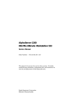
1
AlphaServer GS60E
Service Manual
Order Number: EK-GS60E-SV. A01
This manual is intended for Compaq service engineers. It
includes troubleshooting information, configuration rules, and
instructions for removal and replacement of field-replaceable
units (FRUs) for the Compaq AlphaServer GS60E system.
Compaq Computer Corporation
First Printing, February 2000
The information in this publication is subject to change without notice.
COMPAQ COMPUTER CORPORATION SHALL NOT BE LIABLE FOR TECHNICAL OR
EDITORIAL ERRORS OR OMISSIONS CONTAINED HEREIN, NOR FOR INCIDENTAL
OR CONSEQUENTIAL DAMAGES RESULTING FROM THE FURNISHING,
PERFORMANCE, OR USE OF THIS MATERIAL.
This publication contains information protected by copyright. No part of this publication may be
photocopied or reproduced in any form without prior written consent from Compaq Computer
Corporation.
The software described in this guide is furnished under a license agreement or nondisclosure
agreement. The software may be used or copied only in accordance with the terms of the
agreement.
© 2000 Compaq Computer Corporation.
All rights reserved. Printed in the U.S.A.
Computer Corporation. Alpha, AlphaServer, OpenVMS, and StorageWorks are registered in
COMPAQ, the Compaq logo, and Tru64 are copyrighted and are trademarks of Compaq the U.S
Patent and Trademark Office. Microsoft and Windows are registered trademarks of Microsoft
Corporation. UNIX is a registered trademark in the U.S. and other countries, licensed
exclusively through X/Open Company Ltd. Other product names mentioned herein may be the
trademarks of their respective companies.
FCC Notice: The equipment described in this manual generates, uses, and may emit radio
frequency energy. The equipment has been type tested and found to comply with the limits for a
Class A digital device pursuant to Part 15 of FCC rules, which are designed to provide
reasonable protection against such radio frequency interference. Operation of this equipment in
a residential area may cause interference in which case the user at his own expense will be
required to take whatever measures may be required to correct the interference. Any
modifications to this device—unless expressly approved by the manufacturer—can void the
user’s authority to operate this equipment under part 15 of the FCC rules.
Shielded Cables: If shielded cables have been supplied or specified, they must be used on the
system in order to maintain international regulatory compliance.
Warning! This is a Class A product. In a domestic environment this product may cause radio
interference in which case the user may be required to take adequate measures.
Achtung! Dieses ist ein Gerät der Funkstörgrenzwertklasse A. In Wohnbereichen können bei
Betrieb dieses Gerätes Rundfunkstörungen auftreten, in welchen Fällen der Benutzer für
entsprechende Gegenmaßnahmen verantwortlich ist.
Attention! Ceci est un produit de Classe A. Dans un environnement domestique, ce produit
risque de créer des interférences radioélectriques, il appartiendra alors à l'utilisateur de prendre
les mesures spécifiques appropriées.
Contents
Preface ........................................................................................................................xi
Chapter 1
1.1
1.2
1.3
1.4
1.5
1.6
1.7
1.8
System Overview................................................................................... 1-2
TLSB System Bus ................................................................................. 1-4
Processor Module .................................................................................. 1-6
MS7CC Memory Module ....................................................................... 1-8
KFTHA Module................................................................................... 1-10
Power Subsystem Overview ................................................................ 1-12
I/O Bus and In-Cab Storage Devices................................................... 1-14
Troubleshooting Overview .................................................................. 1-16
Chapter 2
2.1
2.2
2.3
2.4
2.5
2.6
Troubleshooting with LEDs
Operator Control Panel......................................................................... 2-2
Troubleshooting TLSB Modules............................................................ 2-6
Troubleshooting a PCI Shelf ................................................................. 2-8
Troubleshooting StorageWorks Shelves ............................................. 2-10
Troubleshooting the Power Subsystem............................................... 2-12
Troubleshooting the Cooling Subsystem............................................. 2-14
Chapter 3
3.1
3.2
3.3
3.4
3.5
3.6
3.7
Introduction
Console Display and Diagnostics
Checking Self-Test Results: Console Display ....................................... 3-2
Show Configuration Display ................................................................. 3-4
Running Diagnostics: the Test Command ............................................ 3-6
Testing the Entire System .................................................................... 3-8
Sample Test Command for a Memory Module.................................... 3-10
Identifying a Failing SIMM ................................................................ 3-12
Info Command..................................................................................... 3-14
v
Chapter 4
4.1
4.1.1
4.1.2
4.1.3
4.2
4.3
4.4
4.5
4.5.1
4.5.2
4.5.3
4.6
4.6.1
4.6.2
4.6.3
Brief Description of the TLSB Bus........................................................ 4-2
Command/Address Bus................................................................... 4-2
Data Bus ......................................................................................... 4-3
Error Checking ............................................................................... 4-3
Producing an Error Log with DECevent............................................... 4-4
Getting a Summary Error Log .............................................................. 4-5
Supported Event Types......................................................................... 4-6
Sample Error Log Entries..................................................................... 4-8
Machine Check 660 Error ............................................................... 4-8
Machine Check 620 Error ............................................................. 4-17
DWLPB Motherboard (PCIA) Adapter Error Log ........................ 4-24
Console Halt Conditions ..................................................................... 4-30
CPU Double Error Halt ................................................................ 4-30
Machine Check Logout Frames .................................................... 4-39
Machine Check Error Log............................................................. 4-42
Chapter 5
5.1
5.1.1
5.1.2
5.1.3
5.1.4
5.1.5
5.1.6
5.2
5.3
5.4
5.5
5.6
5.7
5.8
5.9
5.10
5.11
5.12
vi
DECevent Error Log
Removal and Replacement Procedures
TLSB Modules....................................................................................... 5-2
How to Replace the Only Processor ................................................ 5-2
How to Replace the Boot Processor................................................. 5-4
How to Add a New Processor or Replace a Secondary
Processor ......................................................................................... 5-8
Processor, Memory, or Terminator Module Removal and
Replacement ................................................................................. 5-12
SIMM Removal and Replacement ................................................ 5-14
I/O Cable and KFTHA Module Removal and Replacement.......... 5-18
TLSB Card Cage Removal .................................................................. 5-20
Operator Control Panel....................................................................... 5-24
CD Tray............................................................................................... 5-26
AC Distribution Box............................................................................ 5-28
Power Rack Assembly ......................................................................... 5-30
Cabinet Control Logic (CCL) Panel..................................................... 5-32
BA36R StorageWorks Shelf ................................................................ 5-34
DWLPB PCI Box ................................................................................. 5-36
Plenum Assembly................................................................................ 5-38
Cabinet Panels .................................................................................... 5-40
Cables.................................................................................................. 5-42
Appendix A
A.1
A.2
A.3
A.4
A.5
A.6
Booting LFU..........................................................................................A-2
List ........................................................................................................A-4
Update...................................................................................................A-6
Exit......................................................................................................A-10
Display and Verify Commands ...........................................................A-12
Create..................................................................................................A-14
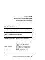
Appendix B
B.1
B.2
Updating Firmware
Console Commands and Environment Variables
Console Commands ...............................................................................B-1
Environment Variables .........................................................................B-5
Index
Examples
3–1
3–2
3–3
3–4
3–5
3–6
3–7
3–8
4–1
4–2
4–3
4–4
4–5
4–6
4–7
4–8
5–1
5–2
5–3
A–1
A–2
A–3
A–4
System Self-Test Console Display......................................................... 3-2
Show Configuration Sample ................................................................. 3-4
Sample Test Commands........................................................................ 3-6
Sample Test Command for the Entire System ..................................... 3-8
Sample Test Command, Memory Test ................................................ 3-10
Console Mode: No Failing SIMMS ...................................................... 3-12
Console Mode: Failing SIMMs Found................................................. 3-13
Examples of the Info Command.......................................................... 3-14
Producing an Error Log with DECevent............................................... 4-4
Summary Error Log .............................................................................. 4-5
OSF Event Type Identification ............................................................. 4-7
OpenVMS Event Type Identification .................................................... 4-7
Sample Machine Check 660 Error Log Entry ....................................... 4-8
Sample Machine Check 620 Error Log Entry ..................................... 4-17
Sample DWLPB Motherboad Error Log Entry ................................... 4-24
CPU Double Error Halt....................................................................... 4-33
Replacing the Only Processor Module .................................................. 5-2
Replacing the Boot Processor ................................................................ 5-4
Adding or Replacing a Secondary Processor ......................................... 5-8
Booting LFU from CD-ROM .................................................................A-2
List Command.......................................................................................A-4
Update Command .................................................................................A-6
Exit Command ....................................................................................A-10
vii
A–5
A–6
Display and Verify Commands ...........................................................A-12
Create Command ................................................................................A-14
Figures
1–1
1–2
1–3
1–4
1–5
1–6
1–7
1–8
1–9
1–10
2–1
2–2
2–3
2–4
2–5
2–6
2–7
2–8
2–9
3–1
4–1
5–1
5–2
5–3
5–4
5–5
5–6
5–7
5–8
5–9
5–10
5–11
5–12
5–13
viii
AlphaServer GS60E System ................................................................. 1-2
TLSB Card Cage ................................................................................... 1-4
Processor Module .................................................................................. 1-6
MS7CC Memory Module ....................................................................... 1-8
KFTHA Module Hoses ........................................................................ 1-10
KFTHA Module................................................................................... 1-11
GS60E Power Subsystem.................................................................... 1-12
I/O Bus and In-Cab Storage ................................................................ 1-14
Troubleshooting Steps......................................................................... 1-16
Troubleshooting Tools ......................................................................... 1-17
Operator Control Panel......................................................................... 2-2
Troubleshooting: Start with the Operator Control Panel ..................... 2-4
TLSB Module LEDs .............................................................................. 2-6
PCI Shelf ............................................................................................... 2-8
Troubleshooting Steps for PCI Shelf..................................................... 2-9
Troubleshooting StorageWorks Devices and Shelves ......................... 2-10
Power Subsystem ................................................................................ 2-12
Cooling Subsystem .............................................................................. 2-14
Cabinet Airflow ................................................................................... 2-15
Hose Numbering Scheme for KFTHA................................................... 3-5
Error Log Header Structure................................................................ 4-31
Processor, Memory, or Terminator Module ........................................ 5-12
Removing a SIMM............................................................................... 5-14
SIMM Connector Numbers – E2035 Module ...................................... 5-16
SIMM Connector Numbers – E2036 (2-Gbyte) and E2037 (4-Gbyte)
Modules ............................................................................................... 5-17
I/O Hose Cable .................................................................................... 5-18
TLSB Card Cage Removal .................................................................. 5-20
Operator Control Panel....................................................................... 5-24
CD Tray............................................................................................... 5-26
AC Distribution Box............................................................................ 5-28
Power Rack Assembly ......................................................................... 5-30
Cabinet Control Logic (CCL) Panel..................................................... 5-32
BA36R StorageWorks Shelf ................................................................ 5-34
DWLPB PCI Box ................................................................................. 5-36
5–14
5–15
5–16
Plenum Assembly................................................................................ 5-38
Cabinet Panels .................................................................................... 5-40
Cables.................................................................................................. 5-42
Tables
1
1–1
2–1
2–2
2–3
4–1
4–2
4–3
4–4
4–5
5–1
B–1
B–2
B–3
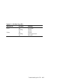
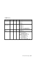
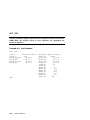
Compaq AlphaServer GS60E Documentation ....................................... xii
Memory Modules and Related SIMMs.................................................. 1-9
Operator Control Panel LEDs............................................................... 2-2
Operator Control Panel LEDs at Power-Up ......................................... 2-3
SCSI Disk Drive LEDs........................................................................ 2-11
TLSB Address Bus Commands ............................................................. 4-2
Supported Event Types......................................................................... 4-6
Parsing a Sample 660 Error (Example 4-5) .......................................... 4-8
Parsing a Sample 620 Error (Example 4-6) ........................................ 4-17
Parsing a DWLPB Motherboard Error (Example 4-7)........................ 4-24
Cables.................................................................................................. 5-43
Summary of Console Commands ..........................................................B-1
Environment Variables .........................................................................B-5
Settings for the graphics_switch Environment Variable ......................B-8
ix
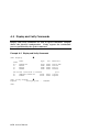
Preface
Intended Audience
This manual is written for the customer service engineer.
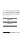
Document Structure
This manual uses a structured documentation design. Topics are organized into
small sections, usually consisting of two facing pages. Most topics begin with an
abstract that provides an overview of the section, followed by an illustration or
example. The facing page contains descriptions, procedures, and syntax
definitions.
This manual has five chapters and two appendixes.
•
Chapter 1, Introduction, introduces the AlphaServer GS60E system and
gives a brief overview of the system bus, modules, and power subsystem.
•
Chapter 2, Troubleshooting with LEDs, tells how to use the LEDs and
other indicators to find problem components in the system.
•
Chapter 3, Console Display and Diagnostics, tells how to use these
tools to find nonfunctioning components in the system.
•
Chapter 4, DECevent Error Log, describes how to interpret the error log
produced by this utility program.
•
Chapter 5, Removal and Replacement Procedures, describes the
removable and replacement procedures for GS60E components that are
replaceable by field service personnel.
•
Appendix A, Updating Firmware, describes how to use console
commands and the Loadable Firmware Update (LFU) Utility to update
system firmware.
•
Appendix B, Console Commands and Environment Variables, is a
quick reference for commands.
xi
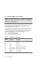
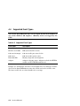
Documentation Titles
Table 1 Compaq AlphaServer GS60E Documentation
Title
Order Number
Hardware User Information and Installation
AlphaServer GS60E Installation Guide
EK–GS60E–IN
AlphaServer GS60E Operations Manual
EK–GS60E–OP
KFTHA System I/O Module Installation Card
EK–KFTHA–IN
KFE72 Installation Guide
EK–KFE72–IN
Service Information
AlphaServer GS60E Service Manual
EK–GS60E–SV
Reference Manual
AlphaServer GS60E and GS140 Getting Started with
Logical Partitions
EK–TUNLP–SF
Upgrade Manuals
GS60/8200 to GS60E Upgrade Manual
EK–GS60E–UP
H7506 Power Supply Installation Card
EK–H7506–IN
RRDCD Installation Card
EK–RRDXX–IN
Information on the Internet
Visit the Compaq Web site at www.compaq.com for service tools and more
information about the AlphaServer GS60E system.
xii
Chapter 1
Introduction
The AlphaServer GS60E system is a high-performance, symmetric multi–
processing system. It offers access to multiple high-bandwidth I/O buses, very
large memory capacities, up to eight high-performance CPUs, and many other
features normally associated with mainframe systems.
This chapter introduces the AlphaServer GS60E system. Sections in this
chapter include:
•
System Overview
•
TLSB System Bus
•
Processor Module
•
MS7CC Memory Module
•
KFTHA Module
•
Power Subsystem Overview
•
I/O Bus and In-Cab Storage Devices
•
Troubleshooting Overview
Introduction
1-1
1.1
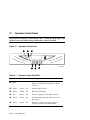
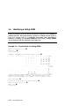
System Overview
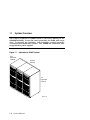
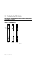
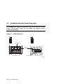
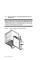
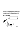
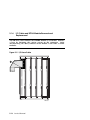
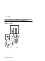
The Compaq AlphaServer GS60E system is the latest offering in the
GS60/GS140 family. It uses the same system bus, the TLSB, with seven
slots. It provides the reliability and availability features normally
associated with mainframe systems. The GS60E has redundant, hotswappable N+1 power supplies.
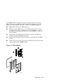
Figure 1–1 AlphaServer GS60E System
2nd
Expander
Cabinet
System
Cabinet
1st
Expander
Cabinet
SM11-99
1-2
Service Manual
AlphaServer GS60E System
The AlphaServer GS60E system main cabinet contains the seven-slot TLSB
card cage, power supplies, and space for PCI I/O shelves and StorageWorks
shelves. The GS60E system can have up to two expander cabinets (see Figure
1-1), containing additional PCI I/O shelves and StorageWorks shelves.
Chapter 2 describes how to use LEDs and other indicators to troubleshoot the
system. Chapter 3 describes the console display and diagnostics. The error log
produced by the DECevent utility program is described in Chapter 4. Removal
and replacement procedures for FRUs are described in Chapter 5.
AlphaServer GS60E Options
A list of the latest supported options is on the Internet, which you can access as
follows:
Using ftp, copy the file:
ftp://ftp.digital.com/pub/Digital/Alpha/systems/as8400/docs/supported_options.txt
Using a Web browser, follow links from the URL:
http://www.digital.com/alphaserver/products.html
Introduction
1-3
1.2
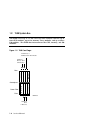
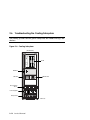
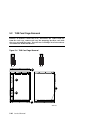
TLSB System Bus
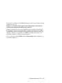
The TLSB card cage is a 7-slot card cage that contains slots for up to
four CPU modules, up to five memory array modules, and up to three
I/O modules. The TLSB bus interconnects the CPU, memory, and I/O
modules.
Figure 1–2 TLSB Card Cage
First Memory or
Additional I/O or CPU Module
Additional
Memory, I/O or
CPU Modules
4 5 6 7 8
I/O Module
Not used
Rear
Front
First CPU
Power Filter
Not used
Centerplane
3 2 1 0
OM24-99
Additional
CPUs
or Memories
1-4
Service Manual
The TLSB card cage is located in the upper part of the system cabinet. The
TLSB card cage contains seven module slots (slots 3 and 4 are not used). The
slots are numbered 0 through 2 from right to left in the front of the cabinet and
slots 5 through 8 right to left in the rear of the cabinet (see Figure 1-2). The
minimum configuration is a processor module in slot 0, an I/O module in slot 8,
a memory module in slot 7, and terminator modules in all other slots.
Module Placement Rules
Configure modules in this order:
1. Place the processor modules first. Start at slot 0 and work up to slot 2. If a
fourth processor module is used, it can be placed in slot 5, 6, or 7.
2. Place the KFTHA modules next. The first KFTHA module goes in slot 8, a
second in slot 7, and a third in slot 6.
3. Place memory modules last. The first memory module goes in the highest
numbered open slot, the next in the lowest numbered open slot, and so on,
alternating between highest- and lowest-numbered open slots.
4. Fill all remaining open slots with terminator modules.
About the TLSB Card Cage
Modules used in this system are:
Terminator
1 Gbyte memory (MS7CC-EA)
2 Gbyte memory (MS7CC-FA)
4 Gbyte memory (MS7CC-GA)
KFTHA (4 hose cables)
Dual processor (KN7CG-AB and KN7CH-AB)
The maximum number of processor modules is four.
The maximum number of memory modules is five. Memory modules may be
placed in slots 1, 2, 5, 6, and 7 only. The maximum amount of memory is 20
Gbytes. All memory modules support two-way interleaving. Mixed sizes of
memory modules may be installed in the TLSB card cage.
Each system must have a minimum of one KFTHA I/O module, installed in
slot 8.
Introduction
1-5
1.3
Processor Module
Up to four processor modules can be used in an AlphaServer GS60E
system. Each processor module contains two CPU chips.
Figure 1–3 Processor Module
1
5
3
4
2
Side 2
5
6
Side 1
SM13-99
1-6
Service Manual
The KN7CG processor module has two Alpha 21264 chips, with a clock speed of
525 MHz. The KN7CH processor module has two 21264A chips, with a clock
speed of 700 MHz. If one of the CPUs on the processor module is
malfunctioning, you replace the entire module. The chip is not a fieldreplaceable unit (FRU). The console display (see Section 3.1) shows each
processor on a module.
Figure 1-3 shows the processor module. The raised blocks in the figure
represent heatsinks that cover the chips.
➊
CPU chips. Each 21264(A) chip has a separate address and data bus for
B-cache and system operations. The 21264(A) chip has a 64-Kbyte
instruction cache and a 64-Kbyte data cache.
➋
Cache Memory. 4-Mbyte L2 cache per CPU (21264) and 8-Mbyte ECC
L2 onboard cache per CPU (21264A).
➌
TCC. The TurboLaser control chip (TCC) takes commands from both
CPUs and issues them to the TLSB. It also controls all data movements
through the TDI and SWI chips.
➍
SWIs. Two swizzle (SWI) chips receive data from the 256-bit wide DLSB
and pass it to one of the CPU chips over the 64-bit wide data interface
bus.
➎
TDIs. Four TurboLaser Data Interface (TDI) chips receive data from the
TLSB and pass the data over the DLSB to the two SWI chips.
➏
DC to DC Converters. These converters step the 48 VDC power
supplied by the power subsystem to the voltages required by the
components on the processor board.
Introduction
1-7
1.4
MS7CC Memory Module
The GS60E uses three variants of the MS7CC memory module, 1 Gbyte,
2 Gbytes, and 4 Gbytes. Up to 20 Gbytes of memory can be configured
using combinations of the three module variants.
Figure 1–4 MS7CC Memory Module
2
3
1
2
4
1
SM14-99
1-8
Service Manual
All memory modules for the AlphaServer GS60E have SIMMs (single inline
memory modules). DRAMs are mounted on small cards that are fixed to the
larger memory module by spring-held mounting clips that grip both sides of the
SIMM. Figure 1-4 shows:
➊
➋
The array of SIMMS in an MS7CC–EA (1-Gbyte) memory module.
➌
The control address interface (CTL) gate array that provides the interface
to the TLSB, controls DRAM timing and refresh, runs memory self-test,
and contains TLSB and memory-specific registers.
➍
The DC-to-DC converter.
Memory data interface (MDI) gate arrays that provide the data interface
between the TLSB bus and the DRAM arrays. The MDIs contain data
buffers, ECC checking logic, self-test data generation and checking logic,
and control and status registers (CSRs).
All types of SIMMs for all the memory modules available for AlphaServer
GS60E systems are field-replaceable. Section 3.6 describes how to isolate a
problem SIMM. When you replace a SIMM, you must be sure that the type of
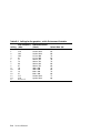
SIMM matches the module for which it is designed, as detailed in Table 1-1.
Table 1-1
Memory Modules and Related SIMMs
Memory (Size)
Motherboard
Part Number
SIMM Part Number
Number
of SIMMs
MS7CC–EA (1 GB)
EA2035-AA
54-21726-01 (32 MB)
32
MS7CC–FA (2 GB)
EA2036-AA
54-21718-01 (64 MB)
36
MS7CC–GA (4 GB)
EA2037-AA
54-24723-01 (128 MB)
36
Introduction
1-9
1.5
KFTHA Module
The KFTHA module offers four “hose” connections that interface
between the TLSB and the I/O subsystem.
Figure 1–5 KFTHA Module Hoses
Hoses
OM32-99
1-10
Service Manual
The KFTHA module is designed for high-speed, high-volume data transfers.
Direct memory access (DMA) transfers are pipelined to allow for up to 500
Mbytes/second throughput. The major elements of the KFTHA module are:
➊
RAM to buffer data for the DMA transfers.
➋
Four hose-to-data (HDP) chips, each handling 32 bits from two “hoses”
(I/O cables connecting to an adapter in an associated I/O bus). Data on
the HDPs flow in one direction; either “up” (to the KFTHA) or “down” (to
the I/O adapter).
➌
Four I/O data path (IDP) chips, which together handle a 256-bit data
transfer to or from the TLSB system bus.
➍
An I/O control chip (ICC) houses the primary control logic for the TLSB
interface.
➎
A DC-to-DC converter that converts the 48 VDC system power to the DC
voltage required by the KFTHA module.
Figure 1–6 KFTHA Module
2
3
1
4
3
5
SM16-99
Introduction
1-11
1.6
Power Subsystem Overview
The power subsystem consists of an AC input box, a DC distribution
module, redundant hot swap power supplies, a cabinet control logic
(CCL) panel, and cables.
Figure 1–7 GS60E Power Subsystem
Front
Rear
CCL Panel
DC Distribution
Module
Power
Supplies
Power
Supplies
AC Input Box
GS60E23-99
1-12
Service Manual
Three-phase AC power enters the system by cable through the AC input box
(see Figure 1-7). The H7506 power supplies convert three-phase AC power to 48
VDC. Three hot-swappable power supplies offer n+1 redundancy; that is, if any
one power supply fails, the remaining two supply the needed power.
Introduction
1-13
1.7
I/O Bus and In-Cab Storage Devices
Both the AlphaServer GS60E main cabinet and expander cabinets are
designed to hold PCI shelves and StorageWorks I/O shelves.
Figure 1–8 I/O Bus and In-Cab Storage
(Front View)
(Rear View)
7-Slot System Bus
Up to 4 CPU Modules
(8 CPUs)
Up to 5 Memory Modules
(12 GB)
Up to 3 I/O Modules
Blowers
DWLPB PCI
CD Drive
(and optional
floppy drive)
StorageWorks
Shelf
Power Supplies
CCL Panel
AC Input Box
SM18-99
1-14
Service Manual
Figure 1-8 shows an AlphaServer GS60E system cabinet.
As shown, PCI shelves and StorageWorks shelves are mounted horizontally.
Each StorageWorks shelf has room for up to seven devices, including a signal
converter and 3.25-inch disks or tapes. A power unit (DC-to-DC converter) is in
the leftmost slot of shelf.
The system cabinet has space for up to two PCI shelves (DWLPB-DA) and three
StorageWorks shelves (BA36R-RC/RD UltraSCSI).
Each expander cabinet has space for four PCI shelves and three StorageWorks
shelves or three PCI shelves and four StorageWorks shelves.
Introduction
1-15
1.8
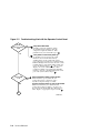
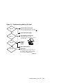
Troubleshooting Overview
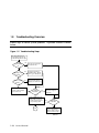
Follow steps to isolate system problems. A possible routine is shown
below.
Figure 1–9 Troubleshooting Steps
You cannot find cause of
user problem by phone. Go
to site and follow these steps.
Control
panel LEDs
lit
No
Check power subsystem
(see Section 2.5)
Yes
Yes
Operating system
running
Customer experiences
intermittent error: Check
error log (see Chapter 4)
No
Console software
running
Yes
Type "init" command.
Check system self-test
display (see Section 3.1)
No
Restart system. Check
system self-test display
(see Section 3.1)
Identify
faulty FRU
No
Boot operating system,
check error log (see
Chapter 4)
Yes
Power down system and
replace FRU. Power up.
If system self-test passes,
boot operating system.
Yes
Identify
faulty FRU
No
Done
Problem is beyond the
scope of this Service
Manual. Call customer
support center for help.
SM19-99
1-16
Service Manual
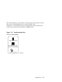
The system hardware, console software, and operating system software provide
three types of troubleshooting tools, as shown in Figure 1-10.
Chapters 2, 3, and 4 tell how to use these tools to isolate faulty components or
report software problems for AlphaServer GS60E systems.
Figure 1-10
Troubleshooting Tools
Tools for Finding Problems
LEDs and Indicators
System Self-Test and
Other Console Displays
Error Log Printout
SM110-99
Introduction
1-17
Chapter 2
Troubleshooting with LEDs
This chapter tells how to use the LED displays and other indicators to track
down faulty components that you can replace in the AlphaServer GS60E
system.
LEDs give status on the power subsystem, system bus (TLSB) modules
(processor, memory, and I/O) the I/O bus, and devices in shelves. The cooling
subsystem consists of two blowers located in the center of the system cabinet.
They can be checked by looking and listening for the fans.
Sections in this chapter are as follows:
•
Operator Control Panel
•
Troubleshooting TLSB Modules
•
Troubleshooting a PCI Shelf
•
Troubleshooting StorageWorks Shelves
•
Troubleshooting the Power Subsystem
•
Troubleshooting the Cooling Subsystem
Troubleshooting with LEDs
2-1
2.1
Operator Control Panel
Start with the operator control panel (OCP). Check the OCP lights. The
OCP has six status LEDs, three pushbuttons, and a keyswitch.
Figure 2–1 Operator Control Panel
1
2
3
4
5
6
OM29-99
Table 2–1 Operator Control Panel LEDs
Light
Color
State
Meaning
➊ – Run
Green
On
Power is supplied to entire system; the
blowers are running. System has exited
console.
➋ – Power
Green
On
System is powered on.
➌ – Fault
Yellow
On
Fault on system bus.
➍ – On
Green
On
Power is supplied to the whole system.
➎ – Secure
Green
On
Indicates input from the console device is
prevented.
➏ – Reset
Yellow
On
Indicates a system reset has occurred,
clearing captured error information.
2-2
Service Manual
Six status indicator LEDs (see Figure 2-1) show the state of the system. Table
2-1 describes the conditions indicated by the lights.
NOTE: With the keyswitch in the On position, if all six LEDs are blinking, one
or more of the power supplies has failed or there is a missing power
supply. With the keyswitch in the Off position, the LEDs will also blink
but do not provide power supply status.
Table 2–2 Operator Control Panel LEDs at Power-Up
Action
Set circuit
breaker to On
Turn
keyswitch to
On and press
On button
System selftest starts
Module
passes selftest
Module fails
self-test
Power supply
problem
Operating
system boots
Keyswitch
On; On/Off
Button On
Run
Power
Fault
On
Secure Reset
Off
Blink
Blink
Blink
Blink
Blink
Blink
On
Off
On
Blink
On
Off
Off
On
Off
On
On
On
Off
Off
On
Off
On
Off
On
Off
Off
On
Off
On
On
On
Off
Off
On
Blink
Blink
Blink
Blink
Blink
Blink
On
On
On
Off
On
Off
Off
Troubleshooting with LEDs
2-3
Figure 2-2
Troubleshooting: Start with the Operator Control Panel
On/Off
button/ keyswitch
is Off
Yes
1
No
2
Fault LED
is lit
3
Yes
No
Fix problem identified.
If a faulty component or firmware update
was identified as the problem, replace the
component or update the firmware. If the
problem has not yet been identified, go to 2
Turn power on and watch power-up.
As 48-VDC power is passed to the system,
initial tests are run on the CPU, memory,
and I/O adapters on the system. If the system
passes this power-up testing, the green Run and On
LEDs should light. If it does not, look at the console
terminal display to pinpoint the failing module and
replace the module. Repeat 2 . ( If no console
display, the console terminal may be a TGA
(graphics) terminal, connected through a PCI bus.
Connect a character-cell terminal through the serial
port on the system cabinet. Repeat 2
Some component failed system self-test.
If Run and On are green, Fault is lit, and
system self-tests have completed, replace
any failed component and proceed with 2
System clock and CPUs are not synchronized.
If Run is off and On is green, Fault is lit, and
system self-test did not complete, check to see if
the system clock and the CPUs have different cycle
times. Replace as appropriate and proceed with 2
A
SM22-99
2-4
Service Manual
Figure 2-2
Troubleshooting: Start with the Operator Control Panel
(Continued)
A
Any LEDs lit
on control panel
No
4
Yes
Green LED(s)
lit
Yes
5
Status LEDs are not receiving power/signals.
Check the power supplies to see if DC power is
leaving the supply. If so, check the power and
signal lines to the CCL panel. Check the cabling between
the CCL and the operator control panel. If connections
seem OK, replace CCL. If still no lights on control
panel, replace control panel. Proceed with 2
System self-test passed (On is lit);
operating system running (Run is lit).
If both green LEDs are lit, system self-test has
passed, and the operating system is running. Check
the error log (see Chapter 4). Ensure that the
proper boot disk is selected to boot the operating system.
If Run is not lit, boot the operating system.
When the operating system boots, look at the error log.
SM22B-99
Troubleshooting with LEDs
2-5
2.2
Troubleshooting TLSB Modules
You can check individual module self-test results by looking at the
status LEDs on the module.
Figure 2–3 TLSB Module LEDs
LEDs
CPU
Memory
KFTHA
SM24-99
2-6
Service Manual
In general, if a module on the TLSB does not pass self-test (green light is not lit)
it should be replaced.
There is a case where some removal and replacement action may be
needed even though the module passes self-test.
Failure of the built-in self-test for the MS7CC modules indicates that testing
has shown that there is no single 64-Kbyte segment of memory that is usable.
Each 64-Kbyte segment must show at least 256 bad pages before it is noted as
unusable. However, it is possible for a SIMM to warrant replacement, even
though the module as a whole passes its self-test.
You can determine faulty SIMMs with the show config console command, as
described in Chapter 3.
Troubleshooting with LEDs
2-7
2.3
Troubleshooting a PCI Shelf
LEDs show the status of the power supplies, as well as the adapter selftest results in the PCI shelf.
Figure 2–4 PCI Shelf
1
2
3
4
DWLPB LED numbers
OM55-99
LED Status in PCI Shelf
LED 1 - On-board power system OK
LED 2 - Motherboard self-test passed
LED 3 - 48 VDC power supply OK
LED 4 - Hose Error
2-8
Service Manual
Figure 2-5
Troubleshooting Steps for PCI Shelf
LED 3 lit
No
Yes
No
LED 1 lit
11
Check Cabling to PCI shelf.
Check to make sure the clip connectors
are engaged properly. If so, proceed to 2
2
Check 48V Power Supply.
13 Internal Power System Error.
Check fans in blower; check
for jumper cable (a small plug) replacing
fan connection.
Yes
3
LED 2 lit
No
Power
Board.
Yes
15 Replace Motherboard.
Yes
LED 4 lit
4 Replace
16 Hose Error.
Some error has occurred in the protocol
governing the transfer of data over the
hose. Replace the hose first, the motherboard second, the KFTHA third.
OM56-99
Troubleshooting with LEDs
2-9
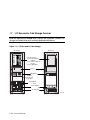
2.4
Troubleshooting StorageWorks Shelves
StorageWorks devices are mounted in horizontal shelves in the GS60E
system or expander cabinet. LEDs are located on each disk drive.
Figure 2–6 Troubleshooting StorageWorks Devices and Shelves
Green LEDs
Yellow LEDs
OM57-99
2-10
Service Manual
Table 2-3 SCSI Disk Drive LEDs
Indicator LED
LED State
Meaning
Green
Off
Flashing
On
No activity
Activity
Activity
Yellow
Off
Flashing
On
Normal
Spin up/spin down
Not used
Troubleshooting with LEDs
2-11
2.5
Troubleshooting the Power Subsystem
The GS60E power supplies accept three-phase AC and produce 48 VDC
power.
Each power supply has two LEDs that indicate normal
conditions and faults.
Figure 2–7 Power Subsystem
Front
VAUX LED (top)
Rear
Power
Supplies
48V LED (bottom)
AC Power Line Cord
Main Circuit Breaker
SM27-99
2-12
Service Manual
The system must be provided with a suitable source of 3-phase AC power.
Three H7506 power supplies (see Figure 2-7) provide the necessary power and
power redundancy required for all internal system components.
The AC input box is located at the bottom of the system cabinet (when viewing
the system cabinet from the rear). The 48 VDC power supplies are located
above the AC input box and are visible when viewing the system cabinet from
the front.
The AC input box provides the interface for the system to the AC utility power.
The DC distribution module connects the AC input box and power supplies. It
distributes the 48 VDC power. The circuit breaker and power indicators are at
the rear of the cabinet.
Circuit Breaker
The main circuit breaker, CB1, controls power to the entire system, including
the power supplies, blowers, and in-cabinet options. Current overload causes
the breaker to trip to the Off position, so that power to the system is turned off.
For normal operation, circuit breaker CB1 must be in the On position, with the
handle pushed up. To shut the circuit breaker off, push the handle down. Subbreakers CB2 through CB11 should also be in the On (up) position during
normal system operation.
AC Power Indicators
Three lights above the AC power line cord (see Figure 2-7) indicate that AC
power is supplied to the line side of main circuit breaker CB1.
The power supplies have two LEDs that indicate normal conditions and faults.
When the system (keyswitch) is off, plugged in, and the circuit breakers are on,
power is present only within the AC box and power supplies. The green VAUX
LEDs on the power supplies should be illuminated. When the system is on, the
VAUX and 48V LEDs should light.
Troubleshooting with LEDs
2-13
2.6
Troubleshooting the Cooling Subsystem
The cooling system cools the power subsystem, the TLSB card cage, and
shelves.
Figure 2–8 Cooling Subsystem
(Front View)
TLSB
Blowers
CD Drive
DWLPB PCI
StorageWorks
Shelf
Power Supplies
AC Input Box
SM28-99
2-14
Service Manual
The cooling system is designed to keep the system components at an optimal
operating temperature. It is important to keep the front and rear doors free of
obstructions, leaving a minimum clearance space of 1.5 meters (59 inches) in
the front and 1 meter in the rear to maximize airflow.
Two blowers, located in the center of the cabinet (see Figure 2-8) draw air
downward through the TLSB card cage. Air is exhausted at the middle of the
cabinet, to the rear (see Figure 2-9). The blower speed varies based on the
system’s ambient temperature.
CAUTION: Anything placed on the top of the cabinet could restrict airflow.
This will cause the system to power down.
Figure 2-9 Cabinet Airflow
OM211-99
Troubleshooting with LEDs
2-15
Chapter 3
Console Display and Diagnostics
This chapter describes how hardware diagnostic programs are executed when
the system is initialized. Sections include:
•
Checking Self-Test Results: Console Display
•
Show Configuration Display
•
Running Diagnostics: the Test Command
•
Testing the Entire System
•
Sample Test Command for a Memory Module
•
Identifying a Failing SIMM
•
Info Command
Console Display and Diagnostics
3-1
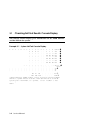
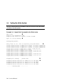
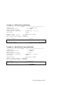
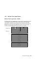
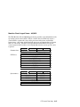
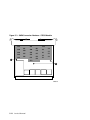
3.1
Checking Self-Test Results: Console Display
The self-test console display gives information for the TLSB modules
and the PCIs in the system.
Example 3–1 System Self-Test Console Display
F
E
D
C
B
A
+
.
.
.
.
.
.
.
.
.
.
.
.
.
.
.
.
.
.
9
+
.
.
.
8
7
6
5
4
3
2
1
0
NODE #
A
M
M
M
.
.
P
P
P
TYP
o
+
+
+
.
.
++
++
++
ST1
.
.
.
.
.
.
EE
EE
EB
BPD
o
+
+
+
.
.
++
++
++
ST2
.
.
.
.
.
.
EE
EE
EB
BPD
o
+
+
+
.
.
++
++
++
ST3
.
.
.
.
.
.
EE
EE
EB
BPD
+
.
.
.
.
+
.
.
.
.
+
.
.
.
.
+
.
.
.
.
+
.
.
.
.
B0
A1
A0
.
.
.
.
.
.
.
.
.
.
.
.
.
. +
.
.
.
.
.
.
.
.
.
.
C0 PCI +➒
EISA +
C1 ➓
C2
C3
ILV
➀
. 4GB 4GB 4GB .
. . . .
12GB ➁
Compaq AlphaServer GS60E2-6/700/8, Console V5.5-25 26-OCT-1999 12:06:03
SROM V2.3, OpenVMS PALcode V1.68-101, Tru64 UNIX PALcode V1.61-101 ➂
System Serial = NI84177052, OS = OpenVMS, 3:11:57 December 7, 1999
:
:
P00>>>
3-2
Service Manual
➊
➋
➌
➍
➎
➏
➐
➑
➊
➋
The NODE # line lists the node numbers on the TLSB and I/O buses.
The TYP line in the printout indicates the type of module at each TLSB
node. Processors are type P, memories are type M, and the KFTHA port
module is type A. A period (.) indicates that the slot is not populated or that
the module is not reporting.
➌ This line shows the results of individual processor and memory module tests.
Possible values are pass (+) or (–). Since the I/O port module does not have a
module-resident self-test, its entry for the ST1 line is always "o".
➍ The BPD line indicates boot processor determination. When the system goes
through self-test, the processor with the lowest ID number that passes selftest (ST1 line is +) becomes the boot processor, unless you intervene. The
process occurs again after ST2 and ST3 testing. “B” indicates boot processor,
“E” indicates the processor is enabled to become the boot processor, and “D”
indicates that a console command has been issued disabling the processor
from the possibility of becoming the boot processor.
This BPD line is printed three times. After the first determination of the
boot processor, the processors go through two more rounds of testing. Since it
is possible for a processor to pass self-test (at line ST1) and fail ST2 or ST3
testing, the processors again determine the boot processor following each
round of tests. The first processor to pass self-test is chosen as the boot
processor.
➎ During the second round of testing (ST2) all processors run additional CPU
tests involving memory.
➐ During the third round of testing (ST3) all processors run multiprocessor
tests, and the status of each processor is once again reported on the BPD line.
➑ The primary CPU also tests the I/O port module at this time.
➒ In Example 3-1, the PCI (channel C0) and its options at nodes 0, 5, 6,
7, 8, 9, 10, and 11 passed self-test as indicated by the + symbols.
➓ I/O channels C1, C2, and C3 are not used.
➀ The ILV line contains a memory interleave value (ILV) for each memory.
➁ This line displays the size of each memory module and gives the total
size of system memory. In Example 3-1, the total size is 12 Gbytes.
➂ Console version and firmware revision date are given.
Console Display and Diagnostics
3-3
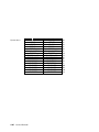
3.2
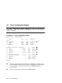
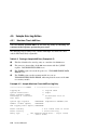
Show Configuration Display
The show configuration console command is useful to obtain more
information about the system configuration, in case you need to
replace a module.
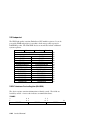
Example 3–2 Show Configuration Sample
P00>>> show configuration
Name
TLSB
0++ KN7CG-AB
6+ MS7CC
7+ KFTHA
8+ KFTHA
Type
Rev
Mnemonic
8025
5000
2020
2000
0000
0000
0000
0000
kn7cg-ab0 ➊
ms7cc0
kftha0
kftha1
C0 PCI connected to kftha0
0+ SIO
4828086
7+ KZPSA
8101
8+ ISP1020
8101
A+ DAC960
11069
Controllers on SIO
0+ DECchip 21040-AA
1+ FLOPPY
2+ KBD
3+ MOUSE
21011
2
3
4
0003
0000
0000
0000
0000
0000
0000
0000
pci0
sio0
kzpsa0
kzpsa1
dac0
➋
➌
➍
➎
sio0
➏
tulip0
floppy0
kbd0
mouse0
P00>>>
➊
The first grouping shows the modules on the TLSB bus and their status.
In this example, the processor is in slot 0, as shown in the console display
of system self-test. A memory is at node 6, and KFTHA modules at
nodes 7 and 8.
➋
C0 is next, showing the PCI bus on the KFTHA module.
3-4
Service Manual
➌
➍
➎
➏
Node 0 is the KFE72 standard I/O PCI/EISA adapter module.
Nodes 7 and 8 are the KZPSA adapters.
This line shows the DA960 controller.
These lines show the controllers on the SIO module.
Figure 3-1 shows the connector numbering scheme for the KFTHA module.
Each slot has four connector numbers associated with it, numbered in
increasing order from top to bottom, as shown.
Figure 3–1 Hose Numbering Scheme for KFTHA
Centerplane
C0 C4
C8
C3
C7
C11
8
7
6
5
4
TLSB node
SM31-99
Console Display and Diagnostics
3-5
3.3
Running Diagnostics: the Test Command
The test command allows you to run diagnostics on the entire system,
an I/O subsystem, a single module, a group of devices, or a single
device.
Example 3–3 Sample Test Commands
P00>>> test
# Tests the entire system.
# Default run time is 10 minutes.
P00>>> t pci0 –t 60
# Tests all devices associated
# with the PCI0 subsystem. Test
# run time is 60 seconds.
P00>>> test ms*
# Tests all ms7cc memory modules.
P00>>> t –q
# Status messages will not be
# displayed during test time.
3-6
Service Manual
You enter the command test to test the entire system using exercisers resident
in ROM on the boot processor module. No module self-tests are executed when
the test command is issued without a mnemonic.
When you specify a subsystem mnemonic or a device mnemonic with test, such
as test pci0 or test ms7cc0, self-tests are executed on the associated modules
first and then the appropriate exercisers are run.
Console Display and Diagnostics
3-7
3.4
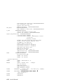
Testing the Entire System
The test command with no modifiers runs all exercisers for subsystems
and devices on the system.
Example 3–4 Sample Test Command for the Entire System
P00>>>test
➊
Console is in diagnostic mode
Complete Test Suite for runtime of 1200 seconds
Type ^C to stop testing
➋
Configuring system...
:
:
Memory Tests not run.
Starting
Starting
Starting
Starting
Starting
Stopping
Starting
Stopping
Starting
Stopping
Starting
Stopping
Starting
Stopping
Must run separately using TEST MS7CC*
network exerciser on ewa0.0.0.12.0 (id #28f) in internal loopback
network exerciser on ewb0.0.0.11.0 (id #2a1) in internal loopback
network exerciser on ewc0.0.0.12.4 (id #2b3) in internal loopback
network exerciser on ewd0.0.0.11.4 (id #2c5) in internal loopback
device exerciser on dka0.0.0.4.0 (id #36f) in READ-ONLY mode
device exerciser on dka0.0.0.4.0 (id #36f)
device exerciser on dka100.1.0.4.0 (id #5df) in READ-ONLY mode
device exerciser on dka100.1.0.4.0 (id #5df)
device exerciser on dka200.2.0.4.0 (id #858) in READ-ONLY mode
device exerciser on dka200.2.0.4.0 (id #858)
device exerciser on dka300.3.0.4.0 (id #acc) in READ-ONLY mode
device exerciser on dka300.3.0.4.0 (id #acc)
device exerciser on dka400.4.0.4.0 (id #d37) in READ-ONLY mode
device exerciser on dka400.4.0.4.0 (id #d37)
Stopping all testing...
Stopping
Stopping
Stopping
Stopping
network
network
network
network
exerciser
exerciser
exerciser
exerciser
on
on
on
on
ewd0.0.0.11.4
ewc0.0.0.12.4
ewb0.0.0.11.0
ewa0.0.0.12.0
---------Testing done ------------
3-8
Service Manual
➍
please wait
(id
(id
(id
(id
#2c5) ➎
#2b3)
#2a1)
#28f)
➌
mode
mode
mode
mode
Example 3–4 Sample Test Command, System Test (Continued)
Shutting
Shutting
Shutting
Shutting
Shutting
Shutting
Shutting
Shutting
Shutting
Shutting
Shutting
Shutting
Shutting
Shutting
Shutting
Shutting
:
:
P00>>>
down
down
down
down
down
down
down
down
down
down
down
down
down
down
down
down
drivers...
units on tulip2, slot 12, bus 0, hose 4...
units on floppy1, slot 0, bus 1, hose 4...
units on isp4, slot 6, bus 0, hose 4...
units on isp5, slot 7, bus 0, hose 4...
units on isp6, slot 8, bus 0, hose 4...
units on isp7, slot 9, bus 0, hose 4...
units on isp8, slot 10, bus 0, hose 4...
units on tulip3, slot 11, bus 0, hose 4...
units on tulip0, slot 12, bus 0, hose 0...
units on floppy0, slot 0, bus 1, hose 0...
units on isp0, slot 4, bus 0, hose 0...
units on isp1, slot 6, bus 0, hose 0...
units on isp2, slot 7, bus 0, hose 0...
units on isp3, slot 8, bus 0, hose 0...
units on tulip1, slot 11, bus 0, hose 0...
➏
➊ In Example 3-4, the operator enters the test command. The
complete test suite runs for 1200 seconds.
➋ To stop execution of the test command before normal completion,
use Ctrl/C (^C). Termination using ^C may take a number of
seconds depending upon the particular configuration being tested.
➌ Memory testing is done separately. Status messages indicate the
start of the console-based exercisers.
➍ Testing is complete.
➎ All exercisers are stopped, as indicated by the status messages.
➏ The console prompt returns.
Console Display and Diagnostics
3-9
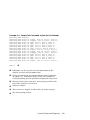
3.5
Sample Test Command for a Memory Module
To test a processor, memory module, or an I/O adapter and its
associated devices, enter the test command and the correct mnemonic.
Mnemonics are displayed when you enter a show configuration or a
show device command.
Example 3–5 Sample Test Command, Memory Test
P00>>> set d_report full
➊
P00>>> test ms*
Console is in diagnostic mode
Memory subsystem test selected for runtime of 1200 seconds
Type Ctrl/C to abort...
**************************************************************
*
*
* ALLOW AT LEAST 2 MINUTES OF TESTING TIME FOR EACH GIGABYTE *
*
OF MAIN MEMORY
*
*
*
*
SINGLE-BIT ERROR REPORTING IS ENABLED
*
*
*
**************************************************************
Starting Cache Coherency Tests
Starting Marching 1’s and 0’s Tests
Memory size is 8192 MB
More than 2 GB memory present ... memory size is 1FFE
Starting Victimize Tests
>2 GB memory testing beginning ...
Starting test 4 at addresses 7F400000 and 10F800000
Starting test 2 at addresses 13F900000 and 16FA00000
Starting test 2 at addresses AF500000 and 19FB00000
Still testing Memory...
Still testing Memory...
Still testing Memory...
:
:
Still testing Memory...
Still testing Memory...
Stopping all testing... please wait
---------Testing done ------------
3-10
Service Manual
Example 3–5
Shutting
Shutting
Shutting
Shutting
Shutting
Shutting
Shutting
Shutting
Shutting
Shutting
Shutting
Shutting
:
:
P00>>>
down
down
down
down
down
down
down
down
down
down
down
down
Sample Test Command, Memory Test (Continued)
drivers...
units on tulip2, slot 12, bus 0, hose 4...
units on floppy1, slot 0, bus 1, hose 4...
units on isp4, slot 6, bus 0, hose 4...
units on isp5, slot 7, bus 0, hose 4...
units on isp6, slot 8, bus 0, hose 4...
units on isp7, slot 9, bus 0, hose 4...
units on isp8, slot 10, bus 0, hose 4...
units on tulip3, slot 11, bus 0, hose 4...
units on tulip0, slot 12, bus 0, hose 0...
units on floppy0, slot 0, bus 1, hose 0...
units on isp0, slot 4, bus 0, hose 0...
In Example 3-5:
➊ Enter test ms*.
➋ All MS7CC memory modules are tested by the memory exerciser, a
series of tests executed from the processor module.
NOTE: To test a single memory module on your system, type:
test ms7ccn, where n is the module number.
Console Display and Diagnostics
3-11
3.6
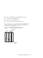
Identifying a Failing SIMM
From the console, you can check for flawed or poorly seated SIMMs in
memory boards. This information is useful as a simple on-site check as
part of a service call, as a validation procedure after upgrading a
memory, or adding or changing SIMMs for any reason. Failing SIMMs
are also reported in the error log (see Chapter 4).
Example 3–6 Console Mode: No Failing SIMMS
➊
P00>>> set simm_callout on
P00>>> init ➋
Initializing…. . .
WARNING:
F
E
D
C
B
A
+
.
.
.
.
.
.
.
.
.
➌
SIMM_CALLOUT environment variable is ON
.
.
.
.
.
.
9
+
.
.
.
8
A
o
.
o
.
o
.
7
M
+
.
+
.
+
.
+
.
.
.
+
.
.
.
.
6
M
+
.
+
.
+
.
+
.
.
.
.
5
M
+
.
+
.
+
.
+
.
.
.
.
4
.
.
.
.
.
.
.
+
.
.
.
.
3
.
.
.
.
.
.
.
.
.
.
.
.
2
P
++
EE
++
EE
++
EE
.
.
.
.
.
1
P
++
EE
++
EE
++
EE
.
.
.
.
.
0
P
++
EB
++
EB
++
EB
.
.
.
.
.
+
.
.
.
NODE #
TYP
ST1
BPD
ST2
BPD
ST3
BPD
C0 PCI +
EISA +
C1
C2
C3
B0 A1
A0
.
.
. . . ILV
. 4GB 4GB 4GB .
. . . .
12GB
Compaq AlphaServer GS60E2-6/700/8, Console V5.5-25 26-OCT-1999 12:06:03
SROM V2.3, OpenVMS PALcode V1.68-101, Tru64 UNIX PALcode V1.61-101
System Serial = NI84177052, OS = OpenVMS, 3:11:57 December 7, 1999
:
P00>>> show simm ➍
No selftest errors found on any memory modules!
P00>>> set simm_callout off
P00>>> init ➐
Initializing. . .
3-12
Service Manual
➏
➎
➊
The set simm_callout on command sets an internal environment
variable that enables code that isolates failing SIMMs during memory
testing. With this variable enabled, system self-test can take up to 40
seconds longer if a faulty SIMM is present.
➋
The init command initializes the system and prints the console map.
➌
This line in the console display notes that the SIMM callout
environment variable is on.
➍
The show simm command requests a display of faulty SIMMS.
➎
➏
In Example 3-6, no faulty SIMMs were found.
➐
The set simm callout off command turns off the environment
variable that enabled callout of faulty SIMMs.
The init command initializes the system in normal mode.
Example 3-7 shows a show simm command that calls out some failing SIMMs.
Section 5.1.5 tells how to locate, remove, and replace SIMMs in a memory
module.
Example 3-7 Console Mode: Failing SIMMS Found
.
. ➊
.
P01>>> show simm ➋
The following SIMMs are faulty on memory module in slot 7
J30
J31
➌
➊
The set simm_callout on and init commands are omitted here for
brevity.
➋
The show simm command requests a display of faulty SIMMs.
➌
SIMMS numbered J30 and J31 on the memory module in slot 7 are found
to be faulty.
Console Display and Diagnostics
3-13
3.7
Info Command
The info command provides information useful in debugging the
system. Some of the information it provides can be useful for isolating
FRUs in the field.
Example 3–8 Examples of the Info Command
P00>>> info ➊
0. About the console
➋
1. Bitmap
2. PAL symbols
3. IMPURE area (abbreviated)
4. IMPURE area (full)
5. TLSB Registers
6. GBUS
7. LOGOUT area
8. Per Cpu HWRPB areas ➋
9. LAMB registers
10. TLSB register addresses
11. Page Tables
12. FRU table ➋
13. Console internals
14. Supported devices
15. Console SCB
16. PCIA
Enter selection: 5 ➌
Node0
Node1
Node 7
Node8
KN7CG-AB
MS7CC
MS7CC
KFTHA
Base adr 88000000 88800000 89c00000 8a000000
TLDEV
00005000 00008014 00002020 00002000
TLBER
00100000 00800000 00000000 00000000
TLCNR
000fc200 00000220 00000170 00000180
TLVID
00000080 00000054
TLMMR0
00008014 80000010 80000010
TLMMR1
00008014 00000000 00000000
TLMMR2
00008014 00000000 00000000
TLMMR3
00008014 00000000 00000000
TLMMR4
00008014 00000000 00000000
TLMMR5
00008014 00000000 00000000
TLMMR6
00008014 00000000 00000000
TLMMR7
00008014 00000000 00000000
3-14
Service Manual
➍
TLFADR0
TLFADR1
TLESR0
TLESR1
TLESR2
TLESR3
TLILID0
0011ab00
07050000
00000303
00000c0c
00006060
00009090
00400303
00400c0c
00406060
00409090
Node0
KN7CG-AB
Node1
MS7CC
00000000 00000000
00000000 00000000
00000000 00000000
00000000 00000000
00000000 00000000
00000000 00000000
00000000 00000000
Node 7
Node8
MS7CC
KFTHA
00000000 00000000
00000000 00000000
00000000 00000000
00000010 00000010
TLILID1
TLILID2
TLILID3
TLCPUMASK
.
.
.
P00>>> info 5 | grep TLBER ➎
TLBER
00100000 00800000 00000000
P00>>> info 5 | grep TLMMR* ➏
TLMMR0
00008014 80000010
TLMMR1
00008014 00000000
TLMMR2
00008014 00000000
TLMMR3
00008014 00000000
TLMMR4
00008014 00000000
TLMMR5
00008014 00000000
TLMMR6
00008014 00000000
TLMMR7
00008014 00000000
P00>>>
00000000
80000010
00000000
00000000
00000000
00000000
00000000
00000000
00000000
➊
The info command lists options available. (This list may change.)
➋
The bitmap, HWRPB, and FRU table options only provide relevant
information after the operating system has been running and halted with
Ctrl/P to return to console mode.
➌
The user enters the selection 5 for a listing of TLSB registers.
➍
The listing of bus registers continues for several pages; this is only the first
page and a half to show that bus registers for all the modules are listed.
➎
The console commands allow the UNIX concept of “piping.” Here, an info
command requesting a listing of TLSB registers is piped into a grep
command, which prints all lines produced by the info 5 that contain
TLBER.
➏
This is another example of UNIX-type piping, showing the grep command
with a “wildcard” (*), in which all lines produced by the info 5 command
beginning with TLMMR are printed.
Console Display and Diagnostics
3-15
Chapter 4
DECevent Error Log
This chapter discusses error logs produced by the DECevent bit-to-text
translator. Sections include:
•
Brief Description of the TLSB Bus
•
Producing an Error Log with DECevent
•
Getting a Summary Error Log
•
Supported Event Types
•
Sample Error Log Entries
•
Console Halt Conditions
DECevent Error Log
4-1
4.1
Brief Description of the TLSB Bus
The error log entries discussed here are specific to the AlphaServer
GS60E system. Most of the errors occur during the transmission of
commands or data along the TLSB system bus or in buses or storage
internal to a particular module.
To understand some of the terms used in the error log, you should understand
how data is transferred on the TLSB system bus. The TLSB has two separate
buses: a command/address bus and a data bus. Thus, errors can refer to
transmissions on either of these buses.
A node that initiates a transaction is called a commander node. The node that
responds to the command issued by the commander is called the slave node.
CPUs or I/O nodes are always the commander on memory transactions and can
be either the commander or the slave on CSR (control and status register)
transactions. Memory nodes are never commander nodes.
4.1.1
Command/Address Bus
Table 4-1 lists the eight address bus commands.
Table 4–1 TLSB Address Bus Commands
TLSB CMD
<2:0>
Command
Description
000
No-op
Device that won arbitration nulled the
command
001
Victim
Victim
010
Read
Read memory
011
Write
Memory write or write update
100
Read Bank Lock
Read memory bank, lock
101
Write Bank Lock
Write memory bank, unlock
110
CSR Read
Read CSR data
111
CSR Write
Write CSR data
4-2
Service Manual
4.1.2
Data Bus
The TSLB transfers data in the sequence order that valid address bus
commands are issued. In addition to 256 bits of data, the data bus contains
associated ECC bits and some control signals. Three signals are of particular
significance in read and write operations.
TLSB_SHARED – When a request is made to access memory, each CPU notes
whether the block of memory is currently resident in cache, and, if so, asserts a
signal that the data is shared. Thus, when the slave responds with the data, it
asserts the TLSB_SHARED signal on the data bus, so that CPU nodes can take
note and make sure that the block being accessed remains valid in the CPU’s
cache. This signal is valid when driven in response to Read, Read Bank Lock,
Write, and Write Bank Unlock commands.
TLSB_DIRTY – This signal is used to indicate that the block being accessed is
valid in a CPU cache, and that the copy there is more recent than the copy in
memory. TLSB_DIRTY is guaranteed to be valid in response to Read and Read
Bank Lock commands.
TLSB_STACHK – This signal is asserted whenever TLSB_SHARED or
TLSB_DIRTY are asserted, to ensure that, should an error occur in
transmission or reception of either one of these signals, it can be detected. For
example, if TLSB_SHARED or TLSB_DIRTY is asserted, but TLSB_STACHK is
not, there is an error. Or, if TLSB_STACHK is asserted and TLSB_SHARED or
TLSB_DIRTY is not, there is also an error.
4.1.3
Error Checking
The TLSB is designed to implement error detection and, where possible, error
correction. The TLSB uses parity protection on the address bus. The data bus
is protected by ECC (error correction code). Protocol sequence checking is used
on the control signals across both buses. Cache coherency is monitored with the
use of the TLSB_SHARED and TLSB_DIRTY signals described above.
PALcode collects error information from module control and status registers and
formats it into a “logout frame” that is passed to the operating system, which
uses the information to determine the action to take on the error. Some errors
are fatal; they can cause a specific process or the entire system to fail. Other
errors can be corrected and do not halt processing. The operating system writes
the error information as an entry in a binary file that can then be used by the
DECevent bit-to-text translator to produce an error log.
DECevent Error Log
4-3
4.2
Producing an Error Log with DECevent
The DECevent utility is available for both Tru64 UNIX and OpenVMS
operating systems to help diagnose what are called “intermittent
errors.” These errors may or may not cause the operating system to
crash.
Example 4–1 Producing an Error Log with DECevent
$
diagnose/output=errlog.dat
DECevent Version V3.0
In this example, the error log information is directed to a file called errlog.dat.
If the /output qualifier is not used, the error log information is displayed on the
screen of the console terminal.
4-4
Service Manual
4.3
Getting a Summary Error Log
Running DECevent with the /summary qualifier is a good way to start
analyzing the error log. It gives you a “table of contents” for the error
log.
Example 4–2 Summary Error Log
$
diagnose/summary
SUMMARY OF ALL ENTRIES LOGGED ON NODE CLYP01
Unknown major class
New errorlog created
Timestamp
Machine check (670 entry)
Crash Re-start
System startup
Volume mount
Adapter Error
Soft ECC error
1.
3.
7.
2.
3.
3.
4.
1.
DECevent Error Log
4-5
4.4
Supported Event Types
The events that DECevent logs can be logged by the CPU modules or
one of the TLSB or I/O adapters. (Memory errors are logged by the
CPU.)
Table 4–2 Supported Event Types
Event Types
Description
Machine check 670
670 processor checks
Machine check 660
660 system machine checks
630 error interrupts
630 correctable processors checks
620 errors
620 correctable system errors
Extended CRD
Memory single-bit error footprints
Adapter
Adapter is logging entity. Adapters include the KFTHA
module and the DWLPB motherboard.
Example 4-3 and Example 4-4 show a Tru64 UNIX entry for a 670-type machine
check and an OpenVMS 620 error entry for a CRD (corrected read data) error.
The boxes enclose the area that identifies the event type.
4-6
Service Manual
Example 4-3 OSF Event Type Identification
*********************** ENTRY
1 **************************
Logging OS
2. DIGITAL UNIX
System Architecture
2. ALPHA
Event sequence number
1.
Timestamp of occurrence
21-OCT-1999 16:57:19
Host name
clyp01
AXP HW model
AlphaServer GS60E
Number of CPUs (mpnum)
x0000002
CPU logging event (mperr) x0000006
Event validity
Entry type
CPU Minor class
Event severity
1. Valid
100. CPU Machine Check Errors
1. Machine check (670 entry)
1. Severe Priority
Example 4-4 OpenVMS Event Type Identification
********************** ENTRY
Logging OS
System Architecture
OS version
Event sequence number
Timestamp of occurrence
Host name
124 ************************
1. OpenVMS
2. ALPHA
V7.2-1
102.
2-NOV-1999 17:45:05
CLYP01
AXP HW model
AlphaServer GS60E
Number of CPUs (mpnum)
x0000005
CPU logging even (mperr) x0000006
Entry type
Memory Minor class
14. CRD log
2. CRD Entry
DECevent Error Log
4-7
4.5
Sample Error Log Entries
4.5.1
Machine Check 660 Error
You can identify problem FRUs in an error log entry by checking the
contents of the registers against the parse trees.
The following steps (relating to the callouts in Example 4-5) isolate the error
and the FRU most likely responsible.
Table 4–3 Parsing a Sample 660 Error (Example 4-5)
➊
➋
This line identifies the error log entry as a machine check 660 error.
➌
The TLBER register is next in the parse tree. UNCORRECTABLE DATA
ERROR is set.
➍
The TLBER register on the memory module is set to an
UNCORRECTABLE DATA ERROR, indicating that the source of the 660
is a memory module.
The parse tree for machine check 660 errors starts with the C_STAT
register. DOUBLE BIT FILL ERR is set.
Example 4-5 Sample Machine Check 660 Error Log Entry
**************** ENTRY
Logging OS
System Architecture
Event sequence number
Timestamp of occurrence
Host name
1 ***********************
2. Digital UNIX
2. Alpha
8.
01-OCT-1999 22:12:32
clyp01
System type register
x0000000C
Number of CPUs (mpnum)
x00000002
CPU logging event (mperr) x00000000
Event validity
Event severity
Entry type
4-8
Service Manual
AlphaServer GS60E67/700
1. O/S claims event is valid
1. Severe Priority
100. Machine Check Error - (major class)
1.
- (minor class)
-- TLaser MCHK 660 -Software Flags
Packet Present
Active CPUs
Hardware Rev
System Serial Number
Module Serial Number
System Revision
MCHK Reason Mask
MCHK Frame Rev
➊
x00000001
TLSB Error Log Snapshot
x00000003
x00000000
12345678
NI81000080
x00000000
x0000FFF0
x00000001
MCHK Frame Rev: 1.0
- CPU Registers I_STAT
DC_STAT
C_ADDR
DC1_SYNDROME
DC0_SYNDROME
C_STAT
C_STS
MM_STAT
EXC_ADDR
IER_CM
I_SUM
x0000000000000000
Bits<31:29> Bx000 - NO Error Detected
x0000000000000000
Bits<04:00> Bx00000 - NO Error Detected
x000000004C832000
Address of last reported x0000000001320C80
x0000000000000000
x00000000000000D4
x0000000000000010
Bits<04:00> Bx10000 DOUBLE BIT FILL ERR ➋
x0000000000000002
Bits<03:00> Bx0010 INIT mode - Dirty
x0000000000000280
OPCODE x0000000000000028
Dcache Parity:
OK
xFFFFFFFFB44CCB50
NO Bits Set
Addr Field_1 Bits<31:02> x000000002D1332D4
Addr Field_2 Bits<63:32> x00000000FFFFFFFF
x0000007EE0000000
NO Bits Set
Current Mode 00 Kernel
AST Interrupt Enabled x0000000000000000
Software Interrupts Enb: x0000000000000000
Corr Read Error Intr Enb
Serial Line Intr Dis
EIEN Interrupt: x000000000000003F
x0000000000000000
NO Bits Set
AST Interrupts NO AST Bits Set
Software Interrupts x0000000000000000
DECevent Error Log
4-9
Performance Cnt Interrupt x0000000000000000
Corr Read Error Intr Dis
Serial Line Intr Dis
EIEN Interrupts: x0000000000000000
PAL_Base
x0000000000020000
Base address of PAL Code: x0000000000000004
I_CTL
xFFFFFFFC03300396
System Performance Counter Dsb
Icache Set enabled x0000000000000003
Super page Mode Bits x0000000000000002
I-Stream Buffer Enable 3.
I-Stream Buffer Enable DBP based on state
of chooser
Branches chosen
PALRES Inst NOT executed in Kernel Mode
VA_48, 43 Bit Virtual Address used
VA_FORM_32, Bit NOT Set
Single_Issue_L Bottom Up
Performance Counter 0 Disabled
Performance Counter 1 Disabled
CALL_PAL link Reg is R23
MCHK Check Enabled
Processor ID EV6 - Pass 2.3
VPTB Bits<47:30> x000000000003FFF0
VPTB Bits<63:48> x000000000000FFFF
PCTX
x0000628000000004
Floating Point Enb
ASTER 00 Kernel
ASTRR 00 Kernel
- System Registers WHAMI
x0000 TLSB Node ID 0.
CPU0
MISCR
x00D5 Bcache Size:
4 Mbyte
Two Processors
TLSB RUN Signal
CPU0 Running console
CPU1 Running console
TLDEV
x80008025 -- Device Type: Dual EV6 Proc, 525Mhz,
4meg Bcache
TLBER
x00110000 UNCORRECTABLE DATA ERROR ➌
Data Syndrome 0
TLCNR
x00000200
TLVID
x00000010
4-10
Service Manual
TLESR0
TLESR1
TLESR2
TLESR3
TLMODCONFIG0
TLMODCONFIG1
TCCERR
TDIERR
INTR MASK 0
INTR MASK 1
INTR SUM 0
INTR SUM 1
x0008D4D4 SYND0 x000000D4
SYND1 x000000D4
UNCORRECTABLE ECC ERROR
x00000300 SYND0 x00000000
SYND1 x00000003
x00000300 SYND0 x00000000
SYND1 x00000003
x00000300 SYND0 x00000000
SYND1 x00000003
x00700B80 DPQ MAX Entries x00000007
enable fast fills
BQ_MAX_ENTRIES 7
Bcache size = 4MB
x08B00111 Overtake Enabled
P0 Reqest ID line 0
P1 Reqest ID line 1
TLMBPR_RETRY_Count 2**10 retries - 6.0us
on idle system (min)
DISABLE PROBE Number
0
tbc fast path disabled
dm_dslb_prio - fills, probes, victims or wrio
en_fst_vq
en_fst_prq
en_fts_writes
x00011800 TCC Chip Revision x00000001
x00000000
x000001FF duart0 interrupt enable
ipl 14 interrupt enable
ipl 15 interrupt enable
ipl 16 interrupt enable
ipl 17 interrupt enable
ip enable
intim enable
CPU halt enable
control/p halt enable
x000000FE ipl 14 interrupt enable
ipl 15 interrupt enable
ipl 16 interrupt enable
ipl 17 interrupt enable
ip enable
intim enable
CPU halt enable
x00000000
x00000000
DECevent Error Log
4-11
TLEP VMG
TLEPWERR0
TLEPWERR1
TLEPWERR2
TLEPWERR3
x00000000
x00000380
x00047804
x0006E680
x00047810
CPU0 Last Win Sp Access x000000C780400380
Pending Bit=0, Address NOT LATCHED/NOT VALID
CPU1 Last Win Sp Access x000000C78106E680
Pending Bit=0, Address NOT LATCHED/NOT VALID
Palcode Revision
x0000000400000402
Palcode Rev: 4.2-4
TLSB Base Adr
x0000000000000000
*TLaser CPU Registers*
TLSB Node Number
0.
TLDEV
x80008025 -- Device Type:
4meg Bcache
TLBER
Dual EV6 Proc, 525Mhz,
x00110000 UNCORRECTABLE DATA ERROR
Data Syndrome 0
TLCNR
x00000200
TLVID
x00000010
TLESR0
x0008D4D4 SYND0 x000000D4
SYND1 x000000D4
UNCORRECTABLE ECC ERROR
TLESR1
x00000300 SYND0 x00000000
SYND1 x00000003
TLESR2
x00000300 SYND0 x00000000
SYND1 x00000003
TLESR3
x00000300 SYND0 x00000000
SYND1 x00000003
MODCONFIG0
x00700B80 DPQ MAX Entries x00000007
enable fast fills
BQ_MAX_ENTRIES 7
Bcache size = 4MB
MODCONFIG1
x08B00111 Overtake Enabled
P0 Reqest ID line 0
P1 Reqest ID line 1
TLMBPR_RETRY_Count 2**10 retries - 6.0us
on idle system (min)
DISABLE PROBE Number
0
4-12
Service Manual
tbc fast path disabled
dm_dslb_prio - fills, probes, victims or
wrio
en_fst_vq
en_fst_prq
en_fts_writes
TCCERR
x00011800 TCC Chip Revision x00000001
TDIERR
x00000000
INTRMASK0
x000000FE ipl 14 interrupt enable
ipl 15 interrupt enable
ipl 16 interrupt enable
ipl 17 interrupt enable
ip enable
intim enable
CPU halt enable
INTRMASK1
x00000000
TLEP Interrupt Sum 0 x00000000
TLEP Interrupt Sum 1 x00000000
TLEP VMG
x00000000
TLEPWERR0
x00000000
TLEPWERR1
x00000000
TLEPWERR2
x00000000
TLEPWERR3
x00047810
* TLaser Memory Regs *
TLSB Node Number
4.
TLDEV
x00005000
-- Device Type:
Memory
-- Module Revision: x00000000
TLBER
TLCNR
TLVID
FADR 0
FADR 1
TLESR0
TLESR1
TLESR2
TLESR3
TMIR
TMCR
x00800000
x000FC240
x00000080
x0002000000300010
x00020000
x00000300
x00000300
x00000300
x00000300
x80000002 Interleave x00000002
x00000205 512MB Module (E2035-DA)
16 MB DRAM
60ns DRAM
Strings Installed =
2
DRAM timing:
Bus Spd = 10.0-11.2
DECevent Error Log
4-13
Refresh Cnt = 1360
x00000000 Failing String =
x00000000
x00000000 Refresh Rate
1X
x00000000
x00000000
x00000000
x00000000
TMER
TMDRA
TDDR0
TDDR1
TDDR2
TDDR3
* TLaser Memory Regs *
TLSB Node Number
5.
TLDEV
x00005000
-- Device Type:
Memory
-- Module Revision: x00000000
TLBER
TLCNR
TLVID
FADR
FADR 1
TLESR0
TLESR1
TLESR2
TLESR3
TMIR
TMCR
TMER
TMDRA
TDDR0
TDDR1
TDDR2
TDDR3
x01110000 UNCORRECTABLE DATA ERROR ➍
DATA SYNDROME 0
DATA TRANSMITTER DURING ERROR
x000FC250
x000000A2
x072200004DC32000
x07220000 Failing Command:
Read
Failing Bank =
Bank 2
x0009D4D4 ECC Syndrome 0 x000000D4
ECC Syndrome 1 x000000D4
TRANSMITTER DURING ERROR
UNCORRECTABLE ECC ERROR
x00000300
x00000300
x00000300
x80000002 Interleave x00000002
x00000208 256MB Module (E2035-CA)
4 MB DRAM
60ns DRAM
Strings Installed =
4
DRAM timing:
Bus Spd = 10.0-11.2
Refresh Cnt = 1360
x00000000 Failing String =
x00000000
x10000000 Refresh Rate
2X Default
x0000C300
x00000000
x00000000
x00000000
* TLaser Memory Regs *
TLSB Node Number
4-14
Service Manual
6.
TLDEV
x02045000
-- Device Type:
Memory
-- Module Revision: x00000204
TLBER
TLCNR
TLVID
FADR 0
FADR 1
TLESR0
TLESR1
TLESR2
TLESR3
TMIR
TMCR
x00800000
x000FC260
x000000B3
x0032000000300010
x00320000
x00000300
x00000300
x00000300
x00000300
x80000002 Interleave x00000002
x00000208 256MB Module (E2035-CA)
4 MB DRAM
60ns DRAM
Strings Installed =
4
DRAM timing:
Bus Spd = 10.0-11.2
Refresh Cnt = 1360
x00000000 Failing String =
x00000000
x00000000 Refresh Rate
1X
x0000000
x00000000
x00000000
x00000000
TMER
TMDRA
TDDR0
TDDR1
TDDR2
TDDR3
* TLaser Memory Regs *
TLSB Node Number
7.
TLDEV
x02045000
-- Device Type:
Memory
-- Module Revision: x00000204
TLBER
TLCNR
TLVID
FADR 0
FADR 1
TLESR0
TLESR1
TLESR2
TLESR3
TMIR
TMCR
x00800000
x000FC270
x00000091
x0012000000300010
x00120000
x00000300
x00000300
x00000300
x00000300
x80000002 Interleave x00000002
x00000205 512MB Module (E2035-DA)
16 MB DRAM
60ns DRAM
DECevent Error Log
4-15
TMER
TMDRA
TDDR0
TDDR1
TDDR2
TDDR3
Strings Installed =
2
DRAM timing:
Bus Spd = 10.0-11.2
Refresh Cnt = 1360
x00000000 Failing String =
x00000000
x00000000 Refresh Rate
1X
x00000000
x00000000
x00000000
x00000000
* TLaser I/O Registers *
TLSB Node Number
TLDEV
x00002000
8.
-- Device Type:
I/O Module
TLBER
x00100000
FADR 0
x0000000000000000
FADR 1
x00000000
TLESR0
x00000000
TLESR1
x00000000
TLESR2
x00000000
TLESR3
x00000000
CPU Interrupt Mask x00000001 Cpu Interrupt Mask = x00000001
ICCMSR
x00000000 Arbitration Control Minimum Latency Mode
Suppress Control Suppress after 16
Translations
ICCNSE
x80000000 Interrupt Enable on NSES Set
ICCMTR
x00000000
IDPNSE-0
x00000000
IDPNSE-1
x00000006 Hose Power OK
Hose Cable OK
IDPNSE-2
x00000000
IDPNSE-3
x00000000
IDPVR
x00000800
ICCWTR
x00000000
TLMBPR
x0000000000000000
IDPDR0
x00000000
IDPDR1
x20000000
IDPDR2
x00000000
IDPDR3
x00000000
4-16
Service Manual
4.5.2
Machine Check 620 Error
Machine check 620 errors are nearly always soft errors; that is, they do
not cause the system to crash. Correctable write data errors (CWDE)
on CSR writes are the exception.
Example 4-6 shows a sample machine check 620 error. In this case, all nodes on
the TLSB are presented in the error log entry. The steps in Table 4-4 isolate
the error and the FRU most likely responsible.
Table 4–4 Parsing a Sample 620 Error (Example 4-6)
➊
➋
➌
➍
➎
This line identifies the error log entry as a machine check 620 error.
The parse tree for machine check 620 errors starts with the DC_STAT
register. The next branch on the parse tree is C_STAT.
DSTREAM_MEM_ERR is set.
The TLBER register is next in the parse tree. CORRECTABLE READ
DATA ERROR is set.
The TLBER register on the memory module is next in the parse tree.
CORRECTABLE READ DATA ERROR is set.
The error log identifies the SIMM where the error occurred as J22. UNIX
lists each occurrence of a corrected read data error. Before replacing the
SIMM, you would probably want to examine other 620 entries to see if the
error on SIMM J22 was repeated.
Example 4-6 Sample Machine Check 620 Error Log Entry
**** T3.1 ****** ENTRY
Logging OS
System Architecture
Event sequence number
Timestamp of occurrence
Host name
1 ***********************
2. Digital UNIX
2. Alpha
2.
15-JUN-1999 20:05:32
warp5
System type register
x0000000C
Number of CPUs (mpnum)
x00000004
CPU logging event (mperr) x00000002
AlphaServer 8x00
DECevent Error Log
4-17
Event validity
Event severity
Entry type
1. O/S claims event is valid
5. Low Priority
100. Machine Check Error - (major class)
3.
- (minor class)
➊
-- TLaser 620 Corr Error
Software Flags
x00000001 TLSB Error Log Snapshot
Packet Present
Active CPUs
x0000000F
Hardware Rev
x00000000
System Serial Number
Module Serial Number
SSS
System Revision
x00000000
MCHK Reason Mask
x00000086
MCHK Frame Rev
x00000001
MCHK Frame Rev: 1.0
-- CPU Registers -I_STAT
Error Detected
DC_STAT
(LOAD)
C_ADDRESS
x0000000000021D00
DC1_SYNDROME
DC0_SYNDROME
C_STAT
C_STS
MM_STAT
x0000000800000000
Bits<31:29>
x0000000000000008
➋
Bits<04:00> Bx01000 - DCACHE DATA
CORRECTABLE ECC ERROR
x0000000000874000
Address of last reported
x0000000000000000
x00000000000000D5
x0000000000000003
➋
Bits<04:00> Bx00011 DSTREAM_MEM_ERR
x0000000000000002
Bits<03:00> Bx0010 INIT mode - Dirty
x0000000000000000
OPCODE x0000000000000000
Dcache Parity:
-- System Registers -WHAMI
x0002
MISCR
4-18
x00D5
Service Manual
Bx000 - NO
OK
TLSB Node ID 1.
CPU0
Bcache Size:
4 Mbyte
Two Processors
DOF_CNT
TLDEV
700Mhz,
TLBER
TLSB RUN Signal
CPU0 Running console
CPU1 Running console
x00000000
xB0008027
-- Device Type: Dual EV67 Proc,
x00140000
TLESR0
TLESR1
TLESR2
TLESR3
Palcode Revision
TLSB Base Adr
4meg Bcache
CORRECTABLE READ DATA ERROR
➌
Data Syndrome 0
x0020D5D5 SYND0 x000000D5
SYND1 x000000D5
CORRECTABLE ECC ERROR DURING READ
x00000300 SYND0 x00000000
SYND1 x00000003
x00000300 SYND0 x00000000
SYND1 x00000003
x00000300 SYND0 x00000000
SYND1 x00000003
x0000001300000504
Palcode Rev: 5.4-19
x0000000000000000
*TLaser CPU Registers*
TLSB Node Number
TLDEV
x80008025
525Mhz,
0.
-- Device Type:
Dual EV6 Proc,
4meg Bcache
TLBER
TLCNR
TLVID
TLESR0
TLESR1
TLESR2
TLESR3
MODCONFIG0
x00800000
x00000200
x00000010
x00000300
Data Syndrome 3
SYND0 x00000000
SYND1 x00000003
x00000300 SYND0 x00000000
SYND1 x00000003
x00000300 SYND0 x00000000
SYND1 x00000003
x00000300 SYND0 x00000000
SYND1 x00000003
x00700B80 DPQ MAX Entries x00000007
enable fast fills
BQ_MAX_ENTRIES 7
Bcache size = 4MB
DECevent Error Log
4-19
MODCONFIG1
x08B00141
Overtake Enabled
P0 Reqest ID line 0
P1 Reqest ID line 4
MBPR_RETRY_Count 2**10 retries - 6.0us
on idle system (min)
DISABLE PROBE Number
0
tbc fast path disabled
dm_dslb_prio - fills, probes, victims or
wrio
en_fst_vq
en_fst_prq
en_fts_writes
TCCERR
x00011800 TCC Chip Revision x00000001
TDIERR
x00000000
INTRMASK0
x000000FE ipl 14 interrupt enable
ipl 15 interrupt enable
ipl 16 interrupt enable
ipl 17 interrupt enable
ip enable
intim enable
CPU halt enable
INTRMASK1
x00000000
TLEP Interrupt Sum 0
x00000000
TLEP Interrupt Sum 1
x00000000
TLEP VMG
x00000000
TLEPWERR0
x00000000
TLEPWERR1
x00000000
TLEPWERR2
x00000000
TLEPWERR3
x00041FF7
*TLaser CPU Registers*
TLSB Node Number
TLDEV
xB0008027
700Mhz,
1.
-- Device Type:
Dual EV67 Proc,
4meg Bcache
TLBER
x00140000
TLCNR
TLVID
TLESR0
TLESR1
4-20
Service Manual
CORRECTABLE READ DATA ERROR
Data Syndrome 0
x00000210
x00000032
x0020D5D5 SYND0 x000000D5
SYND1 x000000D5
CORRECTABLE ECC ERROR DURING READ
x00000300 SYND0 x00000000
SYND1 x00000003
SYND0 x00000000
SYND1 x00000003
TLESR3
x00000300 SYND0 x00000000
SYND1 x00000003
MODCONFIG0
x00700B80 DPQ MAX Entries x00000007
enable fast fills
BQ_MAX_ENTRIES 7
Bcache size = 4MB
MODCONFIG1
x08B00153 Overtake Enabled
P0 Reqest ID line 1
P1 Reqest ID line 5
TLMBPR_RETRY_Count 2**10 retries - 6.0us
on idle system (min)
DISABLE PROBE Number
0
tbc fast path disabled
dm_dslb_prio - fills, probes, victims or
wrio
en_fst_vq
en_fst_prq
en_fts_writes
TCCERR
x00011800 TCC Chip Revision x00000001
TDIERR
x00000000
INTRMASK0
x000000FE ipl 14 interrupt enable
ipl 15 interrupt enable
ipl 16 interrupt enable
ipl 17 interrupt enable
ip enable
intim enable
CPU halt enable
INTRMASK1
x00000000
TLEP Interrupt Sum 0
x00000000
TLEP Interrupt Sum 1
x00000000
TLEP VMG
x00000000
TLEPWERR0
x00000000
TLEPWERR1
x00000000
TLEPWERR2
x00000000
TLEPWERR3
x00041FF7
TLESR2
x00000300
* TLaser Memory Regs *
TLSB Node Number
4.
TLDEV
x00005000
-- Device Type:
Memory
-- Module Revision: x00000000
DECevent Error Log
4-21
TLBER
x01140000
ERROR
TLCNR
TLVID
FADR
FADR 1
TLESR0
x000FC240
x00000080
x0702000000874000
x07020000 Failing Command:
Read
Failing Bank =
Bank 0
x0021D5D5 ECC Syndrome 0 x000000D5
CC Syndrome 1 x000000D5
TRANSMITTER DURING ERROR
CORRECTABLE READ ECC ERROR
ECC Code
Second ECC Code
TLESR1
TLESR2
TLESR3
TMIR
TMCR
TMER
TMDRA
TDDR0
TDDR1
TDDR2
TDDR3
CORRECTABLE READ DATA ERROR ➍
DATA SYNDROME 0
DATA TRANSMITTER DURING
xD5
xD5
Failing SIMM Number = J22
Failing SIMM Number = J22
x00000300
x00000300
x00000300
x80000001
x0000020D
Interleave x00000001
2GB Module (E2036-AA)
16 MB DRAM
60ns DRAM
Strings Installed =
8
DRAM timing:
Bus Spd = 10.0-11.2
Refresh Cnt = 1360
x00000000 Failing String =
x00000000
x00000000 Refresh Rate
1X
x00000000
x00000000
x00000000
x00000000
* TLaser I/O Registers *
TLSB Node Number
TLDEV
Integrated I/O Module
8.
x00002020
TLBER
FADR 0
FADR 1
TLESR0
TLESR1
x00000000
x0000000000000000
x00000000
x00000000
x00000000
4-22
Service Manual
➎
-- Device Type:
TLESR2
x00000000
TLESR3
x00000000
CPU Interrupt Mask x00000001 Cpu Interrupt Mask = x00000001
ICCMSR
x00000000 Arbitration Control Minimum Latency Mode
Suppress Control Suppress after 16
Translations
ICCNSE
x80000000 Interrupt Enable on NSES Set
ICCMTR
x00000002 Mbox Trans in Prog, Hose 1
IDPNSE-0
x00000006 Hose Power OK
Hose Cable OK
IDPNSE-1
x00000006 Hose Power OK
Hose Cable OK
IDPNSE-2
x00000000
IDPNSE-3
x00000000
IDPVR
x00000800
ICCWTR
x00000000
TLMBPR
x0000000000000000
IDPDR0
x20000000
IDPDR1
x00000000
IDPDR2
x00000000
IDPDR3
x00000000
DECevent Error Log
4-23
4.5.3
DWLPB Motherboard (PCIA) Adapter Error Log
Registers on the DWLPB motherboard are printed in the error log
when one of these errors occur. You use the parse tree for the DWLPB
motherboard to determine the most likely FRU.
Example 4-7 shows a sample DWLPB motherboard (PCIA) adapter error. The
following steps isolate the error and the FRU most likely responsible.
Table 4–5 Parsing a DWLPB Motherboard Error (Example 4-7)
➊
This line identifies the error as a PCIA (DWLPB motherboard) adapter
error.
➋
The parse tree for the DWLPB motherboard starts with the ERR0
register. No bits are set in this register, so we follow the tree down.
➌
➍
The ERR1 register is also all zeros, so we follow the tree down.
The ERR2 register’s last digit is 9, indicating that bit 0 is set, and bit 3 is
set. The FRUs identified for this branch of the parse tree are the KFTHA
(high probability), PCIA (DWLPB motherboard) medium probability, and
hose (I/O cable connecting KFTHA to DWLPB motherboard) low
probability.
Example 4-7 Sample DWLPB Motherboard Error Log Entry
***********************
ENTRY
Logging OS
System Architecture
OS version
Event sequence number
Timestamp of occurrence
System uptime in seconds
Flags
Host name
1
*************************
1. OpenVMS
2. Alpha
V7.2-1
140.
6-JAN-1999
51.
x0000
CLYP01
07:45:32
Alpha HW model
Unique CPU ID
AlphaServer GS60E
x00000005
Entry type
SWI Minor class
28. Adapter Error
8. Adapter Error
4-24
Service Manual
SWI Minor sub class
Software Flags
5. PCIA
➊
x0028000 PCIA Subpacket Present
PCI Bus Snapshot Present
x000000FF89800000
Base Phys Addr of TIOP
-Tlaser PCIA RegistersChannel No.
PCI Slots Present
x00000000 Contents of PCI0-Slot 0 No Card
Contents of PCI0-Slot 1 No Card
Contents of PCI0-Slot 2 No Card
Contents of PCI0-Slot 3 No Card
Contents of PCI1-Slot 0 No Card
Contents of PCI1-Slot 1 No Card
Contents of PCI1-Slot 2 No Card
Contents of PCI1-Slot 3 No Card
Contents of PCI2-Slot 0 No Card
Contents of PCI2-Slot 1 No Card
Contents of PCI2-Slot 2 No Card
Contents of PCI2-Slot 3 No Card
Module Revision x00000000
CTL0
x01E00100 Config Cycle Type PCI Type 0
Configuration
Memory Block Size
64 Bytes
PCI Cut Through Threshhold x00000000
IO Space HW Addr Ext. x00000000
Mem Read Mult Pre-fetch S 4 Cache Blocks
I/O Port Up Hose Buffers 3 Buffers (TIOP and IOP)
Scatter/Gather MAP RAM Si 128KB (32K entries-default)
PCI Arbitration Control Round Robin for all Masters
PCI Cut Through Enable
Memory Read Multiple Enable
MRETRY 0
x00400000
➋
ERR 0
x00000000
FADR0
x00000000 DMA Read from Memory
IMask PCI Interrupt 0
x01030000 Error Interrupt Enable
Device Interrupt Priority IPL 14
DIAG0
x00000000 Generate Correct parity
HPC Gate Array Revision=0.
RM Down Hose Translate Ad
x00000000
IPEND 0
x00000000
IPROG 0
x00000000 Interrupt Source Slot 0 INTA
Window Mask Reg A0
x007F0000 Window Size = 8 MB
Window Base Reg A0
x00800003 Scatter/Gather Enable
Window Enable
Window Base Address=x00000080
Translation Base Reg A0 x00000000 Trans Base Address=x00000000
Window Mask Reg B0
x3FFF0000 Window Size = 1 GB
Window Base Reg B0
x40000002 Window Enable
DECevent Error Log
4-25
Window Base Address=x00004000
Translation Base Reg B0 x00000000 Trans Base Address=x00000000
Window Mask Reg C0
x0FFF0000 Window Size = 256 MB
Window Base Reg C0
xF0000003 Scatter/Gather Enable
Window Enable
Window Base Address=x0000F000
Translation Base Reg C0 x00000000 Trans Base Address=x00000000
Error Vector 0
x00000945 Interrupt Vector x00000945
Dev Vec 0 Slot 0, IntA x00000B70 Interrupt Vector x00000B70
Dev Vec 0 Slot 0, IntB x00000B80 Interrupt Vector x00000B80
Dev Vec 0 Slot 0, IntC x00000B90 Interrupt Vector x00000B90
Dev Vec 0 Slot 0, IntD x00000BA0 Interrupt Vector x00000BA0
Dev Vec 0 Slot 1, IntA x00000905 Interrupt Vector x00000905
Dev Vec 0 Slot 1, IntB x00000BC0 Interrupt Vector x00000BC0
Dev Vec 0 Slot 1, IntC x00000BD0 Interrupt Vector x00000BD0
Dev Vec 0 Slot 1, IntD x00000BE0 Interrupt Vector x00000BE0
Dev Vec 0 Slot 2, IntA x00000BF0 Interrupt Vector x00000BF0
Dev Vec 0 Slot 2, IntB x00000C00 Interrupt Vector x00000C00
Dev Vec 0 Slot 2, IntC x00000C10 Interrupt Vector x00000C10
Dev Vec 0 Slot 2, IntD x00000C20 Interrupt Vector x00000C20
Dev Vec 0 Slot 3, IntA x00000C30 Interrupt Vector x00000C30
Dev Vec 0 Slot 3, IntB x00000C40 Interrupt Vector x00000C40
Dev Vec 0 Slot 3, IntC x00000C50 Interrupt Vector x00000C50
Dev Vec 0 Slot 3, IntD x00000C60 Interrupt Vector x00000C60
CTL 1
x01E00100 Config Cycle Type PCI Type 0
Configuration
Memory Block Size
64 Bytes
PCI Cut Through Threshhold x00000000
IO Space HW Addr Ext. x00000000
Mem Read Mult Pre-fetch S 4 Cache Blocks
I/O Port Up Hose Buffers 3 Buffers (TIOP and IOP)
Scatter/Gather MAP RAM Si 128KB (32K entries-default)
PCI Arbitration Control Round Robin for all Masters
PCI Cut Through Enable
Memory Read Multiple Enable
MRETRY 1
x00400000
➌
ERR 1
x00000000
FADR1
x00000000 DMA Read from Memory
IMask PCI Interrupt 0
x01030000 Error Interrupt Enable
Device Interrupt Priority IPL 14
DIAG1
x00000000 Generate Correct parity
HPC Gate Array Revision=0.
RM Down Hose Translate Ad
x00000000
IPEND 1
x00000000
IPROG 1
x00000000 Interrupt Source Slot 0 INTA
Window Mask Reg A1
x007F0000 Window Size = 8 MB
Window Base Reg A1
x00800003 Scatter/Gather Enable
Window Enable
Window Base Address=x00000080
4-26
Service Manual
Translation Base Reg A1 x00000000 Trans Base Address=x00000000
Window Mask Reg B1
x3FFF0000 Window Size = 1 GB
Window Base Reg B1
x40000002 Window Enable
Window Base Address=x00004000
Translation Base Reg B1 x00000000 Trans Base Address=x00000000
Window Mask Reg C1
x0FFF0000 Window Size = 256 MB
Window Base Reg C1
xF0000003 Scatter/Gather Enable
Window Enable
Window Base Address=x0000F000
Translation Base Reg C1 x00000000 Trans Base Address=x00000000
Error Vector 1
x00000956 Interrupt Vector x00000956
Dev Vec 1 Slot 0, IntA x00000C70 Interrupt Vector x00000C70
Dev Vec 1 Slot 0, IntB x00000C80 Interrupt Vector x00000C80
Dev Vec 1 Slot 0, IntC x00000C90 Interrupt Vector x00000C90
Dev Vec 1 Slot 0, IntD x00000CA0 Interrupt Vector x00000CA0
Dev Vec 1 Slot 1, IntA x00000CB0 Interrupt Vector x00000CB0
Dev Vec 1 Slot 1, IntB x00000CC0 Interrupt Vector x00000CC0
Dev Vec 1 Slot 1, IntC x00000CD0 Interrupt Vector x00000CD0
Dev Vec 1 Slot 1, IntD x00000CE0 Interrupt Vector x00000CE0
Dev Vec 1 Slot 2, IntA x00000CF0 Interrupt Vector x00000CF0
Dev Vec 1 Slot 2, IntB x00000D00 Interrupt Vector x00000D00
Dev Vec 1 Slot 2, IntC x00000D10 Interrupt Vector x00000D10
Dev Vec 1 Slot 2, IntD x00000D20 Interrupt Vector x00000D20
Dev Vec 1 Slot 3, IntA x00000D30 Interrupt Vector x00000D30
Dev Vec 1 Slot 3, IntB x00000D40 Interrupt Vector x00000D40
Dev Vec 1 Slot 3, IntC x00000D50 Interrupt Vector x00000D50
Dev Vec 1 Slot 3, IntD x00000D60 Interrupt Vector x00000D60
CTL 2
x01E00100 Config Cycle Type PCI Type 0
Configuration
Memory Block Size
64 Bytes
PCI Cut Through Threshhold x00000000
IO Space HW Addr Ext. x00000000
Mem Read Mult Pre-fetch S 4 Cache Blocks
I/O Port Up Hose Buffers 3 Buffers (TIOP and IOP)
Scatter/Gather MAP RAM Si 128KB (32K entries-default)
PCI Arbitration Control Round Robin for all Masters
PCI Cut Through Enable
Memory Read Multiple Enable
MRETRY 2
x00400000
ERR 2
x00000209 Error Summary ➍
CSR Overrun Error
FADR2
x00000000 DMA Read from Memory
IMask PCI Interrupt 0
x01030000 Error Interrupt Enable
Device Interrupt Priority IPL 14
DIAG2
x00000000 Generate Correct parity
HPC Gate Array Revision=0.
RM Down Hose Translate Ad
x00000000
IPEND 2
x00000000
IPROG 2
x00000000 Interrupt Source Slot 0 INTA
DECevent Error Log
4-27
Window Mask Reg A2
Window Base Reg A2
x007F0000 Window Size = 8 MB
x00800003 Scatter/Gather Enable
Window Enable
Window Base Address=x00000080
Translation Base Reg A2 x00000000 Trans Base Address=x00000000
Window Mask Reg B2
x3FFF0000 Window Size = 1 GB
Window Base Reg B2
x40000002 Window Enable
Window Base Address=x00004000
Translation Base Reg B2 x00000000 Trans Base Address=x00000000
Window Mask Reg C2
x0FFF0000 Window Size = 256 MB
Window Base Reg C2
xF0000003 Scatter/Gather Enable
Window Enable
Window Base Address=x0000F000
Translation Base Reg C2 x00000000 Trans Base Address=x00000000
Error Vector 2
x00000967 Interrupt Vector x00000967
Dev Vec 2 Slot 0, IntA x00000D70 Interrupt Vector x00000D70
Dev Vec 2 Slot 0, IntB x00000D80 Interrupt Vector x00000D80
Dev Vec 2 Slot 0, IntC x00000D90 Interrupt Vector x00000D90
Dev Vec 2 Slot 0, IntD x00000DA0 Interrupt Vector x00000DA0
Dev Vec 2 Slot 1, IntA x00000DB0 Interrupt Vector x00000DB0
Dev Vec 2 Slot 1, IntB x00000DC0 Interrupt Vector x00000DC0
Dev Vec 2 Slot 1, IntC x00000DD0 Interrupt Vector x00000DD0
Dev Vec 2 Slot 1, IntD x00000DE0 Interrupt Vector x00000DE0
Dev Vec 2 Slot 2, IntA x00000DF0 Interrupt Vector x00000DF0
Dev Vec 2 Slot 2, IntB x00000E00 Interrupt Vector x00000E00
Dev Vec 2 Slot 2, IntC x00000E10 Interrupt Vector x00000E10
Dev Vec 2 Slot 2, IntD x00000E20 Interrupt Vector x00000E20
Dev Vec 2 Slot 3, IntA x00000E30 Interrupt Vector x00000E30
Dev Vec 2 Slot 3, IntB x00000E40 Interrupt Vector x00000E40
Dev Vec 2 Slot 3, IntC x00000E50 Interrupt Vector x00000E50
Dev Vec 2 Slot 3, IntD x00000E60 Interrupt Vector x00000E60
--Tlaser PCI Registers -Node Qty
CONFIG Address
Device Name
Vendor ID
Device ID
Command
Status
Revision ID
Class Code
Cache Line S
Latency T.
Header Type
Bist
Base Address Register 1
Base Address Register 2
4-28
Service Manual
1.
x0000000000000018
x0021001 DECchip 21264A
x1011
x0002
x0007
x0280 Fast Back-to-Back Capable
DEVSEL Medium
x23
x020000
x00
xFF
x00
x00
x00180001
x01000000
Base Address Register 3
Base Address Register 4
Base Address Register 5
Base Address Register 6
Expansion Rom Base Address
Interrupt P1
Interrupt P2
Min Gnt
Max Lat
x00000000
x00000000
x00000000
x00000000
x00000000
xE5
x01
x00
x00
DECevent Error Log
4-29
4.6
Console Halt Conditions
Double error halts are conditions in which the processing of a fatal
error triggers a second error. The TL6 Machine Check 670/660 logout
frame provides error information to the operating system error
handler.
4.6.1
CPU Double Error Halt
The CPU double error halt is caused by two conditions:
1. The machine is processing a Machine Check and trapping back into the
Machine Check prior to exiting the first machine check. The operating
system clears MCES MCHK in Progress bit to signal exiting the handler.
2. While PALcode is executing, the machine tries to enter a Machine Check,
thus causing a Double Error halt.
Under both of these conditions continuing system operation is not possible and
the machine state cannot be saved under normal mechanism, such as error
logging. For these conditions, PAL and the console save the appropriate state
information in EEPROM. When the system is booted, if any double halt error
logs exist in the EEPROM, the halt data is copied from the EEPROM into
memory. A pointer, in the per-CPU Slot area of the HWRPB indicates the
memory location of the halt data. Using this pointer, the double error halt
information is written into the error log.
4-30
Service Manual
Figure 4-1 illustrates the format of the Entry type 71 Errorlog utilizing the
Header structures. If the console has two halt frames to log, it will put a
header on each as shown. Normally there will only be one Halt Frame in this
event. In any case, there will be an End of Event Frame at the bottom on the
entry. The packets for memory, TIOP and PCI use the same forms specified in
the TurboLaser 5 Product Fault Management Specification. The 670/660 logout
frame is the standard 288 byte packet used in error logging. The TLEP subpacket is minimized so only error information is captured during the CPU DBL
HALT. The Byte Count is calculated on a fully populated configuration and
1
includes one incidences of errors.
Figure 4-1 Error Log Header Structure
Revision = 1
Type = 11
Class = 5
BC= 1056
TLASER HALT FRAME
Revision = 1
Type = 11
Class = 5
BC= 1056
TLASER HALT FRAME
Revision = 1
0
0
End of Event = 8
1
Unused node locations will be filled with 0xDEADBEEF. If a register NXMs,
it will be filled with 0x0BADDEED.
DECevent Error Log
4-31
CPU Double Error Halt content
TL6 CPU DBL ERR HLT Frame Content
HEADER
2 LW
HALT CODE
1 LW
RSVD
1 LW
WATCH
2 LW
670/660 Logout
72 LW
Node 0 TLEP SUB-Packet(mini)
14 LW/Node
Node …8
126 LW 9Nodes
PCI 0
3 LW/Node
PCI …19
60 LW 20PCI
Total Byte Count for two events
2112 byte count
TLEP Sub-Packet (minimized)
TLBER
TLESR1
TLESR3
TDIERR
TLEPWERR1
TLEPWERR3
RESERVED
TLDEV
TLESRO
TLESR2
TCCERR
TLEPWERR0
TLEPWERR2
RESERVED
PCI Sub-Packet
PCIA ERR1
4-32
Service Manual
PCIA ERR0
PCIA ERR2
Memory Sub-Packet
TLBER
TLESR1
TLESR3
TLFADR1
TLMIR
MER
RESERVED
TLDEV
TLESR0
TLESR2
TLFADR0
TLVID
MCR
RESERVED
TIOP SUB-Packet
TLBER
TLESR1
TLESR3
ICCWTR
IDPNSE1
IDPNSE3
RESERVED
TLDEV
TLESR0
TLESR2
ICCNSE
IDPNSEO
IDPNSE2
RESERVED
Example 4-8 CPU Double Error Halt
***************** ENTRY
1 ********************************
Logging OS
System Architecture
OS version
Event sequence number
Timestamp of occurrence
Time since reboot
Host name
System Model
1. OpenVMS
2. Alpha
V6.2
11.
31-MAY-1996 14:37:49
0 Day(s) 0:23:53
FFFA0026
COMPAQ AlphaServer GS140 67/700
Entry Type
-- TLaser DE Halt -Halt Code
113. CPU Double Error Halt
x00000007
DECevent Error Log
4-33
Watch $
MCHK Reason Mask
MCHK Frame Rev
- CPU Registers I_STAT
DC_STAT
C_ADDR
DC1_SYNDROME
DC0_SYNDROME
C_STAT
C_STS
MM_STAT
EXC_ADDR
IER_CM
x0000620306101227
Halt On 6-Mar-1998 at 16:18:39
x0000FFFA
x00000001
MCHK Frame Rev: 0.0
x0000000000000000
Bits<31:29> Bx000 - NO Error Detected
x0000000000000000
Bits<04:00> Bx00000 - NO Error Detected
x0000000000000000
Address of last reported x0000000000000000
x000000000000C000
x0000000000000000
x0000000044000100
Bits<04:00> Bx00000 NO Error
x0000000000000000
Bits<03:00> Bx0000 NO Error
x0000000000000000
OPCODE x0000000000000000
Dcache Parity:
OK
x0000000000098000
NO Bits Set
Addr Field_1 Bits<31:02>
Addr Field_2 Bits<63:32> x0000000000000000
x0000000000000000
NO Bits Set
Current Mode 00 Kernel
AST Interrupt Enabled x0000000000000000
Software Interrupts Enb:
x0000000000000000
Performance Cnt Intr Enb Interrupt 00
Corr Read Error Intr Dis
Serial Line Intr Dis
EIEN Interrupt: x0000000000000000
x0000000000014490
ASTE Bit Set
AST Interrupts ASTU Set
Software Interrupts x0000000000000005
I_SUM
4-34
x0000000000026000
Service Manual
Performance Cnt Interrupt x0000000000000000
PAL_Base
I_CTL
Corr Read Error Intr Dis
Serial Line Intr Dis
EIEN Interrupts: x0000000000000000
x0000000000000000
Base address of PAL Code: x0000000000000000
x0000000000000000
System Performance Counter Dsb
Icache Set enabled x0000000000000000
Super page Mode Bits x0000000000000000
I-Stream Buffer Enable Only Demand
Requests Launched
I-Stream Buffer Enable DBP based on state
of chooser
Branches chosen
PALRES Inst NOT executed in Kernel Mode
VA_48, 43 Bit Virtual Address used
VA_FORM_32, Bit NOT Set
Single_Issue_L Bottom Up
Performance Counter 0 Disabled
Performance Counter 1 Disabled
CALL_PAL link Reg is R27
MCHK Check Disabled
Processor ID NOT Recognized
VPTB Bits<47:30> x0000000000000000
PCTX
VPTB Bits<63:48> x0000000000000000
x0000000000000000
ASTER 00 Kernel
ASTRR 00 Kernel
- System Registers WHAMI
x0011 TLSB Node ID 0.
CPU1
TLSB Bad Signal
MISCR
x0055 Bcache Size:
4 Mbyte
Two Processors
TLSB RUN Signal
CPU0 Running console
TLDEV
x76008024
-- Device Type: Dual EV6 Proc, 525Mhz,
4meg Bcache
DECevent Error Log
4-35
TLBER
TLCNR
TLVID
TLESR0
TLESR1
TLESR2
TLESR3
TLMODCONFIG0
TLMODCONFIG1
TCCERR
TDIERR
INTR MASK 0
INTR MASK 1
4-36
Service Manual
x00000000
x00000000
x00000000
x00400303 SYND0 x00000003
SYND1 x00000003
CPU0 Sourced Data
x00400C0C SYND0 x0000000C
SYND1 x0000000C
CPU0 Sourced Data
x00406060 SYND0 x00000060
SYND1 x00000060
CPU0 Sourced Data
x00409090 SYND0 x00000090
SYND1 x00000090
CPU0 Sourced Data
x00040000 DPQ MAX Entries x00000000
dtag1 disable
BQ_MAX_ENTRIES NO Limit
Bcache size = 4MB
x00098AD4 P0 Reqest ID line 2
P1 Reqest ID line 5
TLMBPR_RETRY_Count 2**8 retries - 1.5us
on idle system (min)
fault disabled on TLSB
P0 req disabled
DISABLE PROBE Number
0
tbc fast path enabled
dm_dslb_prio - probes, fills, victims or
wrio
wspc_error_en
x00004000 TCC Chip Revision x00000000
x00000000
x000001FF duart0 interrupt enable
ipl 14 interrupt enable
ipl 15 interrupt enable
ipl 16 interrupt enable
ipl 17 interrupt enable
ip enable
intim enable
CPU halt enable
control/p halt enable
x000000FE ipl 14 interrupt enable
ipl 15 interrupt enable
ipl 16 interrupt enable
INTR SUM 0
INTR SUM 1
TLEP VMG
TLEPWERR0
TLEPWERR1
TLEPWERR2
TLEPWERR3
ipl 17 interrupt enable
ip enable
intim enable
CPU halt enable
x00000000
x00000000
x00000000
x00000000
x00000000
x00000000
x00000000
CPU0 Last Win Sp Access x000000DBEEFDBEE8
Pending Bit=1, Address Valid
CPU1 Last Win Sp Access x000000DBEEFDBEE8
Pending Bit=1, Address Valid
TLSB Node:
5. Node 5
TLDEV
x00005000
-- Device Type:
Memory
-- Module Revision: x00000000
TLBER
x00100000
TLESR0
x00000303
TLESR1
x00000C0C
TLESR2
x00006060
TLESR3
x00009090
TLFADR1 TLFADR0
x008500000011E940
TLVID
x00000080
TLMIR
x80000001 Interleave x00000001
MCR
x00000235 512MB Module (E2035-DA)
16 MB DRAM
60ns DRAM
Strings Installed =
2
DRAM timing:
Bus Spd = 13.0-15.0,
Refresh Cnt = 1008
MER
x00000001 Failing String =
x00000001
TLSB Node:
TLDEV
TLBER
TLESR0
TLESR1
x00002020
7. Node 7
-- Device Type:
x00000000
x00000000
x00000000
Integrated I/O Module
DECevent Error Log
4-37
TLESR2
TLESR3
ICCNSE
ICCWTR
IDPNSE-0
x00000000
x00000000
x80000000 Interrupt Enable on NSES Set
x00000000
x00000006 Hose Power OK
Hose Cable OK
x00000006 Hose Power OK
Hose Cable OK
x00000000
x00000000
IDPNSE-1
IDPNSE-2
IDPNSE-3
TLSB Node:
TLDEV
TLBER
TLESR0
TLESR1
TLESR2
TLESR3
ICCNSE
ICCWTR
IDPNSE-0
IDPNSE-1
IDPNSE-2
IDPNSE-3
8. Node 8
x00002000
-- Device Type: I/O Module
x00000000
x00000000
x00000000
x00000000
x00000000
x80000000 Interrupt Enable on NSES Set
x00000008 Window Space Trans in Prog, Hose 3
x00000000
x00000000
x00000000
x00000007 HOSE ERROR SIGNAL ASSERTED
Hose Power OK
Hose Cable OK
IOP/PCI:
4. IOP Node 7, Hose 0
PCIERR 0
PCIERR 1
x00000000
x00000000
IOP/PCI:
5. IOP Node 7, Hose 1
PCIERR 0
PCIERR 1
PCIERR 2
x00000000
x00000000
x00000000
4-38
Service Manual
4.6.2
Machine Check Logout Frames
Machine Check Logout Frame - 670/660
The TL6 Machine Check 670/660 logout frame provides error information to the
operating system error handler. When a fault is detected, PALcode enters a
error handler, captures the state of the processor and system, and builds a
logout frame. One frame is built for both processor and system detected errors.
Machine check logout 670 contain EV6 CPU specific error registers while
machine check logout 660 contains system specific error registers.
Common Area:
CPU Area:
63 … 48
47 … 32
31 … 16 15 … 00
R|S|D|C|
Frame Size
System Area Offset
CPU Area Offset
MCHK Frame Rev
MCHK CODE
ISTAT
DC_STAT
C_ADDR
DCI_SYNDROME
DCO_SYNDROME
C_STAT
C_STS
MM_STAT
EXC_ADDR
IER_CM
I_SUM
RESERVED
PAL_BASE
I_CTL
PCTX
RESERVED
RESERVED
00
08
10
18
20
28
30
38
40
48
50
58
60
68
70
78
80
88
90
98
DECevent Error Log
4-39
63 … 48
System Area:
4-40
47 … 32
RSVD
TLBER
TLVID
TLESR1
TLESR3
TLMODCONFIG1
TDIERR
TLINTRMASK1
TLINTRSUM1
TLEPWERR0
TLEPWERR2
RESERVED
RESERVED
RESERVED
RESERVED
RESERVED
Service Manual
31 … 16 15 … 00
MISCR | WHAMI
TLDEV
TLCNR
TLESR0
TLESR2
TLMODCONFIG0
TCCERR
TLINTRMASK0
TLINTRSUM0
TLEP_VMG
TLEPWERR1
TLEPWERR3
RESERVED
RESERVED
RESERVED
RESERVED
A0
A8
B0
B8
C0
C8
D0
D8
E0
E8
F0
F8
100
108
110
118
Machine Check Logout Frame - 630/620
The TL6 Machine Check 630/620 logout frame provides error information to the
operating system error handler. When a fault is detected, PALcode enters a
error handler, captures the state of the processor and system, and builds a
logout frame. One frame is built for both processor and system detected errors
that are correctable. Machine check logout 630 contains EV6 CPU specific
errors registers while machine check logout 620 contains system specific error
registers.
63 … 48
47 … 32
31 … 16 15 … 00
Common Area: R|S|D|C|
Frame Size
00
System Area Offset
CPU Area Offset
08
MCHK Frame Rev 8.
MCHK CODE
10
CPU Area:
ISTAT
18
DC_STAT
20
C_ADDR
28
DCI_SYNDROME
30
DCO_SYNDROME
38
C_STAT
40
C_STS
48
MM_STAT
50
System Area:
63 … 48
47 … 32
31 … 16 15 … 00
DOF_CNT
MISCR | WHAMI
TLBER
TLDEV
TLESR1
TLESR0
TLESR3
TLESR2
RESERVED
RESERVED
RESERVED
58
60
68
70
78
80
88
DECevent Error Log
4-41
4.6.3
Machine Check Error Log
The Error Log contains relevant system register information used to diagnosis
hardware system faults. Because a majority of the Error Log has been specified
in Chapter 5 of the TL5 Product Fault Management Specification, this section
only deals with only changes between TL5 and TL6.
Error Log Size
The Operating System Header for OpenVMS and Compaq Tru64 UNIX remains
the size as the TL5. The Software Error Flags, Common TLEP Header Area
and PALcode revision area are also unchanged in size. The TLEP Machine
Check Frames for 670/660 and 630/620 have different sizes relative to the TL5.
63 … 48
47 … 32
31 … 16
Operating System
Errorlog Header
VMS=96b OSF=56b
Software Error Flags
24 bytes
Common TLEP Header Area
24 bytes
TLEP Machine Check Frame
670/660 =288 bytes
630/620 =144 bytes
PALcode Revision = 8 bytes
4-42
Service Manual
15 … 00
TLSB Bus Snapshot
Error Types Requiring TLSB SNAPSHOT
The following is a list of registers and errors that require the operating system
to append a SNAPSHOT to the error log file.
Register Name
TLBER
TCCERR
TDIERR
Signal Name
DTO, DE, SEQE, DCTCE,
ABTCE, UACKE, FDTCE,
CWDE2, CRDE, CWDE,
UDE, REQDE, FNAE,
MMRE, ACKTCE, RTCE,
NAE, BBE, APE, ATCE
P1_ILLEGAL_CMD,
P0_ILLEGAL_CMD,
CSR_XACTION_ERR,
CSR_WR_NXM,
P1_FATAL_MMRE,
P0_FATAL_MMRE,
FAULT_ASSERTED,
WSPC_RD_ERROR,
SYSFAULT, SYSDERR,
P1_TLMBPR_T0,
P0_TLMBPR_T0
P1T0, P0T0
Register Bit Position
TLBER<31:25,19:16,9:4,2:0>
TCCERR<21,20,14,13,10:4,1,0>
TDIERR<1,0>
DECevent Error Log
4-43
TLEP Subpacket
The TLEP sub-packet contains TurboLaser CPU module registers. It can be
part of the TLSB sub-packet of a machine check entry packet or part of a
LASTFAIL packet. The TL6 TLEP has been extended to include additional
system registers.
63 … 48
47 … 32
31 … 16
15 … 00
Base Physical IO Address of TLEP
Valid Bits
TLBER
TLDEV
TLVID
TLCNR
TLESR1
TLESR0
TLESR3
TLESR2
TLMODCONFIG1
TLMODCONFIG0
TDIERR
TCCERR
TLINTRMASK1
TLINTRMASK0
TLINTRSUM1
TLINTRSUM0
TLEPWERR0
TLEP_VMG
TLEPWERR2
TLEPWERR1
RESERVED
TLEPWERR3
RESERVED
RESERVED
RESERVED
RESERVED
RESERVED
RESERVED
00
08
10
18
20
28
30
38
40
48
50
58
60
68
70
78
TLDEV TurboLaser Device Register (BB+0000)
The device register contains information to identify a node. The fields are
loaded by console. A zero value indicates an uninitialized note.
TLDEV:
3
1
HWREV
4-44
Service Manual
2
4
2
3
1
6
SWREV
1
5
0
DTYPE
TLDEV Format
Name
CHIP TYPE
Bit(s)
31:28
Type
M
Init
0
CHIP SPEED
EV5 & EV56
27:24
M
0
CHIP SPEED
EV6
DTYPE
27:24
M
0
15:0
M
0
Description
EV5 = 5
EV5/6 = 7
EV6 = 8
EV67=11
350MHZ = 0
300MHZ = 1
525MHZ = 2
437MHZ = 3
625MHZ with 8M BCACHE = 5
625MHZ with 4M BCACHE = 6
525MHZ = 0
700MHZ = 1
I/O MODULE = 2000
INTERGRATED I/O
MODULE = 2020
MEMORY MODULE = 5000
SINGLE PROCESSOR,
4M BCACHE = 8011
DUAL PROCESSOR,
4M BCACHE = 8014
DUAL EV6, 4M BCACHE = 8025
DECevent Error Log
4-45
Chapter 5
Removal and Replacement
Procedures
This chapter contains removal and replacement procedures for the components
of the AlphaServer GS60E system. This chapter includes removal and
replacement procedures for the following:
•
TLSB Modules
•
TLSB Card Cage Removal
•
Operator Control Panel
•
CD Tray
•
AC Distribution Box
•
Power Rack Assembly
•
Cabinet Control Logic (CCL) Panel
•
BA36R StorageWorks Shelf
•
DWLPB PCI Box
•
Plenum Assembly
•
Cabinet Panels
•
Cables
Removal and Replacement Procedures
5-1
5.1
TLSB Modules
This section covers replacing processor, memory, terminator, or I/O
modules, as well as SIMM removal and replacement.
5.1.1
How to Replace the Only Processor
Before replacing processor modules, update console firmware and any
customized environment variables and boot paths.
Example 5–1 Replacing the Only Processor Module
P00>>> sho *
➊
[list of environment variables appears]
P00>>> boot dkd400
➌
Building FRU table............
(boot dkd400.4.0.5.0 -flags 0,a0)
[LFU boots]
UPD> update kn7cg-ab0
WARNING:
➌
updates may take several minutes to complete for each device.
Confirm update on:
kn7cg-ab0
[Y/(N)] y
DO NOT ABORT!
Updating to V4.9-20... Verifying V4.9-20 Passed.
kn7cg-ab0
UPD> exit
Initializing...
[self-test display appears]
P00>>> build -e kn7cg-ab0
Build EEPROM on kn7cg-ab0 ? [Y/N]y
EEPROM built on kn7cg-ab0
P00>>> set bootdef_dev dua1.0.0.11.0
P00>>> init
Initializing...
[self-test display appears]
P00>>> set eeprom field
LARS> 01234567
Message>
P00>>> boot
5-2
Service Manual
➍
➎
➏
➐
➑
➒
1. List the system’s environment variables to determine if any have been
customized (see ➊ in Example 5-1). You will set these in step 7.
2. Power down the system and remove and replace the module. See Section
5.1.4.
3. Power up the system. Boot LFU and issue the update command to ensure
that the module has the latest version of console firmware (see ➌).
4. Exit LFU (see ➍).
5. Build the EEPROM (see ➎). The format of data often changes between
versions of console firmware. This command reformats the data.
6. Set any customized environment variables with the set <envar> command
(see ➏).
7. Initialize the system (see ➐).
8. Enter into the EEPROM the 8-digit LARS number and a short message (68
character maximum) stating the date and reason for service (see ➑).
9. Boot the operating system (see ➒).
Removal and Replacement Procedures
5-3
5.1.2
How to Replace the Boot Processor
Check the console firmware version in the existing and replacement
modules and, if they differ, use the LFU update command to bring the
replacement module to the current version. Build the replacement
EEPROM on the replacement module.
Example 5–2 Replacing the Boot Processor
F
E
D
C
B
A
+
.
.
.
.
.
.
.
.
.
.
.
.
.
.
.
9
+
.
.
.
8
A
o
.
o
.
o
.
+
.
.
.
7
M
+
.
+
.
+
.
+
.
.
.
.
6
M
+
.
+
.
+
.
+
.
.
.
.
5
M
+
.
+
.
+
.
+
.
.
.
.
4
.
.
.
.
.
.
.
+
.
.
.
.
3
.
.
.
.
.
.
.
.
.
.
.
.
2
P
++
EE
++
EE
++
EE
.
.
.
.
.
B0 A1
A0
.
.
. 4GB 4GB 4GB .
.
Compaq AlphaServer GS60E 2-6/700/8, Console V5.5-25
1
P
++
EE
++
EE
++
EE
.
.
.
.
.
.
.
.
.
.
.
.
➋
0
P
++
EB
++
EB
++
EB
NODE #
TYP
ST1
BPD
ST2
BPD
ST3
BPD
+
C0 PCI +
EISA +
C1
C2
C3
.
.
.
. . ILV
. .
12GB
26-OCT-1999 12:06:03
SROM V2.3, OpenVMS PALcode V1.68-101, Tru64 UNIX PALcode V1.61-101 ➄
System Serial = NI84177052, OS = OpenVMS, 3:11:57
December 7, 1999
P00>>> boot dkd400
➎
Building FRU table............
(boot dkd400.4.0.5.0 -flags 0,a0)
[LFU boots]
UPD> update kn7cg-ab0
➎
WARNING: updates may take several minutes to complete for each device.
Confirm update on:
5-4
kn7cg-ab0
[Y/(N)] y
DO NOT ABORT!
Service Manual
1. Remove the failing module (see Section 5.1.4). In this example, the primary
processor is the failing module and it is in slot 0.
2. Power up the system and make note of the version of console firmware in
the remaining modules. See ➋ in Example 5-2.
3. Power down the system and remove all processor modules. See Section
5.1.4.
4. Insert the replacement modules. See Section 5.1.4.
5. Power up the system and determine the version of console firmware in the
replacement module. If it is different from the other modules, boot LFU and
update the firmware using the update command. See ➎.
Continued on next page
Removal and Replacement Procedures
5-5
Example 5–2 Replacing the Boot Processor (Continued)
kn7cg-ab0
Updating to V4.9-20... Verifying V4.9-20... Passed.
UPD> exit
Initializing...
[self-test display appears]
P00>>> build -e kn7cg-ab0
➏
Build EEPROM on kn7cg-ab0 ? [Y/N]y
EEPROM built on kn7cg-ab0
F
E
D
C
B
A
+
.
.
.
.
.
.
.
.
.
.
.
.
.
.
.
9
+
.
.
.
8
A
o
.
o
.
o
.
+
.
.
.
7
M
+
.
+
.
+
.
+
.
.
.
.
6
M
+
.
+
.
+
.
+
.
.
.
.
5
M
+
.
+
.
+
.
+
.
.
.
.
4
.
.
.
.
.
.
.
+
.
.
.
.
3
.
.
.
.
.
.
.
.
.
.
.
.
2
P
++
EE
++
EE
++
EE
.
.
.
.
.
1
P
++
EE
++
EE
++
EE
.
.
.
.
.
.
.
.
.
.
0
P
++
EB
++
EB
++
EB
NODE #
TYP
ST1
BPD
ST2
BPD
ST3
BPD
+
C0 PCI +
EISA +
C1
C2
C3
.
.
.
B0 A1
A0
.
.
. . . ILV
. 4GB 4GB 4GB .
. . . .
12GB
Compaq AlphaServer GS60E 2-6/700/8, Console V5.5-25
26-OCT-1999 12:06:03
SROM V2.3, OpenVMS PALcode V1.68-101, Tru64 UNIX PALcode V1.61-101 ➄
System Serial = NI84177052, OS = OpenVMS, 3:11:57
December 7, 1999
P00>>> set cpu 2
P02>>> build –c kn7cg*
P02>>> set cpu 0
P00>>> set eeprom field
LARS> 01234567
Message>
P00>>> boot
5-6
Service Manual
➑
➒
6. Build the EEPROM. See ➏.
7. Power down the system, replace the other processor modules (see Section
5.1.4), and power up the system.
8. Copy the EEPROM environment variables from a secondary processor to the
new primary processor. To do this, set a different module as primary and
copy the environment variables using the build –c command. See ➑.
9. Set processor 0 as the primary processor. Then enter into the EEPROM the
8-digit LARS number and a short message (68 characters maximum) stating
the date and reason for service. See ➒.
10. Boot the operating system.
Removal and Replacement Procedures
5-7
5.1.3
How to Add a New Processor or Replace a Secondary
Processor
Check the console firmware version in the existing modules and the
new or replacement module and, if they differ, use the LFU update
command to bring the new module to the current version. Build the
EEPROM on the new module.
Example 5–3 Adding or Replacing a Secondary Processor
F
E
D
C
B
A
+
.
.
.
.
.
.
.
.
.
.
.
.
.
.
.
9
+
.
.
.
8
A
o
.
o
.
o
.
+
.
.
.
7
M
+
.
+
.
+
.
+
.
.
.
.
6
M
+
.
+
.
+
.
+
.
.
.
.
5
M
+
.
+
.
+
.
+
.
.
.
.
4
.
.
.
.
.
.
.
+
.
.
.
.
3
.
.
.
.
.
.
.
.
.
.
.
.
2
P
++
EE
++
EE
++
EE
.
.
.
.
.
1
P
++
EE
++
EE
++
EE
.
.
.
.
.
0
P
++
EB
++
EB
++
EB
.
.
.
.
.
+
.
.
.
NODE #
TYP
ST1
BPD
ST2
BPD
ST3
BPD
C0 PCI +
EISA +
C1
C2
C3
B0 A1
A0
.
.
. . . ILV
. 4GB 4GB 4GB .
. . . .
12GB
Compaq AlphaServer GS60E 2-6/700/8, Console V5.5-25 ➋ 26-OCT-1999 12:06:03
SROM V2.3, OpenVMS PALcode V1.68-101, Tru64 UNIX PALcode V1.61-101
System Serial = NI84177052, OS = OpenVMS, 3:11:57
December 7, 1999
P00>>> boot dkd400
➎
Building FRU table............
(boot dkd400.4.0.5.0 -flags 0,a0)
[LFU boots]
UPD> update kn7cg-ab0
➎
WARNING: updates may take several minutes to complete for each device.
Confirm update on:
5-8
kn7cg-ab0
[Y/(N)] y
DO NOT ABORT!
Service Manual
In this example, the primary processor is in slot 0 and a secondary processor is
being replaced in slot 1.
1. If you are replacing a secondary processor, remove the module from the
system. See Section 5.1.4.
2. Power up the system and make note of the version of console firmware in
the processor modules. See ➋ in Example 5-3.
3. Power down the system and remove all processor modules. See Section
5.1.4.
4. Insert the new processor module. See Section 5.1.4.
5. Power up the system and determine the version of console firmware in the
replacement module. If it is different from the other modules, boot LFU and
update the firmware using the update command. See ➎.
Continued on next page
Removal and Replacement Procedures
5-9
Example 5–3 Adding or Replacing a Secondary Processor
(Continued)
kn7cg-ab0
Updating to V4.9-20... Verifying V4.9-20... Passed.
UPD> exit
Initializing...
[self-test display appears]
P00>>> build -e kn7cg-ab0
➏
Build EEPROM on kn7cg-ab0 ? [Y/N]y
EEPROM built on kn7cg-ab0
F
E
D
C
B
A
+
.
.
.
.
.
.
.
.
.
.
.
.
.
.
.
9
+
.
.
.
8
A
o
.
o
.
o
.
+
.
.
.
7
M
+
.
+
.
+
.
+
.
.
.
.
6
M
+
.
+
.
+
.
+
.
.
.
.
5
M
+
.
+
.
+
.
+
.
.
.
.
4
.
.
.
.
.
.
.
+
.
.
.
.
3
.
.
.
.
.
.
.
.
.
.
.
.
2
P
++
EE
++
EE
++
EE
.
.
.
.
.
1
P
++
EE
++
EE
++
EE
.
.
.
.
.
.
.
.
.
.
0
P
++
EB
++
EB
++
EB
NODE #
TYP
ST1
BPD
ST2
BPD
ST3
BPD
+
C0 PCI +
EISA +
C1
C2
C3
.
.
.
B0 A1
A0
.
.
. . . ILV
. 4GB 4GB 4GB .
. . . .
12GB
Compaq AlphaServer GS60E 2-6/700/8, Console V5.5-25
26-OCT-1999 12:06:03
SROM V2.3, OpenVMS PALcode V1.68-101, Tru64 UNIX PALcode V1.61-101
System Serial = NI84177052, OS = OpenVMS, 3:11:57
December 7, 1999
P00>>> build –c kn7cg*2
P00>>> set eeprom field
LARS> 01234567
Message>
P00>>> boot
5-10
Service Manual
➑
➒
6. Build the EEPROM. See ➏.
7. Power down the system, replace the other processor modules. See Section
5.1.4.
8. Power up the system. Copy the EEPROM environment variables to the new
processor using the build –c command. See ➑.
9. Enter into the EEPROM the 8-digit LARS number and a short message
(68 characters maximum) stating the date and reason for service. See ➒.
10. Boot the operating system.
Removal and Replacement Procedures
5-11
5.1.4
Processor, Memory, or Terminator Module Removal and
Replacement
Wear an antistatic wrist strap. Release the handles and slide the
module out of the card cage. To replace, line up the module and cover
the guide and rail in the card cage, be sure the projections on the top
and bottom of the end plate align with the slots in the card cage, and
slide the module into the cage. Push the handles in to connect at the
centerplane, and let them spring into the stops.
Figure 5–1 Processor, Memory, or Terminator Module
5
4
SM51-99
5-12
Service Manual
NOTE: If you are replacing or adding a processor module, see Section 5.1.1,
5.1.2, or 5.1.3 before using this procedure.
Removal
1. Shut down the operating system and power down the system.
CAUTION: You must wear a wrist strap when you handle any modules.
2. Ground yourself to the cabinet with an antistatic wrist strap.
3. Push the handles of the module to be removed in toward the module end
plate and to the left, releasing them from the stops.
4. Grasp the end plate and slide the module out of the card cage. See ➍ in
Figure 5-1.
5. Place the module on an ESD pad. If it is being replaced, slide the module
into the antistatic bag from the replacement module and pack it in the box.
Replacement
1. Ground yourself to the cabinet frame with an antistatic wrist strap.
CAUTION: To avoid damaging an EMI gasket, insert modules from left to
right. These gaskets can easily break, and a broken piece of gasket can
damage a module or the centerplane.
2. Remove the module from its packaging and release the spring-loaded
handles from the stops. To do this, push both handles toward the module
end plate and away from the stops.
3. Hold the module assembly by the end plate. Align the module with the card
guide and the cover with the rail (see Figure 5-1).
4. Slide the module assembly into the card cage as far as it will easily go.
5. When the module stops, check that the projections on the top and bottom of
the end plate are aligned with the slots in the card cage (see ➎ in Figure
5-1). If they are not, remove the module and realign.
6. Push the handles to the module end plate. You will feel the module make
contact with the connectors at the centerplane. Release the handles so they
spring back into the stops.
Verification
Check that terminator modules are installed in all unused slots. Power up the
system and check that the self-test display is correct. Enter the show
configuration command. If you replaced a memory module, enter the show
simm command.
Removal and Replacement Procedures
5-13
5.1.5
SIMM Removal and Replacement
Remove both covers from the memory module. Remove the standoff at
the end of the row with the failing SIMM. Remove all SIMMs in the row
up to and including the failing SIMM. Release the latches on both ends
of the SIMM by gently inserting a small Phillips head screwdriver.
Figure 5–2 Removing a SIMM
SM52-99
5-14
Service Manual
Removal
1. Remove the appropriate memory module from the card cage.
2. Place the module on an ESD pad on a level surface. Remove both module
covers by removing the eight screws from each. (The screws that attach to
the end plate of the module are larger than those that attach to the
standoffs.)
3. Use an adjustable wrench to remove the standoff at the end of the row with
the failing SIMM. See ➌ in Figure 5-3 or 5-4.
4. Beginning with J2, J12, or J24 on the E2035 module or with J2, J14, or J28
on the E2036 module, remove each SIMM up to and including the failing
SIMM. To remove a SIMM, release the latch on each end of the connector
by inserting a Phillips screwdriver into the slot and pressing down. See
Figure 5-2. (See Figures 5-3 and 5-4 for SIMM connector numbers.)
Replacement
1. Insert the replacement SIMM into the connector at a 45-degree angle. As
you rotate it to an upright position, the latches will snap into place. (The
SIMM is keyed on the sides and in the center so that the correct side faces
front.)
2. Insert the other SIMMs in their connectors.
3. Replace the standoff. The square standoff goes on side 1 (the component
side) and the hexagonal standoff on side 2. Torque the standoffs to 12 inchpounds (15 inch-pounds maximum).
4. Replace the module covers and replace the memory module.
Verification
P00>>> set simm_callout on
P00>>> init
[self-test display appears]
P00>>> show simm
[test message appears]
P00>>> set simm_callout off
Look for a “no error” message.
Removal and Replacement Procedures
5-15
Figure 5-3 SIMM Connector Numbers – E2035 Module
J32
J30
J28
J26
J33
J31
J29
J27
J25
J24
3
J22
J20
J18
J16
J14
J12
J23
J21
J19
J17
J15
J13
J11
J10
J8
J6
J4
J9
J7
J5
J3
J2
3
SM53-99
5-16
Service Manual
Figure 5-4 SIMM Connector Numbers – E2036 (2-Gbyte) and E2037
(4-Gbyte) Modules
J36
J34
J32
J30
J28
3
J37
J35
J33
J31
J29
J26
J24
J22
J20
J18
J16
J14
J27
J25
J23
J21
J19
J17
J15
J13
J12
J10
J8
J6
J4
J11
J9
J7
J5
J3
J2
3
BX-0770-95
Removal and Replacement Procedures
5-17
5.1.6
I/O Cable and KFTHA Module Removal and
Replacement
The I/O hose cable connects the KFTHA module to an I/O bus. Remove
a hose by loosening the captive screws on the connector. After
disconnecting all cables, removal of the module is the same as other
modules.
Figure 5–5 I/O Hose Cable
3
SM56-99
5-18
Service Manual
I/O Hose Cable Removal
1. Shut down the operating system and power down the system.
2. Ground yourself to the cabinet with an antistatic wrist strap.
3. Loosen the captive screws (slotted) to remove the cable connectors at both
ends of the I/O cable to be replaced. See ➌ in Figure 5-5.
I/O Hose Cable Replacement
1. Attach the TLSB end with pin 50 on top. Torque the screws to 6 inchpounds/
2. Route the replacement I/O cable through the same path as the original one
was routed.
3. Attach the I/O bus end. The connector is asymmetrical to ensure proper
orientation.
Verification
Power up the system, check that the green LED near the top connector lights,
and check that the console display includes the I/O bus connected to this cable.
Removal and Replacement Procedures
5-19
5.2
TLSB Card Cage Removal
Remove all modules (front and rear), disconnect the cables from the
from the card cage, remove and save the mounting brackets, and slide
the cage out from the front. You will need a Phillips head screwdriver
and 8 mm and 10 mm nutdrivers.
Figure 5–6 TLSB Card Cage Removal
Front
Rear
6
5
7
4
6
SM57-99
5-20
Service Manual
Removal
1. Shut down the operating system and turn the keyswitch to Off.
2. Ground yourself to the cabinet with an antistatic wrist strap.
3. Note the locations of the modules in the card cage and remove the modules.
See Section 5.1.
4. At the front of the card cage, use the 8-mm nutdriver to remove the kepnuts
from the terminal cover (see ➍ in Figure 5-6). Save the kepnuts. Using the
10-mm nutdriver, remove the nuts and washers that attach the power and
ground cables to the power posts. Save the nuts and washers.
5. Disconnect the CCL cable. See ➎.
6. At the front of the cabinet, use the Phillips head screwdriver to remove the
top and bottom brackets from the card cage and frame (see ➏). Save the
brackets and screws.
7. At the rear of the cabinet, remove the side and bottom brackets from the
frame and from the card cage (see ➐). Save the brackets and screws.
CAUTION: The following step requires two people. Because of the height of
the card cage in the cabinet, you should not remove this assembly by yourself.
8. Slide the card cage assembly out the front of the cabinet.
Removal and Replacement Procedures
5-21
Replacement
1. Ground yourself to the cabinet with an antistatic wrist strap.
CAUTION: The following step requires two people. Because of the height of
the card cage in the cabinet, you should not install this assembly by yourself.
2. From the front, slide the replacement card cage into the cabinet so that the
label is at the top on the front and the power filter is to the left.
3. Attach the reserved front top and bottom brackets and the rear bottom
bracket to the card cage using the reserved flathead screws.
NOTE: The rear bottom bracket is deeper than the front one. If these two
brackets are swapped, the holes in the side bracket will not line up correctly
in the next step.
Continued on next page
5-22
Service Manual
4. At the rear of the cabinet, use the Phillips head screwdriver to loosely
install the reserved side bracket to the frame with two reserved screws.
Line up the other two holes in the bracket with the card cage holes and
insert two reserved screws. Tighten all four screws. Attach the card cage to
the frame at the bottom with the reserved screws.
5. At the front of the cabinet, use the Phillips head screwdriver to attach the
card cage to the frame at the top and bottom with five reserved screws.
6. Install all the modules in the card cage.
7. Attach the CCL cable.
8. Use the 10-mm nutdriver and the reserved nuts to attach the power and
ground cables to the power posts. (Place a washer behind the power cable
connector and one in front of the connector, then attach and tighten the
nut.) The yellow cable (+48 V) attaches to the top post; the gray cable
(ground) attaches to the bottom post.
9. Use the 8-mm nutdriver and the reserved kepnuts to install the terminal
cover over the power posts.
Verification
Power up the system and check that all the modules appear in the self-test
display. Enter the show configuration, show device, and test commands.
Removal and Replacement Procedures
5-23
5.3
Operator Control Panel
The operator control panel (OCP) attaches to the top of the front door.
It is held in place by a boss on each side of the plastic bezel. The signal
cable is attached to the bottom connector on the left side at the back of
the OCP, accessible from the backside of the front door.
Figure 5–7 Operator Control Panel
SM58-99
5-24
Service Manual
Removal
1. Shut down the operating system and turn the keyswitch to Off.
2. Shut the main circuit breaker off by pushing down the handle.
3. Ground yourself to the cabinet with an antistatic wrist strap.
4. Open the front cabinet door.
5. Remove the signal cable by loosening the two thumbscrews.
6. From the inside of the door, push on the left hand side boss until it snaps
out of the opening.
7. Move to the outside of the door. While supporting the OCP on the front side
of the door, carefully push on the right hand boss until it snaps free. Make
certain the OCP does not fall.
Replacement
•
Reverse the steps in the Removal procedure.
Verification
Power up the system and turn the keyswitch to On. Check that the Power and
On LEDs light.
Removal and Replacement Procedures
5-25
5.4
CD Tray
The CD tray houses the CD-ROM drive and optional floppy drive. It
mounts to the left-hand rail in front of the DWLPB PCI box.
Figure 5–8 CD Tray
SM59-99
5-26
Service Manual
Removal
1. Shut down the operating system and turn the keyswitch to Off.
2. Shut the main circuit breaker off by pushing down the handle.
3. Remove all cable connectors from the right side of the tray that houses the
CD-ROM drive.
4. Loosen the two captive screws on the left side of the tray (see Figure 5-8).
5. Slide the tray out of the cabinet and place it on a stable working surface.
Replacement
•
Reverse the steps in the removal procedure.
Verification
Boot LFU.
Removal and Replacement Procedures
5-27
5.5
AC Distribution Box
The 3-phase 208 VAC distribution box, located at the bottom rear of the
system cabinet, rests on right and left side stop brackets and is
attached to the cabinet rails with four screws.
Figure 5–9 AC Distribution Box
(Rear)
SM510-99
5-28
Service Manual
Removal
1. Shut down the operating system and turn the keyswitch to Off.
2. At the rear of the cabinet, shut the main circuit breaker off by pushing down
the handle.
3. Disconnect the system power cord.
4. From the front of the cabinet, unplug all option power cords from the AC
distribution box.
5. At the rear of the cabinet (see Figure 5-9), loosen the four screws (two on
each side) attaching the AC distribution box to the cabinet rails.
6. Slide the AC distribution box from the rear of the cabinet.
Replacement
•
Reverse the steps in the Removal procedure.
Verification
Power up the system and check that the main circuit breaker does not trip.
Removal and Replacement Procedures
5-29
5.6
Power Rack Assembly
The power rack assembly contains the DC distribution module and
three H7506 power supplies.
Figure 5–10 Power Rack Assembly
(Front/Side)
SM511-99
5-30
Service Manual
Removal
1. Shut down the operating system and turn the keyswitch to Off.
2. At the rear of the cabinet, shut the main circuit breaker off by pushing down
the handle.
3. Disconnect the system power cord.
4. From the front of the cabinet, remove the three H7506 power supplies by
loosening the two screws in the front of each power supply and pulling out
the power supply.
5. Remove the two screws (see Figure 5-10) attaching the power rack assembly
to the right and left cabinet rails.
6. At the rear of the cabinet, remove the four screws (see Figure 5-10)
attaching the power rack assembly to the right and left cabinet rails.
7. Unplug the AC cables from the AC distribution box.
8. Slide the AC distribution box from the rear of the cabinet.
Replacement
•
Reverse the steps in the Removal procedure.
Verification
Power up the system and check the power supply LEDs.
H7506 Power Supply
You can replace a failed power supply, or add another power supply, while the
system is running. To remove the H7506 power supplies (see EK-H7506-IN,
H7506 Power Supply Installation), loosen the two screws in the front of the
power supply and pull out. Push the new power supply into the slot and tighten
the two screws. Check that both LEDs (see Figure 2-7) are lit when the system
is operational.
Removal and Replacement Procedures
5-31
5.7
Cabinet Control Logic (CCL) Panel
The cabinet control logic (CCL) panel monitors signals from parts of
the power system and provides error information to the console
software. It is located in the rear lower cabinet, right behind the power
rack assembly.
Figure 5–11 Cabinet Control Logic (CCL) Panel
(Rear)
SM512-99
Rear
External
Power Enable
PowerComm 1
External
UPS Power
PowerComm 2
External
Enable
PowerComm 3
Console
Expander
GS60E52-99
5-32
Service Manual
Removal
1. Shut down the operating system and turn the keyswitch to Off.
2. Ground yourself to the cabinet with an antistatic wrist strap.
3. At the rear of the cabinet, shut the main circuit breaker off by pushing down
the handle.
4. Disconnect the cables from the CCL panel.
5. Remove the four screws that hold the CCL panel to the CCL assembly.
6. Remove the CCL panel from the CCL assembly.
Replacement
•
Reverse the steps in the Removal procedure.
Verification
Power up the system.
Removal and Replacement Procedures
5-33
5.8
BA36R StorageWorks Shelf
The StorageWorks shelf houses disk drives and a power regulator.
Figure 5–12 BA36R StorageWorks Shelf
Green LEDs
Yellow LEDs
SM513-99
5-34
Service Manual
The StorageWorks shelf contains a power supply, StorageWorks disks, and a
Controller.
Removal
1. Shut down the operating system and turn the keyswitch to Off.
2. Disconnect the power cable.
3. Remove the two Philips screws that secure the shelf to the vertical rails.
4. Slide the shelf out of the cabinet.
Replacement
•
Reverse the steps in the Removal procedure.
Verification
Power up the system.
Removal and Replacement Procedures
5-35
5.9
DWLPB PCI Box
The DWLPB provides a complete PCI bus subsystem. It contains a
KFE72 adapter which provides I/O for systems using a graphics device.
Figure 5–13 DWLPB PCI Box
(Rear)
SM514-99
5-36
Service Manual
Removal
5. Shut down the operating system and turn the keyswitch to Off.
6. Ground yourself to the cabinet with an antistatic wrist strap.
7. At the rear of the cabinet, shut the main circuit breaker off by pushing down
the handle.
8. Disconnect the 48 V cable and I/O hose to the DWLPB.
9. Remove the four screws securing the DWLPB (see Figure 5-13).
10. Slide the DWLPB out on its rails, release the rail locking tabs, and remove
the DWLPB from the system.
Replacement
•
Reverse the steps in the Removal procedure.
Verification
Power up the system.
Removal and Replacement Procedures
5-37
5.10 Plenum Assembly
The plenum assembly houses the two blowers that cool the system. Air
is draw in through the top of the cabinet, through the TLSB card cage,
and exhausted at the middle of the cabinet, to the rear.
Figure 5–14 Plenum Assembly
(Front View)
(Front)
(Rear)
SM515-99
5-38
Service Manual
Removal
1. Shut down the operating system and turn the keyswitch to Off.
2. At the rear of the cabinet, shut the main circuit breaker off by pushing down
the handle.
3. Disconnect the cables (17-04942-01) from the blowers.
4. Remove the four screws that secure the plenum assembly to the rack.
5. Remove the plenum assembly from the rack.
Replacement
•
Reverse the steps in the Removal procedure.
Verification
Power up the system.
Removal and Replacement Procedures
5-39
5.11 Cabinet Panels
The cabinet panels and doors consist of the top and left and right
cabinet panels and the front and rear doors.
Figure 5–15 Cabinet Panels
1
2
4
3
3
3
5-40
Service Manual
SM516-99
Removal
1. Lift off the system cabinet cover and set aside (see ➊, Figure 5-15).
2. Open the system cabinet’s front and rear doors ➋.
3. Remove the front and rear screws holding the right panel ➌.
4. Pull the bottom of the panel away from the cabinet, lift up, and remove ➍.
Repeat steps 3 and 4 on the left side to remove the left system cabinet panel.
5. To remove the front door, open it and unplug the signal cable from the rear
of the OCP, located at the top inside of the front door. Unscrew the top
bracket securing the door to the cabinet. Lift the door off the bottom hinge
pin and set aside.
6. To remove the rear door, open it and unscrew the top bracket securing the
door to the cabinet. Lift the door off the bottom hinge pin and set aside.
Replacement
•
Reverse the steps in the Removal procedure.
Removal and Replacement Procedures
5-41
5.12 Cables
Figure 5-16 diagrams all the GS60E cables.
Figure 5–16 Cables
17-04670-02
KFE72-KA
PCI Module
17-03566-15
KZPBA-CX
17-03566-15
PCI Module
DWLPB-DC
48V Power
17-04713-02
48V Power
OCP Module
54-30286-01
TLSB
70-30430-01
17-04941-01
48V Power
17-04943-01
17-04945-01
Optional
DWLPB-DA
48V Power
Power Subrack
DC Distribution Module - 54-30276-01
J17
J16
J15
J14
J6
Blower
12-42827-03
J9 J10
J7
J2
Blower
12-42827-03
17-04800-02
17-03971-10
17-03971-10
CCL Module
17-03971-10
17-04941-01
17-04942-01
17-04942-01
Optional
DWLPB-DA
CD Tray
17-03566-15
17-04670-02
17-04713-02
17-3566-15
Terminator
12-37618-01
For Expander Cabinet (Optional)
Add: Cable 17-03511-05
Splitter12-44937-01
5-42
Service Manual
SM517-99
Table 5-1 Cables
Cable Number
Connects
17-04713-02
Cabinet Control Logic (CCL) panel to TLSB card cage.
17-04941-01
DC distribution module to TLSB card cage (48 V).
17-04942-01
J9, J10 of DC distribution module and CD-ROM
tray to blowers.
17-04943-01
J17 of DC distribution module to OCP module.
17-04800-02
CCL panel to J6 of DC distribution module.
17-03961-10
CCL panel to J14 of DC distribution module.
17-03961-10
CCL panel to J15 of DC distribution module.
17-03961-10
CCL panel to J16 of DC distribution module.
17-04945-01
CCL panel and J6 of DC distribution module to
DWLPBs (48 V)
17-04670-02
CD tray to KFE72-KA PCI module.
17-03566-15
CD tray to KFE72-KA and KZPBZ-CX
17-03511-05
CCL panel to optional expander cabinet.
17-04950-01
CD tray internal cabling.
17-04100-01
CD tray internal cabling (optional floppy drive).
17-04101-01
CD tray internal cabling (optional floppy drive).
17-03531-02
CD tray internal cabling (CD-ROM drive).
17-04952-01
CD tray internal cabling (CD-ROM drive).
17-03530-01
CD tray internal cabling.
Removal and Replacement Procedures
5-43
Appendix A
Updating Firmware
Use the Loadable Firmware Update (LFU) utility to update system firmware. LFU
runs without any operating system and can update the firmware on any system
module. LFU handles modules on the TLSB bus (for example, the CPU) as well as
modules on the I/O buses. You are not required to specify any hardware path
information, and the update process is highly automated.
Both the LFU program and the firmware microcode images it writes are supplied on
a CD-ROM. From the SRM console, you start LFU with the boot command.
A typical update procedure is:
1. Verify the console environment variable setting (must be serial).
2. Boot the LFU CD-ROM. (Use the show config command to find the device
name of the CD-ROM device.)
3. Use the LFU list command to show the revisions of modules that LFU can
update and the revisions of update firmware.
4. Use the LFU update command to write the new firmware.
5. Exit.
Sections in this appendix are:
•
Booting LFU
•
List
•
Update
•
Exit
•
Display and Verify Commands
•
Create
Updating Firmware A-1
A.1
Booting LFU
Abstract LFU is supplied on the Alpha CD-ROM (Part Number AG–
RCFB*–BE, where * is the letter that denotes the disk revision). Make
sure this CD-ROM is mounted in the in-cabinet CD drive. Boot LFU
from the CD-ROM.
Example A–1 Booting LFU from CD-ROM
P00>>> sho dev
➊
polling for units on isp0, slot 0, bus0, hose0...
dka400.4.0.0.0
DKA400
RZ26L 440C
polling for units on isp1, slot 1, bus0, hose0...
polling for units on isp2, slot 4, bus0, hose0...
polling for units on isp3, slot 5, bus0, hose0...
dkd400.4.0.5.0
DKD400
RRD47 0000
dkd500.5.0.5.0
DKD500
RZ26L 440C
➋
P00>>> boot dkd400
Building FRU table............
(boot dkd400.4.0.5.0 -flags 0,a0)
SRM boot identifier: scsi 4 0 5 0 400 ef00 81011
boot adapter: isp3 rev 2 in bus slot 5 off of kftia0 in TLSB
slot 8
block 0 of dkd400.4.0.5.0 is a valid boot block
reading 1150 blocks from dkd400.4.0.5.0
bootstrap code read in
Building FRU table…….
base = 200000, image_start = 0, image_bytes = 8fc00
initializing HWRPB at 2000
initializing page table at 1f2000
initializing machine state
setting affinity to the primary CPU
jumping to bootstrap code
The default bootfile for this platform is
[gs140]gs140_v55_10.exe
Hit <RETURN> at the prompt to use the default bootfile.
Bootfile: ➌
Starting Firmware Update Utility
Unpacking firmware files
.
A-2
Service Manual
.
***** Loadable Firmware Update Utility *****
---------------------------------------------------------Function
Description
---------------------------------------------------------Display
Displays the system’s configuration table.
Exit
Done exit LFU (reset).
List
Lists the device, revision, firmware name, and
update revision.
Lfu
Restarts LFU.
Readme
Lists important release information.
Create
Make a custom Console Grom Image.
Update
Replaces current firmware with loadable data
image.
Verify
Compares loadable and hardware images.
? or Help
Scrolls this function table.
WARNING
Before upgrading the "ARC" (AlphaBIOS) section of the console,
make sure that the HAL.DLL on WNT boot disk is compatible with
the "ARC" section of the console.
See release notes for details.
---------------------------------------------------------➍
UPD>
➊
Use the show device command to find the name of the RRDCD
drive.
➋
Enter the boot command to boot LFU from the RRDCD drive. This
drive has the device name dkd400.
➌
Press Enter for the default bootfile, or enter the directory and file
name of the utility.
LFU starts, displays a summary of its commands, and issues its
prompt (UPD>).
➍
UPD> is the LFU prompt for command entry.
Updating Firmware A-3
A.2
List
The list command displays the inventory of update firmware on the CDROM. Only the devices listed at your terminal are supported for
firmware updates.
Example A–2 List Command
UPD> list
Device
Current Revision
cipca0
A315
kn7cg-ab0_arc
V5.68-0
kn7cg-ab0
G5.5-11
kn7cg-ab1_arc
V5.68-0
kn7cg-ab1
G5.5-11
UPD>
A-4
Service Manual
Filename Update Revision
cipca_fw
A420
kn7xx_arc
V5.68-0
kn7xx_fw
V5.5-12
kn7xx_arc
V5.68-0
kn7xx_fw
V5.5-12
ccmab_fw
22
cixcd_fw
7
demfa_fw
2.1
demna_fw
9.4
dfxaa_fw
3.10
kdm70_fw
4.4
kfmsb_fw
2.4
kzmsa_fw
5.6
kzpsa_fw
A12
The list command shows three pieces of information for each device:
•
Current revision — The revision of the device’s current firmware
•
Filename — The name of the file that is recommended for updating that
firmware
•
Update revision — The revision of the firmware update
Updating Firmware A-5
A.3
Update
The update command writes new firmware from the CD-ROM to the
module. Then LFU automatically verifies the update by reading the
new firmware image from the module into memory and comparing it
with the CD-ROM image.
Example A–3 Update Command
UPD> update kn7cg-ab0
➊
WARNING: updates may take several minutes to complete for each device.
Confirm update on:
kn7cg-ab0_arc
➋
[Y/(N)] y
DO NOT ABORT!
Updating to V5.68-0 .Verifying V5.68-0
Confirm update on:
kn7cg-ab0
kn7cg-ab0_arc
kn7cg-ab0
[Y/(N)] y
Passed
➋
DO NOT ABORT!
Updating to V5.5-12... Verifying V5.5-12... Passed.
➌
UPD> update kzpsa0
➍
WARNING: updates may take several minutes to complete for each device.
Confirm update on:
kzpsa0
[Y/(N)] y
DO NOT ABORT!
Updating to A10...
kzpsa0
FAILED.
➎
UPD> exit
Errors occurred during update with the following devices:
kzpsa0
Do you want to continue to exit?
Continue [Y/(N)]y
Initializing...
[self-test display appears]
A-6
Service Manual
➊
This command requests a firmware update for a specific module. If
you want to update more than one device, you may use a wildcard but
not a list. For example, update k* updates all devices with names
beginning with k, and update * updates all devices.
➋
LFU requires you to confirm the update. For processors, the first
update to confirm is the AlphaBIOS firmware; the second is the SRM
console firmware. In either case, the default is no.
➌
➍
➎
Status message reports update and verification progress.
This is a second example.
The update failed. This could indicate a bad device.
Continued on next page
CAUTION: Never abort an update operation. Aborting corrupts the
firmware on the module.
Updating Firmware A-7
Example A–3 Update Command (Continued)
➏
UPD> update
➐
confirm update on:
kzpsa0
kzpsa1
pfi0
[Y/(N)]n
➑
UPD> update kzpsa0 -path cipca_fw
WARNING: updates may take several minutes to complete for each
device.
Confirm update on:
kzpsa0
[Y/(N)]y
DO NOT ABORT!
Kzpsa0
UPD>
A-8
Service Manual
firmware filename ’kdm70_fw’ is bad
➏
When you do not specify a device name, LFU tries to update all
devices.
➐
LFU lists the selected devices to update and prompts before devices
are updated.
➑
In this next example, the -path option is used to update a device with
different firmware from the LFU default. A network location for the
firmware file can be specified with the -path option. In this example,
the firmware filename is not a valid file for the device specified.
CAUTION: Never abort an update operation. Aborting corrupts the
firmware on the module.
Updating Firmware A-9
A.4
Exit
The exit command terminates the LFU program, causes system
initialization and self-test, and returns the system to console mode.
Example A–4 Exit Command
➊
UPD> exit
Initializing...
[self-test display appears]
P00>>>
➋
UPD> update kzpsa0
WARNING: updates may take several minutes to complete for each device.
Confirm update on:
kzpsa0
[Y/(N)]y
DO NOT ABORT!
kzpsa0
Updating to A10...
FAILED.
UPD> exit
Errors occurred during update with the following devices:
kzpsa0
Do you want to continue to exit?
Continue [Y/(N)]y
Initializing...
[self-test display appears]
P00>>>
A-10 Service Manual
➌
➍
➎
➊ At the UPD> prompt, exit causes the system to be initialized.
➋ The console prompt appears.
➌ Errors occurred during an update.
➍ Because of the errors, confirmation of the exit is required.
➎ Typing y causes the system to be initialized and the console prompt to
appear.
Updating Firmware A-11
A.5
Display and Verify Commands
Display and verify commands are used in special situations. Display
shows the physical configuration. Verify repeats the verification
process performed by the update command.
Example A–5 Display and Verify Commands
UPD> display
➊
Name
Type
Rev
Mnemonic
KN7CG-AB
MS7CC
MS7CC
KFTHA
8014
5000
5000
2020
0000
0000
0000
0000
kn7cg-ab0
ms7cc0
ms7cc1
kftha0
C0 C0 PCI connected to kftha0
6+
DECchip 21040-AA
21011
A+
KZPSA
81011
0023
0000
pci1
tulip2
kzpsa0
TLSB
0++
2+
5+
8+
➋
UPD> verify kzpsa0
kzpsa0
Verifying A10...
UPD>
A-12 Service Manual
PASSED.
➊ Display shows the system physical configuration. Display is
equivalent to issuing the console command show configuration.
Because it shows the slot for each module, display can help you
identify the location of a device.
➋ Verify reads the firmware from the module into memory and
compares it with the update firmware on the CD-ROM. If a module
already verified successfully when you updated it, but later failed selftest, you can use verify to tell whether the firmware has become
corrupted.
Updating Firmware A-13
A.6
Create
The create command allows you to make a custom console image.
Example A–6 Create Command
UPD> create
➊
Console ARC image:
File = obj\alpha\tl6ab Version = V5.68-0 Creation time = 26NOV-1998 05:56:28
Image size = 70000(458752)
Console GROM image:
File = tl6 Version = V5.5-12 Creation time = 16-JUL-1999
11:50:35
Overlays = 163 Image size = 13b5f4(1291764)
Flash free bytes 49ec(18924)
Select form of new Console Grom image [Auto/Modify/Full/(A)] m
➋
Do you wish to include debug capability [Y/(N)]
Included overlays:
tl6
advcmd
ashshell
basiccmd
cpu_mem
cpu_tst
eecmd
eeprom
examine
fat
fru
galaxy
isp1020
isp1020fw
lfu_drivers
memtest
nettest
nport
pci_diag
phase3
set
show
toast
tulip
advshell
bitmap
diag_tio
eisa
flash
hpc_diag
kbd
mp_ex
ods2
powerup
show_power
vga
arc
arccmd
boot
cipca
diagcmd diagsupport
environ
ether
floppy
fptest
info
iso9660
kzpaa
lfu
mscp
net
optional
pci
prcache
scsi
test
tiop_diag
x86
x86a
Flash free bytes 13fefc(1310460)
Do you wish to add, remove or list overlays? [a,r,l,n] – l
A-14 Service Manual
➌
Example A-6
Create Command (Continued)
Available overlays:
cixcd
dac960
demna
dup
kfmsb
kfpsa
lamb_diag
mc_diag
xdelta
xmi
debug
i82558
kgpsa
simport
defpa
kdm70
kzmsa
tga
Included overlays:
tl6
advcmd
ashshell
basiccmd
cpu_mem
cpu_tst
eecmd
eeprom
examine
fat
fru
galaxy
isp1020
isp1020fw
lfu_drivers
memtest
nettest
nport
pci_diag
phase3
set
show
toast
tulip
advshell
bitmap
diag_tio
eisa
flash
hpc_diag
kbd
mp_ex
ods2
powerup
show_power
vga
arc
arccmd
boot
cipca
diagcmd diagsupport
environ
ether
floppy
fptest
info
iso9660
kzpaa
lfu
mscp
net
optional
pci
prcache
scsi
test
tiop_diag
x86
x86a
demfa
kfesa
kzpsa
xct
Flash free bytes 13fefc(1310460)
Do you wish to add, remove or list overlays? [a,r,l,n] –
➊ When you select create, LFU first displays the ARC and Grom console
parameters.
➋ LFU asks if you want to modify any parameter values. The default
response is no.
➌ Enter l to list the available overlays; or select another function.
Updating Firmware A-15
Appendix B
Console Commands and
Environment Variables
B.1
Console Commands
Table B-1 is a summary of the console commands, showing syntax and
brief descriptions. For additional information, see the Operations
Manual.
Table B–1 Summary of Console Commands
Command
Description
b[oot][-flags M,PPPP][-file
<filename>]<device_name>
Boot the operating system.
–fl[ags]—overrides the boot_osflags
environment variable.
M — specifies the system root to be booted
from the system disk.
PPPP — operating system bootstrap loader
options.
–file — boot from the file <filename>
(overrides the boot_file environment
variable).
Copy the EEPROM environment variables
from a secondary processor to the primary
processor.
<device> — KN7CG- AA
Initialize a module’s EEPROM.
<device> — KN7CG- AA
bu[ild] –c <device>
bu[ild] –e <device>
Console Commands and Environment Variables
B-1
Table B–1 Summary of Console Commands (Continued)
Command
Description
bu[ild] –n <device>
Initialize the CPU’s nonvolatile RAM.
<device> — KN7CG- AA
Initialize a module’s serial EEPROM.
<device> — MS7CC, KFTHA, or DWLPB.
Clears the selected EEPROM option.
<option>— diag_sdd, diag_tdd,
symptom, or log.
Removes an environment variable.
<envar> — name of the environment
variable.
Clears the terminal screen.
<device> — KN7CG- AA
Resumes processing at the point where it
was interrupted by Ctrl/P.
Causes the operating system to restart and
generates a memory dump.
Creates an environment variable.
<envar> — name of the environment
variable.
<value> — optional variable value.
Sets or displays the system date and time.
yyyy — year; mm — month; dd — day;
hh — hour; mm — minutes; ss — seconds
Stores data in the specified location.
space — device name or address space of
the device to access.
<address> — offset within a device to
which data is deposited.
Provides information on console commands.
bu[ild] –s <device>
cl[ear]ee[prom]<option>
cl[ear] <envar>
cl[ear] screen
c[ontinue]
cra[sh]
cre[ate]<envar>[<value>]
da[te][<yyyymmddhhmm.ss>]
d[eposit][-{b,w,l,q,o,h}][-{n val,
s val}][space:]<address>
<data>
e[xamine][-{b,w,l,q,o,h}][-{n
val, s val}][space:]<address>
i[nitialize]
B-2
Service Manual
Performs a reset.
Table B–1 Summary of Console Commands (Continued)
Command
Description
run<progra> [-d<device>]
[-p<n>][-s<paramter
string>]
Runs one of four ARC utility programs: rcu
(RAID Configuration Utility), swxcrfw,
eepromcfg, util_cli. The arc_enable
environment variable must be set.
<program> — command option.
<device> — console device containing the
program (default is dva0).
<n> — unit number of the PCI to configure.
<parameter string> — optional
parameters to pass to the utility (must be
enclosed in quotes).
Invokes the EISA Configuration Utility.
Sets the selected EEPROM option.
<option> — field, halt, manufacturing,
serial, or symptom.
Modifies an environment variable. See
Table B-2 for the values of envar and
value. The command set –d envar resets
the environment variable to its default.
Connects to another console or service. The
–dup option invokes the DUP server on the
selected node. The set host command can
be issued only from the boot processor.
Sets the selected SEEPROM option.
<option> — field, manufacturing, or
serial.
<device> — the device mnemonic.
Displays the last configuration seen at
system initialization.
Displays information on CPUs in the
system.
Displays device information for any disk or
tape adapter or group of adapters.
Displays elected EEPROM information.
<option> — field, halt, manufacturing,
serial, or symptom.
runecu
se[t]ee[prom]<option>
se[t]<envar>[value]
set[t]h[ost]<device_adapter>
or
se[t]h[ost]<-dup><-bus b>
mode [task]
se[t] see[prom]<option>
<device>
sh[ow].c[onfiguration]
sh[ow] cpu
sh[ow] dev[ice]<dev_name>
sh[ow] ee[prom]<option>
Console Commands and Environment Variables
B-3
Table B–1 Summary of Console Commands (Continued)
Command
Description
sh[ow]<envar> or show *
Displays the current state of the specified
environment variable.
<envar> — an environment variable name
(see Table B-2).
Displays memory module information.
Displays the names and physical addresses of
all known network devices.
Displays elected SEEPROM information.
<option> — diag_sdd, diag_tdd, symptom,
field, manufacturing, or serial.
<device> — KFTHA
Displays the location of any bad SIMMs or
indicates that no SIMM errors were found.
Begins execution of an instruction as the
address specified. Does not initialize the
system.
Halts a specified processor. Does not control
the running of diagnostics and does not apply
to adapters or memories.
<processor_number> — the logical CPU
number (displayed by the show cpu
command).
Tests the entire system (default), a subsystem,
or a specified device.
–write — selects writes to media as well as
reads; applicable only to disk testing.
–nowrite “list” — used with –write to
prevent selected devices or groups of devices
from being written to.
–omit “list” — specifies devices not to test.
–t time — run time in seconds, following
system sizing and configuration; default is 600
seconds.
–q — disables status messages.
<dev_arg> — specifies the target device,
group of devices or subsystem.
Introduces a comment.
sh[ow] m[emory]
sh[ow] ne[twork]
sh[ow] see[prom]<option>
<device>
sh[ow] simm
s[tart] address
sto[p].<processor_number>
t[est][-write][-nowrite “list”
[omit “list”][-t time][-q]
[<dev_arg>]
# (comment)
B-4
Service Manual
B.2
Environment Variables
An environment variable is a name and value association maintained by the
console program. The value associated with an environment variable is an
ASCII string (up to 127 characters) or an integer. Some environment variables
are typically modified by the user to tailor the recovery behavior of the system
on power-up and after system failures. Volatile environment variables are
initialized by a system reset; others are nonvolatile across system failures.
Environment variables are created, modified, displayed, and deleted using the
create, set, show, and clear commands. A default value is associated with
any variable that is stored the EEPROM area.
Table B-2 lists console environment variables, their attributes, and their
functions.
Table B–2 Environment Variables
Variable
Attribute
Function
arc_enable
Nonvolatile
Enables the console ARC interface, allowing
booting of ECU and other utilities. Default value is
off.
auto_action
Nonvolatile
Specifies the action the system will take following
an error halt. Values are:
restart — Automatically restart. If restart fails,
boot the operating system.
bootdef_dev
Nonvolatile
The default device or device list from which booting
is attempted when no device name is specified by
the boot command.
boot_file
Nonvolatile
The default file name used for the primary
bootstrap when no file name is specified by the
boot command, if appropriate.
boot_osflags
Nonvolatile
Additional parameters to be passed to the system
software during booting if none are specified by the
boot command with the –flags qualifier.
Console Commands and Environment Variables
B-5
Table B–2 Environment Variables (Continued)
Variable
Attribute
Function
boot_reset
Nonvolatile
Resets system and displays self-test results during
booting. Default value is off.
console
Nonvolatile
The type of terminal being used for the console,
either serial (default) for a standard video
terminal or graphics for a graphics display. If
the terminal is a graphics display, the system
must have a PCI with a standard I/O module and
a TGA graphics controller. If that hardware is not
available, the variable remains set to serial.
cpu
Volatile
Selects the current boot processor.
cpu_enabled
Nonvolatile
A bitmask indicating which processors are enabled
to run (leave console mode). Default is 0xffff.
cpu_primary
Nonvolatile
A bitmask indicating which processors are enabled
to become the next boot processor, following the
next reset. Default is 0xffff.
d_harderr
Volatile
Determines action taken following a hard error.
Values are halt (default) and continue. Applies
only when using the test command.
d_report
Volatile
Determines level of information provided by the
diagnostic reports. Values are summary and full
(default). Applies only when using the test
command.
d_softerr
Volatile
Determines action taken following a soft error.
Values are continue (default) and halt. Applies
only when using the test command
dump_dev
Nonvolatile
Device to which dump file is written if system
crashes, if supported by the operating system.
B-6
Service Manual
Table B–2 Environment Variables (Continued)
Variable
Attribute
Function
enable_audit
Nonvolatile
If set to on (default), enables the generation of
audit trail messages. If set to off, audit trail
messages are suppressed. Console initialization
sets this to on.
graphics_
switch
Nonvolatile
Overrides the screen resolution setting. The
variable is an integer from 0 to 15, as described
in Table B-3.
interleave
Nonvolatile
The memory interleave specification. Value must
be default (memory configuration algorithm that
attempts to maximize memory interleaving is
used), none, or an explicit interleave list.
language
Nonvolatile
Determines whether system displays message
numbers or message text. Default value is 36
(English).
simm_callout
Nonvolatile
If set to on, enables pause-on-error mode (POEM)
testing of faulty memories during power-up.
Default is off.
sys_model_
num
Nonvolatile
The system model number, GS60E. Set in
manufacturing.
sys_serial_
num
Nonvolatile
The system serial number. Set in manufacturing.
tta0_baud
Nonvolatile
Sets the console terminal baud rate. Allowable
values are 300, 600, 1200, 2400, 4800, and 9600.
Console Commands and Environment Variables
B-7
Table B-3 Settings for the graphics_switch Environment Variable
Setting
Pixel Frequency
(Mhz)
Monitor Resolution
(Pixels)
Refresh Rate (Hz)
0
1
2
3
4
5
6
7
8
9
10
11
12
13
14
15
130
119
108
104
93
75
74
69
65
50
40
32
25
135
110
Reserved
1280 x 1024
1280 x 1024
1280 x 1024
1152 x 900
1152 x 900
1024 x 768
1024 x 768
1024 x 864
1024 x 768
800 x 600
800 x 600
640 x 480
640 x 480
1280 x 1024
1280 x 1024
—
72
66
60
72
66
70
72
60
60
72
60
72
60
75
60
—
B-8
Service Manual
Index
A
AC distribution box, 5-28
Address bus commands, 4-2
Address gate array (ADG), 1-7
ARC utility programs, B-3
Audit trail messages, B-7
B
BA36R StorageWorks shelf, 1-14, 2-14,
5-33
Baud rate, console terminal, B-7
Blowers, 1-14, 2-14, 5-38
boot command, A-3, B-1
Boot processor, 3-3
Booting LFU, A-2
BPD line, 3-3
build -c command, 5-7, 5-11
build command, B-1
C
Cabinet control logic (CCL) panel, 1-12,
5-32
Cabinet panels, 5-40
Cables, 5-42
Cache memory, 1-7
CD-ROM drive, 1-14, 2-14, 5-26
clear command, B-2
Commander node, 4-2
Comment (#) command, B-4
Console CD-ROM, A-2
Console commands, B-1
Console halt conditions, 4-30
continue command, B-2
Control and status register (CSR), 4-2
CPU double error halt, 4-30, 4-33
crash command, B-2
create command, B-2
D
Data bus signals, 4-3
Data interface gate arrays (DIGA), 1-7
date command, B-2
DC distribution module, 5-43
DC to DC converters, 1-7, 1-15
DECevent, 4-3
deposit command, B-2
display command, LFU, B-12
Dump file, B-6
DWLPB error log, 4-24
DWLPB PCI box, 5-36
E
EMI gasket, 5-13
Enabled (E) processor, 3-3
Environment variables
arc_enable, B-5
auto_action, B-5
boot_file, B-5
boot_osflags, B-5
boot_reset, B-6
bootdef_dev, B-5
console, B-6
cpu, B-6
cpu_enabled, B-6
cpu_primary, B-6
d_harderr, B-6
d_report, B-6
d_softerr, B-6
dump_dev, B-6
enable_audit, B-7
graphics_switch, B-7
interleave, B-7
language, B-7
Index-1
simm_callout, B-7
sys_model_num, B-7
sys_serial_num, B-7
tta0_baud, B-7
Error checking, 4-3
Error log, DECevent, 4-4
Error log header structure, 4-31
Error log size, 4-42
Event type identification, 4-7
examine command, B-2
exit command, LFU, A-10
Expander cabinet, 1-2, 5-43
L
LARS number, 5-7, 5-11
LFU
booting, A-2
display command, A-12
exit command, A-10
list command, A-4
update command, A-6
verify command, A-12
LFU prompt, UPD>, A-3
list command, LFU, A-4
Loadable firmware update (LFU)
utility, A-1
F
Fatal errors, 4-30
Floppy drive, 1-14, 5-43
G
Graphics console, B-6
graphics_switch environment
variable setting, B-8
grep command, 3-15
GS60E options, 1-3
H
H7056 power supply removal
and replacement, 5-29
Hard error, B-6
Hose numbering, 3-5
Hoses, 1-10
I
I/O hose cable, 5-18
info 5 command, 3-15
info command, 3-14
init command, 3-13
initialize command, B-2
K
KFTHA module, 1-10
KFTHA placement, 1-5
Index-2
M
Machine check 620 errors, 4-17, 4-52
Machine check 660 errors, 4-8
Machine check 670 errors, 4-30
Machine check errors, 4-6
Machine check error log, 4-42
Machine check logout frames, 4-39
Memory
interleaving, 3-3
size, 3-3
Memory interleave specification, B-7
Memory module
placement, 1-5
removal, 5-13
test, 3-10
Module placement rules, 1-5
MS7CC memory module, 1-8
Multiprocessor testing, 3-3
N
Node # line, 3-3
O
OCP cable, 5-24, 5-43
OCP removal, 5-24
OpenVMS event type
identification, 4-7
OSF event type identification, 4-7
P
S
PAL code, 4-3
Parse trees, 4-23, 4-61
Parsing errors, 4-8, 4-12
path option, A-9
PCI shelves (DWLPB-DA), 1-15
Plenum assembly, 5-38
Power rack assembly, 5-30
Power subsystem, 1-12
Power supplies, 1-12, 5-31
Processor module, 1-6, 5-2
placement, 1-5
replacement, 5-12
Self-test console display, 3-2
Serial console, B-6
set command, B-3
show command, B-3
show configuration command, 5-13
Show configuration display, 3-4
show device command, 5-23, 3
show simm command, 5-13
SIMM console commands, 3-13
SIMM fault, 4-12
SIMM identification, failing, 3-12
SIMMs, 1-9
Slave node, 4-2
start command, B-4
stop command, B-4
StorageWorks shelves (BA36R), 1-15
Summary error log, 4-5
Supported event types, 4-6
R
Removal and replacement procedures
AC distribution box, 5-28
BA36R StorageWorks shelf, 5-34
boot processor, 5-4
cabinet control logic (CCL) panel, 532
cabinet panels and doors, 5-40
CD tray, 5-26
DWLPB, 5-36
H7056 power supply, 5-29
I/O hose cable, 5-18
KFTHA, 5-18
memory module, 5-13
operator control panel (OCP), 5-24
plenum, 5-39
power rack assembly, 5-30
power supply, 5-31
processor module, 5-2
second module, 5-8
SIMM, 5-14
terminator module, 5-12
TLSB card cage, 5-20
run command, B-3
runecu command, B-3
T
Terminating testing, 3-9
Terminator module, 1-5, 5-12
test command, 3-6, 5-23, B-4, B-6
TLEP subpacket, 4-44
TLSB system bus, 1-4, 4-2
Troubleshooting overview, 1-16
Troubleshooting tools, 1-17
TYP line, 3-3
U
update command, 5-5, 5-9, A-6
Updating firmware, A-1
V
Verification, 5-13, 5-15, 5-19, 5-23, 5-25,
5-27, 5-29, 5-31, 5-33, 5-37, 5-39
verify command, LFU, A-12
Index-3