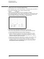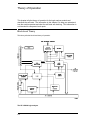
1
Errata Title & Document Type: 16524A State/Timing Logic Analyzer Service Guide Manual Part Number: 16542-90903 Revision Date: August 1992 HP References in this Manual This manual may contain references to HP or Hewlett-Packard. Please note that HewlettPackard's former test and measurement, semiconductor products and chemical analysis businesses are now part of Agilent Technologies. We have made no changes to this manual copy. The HP XXXX referred to in this document is now the Agilent XXXX. For example, model number HP8648A is now model number Agilent 8648A. About this Manual We’ve added this manual to the Agilent website in an effort to help you support your product. This manual provides the best information we could find. It may be incomplete or contain dated information, and the scan quality may not be ideal. If we find a better copy in the future, we will add it to the Agilent website. Support for Your Product Agilent no longer sells or supports this product. You will find any other available product information on the Agilent Test & Measurement website: www.tm.agilent.com Search for the model number of this product, and the resulting product page will guide you to any available information. Our service centers may be able to perform calibration if no repair parts are needed, but no other support from Agilent is available. Service Guide Publication number 16542-90903 First edition, August 1992 For Safety information, Warranties, and Regulatory information, see the pages at the end of the book. Copyright Hewlett-Packard Company 1992 All Rights Reserved. HP 16542A 2-Mbyte, 100-MHz State/Timing Logic Analyzer HP 16542A 2-Mbyte, 100-MHz State/Timing Logic Analyzer The HP 16542A is a 2-Mbyte, 100-MHz State/Timing Logic Analyzer module for the HP 16500A Logic Analysis System. The HP 16542A master offers the minimum configuration of 16 data channels, 1 clock input, and 1 clock/clock qualifier. Up to five HP 16542As can be connected to provide 80 channels of 1M deep data acquisition or 8 channels of 10M deep data acquisition using the E2430A Memory Expansion Interface. Features Some of the main features of the HP 16542A are as follows: • Time interval; number of states; pattern search; minimum, maximum, and average time interval statistics • Small, lightweight probing • Expandable to 80 data channels (one configured as a master and four configured as expanders) Service Strategy The service strategy for this instrument is the replacement of defective assemblies. This service guide contains information for finding a defective assembly by testing and servicing the HP 16542A analyzer module. This module can be returned to Hewlett-Packard for all service work, including troubleshooting. Contact your nearest Hewlett-Packard Sales Office for more details. ii The HP 16542A 2-Mbyte, 100-MHz State/Timing Logic Analyzer iii In This Book This book is the service guide for the HP 16542A 2-Mbyte, 100-MHz State/Timing Logic Analyzer module. Place this service guide in the 3-ring binder supplied with your HP 16500A Logic Analysis System Service Manual. This service guide is divided into eight chapters. Chapter 1 contains information about the module and includes accessories for the module, specifications and characteristics of the module, and a list of the equipment required for servicing the module. Chapter 2 tells how to prepare the module for use. Chapter 3 gives instructions on how to test the performance of the module. Chapter 4 contains calibration instructions for the module. Chapter 5 contains self-tests and flowcharts for troubleshooting the module. Chapter 6 tells how to replace the module and assemblies of the module and how to return them to Hewlett-Packard. Chapter 7 lists replaceable parts, shows an exploded view, and gives ordering information. Chapter 8 explains how the analyzer works and what the self-tests are checking. iv Contents 1 General Information Accessories 1–2 Specifications 1–3 Characteristics 1–4 Supplemental Characteristics 1–5 Recommended Test Equipment 1–8 2 Preparing for Use To inspect the module 2–2 To prepare the mainframe 2–3 To configure a one-card module 2–4 To configure a multicard module 2–5 To install the module 2–7 To turn on the system 2–8 To test the module 2–8 3 Testing Performance To test the performance 3–3 Testing a single-card module 3–3 Testing a multicard module 3–3 To test the stimulus port 3–4 Set up the equipment 3–4 Connect the logic analyzer 3–5 Set up the logic analyzer 3–6 Test the 4 ns/0 ns signal timing 3–7 Test the 2 ns/2 ns signal timing 3–8 Test the 0 ns/4 ns signal timing 3–9 Test the oscillator frequency 3–10 Exit the test 3–10 To perform the self-tests 3–11 Access the self-tests 3–11 Perform the Functional Tests 3–12 Perform the Calibration Dependent Tests 3–13 Test the expansion cards 3–15 Exit the self-tests 3–15 Performance Test Record 3–16 v Contents 4 Calibrating and Adjusting To calibrate the logic analyzer 4–3 Set up the logic analyzer 4–4 Calibrate the master clocking 4–5 Calibrate the expansion clocking 4–7 Save the calibration factors 4–8 Exit the calibration 4–9 To adjust the stimulus circuit 4–10 Install the extender board 4–11 Connect the logic analyzer 4–12 Locate the adjustments 4–13 Set up the oscilloscope 4–14 Set up the logic analyzer 4–14 Adjust the pulse width 4–15 Adjust the 4 ns/0 ns test port signal timing 4–16 Adjust the 2 ns/2 ns test port signal timing 4–17 Adjust the 0 ns/4 ns test port signal timing 4–18 Exit the adjustment 4–19 5 Troubleshooting To troubleshoot the analyzer 5–2 Follow the flowcharts 5–3 Test the auxiliary power 5–5 To run the self-tests 5–6 Access the self-tests 5–6 Perform the Functional Tests 5–7 Perform the Calibration Dependent Tests 6 Replacing Assemblies To remove the module 6–2 To replace the module 6–3 To replace the circuit board 6–4 To replace the probe cable 6–5 To return assemblies 6–6 7 Replaceable Parts Replaceable Parts Ordering 7–2 Replaceable Parts List 7–3 Exploded View 7–5 8 Theory of Operation Block-Level Theory 8–2 Self-Tests Description 8–5 vi 5–8 1 Accessories 1–2 Specifications 1–3 Characteristics 1–4 Supplemental Characteristics 1–5 Recommended Test Equipment 1–8 General Information General Information This chapter lists the accessories, the specifications and characteristics, and the recommended test equipment. Accessories The following accessories are supplied with the HP 16542A logic analyzer. Accessories Supplied Probe assemblies Grabbers, 20 per set Clock/ground lead Termination adapter Cable and pod labels Probe leads, 5 per set Probe grounds, 5 per set Cable and pod labels Probe cable ID clip Intercard cable connector kit Double probe adapter Composite operating software HP Part Number 01650-61608 5090-4356 16540-82101 01650-63203 16500-94303 5959-9333 5959-9334 16540-94306 16500-41201 16542-68701 16542-61607 Qty 1 2 1 1 1 1 1 1 1 1 1 Accessories Available • E2430A Memory Expansion Interface Other accessories available for the HP 16542A are listed in the Accessories for HP Logic Analyzers brochure. 1–2 General Information Specifications Specifications The specifications are the performance standards against which the product is tested. Maximum External Input Clock Rate: 100 MHz Setup/Hold Time:* Adjustable Setup 4 ns 2 ns 0 ns * Specified for an input signal : Hold 0 ns 2 ns 4 ns VH = −0.9 V, VL = −1.7 V, slew rate = 1 V/ns, threshold = −1.3 V. 1–3 General Information Characteristics Characteristics The characteristics are not specifications, but are included as additional information. Channel Count Maximum Sequencer Speed Internal Clock Rate Memory Depth Per Channel Trigger Width 16 channels 100 MHz 10 ns 1 048 576 (2 097 152 in half-channel mode) Pattern recognition to full width of analyzer at 100 MHz Input R 100 kΩ ±2% Input C Lead Sets Included ≈8 pf Yes (minigrabbers support through-hole and surface mount) 1–4 General Information Supplemental Characteristics Supplemental Characteristics Probes Input Resistance Input Capacitance 100 kΩ ± 2% ~ 8 pF Input Threshold Accuracy ±100 mV ±2% of threshold setting Input Dynamic Range Minimum Input Overdrive ±10V about the threshold 250 mV or 30% of the input amplitude, whichever is greater Maximum Input Voltage Minimum Voltage Swing ±40 V peak 500 mV, peak-to-peak Threshold Range −3.5 V to +5.0 V adjustable in 0.1-V increments State Analysis (External Clocking Mode) Clocks 2 Minimum Clock Pulse Width 3 ns Clock Qualifiers 1 Master-Slave Clocking (Mixed Clocking) Master must follow slave clock by at least 2 ns and precede the next slave clock by at least 11 ns. Timing Analysis (Internal Clocking Mode) Sample Period 10 ns Sec/Div 10 ns to 1000 s in a 1-2-5 sequence Triggering Pattern Recognizers Each recognizer is the AND combination of bit patterns (0, 1, or don’t care) in each label. Four pattern recognizers are available. Storage Qualification There are three storage qualifiers. No storage qualification is available in the internal clocking mode. Qualifier A user-specified term definable as anystate, nostate, a single pattern recognizer. 1–5 General Information Supplemental Characteristics Measurement and Display Functions Arming Each module can be armed by the RUN key, by the external PORT IN, or by another module via the Intermodule Bus (IMB). Displayed Waveforms 24 lines maximum, with scrolling across 96 waveforms. Measurement Functions Run/Stop Functions Run starts acquisition of data in specified trace mode. Stop In single trace mode or the first run of a repetitive acquisition, Stop halts acquisition and displays the current acquisition data. For subsequent runs in repetitive mode, Stop halts acquisition of data after one more complete measurement is made. Trace Mode Single mode acquires data once per trace specification. Repetitive mode repeats single mode acquisitions until Stop is pressed or until the user-defined stop condition has been satisfied. Indicators Activity Indicators Provided in the Configuration and Format menus for identifying high, low, or changing states on the inputs. Markers Two markers (X and O) are shown as dashed lines on the display. Trigger Displayed as a vertical dashed line in the Timing Waveform display and as line 0 in the State Listing display. Data Entry/Display Labels Channels may be grouped together and given a 6-character name. Up to 126 labels in each analyzer may be assigned with up to 32 channels per label. Display Modes State Listing, State Waveforms, Chart, Compare Listing, Compare Difference Listing, Timing Waveforms, and Timing Listings. Timing Waveforms and Oscilloscope Waveforms can be viewed on the same display. Timing Waveform Pattern readout of timing waveforms at X or O marker. Bases Binary, Octal, Decimal, Hexadecimal, ASCII (display only), Two’s Complement, and User-defined symbols. Symbols 500 maximum. Symbols can be downloaded over RS-232 or HP-IB. 1–6 General Information Supplemental Characteristics Marker Functions Time Interval The X and O markers measure the time interval between one point on a timing waveform and trigger, two points on the same timing waveform, or two points on different waveforms. Patterns The X and O markers can be used to locate the nth occurrence of a specified pattern from trigger, or from the beginning of data. The O marker can also find the nth occurrence of a pattern from the X marker. Statistics X and O marker statistics are calculated for repetitive acquisitions. Patterns must be specified for both markers, and statistics are kept only when both patterns can be found in an acquisition. Statistics are minimum X to O time, maximum X to O time, average X to O time, number of valid runs, and number of total runs. Auxiliary Power Power Through Cables 1/3 amp at 5 V maximum per cable Operating Environment Temperature Humidity Altitude Vibration Instrument, 0 °C to 55 °C (+32 °F to 131 °F). Probe lead sets and cables, 0 °C to 65 °C (+32 °F to 149 °F). Instrument, probe lead sets, and cables, up to 95% relative humidity at +40 °C (+122 °F). To 4600 m (15,000 ft). Operating: Random vibration 5 to 500 Hz, 10 minutes per axis, ≈0.3 g (rms). Non-operating: Random vibration 5 to 500 Hz, 10 minutes per axis, ≈ 2.41 g (rms); and swept sine resonant search, 5 to 500 Hz, 0.75 g (0-peak), 5 minute resonant dwell at 4 resonances per axis. 1–7 General Information Recommended Test Equipment Recommended Test Equipment Equipment Required Equipment Critical Specifications Recommended Model/Part Use* Digitizing Oscilloscope ≥ 6 GHz bandwidth, < 58 ps rise time HP 54121T P,A SMA (m)(m) Cable, Qty 3 > 3 GHz Bandwidth HP 8120-4977 P,A Termination Adapter No Substitute HP 01650-63203 P,A Extender Board No Substitute HP 16500-69004 A Test Adapter No Substitute HP 16540-66549 P,A,T Alignment Tool None HP 8710-1355 A * A = Adjustment 1–8 P = Performance Tests T = Troubleshooting 2 To inspect the module 2–2 To prepare the mainframe 2–3 To configure a one-card module 2–4 To configure a multicard module 2–5 To install the module 2–6 To turn on the system 2–8 To test the module 2–8 Preparing for Use Preparing For Use This chapter gives you instructions for preparing the logic analyzer module for use. Power Requirements All power supplies required for operating the logic analyzer are supplied through the backplane connector in the mainframe. Operating Environment The operating environment is listed in chapter 1. Note the noncondensing humidity limitation. Condensation within the instrument can cause poor operation or malfunction. Provide protection against internal condensation. The logic analyzer module will operate at all specifications within the temperature and humidity range given in chapter 1. However, reliability is enhanced when operating the module within the following ranges: • Temperature: +20 °C to +35 °C (+68 °F to +95 °F) • Humidity: 20% to 80% noncondensing Storage Store or ship the logic analyzer in environments within the following limits: • Temperature: −40 °C to + 75 °C • Humidity: Up to 90% at 65 °C • Altitude: Up to 15,300 meters (50,000 feet) Protect the module from temperature extremes which cause condensation on the instrument. To inspect the module 1 Inspect the shipping container for damage. If the shipping container or cushioning material is damaged, keep them until you have checked the contents of the shipment and checked the instrument mechanically and electrically. 2 Check the supplied accessories. Accessories supplied with the module are listed in "Accessories" in chapter 1. 3 Inspect the product for physical damage. Check the module and the supplied accessories for obvious physical or mechanical defects. If you find any defects, contact your nearest Hewlett-Packard Sales Office. Arrangements for repair or replacement are made, at Hewlett-Packard’s option, without waiting for a claim settlement. 2–2 Preparing for Use To prepare the mainframe To prepare the mainframe CAUTION CAUTION Turn off the mainframe power before removing, replacing, or installing the module. Electrostatic discharge can damage electronic components. Use grounded wriststraps and mats when performing any service to this module. 1 Turn off the mainframe power switch, then unplug the power cord. Disconnect any input or output connections. 2 Plan your module configuration. If you are installing a one-card module, use any available slot in the mainframe. If you are installing a multicard module, use adjacent slots in the mainframe. 3 Loosen the thumb screws. Cards or filler panels below the slots intended for installation do not have to be removed. Starting from the top, loosen the thumb screws on filler panels and cards that need to be moved. 2–3 Preparing for Use To configure a one-card module 4 Starting from the top, pull the cards and filler panels that need to be moved halfway out. CAUTION All multicard modules will be cabled together. Pull these cards out together to prevent damage to the cables and connectors. 5 Remove the cards and filler panels. Remove the cards or filler panels that are in the slots intended for the module installation. Push all other cards into the card cage, but not completely in. This is to get them out of the way for installing the module. Some modules for the Logic Analysis System require calibration if you move them to a different slot. For calibration information, refer to the manuals for the individual modules. To configure a one-card module • When shipped separately, the module is configured as a one-card module. • If you need to configure a multicard module into a one-card module, remove the cables connecting the cards. 2–4 Preparing for Use To configure a multicard module To configure a multicard module To configure a multicard module, connect the cable as follows. Save unused cables for future configurations. • To configure a two-card module, connect the cable from the master-configured card to the expansion card. The master card goes in the bottom position of the module. • To configure a 3-card module, connect the cable from the master-configured card to the expansion cards. The master card goes in the middle position of the module. 2–5 Preparing for Use To configure a multicard module • To configure a 4-card module, connect the cable from the master-configured card to the expansion cards. The master card goes in the slot next to the bottom position of the module. • To configure a 5-card module, connect the cable from the master-configured to the expansion cards. The master card goes in the middle position of the module. 2–6 Preparing for Use To install the module To install the module 1 Slide the cards above the slots for the module about halfway out of the mainframe. 2 If the module consists of a single card, then slide the module approximately halfway into the mainframe. If the module consists of more than one card, then perform the following steps: a Slide the card approximately halfway into the mainframe. b Feed the intercard cable up through the slot in the card, then connect the cable to the card. Repeat steps a and b for the remaining cards of the module. 3 Slide the complete module into the mainframe, but not completely in. Each card in the instrument is firmly seated and tightened one at a time in step 5. 4 Position all cards and filler panels so that the endplates overlap. 5 Seat the cards and tighten the thumbscrews. Starting with the bottom card, firmly seat the cards into the backplane connector of the mainframe. Keep applying pressure to the center of the card endplate while tightening the thumbscrews finger-tight. Repeat this for all cards and filler panels starting at the bottom and moving to the top. WARNING For correct air circulation, filler panels must be installed in all unused card slots. Correct air circulation keeps the instrument from overheating. Keep any extra filler panels for future use. 2–7 Preparing for Use To turn on the system To turn on the system 1 Connect the power cable to the mainframe. 2 Insert the disk containing the operating system into the front or rear disk drive. 3 Turn on the power switch. When you turn on the power switch, the logic analyzer performs power-up tests that check mainframe circuitry. After the power-up tests are complete, the screen will look similar to the sample screen below. To test the module • If you require a test to verify the specifications, start at the beginning of chapter 3, "Testing Performance." • If you require a test to initially accept the operation, perform the self-tests in chapter 3. • If you need to calibrate or adjust the module, go to chapter 4, "Calibrating and Adjusting." • If the module does not operate correctly, go to the beginning of chapter 5, "Troubleshooting." 2–8 3 To test the performance 3–3 To perform the stimulus port test 3–4 To perform the self-tests 3–11 Performance Test Record 3–16 Testing Performance Testing Performance This chapter tells you how to test the performance of the logic analyzer against the specifications listed in chapter 1. To ensure the logic analyzer is operating as specified, software tests (self-tests) and manual performance tests are done on the module. The logic analyzer is considered performance-verified if all of the software tests and manual performance tests have passed. The procedures in this chapter indicate what constitutes a "Pass" status for each of the tests. Test Strategy The performance verification tests consist of verifying the operation of the stimulus ports and of performing the self-tests. Perform the tests at the environmental operating temperature of the instrument. If a card fails the stimulus port test, go to chapter 5, "Troubleshooting." Test Interval Test the performance of the module at two-year intervals, or if it is replaced or repaired. Performance Test Record A performance test record for recording the results of each procedure is located at the end of this chapter. Use the performance test record to gauge the performance of the module over time. Test Equipment Each procedure lists the recommended test equipment. You can use equipment that satisfies the specifications given. However, the procedures are based on using the recommended model or part number. Instrument Warm-Up Before testing the performance of the module, warm-up the instrument and the test equipment for 30 minutes. Initial Acceptance If you require a test to initially accept the operation of the logic analyzer, perform the self-tests. See Also "To perform the self-tests," on page 3–11. 3–2 To test the performance All tests are performed on single-card modules. Multicard modules must be reconfigured as single-card modules before testing the performance. Testing a single-card module 1 Turn on the mainframe and allow it to warm up for 30 minutes. 2 Test the stimulus port. Refer to "To test the stimulus port" on page 3–4 for the test procedure. 3 If the single-card module failed the stimulus port test, adjust the stimulus circuit. Refer to chapter 4, "Calibrating and Adjusting" for the adjustment procedure. 4 Perform the self-tests. If a card failed the self-tests, replace the card, then retest it. When the self-test are complete, store the calibration factors to disk if desired. Refer to "To perform the self-tests" on page 3–11 for the test procedure. Testing a multicard module 1 Turn off the mainframe, remove the multicard module, then reconfigure the multicard module into single-card modules. Refer to chapter 6, "Removing Assemblies" for removal instructions. Refer to chapter 2, "Preparing For Use" for configuration and installation instructions. 2 Turn on the mainframe and allow it to warm up for 30 minutes. 3 Test the stimulus port on each of the cards. If a card fails, note the failed card, then test the next card. Refer to "To test the stimulus ports" on page 3–4 for the test procedure. 4 If any card failed the stimulus port test, adjust the stimulus port on the failed card. Refer to chapter 4, "Calibrating and Adjusting" for the adjustment procedure. 5 Perform the self-tests on each of the cards . If a card fails, note the failed card, then test the next card. Do not store any calibration factors to disk. Refer to "To perform the self-tests" on page 3–11 for the test procedure. 6 If any card failed the self-tests, replace the card, then test the new card. 7 When all single-card modules are tested, turn off the mainframe, then remove the single-card modules. Reconfigure the modules into a multicard module, then reinstall the multicard module into the mainframe. Refer to chapter 2, "Preparing For Use" for configuration and installation instructions. 8 Turn on the mainframe, then perform the self-tests on the multicard module. When the self-tests are complete, store the calibration factors to disk if desired. 3–3 To test the stimulus port Testing the stimulus port verifies that the stimulus on the HP 16542A logic analyzer operates properly. Multicard modules must be reconfigured as one-card modules for this test. During this test, output waveforms of the stimulus ports are characterized at different setup/hold configurations. The stimulus ports are used by the self-tests and by the calibration procedure. If the waveforms of the stimulus circuit are not correct, perform the adjustment procedure in chapter 4, "To adjust the stimulus circuit." Equipment Required Equipment Critical Specifications Recommended Model/Part Qty Digitizing Oscilloscope ≥ 6 GHz bandwidth , <58 ps rise time HP 54121T 1 Test Adapter HP 16540-66549 2 SMA Cable HP 8120-4977 3 Set up the equipment 1 Turn on the equipment required. Insert the operating system into a disk drive, then turn on the logic analyzer. Let them warm up for 30 minutes before beginning the test. 2 Set up the oscilloscope. On a calibrated HP 54121T oscilloscope, set the probe attenuation to 10.28:1 for Channel 1, Channel 2, and Trigger. Configure the oscilloscope according to the following information: Oscilloscope Setup Channel 1 Channel 2 Time Base Trigger Display 195.3 mV/Div 195.3 mV/Div 1 ns/Div HF Reject: Off Display Mode: Persistence Offset −1.3 V Offset −1.3 V Trig Level: −1.302 V Screen: Single V_markers: −1.3001 V V_markers: −1.3001 V Slope: Pos 3–4 Testing Performance To test the stimulus port Connect the logic analyzer 1 Remove the connector plugs from the stimulus ports located on the HP 16542A master-configured card. 2 Connect one test adapter to stimulus port 1 of the HP 16542A. Connect one SMA cable from channel 1 of the oscilloscope to the DATA output of the test adapter in stimulus port 1. Connect one SMA cable from channel 2 of the oscilloscope to the CLK output of the test adapter in stimulus port 1. The test adapter is shown below. 3 Connect one test adapter to stimulus port 2 of the HP 16542A. Connect one SMA cable from Trig of the oscilloscope to the CLK output of the test adapter in stimulus port 2. Test Adapter Equipment Setup 3–5 Testing Performance To test the stimulus port Set up the logic analyzer 1 In the System Configuration menu, touch System. Then, touch 2 MB Data Acq in the pop-up menu. 2 In the 2 MB Data Acq Configuration menu, touch Configuration. Then, touch Calibration in the pop-up menu. 3 In the Calibration menu, touch Cal Mode Select. In the pop-up menu, touch 4/0 ns. 4 Touch Pattern Generator Off to change the field to Pattern Generator On. When the pattern generator turns on, the oscilloscope will trigger. 3–6 Testing Performance To test the stimulus port Test the 4 ns/0 ns signal timing Verify the 4 ns/0 ns test port signal timing relationship. 1 In the oscilloscope Timebase menu, use the Delay to center the falling edges of the waveforms on the oscilloscope screen. 2 In the oscilloscope Display menu, make the following changes: Display Mode Averaged Number of Averages 32 3 In the oscilloscope Delta-V and Delta-T menus, make the following changes: Delta-V menu Marker 1 Position Chan 2 Marker 1 at −1.3001 V Marker 2 Position Chan 1 Marker 2 at −1.3001 V Delta-T menu Start On NEG Edge 1 Stop On NEG Edge 1 The Start field will be green to correspond with channel 2. 4 In the oscilloscope Delta-T menu, select Precise Edge Find. Verify that the cursors fall on legitimate falling edges and not on false edges. In the data field at the bottom of the display, the Delta-T will display a value between −150.0 ps and −40 ps. 5 In the oscilloscope Delta-T menu, make the following change: Stop On POS Edge 1 6 In the oscilloscope Delta-T menu, select Precise Edge Find. Verify that the cursors fall on legitimate edges and not on false edges. In the data field at the bottom of the display, the Delta-T will display a value between −3.620 ns to −3.900 ns. 7 In the oscilloscope Delta-T menu, make the following change: Stop On NEG Edge 1 3–7 Testing Performance To test the stimulus port Test the 2 ns/2 ns signal timing Verify the 2 ns/2 ns test port signal timing relationship. 1 In the Calibration menu, touch Cal Mode Select. In the pop-up menu, touch 2/2 ns. 2 Clear the oscilloscope display, then wait for averaging to complete. 3 In the oscilloscope Delta-T menu, select Precise Edge Find. Verify that the cursors fall on legitimate falling edges and not false edges. In the data field at the bottom of the display, the Delta-T will display a value between 1.780 ns and 1.970 ns. 4 In the oscilloscope Delta-T menu, make the following change: Stop On POS Edge 1 5 In the oscilloscope Delta-T menu, select Precise Edge Find. Verify that the cursors fall on legitimate edges and not false edges. In the data field at the bottom of the display, the Delta-T will display a value between −1.610 ns and −1.970 ns. 6 In the oscilloscope Delta-T menu, make the following change: Stop On NEG Edge 1 3–8 Testing Performance To test the stimulus port Test the 0 ns/4 ns signal timing Verify the 0 ns/4 ns test port signal timing relationship. 1 In the Calibration menu, touch Cal Mode Select. In the pop-up menu, touch 0/4 ns. 2 Clear the oscilloscope display, then wait for averaging to complete. 3 In the oscilloscope Delta-T menu, select Precise Edge Find. Verify that the cursors fall on legitimate falling edges and not false edges. In the data field at the bottom of the display, the Delta-T will display a value between 3.620 ns and 3.900 ns. 4 In the oscilloscope Delta-T menu, make the following change: Stop On POS Edge 1 5 In the oscilloscope Delta-T menu, select Precise Edge Find. Verify that the cursors fall on legitimate edges and not false edges. In the data field at the bottom of the display, the Delta-T will display a value between 0.040 ns and 0.150 ns. 6 In the oscilloscope Delta-T menu, make the following change: Stop On NEG Edge 1 3–9 Testing Performance To test the stimulus port Test the oscillator frequency Verify the oscillator frequency. 1 In the Calibration menu, touch Cal Mode Select. In the pop-up menu, touch 2/2 ns. 2 On the oscilloscope, make the following changes: Time base menu Time/div 4 ns/div Delta-V menu Marker 1 Position Channel 2 Marker 2 Position Channel 2 Marker 1 at −1.3001 V Marker 2 at −1.3001 V Delta-T menu Start On NEG Edge 2 Stop On NEG Edge 3 The Start On and Stop On fields will be green to correspond with channel 2. 3 In the oscilloscope Delta-T menu, select Precise Edge Find. Verify that the cursors fall on legitimate falling edges and not on false edges. In the data field at the bottom of the display, the Delta-T will display 10.00 ns ±0.11 ns. Exit the test 1 In the Configuration menu, touch Cal Mode Select. In the pop-up menu, touch Off. 2 Disconnect the test adapters and the SMA cables from the oscilloscope and from the HP 16542A. 3 Install the connector plugs on the stimulus ports. 3–10 To perform the self-tests The self-tests verify the correct operation of the logic analyzer module and verify the module specifications. Using signals from the stimulus ports, portions of the self-tests and calibration verify the specifications listed in chapter 1. The self-tests consist of Functional Tests and Calibration Dependent Tests. During the self-tests, a calibration is performed. If the calibration passes, then those calibration factors can be stored and used to operate the module. If a self-test fails, refer to chapter 5, "Troubleshooting." Self-tests can be performed all at once or one at a time. While testing the performance of the module, run the self-tests all at once. Access the self-tests 1 Disconnect all inputs, insert the disk containing the operating system into a disk drive, then turn on the power switch. 2 In the System Configuration menu, touch Configuration. In the pop-up, touch Test. 3 Remove the disk containing the operating system, then insert the disk containing the performance verification (self-tests) into the disk drive. Touch the box labeled Touch box to Load Test System. 4 On the test system screen, touch Test System. Select the 2 MB Data Acq module to be tested. The screen displays the main test menu. 3–11 Testing Performance To perform the self-tests Perform the Functional Tests 1 Touch Functional Tests. The screen displays the Functional Tests menu. The status of each test—UNTESTED, PASSED, or FAILED—is displayed below the test name. When performing the Functional Tests, you can run all tests automatically or run each test individually. If the Functional Tests are run individually, screens containing test information are provided. This performance verification procedure gives instructions to run all tests automatically. 2 Touch All Tests to run all Functional Tests automatically. Each test runs one time, and the screen lists the name of the test as the test runs. The Functional Tests take approximately 3 minutes per module. When the Functional Tests are all complete, the status of each test updates to passed or failed. 3 Touch Exit on the Functional Tests menu. The screen displays the main self-test menu. 3–12 Testing Performance To perform the self-tests Perform the Calibration Dependent Tests 1 Remove the connector plugs from the HP 16542A master-configured card. 2 In the main self-test menu, touch Calibration and Associated Tests. 3 Obtain calibration factors by touching one of the boxes on the screen. The Calibration Dependent Tests need calibration factors loaded into the memory before the tests can be run. The calibration factors are obtained by performing the calibration or by loading previously stored calibration factors. a To load calibration factors from a disk, touch Load Calibration Factors From Disk. Because the system accesses the rear disk drive first, a calibration file located in the rear disk drive will be loaded. If the rear disk drive does not have a calibration file, then a calibration file located in the front disk drive will be loaded. b To perform the calibration, touch Perform Master Clocking Calibration, then follow the instructions on the screen. The calibration procedure screens give instructions to connect the logic analyzer pods to the stimulus ports on the rear panel of the logic analyzer master-configured card. At the conclusion of the calibration, choices are available to save the calibration factors or not to save them. This calibration is the same as the calibration procedure accessed in the Configuration menu, except that this calibration procedure is performed during the self-tests. For help with the step-by-step calibration procedure, see chapter 4, "Calibrating and Adjusting." 3–13 Testing Performance To perform the self-tests 4 Following the instructions on the screen, connect the pod of the master-configured card to test stimulus port 2 on the card using a termination adapter. In this example, the master-configured card is represented by B1. When performing the Calibration Dependent Tests, you can run all the tests on the pod or run each test individually. This performance verification procedure gives instructions to run all the tests on the pod. 5 In the Calibration Dependent Tests menu, touch All Tests. All the Calibration Dependent Tests automatically test the pod of the master-configured card. 6 If the module consists of only one card, go to "Exit the self-tests" on the next page. If the module includes expansion-configured cards, go to "Test the expansion cards" on the next page. 3–14 Testing Performance To perform the self-tests Test the expansion cards 1 In the Calibration Dependent Tests menu, touch the box in the lower, left of the screen to select another pod. For this example, B1 (the pod of the master-configured card) in the lower-left of the screen was touched. Then the screen displayed the pop-up menu listing the other pods. 2 In the pop-up menu, touch the box representing the next pod to test. In this example, touch A1 (the pod of an expansion-configured card). The screen gives instructions for the test. 3 Following the instructions on the screen, move the pod of the master-configured card to test stimulus port 1, connect the pod of the first expansion-configured card to stimulus port 2, then touch All Tests. All of the Calibration Dependent Tests automatically test the pod of the expansion card. 4 Continue selecting the pods and following the instructions on the screen to connect and disconnect the pods until all the pods of the expansion cards are tested. 5 To exit the Calibration Dependent Tests, touch Exit on the Calibration Dependent Tests menu. The screen displays the main self-test menu and reports the status of the Calibration Dependent Tests. 6 Install the connector plugs in the stimulus ports located on the master-configured card. Exit the self-tests 1 To exit the main self-test menu, touch the fields in the following sequence: 2 MB Data Acq Test System Configuration Exit Test 2 Insert the operating system disk into a disk drive. Then, touch the box located near the top-center of the screen to exit the test system. The screen displays the System Configuration menu. 3–15 Performance Test Record Performance Test Record HP 16542A 2-Mbyte, 100-MHz State/Timing Logic Analyzer_______ Serial No.______________________ Work Order No.___________________ Recommended Test Interval - 2 Year/4000 hours Date___________________ Recommended next testing___________________ Temperature___________________ Test Stimulus Port Test Settings Results ________ ________ ________ ________ ________ 4/0 ns 2/2 ns 0/4 ns Oscillator frequency Self-Tests Pass/Fail 3–16 _________ 4 To calibrate the logic analyzer 4–3 To adjust the stimulus circuit 4–10 Calibrating and Adjusting Calibrating and Adjusting This chapter gives you instructions for calibrating and adjusting the logic analyzer. Calibration Strategy The HP 16542A calibration optimizes the relationship between the master and expansion clocks and the incoming data for the three setup and hold configurations, accommodating any channel-to-channel skew generated by the probe cables and by the logic analyzer. Before a calibration is performed, the setup and hold selections are not available in the state clocking Format menu. Calibration Interval To maintain proper operation of the HP 16542A analyzer, periodic calibration is recommended. If the module is used under normal operating conditions, perform the calibration at approximately six-month or 1,000-hour intervals. Perform a calibration if the environment changes more than 10 °C, if the module is inserted in a different card slot, or if the module is reconfigured. Adjustment Strategy The adjustment procedure consists of installing the analyzer on an extender board, then adjusting the timing relationships and the pulse width of the stimulus circuit. Adjustment Interval New modules are adjusted at Hewlett-Packard to meet specifications. Before any adjustments are made to the module, complete the performance tests in chapter 3,"Testing Performance." If the performance tests are within specifications, then adjustments are not necessary. Test Equipment Each procedure lists the recommended test equipment. You can use equipment that satisfies the specifications given. However, the procedures are based on using the recommended model or part number. Instrument Warm-up Perform the adjustments at the environmental ambient temperature of the instrument, and after a 30-minute warmup of the module and the test equipment. 4–2 To calibrate the logic analyzer The calibration is performed on the pod of the master-configured card first, then on the pods of each attached expansion-configured card. If the module includes expansion-configured cards, expansion clocking calibration can be performed after master clocking calibration is complete. This procedure gives instructions to calibrate the logic analyzer module and to store the calibration factors to a disk. Using termination adapters to connect pod cables to test stimulus ports, follow the prompts on the screen to connect and disconnect the pod cables. The calibration performed in this procedure operates the same as the calibration performed during the self-tests. To verify the operation of the module and to perform a calibration at the same time, you can perform the self-tests. Refer to "To perform the self-tests" in chapter 3. Performing the self-tests requires using the Performance Verification disk. If you would like to verify the calibration waveforms of the stimulus port before performing a calibration, follow the stimulus test procedure in chapter 3, "Testing Performance." For multicard modules, perform the stimulus port test on the master-configured card only, because the stimulus port on an expander-configured card is inoperative. Equipment Required Equipment Termination Adapter Critical Specification Recommended Model/Part Qty HP 01650-63203 2 4–3 Calibrating and Adjusting To calibrate the logic analyzer Set up the logic analyzer 1 Insert the operating system disk into a disk drive, then turn on the instrument. Remove the connector plugs located in the stimulus ports on the master-configured card. 2 In the System Configuration menu, touch System, then touch 2 MB Data Acq in the pop-up menu. Touch Configuration, then touch Calibration in the pop-up menu. 4–4 Calibrating and Adjusting To calibrate the logic analyzer Calibrate the master clocking 1 Touch Perform Master Clocking System Calibration in the Calibration menu. 2 Follow the instructions on the screen to connect the pod from the master-configured card through a termination adapter to test stimulus port 1. The test stimulus ports are labeled on the rear panel of the HP 16542A master-configured card. Touch Proceed. An asterisk will flash in the upper, right corner of the screen while calibration is in progress. 3 If the module consists of a single card, the calibration procedure is complete when the pod is calibrated. Go to "Save the calibration factors" on page 4–8 to store the calibration values. If the module consists of a master-configured card and one or more expansion-configured cards, continue with step 4. 4–5 Calibrating and Adjusting To calibrate the logic analyzer 4 Move the master card pod to test stimulus port 2, connect the pod of the first expansion-configured card to be calibrated to test stimulus port 1. Then, touch Proceed. 5 Continue following instructions on the screen to connect the various pods to the test stimulus ports, until all of the expansion-configured card pods are calibrated with the master clock. 4–6 Calibrating and Adjusting To calibrate the logic analyzer Calibrate the expansion clocking 1 The expander clocking system can be calibrated or skipped. • To perform the expansion clocking calibration, touch Perform Expander Clocking Calibration. • To skip the expansion clocking calibration, touch Skip Expander Clocking Calibration. For applications using only master clocking, master clocking calibration is sufficient and expansion clocking calibration need not be performed. To use expansion clocking in applications, perform the expansion clocking calibration. 2 Follow the step-by-step instructions on the screen to connect the pods of the expansion-configured cards to the test stimulus ports on the master-configured card. 4–7 Calibrating and Adjusting To calibrate the logic analyzer Save the calibration factors When the calibration is complete, the choice is given to save the calibration factors or to not save the calibration factors. 1 Choose to save or not save the calibration factors. • To not save the calibration factors, touch Do Not Save Cal Factors To Disk, then go to the next page. • To save the calibration factors, touch Save Cal Factors To Disk. 2 A keypad pop-up appears on the screen. Before storing the calibration factors to a disk, you can use the keypad pop-up to enter a description of the file to contain the calibration factors or use the default description provided. Important information to include in the description may be the calibration date and time, and the HP 16542A serial suffix. 3 Touch Done, and the calibration factors are stored to the disk. The calibration software accesses the rear disk drive first, then accesses the front disk drive. If a disk is in the rear disk drive, the file with calibration factors will be saved to the disk in the rear disk drive. 4–8 Calibrating and Adjusting To calibrate the logic analyzer Exit the calibration 1 To exit the calibration menu, touch Calibration. Then, touch Configuration in the pop-up menu. 2 Install the connector plugs in the stimulus ports on the logic analyzer card. 4–9 To adjust the stimulus circuit The stimulus circuit adjustment is the only hardware adjustment. This adjustment is preset at Hewlett-Packard and normally should not need adjustment. The characteristics of the stimulus circuit are tested in chapter 3, "Testing Performance." If those characteristics are not the correct value, perform the stimulus circuit adjustment. This procedure describes adjusting the timing relationships and the pulse width of the stimulus circuit. Adjustable delay lines on the HP 16542A are used to perform the adjustment. Perform the adjustments at the environmental ambient temperature of the instrument and after a 30-minute warmup of the module and the test equipment. Equipment Required Equipment Recommended Model/Part Qty Digitizing Oscilloscope HP 54121T 1 Test Adapter HP 16540-66549 2 SMA Cable HP 8120-4977 3 Alignment Tool HP 8710-1355 1 4–10 Critical Specification Calibrating and Adjusting To adjust the stimulus circuit Install the extender board • You can install the extender board in any empty slot of the card cage. • If other modules are installed in the card cage, it will be easier to use the same slot where the logic analyzer module under test was located. • Cards or filler panels below the slot intended for extender board installation do not have to be moved. CAUTION Electrostatic discharge can damage electronic components. Use grounded wriststraps and mats when performing any service to this module. 1 Turn off the instrument power switch, then unplug the power cord. Disconnect any input connections. 2 Starting from the top, loosen the thumb screws on the filler panels and cards. 3 Starting from the top, pull the cards and filler panels out halfway. 4 Pull out the card to be serviced. 5 Push all other cards back into the card cage, but not completely in, so they will be out of the way for the extender board installation. 6 Slide the extender board completely into the card cage, making sure it is firmly seated in the backplane connector. 7 Plug the logic analyzer card into the extender board. 4–11 Calibrating and Adjusting To adjust the stimulus circuit Connect the logic analyzer 1 Install the logic analyzer card on an extender board. For the installation of the extender board, refer to "Install the Extender Board" on the previous page. Remove the connector plugs from the stimulus ports located on the logic analyzer card. CAUTION To prevent damage to the components on the logic analyzer card, use a cooling fan on the bottom one-third portion of the card (closest to the extender board) when the card is on the extender board. 2 Connect one test adapter to stimulus port 1 of the logic analyzer. Connect one SMA cable from channel 1 of the oscilloscope to the DATA output of the test adapter in stimulus port 1. Connect one SMA cable from channel 2 of the oscilloscope to the CLK output of the test adapter in stimulus port 1. 3 Connect one test adapter to stimulus port 2 of the logic analyzer. Connect one SMA cable from Trig of the oscilloscope to the CLK output of the test adapter in stimulus port 2. Test Adapter Equipment Setup 4–12 Calibrating and Adjusting To adjust the stimulus circuit Locate the adjustments • The figure shows the location of the adjustable delay lines on the logic analyzer. Delay Line Location 4–13 Calibrating and Adjusting To adjust the stimulus circuit Set up the oscilloscope On a calibrated HP 54121T oscilloscope, set the probe attenuation to 10.28:1 for Channel 1, Channel 2, and Trigger. Configure the oscilloscope according to the following table. Oscilloscope Setup Channel 1 Channel 2 Time Base Trigger Delta-V Display 195.3 mV/Div 195.3 mV/Div 1 ns/Div HF Reject Off V Markers On Mode Persistence Offset −1.300 V Offset −1.300 V Trig Level −1.302 V Marker 1 Position Channel 1 Marker 1 at −1.3001 V Screen Single V_markers −1.3001 V V_markers −1.3001 V Slope Pos Marker 2 Position Channel 1 Marker 2 at −1.3001 V Set up the logic analyzer 1 Insert the operating system disk into a disk drive, then turn on the instrument. 2 In the System Configuration menu, touch System. Then, touch 2 MB Data Acq in the pop-up menu. 3 In the Calibration menu, touch Cal Mode Select. In the pop-up menu, touch 4/0 ns. 4 Touch Pattern Generator Off to change the field to Pattern Generator On. When the pattern generator turns on, the oscilloscope will trigger. 4–14 Calibrating and Adjusting To adjust the stimulus circuit Adjust the pulse width 1 In the oscilloscope Timebase menu, use the Delay to center the falling edges of the waveforms on the oscilloscope screen. 2 In the oscilloscope Display menu, make the following changes: Display Mode Averaged Number of Averages 32 3 Clear the oscilloscope display, then wait for averaging to complete. 4 In the oscilloscope Delta-T menu, make the following changes: T markers On Start On POS Edge 1 Stop On NEG Edge 1 The Start On and Stop On fields will be yellow to correspond with channel 1. 5 In the oscilloscope Delta-T menu, select Precise Edge Find. Verify that the cursors fall on legitimate edges and not on false edges. In the data field at the bottom of the display, the Delta-T will display a value between 3.650 ns and 3.750 ns. 6 If the correct pulse width is observed, go the next page. If the correct pulse width is not observed, perform the following steps: a In the oscilloscope Display menu, set the number of averages to 4. b Using the alignment tool, adjust the pulse width delay line a slight amount. Refer to page 4–13, "Locate the adjustments," for the location of the delay line. After the adjustment, select Precise Edge Find on the oscilloscope Delta-T menu. Verify that the markers fall on legitimate edges of the waveform. c Repeat the above step until the pulse width (Delta-T) is between 3.650 ns and 3.750 ns. d In the oscilloscope Display menu, set the number of averages 32. Wait for averaging to complete. In the oscilloscope Delta-T menu, select Precise Edge Find. In the data field at the bottom of the display, the Delta-T will display a value between 3.650 ns and 3.750 ns with the cursors on legitimate edges. 4–15 Calibrating and Adjusting To adjust the stimulus circuit Adjust the 4 ns/0 ns test port signal timing 1 In the oscilloscope Delta-V and Delta-T menus, make the following changes: Delta-V menu: Marker 1 Position Chan 2 Marker 2 Position Chan 1 Marker 1 at −1.3001 V Marker 2 at −1.3001 V Delta-T menu: Start On Stop On NEG edge 1 NEG Edge 1 The Start field will be green to correspond with channel 2. 2 In the oscilloscope Delta-T menu, select Precise Edge Find. Verify that the cursors fall on legitimate edges and not on false edges. In the data field at the bottom of the display, the Delta-T will show a value between −150.0 ps and −50 ps. 3 If the correct timing relationship is observed, go to the next page. If the correct timing relationship is not observed, perform the following steps: a In the oscilloscope Display menu, set the number of averages to 4. b Using the adjustment tool, adjust the 4 ns/0 ns delay line a slight amount. Refer to page 4–13, "Locate the adjustments," for the location of the delay line. After the adjustment, select Precise Edge Find on the oscilloscope Delta-T menu. Verify that the markers fall on legitimate edges of the waveform. c Repeat the above step until the falling edges (Delta-T) are between −150.0 ps to −50 ps apart. d In the oscilloscope Display menu, set the number of averages to 32. Wait for averaging to complete. In the oscilloscope Delta-T menu, select Precise Edge Find. In the data field at the bottom of the display, the Delta-T will display −150.0 ps to −50 ps with the cursors on legitimate edges. 4–16 Calibrating and Adjusting To adjust the stimulus circuit Adjust the 2 ns/2 ns test port signal timing 1 In the Calibration menu, touch Cal Mode Select. In the pop-up menu, touch 2/2 ns. 2 Clear the oscilloscope display, then wait for averaging to complete. 3 In the oscilloscope Delta-T menu, select Precise Edge Find. Verify that the cursors fall on legitimate edges and not false edges. In the data field at the bottom of the display, the Delta-T will display a value between 1.870 ns and 1.970 ns. 4 If the correct timing relationship is observed, go to the next page. If the correct timing relationship is not observed, perform the following steps: a In the oscilloscope Display menu, set the number of averages to 4. b Using the alignment tool, adjust the 2 ns/2 ns delay line a slight amount. Refer to page 4–13, "Locate the adjustments," for the location of the delay line. After the adjustment, select Precision Edge Find on the oscilloscope Delta-T menu. Verify that the markers fall on legitimate edges of the waveform. c Repeat the above step until the falling edges (Delta-T) are between 1.870 ns and 1.970 ns apart. d In the oscilloscope Display menu, set the number of averages to 32. Wait for averaging to complete. In the oscilloscope Delta-T menu select Precise Edge Find. In the data field at the bottom of the display, the Delta-T will display a value between 1.870 ns and 1.970 ns with the cursors on legitimate edges. 4–17 Calibrating and Adjusting To adjust the stimulus circuit Adjust the 0 ns/4 ns test port signal timing 1 In the Calibration menu, touch Cal Select Mode. In the pop-up menu, touch 0/4 ns. 2 In the oscilloscope Delta-T menu, make the following change: Stop On POS Edge 1 Clear the oscilloscope display, then wait for averaging to complete. 3 In the oscilloscope Delta-T menu, select Precise Edge Find. Verify that the cursors fall on legitimate edges and not false edges. In the data field at the bottom of the display, the Delta-T will display a value between 150 ps and 50 ps. 4 If the correct timing relationship is observed, go to the next page. If the correct timing relationship is not observed, perform the following steps: a In the oscilloscope Display menu, set the number of averages to 4. b Using the alignment tool, adjust the 0 ns/4 ns delay line a slight amount. Refer to page 4–13, "Locate the adjustments," for the location of the delay line. After the adjustment, select Precise Edge Find on the oscilloscope Delta-T menu. Verify the markers fall on legitimate edges of the waveform. c Repeat the above step until the edges (Delta-T) are between 150 ps and 50 ps apart. d In the oscilloscope Display menu, set the number of averages to 32. Wait for averaging to complete. In the oscilloscope Delta-T menu select Precise Edge Find. In the data field at the bottom of the display, the Delta-T will show between 150 ps and 50 ps with the cursors on legitimate edges. 4–18 Calibrating and Adjusting To adjust the stimulus circuit Exit the adjustment 1 Turn off the mainframe, then disconnect the test adapters and the SMA cables from the oscilloscope and from the logic analyzer. 2 Install the connector plugs in the stimulus ports located on the master-configured card. 3 Remove the logic analyzer from the extender board and reconfigure the mainframe. 4 Perform a calibration. Refer to "To calibrate the logic analyzer," on page 4–3 for the calibration procedure. 4–19 5 To troubleshoot the analyzer To run the self-tests 5–6 Troubleshooting 5–2 Troubleshooting This chapter helps you troubleshoot the module to find defective assemblies. The troubleshooting consists of flowcharts, self-test instructions, and a test for the auxiliary power supplied by the probe cable. This information is not intended for component-level repair. The service strategy for this instrument is the replacement of defective assemblies. This module can be returned to Hewlett-Packard for all service work, including troubleshooting. For replacement procedures, refer to chapter 6, "Replacing Assemblies." For the return procedure, refer to "To return assemblies" on page 6–6. Contact your nearest Hewlett-Packard Sales Office for more details. To troubleshoot the analyzer If you suspect a problem, start at the top of the first flowchart. During the troubleshooting instructions, the flowcharts will direct you to perform the self-tests. CAUTION Electrostatic discharge can damage electronic components. Use grounded wriststraps and mats when you perform any service to this instrument or to the cards in it. 5–2 Troubleshooting To troubleshoot the analyzer Follow the flowcharts Flowcharts are the primary tool used to isolate defective assemblies. The flowcharts refer to other tests to help isolate the trouble. The circled letters on the charts indicate connections with the other flowcharts. Start your troubleshooting at the top of the first flowchart. Troubleshooting Flowchart 1 5–3 Troubleshooting To troubleshoot the analyzer Troubleshooting Flowchart 2 5–4 Troubleshooting To troubleshoot the analyzer Test the auxiliary power The +5-V auxiliary power is protected by a current overload protection device. If the current on pins 1 and 39 exceed 0.33 amps, the circuit will open. When the short is removed, the circuit will reset in approximately 1 minute. There should be +5 V after the 1 minute reset time. Equipment Required Equipment Critical Specifications Recommended Model/Part Digital Multimeter 0.1 mV resolution, better than 0.005% accuracy HP 3478A • Using the multimeter, verify the +5 V on pins 1 and 39 of the probe cables. 5–5 To run the self-tests Self-tests for the module identify the correct operation of major functional areas of the module. You can run all self-tests without accessing the interior of the instrument. If a self-test fails, the troubleshooting flowcharts instruct you to change a card or cable of the module. Access the self-tests 1 Disconnect all inputs, insert the disk containing the operating system into a disk drive, then turn on the power switch. 2 In the System Configuration menu, touch Configuration. In the pop-up menu, touch Test. 3 Remove the operating system disk, then insert the disk containing the performance verification tests (self-tests) into the disk drive. Touch the box labeled Touch Box to Load Test System. 4 In the test system screen, touch Test System. Select the module to be tested. 5–6 Troubleshooting To run the self-tests Perform the Functional Tests 1 Touch the Functional Tests box. 2 Touch Data Memory Test. You can run all tests at one time by touching All Analyzer Tests. To see more details about each test, you can run each test individually. This example shows how to run a single functional test. 5–7 Troubleshooting To run the self-tests 3 In the Data Memory Test menu, touch Run. The test runs one time, and the screen shows the results. The Data Memory Test takes approximately 2-1/2 minutes per module, and the green indicator message will disappear before the test completes. To run a test continuously, touch and hold your finger on Run. Drag your finger to Repetitive, then lift your finger. Touch Stop to halt Run Repetitive. 4 Touch Done to exit the Data Memory Test. 5 Run each functional test until all tests are complete. The PS Counter Test takes approximately 1 minute per module, and the green indicator message will disappear before the test completes. 6 Touch Exit to exit the Functional Tests menu. Perform the Calibration Dependent Tests 1 Remove the connector plugs from the stimulus ports, then touch Calibration and Associated Tests. 5–8 Troubleshooting To run the self-tests 2 Obtain Calibration Factors by touching one of the boxes on the screen. The Calibration Dependant Tests need calibration factors loaded into the memory before the tests can be run. The calibration factors are obtained by performing the calibration or by loading previously stored calibration factors. a To load calibration factors from a disk, touch Load Calibration Factors From Disk. Because the system accesses the rear disk drive first, a calibration file located in the rear disk drive will be loaded. If the rear disk drive does not have a calibration file, then a calibration file located in the front disk drive will be loaded. b To perform the calibration, touch Perform Master Clocking Calibration, then follow the instructions on the screen. At the conclusion of the calibration, you can choose to save the calibration factors or not to save them. 3 In the Calibration Dependent Tests menu, touch Threshold Test. The Calibration Dependent Tests can be performed by running all the tests on the pod or by running each test individually. This example runs one test at a time. 4 Following the instruction on the screen, connect the probe pod to the test stimulus port 2 using a termination adapter. Touch Run. If a test fails, the screen shows a failure message with an advisory to replace a card. The message remains on the screen only for a short time. For failures, follow the troubleshooting flowchart on page 5–3. 5–9 Troubleshooting To run the self-tests 5 If the module consists of only the master card, go to step 8 to continue the Calibration Dependent Tests. If the module includes expansion-configured cards, touch the pod label box near the center of the screen to select an expansion board pod. 6 Following the instructions on the screen, connect the pod of the master-configured card to test stimulus port 1, then connect the expansion-configured pod to test stimulus port 2. Touch Run. 7 Continue testing all the pods of the expansion configured cards, until the Threshold Test is run on all pods. 8 To exit the Threshold Test, touch Done. On the Calibration Dependent Tests menu, the status for the test changes to the current status of Passed or Failed. 9 Run the Data/Clock Test, following the Threshold Test example. 10 To exit the Calibration Dependent Tests screen, touch Exit. Install the connector plugs in the stimulus ports. 11 Touch 2 MB Data Acq, then touch Test System. To exit the test system, touch Configuration, then touch Exit Test. Remove the performance verification disk, then insert the operating system disk into a disk drive. Touch the box labeled Touch box to Exit Test System. 12 If you are performing the self-tests as part of the troubleshooting flowchart, return to troubleshooting flowchart, page 5–3. 5–10 6 To remove the module 6–2 To replace the module 6–3 To replace the circuit board 6–4 To replace the probe cable 6–5 To return assemblies 6–6 Replacing Assemblies Replacing Assemblies This chapter contains the instructions for removing and replacing the logic analyzer module, the circuit board of the module, and the probe cables of the module. Also in this chapter are instructions for returning assemblies. CAUTION Turn off the instrument before installing, removing, or replacing a module in the instrument. Failure to do so could damage the equipment. Tools Required A T10 TORX screwdriver is required to remove screws connecting the probe cables and screws connecting the back panel. To remove the module CAUTION Electrostatic discharge can damage electronic components. Use grounded wriststraps and mats when performing any service to this module. 1 Turn off the instrument power switch, then unplug the power cord. Disconnect any input or output connections. 2 Loosen the thumb screws. Starting from the top, loosen the thumb screws on the filler panels and cards located above the module and the thumb screws of the module. 3 Starting from the top, pull the cards and filler panels located above the module halfway out. 4 If the module consists of a single card, pull the card completely out. Then go to the next page, "To replace the module." If the module consists of more than one card, pull the complete module approximately halfway out. 5 Push all other cards into the card cage, but not completely in. This is to get them out of the way for removing and replacing the module or a card in the module. 6 Starting with the top card in the module, disconnect the intercard cable, then slide the card completely out. Remove each card in the same manner until the faulty card is removed. Then go to the next page, "To replace the module." 6–2 Replacing Assemblies To replace the module To replace the module 1 If the module consists of a single card, slide the card approximately halfway into the mainframe, then go to step 2. If the module consists of more than one card, perform the following steps: a Slide the card approximately halfway into the mainframe. b Feed the intercard cable up through the slot in the card, then connect the cable to the card. Repeat steps a and b for the remaining cards of the module. c Slide the cards above the slots for the module about halfway out of the mainframe. 2 Starting with the bottom card, position all cards and filler panels so that the endplates overlap. 3 Seat the cards and tighten the thumbscrews. Starting with the bottom card, firmly seat the cards into the backplane connector of the mainframe. Keep applying pressure to the center of the card endplate while tightening the thumbscrews finger-tight. Repeat this for all cards and filler panels starting at the bottom and moving to the top. CAUTION For correct air circulation, filler panels must be installed in all unused card slots. Correct air circulation keeps the instrument from overheating. Keep any extra filler panels for future use. 6–3 Replacing Assemblies To replace the circuit board To replace the circuit board 1 Remove the faulty card, then lay the card on an antistatic mat. Refer to "To 2 3 4 5 6 7 remove the module" for the removal procedure. Remove the two screws connecting the probe cable retainer to the circuit board, then remove the retainer. Remove the three screws connecting the endplate to the circuit board, then remove the endplate and the ground spring. Remove the probe cable from the connector on the circuit board, then connect the probe cable to the connector on the replacement circuit board. Position the ground spring and back panel on the back edge of the replacement circuit board. Install the three screws to connect the back panel and ground spring to the circuit board. Position the probe cable retainer on the circuit board, then install the two screws connecting the retainer to the circuit board. Install the repaired module into the mainframe. Refer to "To replace the module" for the replacement procedure. 6–4 Replacing Assemblies To replace the probe cable To replace the probe cable 1 Turn off the instrument power switch, then unplug the power cord. Disconnect any 2 3 4 5 6 input or output connections. Remove the card containing the faulty probe cable. Refer to "To remove the module" in this chapter for the removal procedure. Remove the two screws that hold the probe retainer to the card. Remove the faulty probe cable from the connector and install the replacement cable. Install the cable retainer and the screws connecting the retainer to the card. Replace the module in the mainframe. Refer to "To replace the module" for the replacement procedure. 6–5 Replacing Assemblies To return assemblies To return assemblies Before shipping the module to Hewlett-Packard, contact your nearest Hewlett-Packard sales office for additional details. 1 Write the following information on a tag and attach it to the module. • • • • Name and address of owner Model number Serial number Description of service required or failure indications 2 Remove accessories from the module. Only return accessories to Hewlett-Packard if they are associated with the failure symptoms. 3 Package the module. You can use either the original shipping containers, or order materials from an HP sales office. CAUTION Electrostatic discharge can damage electronic components. For protection against electrostatic discharge, package the module in electrostatic material. 4 Seal the shipping container securely, and mark it FRAGILE. 6–6 7 Replaceable Parts Ordering 7–2 Replaceable Parts List 7–3 Exploded View 7–5 Replaceable Parts Replaceable Parts This chapter contains information for identifying and ordering replaceable parts for your module. Replaceable Parts Ordering Parts listed To order a part on the list of replaceable parts, quote the Hewlett-Packard part number, indicate the quantity desired, and address the order to the nearest Hewlett-Packard Sales Office. Parts not listed To order a part not on the list of replaceable parts, include the model number and serial number of the module, a description of the part (including its function), and the number of parts required. Address the order to your nearest Hewlett-Packard Sales Office. Direct mail order system To order using the direct mail order system, contact your nearest Hewlett-Packard Sales Office. Within the USA, Hewlett-Packard can supply parts through a direct mail order system. The advantages to the system are direct ordering and shipment from the HP Part Center in Mountain View, California. There is no maximum or minimum on any mail order. (There is a minimum amount for parts ordered through a local Hewlett-Packard Sales Office when the orders require billing and invoicing.) Transportation costs are prepaid (there is a small handling charge for each order) and no invoices. In order for Hewlett-Packard to provide these advantages, a check or money order must accompany each order. Mail order forms and specific ordering information are available through your local Hewlett-Packard Sales Office. Addresses and telephone numbers are located in a separate document shipped with the HP 16500A/16501A Logic Analysis System Service Manual. Exchange Assemblies Some assemblies are part of an exchange program with Hewlett-Packard. The exchange program allows you to exchange a faulty assembly with one that has been repaired and performance verified by Hewlett-Packard. After you receive the exchange assembly, return the defective assembly to Hewlett-Packard. A United States customer has 30 days to return the defective assembly. If you do not return the defective assembly within the 30 days, Hewlett-Packard will charge you an additional amount. This amount is the difference in price between a new assembly and that of the exchange assembly. For orders not originating in the United States, contact your nearest Hewlett-Packard Sales Office for information. See Also "To return assemblies," page 6–6. 7–2 Replaceable Parts Replaceable Parts List Replaceable Parts List The replaceable parts list is organized by reference designation and shows exchange assemblies, electrical assemblies, then other parts. Information included for each part on the list consists of the following: • • • • Reference designator Hewlett-Packard part number Total quantity included with the module (Qty) Description of the part Reference designators used in the parts list are as follows: • • • • • A Assembly H Hardware J Connector MP Mechanical Part W Cable 7–3 Replaceable Parts Replaceable Parts List HP 16542A Replaceable Parts Ref. Des. HP Part Number QTY Description 16542-69501 1 Exchange Board Assembly A1 16542-66501 1 Board Assembly A3 01650-63203 1 Termination Adapter Assembly A4 16542-61605 1 Cable Assembly-Logic Analyzer A5 01650-61608 1 Probe Tip Assembly A6 16542-61607 1 Double Probe Adapter E1 16542-68701 1 Intercard Cable Kit E2 16540-82101 2 Probe Lead With Ground Leads (Clock) E3 5959-9333 1 Probe Leads (5 Per Package) E4 5090-4356 2 Grabber Kit (20 Per Package) E5 5959-9334 1 2-Inch Ground Leads (5 Per Package) E6 5959-9335 0 5-Inch Ground Leads (5 Per Package) H1 0510-0684 2 Retaining Ring H2 0515-0430 4 MS M3.0X0.5X6MM PH T10 (Endplate Screw) H3 0515-0665 2 M3 x 14 PH T10 (Retainer Screw) H4 16500-22401 2 Panel Thumbscrew MP1 16500-41201 1 Ribbon Cable ID Clip MP2 16500-29101 1 Ground Spring MP3 16540-40501 1 Module Panel MP4 16540-40502 1 Clamp Panel MP5 16542-94301 1 Label ID 16542A MP6 16540-94302 1 Label Port 2 MP7 16540-94303 1 Label Port 1 MP8 16540-94306 1 Housing Label MP9 16500-94303 1 Cable Numbering Labels 7–4 Replaceable Parts Exploded View Exploded View Exploded view of the HP 16542A logic analyzer. 7–5 8 Block-Level Theory 8–2 Self-Tests Description 8–5 Theory of Operation Theory of Operation This chapter tells the theory of operation for the logic analyzer module and describes the self-tests. The information in this chapter is to help you understand how the module operates and what the self-tests are checking. This information is not intended for component-level repair. Block-Level Theory This theory tells the block-level theory of operation. The HP 16542A logic analyzer 8–2 Theory of Operation Block-Level Theory The HP 16542A is a single card, 16-channel data analyzer. It acquires data up to 100 MHz and has a total of 2 megabytes (MB) of data memory. The memory can be configured as either 16 channels of 1 MB deep or 8 channels of 2 MB deep. Two external clocks or one clock and one qualifier are available on the probe pod. Additionally, the HP 16542A card can function as a master or as an expander when connected to another HP 16542A card. You can connect up to five HP 16542A cards together to provide 80 simultaneously clocked channels of 1 MB memory. With a five card module, you can change the channel count and memory depth to provide 40 channels of 2 MB memory, 16 channels of 5 MB memory, or 8 channels of 10 MB memory. Data Acquisition The data acquisition path includes a probe pod, terminators, comparators, latches, and a multiplexer. Data comes in through the probe pod, is terminated by an RC network, then is routed to comparators. The comparators interpret the data as either high or low, depending on the threshold level you select. Then, the comparators convert the data to ECL voltage levels. At the output of the data acquisition, the latches hold the converted data for the pattern recognition and data memory to read. The multiplexer is used in "narrow" mode to divide the acquired 8-bit data between the two halves of memory. CPU (Microprocessor) Interface The CPU interface links the HP 16500A mainframe CPU with the HP 16542A card. The CPU interface routes control functions and programming to the circuits of the HP 16542A card. Clock and Data Threshold The clock and data threshold circuit sends out two separate thresholds. One threshold is for the 2 clocks, and one threshold is for the 16 data channels. You individually select the clock threshold and the data threshold. The CPU programs the clock and data threshold through the CPU interface. Clock The clock circuit includes a comparator, ECL logic circuits, and a multiplexer and delay circuit. The probe pod of the HP 16542A has two incoming clock signals that are directed to the inputs of the clock comparator. The clock comparator interprets the incoming signals as either high or low, then converts the signals to ECL voltage levels. ECL logic circuits combine the input clocks into a single master clock. The single master clock passes through a multiplexer and delay circuit, allowing you to select different setup and hold time specifications. The master clock is then distributed to the other circuits of the HP 16542A. The sequencer circuitry generates a store clock that is routed to the data memory and clocks the data memory to store qualified states. Pattern Recognition The pattern recognition circuitry includes RAMs and a latch. The CPU programs the pattern recognition RAMs through the CPU interface, with each pattern recognizer defined by the user. When the defined pattern occurs, the latch captures the output of the RAMs. The latch holds the output of the RAMs for the sequencer circuitry. The pattern recognition circuit also includes latches which capture and hold the pattern information from the modules connected as expanders. 8–3 Theory of Operation Block-Level Theory Data Memory and Memory Control The data memory stores data according to how you select storage qualification and mode, wide or narrow. A total of 2 MB of VRAM memory is available, 1Mbyte per eight channels. If you select "wide" mode, the memory is configured 1Mword deep, where one word equals 16 bits, one bit per channel. In "narrow" mode, the memory is configured 2 MB deep with only eight channels available. When an acquisition is complete, the data stored in the HP 16542A memory is loaded into a data buffer on the HP 16500A CPU board RAM one block at a time. After the buffer is full, the display is built and appears on the HP 16500A screen. When scrolling through the data, the next block of HP 16542A memory is loaded into the buffer when a buffer boundary is reached, at which point the display is rebuilt. If a jump is made from one section of data to another, the buffer is reloaded with a new block of HP 16542A memory and the display is again rebuilt. The memory control function is accomplished with a programmable logic device that serves as a memory management and interface device between the CPU interface and data memory. The memory controller manages the data download from the HP 16542A to the CPU. The memory controller also provides refresh signals to the data memory VRAMs. Sequencer The sequencer is a nonprogrammable state machine that implements the trigger specification selected. There are two fixed trigger specifications available: conventional (for example, prestore, trigger, and poststore) and multirecord (for example, trigger, poststore, next trigger, etc.). The sequencer also drives a store clock for the data memory. While the master clock propagates the data through the data acquisition path, the store clock stores the data that you qualified. Oscillator and Stimulus Circuit The stimulus circuit provides output waveforms used for calibration and self-tests. The 100-MHz oscillator drives the stimulus circuit, and delay lines and multiplexers generate the output waveforms. The output waveforms of the stimulus circuit are sent to the stimulus ports. Interboard Interface The interboard interface consists of termination networks that terminate the signal paths between boards. The signals consist of pattern recognition information, the master clock, and the store clock. When the HP 16500A recognizes the configuration of the HP 16542A with respect to master/expander boards, the terminations are programmed and set to ensure proper signal integrity from board to board. Poststore Counter The poststore counter tracks the number of states stored after a trigger event has occurred. When the data acquisition card triggers, the poststore counter will count the number of acquired states. When the number of stored states is the same as the number of available memory blocks, the poststore counter halts the acquisition and the acquired data is then displayed. +5 Vdc The +5 Vdc provides voltage for preprocessors and universal interfaces used for microprocessor support. This circuit also provides current overload protection for overcurrent conditions. 8–4 Theory of Operation Self-Tests Description Self-Tests Description The self-tests for the logic analyzer identify the correct operation of major functional areas in the module. The self-tests are not intended for component-level diagnostics. The self-tests are in two groups: the Functional Tests and the Calibration Dependent Tests. The Functional Tests do not require connecting the pod. The Calibration Dependent Tests require connecting the pod to the stimulus port on the master-configured card, using a termination adapter. Functional Tests The Functional Tests use internal clocking and data routing to verify the operation of the main components in the clock and data paths. To perform the Functional Tests, connections are not required. If any test fails, the test results report the slot location containing the failed card. Data Memory Test The Data Memory test verifies the operation of the acquisition RAM on the circuit board. After checking the RAM data and address bus for correct operation, a series of test patterns are loaded into RAM. After loading each test pattern, the RAM is then read and the test patterns compared with known values. If expansion boards are connected to a master-configured board, then the acquisition RAM of each expansion board is tested at the same time as the acquisition RAM on the master board. Passing the Data Memory Test implies that the circuit board acquisition RAM is functioning properly and that each memory location can properly store either a logic "1" or logic "0." The Data Memory Test takes approximately 2-1/2 minutes per module. Post-Store Counter Test The Post-Store Counter (PS Cntr) test verifies the operation of the post-store counter on the master-configured board. A fixed number of pulses is sent to the post-store counter, then the counter is read and compared with a known value. Passing the PS Cntr Test implies that the Post-Store Counter is operating correctly and that the expected number of data acquisition states will be stored. The PS Counter Test takes approximately 1 minute per module. Sequencer Test The Sequencer Test verifies the sequence circuitry on the master-configured board. Passing the sequencer test implies that the sequencer is operating correctly and that storage of acquired data will be properly managed and controlled. Pattern Memory Test The Pattern Memory Test functionally verifies the pattern RAM. A checkerboard pattern of 1s and 0s is loaded into the pattern RAM and then read and compared with known values. Passing the Pattern Memory Test implies that the pattern RAM is functioning properly and that each memory location can properly store a logic "1" and logic "0." Consequently, the user-programmable patterns are properly stored in the pattern RAM and recognized. 8–5 Theory of Operation Self-Tests Description Calibration Dependent Tests The Calibration Dependent Tests require connecting the pod to the stimulus port found on the master-configured card. These tests verify the operation of each pod at the 100-MHz state acquisition speed. Before running the tests, the option is available to perform a calibration or to load calibration factors from a disk. During calibration, the setup and hold specifications are tested. If a calibration is performed, the option is available to store the calibration factors to disk before continuing with the tests. Once the calibration factors are obtained, the Calibration Dependent Tests are available for selection. If you perform a calibration and it fails, you will not be able to store the calibration factors. Threshold Test The Threshold Test verifies the operation of the clock threshold and data threshold circuitry. The threshold DAC is set to ECL and then TTL levels. The DAC of the stimulus circuit drives the clock and data input channels with a low voltage swing digital pattern around each threshold. When the threshold and comparator circuits are operating correctly, each bit of the digital pattern is read as either high-asserted or low-asserted. Consequently, the front end of both the clock and data pipelines is parametrically checked. If you execute the Calibration Dependent Tests individually, then perform the Threshold Test first. This verifies that the threshold circuitry operates before attempting to read the test data. If the threshold circuitry was not operating correctly, then erroneous data could be acquired and an incorrect failure diagnoses obtained. The Threshold Test is executed on the master board and all expansion boards connected to it. Passing the threshold test implies that the threshold and comparator circuits are operating properly and that the incoming data will be recognized. Data/Clock Test The Data/Clock test operationally verifies the clock and data paths of the module starting at the front end. This is accomplished by utilizing the stimulus circuit found on the HP 16542A circuit board. The stimulus circuit operates at 100 MHz to provide a full-speed performance test. The clock pipeline is tested by setting up the possible clock configurations and then feeding a clock signal into the pod from the stimulus circuit. The resulting module master clock is then read to verify that the clock pipeline operates as specified. All possible clock configurations are tested. The data pipeline is tested in similar fashion to the clock pipeline. However, the stimulus circuit provides test data which is stored in memory and then read and compared to see that the data was properly stored. The Data/Clock test is executed on the master board and any expansion boards connected to it. Passing the Data/Clock test implies that both the clock pipeline and data pipeline are operating and that data can be acquired and stored at the maximum data acquisition rate. Passing the Data/Clock test also implies that the acquired data can be unloaded from RAM and pipelined to the mainframe CPU board. 8–6 Copyright Hewlett-Packard Company 1992 All Rights Reserved. Reproduction, adaption, or translation without prior written permission is prohibited, except as allowed under the copyright laws. Document Warranty The information contained in this document is subject to change without notice. Hewlett-Packard makes no warranty of any kind with regard to this material, including, but not limited to, the implied warranties of merchantability or fitness for a particular purpose. Hewlett-Packard shall not be liable for errors contained herein or for damages in connection with the furnishing, performance, or use of this material. Instrument Warranty This Hewlett-Packard product has a warranty against defects in material and workmanship for a period of one year from date of shipment. During the warranty period, Hewlett-Packard Company will, at its option, either repair or replace products that prove to be defective. For warranty service or repair, this product must be returned to a service facility designated by Hewlett-Packard. For products returned to Hewlett-Packard for warranty service, the Buyer shall prepay shipping charges to Hewlett-Packard and Hewlett-Packard shall pay shipping charges to return the product to the Buyer. However, the Buyer shall pay all shipping charges, duties, and taxes for products returned to Hewlett-Packard from another country. Hewlett-Packard warrants that its software and firmware designated by Hewlett-Packard for use with an instrument will execute its programming instructions when properly installed on that instrument. Hewlett-Packard does not warrant that the operation of the instrument software, or firmware will be uninterrupted or error free. Hewlett-Packard P.O. Box 2197 1900 Garden of the Gods Road Colorado Springs, CO 80901 Limitation of Warranty The foregoing warranty shall not apply to defects resulting from improper or inadequate maintenance by the Buyer, Buyer-supplied software or interfacing, unauthorized modification or misuse, operation outside of the environmental specifications for the product, or improper site preparation or maintenance. No other warranty is expressed or implied. Hewlett-Packard specifically disclaims the implied warranties of merchantability or fitness for a particular purpose. Exclusive Remedies The remedies provided herein are the buyer’s sole and exclusive remedies. Hewlett-Packard shall not be liable for any direct, indirect, special, incidental, or consequential damages, whether based on contract, tort, or any other legal theory. Assistance Product maintenance agreements and other customer assistance agreements are available for Hewlett-Packard products. For any assistance, contact your nearest Hewlett-Packard Sales Office. Certification Hewlett-Packard Company certifies that this product met its published specifications at the time of shipment. Hewlett-Packard further certifies that its calibration measurements are traceable to the United States National Institute of Standards and Technology, to the extent allowed by the Institute’s calibration facility, and to the calibration facilities of other International Standards Organization members. Safety This is a Safety Class I instrument (provided with terminal for protective earthing). Before applying power, verify that the correct safety precautions are taken (see the following warnings). In addition, note the external markings on the instrument that are described under "Safety Symbols." WARNING Before turning on the instrument, you must connect the protective earth terminal of the instrument to the protective conductor of the (mains) power cord. The mains plug shall only be inserted in a socket outlet provided with a protective earth contact. You must not negate the protective action by using an extension cord (power cable) without a protective conductor (grounding). Grounding one conductor of a two-conductor outlet is not sufficient protection. Service instructions are for trained service personnel. To avoid dangerous electric shock, do not perform any service unless qualified to do so. Do not attempt internal service or adjustment unless another person, capable of rendering first aid and resuscitation, is present. If you energize this instrument by an auto transformer (for voltage reduction), make sure the common terminal is connected to the earth terminal of the power source. Whenever it is likely that the ground protection is impaired, you must make the instrument inoperative and secure it against any unintended opration. Do not operate the instrument in the presence of flammable gasses or fumes. Operation of any electrical instrument in such an environment constitutes a definite safety hazard. Do not install substitute parts or perform any unauthorized modification to the instrument. Capacitors inside the instrument may retain a charge even if the instrument is disconnected from its source of supply. Safety Symbols Instruction manual symbol: the product is marked with this symbol when it is necessary for you to refer to the instruction manual in order to protect against damage to the product. Hazardous voltage symbol. Earth terminal symbol: sometimes used in manual to indicate a circuit common connected to grounded chassis. WA RNING The Warning symbol calls attention to a procedure, practice, or the like, which, if not correctly performed or adhered to, could result in personal injury. Do not proceed beyond a Warning symbol until the indicated conditions are fully understood and met. CAUTION The Caution symbol calls attention to an operating procedure, practice, or the like, which, if not correctly performed or adhered to, could result in damage to or destruction of part or all of the product. Do not proceed beyond a Caution symbol until the indicated conditions are fully understood or met. About this edition This is the first edition of the HP 16542 100-MHz State Logic Analyzer Service Guide. Edition dates are as follows: 1st edition, August, 1992 Publication number 16542-90903 Microfiche number 16542-90803 Printed in USA. New editions are complete revisions of the manual. Update packages, which are issued between editions, contain additional and replacement pages to be merged into the manual by you. The dates on the title page change only when a new edition is published. A software or firmware code may be printed before the date. This code indicates the version level of the software or firmware of this product at the time the manual or update was issued. Many product updates and fixes do not require manual changes; and, conversely, manual corrections may be done without accompanying product changes. Therefore, do not expect a one-to-one correspondence between product updates and manual updates. The following list of pages gives the date of the current edition and of any changed pages to that edition. Within the manual, any page changed since the last edition is indicated by printing the date the changes were made on the bottom of the page. If an update is incorporated when a new edition of the manual is printed, the change dates are removed from the bottom of the pages and the new edition date is listed on the title page. August 1992: All pages original edition