1
Product Training Guide
Plasma Display Systems
PDP-5030HD & PDP-4330HD
Multimedia & Web Training Department
545 Nolan Drive Suite 100
Southlake, Texas 76092
Contents
Preface ……………………….…….. 3
System Configurations……………4-5
DVI Interface…………………..…….6
Front Panel Facilities..………………….25
Trap Switch….………………..……..7
PCB Locations……………………..….…26
Cell Structure………….…………….8
Disassembly……………………………...27-32
Overall Block………………..…9-11
Factory Service Modes……………..….33-38
Main PCB Layout………………12
Adjustments……………………………..39-46
Audio Amp……………………………13
Shut Down & Power Down…….………47-53
Digital Video………………………...14-15
Y Drive…………………………….….16-17
X Drive…………………………….….18-19
Sub Address………………………...20-21
Resonance & Mid Clamp…….……22-23
MR Interface…………………………24
Preface
This technical training guide will address
the disassembly and adjustments of the
Pioneer PDP-5030HD & PDP4330HD Plasma
Display Systems.
This guide was designed as a servicing aid
and is not intended to replace the service
manual. The student should have the
appropriate service manual on hand when
when using this guide. Data in the service
manual for this unit contains specific
information on safety, parts and adjustments.
Safety information
Important safety data for this Pioneer model
is contained in the service manual. Before
returning the unit to the customer, complete
all product safety obligations and tests.
Technicians who bypass safety features or
fail to carry out safety checks may expose
themselves and others to possible injury,
and may be liable for any resulting damages.
For more information on electronic
circuits and block diagrams refer
to Service manuals ARP3107,
ARP3111 & ARP3113.
Lead in the solder used in this product
is a known reproductive toxicant which
may cause birth defects or other reproductive
harm. (California Health and Safety Code
Section 25249.5).
When servicing this or handling circuit
boards and other components which
contain solder, avoid unprotected skin
contact with the solder. Also, when
soldering do not inhale any smoke or
fumes produced.
3
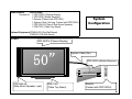
3.
Model Number
PDP-5030HD
Consists of 1 PDP-503PU (Plasma Dispay)
1 PDP-R03U (Media Receiver)
1 Remote (Packed with PDP-R03)
1 System Cable (3m long, Packed with PDP-R03U)
1 PDP-S06-LR (Pair of Side Mount Speaker)
1 PDK-TS01 (Table Top Stand)
System
Configuration
Optional Equipment PDWB-5003 (Flat Wall Mount)
PWM-503 (Tilt Wall Mount)
50 inch
PDP-503PU (Plasma Display)
50”
System Cable (3m)
PDP-R03U (Media Receiver)
STANDBY
POWER
STANDBY/ON
PDP-S06-LR
(Side Mount Speaker / pair)
PDK-TS01
(Table Top Stand)
PLASM A DISPLAY SYSTEM
INPUT
+
-
DOWN
UP
CHANNEL
VOLUME
Remote
(Packed with PDP-R03U)
4.
Model Number
PDP-4330HD
Consists of 1 PDP-433PU (Plasma Dispay)
1 PDP-R03U (Media Receiver)
1 Remote (Packed with PDP-R03)
1 System Cable (3m long, Packed with PDP-R03U)
1 PDP-S09-LR (Pair of Side Mount Speaker)
1 PDK-TS01 (Table Top Stand)
System
Configuration
Optional EquipmentPDP-S08 (Under Mount Speaker)
PDWB-5003 (Flat Wall Mount)
PWM-503 (Tilt Wall Mount)
43 inch
PDP-433PU (Plasma Display)
System Cable (3m)
43”
PDP-R03U (Media Receiver)
STANDBY
POWER
STANDBY/ON
PDP-S09-LR
(Side Mount Speaker / pair)
PDK-TS01
(Table Top Stand)
PLASM A DISPLAY SYSTEM
INPUT
+
-
DOWN
UP
CHANNEL
VOLUME
Remote
(Packed with PDP-R03U)
5.
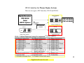
DVI-I interface for Plasma Display Systems
There are two types of DVI interface; DVI-D and DVD-I.
Media Receiver
PDP-R03U
Only!
HDCP System
PDP-5030HD
PDP-4330HD
No Connection
Possible
(Yellow square)
6.
Supplied cable must be used.
Y-Drive
Heat Sink
Trap switch must be closed to
operate with back off.
AC Trap
Switch
Caution!
See Page 27 in this guide
or page 85 in the service manual.
X-Drive
Heat Sink
Caution
Due to fan less
operation the X &
Y drive PCB's have
heat sinks attached
and must be
reinstalled if PCB
needs replacement.
7.
Higher luminance is realized by changing the cell structure.
2. Technical explanation on the new features.
- Higher luminance and contrast -
PDP-5030HD
PDP-4330HD
8.
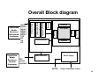
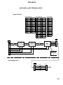
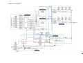
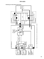
Overall Block diagram
Memory
Address
PDP panel
Y Drive
Drive controller
Scan
X Drive
Memory Controller
Data Controller
Input From
Media
Receivers
System
Connector
Data Interface
Input From
Media
Receivers
DVI System
Connector
R(A)0~7
G(A)0~7
B(A)0~7
R(B)0~7
G(B)0~7
B(B)0~7
CLK
HD
VD
DE
Address
Panel controller
Power supply
PDP
module
CONTROL
6V/15V
Power On/Standby control
9.
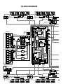
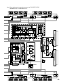
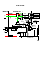
BLOCK DIAGRAM
Driver
IC
Driver
IC
Driver
IC
Driver
IC
VADR2
CLK/LE
ADR CONNECT A
ASSY
AA1
CLAMP
Driver
IC
Driver
IC
Driver
IC
Driver
IC
VADR2
IC6501
Buffer IC
Driver
IC
VADR2
Driver
IC
Driver
IC
Driver
IC
CLK/LE
ADR CONNECT B
ASSY
AB1
CLAMP
CLA1
Driver
IC
Driver
IC
Driver
IC
IC6601
Buffer IC
Driver
IC
VADR2
BGA1
CLAMP A
ASSY
Q6706 - Q6711
VADR Gen.
BRIDGE A
ASSY
K2
K1
ADR RESONANCE
ASSY
SAA3
ADR_CO
+60
SUB ADDRESS A
ASSY
SAA1
D8
D9
D16
D10
D1
+12V
V+5V
V+5V_STB
SCAN (B) ASSY
(UPPER)
THERMAL
SENSOR
ASSY
IC5
VCC_VH
IC6201
ADD
PSUS
SEL_PULSE
V+3V
+12V
DC/DC Conv.
Module
TE1
D11
Y DRIVE ASSY
DIGITAL VIDEO
ASSY
KL_U0:2
VC_VF+ VC_VF- V_OFS VCC_VH V_IC5V
D7
D18
DC/DC Conv.
Block
VCP
Y4
Y-SUS
MASK
Block
IC5
VCC_VH
IC6204
ADD
SEL_PULSE
IC2206
Pulse Module
+15V
XDRV_SIG
ADL_LE_UL
ADL_LE_DL
Y1
+5V +15V VSUS
PSUS
IC1703
XY Drive
Sequence Pattern
Gen.
Drive
Signal
D6
VSUS
V+2V
YDRV_SIG
SCAN_SIG
IC5
VCC_VH
IC6203
ADD
SEL_PULSE
V+3V
X180 V+3V_IC
Clock
V+2V_IC V+5V_STB
Gen.
Logic
Block
+Reset Block
IC5
VCC_VH
IC6206
ADD
SEL_PULSE
SCAN
VCC_VH
V_IC5V
D4
V+3V
Y2
IC5
VCC_VH
IC6205
ADD
SEL_PULSE
V+2V
+12V
V+3V
IC5
VCC_VH
IC6202
ADD
SEL_PULSE
IC1301 (IC31 L)
Sub-Field Conv.
for Left with Field Memory
VCP
D15
+5V +15V VSUS
Y-SUS
MASK
Block
Y3
IC2204
Pulse Module
Drive
Signal
V+3V_I
SCAN (A) ASSY
(LOWER)
D14
V+2V_I
+15V
VCC_VH
V_IC5V
IC5
VCC_VH
IC6001
ADD
SCAN
SEL_PULSE
IC1401 (IC31 R)
Sub-Field Conv.
for Right with Field Memory
Soft-D
Block
D2
Y5
IC5
VCC_VH
IC6002
ADD
SEL_PULSE
ADCLK_DR
BA2:9
VC_VF+ VC_VF- V_OFS
BB2:9
V+3V
Scan Signal
IC5
VCC_VH
IC6003
ADD
SEL_PULSE
SAA2
Offset
Block
GA2:9
IC1191
Flash
ROM
V+5V_STB
PSUS
V_IC5V
IC5
VCC_VH
IC6004
ADD
SEL_PULSE
Photo Coupler
Block
Y6
GB2:9
V+3V
IC1207
Module
UCOM
IC5
VCC_VH
IC6005
ADD
SEL_PULSE
TXD/RX
RA2:9
IC1101
Panel UCOM
RB2:9
TXD0/RX0
RE
LED_SIG
I2
IC5
VCC_VH
IC6006
ADD
SEL_PULSE
PSUS
D17
D12
D3
D13
FRONT KEY
ASSY
FRONT KEY CONN
ASSY
SW21
KL21
KL22
SUB ADDRESS B SAB1
ASSY
IR (P)
ASSY
SAB2
+60
RE1
CLAMP B
ASSY
BRIDGE C
ASSY
CLB1
ADR_CO
SAB3
ADR RESONANCE
ASSY
K1
K2
Q6706 - Q6711
VADR Gen.
BGC1
VADR2
CLAMP
AD1
CLAMP
ADR CONNECT D
ASSY
CLK/LE
IC6901
Buffer IC
VADR2
VADR2
ADR CONNECT C
ASSY
AC1
CLK/LE
IC6801
Buffer IC
VADR2
10.
Driver
IC
Driver
IC
Driver
IC
Driver
IC
Driver
IC
Driver
IC
Driver
IC
Driver
IC
Driver
IC
Driver
IC
Driver
IC
Driver
IC
Driver
IC
Driver
IC
Driver
IC
Driver
IC
Note : When ordering service parts, be sure to refer to "EXPLODED VIEWS
and PARTS LIST" or "PCB PARTS LIST".
Driver
IC
Driver
IC
Driver
IC
VADR2
Driver
IC
Driver
IC
Driver
IC
Driver
IC
CLK/LE
ADR CONNECT C
ASSY
AC1
Driver
IC
Driver
IC
VADR2
IC6801
Buffer IC
Driver
IC
Driver
IC
VADR2
Driver
IC
Driver
IC
Driver
IC
CLK/LE
ADR CONNECT D
ASSY
AD1
CLAMP
Driver
IC
Driver
IC
VADR2
IC6901
Buffer IC
CLAMP
BGB1
CLB1
BRIDGE B
ASSY
K3
CLAMP B
ASSY
SW POWER SUPPLY MODULE
SW POWER SUPPLY Block
V MID CLAMP Block
RC101
+13.5V
-9V T101
+6.5V
CLAMP
Switching
Q115
M111
Switching
Q119
+15V
T103
NEUTRAL
Switching Q112
Switching
Q117
+12V T102
LIVE
T104
T105
CLAMP
RL101
PRIMARY
T105
SECONDARY
VSUS_CONT
M114
VM1
P2
VSUS
+15V
VSUS
+13.5V
P5
-9V
+15V
STB5V
VADR
+12V
P1
STB5V
STB5V
+6.5V
+13.5V
-9V
P7
P6
LIVE
P3
NEUTRAL
AC IN
X DRIVE ASSY
P4
X1
+5V
AUDIO AMP ASSY
VCP
Drive
Signal
IC3200
Pulse
Module
X_SUS
MASK
IC4201
EEPROM
(EDID)
MR INTERFACE
ASSY
L
R
L
R
IC5202
+5V
V_RN +15V
Volume & Tone
& Balance
I2C
Interface
• Scalling
• Gamma
IC5201
SRS & Focus
A24
TMDS
Receiver
L, R
IC4204
(Sil861)
TMDS Receiver
+Reset
Pulse
Block
Logic
Block
+12V
Copy Guard
Release
FOCUS
SRS
R3
+12V
L, R
IC4203
EEPROM
(HDCP KEY)
P_SUS
R23
R26
R21
R2
X3
VSUS +15V
DC/DC
Conv.
Block
X CONNECTOR (A) ASSY
POWER (RELAY)
+5V
X2
R27
+15V
VSUS +15V
VCP
IC3201
Pulse
Module
X_SUS
MASK
IC5002
A21
R24
V+5V_DIG
Drive
Signal
+13.5V
L, R
IC4011
I/O Expander
KEY1
P_SUS
+12V
IC5001
Reg.
KEY2
X4
LED_SIG
TXD/RXD
SR_UP
R11
L1
LED
ASSY
TRAP SW
R22
L, R
V+5V_ST
AUDIO_SIG (L/R)
V+5V_ST
TMDS with HDCP
A22
SR_DW
X CONNECTOR (B) ASSY
Power Amp.
I2C_BUS (SCL/SDA)
SP TERMINAL
ASSY
System Cable Connector
SP21
SP OUT
K3
BRIDGE D
ASSY
CLAMP A
ASSY
BGD1
ADR CONNECT B
ASSY
VADR2
Driver
IC
Driver
IC
Driver
IC
Driver
IC
CLA1
CLAMP
AB1
CLK/LE
Driver
IC
Driver
IC
IC6601
Buffer IC
Driver
IC
Driver
IC
VADR2
AA1
VADR2
Driver
IC
CLAMP
ADR CONNECT A
ASSY
Driver
IC
Driver
IC
Driver
IC
CLK/LE
Driver
IC
Driver
IC
IC6501
Buffer IC
Driver
IC
Driver
IC
VADR2
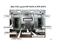
11.
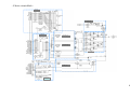
Main PCB Layout PDP-503PU & PDP-433PU
Address Modules
Resonance Assy
Y-Drive
X-Drive
Power Supply
V-Mid Clamp
Scan Modules
Audio Amp
Address Modules
MR Interface
Resonance Assy
Digital Video
12.
PDP-433PU
AUDIO AMP and SP TERMINAL ASSYS
AUDIO AMP ASSY
IC5202 (CXA2021S)
IC5201 (NJM2193L)
No. Voltage (V) No. Voltage (V)
IC5002 (LA4628)
No. Voltage (V) No. Voltage (V)
No. Voltage (V)
1
5.9
12
5.25
1
5.95
16
11.91
1
1.6
2
0
13
1.73
2
5.94
17
0
2
7.5
3
5.95
14
5.95
3
5.84
18
0
3
0
4
5.94
15
5.92
4
5.98
19
5.98
4
3.37
5
5.98
16
5.91
5
5.98
20
5.91
5
2.29
6
6.02
17
5.93
6
5.97
21
5.97
6
1.6
7
6.02
18
5.92
7
5.98
22
5.98
7
1.97
8
7.38
19
5.94
8
5.98
23
5.98
8
7.3
9
5.95
20
5.95
9
5.98
24
5.98
9
7.3
10
1.55
21
11.91
10
5.97
25
5.97
10
0
11
5.24
22
5.9
11
5.97
26
5.98
11
7.3
12
5.98
27
5.98
12
0
13
5.96
28
5.84
13
7.3
14
5.98
29
5.94
14
15
15
0
30
5.95
A22
J5003
A24
4
6
L
R
22
IC5202
14
(CXA2021S)
1 Audio Pre-Amp. 9
11
7
8
11
12
13
14
R+
8
CN5001
12
L
R
IC5201
19
(NJM2193L)
Focus & SRS
1 Audio Processor 12
30
17
L
1
R
6
18
IC5002
(LA4628)
Audio
Power Amp.
4
R–
9
L+
11
L–
13
2
3
5
6
5
STB SW
A_MUTE
SCL
SDA
12 watt X 2
Audio Amp
IC
FOCUS
SRS
SP TERMINAL ASSY
SP21
CN5302
2
3
5
6
R+
L5301
ATF1206
CN5301
4
R–
3
L+
1
L–
SPEAKER
TERMINAL
2
L5352
ATF1206
13.
DIGITAL VIDEO ASSY
MR INTERFACE
ASSY
DIGITAL VIDEO ASSY
3.3V
2.5V
3.3V
RGB 2 phase 8 bit
IC1301 (IC31 L)
(PD6358)
DRAM
Address Data
IC1401 (IC31 R)
(PD6358)
DRAM
Address Data
ADR CONNECT A - D
Assy (Left section)
Line
Buffer
IC4204
SiI861
Address BUS
Data BUS
3.3V Control Signal
RESET
APD MUTE
EXD TXD
3.3V → 5.0V
RST2
EXD RXD
EXT_TXD
RST PU
5.0V → 3.3V
Reset IC
EXT_RXD
IC4005
Expander
RXDO
TXDO
AND
OR
STB5V
IIC BUS
IC1207
(M30624FGAFP)
Module Microcomputer
A_SCL, A_SDA
EEP
ROM
DCC_PD
5V
RXDO
IC4011
Expander
ADR
RESONANCE
Assy
ADR_K_EMG
5V
STB5V
To
MR
X DRIVE Assy
PC_VIDEO
RXD
BUSY
REQ_PU
CN1201
Address
Resonance
Control
DEW DET
AND
IC1101
(HD64F2328VF)
Panel Microcomputer
ADR K PD U
ADR K PD D
HD
VD
Y DRIVE Assy
Sustain
Control
ADR PD
3.3V
IC1703 (IC23)
(PE5064)
STOPB
IC1191
Flash ROM
APLR
Reflesh-rate
Det.
ADR CONNECT A - D
Assy (Right section)
3.3V
VD 31
VD
HD
DE
CLK
Panel W/B ADJ.
Hour/Pulse meter
pn
5V
3.3V
2.5V
STB5V
DC/DC
Converter
Block
OR
TXDO
STB5V
Digital RGB
12V
AC_OFF
PD_TRIGGER
DIG. ADR. PD
Reset IC
RELAY
RESET
TEMP1
WE_PN
To
AUDIO
Assy
THERMAL
SENSOR
Assy
Sync & Clock Signals
SW POWER SUPPLY Module
14.
Digital Video Assembly
The 2 phase 8 bit RGB signal, sync, data and clock lines input the
Digital Video Assembly from the MR Interface assembly. The signals pass
through the line buffer and into IC1301 and IC1410 (sub-field Data
Generators) where the address data is generated and sent out to the left
section and right section address connectors A-D.
X and Y drive sustain control is preformed by IC1703 and the panel
microcomputer IC1101. The panel microcomputer monitors the
horizontal and vertical drive signals to select the proper refresh rate. The
module microcomputer IC1207 controls the panel microcomputer via
logic lines sent through voltage logic level converters. IC1207 is
controlled by the main microcomputer inside the media receiver. IC1207
functions also include thermal sensor monitoring, dew detection, reset
control and is used not only to switch on the power supply but to also
switch off the power supply should one of the power down detect lines
activate.
15.
- Y drive circuit block Scan logic
Reset pulse gene
Logic Block
Sus pulse gen
Sus pulse gen
Sus mask Block
Detect over current
of 15V or Vcp.
Voffset gene
Detect over current
over voltage of Vofs/
Vh/IC5V.
D-D conv
16.
Y- Drive Block
The Y- Drive PCB receives Scan and Y – Drive signals from the
Digital Video Assembly’s drive sequence generator. Scan signals
are processed by the logic block and sent out to the upper and
lower scan drive assembly’s. The Y – Drive signals ( YSUS up,
YSUS down, YSUS B plus and YSUS ground are also sent to the
logic block. The four signals are sent out in parallel to the upper
and lower sustain pulse generators. The drive signal output from
the sustain pulse generators are controlled by reset, offset and
mask FET’s shown in each block to obtain the Panel Sustain signal
sent to the upper and lower scan drive modules. This module also
contains a DC to DC converter, dew detect and over current detect
circuits.
17.
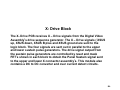
- X drive circuit block -
Sus pulse gen
Logic Block
Sus pulse gen
Sus mask Block
-Reset pulse gen
Detect over current
of 15V or Vcp.
Detect over current
of reset pulse.
Detect over current.
Over voltage of Vrn.
Vrn D-D conv
18.
X- Drive Block
The X- Drive PCB receives X – Drive signals from the Digital Video
Assembly’s drive sequence generator. The X – Drive signals ( XSUS
up, XSUS down, XSUS B plus and XSUS ground are sent to the
logic block. The four signals are sent out in parallel to the upper
and lower sustain pulse generators. The drive signal output from
the sustain pulse generators are controlled by reset and mask
FET’s shown in each block to obtain the Panel Sustain signal sent
to the upper and lower X connector assembly’s. This module also
contains a DC to DC converter and over current detect circuits.
19.
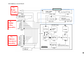
- Sub Address circuit block To
Power
Supply
ADR K power down detection
Detect over current of Vadr line.
1
Detect Stop of Vadr pulse
To
Digital
Video
Assembly
To
Address
Resonance
Assembly
ADR load detect
Detect current load of ADR IC.
Limit the number of adr data pulses.
20.
Sub Address Block
The two Sub Address Circuits are located just above and below the
address driver connect assembly’s ( between B & C connectors ).
See the overall block Diagram for locations. The upper and lower
sub address circuits monitor the current draw of the 60 volt supply
to the address drivers. If a small amount of current draw is detected
(more than normal) a signal is sent back to the Digital Video
Assembly (ADRK EMG1) as an emergency signal and the Digital
Video Assembly will limit the number of address data pulses in
order to lower the current draw. If the current draw is too large the
address power down signal will be sent to the Digital Video
Assembly (ADRK PD) and the panel will go into power down
condition. (red flashing LED).
21.
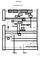
Address resonance/V mid clamp circuit block ADR resonance assy
K2
Vadr(60V)
1
10
19
20
21
22
23
K3- VM*
1
SW
2 DGND
3 ADRGND
4 V MID
5 V ADR
To Bridge/
Clamp assy
22.
Address Resonance & V-Mid Assembly’s
The two Address Resonance circuits are located next to each Sub
Address PCB and the V-Mid circuit is located just to the right of the
power supply PCB. In later production models the V-Mid assembly
will be located on the power supply bracket. These circuits are used
to protect the address driver IC’s in the event of extreme picture
changes. An example would be if the entire picture was alternating
each cell black and white. This causes the IC’s to overheat. The
Digital Video circuit will detect the rapid frequency change in the
addressing signals and will turn on the V-Mid clamp switch. The VMid circuit will take the normally 60 volt address output signal and
lower it by half (30 volts). The voltage will return to normal once the
Digital Video circuit has determined the frequency to be an
acceptable rate.
23.
PDP-433PU
MR INTERFACE ASSY
CN4003 (DVI)
IC4204
TMDS_RXCORE
CONTENT_PROTECTION
SCALING
8bit_DIGITAL
× RGB
TMDS
IC4203
(CONF_ROM)
Q4201, Q4202
(5V ↔ 3.3V
I2C_LEVEL_SHIFT)
Q4005, Q4006
(5V ↔ 3.3V
I2C_LEVEL_SHIFT)
IC4201
(DDC_ROM)
IC4012 (IC2_SW)
6 DDC_SCL
7 DDC_SDA
DDC_SCL
DDC_SDA
14 DDC5V
IC4013
(STB_DET)
Q4014 (REM_CUT)
PMST
IC4010
(NON_SYSTEM_DET)
Q4018 (INV)
C4043
(HPF)
Q4001, Q4002 (I2C_SW)
CN4002 (MDR)
CN4004, CN4005
IC4011
(I/O_EXPANDER)
IC4006 (REM_SLICER)
15 SR_UP
V+5V_DIG
IC4005
(I/O_EXPANDER)
Q4008 (2.5V_REG)
IC4006 (TTL → CMOS CONVERT)
A_SCL
A_SDA
S4001, S4004, etc
(MODEL_INFO)
RXD0
11 M_TXD
IC4006 (BUFF)
TXD0
1 M_RXD
Q4012 (INV)
REM
14 SR_DOWN
IC4008, IC4009 (REM_SW)
Q4007 (BUFF)
SM_POW
5 SM_POW
7 CCKM
8 CSEN2
R4093
R4098
(BIAS)
IC4010 (BUFF)
CCKM
IC4007 (COMPR)
+
SW_TRG
F_KEY1
F_KEY2
Q4011 (DRIVER)
LED_G
LED_R
I2C
Q4401 (BUFF)
10 20
SPL
4 13
SPR
L_CH
Q4402 (BUFF)
R_CH
CN4007
LED_R
LED_G
KEY2
KEY1
REM
CN4401
CN4009
24.
PDP-433PU
PANEL FACILITIES
Plasma Display
STANDBY/ON INPUT
CHANNEL
VOLUME
STANDBY/ON
Power indicator
MAIN POWER button
INPUT button
STANDBY/ON button
CHANNEL
VOLUME
buttons
buttons
Remote control sensor
25.
PDP-433PU
PCB LOCATION
CLAMP A
Assy
ADR CONNECT A
Assy
BRIDGE A
Assy
THERMAL SENSOR
Assy
ADR CONNECT B
Assy
SUB ADDRESS A
Assy
ADR RESONANCE
Assy
SCAN (A)
Assy
Y DRIVE
Assy
ADR CONNECT C
Assy
BRIDGE B
Assy
SW POWER SUPPLY
Module
DIGITAL VIDEO
Assy
ADR CONNECT D
Assy
SCAN (B)
Assy
CLAMP B
Assy
IR (P) Assy
X CONNECTOR (A)
Assy
CLAMP A
Assy
X DRIVE Assy
AUDIO AMP
Assy
FRONT KEY CONN
Assy
FRONT KEY Assy
ADR CONNECT D
Assy
SP TERMINAL
Assy
BRIDGE C
Assy
ADR CONNECT C
Assy
X CONNECTOR (B)
Assy
MR INTERFACE
Assy
ADR RESONANCE
Assy
SUB ADDRESS B
Assy
ADR CONNECT B
Assy
BRIDGE D
CLAMP B
Assy
Assy
ADR CONNECT A
Assy
LED Assy
Rear View
26.
PDP-433PU
DISASSEMBLY
About Detect (Trap) switch
SW Power Supply Module
This unit uses a "Rear Case opened ! detection" system.
Please follow the outline and cautions below.
Outline and caution
In servicing, the media receiver should be connected to the
plasma display. Input signals passing through the media
receiver adopt contents protection by HDCP for copyright
protection.
After removing the rear case do not apply power until the
Detect (Trap) switch has been defeated. The media receiver
and plasma will not power up otherwise.
Detect switch does not detect at the power supply OFF and
the remote control unit wait state. Please close this detect
switch with tape before turning on the power for service
and diagnoses of the plasma display.
1
Remove the Rear Case (P).(Screws × 19)
1
1
×2
×2
1
1
1
×2
1
1
1
1
1
2
3
4
×2
1
1
1 1
1
Remove the IF Earth Metal.(Screws × 2)
Remove four screws.
Remove the SW Power Supply Module.
SW Power Supply
Module
3
3
Rear View
Detect Switch (S2)
4
IF the detect switch has Activated
If the detect switch activates, the front panel LED flashes
by a 300msec period. To release the detect mode cover the
switch with tape then Press the "MENU" key, "ENTER"
key, "POWER" key in that order with the remote control unit.
3 2
×2
IF Earth
Metal
3
This unit powers on and enters the service factory mode
screen. Afterwards, turn off the power with the remote
control unit.
Perform the normal operation afterward.
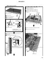
27.
PDP-433PU
5
Insert the SW Power Supply Module into the slit
of Sub Frame L and R.
Slit
MR INTERFACE, AUDIO AMP SP TERMINAL
and DIGITAL VIDEO Assys
1
2
Remove the Rear Case (P). (Screws × 19)
3
4
5
6
Remove the IF Earth Metal (Screws × 2)
Remove the SW Power Supply Module.
(Connector, Screws × 4)
Remove the MR INTERFACE Assy (Connector, Screws × 4)
Remove the SP TERMINAL Assy (Connector, Screws × 2)
Remove the AUDIO AMP Assy (Connector, Screws × 2)
IF Earth
Metal
5
MR INTERFACE
Assy
AUDIO AMP Assy
SW Power Supply
Module
Sub Frame L
Sub Frame R
3
×2
4
6
6
SP TERMINAL
Assy
5
6
4
×4
5
SW Power Supply
Module
7
×2
Remove the DIGITAL VIDEO Assy
(Connector,Circuit Board Spacer × 6)
Diagnosis
7
DIGITAL
VIDEO Assy
28.
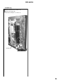
PDP-433PU
Y DRIVE, SCAN (A), (B) Assy
1
Remove the three screws.
7
8
Remove the Rear Case (P). (Screws × 19)
9
Remove the Front Chassis V. (Screws × 5)
Remove the Y DRIVE Assy.
(Connector, PCB Spacer × 3, Screws × 8)
10 Remove the Scan IC Spring (43L) and (43R).
(Screws × 1)
Y DRIVE Assy
Front Case Assy 43 (P)
2
3
4
8
Loosen the rivet.
1
8
×2
×2
8
×3
Remove the Lead Cover (P).
Pull out Flexible Cable.
9
8
8
10
9
8
8
9
9
2
Scan IC Spring (43L)
4
Scan IC Spring (43R)
9
Lead Cover (P)
Rivet
Turn to release the rivet.
3
Lead Cover (P)
To remove, pull out
the Lead Cover (P) with the rivet
before completely removing the rivet.
5
6
11 Flip over the SCAN (A) and SCAN (B) Assemblies.
12 If defective replace the scan IC's.
SCAN (B) Assy
Remove bottom by the fulcrum at the top of Front Case
Assy 43 (P).
Remove the Front Case Assy 43 (P).
Front Case Assy 43 (P)
11
Rear Case
6
Aluminum
Materials
11
The hook on the
Front Case Assy 43 (P) was put between
with Rear Case and aluminum materials.
Scan IC's ×6
SCAN (A) Assy
5
29.
PDP-433PU
X DRIVE Assy
1
2
Remove the Rear Case (P). (Screws × 19)
Remove the X DRIVE Assy.
(Connector, PCB Spacer × 3, Screws × 8)
2
×2
2
2
2
X DRIVE Assy
2
2
×2
30.
PDP-433PU
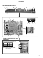
UPPER LAYER SECTION (1)
13
14
13
13
13
14
13
13
2
1
5
4
14
16
15
14
J201
17
12
J202
6
7
8
3
10
11
9
Caution in the MR INTERFACE Assy
Replacement
Set the slide switches in accordance with model
chart when replacing the MR INTERFACE Assy.
PDP-4333P
PDP-433PE
PDP-433PU
S4001
CBIT_1
S4004
CBIT_0
→
←
→
→
→
→
Note 1: When there is not S4004, set only S4001.
Note 2: When there are not S4001 and S4004,
setting is unnecessary.
S4001
(CBIT_1)
S4004
(CBIT_0)
31.
PDP-433PU
UPPER LAYER SECTION (2)
15
PDP-433PU ONLY
17 14
4 15
3
8
7
5
6
18
9
16
13
10
11
12
2
7
P7
P6
P1
P4
P2
P3
P5
100V
SW101
200V
1
Caution!
AC input
Voltage
selector
switch
32.
PDP-433PU
ADJUSTMENT
SERVICE FACTORY MODE
Service factory mode uses an OSD function of the Media Receiver (PDP-R03E or PDP-R03U).
Perform adjustments with the Media Receiver connected to the system.
Remote Control Unit Operation in The Service Factory Mode
Operate the service factory mode with the remote control unit (AXD1463 or AXD1460) .
Please perform the adjustment by operating the following keys.
Remote
Control Key
Function
P + key
One line moves the selection cursor of the adjustment item up.
P – key
One line moves the selection cursor of the adjustment item down.
VOL
+ key
+1 raises a adjustment value
VOL
– key
–1 reduces a adjustment value
5 key
Perform page down (previous page)
∞ key
Perform page up (next page)
2 key
–10 reduces a adjustment value
3 key
+10 raises a adjustment value
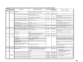
33.
PDP-433PU
How to Enter the Service Factory Mode
Press the "
(POWER)" key (POWER OFF)
System standby state
Confirm that the plasma display and the media receiver turned on together and the
system cable is connected properly.
Perform the following operation by the remote control unit in less than 3 seconds.
• Press the "MENU" key
• Press the "ENTER" key
• Press the "0" key
Press the "Factory" key (Note 1)
Image receiving state
Press the "Factory" key (Note 1)
Service Factory Mode
Page 1/13
General information of the Plasma Display and Media Receiver
Page 2/13 to 9/13
Adjustment and setting item of the Media Receiver
Switch pages
with "5" and "∞" keys.
Page 11/13 to 13/13
Adjustment and setting item of the Plasma Display
Note 1: When using remote control with a {AA5F code} Factory Key
34.
PDP-433PU
General Information of the Plasma Display and Media Receiver
Display example of the first page
1
2
3
4
5
6
7
8
9
10
11
12
13
14
15
16
17
18
1 / 13
CENTER Ve r s i on
OSD Ve r s i on
CV I C Ve r s i on
TTXP Ve r s i on
MON I TOR Ve r s i on
PANEL Ve r s i on
FLASH Ve r s i on
MON I TOR Mode l
Mod e l S e l e c t Ma i n
Mod e l S e l e c t AV
Mod e l S e l e c t MON I TOR
Sen so r e Temp
Cen t e r A cu t ime
RESET
Mon i t o r Ac u t i me
RESET
Pu l s e Ac u t i me
RESET
No.
I NPUT 1 No S I G
MR MA I N E 2 0 0 1 / 0 9 / 2 5 H
MR OSD 2 0 0 1 / 0 9 / 1 0 A
W2 0 0 1 / 0 9 / 1 2 0 9 : 0 0 X2 0 0 1 / 0 9 / 1 2 0 9 : 0 7
V2 0 0 1 / 0 9 / 1 2 0 9 : 1 0
TTX PRG
061
F6 9 1 1 0
- 00
- 05
01
0
4
0
+28
16
H 41 M
OFF
47
H 42 M
OFF
164
OFF
Item
1
Main software version information of the media receiver
2
OSD version information of the media receiver
3
IP/resize IC control software version information of the
media receiver
4
Text microcomputer software version information of the
media receiver
5
Module microcomputer software version information of the PDP
6
Panel microcomputer version information of the PDP
7
Panel flash ROM version information of the PDP
8
PDP model information
Explanation
Reference
01: PIONEER 50 inches, 02: PIONEER 43 inches,
11: SHARP 50 inches, 12: SHARP 43 inches
9
Media receiver model information
10
Media receiver model information
11
PDP destination information
0: All SHARP destinations, Japanese and North America destinations of
PIONEER, 3: European and general destinations of PIONEER
12
Temperature information of panel temperature sensor on
the PDP
This is internal temperature information. This is not establishment
environment temperature.
13
Media receiver accumulation operating time
14
Media receiver accumulation operating time reset
15
PDP accumulation operating time
16
PDP accumulation operating time reset
17
PDP accumulation pulse number
Real accumulation pulse number becomes "indicated value *10,000,000 pulse".
PDP accumulation pulse number reset
Turn the display to [ON] by pressing the "VOL +" key, then it becomes [0]
when pressing the "ENTER" key.
18
Turn the display to [ON] by pressing the "VOL +" key, then it becomes [0H]
when pressing the "ENTER" key.
Turn the display to [ON] by pressing the "VOL +" key, then it becomes [0H]
when pressing the "ENTER" key.
35.
PDP-433PU
Adjustment and Setting Item of the Plasma Display
Display example of the eleventh page
1
2
3
4
5
6
7
8
9
10
11
12
13
14
15
16
17
18
No.
11 / 13
MNTR V5 0 WB
MNTR V6 0 WB
MNTR PC WB
MNTR R H I GH1
MNTR G H I GH1
MNTR B H I GH1
MNTR R LOW1
MNTR G LOW1
MNTR B LOW1
MNTR R H I GH2
MNTR G H I GH2
MNTR B H I GH2
MNTR R LOW2
MNTR G LOW2
MNTR B LOW2
I NPUT1 No S I G
02
01
01
255
255
254
510
509
512
255
255
254
510
511
512
Item
Adjustable Range
Shipping Setting
Storage Place
1
PDP_W/B table selection at VIDEO 50Hz
1 or 2
2
PDP
2
PDP_W/B table selection at VIDEO 60Hz
1 or 2
1
PDP
3
PDP_W/B table selection at PC
1 or 2
1
PDP
4
RED_GAIN of PDP_W/B table 1
0 to 255
Factory adjustment value
PDP
5
GREEN_GAIN of PDP_W/B table 1
0 to 255
Factory adjustment value
PDP
6
BLUE_GAIN of PDP_W/B table 1
0 to 255
Factory adjustment value
PDP
7
RED_OFS of PDP_W/B table 1
0 to 999
Factory adjustment value
PDP
8
GREEN_OFS of PDP_W/B table 1
0 to 999
Factory adjustment value
PDP
9
BLUE_OFS of PDP_W/B table 1
0 to 999
Factory adjustment value
PDP
10
RED_GAIN of PDP_W/B table 2
0 to 255
Factory adjustment value
PDP
11
GREEN_GAIN of PDP_W/B table 2
0 to 255
Factory adjustment value
PDP
12
BLUE_GAIN of PDP_W/B table 2
0 to 255
Factory adjustment value
PDP
13
RED_OFS of PDP_W/B table 2
0 to 999
Factory adjustment value
PDP
14
GREEN_OFS of PDP_W/B table 2
0 to 999
Factory adjustment value
PDP
15
BLUE_OFS of PDP_W/B table 2
0 to 999
Factory adjustment value
PDP
Caution in the PDP W/B (No.4 to 15) adjustment:
Adjustment value is reflected without relation in input signal during adjustment to the actual PDP.
For example, when operate a adjustment value of [MNTR HIGH1] during PAL input, switch to the adjustment value operation of W/B table 1
while displaying PAL in the actual PDP.
This is temporary.
After adjustment, it becomes the W/B table 2 operation in the PAL input after restarted in the normal mode. It becomes an operation of the W/B
table 1 adjustment value after adjustment in the NTSC input.
As for the above example, table selection (No. 1 and 2) becomes the shipping setting.
36.
PDP-433PU
Display example of the twelfth page
1
2
3
4
5
6
7
8
9
10
11
12
13
14
15
16
17
18
12 / 13
ABL V I DEO 6 0 PC
ABL V I DEO 5 0
VOF S ADJ
VSU S ADJ
XSU SB ADJ
XSU SG ADJ
YSU SB ADJ
YSU SG ADJ
No.
Item
I NPUT1 No S I G
118
122
131
128
08
08
08
08
Adjustable Range
Shipping Setting
Storage Place
1
Electric power setting at the PC, VIDEO 60Hz
0 to 255
Factory adjustment value
PDP
2
Electric power setting at VIDEO 50Hz
0 to 255
Factory adjustment value
PDP
3
VOFS voltage setting
0 to 255
Factory adjustment value
PDP
4
VSUS voltage setting
0 to 255
Factory adjustment value
PDP
5
SUS_B timing setting of X drive
0 to 15
Factory adjustment value
PDP
6
SUS_G timing setting of X drive
0 to 15
Factory adjustment value
PDP
7
SUS_B timing setting of Y drive
0 to 15
Factory adjustment value
PDP
8
SUS_G timing setting of Y drive
0 to 15
Factory adjustment value
PDP
Adjustment of these items could result in damage if improperly adjusted. When adjustment is needed, be careful.
Caution in the electric power setting (No. 1 and 2) adjustment:
Adjustment value is reflected without relation in input signal during adjustment to the actual PDP.
For example, when operate a adjustment value of [ABL VIDEO 60 PC] during PAL input, switch to the adjustment value operation of [ABL
VIDEO 60 PC] while displaying PAL in the actual PDP. This is temporary.
After adjustment, it becomes the [ABL VIDEO 50] operation in the PAL input after restarted in the normal mode. It becomes an operation of the
[ABL VIDEO 60PC] adjustment value after adjustment in the NTSC input.
37.
PDP-433PU
Display example of the thirteenth page
1
2
3
4
5
6
7
8
9
10
11
12
13
14
15
16
17
18
12 / 13
V I DEO DR I VE MODE
PC DR I VE MODE
NEGAT I VE MODE
BR I GHT ENHANC E
MASK V FREQ
PATTERN MASK
FULL MASK
No.
Item
I NPUT1 No S I G
00
03
OFF
OFF
50
OFF
OFF
Adjustable Range
Shipping Setting
Storage Place
1
Drive mode selection at VIDEO
0 to 5
0
PDP
2
Drive mode selection at PC
0 to 5
3
PDP
3
Negative positive inversion mode
OFF/ON
OFF
PDP
4
Bright enhance
OFF/ON
OFF
None
5
Refresh rate at mask signal generation
50/60/70
–
None
6
Pattern mask signal generation
OFF/
OFF
PDP
7
Full mask signal generation
OFF/
OFF
PDP
Caution in the mask (generation test signal screen in the PDP inside) signal generation:
• A pattern mask and a full mask can use only either.
Therefore, turn full mask OFF when using a pattern mask. Also turn pattern mask OFF when using a full mask.
• A pattern mask and a full mask are test signal screens occurring together in the PDP inside. Therefore, in the mask signal generation, it
cannot acept video inputting from OSD and the outside.
When release mask setting or change of each setting or perform the confirmation of the adjustment or external input signal, perform key
operation of the main unit button or the remote control unit.
38.
PDP-433PU
ADJUSTMENT REQUIRED WHEN THE SET IS REPAIRED OR REPLACED
Y DRIVE Assy
SW POWER SUPPLY Module
When replaced
When repaired
No adjustment required.
1. VOFS/VH/IC5V voltage adjustment
2. Timing adjustment of pulse module
DIGITAL VIDEO Assy
When replaced
When repaired
1. SUSB ground timing adjustment
2. Panel white balance adjustment
No adjustment required.
When replaced
X DRIVE Assy
• Remove IC1204 (24LC04(1) SN-TBB) from the former PC
Board to replace, and install it to the new PC Board.
When repaired
1. VRN voltage adjustment
2. Timing adjustment of pulse module
MR INTERFACE Assy
1. Remove IC4201 from the former PC Board to replace, and
install it to the new PC Board.
2. Set slide SW according to page in this manual or page 22 in the service manual.
When replaced
1. SUSB ground timing adjustment
2. Panel white balance adjustment
SW POWER SUPPLY
Module
Y DRIVE
Assy
X DRIVE
Assy
DIGITAL VIDEO
Assy
MR INTERFACE
Assy
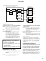
Fig. 1 PC Board Location (rear side view)
39.
PDP-433PU
ADJUSTMENT
VOFS/VH/IC5V Voltage Adjustment
Input Signal
Adjusting Point
Adjusting Method
VOFS (Offset voltage) adjustment
Method 1
1. Write down a adjustment value of VOFS ADJ in the factory mode.
2. Set this adjustment value to center (128).
3. Adjust VR2701 so that the voltage between K2701 (VOFS) and K2703 (SUS GND) becomes
45V.
4. Return it to the value that wrote down a adjustment value of V-OFFSET in step 1.
Method 2
1. Read the adjustment value of VOFS ADJ in the factory mode.
2. Adjust VR2701 so that the voltage between K2710 (VOFS) and K2703 (SUS GND) becomes
following voltage ± 0.5V.
Input
Command
VR2701 (VOFS)
(Y DRIVE Assy)
White 100%
DAC
Output
Setting
Voltage
Input
Command
DAC
Output
Setting
Voltage
VOF000
0.4
25
VOF134
2.599212598
45.94488
VOF006
0.4984375
25.9375
VOF141
2.71496063
47.04724
VOF013
0.61328125
27.03125
VOF147
2.814173228
47.99213
VOF019
0.71171875
27.96875
VOF153
2.913385827
48.93701
VOF026
0.8265625
29.0625
VOF160
3.029133858
50.03937
VOF032
0.925
30
VOF166
3.128346457
50.98425
VOF038
1.0234375
30.9375
VOF172
3.227559055
51.92913
VOF045
1.13828125
32.03125
VOF179
3.343307087
53.0315
VOF051
1.23671875
32.96875
VOF185
3.442519685
53.97638
VOF058
1.3515625
34.0625
VOF191
3.541732283
54.92126
VOF064
1.45
35
VOF198
3.657480315
56.02362
VOF070
1.5484375
35.9375
VOF204
3.756692913
56.9685
VOF077
1.66328125
37.03125
VOF211
3.872440945
58.07087
VOF083
1.76171875
37.96875
VOF217
3.971653543
59.01575
VOF090
1.8765625
39.0625
VOF223
4.070866142
59.96063
VOF096
1.975
40
VOF230
4.186614173
61.06299
VOF102
2.0734375
40.9375
VOF236
4.285826772
62.00787
VOF109
2.18828125
42.03125
VOF242
4.38503937
62.95276
VOF115
2.28671875
42.96875
VOF249
4.500787402
64.05512
VOF122
2.4015625
44.0625
VOF255
4.6
65
VOF128
2.5
45
The symptom is case of mis-adjustment
If the VOFS Voltage adjustment is not performed properly, dots like blinking luminance points
appear. If deviated greatly from the right adjustment point, panel will light white.
VR2703 (VH)
(Y DRIVE Assy)
VH (voltage for scan IC) Adjustment
Adjust so that the voltage between K2716 (VH) and K2720 (PSUS) becomes 103V ± 0.5V.
PSUS (=GNDH) is a floating GND and the electric potential is different from that of chassis
GND. Be sure not to short-circuit PSUS (=GNDH) and another GND, because that may
damage the unit.
The symptom is case of mis-adjustment
If the VH adjustment is not performed properly, dots like blinking luminance points appear. If
deviated greatly from the right adjustment point, panel will light white.
VR2702 (IC5V)
(Y DRIVE Assy)
IC5V Adjustment
Adjust so that the voltage between K2707 (IC5V) and K2720 (PSUS) becomes 5.0V ± 0.1V.
PSUS (=GNDH) is a floating GND and the electric potential is different from that of chassis
GND. Be sure not to short-circuit PSUS (=GNDH) and another GND, because that may
damage the unit.
Note : Be sure to measure between specified test points.
40.
PDP-433PU
Sustain Pulse Waveform Adjustment
Adjusting Point
Input Signal
REF_DIG mode
in Factory mode
White 100%
XSUSB ADJ
YSUSB ADJ
Adjusting Method
X-SUS-B, Y-SUS-B Adjustment
Set to the indicated value with the remote control unit.
(Refer to "Timing adjustment of control signal of X and Y Drive Assys".)
VRN Voltage Adjustment
Adjusting Point
Input Signal
White 100%
VR3701 (VRN)
(X DRIVE Assy)
Adjusting Method
VRN (minus reset voltage adjustment)
Adjust so that the voltage between K3707 (VRN) and K3702 (SUS-GND) becomes
-280V ± 1.0V.
Panel White Balance Adjustment
Input Signal
Adjusting Point
Adjusting Method
Adjust the parameter in the OFFSET-DIGITAL of factory mode as follows;
PANEL R-HIGH
PANEL B-LOW
In this time, dispay uses the mask (MASK04) of factory mode.
Reference : Adjustment values using the Media color-difference meter (A-100)
MASK Left Side
MASK Right Side
x
294
293
y
303
294
∗ When performing the various adjustments by RS-232C control, execute a "DM0" command (release the limit of pulse number)
beforehand.
After the adjustment completion, execute a "DM 3" command (Limit of pulse number: 64%, shipping state)
41.
PDP-433PU
Timing Adjustment of X and Y DRIVE Assys Control Signal
Purpose
• Pulse module loads in DRIVE Assy is one of heat measures of DRIVE Assy. Adjust the drive timing of the pulse module
driving parallel with VR.
• Pulse module has each peculiar delay time. Readjustment is necessary when replacing the pulse module in the X and
Y DRIVE Assys.
Adjustment Method
CR delay circuit is each inserted on signal path of four control signals (SUS-U, SUS-B, SUS-D, SUS-G) driving
the pulse module.
Quantity of delay can adjust pulse module of one side with VR.
Adjust VR while measuring a waveform of the pulse module, and match timing.
Adjustment VR
X DRIVE
SUS-U
VR3203
SUS-D
VR3202
SUS-B
VR3201
SUS-G
VR3200
Y DRIVE
VR2204
VR2203
VR2202
VR2201
Test pin for adjustment and measurment
Pulse Module
X DRIVE
Upper
Lower
SUSOUT
K3105
K3106
SUS-U
K3200
K3204
SUS-D
K3108
K3205
Y DRIVE
Upper
Lower
K2212
K2203
K2220
K2224
K2207
K2225
Adjustment Procedure
Power ON
Black Mask Screen
Measuring points of waveform
are refered to next page.
Display a SUSOUT waveform
Coarse adjustment of
SUS-U, SUS-B, SUS-G
Display a SUS-D waveform
SUS-D adjustment
Adjust the waveform to 20-25ns.
Display a SUS-U waveform
SUS-U adjustment
Adjust the waveform to 20-25ns.
Power OFF
Adjust VR resistance value
of SUS-B and SUS-G to match
VR resistance value of SUS-D
within ± 2Ω.
Power ON and
display a SUS-D waveform
SUS-D readjustment
Adjust the waveform to 20-25ns.
Display a SUS-U waveform
SUS-U readjustment
Adjust the waveform to 20-25ns.
Power OFF
Adjust VR resistance value
of SUS-B and SUS-G to match
VR resistance value of SUS-D
within ± 2Ω.
Power ON and display a SUSOUT
waveform
Compare waveforms,
Should look almost
the same?
No
Yes
Adjustment end
42.
PDP-433PU
Measuring Waveform of Pulse Module Timing Adjustment
Timing adjustment of the pulse module control signal adjusts with the sustain pulse of eighth pulse (X DRIVE) and
the ninth pulse (Y DRIVE) from the back of 6SF.
Measuring point of waveform
Y DRIVE SUSOUT waveform
1SF
X DRIVE SUSOUT waveform
2SF 3SF 4SF 5SF 6SF 7SF
1SF
1ms/div
Magnify 6SF block
2SF 3SF 4SF 5SF 6SF 7SF
1ms/div
Magnify 6SF block
CH1 : Y SUSOUT Under (K2203), 50V/div
CH2 : Y SUSOUT Upper (K2212), 50V/div
CH4 : YPR-U1 (K2038)- Trigger, 5V/div
Trigger : 2msec delay
5µs/div
Use this sustain pulse
and adjust.
CH1 : X SUSOUT Under (K3106), 50V/div
CH2 : X SUSOUT Upper (K3105), 50V/div
CH4 : YPR-U1 (K2038)- Trigger, 5V/div
Trigger : 2msec delay
5µs/div
Use this sustain pulse
and adjust.
• Perform adjustment of waveform with a black mask screen.
• It is easy to adjust when turned field AB offset to OFF (RS-232C
command: OCN) in adjustment.
Note:
• Sampling rate of oscilloscope sets it more than 500MS/s in order
to perform ns order adjustment.
• Collecting calibration of probe before adjustment.
When looking at drive Assy unit waveforms, measure at the
fourth sustain pulse from the back except for a large width sustain
pulse.
Therefore, when measured both waveforms of the X and Y drives
together, it becomes the sustain pulse of 8 and 9 pulses from the
back.
• Connect GND of probe measuring waveform to SUSGND terminal
by all means.
• Precise waveform is not displayed, and an adjustment gap may
occur, make sure to GND properly.
Waveform coarse adjustment
Measure the SUSOUT waveform
When there is a gap with waveform of CH1 / CH2 of the part which
is enclosed in the following circle, adjust required VR to overlap the
waveforms.
1ms/div
Magnify the adjustment waveform
Adjust with SUS-B
500ns/div
Adjust with SUS-U
CH1 : Y SUSOUT Under (K2203), 50V/div
CH2 : Y SUSOUT Upper (K2212), 50V/div
CH4 : YPR-U1 (K2038)- Trigger, 5V/div
Trigger : 2msec delay
Adjust with SUS-G
43.
PDP-433PU
SUS-D Adjustment (Y DRIVE)
SUS-U Adjustment (Y DRIVE)
1ms/div
Magnify 6SF block
1ms/div
Magnify 6SF block
5µs/div
5µs/div
Magnification
Magnification
1ms/div
Magnify 6SF block
1ms/div
Magnify 6SF block
500ns/div
200ns/div
Magnification
Magnification
1ms/div
Magnify 6SF block
1ms/div
Magnify 6SF block
Upper PM
Lower PM
20 - 25ns
Caution:
Not absolutely mistaking upper
and lower of waveform.
10ns/div
CH1 : Y SUS-D Under (K2225), 50V/div
CH2 : Y SUS-D Upper (K2207), 50V/div
CH4 : YPR-U1 (K2038)- Trigger, 5V/div
Trigger : 2msec delay
20 - 25ns
Upper PM
Lower PM
10ns/div
CH1 : Y SUS-U Under (K2224), 50V/div
CH2 : Y SUS-U Upper (K2220), 50V/div
CH4 : YPR-U1 (K2038)- Trigger, 5V/div
Trigger : 2msec delay
Waveform Confirmation in Adjustment completion
Measure the SUSOUT waveform
Confirm it to waveform of CH1 / CH2 of the part which enclosed in
the following circle whether there is not a large gap.
(A gap of the quantity that shifts 20nS and adjusted remains.)
1ms/div
Magnify the adjustment waveform
500ns/div
CH1 : Y SUSOUT Under (K2203), 50V/div
CH2 : Y SUSOUT Upper (K2212), 50V/div
CH4 : YPR-U1 (K2038)- Trigger, 5V/div
Trigger : 2msec delay
When adjust in the power supply ON state, change so that the
quantity of gap that adjusted by temperature-rise of the pulse
module becomes small.
Therefore, perform high power OFF (RS-232C command: DRF)
except measurement time of waveform when adjusts, and
adjustment error by temperature-rise does not occur.
44.
PDP-433PU
SUS-B Ground Timing Adjustment
It is necessary to adjust when replacing the X or Y DRIVE Assy and the pulse module.
Measurement point and method
Measurement point of waveform of X and Y DRIVE Assy in timing adjustment is test pin of SUSOUT of the pulse module of
bottom of the main unit.
X DRIVE Assy : K3106 Y DRIVE Assy : K2203
Measurement screen : Black mask (PC 60Hz)
The measurement is easy to perform when turns field AB alternation to OFF. (RS-232C command: OCN)
Measure a sustain pulse of the fifth pulse (X DRIVE) and the fifth pulse (Y DRIVE) from the back of the fourth FS, and
adjust. In the start section of this sustain pulse, waveform has inflection point with the timing when SUS-B becomes ON.
Adjust so that the voltage of this inflection point is the nearest to 140V and do not become less than 140V.
Adjustment parameter
X DRIVE: XSUSB (RS-232C command : XSB)
Y DRIVE: YSUSB (RS-232C command : YSB)
Note:
• Connect GND of probe measuring waveform to SUSGND terminal by all means.
• Precise waveform is not displayed, and an adjustment gap may occur that does not collect GND properly.
Waveform in the measurement
Rst
1SF
2SF
3SF 4SF
5SF
1ms/div
Magnify 5FS block
CH1 : Y SUSOUT (K2203), 50V/div
CH2 : X SUSOUT (K3106), 50V/div
CH4 : YPR-U1 (K2038)- Trigger, 5V/div
Trigger : 2msec delay
5µs/div
Measure a waveform of this section and adjust.
G
N
O
K
Magnify the fourth pulse sustain pulse (XSUSOUT waveform) from the back of the above waveform.
100nsec/div
140V Line
100nsec/div
140V Line
GND
50V/div
This broken section moves by
changing the adjustment
parameter.
50V/div
Become less than 140V.
→ NG
45.
PDP-433PU
Y DRIVE Assy
X DRIVE Assy
K2720
(PSUS)
K2716
(VH)
K2218
(1/2 VSUS)
K2215
K2217
(SUS_B) (SUS_U)
K2214
(SUS_G)
K2717
(VH CONT)
K3214
(SUSGND)
K3708
(VRN_OVP)
K3213
(1/2VSUS)
K3702
(SUS. GND)
K3707
(VRN)
K2216
(SUS_D)
VR3701
(VRN. ADJ)
K2227
(SUS_D)
K3705
VRN UVP)
K3701
(VSUS)
K3205
(SUS_D)
K2715
(YDC_DC_PD)
K2226
(SUS_U)
K3703
(SUS. GND)
K2718
(VH UVP)
K3704
(VRN. CNT)
K3204
(SUS_U)
VR2703
(VH_ADJ)
K2212
(SUSOUTB)
K2719
(VH OVP)
K2222
K2703
(SUSGND)
K2702
(VSUS)
VR2701
K2710
(VOFS)
K2011
K2010
K2013
K2009
K2005
K2003
K2002
K2001
K2004
K2205
K2708
(VOFS)
K2705
(SUSGND)
K3106
(SUSOUT_B)
K2709
K2712
(VOFSUVP)
K2211
K2225
(SUS_D)
K3102
(XNR_PD)
K3030
K2050
K2048
K2046
K2045
K2049
K2047
K2044 K2043
(DGND)
K2021
K2008
(YPR_U2) K2012
(DGND)
(PN MUTE)
K2053
(SOFT_D)
K2041 (OFS)
K2040
K2038
(YCP_MSK) (YPR_U1)
K2039 (YSUS_MSK)
K2007
K2037 (YSUS_G)
K2029
(DGND)
K2028 (YSUS_U)
(YSUS_D)
K2006
K2024 (+5V)
VR2204
K2027 (DGND)
(SUS_U_ADJ)
(YSUS_B)
VR2203
K2101
(SUS_D_ADJ)
(DEW_DET)
VR2202
(SUS_B_ADJ)
VR2201
(SUS_G_ADJ)
K2203
(SUSOUTA)
K2704
(VF-)
K3008
(PN_MUTE)
K3021
K3007
K3010
(XNR-U) K3022 K3025
K3015
K3017
(XSUS-MSK) (XCP-MSK)
K3014
(XNR-D1)
K3012
(XSUS-D)
K3203
(1/2VSUS)
K2701
(VF+)
K3018 (XNR-D2)
K3013 (XSUS-G)
K3004 (XSUS-U)
K3003 K3001
(XSUS-B) (+5V)
K3103
(VCP_PD)
VR3203
(SUS-U)
K3108
(SUS_D)
K3104
(+5V)
VR3202
(SUS-D)
VR3201
(SUS-B)
VR3200
(SUS-G)
K3200
(SUS_U)
K2714
(GNDHS)
K3009 K3006
K3011
K3029
K2221
(+15V)
K2707
(IC5V)
K2224
(SUS_U)
K3706
(X DC-DC PD)
K3105
(SUSOUTA)
K2706
(+14V)
K2711
(-8V)
K2713
VR2702
(IC5V_ADJ) (IC5V UVP)
K3201
(SUSGND)
Adjusting Points
46.
PDP-433PU
SHUT DOWN/POWER DOWN DIAGNOSIS BY LED DISPLAY
When internal circuit abnormality and other operation abnormality occurred from this unit, self-diagnose display function by STANDBY/ON
(LED) indicator is loaded.
Each NG point by LED blinking and a PD (power down) point are as follows.
Shut Down
• Operations : When a microcomputer detected abnormality, turn the power supply to OFF.
• LED display : Green blinks
Examples: LED blinks in the DIGITAL-IIC communication NG
Green LED lights
for 200 msec.
Lights out
for 100 msec
Green LED lights
for 200 msec.
Lights out
for 3 sec
Number of
blinks
Name
1
2
3
4
Panel Microcomputer NG
DIGITAL-IIC communication NG
Dew abnormality
Temperature abnormality
How to release the shut down state
Turn the power supply ON by remote control , release from the
shut down state, and turn the power supply ON.
(It is not necessary to turn the AC power OFF.)
Power Down
• Operations : When this unit enters the power down state, the power supply shuts OFF by the protection circuit.
• LED display : Red blinks
* When more than one protection circuit activates, display shows LED's in order to 1st - 2nd.
Examples: LED blinks in the 1st power down = Y-DC/DC CONVERTER, 2nd power down = Y-DRIVE
2nd power-down
information
1st power-down information
Red LED lights
for 200 msec.
Lights out
for 100 msec
Red LED lights
for 200 msec.
Lights out
for 1 sec
Red LED lights
for 200 msec.
Lights out
for 3 sec
Number of
blinks
1
2
3
4
5
6
7
8
Name
Y-DRIVE
Y-DC/DC CONVERTER
X-DC/DC CONVERTER
X-DRIVE
Power supply
Address junction
Address resonance
DIGITAL-DC/DC CONVERTER
How to release the power down state
AC power OFF
↓
Wait for PD LED in the power supply module to shut off
(around 30 seconds).
↓
next, wait for five seconds.
↓
Turn AC power ON.
* After power down release, this unit comes up in the standby state.
47.
PDP-433PU
Block Diagram of Shut Down Signal System
DIGITAL VIDEO ASSY
IC1101
Panel UCOM
DDC_SCL
DDC_SDA
RXD
BUSY
REQ_PU
1
IC1191
Panel UCOM
external Flash ROM
THERMAL SENSOR
ASSY
TXD
CLK
*PU_CE
D18
2
TEMP1 4
2
IC1207
Module UCOM
D3
IC8351
Thermal
Sensor 1
TE1
Y DRIVE ASSY
DEW_DET 3
D6
IC1204
EEPROM
Y2
Moisture
Sensor
CN2002
2
A_SCL
A_SDA
SCL
SDA
D1
SW POWER SUPPLY
MODULE
P2
Expander
MR INTERFACE ASSY
AUDIO ASSY
R3
IC5202
CXA2021S
IC4204
SiI861
IC4005
Expander
IC4011
Expander
MEDIA
RECEIVER
Note: 1 - 4 Shows LED flashing number of times when shut has occurred.
48.
PDP-433PU
Shut down diagnosis
1 Panel microcomputer NG
When a module microcomputer failed in communication with a panel
microcomputer, this NG occurs.
Shut down after OSD display for 30 seconds from the NG detection.
Abnormality to expect
Open / Short of communication line in the Assy
E06
2 DIGITAL-IIC communication NG
When a module microcomputer failed in communication with outside
EEPROM or EXPANDER, this NG occurs.
Shut down after OSD display for 30 seconds from the NG detection.
* However, this communication NG may occur in the standby state.
E06
Abnormality to expect
• Open / Short of communication line in the DIGITAL VIDEO, MR INTERFACE
and AUDIO Assys
• Check points.
DIGITAL VIDEO Assy (D1) ↔ SW POWER SUPPLY Module (P2)
DIGITAL VIDEO Assy (D3) ↔ MR INTERFACE Assy (R3)
MR INTERFACE Assy (R23) ↔ AUDIO Assy (A24)
System Cable
3 Dew detection
When it becomes the dew state in this unit, this NG occurs.
After the dew detection, shuts down immediately.
Abnormality to expect for dew drop
Disconnect a connector CN2002 between Dew drop sensor and Y DRIVE Assy.
4 Temperature abnormality
When temperature of this unit is abnormally high, this NG occurs.
Shut down after OSD display from the NG detection for 30 seconds.
Note: When temperature fell down during indication, return to the normal operation.
E04
Abnormality to expect when it occurs in the environment that is not
high-temperature
• Disconnect a connector between DIGITAL VIDEO Assy (D18) and
temperature sensor 1 (TE1).
Reference
Shut down temperature of each temperature sensor
Sensor Temp 78
1
2
3
4
5
6
7
8
9
10
11
12
13
14
15
16
17
18
1 / 13
CENTER Ve r s i on
OSD Ve r s i on
CV I C Ve r s i on
TTXP Ve r s i on
MON I TOR Ve r s i on
PANEL Ve r s i on
FLASH Ve r s i on
MON I TOR Mode l
Mod e l S e l e c t Ma i n
Mod e l S e l e c t AV
Mod e l S e l e c t MON I TOR
Sen so r e Temp
Cen t e r A cu t ime
RESET
Mon i t o r Ac u t i me
RESET
Pu l s e Ac u t i me
RESET
I NPUT 1 No S I G
MR MA I N E 2 0 0 1 / 0 9 / 2 5 H
MR OSD 2 0 0 1 / 0 9 / 1 0 A
W2 0 0 1 / 0 9 / 1 2 0 9 : 0 0 X2 0 0 1 / 0 9 / 1 2 0 9 : 0 7
V2 0 0 1 / 0 9 / 1 2 0 9 : 1 0
TTX PRG
061
F6 9 1 1 0
- 00
- 05
01
0
4
0
+28
16
H 41 M
OFF
47
H 42 M
OFF
164
OFF
49.
RESONANCE
ASSY
(Lower)
RESONANCE
ASSY
(Upper)
ADR CONNECT
ASSY
(Lower)
ADR CONNECT
ASSY
(Upper)
OR
IC1201-pin 6
OR
IC1201-pin 8
Address PD
Mute
6
D1202 Cathode
AND
7
8
DIGITAL
DC-DC
D1
PD_TRIGGER
DIG_ADR.PD
OR
Y DRIVE ASSY
Y Drive
1
PD Circuit
P2
4
X Drive
X DRIVE ASSY
SW POWER
SUPPLY
MODULE
Note: 1 - 8 Shows LED flashing number of times when power down has occurred.
D17
D16
OR
D12 - D15
OR
D8 - D11
DIGITAL VIDEO ASSY
P3
P4
2
Y DC-DC
5
3
X DC-DC
Y1
X1
OR
Relay
Circuit
PDP-433PU
Block Diagram of Power Down Signal System
50.
PDP-433PU
Function of the various protection circuits (P.D. circuit)
Assy Name
Red LED
Number of
Blinks
1
Kind of P.D.
Circuit
VCP OCP
VOFS OVP
Y DRIVE Assy
VOFS UVP
2
VH OVP
VH UVP
3
X DRIVE Assy
4
P.D. by VOFS undervoltage (= overcurrent)
P.D. by VH overvoltage
P.D. by VH undervoltage (= overcurrent)
VRN OVP
P.D. by VRN overvoltage
VRN UVP
P.D. by VRN undervoltage (= overcurrent)
VCP OCP
P.D. by VCP overcurrent
P.D. by reset circuit overcurrent
P.D. by VSUS overvoltage
VSUS UVP
P.D. by VSUS undervoltage (= overcurrent)
VADR OVP
P.D. by VADR overvoltage
VADR UVP
P.D. by VADR undervoltage (= overcurrent)
15V OVP
5
P.D. by VOFS overvoltage
P.D. by IC5V undervoltage (= overcurrent)
RESET OCP
P.D. by 15V overvoltage
15V UVP
P.D. by 15V undervoltage (= overcurrent)
12V UVP
P.D. by 12V undervoltage (= overcurrent)
6.5V OVP
P.D. by 6.5V overvoltage
6.5V UVP
P.D. by 6.5V undervoltage (= overcurrent)
13.5V UVP
-9V UVP
Remarks
P.D. by VCP overcurrent
IC5V UVP
VSUS OVP
SW POWER SUPPLY
Module
Function
P.D. by 13.5V undervoltage (= overcurrent)
P.D. by -9V undervoltage (= overcurrent)
+B OVP
P.D. by +B overvoltage
+B OCP
P.D. by +B overcurrent
AC200V P.D.
P.D. by AC200V apply
Note 1
PFC module overheat protection
VSUS arc resistance overheat protection
ADR CONNECT Assy
6
ADR.PD
P.D. by disconnecting the connector
RESONANCE Assy
7
ADR.K.PD
P.D. by ICP open and TCP defective
5.0V OVP
P.D. by 5V overvoltage
DIGITAL VIDEO Assy
8
5.0V UVP
P.D. by 5V undervoltage (= overcurrent)
3.3V OVP
P.D. by 3.3V overvoltage
3.3V UVP
P.D. by 3.3V undervoltage (= overcurrent)
2.5V OVP
P.D. by 2.5V overvoltage
2.5V UVP
P.D. by 2.5V undervoltage (= overcurrent)
Reference
OVP : Over Voltage Protect
UVP : Under Voltage Protect
OCP : Over Current Protect
Note 1: AC200V P.D. is not applicable to the PDP-433PE and PDP-433PU models.
51.
Diagnosis of the error point in the various protection circuit (P.D. circuit) operation (Red LED blinks)
Number
P.D. Point in
of
Blinks Operation
1
Y DRIVE
Error Pont
Possible Part of Error
Circuit State
Operation
P.D. Circuit
Y DRIVE Assy
IC2206, IC2214 (Pulse module), IC2203, IC2204,
IC2212, IC2213, IC2213, IC2217, R2209
K2211 Lo
VCP OCP
VOFS D/D CONV. BLOCK (Y DRIVE Assy)
IC2702, IC2709, IC2715
K2712 Lo
VOFS OVP
K2709 Lo
VOFS UVP
K2719 Lo
VH OVP
IC2701, IC2702, IC2709, IC2715
VOFS D/D CONV. BLOCK (Y DRIVE Assy)
Q2211, Q2212, R2277, IC2208, IC2210
2
Y DC DC
VH D/D CONV. BLOCK (Y DRIVE Assy)
IC2712, IC2716
VH D/D CONV. BLOCK (Y DRIVE Assy)
IC2711, IC2712, IC2716
SCAN (A), (B) Assy
SCAN IC
IC5V D/D CONV. BLOCK (Y DRIVE Assy)
IC2704, IC2706, IC2717
SCAN (A), (B) Assy
SCAN IC
IC5V D/D CONV. BLOCK (Y DRIVE Assy)
IC2704, IC2706, IC2717
VRN D/D CONV. BLOCK (X DRIVE Assy)
IC3702, IC3712
4
X DC DC
VRN D/D CONV. BLOCK (X DRIVE Assy)
IC3701, IC3702, IC3712
X DRIVE
5
PS
Drive section (control signal, output elements etc.) in
normal operation
K2718 Lo
7
ADR
ADR K
VH D/D CONV. BLOCK in normal operation
SCAN Assy in normal operation
IC5V D/D CONV. BLOCK in normal operation
IC5V UVP
SCAN Assy in normal operation
K3708 Lo
VRN OVP
K3705 Lo
VRN UVP
Q3122
K3103 Lo
VCP OCP
X DRIVE Assy
IC3200, IC3201 (pulse module), IC3103, IC3104,
IC3106, IC3107, IC3110, IC3113, R3109
Q3122
K3102 Lo
VRN OCP
Drive section (control signal, output elements etc.) in
normal operation
VRN D/D CONV. BLOCK in normal operation
X DRIVE Assy
IC3200, IC3201 (Pulse module)
When P4 connector disconnected, P.D. does not occur
Y DRIVE Assy
IC2206, IC2214 (Pulse module)
When P3 connector disconnected, P.D. does not occur
MX AUDIO Assy
IC8601 (Audio IC)
When P6 connector disconnected, P.D. does not occur
ADDRESS CONNECT A - D Assy,
RESONANCE Assy,
D/D CONV. BLOCK (DIGITAL VIDEO Assy)
ADDRESS CONNECT A~D Assy
RESONANCE Assy
When pin 5 of P2 connector disconnected, P.D. does
not occur
SW POWER SUPPLY Module
When the voltage is not output even if P4, P3 and P6
connectors disconnected
Disconnect D8 - D15 connectors
ADR. PD
TCP damage of IC6704 (ICP), disconnect D16 and
D17 connectors, panel microcomputer is defective,
outside Flash ROM of the panel microcomputer is
defective.
D/D CONV. BLOCK (DIGITAL VIDEO Assy) IC1901
8
VH UVP
X DRIVE Assy
SW POWER SUPPLY Module
6
Drive section (control signal, output elements etc.) in
normal operation
VOFS D/D CONV. BLOCK in normal operation
K2713 Lo
3
Diagnosis Condition
ADR. K. PD
K1901 Lo
5.0V OVP
K1902 Lo
5.0V UVP
D/D CONV. BLOCK (DIGITAL VIDEO Assy) IC1901
K1903 Lo
3.3V OVP
K1904 Lo
3.3V UVP
D/D CONV. BLOCK (DIGITAL VIDEO Assy) IC1901
K1905 Lo
2.5V OVP
K1906 Lo
2.5V UVP
DIGITAL
DC DC
Note: About PS PD
The condition that Red LED blinks five times
(power supply PD)
1 When the internal protection circuit of SW
POWER SUPPLY Module worked
2 When a microcomputer was not able to
identify the PD point
↓
Being careful because the protection circuit
of SW POWER SUPPLY Module cannot
conclude that worked.
52.
PDP-433PU
Block diagram for Power supply section
SW POWER SUPPLY MODULE
AC IN
100 - 240V
Power Factor
Control
ST-BY
Power Supply
STB5V
Y DRIVE ASSY
+B395V
VSUS DC/DC
Converter
VOFS DC/DC
Converter
VOFS
-45V
VH DC/DC
Converter
VH
130V
IC5V, VF12V
DC/DC
Converter
IC5V
VF12V
VSUS
215V
VADR
61V
VADR DC/DC
Converter
6.5V DC/DC
Converter
(6.5V, 13.5V, -9V)
13.5V
-9V
15V DC/DC
Converter
(15V, 12V)
12V
X DRIVE ASSY
VRN DC/DC
Converter
VRN
-280V
DIGITAL VIDEO ASSY
15V DC/DC
Converter
(5V, 3.3V, 2.5V)
5.0V
3.3V
2.5V
Supplementary information
1. Power on/off switch for the large-signal system (SW102)
Function: Only the power for the small-signal system
(15V, 12V, 6.5V, 13.5V, and -9V) is on, and the
power for the large-signal system (VSUS, VADR) is
off.
Usage: Use when only an operational check for the smallsignal system is required.
Supplementary information:
When this switch is to be used, the wires of pin 5
(DIG, ADR, and PD) of the P2 connector of the
power-supply module should be disconnected to
prevent the PD circuit from operating. To turn the
power of the large-signal system off without using this
switch, operation from an external PC through
RS-232C commands "DRF" is basically required. In
this case, the above procedure is not required, as the
PD circuit is muted by software.
Method of power supply ON in the large signal
system OFF state with RS-232C command
1 Confirm that this unit is the standby state.
2 Transmit RS-232C command "DRF."
3 Turn the power supply ON by remote control unit, side key
or command "PON."
∗ When turn the power supply OFF once, return to setting of
large signal system ON.
When turn the power supply ON in the large signal system
OFF, transmit "DRF" command each time.
2. 200V AC power-down switch (SW101)
Function: While 200V AC voltage is applied, operation of the
PD circuit is turned on and off (ON when the switch is
set to 100V AC, and OFF when the switch is set to
200V AC).
Setting:
For the PU model only, the switch is set to 100V,
and for other models, it is set to 200V.
3. Temperature compensation of the VSUS voltage for
the drive system
Function: Control the power supply voltage mentioned above
according to temperature. (Temperature compensation
works so that the voltage is lowered on the lowertemperature side, and is raised on the highertemperature side.)
Purpose: To improve the yield by compensating the temperature
characteristics of the panel.
Supplementary information:
For this model, temperature compensation is performed only for the VSUS voltage, and not for the VOFS
voltage, and it is controlled by software.
4. When a fuse blows
• If a fuse blows, never turn the power on again only after
replacing the fuse. (In most cases, the fuse itself did not have
any problem. So as long as factors of overcurrent have not been
removed, chances of destruction increase every time the power
is turned on. In the worst case, about a dozen parts may be
destroyed.)
• Principally, the whole power-supply module must be replaced.
5. Voltage adjustment of the panel drive
As this model employs the electronic VR system for the VSUS
and VOFS voltages, and as the voltage-adjustment data are stored
in the DIGITAL assembly, voltage adjustment of the panel drive
is not necessary when the power-supply modules are changed.
(For VADR, VH, and VRN, adjustments with semifixed VR
controls are necessary.)
For this model, as the power-supply block has been developed
and designed by an outside vendor, at the point you know which
module is a cause of failure (through diagnosis described
elsewhere in this manual), change the corresponding modules, and
do not diagnose or repair the module.
Similarly, the switches and the semifixed VRs inside the powersupply module must not be adjusted without a special reason.
53.