1
MZ-1 D05
•
SHARP SERVICE MANUAL
CODE: OOZMZ-IDOS/I/E
COlOR DISPLAY UNIT
MODEL
Z-l DOS
PRODUCT OUTLINE
-7
The MZ-ID05 is the 14" calor display unit designed for persona1 computer terminal . tAl.
CC> .
It is driven by three independent video signal inputs of R, G, B, and separate synchronous signal inputs of H
and V. Input signa1s are supplied through the round 8-pin DlN connector.
SPECIFICATION
Input frequency band:
Video signal input circuit:
• Video signal amplifier :
• Vertical oscillator :
• Horizontal oscillator:
• Pincushion distortion
correc;:tor
•
Power rectifier :
• Power stabHzer:
• Demagnetizer :
Display tube :
Display tube size :
Power consumption:
High voltage output :
I Cs :
Transistors:
Diodes :
SCR :
Video signal frequency
3 stages
eR ocsillation
eR oscillation
Supply power :
Cabinet:
Physical dimensions :
Weight:
Input signal cable :
Righ t-tD-left satura ble
reac to r type
Capacitor input
b ridge rectifier
SCR phase con trol
Automatic posistor
12><, 90 degree
deflection
320MAB22
2 1.8 wide x 2 1.1 high
x 33.S diagonal (cm)
•
Video signal input:
•
Synchronous signal
input:
H, V seprate sync hronous signal input
method
Input level of 2.4 to
SVp-p nagetive
polarity
58W
22KV
4 chips
15 pes
35 P'"
Ipc
220V ( 50Hz)
Plastic
36 .4 (w) x 42.5 (d) x
37.0 (h)cm
13.5Kg
Round 8-pin DIN
connector
R, G, B th ree independent inpu t method
Inpu t level of 2.4 to
SVp-p positive polarity
AC cord :
3 core wires, 2m, with
Accessories:
detaehabl e plug
Instruc ti on man ual
and AC cord
SHARP CORPORATION
MZ-1905
OBSERVANCE OF CASUALTY-FREE JOB AND CHECK-OUT OF SAFETY PERFORMANCE
1. Strict observance of given cautions
4. Careful handling of video tube
1110se sections that require special attention (Le. cabinet,
chassis, and component parts) are cautioned on label or by
stamp. Job has to be carried out in accordance with those
cautions and others mentioned in the instruction manual.
Because the explosionproof video tube is in use, it will be
safe against ex plosion, so as long"i t is installed in the cabinet. But, sufficient care must be paid to avoid shock to the
cone of the tube in working on the core from the back of
tlte unit or when the tube is removed from the unit.
2. Use of genu ine parts
Component parts are manufactured in compliance with
safety requirements pertinent to indivisual parts (i.e. noninflammability, voltage withstanding property, etc.). In this
view, component replaced must be identical to the original
parts in its characteristics. As critical components required
for safety performance are noted with " ,i " mark in the
circuit diagram and parts list, they must be replaced with
the genuine parts.
5. Radioactive hazard
As safety means are implemented for the video tube and
the high tension peripheral circuits in order to protect
radioactive hazard, use of the genuine parts becomes necessary in repairing the high tension peripheral circuits. It is
also mandatory to avoid any circuit modification. Use of
components of any other make may increase voltage in
high tension line which may cause to emit radioactive ray
from the video tube.
3. Proper replacement of removed components and wirings
F or safety's purpose, some of items are insulated with such
as tube or tape, or isolated from the printed card. As for
wirings, they must be replaced on original positions, as they
have been installed for free of heat and high tension, taking
their routes into consideration and by supporting them
with such as clamps.
6. Safety check-out
Before completion of your job, you must ensure that
such screws, components, and wirings that removed during
servicing have been properly replaced on their original
locations and see that there is no damage around the serviced area. Also, check insulation among input signal terminal, external metallic portion, and cable plug.
Safety performance must be ensured at all times before
completion of your job.
How to select supply voltage setup
Power supply setup must be done in the following manner according to the power source rating.
• For '220V region: change K701 plug to K703.
• For 240V region: change K701 plug to K704.
2 L
0
L 2
[E)
[§
L 21:rn
1
-.
N
I
Power Supply PWB
N
•
N
4
o
•
-©:--v- ;]
3
K703
2WV
o
C701
IFl089TAI
2
L702
K702 K705,...._ _
o~O:
\\
K701
1 .pin plug
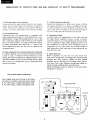
1. PARTS IDENTIFICATION
FRONT SIDE
lI~~~::::;:::::~::::~~~~~=POWERINDICATORLAMP
POWER SWITCH
REAR SIDE
r---------~-CONTRAST
H-HOLD
-i~~~I~11 :UUl:nUI:m~lmU...J,ill
SERIAL NO LABEL--II-I---!:r==,---tt---1-l
' - - - - - - - - - - - - - BRIGHTNESS
. V-HOLD
V-SIZE
Figure 1.
3
Z-1D05
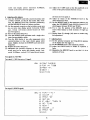
2. REMOVING MAIN PARTS COMPONENTS
-
r--
f'"o=
/If
(
lIt
I
11 I
......
CJ
r:=:J
c=J
~
11
i ••
Rear side of the-+--tI-<..
printed wire board.
,.ry~r
/
I
I
Figure 3.
Figure 2.
•
Remov,1 of the rear cover
Disconnect the AC cable.
2) Untighten two screws that secure the upper part
® and two other screws that secure the lower
part @ of the rear cover.
3) Remove the screw © then pull off rear cover.
4) Untighten the screw @.
1)
3. ADJUSTMENTS
• It needs a personal computer (Le. MZ-700) to carry out
adjustments.
• Even though everthing had been adjusted to their optimum points before the unit left the factory, it has to be
adjusted in the following manner whenever parts replacement is done or when an adjustment error should occur.
• Adjusting horizontal synchronization
(l) Set the personal computer so that the same letter
should be displayed on an entire screen area (on an
entire data display period: horizontal 36.088tLsec,
vertical 12.811msec), using such as alphabet letter
of "H" (see Test signal I).
(2) Adjust the H-HOLD knob so that the picture should
situate in a middle of the screen.
(3) Try to turn on and off power for a few times to see
that the picture is stayable.
• +B power supply circuit (It needs the voltmeter with
internal resistance of 20kohrns/V.)
(1) Ensure that the ac supply is above the rating below,
depending on power source rating.
228V for 240V set
209V for 220V set.
(2) Adjust the +B potentiometer so that there should
appear the de voltage of HOV between TP-91 and
ground.
NOTE-I) Supply of required HOV may not be obtained
when the source voltage is under the given rating,
but there would be no specific problem_
NOTE-2) Turning the +B potentiometer clockwise increases the +B Voltage. Watch the voltmete while adjusting so as to avoid too much voltage increase.
• Adjusting horizontal amplitude
(1) Set the personal computer so that the letter "H"
should be displayed on an entire screen area (on an
entire data display period: horizontal 36.088tLsec,
vertical 12.811msec) (see Test signal 1).
(2) Adjust the horizontal amplitude coil so that the amplitude on the center should become 245mm.
NOTE) Turning the horizontal amplitude coil clockwise
will make amplitude increased.
• Adjusting vertical amplitude
(1) Set the personal computer so that the letter "H"
should be displayed on an entire screen area (on an
4
entire data display period: horizontal 36.088tLsec,
vertical 12.81Imsec) (see Test signal I).
(2) Adjust the V-AMP knob so that the amplitude at th
center of the picture should become 183mm.
• Adjusting white balance
(1) Turn the SCREEN knob fully counterclockwise, each
of RED, GREEN, and BLUE bias knobs fully clockwise, the BRIGHT knob fully clockwise (maximum),
and the RED/BLUE knob to a midway position.
(2) Set the personal computer so that an entire screen area
(on an entire data display period: horizontal 36.088
tLsec, vertical 12.811msec) should become all white
(see Test signal 2).
(3) Pull out the service chip (VI).
(4) Turn the SCREEN knob clockwise until a single color
raster becomes slighdy visible.
(5) Turn the BIAS knobs of two other suppressed colors
counterclockwise so that raster should appear white
(gray). Slighdy decrease the SCREEN knob until raster
disappears.
(6) Replace the service chip (VI).
(7) Manipulate the personal computer so that an entire
screen area (on an entire data display period: horizontal 36.088tLsec, vertical 12.81lmsec) should remain
all white (see Test signal 2).
(8) Adjust by means of the RED/BLUE knob so tha
raster should turn white.
(9) Set the BRIGHT knob to the maximum position, thel
adjust the SUB-BRIGHT knob (R419) so that dc 5.6'
should appear between TP-402 and TP-403.
(10) Try to vary the position of the BRIGHT knob tl
ensure white balance at both extremes of bright anI
dark.
(11) Repeat Steps (3) through (10) above to attain comp
lete adjustment.
• Adjusting focus
(1) Set the personal computer and bring letters appearel
on the display (see Test signal 1).
(2) Set the BRIGHT knob to the maximum position.
(3) Adjust the FOCUS knob to obtain an optimum 0
focus.
(4) Manipulate the BRIGHT knob to see that it is in aJ
optimum of focus.
Test signal (ex: MZ-700)
Test signal I (1000 characters, H signal)
(EX.)
10
20
30
40
50
(EX.)
10
20
30
40
50
60
70
80
90
100
PRINT CHR$(6)
FOR 1= 1 T0999
PRINT "H";
NEXT I
GO TO 50
Test signal 2 (WHITE signal)
FOR 1=1 TO 7
COLOR ." I
PRINT "[Q)"
GET A$
IF A$=" "THEN 70
GO TO 40
NEXT I
COLOR ... 0
PRINT "[Q)"
END
5
Z-1D05
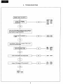
4. TROUBLESHOOTING
I
POWER NOT IN SUPPL V
I
1
Is there 130V between
positive pole of SCR701
and ground?
I
I
Ves
1
I
I
No
I
I
SW750
F701
F702
0701
: 0702
0703
:
0704
T702
T701
R701
C701
I
Insert zener diode (60V)-between the gate of SCR701
and the junction of F702 and 0705. (Connect to the
zenor diode at the gate of SCR701.l
1
Power circuit in operation
now?
l
I
Ves
1
L
J
L
I
No
L
J
Z0701 0705
Z0702 R704
I
Insert 500hms, 15W, resistor between TP91 and the
junction of F702 and 0705.
1
Horizontal synchronizing I
circuit in operation, now? I
I
I
Ves
I
I
I
I
I
I
I
I
1
~
.... -
1601
0601
0602
Z0601
R612
R613
R620
No
I
0604
R629
1701
R707
R711
R706
R709
C707
I
I
Is there 7.8V between 1701 and ground?
I
I
I
Is there 18V between 1701 and ground?
Ves
No
J
I
I
J_ .....
Ves
SCR701
R712
R705
C709
C710
6
J
I
No
I
I
:
•
MZ-1 DO
I
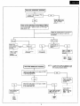
RASTER DOES NOT APPEAR
I
Is there 110V between TP91
and ground?
I
Yes
I
I
I
No
I
.~ ............1... _ ..
:
:
:
:
I
----
Power supply, horizontal synchronization, or protect
circuit
..... ----- -- ._----_ ... - _ ...
Check the de voltage level on the collector of 0851.
Under the normal condition the DC voltage could be
vary between 160 - 140Volt when turn the brightness control VR.
Check for contact failure in connectors
interfacing the video unit with the
computer.
I
I
Normal
I
I
Check the
video tube and
its peripheral
circuits .
.... _... J .........
T602 or C854
of the video
tube or
SCREEN VR
Not normal
(OK)
I
I
I
Signals on?
J
I
Yes
L
I
.-_ ..... --- ........ __ .... __ ._--.
_ .......1........
I nput circuit or
computer
....... -- .. _--_ ....... - ... -_ ..:
I nput circuit
or computer
....... -.. -_ .... _--
(No)
I
I
I
J
Is ther 6.4V on
the collector of
0402?
l
I
I
I
No
I
1
0401, or 0402, or
their peripheral
circuits
.. .... _.... 1.... _......
0401
0402
R413
Z0402
Z0401 :
._-- ...... __ ........... -..
I
PICTURE DOES NOT APPEAR J
1
NOTE: I n case pictu re does not appear on the
screen, try to turn the BRIGHT knob
fully clockwise before check.
-
Check the video signal on the base of Q452
using the oscilloscope.
Is the video signal on7
I
I
Yes
L
J
I
Yes
J
I
L
No
L
J
I
Check the video
input circuit and
its peripheral
circuits .
Check the video Signal on the base of 0851
using the oscilloscope.
Is the video signal on?
I
L
1
No
J
-1
Check 0452 through
Check 0402 and
its peripheral
circuits.
I
..... J.....
0851 and their peripheral ci rcuits.
_...1 ...
R850
0851
0401
Q402
Z0402
7
..... __ ... l. ..........
I nput cable, input socket,
1491, computer,
0451 -471,or
0451 - 471
____ -0-
•• _ • • • • • • • • • • •
iv1Z-1D05
SYNCHRONI ZA TION DISABLED
Horizontal or vertical
syncchronization not
enabled.
,---------- .. _.-----._._ ... _.... _-,
··:
1481
: R481
1601
R602
R483
...
R608:
C601 :
,--_ ....... _-_ .... - ... ----.-- ... _-,
,....-----1 HORIZONTAL SYNCHRONI·
If vertical synchroni·
zation is normal.
ZATION NOT ENABLED
Manipulate H·HOLD to see if a change is
met in the horizontal synchronizing fre·
quency.
•
Check appearance of sawteeth waveform
and synchronization signals on pin 14 of
1601.
1601 :
.:-_ ....
__ .. -..
1601
: R612
: R607
,....----1 VERTICAL SYNCHRONIZATION
If horizontal synchro.
nization is normal.
NOT ENABLED
A slight change may be met in the fre·
quency of vertical synchronization.
Vertical synchronization not possible to
adjust.
ii
1601
R502
C501:
C504:
1601
R510
R511
R512
R513
R514
C503
C505
/ VERTICAL SWEEP NOT ENABLED /IMPORTANT: Dec.rease brightness
wnng tha check to
avoid damaging the
video tube.
Ripple current signa
appears on the junction
of F702 and R703.
NOTE:
Send ripple current signal to pin 2 of 1601
via the serial connected resistor (1 kohms)
and capacitor (10",F).
I
_
.............. .1................
1601
R504
R505
R506
R507
R508
R509
R501
C503
R506
I
Does not sweep.
Raster is sweeped verti·
cally.
: 1601
.0501
: 0502
• DY601
.0504
. R505
R511
R512
R513
R514
R515
8
...
_-.-.
0502
0503
R503
R504
R507
R507
J
-------
R508
R516
R518
R519
R520
R524
C509
C510
C514
Continued on page13.
2
1
•
3
6
5
7
8
I.
9
11
12
6. PRINTED WIRING BOAD ASSEMBLIES
A
A
,
N.
••• ••
•
•
•
~
o
o
••o
o
1
T
• •
c
c
o
•o
~
..
•
•
0
•
0
•
D40 ~
..
I '"
•
, J
P.W.B-B CRT Soeht BNrd (Wiring Side)
I
'l~
4 19
S!J8. 6'l I ~' t3 1j(l$
( e ....
11606
R62"
- ,
4~13
" 01
H ,lI!]ll
I
1162]
11622
•
. ...
N
:il
"
E
C'09~Y
~ 1Q'
••
ff
,
•
N
•
~
N
. '0'
00(1)
e
-
0
u
u
~roo
I
E
I
140V
••
j
1
,
I.
•
•
••
,
o
N
•
060 .
•
•
"."
ID]. l
I
•
N
••
11630
Po_ SupplV P.W.B.
1161 2;,.-_ _" ,
•
'.
,~,
G
•••
N
•u
, , ,
N
•
,
,
••
u
H -CEN1 ER
U'
""
11626
,
o
(
N
•
11:
.,-.
•
~ T
u
I
11607 ~
H-HOLD
H
,
IF IDIOTAI
•
3
5
G
,
.1
rn
,~
1
"""0'
ROO"
tI
u
I
III
RU t
ZOGO!
,
o
o
o
"
1 6 02
6
7
H
8
I.
9
12
11
•
11
12
MZ-1005
I
SPECIFIED COlOR DOES NOT APPEAR.
I
Raster in red or cyan
Raster in green or
magenta
Raster in blue or yellow
Check the red video circuit
at 1491,0451, 0452, and
0851.
Check the green video
circuit at.0462, 0461
and 0852.
Check the blue video
circuit at 0472, 0471,
and 0853.
. ......... _.. _......... --------..
. ............... ............. -.-...
··._o •....•.••••.•.•. _____ ..••...•
~
1491
0451
0851
0451
R856
R863
R866
R880
C850
C856
0452
1491
0462
0461
0852
0461
R864
R867
R881
C851
C857
1491
0472
0471
0853
R858
R865
R868
R882
0471
C852
C855
.......... __ . __ ..... _----_ .........'
Continued from page8.
13
MZ-1D05
CHASSIS LAYOUT
_ _ _ _ _- 7
_0
CAT
370MAB22 .
H.V
CATPWB
~3NVEAGENCE
RITY MAGNET)~~~?
CAT PWB
~
B BIAS
B DRIVE
G BIAS
R DRIVE
A BIAS
_ ....._.J..:.LSEAVICE TIP
H.VCA BLOCK
H.V
(2)
•
L
< 1481
INPUT CIRCUIT
<
1491
MAIN PWB
~
':~:
8
e
~
~CD
11 +S.
R707A DJ
("OV)
VERTICAL OUTPUT
R419
IKl IiI
L"'J
POWER
"'''''' OUTPUT
•
CG_~USPAC~
FUSE
___- 1701
EGULATO
F702 R
____
TI.6A
-
--~-,~
~
n
'
V::':
"'"
CIRCUIT
~o [-j ,~NE
, ...
V Lt
R H.V
0
t:',
_
~
;, :::--~.'C H~
'/~;;____
C:H~O==60=2===§-J --; ~V.P.~~~~ION
SIDE
PINCUSHION
_
. OUTPUT
2
0H. SIZE
3
. ---------
5~D (.~
T60I
.F.B~
_~~. ' . ii}.
"."
H. DRIVE
!I _ I
'SCREEN
R!114
~
E@lH
.
POSITION
i
':
.
....
')
I.
V. SYNC R507 R&07
.v. SI~E SYNC."420
"415
BRIGHTNESS CONTRAST
14
T
701
P. T.
MZ-1D05
NOTES ON WIRING DIAGRAM
2. Resistor and capacitor rating description
I Resistor I- Capacity: No mark: ohms K: Kohms
M: Mohms
No mark: ±10% J: ±5%
- Error
~_ _~- Rated power: No mark or: 1/4W
No mark or p.: p.F
Capacitorl- Capacity:
P:pF
- Rated voltage: No mark: 50V
*There may be a slight difference depending on the serial
number, because this wiring diagram is the basic wiring
diagram.
Since the parts component noted with a " t, " mark is critical for safety performance, it has to be replaced with the
genuine parts for safety's sake, as well as maintaining proper performance of the unit.
I
[Type]
1. Voltage values and waveforms indicated in the wiring
diagram are the values that measured with the personal
computer (MZ-700) in connection and with the video
input signal of OV (screen not working), under the
given rating.
NOTE-I: Voltage value is the value measured by the
20kohms/V voltmeter.
NOTE-2: (H) and (V) in waveform description represent
repeat frequency.
(H): 15.61Hz, (V): 50.0Hz
Capacitor
Resistor
No mark
No mark
Carbon film
Ceramic
C
Solid
ML
Mylar
S
Metal oxide film
PF
Polypropylene film
N
Metal film
W
Cement
TA
Tantalum
T
Special
ST
Styrol
Film
3. Test point noted in parenthesis has no pin.
8. LEAD WIRE SHAPING AND WIRE THREADING METHOD
~
To LED
,....---" ~ -UL Tube
Coating earth lead ~_--%it-ft"-~
UL Tube
WH
C.V. Sheet
15
9. PACKING OF THE SET
• Knob Positions
Acc_ri.
Poly. bag
(SSAKAOOO3GEZZ)
,--------------------------,
~
p
L -______________________________
a
'--)i;J
I
T
Instruction Book
(TINSZ7011TAZZ)
~
POWER . • • . . . • . , OFF
H-CENTER . . . • . • • BEST
V-HOLD. . . • .• NORMAL
BRIGHT . • . • . • • • . BEST
,
,,,
Oast cover
(SPAKP6416TAZZ)
I
I
I
AC cord
..,~
~
~..,
,"
~
Prlnt~ material in the
beg I. contained.
Cushion
(SP AKA6416T AZZ)
Carton
Europe Except UK (SPAKC7011TAZZ)
UK only (SPAKC7010TAZZ)
Serial number card
(TLABKOO01 TAZZ)
t'1
Top and bottom are stapl~.
16
MZ-1005
PARTS LIST
[I] Tube, IC
NO.
PARTS CODE
1
2
3
4
VB370MAB22/1E
RH-iX0065CEZZ
RH
iX0137CEZZ
VHiHD7406//-1
PART
RANK
B
B
B
B
Picture tube
IC(H AND V)
IC1SCR Power}
IC
PRICE NEW
RANK MARK
AM
AB
AC
AB
AG
AF
AD
AM
PART
RANK
B
B
B
B
B
B
B
B
Thyristor
Transistor
Transistor
Transistor
Transistor
Transistor
Transistor(H
Transistor
PRICE NEW
RANK MARK
AA
AB
AB
AA
AC
AF
AD
AB
AB
AB
AB
AD
AB
AD
PART
RANK
B
B
B
B
B
B
B
B
B
B
B
B
B
B
Diode
Diode
Diode
Diode
Diode
Diode
Diode
Zener diode
Zener diode
Zener diode
Zener diode
Zener diode
Zener diode
Photo transistor
PRICE NEW
RANK MARK
**
AM
AG
AF
DESCRIPTION
[1601 ]
[1701 ]
[1481/491]
[2J Transistors
PARTS CODE
NO.
&.
1
2
3
4
5
6
7
8
VHSS6192FLBIE
VS2SAI015Y/IE
VS2SA854-Q/1E
V S 2 S C 1 8 1 5 Y W- 1
VS2SC1826GL2E
V S 2 SC 2 0 6 8 L B 1 E
VS2SC2482//-1
VS2SD869 / / 1 E
DESCRIPTION
[SCR701 ]
[0401451461471]
[0402]
[0452462472]
[0501,0502]
[0851 852 853J
[0601]
[0602]
Drive)
~ Diodes and LED'S
NO.
1
2
3
4
5
6
7
8
9
10
11
12
13
14
PARTS CODE
RH DX0033TAZZ
RH DX0038CEZZ
RH DXOO46CEZZ
RH DX0048CEZZ
RH D X'O 0 8 6 T A Z Z
RH DXOI00CEZZ
RH-DX0101CEZZ
RH-EX0041TAZZ
RH-EX0043CEZZ
RH-EX0047CEZZ
RH-EX0049CEZZ
RH-EX0061CEZZ
RH EX0069CEZZ
RH PX0034CEZZ
DESCRIPTION
[D451 461 471]
[D701-7041S1887]
[D401]
[D402-405]
[D603 605 504]
[D602 BOOST]
[D604 FR-1]
[ZD402]
[ZD701702]
[ZD602]
[ZD481]
[ZD401 ]
[ZD601]
[D708]
Packaged circuits
DESCRIPTION
PARTS CODE
Block resistor
NO.
1
2
3
4
5
6
7
8
9
10
11
12
PARTS CODE
RCiLF0068CEZZ
RCiLG0135CEZZ
RCiLH1347CEZZ
RCiLZ0155TAZZ
RCiLZ0213CEZZ
RTRNC0028CEZZ
RTRNF1242CEZZ
RTRNP0363TAZZ
RTRNP0364TAZZ
RTRNQ0044CEZZ
RTRNZ0059CEZZ
VP-LKI20KOOOO
[PR701 ]
PRICE NEW
RANK MARK
AH
AM
N
BG
N
AN
AG
AK
BG
BL
BL
AL
AG
AB
PART
DESCRIPTION
RANK
Coil
C
Degaussing coil
C
Deflection yoke
B
COil(H Size)
C
Coil
C
Choke transformer( + B Choke)
B
H VOLT Transformer
B
Power transformer(Europe except U.K)
B
Power transforrner(U.K. only)
B
Pin-Cushion trans(Side-Pin}
B
Transformer(Drive}
B
Peakinlr coil
C
PRICE NEW
RANK MARK
AD
AD
AC
AC
AE
AD
AD
AC
AC
PART
RANK
B
B
B
B
B
B
B
B
B
Variable
Variable
Variable
Variable
Variable
Variable
Variable
Variable
Variable
PRICE
RANK
AH
AC
AA
AA
AA
AA
AC
AC
PART
RANK
C
C
C
C
C
C
C
C
Capacitor
Capacitor
Capacitor (50WV l~F)
Cajlacitor(50WV 220pF)
Capacitor (50WV 180pF)
Cajlacitor (50WV 39pF)
Cajlacitor (6.3WV 470uF)
Capacitor (16WV 10uF)
[L702]
[ADG L701]
[DY 601]
[L603]
[L604]
[T702 +B]
[T602]
[T701]
[T701 ]
[T603]
[T601]
[L601]
[ID Controls
NO.
1
2
3
4
5
6
7
8
9
PARTS CODE
RVR B4224CEZZ
RVR B4225CEZZ
RVR-B4454CEZZ
RVR-B4462CEZZ
RVR-B7076TAZZ
RVR-B7082TAZZ
RVR-B7083TAZZ
RVR-M7046TAZZ
RVR-M7242TAZZ
DESCRIPTION
resistor(Drive)
resistor
resistor(V - Line)
resistor(SUB BRIGHT)
resistor
resistor
resistor
resistor(+B ADJ}
resistor(H CENT)
[R856858]
[R863-865]
[R526 200B]
[R419]
[R415420]
[R514607]
[R507]
[R707]
[R619]
[1J Capacitors
NO.
1
2
3
4
5
6
7
8
PARTS CODE
RC F ZOO 0 4 C E Z Z
RC-KZ004JCEZZ
VCCSPAIH6150J
VCCSPAIH0221J
VCCSPAIH6181K
VCCSPAIH6390K
VCEAAUOJW477M
VCEAAAICWI06M
NEW
MARK
N
N
N
N
DESCRIPTION
17
[C701]
[C703 704 618]
[C451 461 471]
[C855-857]
[C502]
[C511 ]
[C513]
[C602607]
Z-1005
rn Capacitors
NO.
\
\
\
"
PARTS CODE
9 VCEAAA1CW107M
10 VCEAAA1CW226M
11 VCEAAA1CW227M
12 VCEAAA1FW106M
13 VCEAAU1EW107M
14 VCEAAA1EW337M
15 VCEAAA1EW476M
16 VCEAAU1EW477M
17 VCEAAA1HW105M
18 VCEAAA1HW106M
19 VCEAAA1HW337M
20 VCEAAU1HW475M
21 VCEAAA1HW476M
22 VCEAAH2CW107Y
23 VCEAAH2EW226Y
24 VCEAAUOJW477M
25 VCEACA1CC336K
26 VCEHAQ2CBA31Y
27 VCFPPD2DB474J
28 VCFPPD3CA822J
29 VCFPPD3CB392J
30 VCKYATIEXI03N
31 VCKYATIHB151K
32 VCKYPA2HB102K
33 VCKYPA2HB472K
34 VCKYPB2HB103K
35 VCKZPA1HB102K
36 VCKZPAIHB103K
37 VCKZPAlHB15lK
38 VCKZPAlHB22lK
39 VCKZPA1HB472K
40 VCKZPA1HF103Z
41 VCKZPA1HF223Z
42 VCQPSA2AA272G
43 VCQPSB2DA473K
44 VCQYSH1HM104K
45 VCQYSH1HM183K
46 VCQYSHIHM222K
47 VCQYSH1HM273K
48 VCQYSHIHM563K
49 VCQYSH1HM682K
50 VCSATA1VE225K
PRICE NEW
RANK MARK
AB
N
AB
AC
N
AB
AB
AD
AB
N
AD
AB
AB
AD
AB
N
AC
AF
AE
AC
AD
N
AN
AF
AE
N
AD
N
AA
AA
N
AA
AB
AC
AA
N
AA
N
N
AA
AC
AA
N
AA
N
AA
AD
AB
N
AC
N
AB
AA
N
AB
N
N
AB
N
AA
N
AC
PART
RANK
C
C
C
C
C
C
C
C
C
C
C
C
C
C
C
C
C
C
C
C
C
C
C
C
C
C
C
C
C
C
C
C
C
C
C
C
C
C
C
C
C
C
Capacitor (lOOuF 16V)
Capacitor (l6WV 22uF)
Capacitor (220uF 16V)
Capacitor (25WV 10uF)
Capacitor125WV 100uF)
Capacitor (25WV 330u'F)
Capacitor(25WV 47pF)
Capacitor(25WV 470pF)
Capacitor(50WV IpF)
Capacitor (50WV 10"F)
Capacitor 50WV 330jlF)
Capacitor 50WV 4. 7Jif~
Capacitor 50WV 47"F)
Capacitor 160WV 100uF)
Capacitor 250WV 22uF)
Capacitor 6.3WV 470uF)
Capacitor 16WV 33"F)
Capacitor (l60WV)
Capacitor (200WV 0.47pF)
Capacitor (l600WV 8200pF)
Capacitor (1600WV 3900pF)
Capacitor (25WV O.OlpF)
Capacitor (50WV 150pF)
Capacitor (500WV 1000pF)
Capacitor(500WV 4700pF)
Capacitor (500WV 0.010pF)
Capacitor (50WV 1000pF)
Capacitor(50WV 0.010jlF)
Ca pacitor (50WV l50pFJ
Capacitor 220pF 50V)
Capacitor 50WV 4700pF)
Capacitor 50WV O.OluF)
Capacitor 50WV 0.022pF)
Capacitor 100WV 2700pF)
Capacitor 200WV 0.047uF)
Capacitor 50WV 0.10pF)
Capacitor (50WV 0.018pF)
Capacitor (50WV 2200pF)
Capacitor (50WV 0.027pF)
Caoacitor (50WV 0.056J.LF)
Capacitor (50WV 6800pF)
Capacitor (35WV 2.2"F)
PRICE
RANK
AB
AA
AA
AA
AA
AA
AA
AA
AA
AA
AA
AA
AA
AA
AA
AA
AA
AA
AA
AA
AA
AA
AA
AA
AA
AA
AA
AA
AA
AA
AA
AA
AA
AA
PART
RANK
C
C
A
C
C
C
C
C
C
C
C
C
C
C
C
C
C
C
C
C
C
C
C
C
C
C
C
C
C
C
C
C
C
C
Resistor (lOO)
Resistor (l/2W 2.7KO +10%)
Resistor (1/2W 4.7KO ±10%)
Resistor (1/2W 470KO ±10%)
Resistor (1/8W l.8KO ±5%)
Resistor (1/4W 1.00 ±5%)
Resistor (1/4W 1000 ±5%)
Resistor (1/4W 1.0KO ±5%)
Resistor {lOKO 1/4W +5%)
Resistor O/4W 1200 +5%)
Resistor 1/4W 1.2KO +5%)
Resistor 1/4W 12KO +5%)
Resistor 1/4W 1500 +5%~
Resistor l.5KO 1/4W +5%)
Resistor (1/4W 15KO ±5%:
Resistor (l/4W 1.8KO ±5%)
Resistor (1/4W 18KO +5%)
Resistor{I/4W 2.2KO +5%)
Resistor 1/4W 220KO +5%)
Resistor 1/4W 2700 +5%)
Resistor 1/4W 2.7KO +5%)
Resistor 1/4W 3300 +5%)
Resistor 1/4W 3.3KO +5%)
Resistor 1/4W 33KO +5%:
Resistor 1/4W 3900 +5%:
Resistor 1/4W 3.9KO +5%)
Resistor (l/4W 470 +5%)
Resistor (1/4W 4700 +5%)
Resistor (l/4W 4.7Kn +5%)
Resistor(1/4W 47KO +5%)
Resistor (1/4W 560 +5%)
Resistor (5600 1!4W +5%)
Resistor (1/4W 5.6KO +5%)
Resistor O/4W 56KO +5%)
DESCRIPTION
[C505 608 626]
[C401]
[C404481]
[C508]
[C405]
[C621 ]
[C406]
[C509]
[C504603]
[C403]
[C510]
[C615]
[C708]
[C707/619]
[C853]
[C515]
[C507]
[C706(A),(B)]
[C622]
[C616]
[C61?]
[C402]
[C850]
[C610]
[C710]
[C705/623]
[C609/614]
[C71 1/712/482/61 1]
[C85l C852]
[C49l-493]
[C506]
[C40?]
[C714]
[C604]
[C709]
LC620J
[C60l]
[C606]
[C6l3]
[C501 612]
[C605]
[C5035l4]
[ID Resisto rs
NO.
1
2
3
4
5
6
7
8
9
10
11
12
13
14
15
16
17
18
19
20
21
22
23
24
25
26
27
28
29
30
31
32
33
34
PARTS CODE
RR-XZOO19GEZZ
VRC-MA2HG272K
VRC-MA2HG472K
VRC-MA2HG474K
VRD-RA2BE182J
VRD-RA2EE1ROJ
VRD-RA2EE101J
VRD R A 2 EEl 0 2 J
VRD R A 2 EEl 0 3 J
VRD-RA2EE121J
VRD R A 2 EEl 2 2 J
VRD-RA2EE123J
VRD-RA2EE151J
VRD-RA2EE152J
VRD-RA2EE153J
VRD-RA2EE182J
VRD-RA2EE183J
VRD-RA2EE222J
VRD-RA2EE224J
VRD R A 2 E E 2 7 1 J
VRD R A 2 E E 2 7 2 J
VRD-RA2EE331J
VRD-RA2EE332J
VRD-RA2EE333J
VRD-RA2EE391J
VRD-RA2EE392J
VRD-RA2EE470J
VRD R A 2 E E 4 7 1 J
VRD R A 2 E E 4 7 2 J
VRD R A 2 E E 4 7 3 J
VRD R A 2 E E 5 6 0 J
VRD R A 2 E E 5 6 1 J
VRD-RA2EE562J
VRD-RA2EE563J
NEW
MARK
N
N
N
N
N
N
N
N
N
N
N
N
N
N
N
N
N
N
DESCRIPTION
18
[R628]
[R880-882]
[R6ll]
[R883]
[R752]
[R629620]
[R624625]
[R408/451/46l/471]
[R405 407 622 505]
[R4l0]
[R409 452 462 472]
[R511 606403]
[R853]
[R411]
[R603 710 632]
[R418]
[R713]
[R502]
[R869]
[R491-494]
[R504709]
[R456]
[R513 516 454 464]
[R703]
[R402 503610]
[R623]
[R851852]
[R4l3 453,436 473]
[R509602,626]
[R5l2]
[R712]
[R71 1,481 483]
[R404]
[R706]
MZ-1D
[8l Resistors
..----.------------- . .
~
PRICE I NEW ! PART
I
PARTS CODE
RA~lA~f
-35 v R D - RA2EE682J .- ~
_
_.Lu Resistor (1I4W
-36 VRO- R A 2EE6-S3J--- _~A_N_._ _C__ Resistor (1/4W
37 VRD-R A 2 Tr684T- ~!- _of'!
-.f- t Resistor (1/4W
--38 V R D - R A 2 E E 8 2 0 J .I
-39 VR"-O-R ';'-2 E E8Zrj-
NO.
DES CRI P T ION
--- --_._- ----- .._-
6.8Kn!ff!!l._________ n________ ~ _______
68KO :!:5%)
. ______
680Kil +5%)
_____________ .. ______ ...
0
-~ ~ -N-+-~· ::~:~~~_H~:~ ~~go:!:;~9h--
_ _ _ _ _ _ _ _ . _ _ _. . _ _ _ . _
------.---------------------
[R515]
[R605]
[R608]
~:~~~ ~~i~
[R604]
~O-+_"'B..Q=~!...U..1..._J__.A A I _ _ -1_J2..._.t.~e.slstorill~'!'{_8 2KO i:5..%2_~ __ ____________
---__41.' V R D- B~£:..i..S. ?..!_J_~-t-_. __ j-_Q.._ I Resistor (1/4W 8J.QK_!L:!:5%2 ______.________
[R708]
----_._- ._- -[R524]
-~nB..Q-=-B..6.2 H D.l~Q.J__ A A i N I .. C I Resistor (1/2W 1 00 :!:5%2
----_._- -- -.
[R530]
~ VRD-RA2!i~j-LL-!-W._t-f'!..-l
C
ReslstorQ/2W4700:!:5%)
_____________ ... ___ ._.
44 V R D- RA 2 H D 6 R 8 J
A AN'
C
ReSistor (l/2W 6.80 :!:5%2
[R615--618]
[R521 ]
~i. V ~~1Ji D_ 1.Jl2.L .L_~_L+ ~
L ~~SISI£.r..liL2~ 1 OKO :!: 5%1. ______________ .
[R508]
A 2!!.Q)
C
ReSistor (3 9n 1/2W :!:5%)
____ ._________ ..____._____._ .
47 VR...Q.=-RA2HD~L
.f.~
_N_-l
C _llislstor(I/2W390n:!:5%)
_______. _____________ .___
[R519]
~8 rv-R-D-R !\_~I:t.Q 2~LJ.. __ f ~.f.- f--_fIl __ L_C
ReSistor (l/2W 220n :!:5%) _____
[R528]
- ----------- "-49-VRD-RA2HD5R6J
AA
NI
C
I Resistor (1/2W 5.60 +5%)
[R518]
[R529]
- . - - - --------_.
-~Q _~D - R !\-~..I:f...Q.l....Q..1-4--- ~ __ f--N I C ! Resistor (1/2W 1000 +5%)
I Resistor (l/4W 150n +5%)
fI A .
N
C
[R855857]
-_.
------------ --~~ VRD-RU2EE151J
R D --ifU2E E_i. 7
AA I
Resistor (1/4W 470 :!:5%)
C
52
[R850]
- - ' - ._- --------------_.._.-AAl
i
j
C
Resistor(I/4W 8200 :!:5%)
53 VRD-RU2EE821J
[R862]
AB
Resistor (1 W 0.470 :!: 5%)
54 VRN-RU3AAR47J
C
[R627]
N
AB
C
Resistor (1 W 3.90 :!: 5%2
5!J VRN R U 3 A A 3 R 9 J
[R527]
--------"
AA
C
ReSistor (1/2W 1500 :!:5%)
56 VRS-PU2HB15 1 J
[R704]
---N
AA
Resistor (1/2W 820 :!:5%2
C
[R506]
~ 57 VRS-PU2HB820J
._-C
Resistor (1 W 2700 :!: 5%}
58 V R S-P U 3 AB 27 1 J__ AA
[R401]
AA
Resistor Cl W 3900 + 5%)
C
59 VRS-PU3AB391J
[R520]
AA
Resistor (l W 3.9KO :!:5%)
60 VRS P U 3 A B 3 9 2 J
C
[R406]
_.AA
C
Resistor11 W 5.6KO + 5%)
61 VRS-PU3AB562J
[R866-868]
AA
Resistor 1W 8200 +5%)
C
62 VRS-PU3AB82fJ
[R631]
AA
C
Resistor 2W 1000 +5%)
63 VRS-PU3DB10 1 J
[R484]
~
AA
C
Resistor 2W 1.2KO :!:5%)
64 VRS-PU3DB122J
[R613]
AB
Resistor 3.9KO 2W :!:5%)
C
65 VRS-PU3DB392J
[R523]
AB
Resistor (2W 3300 :!: 5%)
VRS-PU3DB331J
C
[R705]
~~
AB
Resistor (2W 8.2KO :!:5%)
C
\
67 VRS-PU3DB822J
[R612]
AA
C
Resistor (1 W 5600 :!:5%)
68 VRS-PV3AB561J
[R630]
AC
C
Resistor (5W 1.80 :!: 10%)
69 VRW KV3HC1R8K
[R701]
N
AA
Resistor{1/2W 1.5KO :!:5%)
70 V R D--R A 2 H D 1 5 2 J
C
[R522]
---~-
+
_.:I6~_=-R
.0_
_
_ _
• _ _ _ _ _ _ _ _
_L
~~-.L-E~-+---- l _
---.---------~----
nO
ry-
•
-o-t=
_
--~.---.
-----~-
.---------~-----------------
.-----~----
~ Miscellaneous parts
NO.
1
2
3
4
5
6
7
8
9
10
11
12
13
14
15
16
17
18
19
20
21
22
23
24
25
26
27
28
29
30
PARTS CODE
PMAGF3003CEZZ
PRDAF0221TAZZ
PRDAF0222TAFW
PRDAR1126CEFW
PRDAR5018CEZZ
PSlDM0384TAZZ
PZETVOOO7TAZZ
PZETV0109TAZZ
QACCBOO11TAZZ
QACCZOO26TAZZ
QCNW-0348TAZZ
QFS-C1621TAZZ
QFSHD1002CEZZ
QPlGN0109TAZZ
QPlGN0207CEZZ
QPlGN0213GEZZ
QPlGN0304CEZZ
QPlGN0403CEZZ
QPlGN0408CEZL:
QPlGN0505CEZZ
QSOCAOO16TAZZ
QSOCN0102CEZZ
QSOCN0210GEZZ
Q SQC N 0 3 0 2 C E Z Z
QSOCV1425CEZZ
QSPGCOO10CEZZ
QSPGC0011CEZZ
QSPGHOO13CEZZ
QSW P0047TAZZ
QTANZOO13TAZZ
PRICE
RANK
AK
AG
AG
AE
AB
AA
AA
AF
BB
AY
BB
AE
AA
AC
AA
AA
AB
AB
AB
AB
AK
AA
AB
AA
AH
AB
AC
AF
AN
AG
NEW
MARK
N
A
C
C
C
C
C
C
C
C
C
C
C
C
C
C
C
C
C
C
PRICE
RANK
AC
AE
AB
AE
AS
AB
NEW
MARK
N
N
N
N
N
N
PART
RANK
C
C
C
C
C
C
N
N
N
N
N
N
N
N
N
N
N
PART
RANK
C
C
C
C
C
C
C
C
D
D
DESCRIPTION
Magnet
Heat sink
Heat sink
Heat sink
Heat sink
Shield
Insulator
Insulator
AC cord(U.K. only)
AC cord(EUROPE except U.K.)
Connecting cord
Fuse (1.6A)
Fuse holder
Plug (3pin SW)
Plug (2P)
Plug (lED YO)
Plug (3pin AC YO)
Plug (4P-PlG)
Plug (4pin PT)
Plug (DY yD)
Socket AC-INlET
Socket
Socket (2pin-lED)
Socket
Socket
Spark gap
Spark gap
Spark gap
Push switch
Terminal
,
[F701]
[F702-YO]
[SW750]
[Q) Mechanical parts
NO.
1
2
3
4
5
6
PARTS CODE
lANGB0111CEFD
lANGK0210CEZZ
lANGQn70CEzZ
lANGR9038CEZZ
lANGR9039CEZZ
lANGT9159CEZZ
DESCRIPTION
Fixing
Fixing
Fixing
Fixing
Fixing
Fixing
metal
metal
metal
metal
metal
metal
19
[Q501 502 YO]
[Q501 502 YO]
[0602 H-OUT-YO]
[SCR YO]
-
Z-1065
[IQ] Mechanical parts
NO.
PARTS CODE
7 lANGT9344CEZZ
8 MSPRTOO01CEFJ
9 PCAPH1010CEZZ
10 PCAPH8013CEZZ
PRICE NEW PART
RANK MARK RANK
AH
N
Fixing metal
C
AA
N
Spring
C
AF
C
Cap
Cap
AC
N
C
DESCRIPTION
[ll] Screws,Nuts,Washers and Wire holder
NO.
1
2
3
4
5
6
7
8
9
10
11
12
13
14
15
16
17
18
19
20
21
22
23
24
25
26
27
28
29
30
31
32
33
36
37
38
39
40
41
42
PARTS CODE
l Hl 0 F 1 0 1 6 C EZ Z
lHlOW1013TAZZ
lHlOW1033CEOO
lHlOW1037CEZZ
lHlOW1046CEZZ
lHlOW9003TAZZ
lX-BZ3086CEFO
lX-CZ3002CEFO
lX-NZ0023TAFO
lX-NZ3014CEFN
lX-NZ3043CEFO
lX-NZ3062CEZZ
PS P AG 0001 C EO 0
PSPAG0023CEZZ
XCASC40P25000
XCAS030P08000
XCAS030P10000
XCAS030P12000
XCAS040P10000
XTAS030P10000
XTAS040P12000
XT A S 0 4 0 P 1 6 0 0 0
XTAS040P25000
XTBS050P20000
XUASC40P20000
XWHS045-12150
XWSPN30 o 6 0 0 0
GNETC0037CEZZ
PCliC1003CEZZ
QlUGP0102CEFW
QlUGP0104TAFW
QlUGP0105CEFW
QLUGZ0105CEZZ
QTiPFOO01CEFM
QTiPMOO05CEZZ
QTiPMOO07CEZZ
QTiPMOO08CEZZ
QTiPMOOIOGEZZ
RRET-0053CEZZ
SPAKA6416TAZZ
PRICE NEW PART
RANK MARK RANK
AB
N
Holder
C
AB
N
C
Holder
AA
N
C
Holder
AA
N
C
Holder
AA
N
Holder
C
AA
C
Holder CSdin cable YO)
AA
N
C
Screw
AA
N
C
Screw
AA
N
C
Nut
AA
N
C
Nut
AA
N
C
Nut
AA
N
C
Nut
AA
N
Spacer
C
Spacer
AC
C
AA
Screw
C
AA
Screw
C
AA
N
C
Screw
AA
N
C
Screw
AA
N
C
Screw
AA
N
C
Screw
AA
N
Screw
C
AA
Screw
C
AA
N
Screw
C
AA
N
C
Screw
AA
C
Screw
AA
N
C
Washer
AA
N
C
WasherCAC Inlet)
AD
N
C
Net
AA
N
Clip
C
AA
lug
C
AA
lug
N
C
AA
N
lug
C
AA
N
Lug
C
Tip
AA
N
C
Tip
AA
N
C
Tip
AA
N
C
Tip
AA
N
C
Tip
AB
N
C
BG
B
Rectifier unit
AM
0
Packing add.
DESCRIPTION
[TP91/701/402/32]
[2J Ca bi net pa rts
NO.
1
2
3
4
5
6
7
8
9
10
11
12
13
14
15
16
17
PARTS CODE
GCABA1390CESA
GCABB1343CESF
G C_O V H 7 0 4 3 TA Z Z
HBOGBI002CESA
HBOGCOO16TASA
HOECC0039CESB
JBTN-1104CEKB
TCAUA0057TAZZ
TCAUS0386TAZZ
TCAUS0417TAZZ
TlABKOOOITAZZ
TlABM0243TAZZ
TlABM0997TAZZ
TlABM0998TAZZ
TlABN0022TAZZ
TlABS0039TAZZ
TlABS0041TAZZ
PRICE NEW PART
RANK MARK RANK
BD
N
0
Cabinet
BH
0
N
Cabinet
AC
N
0
Cover
0
Badge(SHARP badge)
AD
AC
0
Badge
AD
Decoration plate
0
AE
Button
0
AD
N
0
Caution card
0
AB
Caution card
AC
N
0
Caution card
AA
Label
0
0
Label
AC
N
0
LabeICU.K. only)
AC
N
Label(EUROPE except U.K.)
AC
N
0
Label
0
AA
N
0
Label
AB
AB
0
label
N
DESCRIPTION
[U The others parts
NO.
1
2
3
4
5
PARTS CODE
SPAKC7011TAZZ
SPAKC7010TAZZ
SPAKP6416TAZZ
SSAKAOO03GEZZ
TiNSZ7011TAZZ
PRICE NEW PART
DESCRIPTION
RANK MARK RANK
AT
N
0
Packing case(EUROPE except U.K.)
AT
Packing caseCU.K. only)
N
0
Wrapping paper
AE
0
Vinyl bag
AA
0
N
0
Instruction book
SHARP CORPORATION
Industrial I nstru ment Group
Reliability & Quality Control Dept.
Yamatokoriyama, Nara 639-11, Japan
July 1983
Printed in Japan @