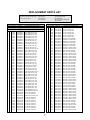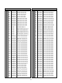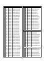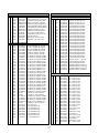
1
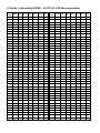
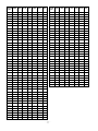
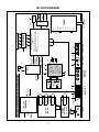
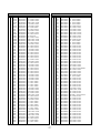
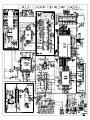
website:http://biz.LGservice.com
e-mail:http://www.LGEservice.com/techsup.html
LCD TV
SERVICE MANUAL
CHASSIS : ML-024H
MODEL : RZ-14LA60
CAUTION
BEFORE SERVICING THE CHASSIS,
READ THE SAFETY PRECAUTIONS IN THIS MANUAL.
CONTENTS
CONTENTS .............................................................................................. 2
PRODUCT SAFETY ..................................................................................3
DESCRIPTION OF CONTROLS .............................................................. 4
SPECIFICATION ........................................................................................7
ADJUSTMENT INSTRUCTION .................................................................9
TROUBLE SHOOTING ............................................................................14
BLOCK DIAGRAM...................................................................................15
EXPLODED VIEW .................................................................................. 16
EXPLODED VIEW PARTS LIST ..............................................................17
REPLACEMENT PARTS LIST ............................................................... 18
SVC. SHEET ...............................................................................................
SAFETY PRECAUTIONS
IMPORTANT SAFETY NOTICE
Many electrical and mechanical parts in this chassis have special safety-related characteristics. These parts are identified by
in the
Schematic Diagram and Replacement Parts List.
It is essential that these special safety parts should be replaced with the same components as recommended in this manual to prevent
X-RADIATION, Shock, Fire, or other Hazards.
Do not modify the original design without permission of manufacturer.
General Guidance
Before returning the receiver to the customer,
An isolation Transformer should always be used during the
servicing of a receiver whose chassis is not isolated from the AC
power line. Use a transformer of adequate power rating as this
protects the technician from accidents resulting in personal injury
from electrical shocks.
always perform an AC leakage current check on the exposed
metallic parts of the cabinet, such as antennas, terminals, etc., to
be sure the set is safe to operate without damage of electrical
shock.
Leakage Current Cold Check(Antenna Cold Check)
It will also protect the receiver and it's components from being
damaged by accidental shorts of the circuitry that may be
inadvertently introduced during the service operation.
If any fuse (or Fusible Resistor) in this TV receiver is blown,
replace it with the specified.
When replacing a high wattage resistor (Oxide Metal Film Resistor,
over 1W), keep the resistor 10mm away from PCB.
Keep wires away from high voltage or high temperature parts.
With the instrument AC plug removed from AC source, connect an
electrical jumper across the two AC plug prongs. Place the AC
switch in the on position, connect one lead of ohm-meter to the AC
plug prongs tied together and touch other ohm-meter lead in turn to
each exposed metallic parts such as antenna terminals, phone
jacks, etc.
If the exposed metallic part has a return path to the chassis, the
measured resistance should be between 1MΩ and 5.2MΩ.
When the exposed metal has no return path to the chassis the
reading must be infinite.
An other abnormality exists that must be corrected before the
receiver is returned to the customer.
Leakage Current Hot Check (See below Figure)
X-RAY Radiation
Warning:
The source of X-RAY RADIATION in this TV receiver is the High
Voltage Section and the LCD PANEL.
For continued X-RAY RADIATION protection, the replacement
panel must be the same type panel as specified in the
Replacement Parts List.
To determine the presence of high voltage, use an accurate high
impedance HV meter.
Adjust brightness, color, contrast controls to minimum.
Measure the high voltage.
The meter reading should indicate
23.5
1.5KV: 19-21 inch,
1.5KV: 14-19 inch, 26
29.0
1.5KV: 25-29 inch, 30.0
1.5KV: 32 inch
If the meter indication is out of tolerance, immediate service and
correction is required to prevent the possibility of premature
component failure.
Plug the AC cord directly into the AC outlet.
Do not use a line Isolation Transformer during this check.
Connect 1.5K/10watt resistor in parallel with a 0.15uF capacitor
between a known good earth ground (Water Pipe, Conduit, etc.)
and the exposed metallic parts.
Measure the AC voltage across the resistor using AC voltmeter
with 1000 ohms/volt or more sensitivity.
Reverse plug the AC cord into the AC outlet and repeat AC voltage
measurements for each exposed metallic part. Any voltage
measured must not exceed 0.75 volt RMS which is corresponds to
0.5mA.
In case any measurement is out of the limits specified, there is
possibility of shock hazard and the set must be checked and
repaired before it is returned to the customer.
Leakage Current Hot Check circuit
AC Volt-meter
To Instrument's
exposed
METALLIC PARTS
0.15uF
1.5 Kohm/10W
Good Earth Ground
such as WATER PIPE,
CONDUIT etc.
SERVICING PRECAUTIONS
CAUTION: Before servicing receivers covered by this service
manual and its supplements and addenda, read and follow the
SAFETY PRECAUTIONS on page 3 of this publication.
NOTE: If unforeseen circumstances create conflict between the
following servicing precautions and any of the safety precautions on
page 3 of this publication, always follow the safety precautions.
Remember: Safety First.
General Servicing Precautions
1. Always unplug the receiver AC power cord from the AC power
source before;
a. Removing or reinstalling any component, circuit board
module or any other receiver assembly.
b. Disconnecting or reconnecting any receiver electrical plug or
other electrical connection.
c. Connecting a test substitute in parallel with an electrolytic
capacitor in the receiver.
CAUTION: A wrong part substitution or incorrect polarity
installation of electrolytic capacitors may result in an
explosion hazard.
2. Test high voltage only by measuring it with an appropriate high
voltage meter or other voltage measuring device (DVM,
FETVOM, etc) equipped with a suitable high voltage probe.
Do not test high voltage by "drawing an arc".
3. Do not spray chemicals on or near this receiver or any of its
assemblies.
4. Unless specified otherwise in this service manual, clean
electrical contacts only by applying the following mixture to the
contacts with a pipe cleaner, cotton-tipped stick or comparable
non-abrasive applicator; 10% (by volume) Acetone and 90% (by
volume) isopropyl alcohol (90%-99% strength)
CAUTION: This is a flammable mixture.
Unless specified otherwise in this service manual, lubrication of
contacts in not required.
5. Do not defeat any plug/socket B+ voltage interlocks with which
receivers covered by this service manual might be equipped.
6. Do not apply AC power to this instrument and/or any of its
electrical assemblies unless all solid-state device heat sinks are
correctly installed.
7. Always connect the test receiver ground lead to the receiver
chassis ground before connecting the test receiver positive
lead.
Always remove the test receiver ground lead last.
8. Use with this receiver only the test fixtures specified in this
service manual.
CAUTION: Do not connect the test fixture ground strap to any
heat sink in this receiver.
Electrostatically Sensitive (ES) Devices
Some semiconductor (solid-state) devices can be damaged easily
by static electricity. Such components commonly are called
Electrostatically Sensitive (ES) Devices. Examples of typical ES
devices are integrated circuits and some field-effect transistors and
semiconductor "chip" components. The following techniques
should be used to help reduce the incidence of component
damage caused by static by static electricity.
1. Immediately before handling any semiconductor component or
semiconductor-equipped assembly, drain off any electrostatic
charge on your body by touching a known earth ground.
Alternatively, obtain and wear a commercially available
discharging wrist strap device, which should be removed to
prevent potential shock reasons prior to applying power to the
unit under test.
2. After removing an electrical assembly equipped with ES
devices, place the assembly on a conductive surface such as
aluminum foil, to prevent electrostatic charge buildup or
exposure of the assembly.
3. Use only a grounded-tip soldering iron to solder or unsolder ES
devices.
4. Use only an anti-static type solder removal device. Some solder
removal devices not classified as "anti-static" can generate
electrical charges sufficient to damage ES devices.
5. Do not use freon-propelled chemicals. These can generate
electrical charges sufficient to damage ES devices.
6. Do not remove a replacement ES device from its protective
package until immediately before you are ready to install it.
(Most replacement ES devices are packaged with leads
electrically shorted together by conductive foam, aluminum foil
or comparable conductive material).
7. Immediately before removing the protective material from the
leads of a replacement ES device, touch the protective material
to the chassis or circuit assembly into which the device will be
installed.
CAUTION: Be sure no power is applied to the chassis or circuit,
and observe all other safety precautions.
8. Minimize bodily motions when handling unpackaged
replacement ES devices. (Otherwise harmless motion such as
the brushing together of your clothes fabric or the lifting of your
foot from a carpeted floor can generate static electricity
sufficient to damage an ES device.)
General Soldering Guidelines
1. Use a grounded-tip, low-wattage soldering iron and appropriate
tip size and shape that will maintain tip temperature within the
range or 500 F to 600 F.
2. Use an appropriate gauge of RMA resin-core solder composed
of 60 parts tin/40 parts lead.
3. Keep the soldering iron tip clean and well tinned.
4. Thoroughly clean the surfaces to be soldered. Use a mall wirebristle (0.5 inch, or 1.25cm) brush with a metal handle.
Do not use freon-propelled spray-on cleaners.
5. Use the following unsoldering technique
a. Allow the soldering iron tip to reach normal temperature.
(500 F to 600 F)
b. Heat the component lead until the solder melts.
c. Quickly draw the melted solder with an anti-static, suctiontype solder removal device or with solder braid.
CAUTION: Work quickly to avoid overheating the
circuitboard printed foil.
6. Use the following soldering technique.
a. Allow the soldering iron tip to reach a normal temperature
(500 F to 600 F)
b. First, hold the soldering iron tip and solder the strand against
the component lead until the solder melts.
c. Quickly move the soldering iron tip to the junction of the
component lead and the printed circuit foil, and hold it there
only until the solder flows onto and around both the
component lead and the foil.
CAUTION: Work quickly to avoid overheating the circuit
board printed foil.
d. Closely inspect the solder area and remove any excess or
splashed solder with a small wire-bristle brush.
IC Remove/Replacement
Some chassis circuit boards have slotted holes (oblong) through
which the IC leads are inserted and then bent flat against the
circuit foil. When holes are the slotted type, the following technique
should be used to remove and replace the IC. When working with
boards using the familiar round hole, use the standard technique
as outlined in paragraphs 5 and 6 above.
Removal
1. Desolder and straighten each IC lead in one operation by gently
prying up on the lead with the soldering iron tip as the solder
melts.
2. Draw away the melted solder with an anti-static suction-type
solder removal device (or with solder braid) before removing the
IC.
Replacement
1. Carefully insert the replacement IC in the circuit board.
2. Carefully bend each IC lead against the circuit foil pad and
solder it.
3. Clean the soldered areas with a small wire-bristle brush.
(It is not necessary to reapply acrylic coating to the areas).
"Small-Signal" Discrete Transistor
Removal/Replacement
1. Remove the defective transistor by clipping its leads as close as
possible to the component body.
2. Bend into a "U" shape the end of each of three leads remaining
on the circuit board.
3. Bend into a "U" shape the replacement transistor leads.
4. Connect the replacement transistor leads to the corresponding
leads extending from the circuit board and crimp the "U" with
long nose pliers to insure metal to metal contact then solder
each connection.
Power Output, Transistor Device
Removal/Replacement
1. Heat and remove all solder from around the transistor leads.
2. Remove the heat sink mounting screw (if so equipped).
3. Carefully remove the transistor from the heat sink of the circuit
board.
4. Insert new transistor in the circuit board.
5. Solder each transistor lead, and clip off excess lead.
6. Replace heat sink.
Diode Removal/Replacement
1. Remove defective diode by clipping its leads as close as
possible to diode body.
2. Bend the two remaining leads perpendicular y to the circuit
board.
3. Observing diode polarity, wrap each lead of the new diode
around the corresponding lead on the circuit board.
4. Securely crimp each connection and solder it.
5. Inspect (on the circuit board copper side) the solder joints of
the two "original" leads. If they are not shiny, reheat them and if
necessary, apply additional solder.
Fuse and Conventional Resistor
Removal/Replacement
1. Clip each fuse or resistor lead at top of the circuit board hollow
stake.
2. Securely crimp the leads of replacement component around
notch at stake top.
3. Solder the connections.
CAUTION: Maintain original spacing between the replaced
component and adjacent components and the circuit board to
prevent excessive component temperatures.
Circuit Board Foil Repair
Excessive heat applied to the copper foil of any printed circuit
board will weaken the adhesive that bonds the foil to the circuit
board causing the foil to separate from or "lift-off" the board. The
following guidelines and procedures should be followed whenever
this condition is encountered.
At IC Connections
To repair a defective copper pattern at IC connections use the
following procedure to install a jumper wire on the copper pattern
side of the circuit board. (Use this technique only on IC
connections).
1. Carefully remove the damaged copper pattern with a sharp
knife. (Remove only as much copper as absolutely necessary).
2. carefully scratch away the solder resist and acrylic coating (if
used) from the end of the remaining copper pattern.
3. Bend a small "U" in one end of a small gauge jumper wire and
carefully crimp it around the IC pin. Solder the IC connection.
4. Route the jumper wire along the path of the out-away copper
pattern and let it overlap the previously scraped end of the good
copper pattern. Solder the overlapped area and clip off any
excess jumper wire.
At Other Connections
Use the following technique to repair the defective copper pattern
at connections other than IC Pins. This technique involves the
installation of a jumper wire on the component side of the circuit
board.
1. Remove the defective copper pattern with a sharp knife.
Remove at least 1/4 inch of copper, to ensure that a hazardous
condition will not exist if the jumper wire opens.
2. Trace along the copper pattern from both sides of the pattern
break and locate the nearest component that is directly
connected to the affected copper pattern.
3. Connect insulated 20-gauge jumper wire from the lead of the
nearest component on one side of the pattern break to the lead
of the nearest component on the other side.
Carefully crimp and solder the connections.
CAUTION: Be sure the insulated jumper wire is dressed so the
it does not touch components or sharp edges.
SPECIFICATION
NOTE : Specifications and others are subject to change without notice for improvement.
1. Application range
3. Test and Inspection method
This specification is applied to ML-024H chassis.
(1) Capacity: Follow LG electronics TV Testing Standard.
(2) Another Required Standard
Follow the standard of each nation.
2. Requirement for Test
Testing for standard of each part must be followed in below
condition.
(1) Temperature: 25°C ± 5°C(But, CST must be tested 40°C ±
2°C (Humidity: 50%))
(2) Humidity: 65% ± 10%
(3) Power: Standard input voltage (AC 100-220V, 50/60Hz)
(4) Measurement must be performed after heat-run more than
15min.
(5) Adjusting standard for this chassis is followed a special
standard.
4.General Specification
No.
1
Specification
Item
Receivable broadcasting system
Min
Typ
Max
Remark
Unit
1)PAL/SECAM-BG
2)PAL/SECAM-DK
EU/Non-EU
3)PAL-I/I
(PAL Market)
4)SECAM-L/L’
5)NTSC -M
2
RF input channel
VHF: E02 ~ E12
PAL
UHF : E21 ~ E69
CATV : S01 ~ S20
HYPER : S21 ~ S41
FRANCE
L/L’ : B,C,D
3
Input voltage
AC 100 - 220V ± 10%, 50/60Hz
4
Tuning system
FVS 100 program
5
Screen size
354
6
Aspet ratio
4:3
7
Operating temperature
0
50
deg
8
Operating humidity
10
90
%RH
9
Storage temperature
-20
60
deg
10
Storage humidity
10
90
%RH
PAL, 200PR.(option)
5. Feature and Function
No.
Specification
Item
Min
Typ
Remark
Max
Unit
TOP(option)
1
Teletext
TOP,FLOF
2
REMOCON
RC-5 & NEC code (PAL), NEC code(NTSC)
3
Scart
1
Rear (Full Scart)
4
AV input
1
Rear
5
S-viedo input
1
Rear
6
H/P output
1
Rear
7
2 Carrier Stereo
BG,DK
8
NICAM Stereo
BG,I,LL’
9
2 Carrier Dual
BG,DK
10
NICAM Dual
BG,I,LL’
11
Local Key
TV/Video, menu, enter(OK), Vol( , ), Channel( , )
12
Sub Power Key
O
13
AVL
O
14
On/Off Timer
O
Option, EU
6. LCD panel specification
No.
Specification
Item
Min
Typ
1
Screen Size
326.8(H) x 239.2(V)mm
2
Number of Pixels
640(H) x 480(V) dot
3
Pixel pitch
0.4425(H) x 0.4425(V)mm
4
Video driving method
1H inversion
5
Dot clock
6
Operating Temperature
7
Remark
Max
25
Unit
MHz
0
50
deg
Operating Humidity
10
90
%RH
8
Storage Temperature
-20
60
deg
9
Storage Humidity
10
90
%RH
10
Response time, Ton(at 25°C)
15
ms
11
Response time, Toff(at 25°C)
10
ms
ADJUSTMENT INSTRUCTION
1. Application Object
This instruction is for the application to the LCD TV.
2. Notes
(1) This set uses an power, so connect the power and the set
correctly before adjustment.
(2) The adjustment must be performed under the correct
sequence.
(3) The adjustment must be performed in the circumstance of
25 5 C of temperature and 65 10% of relative humidity
if there is no specific designation.
(4) The set must be operated for 15 minutes preliminarily
before adjustment if there is no specific designation.
‘Heat Run’ must be performed with the full white signal or TV
noise signal in the internal part of the set.
The time for ‘Heat Run’ can be changed owing to production
plan.
Line Test condition (TV): standard color signal 65 1dBuV
4. Option 1 data setting (200PR ~ A2 ST:1bit, SYS:2bit composition)
OPTION
200PR
Data
TEXT
I/II SV
TOP
SCART
A2 ST
SYS
OPTION
200PR
Data
TEXT
I/II SV
TOP
SCART
A2 ST
SYS
0
0
0
0
0
0
0
0
43
0
0
1
0
1
0
3
1
0
0
0
0
0
0
1
44
0
0
1
0
1
1
0
2
0
0
0
0
0
0
2
45
0
0
1
0
1
1
1
3
0
0
0
0
0
0
3
46
0
0
1
0
1
1
2
4
0
0
0
0
0
1
0
47
0
0
1
0
1
1
3
5
0
0
0
0
0
1
1
48
0
0
1
1
0
0
0
6
0
0
0
0
0
1
2
49
0
0
1
1
0
0
1
7
0
0
0
0
0
1
3
50
0
0
1
1
0
0
2
8
0
0
0
0
1
0
0
51
0
0
1
1
0
0
3
9
0
0
0
0
1
0
1
52
0
0
1
1
0
1
0
10
0
0
0
0
1
0
2
53
0
0
1
1
0
1
1
11
0
0
0
0
1
0
3
54
0
0
1
1
0
1
2
12
0
0
0
0
1
1
0
55
0
0
1
1
0
1
3
13
0
0
0
0
1
1
1
56
0
0
1
1
1
0
0
14
0
0
0
0
1
1
2
57
0
0
1
1
1
0
1
15
0
0
0
0
1
1
3
58
0
0
1
1
1
0
2
16
0
0
0
1
0
0
0
59
0
0
1
1
1
0
3
17
0
0
0
1
0
0
1
60
0
0
1
1
1
1
0
18
0
0
0
1
0
0
2
61
0
0
1
1
1
1
1
19
0
0
0
1
0
0
3
62
0
0
1
1
1
1
2
20
0
0
0
1
0
1
0
63
0
0
1
1
1
1
3
21
0
0
0
1
0
1
1
64
0
1
0
0
0
0
0
22
0
0
0
1
0
1
2
65
0
1
0
0
0
0
1
23
0
0
0
1
0
1
3
66
0
1
0
0
0
0
2
24
0
0
0
1
1
0
0
67
0
1
0
0
0
0
3
25
0
0
0
1
1
0
1
68
0
1
0
0
0
1
0
26
0
0
0
1
1
0
2
69
0
1
0
0
0
1
1
27
0
0
0
1
1
0
3
70
0
1
0
0
0
1
2
28
0
0
0
1
1
1
0
71
0
1
0
0
0
1
3
29
0
0
0
1
1
1
1
72
0
1
0
0
1
0
0
30
0
0
0
1
1
1
2
73
0
1
0
0
1
0
1
31
0
0
0
1
1
1
3
74
0
1
0
0
1
0
2
32
0
0
1
0
0
0
0
75
0
1
0
0
1
0
3
33
0
0
1
0
0
0
1
76
0
1
0
0
1
1
0
34
0
0
1
0
0
0
2
77
0
1
0
0
1
1
1
35
0
0
1
0
0
0
3
78
0
1
0
0
1
1
2
36
0
0
1
0
0
1
0
79
0
1
0
0
1
1
3
37
0
0
1
0
0
1
1
80
0
1
0
1
0
0
0
38
0
0
1
0
0
1
2
81
0
1
0
1
0
0
1
39
0
0
1
0
0
1
3
82
0
1
0
1
0
0
2
40
0
0
1
0
1
0
0
83
0
1
0
1
0
0
3
41
0
0
1
0
1
0
1
84
0
1
0
1
0
1
0
42
0
0
1
0
1
0
2
85
0
1
0
1
0
1
1
OPTION
200PR
Data
TEXT
I/II SV
TOP
SCART
A2 ST
SYS
OPTION
200PR
Data
TEXT
I/II SV
TOP
SCART
A2 ST
SYS
86
0
1
0
1
0
1
2
132
1
0
0
0
0
1
0
87
0
1
0
1
0
1
3
133
1
0
0
0
0
1
1
88
0
1
0
1
1
0
0
134
1
0
0
0
0
1
2
89
0
1
0
1
1
0
1
135
1
0
0
0
0
1
3
90
0
1
0
1
1
0
2
136
1
0
0
0
1
0
0
91
0
1
0
1
1
0
3
137
1
0
0
0
1
0
1
92
0
1
0
1
1
1
0
138
1
0
0
0
1
0
2
93
0
1
0
1
1
1
1
139
1
0
0
0
1
0
3
94
0
1
0
1
1
1
2
140
1
0
0
0
1
1
0
95
0
1
0
1
1
1
3
141
1
0
0
0
1
1
1
96
0
1
1
0
0
0
0
142
1
0
0
0
1
1
2
97
0
1
1
0
0
0
1
143
1
0
0
0
1
1
3
98
0
1
1
0
0
0
2
144
1
0
0
1
0
0
0
99
0
1
1
0
0
0
3
145
1
0
0
1
0
0
1
100
0
1
1
0
0
1
0
146
1
0
0
1
0
0
2
101
0
1
1
0
0
1
1
147
1
0
0
1
0
0
3
102
0
1
1
0
0
1
2
148
1
0
0
1
0
1
0
103
0
1
1
0
0
1
3
149
1
0
0
1
0
1
1
104
0
1
1
0
1
0
0
150
1
0
0
1
0
1
2
105
0
1
1
0
1
0
1
151
1
0
0
1
0
1
3
106
0
1
1
0
1
0
2
152
1
0
0
1
1
0
0
107
0
1
1
0
1
0
3
153
1
0
0
1
1
0
1
108
0
1
1
0
1
1
0
154
1
0
0
1
1
0
2
109
0
1
1
0
1
1
1
155
1
0
0
1
1
0
3
110
0
1
1
0
1
1
2
156
1
0
0
1
1
1
0
111
0
1
1
0
1
1
3
157
1
0
0
1
1
1
1
112
0
1
1
1
0
0
0
158
1
0
0
1
1
1
2
113
0
1
1
1
0
0
1
159
1
0
0
1
1
1
3
114
0
1
1
1
0
0
2
160
1
0
1
0
0
0
0
115
0
1
1
1
0
0
3
161
1
0
1
0
0
0
1
116
0
1
1
1
0
1
0
162
1
0
1
0
0
0
2
117
0
1
1
1
0
1
1
163
1
0
1
0
0
0
3
118
0
1
1
1
0
1
2
164
1
0
1
0
0
1
0
119
0
1
1
1
0
1
3
165
1
0
1
0
0
1
1
120
0
1
1
1
1
0
0
166
1
0
1
0
0
1
2
121
0
1
1
1
1
0
1
167
1
0
1
0
0
1
3
122
0
1
1
1
1
0
2
168
1
0
1
0
1
0
0
123
0
1
1
1
1
0
3
169
1
0
1
0
1
0
1
124
0
1
1
1
1
1
0
170
1
0
1
0
1
0
2
125
0
1
1
1
1
1
1
171
1
0
1
0
1
0
3
126
0
1
1
1
1
1
2
172
1
0
1
0
1
1
0
127
0
1
1
1
1
1
3
173
1
0
1
0
1
1
1
128
1
0
0
0
0
0
0
174
1
0
1
0
1
1
2
129
1
0
0
0
0
0
1
175
1
0
1
0
1
1
3
130
1
0
0
0
0
0
2
176
1
0
1
1
0
0
0
131
1
0
0
0
0
0
3
177
1
0
1
1
0
0
1
OPTION
200PR
Data
TEXT
I/II SV
TOP
SCART
A2 ST
SYS
OPTION
200PR
Data
TEXT
I/II SV
TOP
SCART
A2 ST
SYS
178
1
0
1
1
0
0
2
224
1
1
1
0
0
0
0
179
1
0
1
1
0
0
3
225
1
1
1
0
0
0
1
180
1
0
1
1
0
1
0
226
1
1
1
0
0
0
2
181
1
0
1
1
0
1
1
227
1
1
1
0
0
0
3
182
1
0
1
1
0
1
2
228
1
1
1
0
0
1
0
183
1
0
1
1
0
1
3
229
1
1
1
0
0
1
1
184
1
0
1
1
1
0
0
230
1
1
1
0
0
1
2
185
1
0
1
1
1
0
1
231
1
1
1
0
0
1
3
186
1
0
1
1
1
0
2
232
1
1
1
0
1
0
0
187
1
0
1
1
1
0
3
233
1
1
1
0
1
0
1
188
1
0
1
1
1
1
0
234
1
1
1
0
1
0
2
189
1
0
1
1
1
1
1
235
1
1
1
0
1
0
3
190
1
0
1
1
1
1
2
236
1
1
1
0
1
1
0
191
1
0
1
1
1
1
3
237
1
1
1
0
1
1
1
192
1
1
0
0
0
0
0
238
1
1
1
0
1
1
2
193
1
1
0
0
0
0
1
239
1
1
1
0
1
1
3
194
1
1
0
0
0
0
2
240
1
1
1
1
0
0
0
195
1
1
0
0
0
0
3
241
1
1
1
1
0
0
1
196
1
1
0
0
0
1
0
242
1
1
1
1
0
0
2
197
1
1
0
0
0
1
1
243
1
1
1
1
0
0
3
198
1
1
0
0
0
1
2
244
1
1
1
1
0
1
0
199
1
1
0
0
0
1
3
245
1
1
1
1
0
1
1
200
1
1
0
0
1
0
0
246
1
1
1
1
0
1
2
201
1
1
0
0
1
0
1
247
1
1
1
1
0
1
3
202
01
1
0
0
1
0
2
248
1
1
1
1
1
0
0
203
1
1
0
0
1
0
3
249
1
1
1
1
1
0
1
204
1
1
0
0
1
1
0
250
1
1
1
1
1
0
2
205
1
1
0
0
1
1
1
251
1
1
1
1
1
0
3
206
1
1
0
0
1
1
2
252
1
1
1
1
1
1
0
207
1
1
0
0
1
1
3
253
1
1
1
1
1
1
1
208
1
1
0
1
0
0
0
254
1
1
1
1
1
1
2
209
1
1
0
1
0
0
1
255
1
1
1
1
1
1
3
210
1
1
0
1
0
0
2
211
1
1
0
1
0
0
3
212
1
1
0
1
0
1
0
213
1
1
0
1
0
1
1
214
1
1
0
1
0
1
2
215
1
1
0
1
0
1
3
216
1
1
0
1
1
0
0
217
1
1
0
1
1
0
1
218
1
1
0
1
1
0
2
219
1
1
0
1
1
0
3
220
1
1
0
1
1
1
0
221
1
1
0
1
1
1
1
222
1
1
0
1
1
1
2
223
1
1
0
1
1
1
3
5. Option2 data(ACMS~BBACK:1bit,LANG:3bit)
OPTION
Data
ACMS
VOL
BBACK
LANG
OPTION
Data
ACMS
VOL
BBACK
LANG
0
0
0
0
0
32
1
0
0
0
1
0
0
0
1
33
1
0
0
1
2
0
0
0
2
34
1
0
0
2
3
0
0
0
3
35
1
0
0
3
4
0
0
0
4
36
1
0
0
4
5
0
0
0
5
37
1
0
0
5
6
0
0
0
6
38
1
0
0
6
7
0
0
0
7
39
1
0
0
7
8
0
0
1
0
40
1
0
1
0
9
0
0
1
1
41
1
0
1
1
10
0
0
1
2
42
1
0
1
2
11
0
0
1
3
43
1
0
1
3
12
0
0
1
4
44
1
0
1
4
13
0
0
1
5
45
1
0
1
5
14
0
0
1
6
46
1
0
1
6
15
0
0
1
7
47
1
0
1
7
16
0
1
0
0
48
1
1
0
0
17
0
1
0
1
49
1
1
0
1
18
0
1
0
2
50
1
1
0
2
19
0
1
0
3
51
1
1
0
3
20
0
1
0
4
52
1
1
0
4
21
0
1
0
5
53
1
1
0
5
22
0
1
0
6
54
1
1
0
6
23
0
1
0
7
55
1
1
0
7
24
0
1
1
0
56
1
1
1
0
25
0
1
1
1
57
1
1
1
1
26
0
1
1
2
58
1
1
1
2
27
0
1
1
3
59
1
1
1
3
28
0
1
1
4
60
1
1
1
4
29
0
1
1
5
61
1
1
1
5
30
0
1
1
6
62
1
1
1
6
31
0
1
1
7
63
1
1
1
7
6. Option3 data(IIC AFT~CH+AU:1bit)
OPTION
Data
HiDEV
TSS
IIC T
MONO
CH+AUS
0
0
0
0
0
0
1
0
0
0
0
1
2
0
0
0
1
0
3
0
0
0
1
1
4
0
0
1
0
0
5
0
0
1
0
1
6
0
0
1
1
0
7
0
0
1
1
1
8
0
1
0
0
0
9
0
1
0
0
1
10
0
1
0
1
0
11
0
1
0
1
1
12
0
1
1
0
0
13
0
1
1
0
1
14
0
1
1
1
0
15
0
1
1
1
1
16
1
0
0
0
0
17
1
0
0
0
1
18
1
0
0
1
0
19
1
0
0
1
1
20
1
0
1
0
0
21
1
0
1
0
1
22
1
0
1
1
0
23
1
0
1
1
1
24
1
1
0
0
0
25
1
1
0
0
1
26
1
1
0
1
0
27
1
1
0
1
1
28
1
1
1
0
0
29
1
1
1
0
1
30
1
1
1
1
0
31
1
1
1
1
1
TROUBLE SHOOTING
1. General Features
No.
1
2
Symptom
No screen
Dark screen
Cause
Check Point
Input error of inverter connector
1) Bend the pin legs of P802B connector -> recheck them
2) Check and repair IC805 SI4925.
P1 and Pin 50 connector
being slipped out
1) Check and fix P1 connector
Cracked components and
soldering at tuner board
1)Check and repair tuner board and main board
2)Solder Q403
1) Defective LCD lamp
2) Defective inverter
3) Input error of inverter connector
1) Replace the inverter
2) Replace the LCD lamp
3) Check the connector input.
2. TV and external input
No.
Symptom
Cause
Check Point
1
No sound
- Speaker
- Earphone
Defective Reset IC of IC604.
Defective MSP3410G of IC601.
Defective B+(8V) of IC604.
1) Check volume and speaker.
- Sound comes out only when being inputted into Audio
L/R.
2) Check after replacing IC603.
3) Replace IC601.
4) Check and replace B+ of IC604.
2
Video color beat noise
Earphone shield case being touched.
Check the mould of shield and SJ209, Replace shield case.
Soldering IC501.
1) Check signal of Video input.
2) Check signal of R.G.B output.
3) Re-soldering
AC In
(STR-W6853P)
110~240V(AC)
POWER
INVERTER, OZ960S
MSP34**
15V
INV-On/Off
1W
S L/R S L/R
1W
OSD/TXT
R/G/B/FB
5.0V
H/P L,R
H/P
H/P L,R
MSP-34XX
SIF : 2, SCART : 4
MONO : 1
I2S : 2
------18.432MHz--L-SPK / WOOFER
H/P, I2S
SCART OUT : 2
A/V V.
S-Input
....
S-V.
S L,R
PC L,R
A/V L,R
AUDIO MONO
SIF
RESET 4.2V
SCART R/G/B/FB
8.0V
DVD/DTV Input
(480I/480P
720P/1080I)
YUV
S L,R
SCL/SDA
CVBS
SCL1/SDA1
MICOM / TXT
6.0MHz
ST-BY
3.3V/2.5V
EEP
ROM
MULTISTANDARD
SOUND PROCESSOR
SCL/SDA
RGB/YUV SW
D-Class
Audio
AMP AMP
Dual Audio
TPA3004D2
LA4282
R/G/B/FB L/R in
TV L/R out
CVBS in D-4
SCART V. RF V.
TUNER
33V
15V
FROM MICOM
MICOM, TUNER, ETC
ST-BY5/5V
LG8801, MODULE,
MICOM,
AD9883
ST-BY3.3/3.3V
15V
DC-DC
(MP1583)
-LAMP OUT
(4.8mA/EA)
POWER
DC to AC
(SMPS)
INVERTER
ML-024H CHASSIS BLOCK DIAGRAM
TB+/-
TC+/-
TD+/-
G(8)
B(8)
VIDEO Input
A/V L,R
Pb
Y
Pr
NTSC/PAL/SECAM Decoder with Analog
YPbPr/RGB Input and Digital YCbCr/Digital
RGB Input
===============================
LG8801
SCALER(Format Converter)
R(8)
THC63LVDM83R
LVDS TRANSMITTER
H/V Sync
Enable,CLK
3.3V
TA+/-
TO MODULE(400Nit)
TCLK+/-
3.3V
RF V.
TUNER
SCART V.
S-V.
A/V V.
RF V.
OSD
5.0V
ANT (RF) Input
AGC
CTR
SCL
SDA
33V
ADC
IF-0UT
B+
SW1
SW2
AUDIO
SIF
AFT
Video
S/W
CXA2040
CVBS(To Micom)
Video
R/G/B/FB
BLOCK DIAGRAM
EXPLODED VIEW
9
3
11
8
1
5
10
2
6
14
12
13
16
5
15
7
4
17
12
EXPLODED VIEW PARTS LIST
No.
1
PART NO.
DESCRIPTION
3091TKA005A
CABINET ASSEMBLY, RZ-14LA60 BRAND NON NON
3091TKA005B
CABINET ASSEMBLY, RZ-14LA60 BRAND 3090TKA003 C/SKD
2
6304FAU016A
LCD(LIQUID CRYSTAL DISPLAY), T140VN01 AU TFT COLOR MVA 450NITS 25MS
3
3809TKA002B
BACK COVER ASSEMBLY, RZ-14LA60 3808TKA002 3850VC0002F
3809TKA002C
BACK COVER ASSEMBLY, RZ-14LA60 3808TKA002 C/SKD
3809TKA002D
BACK COVER ASSEMBLY, RZ-14LA60 3808TKA002 412-386D UK ONLY SKD
4811V00047C
BRACKET ASSEMBLY, STAND RJ-13LA60 ML024C .
4811V00047F
BRACKET ASSEMBLY, STAND RZ-13LA60 SKD ML024C .
5
6401VB0003Y
SPEAKER ASSEMBLY, RU-13LA60 CPT FULL RANGE(R/L) 6400VA0017A (3P + 4P)
6
6871VSMV23A
PWB(PCB) ASSEMBLY,SUB, CONT ML024C CONTROL 13
7
6871VSMV22B
PWB(PCB) ASSEMBLY,SUB, POWER ML024C POWER 13 SKD
8
3313TP1002A
MAIN TOTAL ASSEMBLY, RZ-14LA60 BRAND ML-024H
9
4951TKS151A
METAL ASSEMBLY, FRAME .
4951TKS151B
METAL ASSEMBLY, FRAME MAIN RZ-14LA60 SKD
10
4940TKC019A
KNOB, ROTARY CONTROL BUTTON
11
3550TKK539A
COVER, RZ-14LA60 REAR AV
12
4950V00157B
METAL, HINGE ASSY NON RJ-13LA60
13
3550V00300C
COVER, FRONT RJ-13LA60 ABS .
14
3550V00301C
COVER, REAR RJ-13LA60 ABS HINGE
15
4810V00784C
BRACKET, STAND RJ-13LA60 ML024C ABS .
16
4810V00785B
BRACKET, DECO RU-13LA60 NON ABS, HF-380 .
17
4950V00161B
METAL, STAND EGI RJ-13LA60 PRESS
4
REPLACEMENT PARTS LIST
For Capacitor & Resistors, the
charactors at 2nd and 3rd digit in the
P/No. means as follows;
*S *AL LOC. NO.
PART NO.
CC, CX, CK, CN, CH : Ceramic
CQ : Polyestor
CE : Electrolytic
CF : Fixed Film
DATE: 2004. 06.16.
DESCRIPTION / SPECIFICATION
MAIN BOARD
CAPACITOR
C10
C1107
C1150
C1151
C1200
C1235
C13
C209
C211
C212
C215
C216
C289
C331
C351
C354
C356
C362
C364
C380
C381
C383
C408
C410
C412
C499
C501
C523
C526
C541
C581
C613
C614
C616
C629
C633
C706
C719
C728
C731
C744
C1127
C1128
C1131
C1132
C1133
C1134
C1137
C1207
C1208
C1209
C1210
C1211
0CE227DF618
0CE337BH618
0CE337BH618
0CE337BH618
0CE227DH618
0CE107DD618
0CE227DF618
0CE476DF618
0CE106DF618
0CE227DD618
0CE106DF618
0CE106DF618
0CE104DK618
0CE107DF618
0CE227DF618
0CE476DF618
0CE106DF618
0CE107DF618
0CE336DF618
0CE105DK618
0CE106DF618
0CE106DF618
0CE106DK618
0CE227DF618
0CE105DK618
0CE476DK618
0CE107DF618
0CE104DK618
0CE107DF618
0CE107DF618
0CE107DF618
0CE106DF618
0CE106DF618
0CE107DF618
0CE107DF618
0CE107DF618
0CE226BK618
0CE227BJ618
0CE476BK618
0CE227BJ618
0CE107BK638
0CH3105F946
0CH3105F946
0CH3153K516
0CH3105F946
0CH3105F946
0CH3105F946
0CH3105F946
0CH3105F946
0CH3105F946
0CH3105F946
0CH3105F946
0CH3105F946
220UF STD 16V M FL TP5
330UF KME 25V M FL TP5
330UF KME 25V M FL TP5
330UF KME 25V M FL TP5
220UF STD 25V M FL TP5
100UF STD 10V M FL TP5
220UF STD 16V M FL TP5
47UF STD 16V M FL TP5
10UF STD 16V M FL TP5
220UF STD 10V M FL TP5
10UF STD 16V M FL TP5
10UF STD 16V M FL TP5
0.1000UF STD 50V M FL TP5
100UF STD 16V M FL TP5
220UF STD 16V M FL TP5
47UF STD 16V M FL TP5
10UF STD 16V M FL TP5
100UF STD 16V M FL TP5
33UF STD 16V M FL TP5
1UF STD 50V M FL TP5
10UF STD 16V M FL TP5
10UF STD 16V M FL TP5
10UF STD 50V M FL TP5
220UF STD 16V M FL TP5
1UF STD 50V M FL TP5
47UF STD 50V M FL TP5
100UF STD 16V M FL TP5
0.1000UF STD 50V M FL TP5
100UF STD 16V M FL TP5
100UF STD 16V M FL TP5
100UF STD 16V M FL TP5
10UF STD 16V M FL TP5
10UF STD 16V M FL TP5
100UF STD 16V M FL TP5
100UF STD 16V M FL TP5
100UF STD 16V M FL TP5
22UF KME 50V M FL TP5
220U KME 35V M FL TP5
47UF KME 50V M FL TP5
220U KME 35V M FL TP5
100UF KME 50V M FM5 TP5
1UF 16V Z F 2012 R/TP
1UF 16V Z F 2012 R/TP
15000PF 50V K B 2012 R/TP
1UF 16V Z F 2012 R/TP
1UF 16V Z F 2012 R/TP
1UF 16V Z F 2012 R/TP
1UF 16V Z F 2012 R/TP
1UF 16V Z F 2012 R/TP
1UF 16V Z F 2012 R/TP
1UF 16V Z F 2012 R/TP
1UF 16V Z F 2012 R/TP
1UF 16V Z F 2012 R/TP
*S *AL LOC. NO.
C1226
C1227
C1228
C1229
C1231
C1234
C402
C611
C612
C622
C623
C716
C111
C1121
C122
C123
C1233
C132
C133
C134
C135
C150
C191
C192
C193
C194
C196
C197
C198
C199
C202
C207
C208
C213
C214
C217
C218
C221
C222
C223
C224
C360
C382
C384
C385
C406
C407
C44
C510
C511
C536
C635
C636
C739
RD : Carbon Film
RS : Metal Oxide Film
RN : Metal Film
RH : CHIP, Metal Glazed(Chip)
RR : Drawing
PART NO.
0CH3105F946
0CH3105F946
0CH3105F946
0CH3105F946
0CH3105F946
0CH3105F946
0CH3472K516
0CH3222K516
0CH3222K516
0CH3222K516
0CH3222K516
0CH3222K516
0CH6101K416
0CH6271K416
0CH6330K416
0CH6330K416
0CH6221K416
0CH6101K416
0CH6101K416
0CH6101K416
0CH6101K416
0CH6101K416
0CH6330K416
0CH6330K416
0CH6330K416
0CH6330K416
0CH6330K416
0CH6330K416
0CH6330K416
0CH6330K416
0CH6331K416
0CH6471K416
0CH6471K416
0CH6221K416
0CH6101K416
0CH6471K416
0CH6471K416
0CH6471K416
0CH6471K416
0CH6101K416
0CH6101K416
0CH6221K416
0CH6151K416
0CH6151K416
0CH6151K416
0CH6101K416
0CH6101K416
0CH6150K416
0CH6150K416
0CH6150K416
0CH6151K416
0CH6560K416
0CH6560K416
0CH6101K416
DATE: 2004. 06.16.
DESCRIPTION / SPECIFICATION
1UF 16V Z F 2012 R/TP
1UF 16V Z F 2012 R/TP
1UF 16V Z F 2012 R/TP
1UF 16V Z F 2012 R/TP
1UF 16V Z F 2012 R/TP
1UF 16V Z F 2012 R/TP
4700PF 50V K B 2012 R/TP
2200PF 50V K B 2012 R/TP
2200PF 50V K B 2012 R/TP
2200PF 50V K B 2012 R/TP
2200PF 50V K B 2012 R/TP
2200PF 50V K B 2012 R/TP
100PF 50V J NP0 2012 R/TP
270PF 50V J NP0 2012 R/TP
33PF 50V J NP0 2012 R/TP
33PF 50V J NP0 2012 R/TP
220PF 50V J NP0 2012 R/TP
100PF 50V J NP0 2012 R/TP
100PF 50V J NP0 2012 R/TP
100PF 50V J NP0 2012 R/TP
100PF 50V J NP0 2012 R/TP
100PF 50V J NP0 2012 R/TP
33PF 50V J NP0 2012 R/TP
33PF 50V J NP0 2012 R/TP
33PF 50V J NP0 2012 R/TP
33PF 50V J NP0 2012 R/TP
33PF 50V J NP0 2012 R/TP
33PF 50V J NP0 2012 R/TP
33PF 50V J NP0 2012 R/TP
33PF 50V J NP0 2012 R/TP
330PF 50V J NP0 2012 R/TP
470F 50V J NP0 2012 R/TP
470F 50V J NP0 2012 R/TP
220PF 50V J NP0 2012 R/TP
100PF 50V J NP0 2012 R/TP
470F 50V J NP0 2012 R/TP
470F 50V J NP0 2012 R/TP
470F 50V J NP0 2012 R/TP
470F 50V J NP0 2012 R/TP
100PF 50V J NP0 2012 R/TP
100PF 50V J NP0 2012 R/TP
220PF 50V J NP0 2012 R/TP
150PF 50V J NP0 2012 R/TP
150PF 50V J NP0 2012 R/TP
150PF 50V J NP0 2012 R/TP
100PF 50V J NP0 2012 R/TP
100PF 50V J NP0 2012 R/TP
15PF 50V J NP0 2012 R/TP
15PF 50V J NP0 2012 R/TP
15PF 50V J NP0 2012 R/TP
150PF 50V J NP0 2012 R/TP
56PF 50V J NP0 2012 R/TP
56PF 50V J NP0 2012 R/TP
100PF 50V J NP0 2012 R/TP
*S *AL LOC. NO.
C749
C750
C8
C824
C825
C826
C1120
C1122
C512
C513
C517
C518
C519
C520
C703
C704
C708
C709
C710
C717
C718
C726
C777
C100
C102
C103
C106
C107
C108
C11
C110
C1110
C1111
C1114
C1115
C112
C1123
C1124
C1126
C1129
C1130
C114
C1140
C1141
C1142
C1143
C1144
C1145
C1146
C1147
C115
C116
C117
C118
C119
C12
C120
C1203
C1204
C1205
C1206
C121
PART NO.
0CH6101K416
0CH6101K416
0CH6101K416
0CH6220K416
0CH6220K416
0CH6220K416
0CH2473K516
0CH2473K516
0CH2473K516
0CH2473K516
0CH2473K516
0CH2473K516
0CH2473K516
0CH2473K516
181-120P
181-120P
181-091D
181-120K
181-120K
181-091D
181-091D
181-091N
181-091D
0CH3104K566
0CH3104K566
0CH3103K516
0CH3103K516
0CH3104K566
0CH3103K516
0CH3104K566
0CH3104K566
0CH3104K566
0CH3104K566
0CH3104K566
0CH3104K566
0CH3104K566
0CH3104K566
0CH3104K566
0CH3104K566
0CH3104K566
0CH3104K566
0CH3104K566
0CK225DFK4A
0CK225DFK4A
0CK225DFK4A
0CK225DFK4A
0CK225DFK4A
0CK225DFK4A
0CK225DFK4A
0CK225DFK4A
0CH5620K416
0CH5620K416
0CH5620K416
0CH5620K416
0CH3103K516
0CH3104K566
0CH3103K516
0CH3104K566
0CH3104K566
0CH3103K516
0CH3103K516
0CH3103K516
DATE: 2004. 06.16.
DESCRIPTION / SPECIFICATION
100PF 50V J NP0 2012 R/TP
100PF 50V J NP0 2012 R/TP
100PF 50V J NP0 2012 R/TP
22PF 50V J NP0 2012 R/TP
22PF 50V J NP0 2012 R/TP
22PF 50V J NP0 2012 R/TP
47000P 50V K B 2.0X1.25 R/TP
47000P 50V K B 2.0X1.25 R/TP
47000P 50V K B 2.0X1.25 R/TP
47000P 50V K B 2.0X1.25 R/TP
47000P 50V K B 2.0X1.25 R/TP
47000P 50V K B 2.0X1.25 R/TP
47000P 50V K B 2.0X1.25 R/TP
47000P 50V K B 2.0X1.25 R/TP
470 PF 4KV K JE R FL 10
470 PF 4KV K JE R FL 10
DEHR33A102KN2A 1000PF 1KV 10
2200PF 4KV M E FMTW LEAD 4.5
2200PF 4KV M E FMTW LEAD 4.5
DEHR33A102KN2A 1000PF 1KV 10
DEHR33A102KN2A 1000PF 1KV 10
"SL 100PF 1KV 10%,-10% R/TP T"
DEHR33A102KN2A 1000PF 1KV 10
0.1UF 50V 10% X7R 2012 R/TP
0.1UF 50V 10% X7R 2012 R/TP
10000PF 50V 10% B(Y5P) 2012
10000PF 50V 10% B(Y5P) 2012
0.1UF 50V 10% X7R 2012 R/TP
10000PF 50V 10% B(Y5P) 2012
0.1UF 50V 10% X7R 2012 R/TP
0.1UF 50V 10% X7R 2012 R/TP
0.1UF 50V 10% X7R 2012 R/TP
0.1UF 50V 10% X7R 2012 R/TP
0.1UF 50V 10% X7R 2012 R/TP
0.1UF 50V 10% X7R 2012 R/TP
0.1UF 50V 10% X7R 2012 R/TP
0.1UF 50V 10% X7R 2012 R/TP
0.1UF 50V 10% X7R 2012 R/TP
0.1UF 50V 10% X7R 2012 R/TP
0.1UF 50V 10% X7R 2012 R/TP
0.1UF 50V 10% X7R 2012 R/TP
0.1UF 50V 10% X7R 2012 R/TP
"2.2UF 2012 16V 20%,-20% F(Y5"
"2.2UF 2012 16V 20%,-20% F(Y5"
"2.2UF 2012 16V 20%,-20% F(Y5"
"2.2UF 2012 16V 20%,-20% F(Y5"
"2.2UF 2012 16V 20%,-20% F(Y5"
"2.2UF 2012 16V 20%,-20% F(Y5"
"2.2UF 2012 16V 20%,-20% F(Y5"
"2.2UF 2012 16V 20%,-20% F(Y5"
62PF 50V 5% NP0 2012 R/TP
62PF 50V 5% NP0 2012 R/TP
62PF 50V 5% NP0 2012 R/TP
62PF 50V 5% NP0 2012 R/TP
10000PF 50V 10% B(Y5P) 2012
0.1UF 50V 10% X7R 2012 R/TP
10000PF 50V 10% B(Y5P) 2012
0.1UF 50V 10% X7R 2012 R/TP
0.1UF 50V 10% X7R 2012 R/TP
10000PF 50V 10% B(Y5P) 2012
10000PF 50V 10% B(Y5P) 2012
10000PF 50V 10% B(Y5P) 2012
*S *AL LOC. NO.
C1220
C1221
C1224
C1225
C1232
C124
C125
C200
C201
C204
C206
C210
C225
C226
C253
C287
C288
C3
C352
C363
C365
C4
C405
C409
C411
C413
C498
C5
C502
C503
C504
C505
C506
C507
C508
C509
C514
C515
C516
C527
C528
C529
C530
C533
C534
C535
C537
C538
C539
C540
C556
C557
C558
C580
C587
C6
C609
C610
C615
C618
C619
C624
PART NO.
0CH3103K516
0CH3104K566
0CH3104K566
0CH3103K516
0CH3104K566
0CH3104K566
0CH3103K516
0CK225DFK4A
0CK225DFK4A
0CH3104K566
0CH6391K416
0CH3104K566
0CK225DFK4A
0CK225DFK4A
0CH6391K416
0CH6391K416
0CH6391K416
0CH3104K566
0CH3104K566
0CH3103K516
0CH3103K516
0CH3104K566
0CH3104K566
0CH3104K566
0CH3104K566
0CK224DF56A
0CH3104K566
0CH3104K566
0CH3104K566
0CH3104K566
0CH3104K566
0CH3104K566
0CH3104K566
0CH3104K566
0CH3104K566
0CH3104K566
0CH3104K566
0CH3104K566
0CH3104K566
0CH3104K566
0CH3104K566
0CH3104K566
0CH3104K566
0CH3104K566
0CH3104K566
0CH3104K566
0CH3104K566
0CH3104K566
0CH3104K566
0CH3104K566
0CH3104K566
0CH3104K566
0CH3104K566
0CH3104K566
0CH3104K566
0CH5102K416
0CH3822K516
0CH3822K516
0CH3104K566
0CH3104K566
0CH3104K566
0CK224DF56A
DATE: 2004. 06.16.
DESCRIPTION / SPECIFICATION
10000PF 50V 10% B(Y5P) 2012
0.1UF 50V 10% X7R 2012 R/TP
0.1UF 50V 10% X7R 2012 R/TP
10000PF 50V 10% B(Y5P) 2012
0.1UF 50V 10% X7R 2012 R/TP
0.1UF 50V 10% X7R 2012 R/TP
10000PF 50V 10% B(Y5P) 2012
"2.2UF 2012 16V 20%,-20% F(Y5"
"2.2UF 2012 16V 20%,-20% F(Y5"
0.1UF 50V 10% X7R 2012 R/TP
390PF 50V 5% NP0 2012 R/TP
0.1UF 50V 10% X7R 2012 R/TP
"2.2UF 2012 16V 20%,-20% F(Y5"
"2.2UF 2012 16V 20%,-20% F(Y5"
390PF 50V 5% NP0 2012 R/TP
390PF 50V 5% NP0 2012 R/TP
390PF 50V 5% NP0 2012 R/TP
0.1UF 50V 10% X7R 2012 R/TP
0.1UF 50V 10% X7R 2012 R/TP
10000PF 50V 10% B(Y5P) 2012
10000PF 50V 10% B(Y5P) 2012
0.1UF 50V 10% X7R 2012 R/TP
0.1UF 50V 10% X7R 2012 R/TP
0.1UF 50V 10% X7R 2012 R/TP
0.1UF 50V 10% X7R 2012 R/TP
220000PF 2012 16V 10% R/TP X
0.1UF 50V 10% X7R 2012 R/TP
0.1UF 50V 10% X7R 2012 R/TP
0.1UF 50V 10% X7R 2012 R/TP
0.1UF 50V 10% X7R 2012 R/TP
0.1UF 50V 10% X7R 2012 R/TP
0.1UF 50V 10% X7R 2012 R/TP
0.1UF 50V 10% X7R 2012 R/TP
0.1UF 50V 10% X7R 2012 R/TP
0.1UF 50V 10% X7R 2012 R/TP
0.1UF 50V 10% X7R 2012 R/TP
0.1UF 50V 10% X7R 2012 R/TP
0.1UF 50V 10% X7R 2012 R/TP
0.1UF 50V 10% X7R 2012 R/TP
0.1UF 50V 10% X7R 2012 R/TP
0.1UF 50V 10% X7R 2012 R/TP
0.1UF 50V 10% X7R 2012 R/TP
0.1UF 50V 10% X7R 2012 R/TP
0.1UF 50V 10% X7R 2012 R/TP
0.1UF 50V 10% X7R 2012 R/TP
0.1UF 50V 10% X7R 2012 R/TP
0.1UF 50V 10% X7R 2012 R/TP
0.1UF 50V 10% X7R 2012 R/TP
0.1UF 50V 10% X7R 2012 R/TP
0.1UF 50V 10% X7R 2012 R/TP
0.1UF 50V 10% X7R 2012 R/TP
0.1UF 50V 10% X7R 2012 R/TP
0.1UF 50V 10% X7R 2012 R/TP
0.1UF 50V 10% X7R 2012 R/TP
0.1UF 50V 10% X7R 2012 R/TP
1000PF 50V 5% NP0 2012 R/TP
8200PF 2012 50V 10% B(Y5P) R
8200PF 2012 50V 10% B(Y5P) R
0.1UF 50V 10% X7R 2012 R/TP
0.1UF 50V 10% X7R 2012 R/TP
0.1UF 50V 10% X7R 2012 R/TP
220000PF 2012 16V 10% R/TP X
*S *AL LOC. NO.
C625
C626
C627
C628
C631
C634
C638
C639
C640
C644
C645
C661
C662
C663
C664
C665
C666
C667
C668
C669
C670
C671
C672
C673
C674
C675
C676
C677
C678
C679
C680
C681
C682
C683
C684
C698
C699
C711
C712
C724
C737
C738
C740
C741
C742
C748
C751
C752
L200
C1101
C1102
C1105
C1106
C1125
C1212
C1213
C1214
C1217
C1218
C1219
C151
C152
PART NO.
0CK224DF56A
0CK224DF56A
0CK224DF56A
0CH3103K516
0CH3104K566
0CH3103K516
0CH6020K116
0CH6020K116
0CH3103K516
0CH3103K516
0CH3104K566
0CH5120K416
0CH5120K416
0CH5120K416
0CH5120K416
0CH5120K416
0CH5120K416
0CH5120K416
0CH5120K416
0CH5120K416
0CH5120K416
0CH5120K416
0CH5120K416
0CH5120K416
0CH5120K416
0CH5120K416
0CH5120K416
0CH5120K416
0CH5120K416
0CH5120K416
0CH5120K416
0CH5120K416
0CH5120K416
0CH5120K416
0CH5120K416
0CK224DF56A
0CK224DF56A
0CH3103K516
0CH5821K416
0CH5102K416
0CH3104K566
0CH3103K516
0CH3104K566
0CH3103K516
0CH3103K516
0CH3103K516
0CH3104K566
0CH3104K566
0CK225DFK4A
0CC15003G06
0CC15003G06
0CC15003G06
0CC15003G06
0CH2474F566
0CH2474F566
0CH2474F566
0CH2474F566
0CH2474F566
0CH2474F566
0CH2474F566
0CH2272K516
0CH2182K516
DATE: 2004. 06.16.
DESCRIPTION / SPECIFICATION
220000PF 2012 16V 10% R/TP X
220000PF 2012 16V 10% R/TP X
220000PF 2012 16V 10% R/TP X
10000PF 50V 10% B(Y5P) 2012
0.1UF 50V 10% X7R 2012 R/TP
10000PF 50V 10% B(Y5P) 2012
2PF 50V 0.5 PF NP0 2012 R/TP
2PF 50V 0.5 PF NP0 2012 R/TP
10000PF 50V 10% B(Y5P) 2012
10000PF 50V 10% B(Y5P) 2012
0.1UF 50V 10% X7R 2012 R/TP
12PF 50V 5% NP0 2012 R/TP
12PF 50V 5% NP0 2012 R/TP
12PF 50V 5% NP0 2012 R/TP
12PF 50V 5% NP0 2012 R/TP
12PF 50V 5% NP0 2012 R/TP
12PF 50V 5% NP0 2012 R/TP
12PF 50V 5% NP0 2012 R/TP
12PF 50V 5% NP0 2012 R/TP
12PF 50V 5% NP0 2012 R/TP
12PF 50V 5% NP0 2012 R/TP
12PF 50V 5% NP0 2012 R/TP
12PF 50V 5% NP0 2012 R/TP
12PF 50V 5% NP0 2012 R/TP
12PF 50V 5% NP0 2012 R/TP
12PF 50V 5% NP0 2012 R/TP
12PF 50V 5% NP0 2012 R/TP
12PF 50V 5% NP0 2012 R/TP
12PF 50V 5% NP0 2012 R/TP
12PF 50V 5% NP0 2012 R/TP
12PF 50V 5% NP0 2012 R/TP
12PF 50V 5% NP0 2012 R/TP
12PF 50V 5% NP0 2012 R/TP
12PF 50V 5% NP0 2012 R/TP
12PF 50V 5% NP0 2012 R/TP
220000PF 2012 16V 10% R/TP X
220000PF 2012 16V 10% R/TP X
10000PF 50V 10% B(Y5P) 2012
820PF 50V 5% NP0 2012 R/TP
1000PF 50V 5% NP0 2012 R/TP
0.1UF 50V 10% X7R 2012 R/TP
10000PF 50V 10% B(Y5P) 2012
0.1UF 50V 10% X7R 2012 R/TP
10000PF 50V 10% B(Y5P) 2012
10000PF 50V 10% B(Y5P) 2012
10000PF 50V 10% B(Y5P) 2012
0.1UF 50V 10% X7R 2012 R/TP
0.1UF 50V 10% X7R 2012 R/TP
"2.2UF 2012 16V 20%,-20% F(Y5"
"15PF D 3KV 10%,-10% SL FMTW"
"15PF D 3KV 10%,-10% SL FMTW"
"15PF D 3KV 10%,-10% SL FMTW"
"15PF D 3KV 10%,-10% SL FMTW"
0.47UF 16V 10% X7R 2012 R/TP
0.47UF 16V 10% X7R 2012 R/TP
0.47UF 16V 10% X7R 2012 R/TP
0.47UF 16V 10% X7R 2012 R/TP
0.47UF 16V 10% X7R 2012 R/TP
0.47UF 16V 10% X7R 2012 R/TP
0.47UF 16V 10% X7R 2012 R/TP
2700PF 50V 10% B(Y5P) 2012 R
1800PF 50V 10% B(Y5P) 2012 R
*S *AL LOC. NO.
C153
C630
C101
C113
C219
C220
C353
C357
C403
C404
C617
C620
C621
C643
C707
C725
C727
C730
C734
C743
C745
C746
C747
C701
C1202
C1222
C1230
PART NO.
DATE: 2004. 06.16.
DESCRIPTION / SPECIFICATION
0CH2102K516
0CH2152K516
0CE107BF618
0CE107BF618
0CE226DF618
0CE226DF618
0CE475DK618
0CE225DK618
0CE476DH618
0CE687DD618
0CE107BH618
0CE335DK618
0CE107BF618
0CE476BF618
0CE1072V610
0CE4772J618
0CE226BN618
0CE4772J618
0CE4772J618
0CE477BD618
0CE477BD618
0CE477BD618
0CE477BD618
0CF474285B0
0CN475FH67A
0CN475FH67A
0CN475FH67A
1000PF 50V 10% B(Y5P) 2012 R
1500PF 50V 10% B(Y5P) 2012 R
100UF KME 16V M FL TP5
100UF KME 16V M FL TP5
22UF STD 16V M FL TP5
22UF STD 16V M FL TP5
4.7UF STD 50V 20% FL TP 5
2.2UF STD 50V 20% FL TP 5
47UF STD 25V 20% FL TP 5
680UF STD 10V 20% FL TP 5
100UF KME TYPE 25V 20% FL TP
3.3UF STD 50V 20% FL TP 5
100UF KME 16V M FL TP5
47UF KME TYPE 16V 20% FL TP
100UF KMF 450V 20% FL BULK
470UF KMF 35V 20% TP 5 FL
22UF KME 100V M FL TP5
470UF KMF 35V 20% TP 5 FL
470UF KMF 35V 20% TP 5 FL
470UF KME TYPE 10V 20% FL TP
470UF KME TYPE 10V 20% FL TP
470UF KME TYPE 10V 20% FL TP
470UF KME TYPE 10V 20% FL TP
0.47UF S 275V 10% PCX2 337 B
4.7UF 3225 25V 20% R/TP X5R
4.7UF 3225 25V 20% R/TP X5R
4.7UF 3225 25V 20% R/TP X5R
D701
D702
D704
D706
D710
D711
D707
D100
D1101
D1102
D1105
D1106
ZD1101
ZD1102
ZD202
ZD203
ZD704
ZD400
ZD701
0DRSA00150A
0DD100009AM
0DD100009AM
0DR060009AA
0DR340009AA
0DR340009AA
0DRSD00091A
0DS181009AA
0DS181009AA
0DS181009AA
0DS181009AA
0DS181009AA
0DZ510009EE
0DZ510009EE
0DZ510009EE
0DZ510009EE
0DZ110009AD
0DZ330009BA
0DZ910009AJ
RBV-406 SANKEN BK USC 600V 4
EU1ZV(1) TP SANKEN
EU1ZV(1) TP SANKEN
TVR06J TP GULF SEMICONDUCTOR
MBRS340 TP FAIRCHILD NON 40V
MBRS340 TP FAIRCHILD NON 40V
SF20JC10 SHINDENGEN ST FTO22
KDS181 TP KEC SOT-23 80V 3
KDS181 TP KEC SOT-23 80V 3
KDS181 TP KEC SOT-23 80V 3
KDS181 TP KEC SOT-23 80V 3
KDS181 TP KEC SOT-23 80V 3
UDZ S 5.1B TP ROHM-K SOD323
UDZ S 5.1B TP ROHM-K SOD323
UDZ S 5.1B TP ROHM-K SOD323
UDZ S 5.1B TP ROHM-K SOD323
MTZJ11B TP ROHM-K DO34 500MW
ZENER HZT33 TAPING
MTZJ9.1B TP ROHM-K DO34 0.5W
IC701
IC502
IC102
IC1106
IC603
IC101
IC1101
IC1110
IC1112
IC1121
0IPMGSK012A
0ICTMMO005B
0IFA752700A
0IKE704200J
0IKE704200J
0IAL241610B
0IMCRO2001A
0IMCRRH005A
0IMCRRH005A
0IMCRMZ001A
STR-W6853P SANKEN 6P T0-220
SC786110DW MOTOROLA SOIC 16P
KA75270Z 3 TP RE-SET IC MC-0
KIA7042AF SOT-89 TP 4.2V VOL
KIA7042AF SOT-89 TP 4.2V VOL
AT24C16A-10PI-2.7 8PIN DIP S
OZ960S O2MICRO 20P SSOP R/TP
UM6K1N ROHM 6P SOT363 R/TP 3
UM6K1N ROHM 6P SOT363 R/TP 3
MP1583DN MONOLITHIC POWER SY
DIODEs
IC
*S *AL LOC. NO.
DATE: 2004. 06.16.
DESCRIPTION / SPECIFICATION
PART NO.
*S *AL LOC. NO.
PART NO.
DATE: 2004. 06.16.
DESCRIPTION / SPECIFICATION
FET & TRANSISTOR
IC1122
IC352
IC501
IC601
IC1
IC650
IC351
IC500
PC1
IC604
IC702
Q101
Q102
0IMCRMZ001A
0ISO204000A
0IMCRTW001B
0IMCRMN011D
0ITH638300B
0IPRPTI036A
0IMCRFA010A
0IMCRFA016A
0ILI817000E
0ISS780800J
0ISS431000A
0IFA270000A
0IFA270000A
MP1583DN MONOLITHIC POWER SY
"CXA2040AQ 32P,QFP BK IIC BUS"
LG8801-H TECHWELL 160P QPFD
MSP3410G QA B8 V3 MICRONAS 8
"THC63LVDM83R THINE 56P,TSSOP"
TPA3004D2PHPR TEXAS INSTRUME
"KA7809R, FAIRCHILD 2P D-PAK,"
KA78RH33RTF FAIRCHILD 2P D-P
LTV-817M-V(B) 4P BK PHOTO C
"KA78M08R 3P,D-PAK TP VOL. RE"
KA431AZ (LM431AZ)
"2N7000TA TO-92, 3P TP LEVEL"
"2N7000TA TO-92, 3P TP LEVEL"
COIL & CORE & INDUCTOR
L1201
L1202
L1203
L1204
L705
L706
L1
L101
L1101
L119
L1200
L1205
L1206
L204
L205
L206
L208
L209
L351
L400
L402
L501
L515
L517
L581
L601
L602
L603
L701
L702
L703
L704
L99
R505
R710
L401
L174
L175
L176
L177
L203
L296
L297
6140VR0005B
6140VR0005B
6140VR0005B
6140VR0005B
6140VR0008B
6140VR0008B
6210TCE001G
6210TCE001G
6210TCE001G
6210TCE001A
6210TCE001G
6210TCE001G
6210TCE001G
6210TCE001A
6210TCE001A
6210TCE001G
6210TCE001A
6210TCE001A
6210TCE001G
6210TCE001G
6210TCE001G
6210TCE001G
6210TCE001G
6210TCE001G
6210TCE001A
6210TCE001G
6210TCE001G
6210TCE001G
125-022K
125-022K
6210TCE001G
6210TCE001G
6210TCE001G
6210TCE001A
125-022K
0LA0272K139
0LC0233002A
0LC0233002A
0LC0233002A
0LC0233002A
0LC0233002A
0LC0233002A
0LC0233002A
SLF7045T-330MR82 TDK 33UF SM
SLF7045T-330MR82 TDK 33UF SM
SLF7045T-330MR82 TDK 33UF SM
SLF7045T-330MR82 TDK 33UF SM
SLF12575T-150M3R2 15UH SMD
SLF12575T-150M3R2 15UH SMD
HH-1M3216-501 CERATEC 3216MM
HH-1M3216-501 CERATEC 3216MM
HH-1M3216-501 CERATEC 3216MM
HB-1S2012-080JT CERATEC 2012
HH-1M3216-501 CERATEC 3216MM
HH-1M3216-501 CERATEC 3216MM
HH-1M3216-501 CERATEC 3216MM
HB-1S2012-080JT CERATEC 2012
HB-1S2012-080JT CERATEC 2012
HH-1M3216-501 CERATEC 3216MM
HB-1S2012-080JT CERATEC 2012
HB-1S2012-080JT CERATEC 2012
HH-1M3216-501 CERATEC 3216MM
HH-1M3216-501 CERATEC 3216MM
HH-1M3216-501 CERATEC 3216MM
HH-1M3216-501 CERATEC 3216MM
HH-1M3216-501 CERATEC 3216MM
HH-1M3216-501 CERATEC 3216MM
HB-1S2012-080JT CERATEC 2012
HH-1M3216-501 CERATEC 3216MM
HH-1M3216-501 CERATEC 3216MM
HH-1M3216-501 CERATEC 3216MM
FERRITE 1UH NY 3.5*6.0MM AX
FERRITE 1UH NY 3.5*6.0MM AX
HH-1M3216-501 CERATEC 3216MM
HH-1M3216-501 CERATEC 3216MM
HH-1M3216-501 CERATEC 3216MM
HB-1S2012-080JT CERATEC 2012
FERRITE 1UH NY 3.5*6.0MM AX
27UH K 4X10.5 TP
3.3UH CERATECH R/TP
3.3UH CERATECH R/TP
3.3UH CERATECH R/TP
3.3UH CERATECH R/TP
3.3UH CERATECH R/TP
3.3UH CERATECH R/TP
3.3UH CERATECH R/TP
IC1223
IC1224
IC2
Q1
Q100
Q1101
Q1200
Q200
Q202
Q353
Q402
Q403
Q404
Q405
Q406
Q407
Q501
Q502
Q510
Q551
Q602
Q603
Q701
Q706
Q801
Q802
IC1102
IC1103
IC1104
IC1105
0TF492509AA
0TF492509AA
0TF492509AA
0TR387500AA
0TR387500AA
0TR387500AA
0TR150400BA
0TR387500AA
0TR387500AA
0TR150400BA
0TR150400BA
0TR150400BA
0TR387500AA
0TR387500AA
0TR387500AA
0TR387500AA
0TR387500AA
0TR150400BA
0TR150400BA
0TR150400BA
0TR150400BA
0TR150400BA
0TR387500AA
0TR322709AA
0TR387500AA
0TR150400BA
0TFFC80044A
0TFFC80044A
0TFFC80044A
0TFFC80044A
SI4925DY TP TEMIC 30V 6.1A
SI4925DY TP TEMIC 30V 6.1A
SI4925DY TP TEMIC 30V 6.1A
CHIP 2SC3875S(ALY) BK KEC CHIP 2SC3875S(ALY) BK KEC CHIP 2SC3875S(ALY) BK KEC CHIP 2SA1504S(ASY) BK KEC CHIP 2SC3875S(ALY) BK KEC CHIP 2SC3875S(ALY) BK KEC CHIP 2SA1504S(ASY) BK KEC CHIP 2SA1504S(ASY) BK KEC CHIP 2SA1504S(ASY) BK KEC CHIP 2SC3875S(ALY) BK KEC CHIP 2SC3875S(ALY) BK KEC CHIP 2SC3875S(ALY) BK KEC CHIP 2SC3875S(ALY) BK KEC CHIP 2SC3875S(ALY) BK KEC CHIP 2SA1504S(ASY) BK KEC CHIP 2SA1504S(ASY) BK KEC CHIP 2SA1504S(ASY) BK KEC CHIP 2SA1504S(ASY) BK KEC CHIP 2SA1504S(ASY) BK KEC CHIP 2SC3875S(ALY) BK KEC "KTC3227 TP KEC - -Y, (KTC162"
CHIP 2SC3875S(ALY) BK KEC CHIP 2SA1504S(ASY) BK KEC FDS8958A FAIRCHILD R/TP SO-8
FDS8958A FAIRCHILD R/TP SO-8
FDS8958A FAIRCHILD R/TP SO-8
FDS8958A FAIRCHILD R/TP SO-8
RESISTORs
L111
L112
L113
L114
L115
L116
L117
L118
R100
R101
R102
R103
R104
R105
R106
R107
R108
R109
R1101
R1102
R1104
R1105
R1116
R1117
R112
R1120
R1121
R113
0RH1000D622
0RH1000D622
0RH1000D622
0RH1000D622
0RH1000D622
0RH1000D622
0RH1000D622
0RH1000D622
0RH3301D622
0RH1000D622
0RH3301D622
0RH1000D622
0RH3301D622
0RH1000D622
0RH3301D622
0RH1000D622
0RH3301D622
0RH1000D622
0RH1601D622
0RH1004D622
0RH1601D622
0RH1004D622
0RH1601D622
0RH1004D622
0RH4701D622
0RH1601D622
0RH1004D622
0RH1000D622
100 1/10W 5 D.R/TP
100 1/10W 5 D.R/TP
100 1/10W 5 D.R/TP
100 1/10W 5 D.R/TP
100 1/10W 5 D.R/TP
100 1/10W 5 D.R/TP
100 1/10W 5 D.R/TP
100 1/10W 5 D.R/TP
3.3K 1/10W 5 D.R/TP
100 1/10W 5 D.R/TP
3.3K 1/10W 5 D.R/TP
100 1/10W 5 D.R/TP
3.3K 1/10W 5 D.R/TP
100 1/10W 5 D.R/TP
3.3K 1/10W 5 D.R/TP
100 1/10W 5 D.R/TP
3.3K 1/10W 5 D.R/TP
100 1/10W 5 D.R/TP
1.6K 1/10W 5 TA
1.0M 1/10W 5 D.R/TP
1.6K 1/10W 5 TA
1.0M 1/10W 5 D.R/TP
1.6K 1/10W 5 TA
1.0M 1/10W 5 D.R/TP
4.7K 1/10W 5 D.R/TP
1.6K 1/10W 5 TA
1.0M 1/10W 5 D.R/TP
100 1/10W 5 D.R/TP
*S *AL LOC. NO.
R1132
R1135
R1136
R114
R1140
R1143
R115
R118
R120
R1200
R1201
R1204
R1208
R1209
R1210
R1212
R125
R126
R127
R128
R130
R133
R134
R135
R138
R139
R140
R141
R143
R152
R153
R154
R155
R167
R168
R169
R170
R174
R175
R176
R177
R178
R179
R180
R183
R184
R185
R194
R196
R202
R203
R204
R205
R206
R207
R208
R209
R210
R212
R213
R214
R218
PART NO.
0RH4702D622
0RH5102D622
0RH1003D622
0RH4701D622
0RH2001D622
0RH2702D622
0RH1000D622
0RH4701D622
0RH4302D622
0RH1000D622
0RH1302D622
0RH1502D622
0RH1003D622
0RH1003D622
0RH1000D622
0RH3301D622
0RH1000D622
0RH1000D622
0RH4701D622
0RH4701D622
0RH1000D622
0RH1000D622
0RH1000D622
0RH1000D622
0RH2202D622
0RH3301D622
0RH1000D622
0RH3301D622
0RH4701D622
0RH1000D622
0RH1000D622
0RH1000D622
0RH1000D622
0RH4701D622
0RH4701D622
0RH4701D622
0RH4701D622
0RH0752D622
0RH0752D622
0RH0752D622
0RH0752D622
0RH3301D622
0RH3301D622
0RH6801D622
0RH1202D622
0RH1003D622
0RH3300D622
0RH1000D622
0RH4701D622
0RH0472D622
0RH0752D622
0RH0752D622
0RH1000D622
0RH0752D622
0RH5101D622
0RH4703D622
0RH5101D622
0RH4703D622
0RH4702D622
0RH1000D622
0RH2702D622
0RH0682D622
DATE: 2004. 06.16.
DESCRIPTION / SPECIFICATION
47K 1/10W 5 D.R/TP
51K 1/10W 5 D.R/TP
100K 1/10W 5 D.R/TP
4.7K 1/10W 5 D.R/TP
2.0K 1/10W 5 D.R/TP
27K 1/10W 5 D.R/TP
100 1/10W 5 D.R/TP
4.7K 1/10W 5 D.R/TP
43K 1/10W 5 D.R/TP
100 1/10W 5 D.R/TP
13K 1/10W 5 TA
15K 1/10W 5 D.R/TP
100K 1/10W 5 D.R/TP
100K 1/10W 5 D.R/TP
100 1/10W 5 D.R/TP
3.3K 1/10W 5 D.R/TP
100 1/10W 5 D.R/TP
100 1/10W 5 D.R/TP
4.7K 1/10W 5 D.R/TP
4.7K 1/10W 5 D.R/TP
100 1/10W 5 D.R/TP
100 1/10W 5 D.R/TP
100 1/10W 5 D.R/TP
100 1/10W 5 D.R/TP
22K 1/10W 5 D.R/TP
3.3K 1/10W 5 D.R/TP
100 1/10W 5 D.R/TP
3.3K 1/10W 5 D.R/TP
4.7K 1/10W 5 D.R/TP
100 1/10W 5 D.R/TP
100 1/10W 5 D.R/TP
100 1/10W 5 D.R/TP
100 1/10W 5 D.R/TP
4.7K 1/10W 5 D.R/TP
4.7K 1/10W 5 D.R/TP
4.7K 1/10W 5 D.R/TP
4.7K 1/10W 5 D.R/TP
75 1/10W 5 D.R/TP
75 1/10W 5 D.R/TP
75 1/10W 5 D.R/TP
75 1/10W 5 D.R/TP
3.3K 1/10W 5 D.R/TP
3.3K 1/10W 5 D.R/TP
6.8K 1/10W 5 D.R/TP
12K 1/10W 5 D.R/TP
100K 1/10W 5 D.R/TP
330 1/10W 5 D.R/TP
100 1/10W 5 D.R/TP
4.7K 1/10W 5 D.R/TP
47 1/10W 5 D.R/TP
75 1/10W 5 D.R/TP
75 1/10W 5 D.R/TP
100 1/10W 5 D.R/TP
75 1/10W 5 D.R/TP
5.1K 1/10W 5 D.R/TP
470K 1/10W 5 D.R/TP
5.1K 1/10W 5 D.R/TP
470K 1/10W 5 D.R/TP
47K 1/10W 5 D.R/TP
100 1/10W 5 D.R/TP
27K 1/10W 5 D.R/TP
68 1/10W 5 D.R/TP
*S *AL LOC. NO.
R222
R231
R232
R233
R235
R236
R240
R241
R285
R286
R351
R352
R353
R354
R355
R357
R361
R362
R363
R364
R365
R366
R377
R408
R410
R411
R412
R413
R416
R419
R420
R421
R422
R44
R492
R496
R501
R502
R503
R504
R509
R512
R513
R516
R525
R574
R576
R579
R580
R583
R584
R590
R591
R593
R594
R595
R596
R597
R598
R599
R602
R603
PART NO.
0RH0752D622
0RH0752D622
0RH0752D622
0RH0752D622
0RH2702D622
0RH5102D622
0RH5101D622
0RH5101D622
0RH4703D622
0RH4703D622
0RH6802D622
0RH1000D622
0RH1000D622
0RH0102D622
0RH0102D622
0RH0102D622
0RH3300D622
0RH4700D622
0RH2200D622
0RH1000D622
0RH2200D622
0RH2200D622
0RH2200D622
0RH1000D622
0RH1000D622
0RH4700D622
0RH4700D622
0RH2001D622
0RH4702D622
0RH9102D622
0RH6802D622
0RH4701D622
0RH2001D622
0RH1000D622
0RH0102D622
0RH1000D622
0RH1000D622
0RH1000D622
0RH1000D622
0RH1000D622
0RH1000D622
0RH4701D622
0RH1004D622
0RH1000D622
0RH1000D622
0RH6800D622
0RH1000D622
0RH4700D622
0RH2200D622
0RH1000D622
0RH1000D622
0RH1000D622
0RH1000D622
0RH1000D622
0RH1000D622
0RH1000D622
0RH1000D622
0RH1000D622
0RH1000D622
0RH1000D622
0RH3901D622
0RH3901D622
DATE: 2004. 06.16.
DESCRIPTION / SPECIFICATION
75 1/10W 5 D.R/TP
75 1/10W 5 D.R/TP
75 1/10W 5 D.R/TP
75 1/10W 5 D.R/TP
27K 1/10W 5 D.R/TP
51K 1/10W 5 D.R/TP
5.1K 1/10W 5 D.R/TP
5.1K 1/10W 5 D.R/TP
470K 1/10W 5 D.R/TP
470K 1/10W 5 D.R/TP
68K 1/10W 5 D.R/TP
100 1/10W 5 D.R/TP
100 1/10W 5 D.R/TP
10 1/10W 5 D.R/TP
10 1/10W 5 D.R/TP
10 1/10W 5 D.R/TP
330 1/10W 5 D.R/TP
470 1/10W 5 D.R/TP
220 1/10W 5 D.R/TP
100 1/10W 5 D.R/TP
220 1/10W 5 D.R/TP
220 1/10W 5 D.R/TP
220 1/10W 5 D.R/TP
100 1/10W 5 D.R/TP
100 1/10W 5 D.R/TP
470 1/10W 5 D.R/TP
470 1/10W 5 D.R/TP
2.0K 1/10W 5 D.R/TP
47K 1/10W 5 D.R/TP
91K 1/10W P-TYPE TAPPING
68K 1/10W 5 D.R/TP
4.7K 1/10W 5 D.R/TP
2.0K 1/10W 5 D.R/TP
100 1/10W 5 D.R/TP
10 1/10W 5 D.R/TP
100 1/10W 5 D.R/TP
100 1/10W 5 D.R/TP
100 1/10W 5 D.R/TP
100 1/10W 5 D.R/TP
100 1/10W 5 D.R/TP
100 1/10W 5 D.R/TP
4.7K 1/10W 5 D.R/TP
1.0M 1/10W 5 D.R/TP
100 1/10W 5 D.R/TP
100 1/10W 5 D.R/TP
680 OHM 1 / 10 W 5% D R/TP
100 1/10W 5 D.R/TP
470 1/10W 5 D.R/TP
220 1/10W 5 D.R/TP
100 1/10W 5 D.R/TP
100 1/10W 5 D.R/TP
100 1/10W 5 D.R/TP
100 1/10W 5 D.R/TP
100 1/10W 5 D.R/TP
100 1/10W 5 D.R/TP
100 1/10W 5 D.R/TP
100 1/10W 5 D.R/TP
100 1/10W 5 D.R/TP
100 1/10W 5 D.R/TP
100 1/10W 5 D.R/TP
3.9K 1/10W 5 D.R/TP
3.9K 1/10W 5 D.R/TP
*S *AL LOC. NO.
R614
R617
R618
R619
R620
R621
R622
R707
R708
R717
R722
R723
R725
R726
R732
R734
R738
R739
L502
L503
L504
L505
L506
L507
L518
L521
L522
L523
L524
L525
L526
R702
R703
R715
R727
R736
R704
R705
R706
R711
R712
R714
FR704
C521
L210
L211
L477
R10
R1100
R1103
R1106
R1107
R1118
R1119
R1122
R1123
R1130
R1131
R1133
R1134
R1137
R1141
PART NO.
0RH1000D622
0RH2702D622
0RH0102D622
0RH1000D622
0RH4701D622
0RH1004D622
0RH1000D622
0RH4700D622
0RH8203D622
0RH3300D622
0RH8202D622
0RH5601D622
0RH1800D622
0RH9100D622
0RH1302D622
0RH6801D622
0RH4702D622
0RH1502D622
0RRZVTA001A
0RRZVTA001A
0RRZVTA001A
0RRZVTA001A
0RRZVTA001A
0RRZVTA001A
0RRZVTA001A
0RRZVTA001A
0RRZVTA001A
0RRZVTA001A
0RRZVTA001A
0RRZVTA001A
0RRZVTA001A
0RKZVTA001C
0RKZVTA001K
180-A01E
0RD0472H609
0RD0472H609
0RS5602K619
0RS5602K619
0RS1203K607
0RS5602K619
0RS5602K619
0RS5602K619
0RP0020J809
0RH0000D622
0RH1001D622
0RH1001D622
0RH0000D622
0RH0000D622
0RH1001D622
0RH1001D622
0RH1001D622
0RH1001D622
0RH1001D622
0RH1001D622
0RH1001D622
0RH1001D622
0RH1002D622
0RH1002D622
0RH1002D622
0RH3902D622
0RH0000D622
0RH1501D622
DATE: 2004. 06.16.
DESCRIPTION / SPECIFICATION
100 1/10W 5 D.R/TP
27K 1/10W 5 D.R/TP
10 1/10W 5 D.R/TP
100 1/10W 5 D.R/TP
4.7K 1/10W 5 D.R/TP
1.0M 1/10W 5 D.R/TP
100 1/10W 5 D.R/TP
470 1/10W 5 D.R/TP
820K 1/10W 5 D.R/TP
330 1/10W 5 D.R/TP
82K 1/10W 5 D.R/TP
5.6K 1/10W 5 D.R/TP
180 1/10W 5 D.R/TP
910 1/10W 5 D.R/TP
13K 1/10W 5 TA
6.8K 1/10W 5 D.R/TP
47K 1/10W 5 D.R/TP
15K 1/10W 5 D.R/TP
MNR-14-E0A-J-101 R OHM 100
MNR-14-E0A-J-101 R OHM 100
MNR-14-E0A-J-101 R OHM 100
MNR-14-E0A-J-101 R OHM 100
MNR-14-E0A-J-101 R OHM 100
MNR-14-E0A-J-101 R OHM 100
MNR-14-E0A-J-101 R OHM 100
MNR-14-E0A-J-101 R OHM 100
MNR-14-E0A-J-101 R OHM 100
MNR-14-E0A-J-101 R OHM 100
MNR-14-E0A-J-101 R OHM 100
MNR-14-E0A-J-101 R OHM 100
MNR-14-E0A-J-101 R OHM 100
8.2M OHM 1/2 W 5% TA52 UL PI
0.47M OHM 1/2 W 5% TA52 PILK
2 W RW ROUND G 2W 0.33J TA31
47 1/2W 5 TA52
47 1/2W 5 TA52
56K OHM 2 W 5.00% TR
56K OHM 2 W 5.00% TR
120K OHM 2 W 5.00% TA62
56K OHM 2 W 5.00% TR
56K OHM 2 W 5.00% TR
56K OHM 2 W 5.00% TR
0.02 OHM 1 W 20% TA52
0 OHM 1 / 10 W 2012 5.00% D
1K OHM 1 / 10 W 2012 5.00% D
1K OHM 1 / 10 W 2012 5.00% D
0 OHM 1 / 10 W 2012 5.00% D
0 OHM 1 / 10 W 2012 5.00% D
1K OHM 1 / 10 W 2012 5.00% D
1K OHM 1 / 10 W 2012 5.00% D
1K OHM 1 / 10 W 2012 5.00% D
1K OHM 1 / 10 W 2012 5.00% D
1K OHM 1 / 10 W 2012 5.00% D
1K OHM 1 / 10 W 2012 5.00% D
1K OHM 1 / 10 W 2012 5.00% D
1K OHM 1 / 10 W 2012 5.00% D
10K OHM 1 / 10 W 2012 5.00%
10K OHM 1 / 10 W 2012 5.00%
10K OHM 1 / 10 W 2012 5.00%
39K OHM 1 / 10 W 2012 5.00%
0 OHM 1 / 10 W 2012 5.00% D
1.5K OHM 1 / 10 W 2012 5.00%
*S *AL LOC. NO.
R116
R119
R1211
R123
R124
R131
R132
R142
R158
R164
R171
R172
R173
R181
R182
R186
R197
R198
R2
R200
R201
R211
R221
R289
R3
R358
R4
R400
R407
R414
R415
R417
R418
R423
R493
R494
R497
R498
R499
R500
R519
R520
R521
R522
R523
R524
R551
R553
R555
R556
R575
R578
R581
R582
R585
R586
R587
R588
R589
R592
R608
R609
PART NO.
0RH0000D622
0RH1001D622
0RH1001D622
0RH0000D622
0RH0000D622
0RH1001D622
0RH1001D622
0RH0222D622
0RH0000D622
0RH0222D622
0RH0222D622
0RH0222D622
0RH0222D622
0RH1002D622
0RH1001D622
0RH0222D622
0RH0222D622
0RH0222D622
0RH0000D622
0RJ1000H680
0RJ1000H680
0RH1001D622
0RH0000D622
0RH0000D622
0RH1002D622
0RH1001D622
0RH1001D622
0RH0000D622
0RH1001D622
0RH0222D622
0RH0222D622
0RH1001D622
0RH1001D622
0RH0222D622
0RH0000D622
0RH1001D622
0RH1001D622
0RH0000D622
0RH0000D622
0RH0222D622
0RH0222D622
0RH0222D622
0RH0222D622
0RH0222D622
0RH1001D622
0RH1001D622
0RH1001D622
0RH0000D622
0RH0000D622
0RH0000D622
0RH0000D622
0RH1001D622
0RH1002D622
0RH0222D622
0RH0222D622
0RH0222D622
0RH0222D622
0RH0222D622
0RH0222D622
0RH0222D622
0RH1001D622
0RH1001D622
DATE: 2004. 06.16.
DESCRIPTION / SPECIFICATION
0 OHM 1 / 10 W 2012 5.00% D
1K OHM 1 / 10 W 2012 5.00% D
1K OHM 1 / 10 W 2012 5.00% D
0 OHM 1 / 10 W 2012 5.00% D
0 OHM 1 / 10 W 2012 5.00% D
1K OHM 1 / 10 W 2012 5.00% D
1K OHM 1 / 10 W 2012 5.00% D
22 OHM 1 / 10 W 2012 5.00% D
0 OHM 1 / 10 W 2012 5.00% D
22 OHM 1 / 10 W 2012 5.00% D
22 OHM 1 / 10 W 2012 5.00% D
22 OHM 1 / 10 W 2012 5.00% D
22 OHM 1 / 10 W 2012 5.00% D
10K OHM 1 / 10 W 2012 5.00%
1K OHM 1 / 10 W 2012 5.00% D
22 OHM 1 / 10 W 2012 5.00% D
22 OHM 1 / 10 W 2012 5.00% D
22 OHM 1 / 10 W 2012 5.00% D
0 OHM 1 / 10 W 2012 5.00% D
100 OHM 1/2 W 5% 5025 R/TP
100 OHM 1/2 W 5% 5025 R/TP
1K OHM 1 / 10 W 2012 5.00% D
0 OHM 1 / 10 W 2012 5.00% D
0 OHM 1 / 10 W 2012 5.00% D
10K OHM 1 / 10 W 2012 5.00%
1K OHM 1 / 10 W 2012 5.00% D
1K OHM 1 / 10 W 2012 5.00% D
0 OHM 1 / 10 W 2012 5.00% D
1K OHM 1 / 10 W 2012 5.00% D
22 OHM 1 / 10 W 2012 5.00% D
22 OHM 1 / 10 W 2012 5.00% D
1K OHM 1 / 10 W 2012 5.00% D
1K OHM 1 / 10 W 2012 5.00% D
22 OHM 1 / 10 W 2012 5.00% D
0 OHM 1 / 10 W 2012 5.00% D
1K OHM 1 / 10 W 2012 5.00% D
1K OHM 1 / 10 W 2012 5.00% D
0 OHM 1 / 10 W 2012 5.00% D
0 OHM 1 / 10 W 2012 5.00% D
22 OHM 1 / 10 W 2012 5.00% D
22 OHM 1 / 10 W 2012 5.00% D
22 OHM 1 / 10 W 2012 5.00% D
22 OHM 1 / 10 W 2012 5.00% D
22 OHM 1 / 10 W 2012 5.00% D
1K OHM 1 / 10 W 2012 5.00% D
1K OHM 1 / 10 W 2012 5.00% D
1K OHM 1 / 10 W 2012 5.00% D
0 OHM 1 / 10 W 2012 5.00% D
0 OHM 1 / 10 W 2012 5.00% D
0 OHM 1 / 10 W 2012 5.00% D
0 OHM 1 / 10 W 2012 5.00% D
1K OHM 1 / 10 W 2012 5.00% D
10K OHM 1 / 10 W 2012 5.00%
22 OHM 1 / 10 W 2012 5.00% D
22 OHM 1 / 10 W 2012 5.00% D
22 OHM 1 / 10 W 2012 5.00% D
22 OHM 1 / 10 W 2012 5.00% D
22 OHM 1 / 10 W 2012 5.00% D
22 OHM 1 / 10 W 2012 5.00% D
22 OHM 1 / 10 W 2012 5.00% D
1K OHM 1 / 10 W 2012 5.00% D
1K OHM 1 / 10 W 2012 5.00% D
*S *AL LOC. NO.
R610
R611
R612
R613
R615
R616
R696
R697
R699
R701
R721
R728
R730
R731
R733
R740
R741
R799
RB1CB
RG1Y
RR1CR
PART NO.
DATE: 2004. 06.16.
DESCRIPTION / SPECIFICATION
0RH1001D622
0RH1001D622
0RH1001D622
0RH1001D622
0RH0222D622
0RH0222D622
0RH0000D622
0RH1001D622
0RH1001D622
0RH2002D622
0RH1002D622
0RH1001D622
0RH1002D622
0RH1001D622
0RH1002D622
0RH1002D622
0RH0000D622
0RH0000D622
0RH0000D622
0RH0000D622
0RH0000D622
1K OHM 1 / 10 W 2012 5.00% D
1K OHM 1 / 10 W 2012 5.00% D
1K OHM 1 / 10 W 2012 5.00% D
1K OHM 1 / 10 W 2012 5.00% D
22 OHM 1 / 10 W 2012 5.00% D
22 OHM 1 / 10 W 2012 5.00% D
0 OHM 1 / 10 W 2012 5.00% D
1K OHM 1 / 10 W 2012 5.00% D
1K OHM 1 / 10 W 2012 5.00% D
20K OHM 1 / 10 W 2012 5.00%
10K OHM 1 / 10 W 2012 5.00%
1K OHM 1 / 10 W 2012 5.00% D
10K OHM 1 / 10 W 2012 5.00%
1K OHM 1 / 10 W 2012 5.00% D
10K OHM 1 / 10 W 2012 5.00%
10K OHM 1 / 10 W 2012 5.00%
0 OHM 1 / 10 W 2012 5.00% D
0 OHM 1 / 10 W 2012 5.00% D
0 OHM 1 / 10 W 2012 5.00% D
0 OHM 1 / 10 W 2012 5.00% D
0 OHM 1 / 10 W 2012 5.00% D
156-A01L
156-A02X
156-A02M
6620VZ0002A
381-204F
163-048D
6170VH0002A
6170VH0002A
6170VH0002A
6170VH0002A
6170VMCA65A
6200JB8010L
6200JB8010L
6200JB8010L
6210VC0004A
6200JB8012Q
6200JB8010L
6200JB8010L
6200JB8010L
6200JB8010L
131-098B
6613V00008F
381-091B
6700PF0002A
164-003K
HC49U SUNNY RADIAL 6.000MHZ
HC49U SUNNY RADIAL 27.000MHZ
HC49U KJE RADIAL 18.432MHZ 3
IS7007 I-SHENG AC SOCKET
52PIN(1.78-15.24 AMMON)
KL15L2R5 SSANSHIN +/- 15% 12
UI-11.7 860000UH 1-CH 5W TRS
UI-11.7 860000UH 1-CH 5W TRS
UI-11.7 860000UH 1-CH 5W TRS
UI-11.7 860000UH 1-CH 5W TRS
EER3019 450UH RZ-15/20LA70
MLB-201209-1000L-N2 MAG LAYE
MLB-201209-1000L-N2 MAG LAYE
MLB-201209-1000L-N2 MAG LAYE
BK3216 4S600 TAIYOYUDEN 3.2X
OR 14*7*7.5H SMC BK 6.0-11.0
MLB-201209-1000L-N2 MAG LAYE
MLB-201209-1000L-N2 MAG LAYE
MLB-201209-1000L-N2 MAG LAYE
MLB-201209-1000L-N2 MAG LAYE
4000MA 250 V 5.2X20 CY/GL SE
PMJ014F PARK ELEC E/P(ST)+SS-091B UGCOM SCART 21 PIN W/
TAFH-S312D LG PAL FS LE/LL-1
SVC621D-14A ILJIN 620V 0% UL
OTHERs
Z100
Z500
Z600
P701
IC100
TH701
T1101
T1102
T1105
T1106
T701
L201
L202
L207
L516
LF701
R226
R228
R229
R230
F701
RJ201
SC204
TU401
VA701
CONTROL & LED POWER BOARD
SW1101
SW1102
SW1103
SW1104
SW1105
SW1106
SW1107
SW1108
C1101
Q1101
140-313A
140-313A
140-313A
140-313A
140-313A
140-313A
140-313A
140-313A
0CH3104K566
0TR387500AA
TACT 2LEAD 100G(TA) LG C&D N
TACT 2LEAD 100G(TA) LG C&D N
TACT 2LEAD 100G(TA) LG C&D N
TACT 2LEAD 100G(TA) LG C&D N
TACT 2LEAD 100G(TA) LG C&D N
TACT 2LEAD 100G(TA) LG C&D N
TACT 2LEAD 100G(TA) LG C&D N
TACT 2LEAD 100G(TA) LG C&D N
0.1UF 50V 10% X7R 2012 R/TP
CHIP 2SC3875S(ALY) BK KEC -
*S *AL LOC. NO.
Q1102
Q1103
R1101
R1102
R1103
R1104
R1105
R1106
LED1
PA1101
PART NO.
0TR387500AA
0TR387500AA
0RH1000D622
0RH1000D622
0RH1001D622
0RH1001D622
0RH1500D622
0RH1000D622
0DL200000CA
6726TV0001A
DATE: 2004. 06.16.
DESCRIPTION / SPECIFICATION
CHIP 2SC3875S(ALY) BK KEC CHIP 2SC3875S(ALY) BK KEC 100 1/10W 5 D.R/TP
100 1/10W 5 D.R/TP
1K OHM 1 / 10 W 2012 5.00% D
1K OHM 1 / 10 W 2012 5.00% D
150 1/10W 5 D.R/TP
100 1/10W 5 D.R/TP
SAM5670(DL-2LRG) BK Y-GREEN
TSOP4838SO1 VISHAY 38.0KHZ H
P/NO : 3828TSL103K
Jun.,2004
Printed in Korea