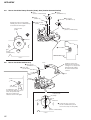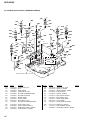
1
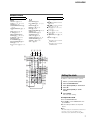
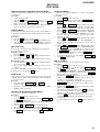
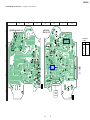
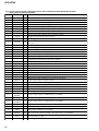
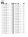
HCD-HP8V
Pin No.
Pin Name
I/O
199
TMODE0
I
Selection signal input terminal for the test Not used
200
AUDDTI
I
Serial audio data input terminal Not used
201
AUDDTO0
O
Serial audio data output to the digital filter
202
AUDDTO1
O
Serial audio data output terminal Not used
203
AUDBCK
O
Serial audio bit clock signal (2.8224 MHz) output to the digital filter
204
AUDLRCK
O
Serial audio L/R sampling clock signal (44.1 kHz) output to the digital filter
205
AUDXCLKO
O
Serial audio clock signal output to the digital filter
206
CLKA
I
Sub system clock input terminal (27 MHz)
207
CLKB
O
Sub system clock output terminal (27 MHz)
208
VDD9
—
Digital power supply terminal (+2.5V) (for CD-DSP block)
209
THRCLK
I
Clock signal input terminal for the test Not used
210
TESTEN
I
Setting terminal for the test Normally: fixed at “L”
211
TCLK
I
Clock signal input terminal for the test Not used
212
TMODE1
I
Selection signal input terminal for the test Not used
213
TRST
I
Reset signal input terminal for the test Not used
214
VSS9
—
Digital ground terminal
215
V AVS1
—
Analog ground terminal (for D/A converter)
216
V AVD1
—
Analog power supply terminal (+2.5V) (for D/A converter)
56
Description