1
I
O P E R A T I N G
A N D
S E R V I C E
M A N U A L
MULTIMETER
3465A
HEWLETT
-
Section III
Model 3465A
S E C T I O N III
OPERATING INSTRUCTIONS
3-1. INTRODUCTION.
3-2. This section contains instructions for using the Multimeter for making dc voltage, ac voltage, dc current, ac
current and ohms measurements. The section also contains
a description of the front and rear panel features.
[wrnnlnc)
To prevent potential electrical or fire hazard,
do not expose the Multimeter or its accessories
to rain or moisture.
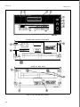
3.3. Front end Rear Panel Features.
3-4. An illustration and description of the front and rear
panels is provided in Figure 3-1. All controls and connectors are identified and briefly described. Some rear panel
features are available with certain options only and are
identified in the description.
3-5. Turn-on and Warm-up.
3-6. For specified measurement accuracy, allow the instrument to warm-up for at least 10 minutes.
Before operating from an ac source, verify that
the 110/220 V line voltage selection switch,
located on the rear panel of the Standard and
Option 001 Multimeter or the Model 82002A
Battery Cargher/AC Adapter, is set to the ac
source voltage to be used.
3-7. Internal Battery Voltage Measurement and Recharging.
3-8. The Multimeter contains a feature allowing the user to
check battery strength to determine the need for battery replacement or recharging. By setting the Multimeter to dc V
Function and the 20 megohm range, the battery voltage is
numerically represented on the Multimeter display. The
decimal point must be moved one place to the right to
derive the actual voltage level from the display (.370 =
3.70 V dc). If the battery voltage drops below a display of
.300 (3 V), the Multimeter will automatically shut down.
A fully charged standard Multimeter will display approximately .380. Fresh batteries in an Option 002 Multimeter
will display approximately ,600. Recharging of the NiCad
batteries is performed by operating the Multimeter on an ac
source (verify line voltage selection switch is in correct position for source voltage used). Measurements can be made
with the Multimeter operated from the ac source during the
recharging period.
NOTE
After 14 hours, a completely discharged battery
will be fully charged. Shorter charge periods
will allow reduced battery operating time.
There is no danger of overcharge. For convenience, ovemigh t charging is recommended
3-9. Low Battery Voltage Detection.
3-10. The Standard and Option 002 Multimeters contain
an internal battery source (Standard contains rechargeable
NiCads; Option 002 contains “D” cell or “U2” batteries).
A battery source safety feature of the Multimeter is a low
battery voltage detection circuit which turns the instrument off when battery voltage reaches a low level. This protects against cell reversal of the NiCad batteries. If during
operation the display disappears or immediately after turnon the display appears and disappears after several seconds,
low battery voltage is indicated. To verify low battery voltage, the procedure described in the preceding paragraph can
be used or verify by placing the OFF/ON switch to OFF
and to ON again. The display will appear and again disappear. Operation from an ac line source and recharging of
the NiCad batteries is required in a Standard instrument.
Replacement of “D” cell or “U2” batteries is required in an
Option 002 instrument.
NOTE
In protecting batteries and circuitry, the low
battery voltage detection circuit may shut
down the instrument if:
1. the power switch is momentarily turned
off then back on, or
2. if a live line power cord is attached to the
instrument while it is operating in the battery mode.
To restore normal operation, the instrument
must be turned off with the front panel power
switch for a minimum of 10 seconds.
3-11 Overload Indication.
3-12. The Multimeter is capable of displaying 19999 for all
functions and ranges. There are maximum voltage limitations in DCV and ACV, however (see ac and dc voltage
measurement paragraphs). In an overload condition where
the input exceeds 19999, the last four digits blank and the
3-l
Section III
Model 3465 A
STANDARD AND OPTION 001 REAR PANEL
/
\
REFER
swvlclNs
TO
OUALWED
PERSONNEL.
. L I N E SELECTOR
ii
0
I
OPTION 002 REAR PANEL
Figure 31. Front and Rear Panel Features.
3-2
\
Model 3465A
Section III
n
Do not apply a voltage greater than + 500 V dc or 500 V peak between
COM terminal and chassis ground or damage to the instrument will
occur.
0
02
1
OFF/ON Switch. Pushbutton push on/push off switch.
FUNCTION Switch. Function markings are located above
each
pushbutton
switch.
- V = DC Volts
“V
= AC Volts
-=A = DC Amps
-A
= AC Amps
S2 = O h m s
0
0
3
4
0
5
Display. Indicates the measured value and polarity of dc
volts or amps.
RANGE Switch. Range markings. are located above each
pushbutton switch. Color bands identify the range switches
associated with each function switch.
DCV/ACV/OHMS
High input terminal.
Symbol. This symbol is an international symbol
@A
meaning “refer to the Operating and Service Manual”. This
symbol will appear in this section of the manual flagging
operating instruction information.
01
08
09
0IO
01 1
0
013
COM input terminal. This terminal is connected to circuit
ground for all measurements except ohms. In the ohms function, the COM terminal is disconnected from circuit ground.
DC/AC AMPS High input terminal. 2 amp fuse located
behind removable “A” terminal cap.
AC power input connector.
Line voltage selection switch.
ZERO ADJ. Internal adjustment used to zero the display in
the DCV FUNCTION, 20 m V RANGE.
12
014
Battery access door (Standard and Option 001).
Battery access door (Option 002 only).
B a t t e r y c h a r g e r ( M o d e l 82002A) p o w e r i n p u t c o n n e c t o r
(Option 002 only).
0
15
Battery access door lock (Option 002 only).
Figure 3-1. Front and Rear Panel Features (cont'd).
overrange “1” and decimal point will be displayed. The
polarity sign is also displayed in the dc volts and dc current
functions in the overload condition.
3-13. AC VOLTAGE MEASUREMENTS.
!
n
B
Maximum input voltage in the ACV FUNCTION is 500 V rms, 800 Vpeak and 600 V dc.
Do not exceed these voltages or damage to the
instrument will occur.
3-14. AC VOLTAGE Ranges.
3-15. The ACV FUNCTION has five ranges from 200 mV
to 500 V. Each range has a maximum display reading of
19999. However, the 500 V range is limited to a maximum
ac input voltage of 500 V.
3-16. DC VOLTAGE MEASUREMENTS.
!
n
m
Do not exceed a maximum input voltage of
1 0 0 0 V (dc + peak ac) on the 1000 V range or
damage to the instrument will occur. There is
no overrange capability on the 1000 V range.
3-17. 20 mV Range Zero Adjust.
3-18. When using the Multimeter on the 20 mV range in
DC volts, short the input terminals and zero the Multimeter
display with the rear panel ZERO ADJ control (see Figure
3-1). The display should indicate 0.000 before proceeding
with measurements.
3-19. DC Voltage Ranges.
3-20. DC Voltage measurements can be made from 20 mV
to 1000 V full-range. Each range has a maximum display
reading of 19999. However, the 2000 V range is limited to
maximum input of 1000 V dc and peak ac (see DC Voltage
measurements caution in Paragraph 3-16).
3-21. CURRENT MEASUREMENTS.
n
Do not exceed a maximum input voltage of
350 V dc and peak ac or a maximum dc or ac
rms input current of 2 A or the amps fuse,
located directly behind the “A” terminal, will
open. See the following paragraph for replacement instructions.
3-3
Model 3465A
Section III
3-22. The Multimeter is protected from the application of
excessive current by a 2 A fuse located directly behind the
front panel “A” terminal. If it is necessary to replace this
fuse, use the side slots on the “A” terminal to rotate the
terminal. The terminal and fuse will protrude from the
front panel. Remove the terminal and fuse, replace fuse
with a 2 A rated fuse as listed in Table 6-3 Miscellaneous
Parts General, and designated Fl.
3-23. AC Current Ranger
3-24. AC current measurements are specified over a frequency range of 40 Hz to 20 kHz. There are five current
ranges from 200 MA to 2000 mA. See current measurements Caution in Paragraph 3-2 1.
3-25. DC Current Ranges.
3-26. DC Current measurements can be made on five current ranges from 200 /.tA to 2000 mA. See current measurements caution in Paragraph 3-21.
3-27. OHMS MEASUREMENTS.
Q
H
Do not apply voltage greater than 2 350 V dc +
3-4
Peak AC between the ohms and common input
terminals in the ohms function or damage to
the instrument will occur.
3-28. Ohmmeter Hanger
3-29. Resistance measurements can be made on six ranges
from 200 ohms to 20 megohms. Both input terminals (Ω
and COM) are floating with respect to circuit ground.
3-30. Ohmmeter Reference Current
3-31. The ohmmeter reference current through the unknown resistance for each range is shown in Table 3-l.
Table 3-1. Ohmmeter Current Through Unknown.
Current
Through Unknown
200 51
2 kS1
20 M
200 kc2
2000 k&-2
20 m-2
1 mA
1 mA
lOpA
lOpA
1 MA
0.1 PA
Maximum open-circuit voltage at the ohms input terminals
is less than 5 V.
Model 3465 A
Section
IV
SECTION IV
THEORY OF OPERATION
4-1.
INTRODUCTION.
4-2. This section contains the theory of operation for the
Multimeter. The information is divided into two parts:
1. Simplified Theory
2. Detailed Theory
The simplified theory provides an overview of the operation
of each section in the Multimeter while the detailed theory
describes the circuit operation of each section.
4-3. Description.
4-4. The Multimeter is a five-function, 4-1/2 digit multimeter. The five functions measured are dc volts, ac volts,
OHMS REFERENCE
dc current, ac current and ohms. The dual-slope integration technique is used for measurements. This technique
charges an integrator for a fixed length of time, to a voltage
proportional to the input signal, then discharges the integrator at a fixed rate determined by a known reference voltage. The measurement display is determined by the discharge time of the integrator, which is proportional to the
input signal.
4-5. Figure 4-1, Basic Block Diagram and Measurement
Sequence, illustrates the major functional blocks of the
Multimeter. The illustration of the measurement sequence
shows the integrator output for each interval of a measurement cycle. This diagram is to supplement the functional
block diagram for the simplified theory discussion.
41
RUN-DOWN
REFERENCE
INPUT
-
SELECT
DISPLAY
CONDITIONING
AUTO-ZERO
CONTROL
INPUT/ZERO
ADJ CONTROL
3465-B-4166
> HALF - SCALE INPUT - r\
/ ’\
;
lN;;F;.AfOR
HALF-SCALE
INPUT
,’
/
\
\
\
NOTE
NEGATIVE INPUTS ILLUSTRATED;
FOR POSITIVE INPUTS THE
WAVEFORMS ARE INVERTED.
\
//
’
/’
<HALF-SCALE INPUT ,,‘,//
REF%?
‘1 \
‘\
\
\
\
\
NCE
’
/8- AUTO-ZERO +Q
MEASUREMENT SEPUENCE INTERVALS
Figure 4-1. Basic Block Diagram and Measurement Sequence.
Section IV
Model 3465A
4-6. SIMPLIFIED THEORY.
4-7. A simplified theory of operation of the Multimeter is
presented in the following paragraphs. The simplified
theory describes each section of the functional block
diagram, Figure 7-1. These sections are the signal conditioning section, analog-to-digital section, logic section and
the display section. Also presented is a simplified description of the power supply. Refer to Figure 7-1, Functional
Block Diagram, and Figure 4-1, Basic Block Diagram and
Measurement Sequence, for this discussion.
4-8. Signal Conditioning.
4-9. Signal conditioning consists of attenuating and/or
converting the input signal to a dc voltage within the
working limits of the input amplifier. For half-scale inputs,
this voltage can vary from 20 mV dc to 2 V dc depending
on the function and range.
4-10. The signal conditioning section consists of current
shunts, an input attenuator, ohms converter and an
ac-to-dc converter. The output from the signal conditioning section is applied to the input amplifier during the
run-up interval of the measurement sequence. The Input
Amplifier Gain Table located on Figure 73 indicates the
half-scale input level applied to the input amplifier for each
function and range. This signal is the output of the signal
conditioning section.
4-11. Ohms Converter. The ohms converter is a high gain
integrating amplifier. A simplified diagram of the ohms
converter is presented in Figure 4-2. The blocks of the
ohms converter are the integrating amplifier, protection
diodes, over-voltage protection circuit and the overload
loop. An integrating amplifier is used because this type of
amplifier is less susceptible to oscillations. The protection
diodes clamp the a terminal to a voltage of about 1.2 V
in the positive direction or 0.7 V in the negative direction.
With the Q terminal clamped, protection against excessive
voltages applied to the ohms terminals is provided by an
over-voltage protection circuit located between the ohms
amplifier and the terminal. For excessive voltages, this
circuit isolates the COM terminal from the ohms amplifier.
4-12. Figure 4-2 shows two outputs of the ohms converter
being applied to the input amplifier. The ohms output is
the ohms converter measurement signal and the auto-zero
output is the ohms amplifier dc offset signal which is called
the auto-zero (AZ) signal. This AZ signal is applied to the
input amplifier during the auto-zero interval of the measurement sequence and establishes the reference for the
analog-to-digital converter. An AZ signal greater than
f 1 mV causes the instrument readings to be invalid. This
condition (AZ signal > f 1 mV) is present when the
unknown resistance, R,, is removed and an open loop is
present on the ohms amplifier. To maintain the AZ signal at
< f 1 mV when an open loop is present, an overload
feedback circuit is used.
4-13. The ohms output, (LO terminal of the ohms converter) is applied to the input amplifier. This output is a dc
voltage, the level of which is dependent on the ratio of the
unknown resistance, R,, to the variable resistance, lo”, and
the ohms reference supply. The variable resistance, lo”, is a
resistor string located in the precision resistor pack R75.
The value of 10” is selected by the range switches shorting
those resistors in the string that are not required. The value
of 10” can range from 10 ks2 to 10 m. A discussion of the
precision resistor pack R75 can be found in the detailed
theory.
4-14. The formula for the ohms converter output voltage
is:
1
]
Ohms
R,
output = - En
Voltage
Reference Supply Voltage + Voftset
AUl$X&RO
c29
(b
2’
av IS
~“~RT’wAL
*+IV F O R
IOM RANGE
OVERVOLTAGE
PROTECTION
CIRCUIT
_
Figure 4-2. Simplified Diagram, Ohms Converter.
4-2
OHMS
OUTPUT
Model 3465 A
Section IV
The reference supply is + 10 V for all ranges except the
20 M range. For this range the reference supply is + 1 V.
On the 20 M range with an Rx of 10 MSZ, an output of 1 V
dc is needed. From the formula for the ohms output, it
can be seen that 10n would have to equal 100 M!L Since
the range of 10n is 10 kS2 to 10 M8, a 10n of 10 Ma
combined with a reference supply of 1 V provides the desired 1 V dc full-scale ohms converter output.
4-15. AC-DC Converter. The ac-dc converter is an average
responding ac converter. It measures the average value of a
sine wave and multiplies this by a fixed scale factor to
convert it to an rms value. The output of the converter is a
dc voltage equal to the rms value of the sine wave.
4-16. Figure 4-3 is a block diagram of the ac-dc converter.
The blocks consist of an impedance converter, an ac
converter and a filter. The impedance converter has a high
input impedance to prevent loading of the input signal. It
also provides the gain necessary to drive the ac converter.
An impedance converter gain of unity, 9.964 or 10 is
selected by the function and range switching. The gain of
9.964 is used with the ac current function and the gain of
10 is used with the 200 mV, .2 mA, 200 Sz and 20 V,
20 mA, 20k!G? ranges.
4-17. The ac converter amplifies the signal from the
impedance converter by the scale factor. This converts the
average value of the sine wave to the rms value. Half-wave
rectification of the sine wave is also performed by the ac
converter. This rectified signal is filtered to provide the
proportional dc output which is applied to the analog-todigital converter.
4-18. Analog-to-Digital (A-D) Converter.
4-19. The A-D converter block is comprised of an input
amplifier, reference supply, integrator, slope amplifier,
comparator and auto-zero circuit. It makes an analog-todigital conversion using the dual-slope integrating technique. Four control state signals from the logic section (IO,
IZ, I1 and I2) regulate the measurement sequence. IO and
IZ regulate the input amplifier and auto-zero switching
respectively while I1 and I2 select the reference supply
required during the run-down interval.
The first stage of the A-D converter is the input amplifier. During the run-up interval of
the measurement sequence, control state signal IO switches
the output of the signal conditioning block to the input
amplifier. The output of the signal conditioning block is a
dc voltage which varies between 10 mV and 1 V for
half-scale inputs, depending on the function and range
selected. The gain of the input amplifier is adjusted by the
function and range switching to provide an output of 1 V
dc for any half-scale input signal. See Input Amplifier Gain
Table on Figure 7-3.
4-20. Input Amplifier.
The A-D converter uses a monopolar reference supply of + 10 V. A reference voltage is
applied to the integrator during the rundown interval to
discharge the integrating capacitor. Since the discharge rate
is constant, the time required for the integrator to reach a
zero reference is proportional to the input signal. This time
period is the run-down interval and is processed to
determine the display. A positive and negative reference
voltage is required since the input signal can be either
polarity. A detailed discussion of the operation of the
monopolar reference supply can be found in the detailed
theory.
4-21. Reference Supply.
4-22. Integrator. The integrator output is a result of a
current summation at the integrator summing junction
(inverting input). A positive current summation (current
flowing into the integrator input) will cause the integrator
to ramp negative. A negative current summation (current
flowing out of the integrator input) will cause the integrator to ramp positive. The integrator sums currents from the
input amplifier, reference supply, - 7 V supply and the
auto-zero loop during designated times.
4-23. Slope Amplifier. Following the integrator is a X4000
amplifier. This amplifier is divided into two stages; the first
with a gain of 40 and the second with a gain of 100. The
slope amplifier amplifies the integrator output to provide a
more vertical crossing of this output with the reference
level. This provides greater accuracy of the voltage-totime conversion during the rundown interval.
The comparator provides two logic
outputs; a high output of 0 V or a low output of - 7 V. The
comparator output is high when the integrator output is
greater than the reference level. The comparator is low
when the integrator output is less than the reference level.
4-24. Comparator.
IMPEDANCE
CONVERTER
Figure 4-3. Block Diagram, AC-to-DC Converter.
4-3
Section IV
This logic level is sensed by the logic section to determine
polarity and zero-detect.
During the measurement sequence, the auto-zero loop is closed except for the run-up
and run-down intervals. This loop includes the slope
amplifier and the integrator but does not physically include
the input amplifier although the loop does compensate for
the input amplifier offset. When the auto-zero loop is
closed, the input of the input amplifier is grounded. If the
summation of currents at the integrator summing junction
is not zero, the integrator begins to ramp up for a negative
summation or ramp down for a positive summation. The
integrator output is applied through the X4000 slope
amplifier to the auto-zero capacitor, C4. The voltage on the
auto-zero capacitor causes a current to flow at the summing
junction that returns the summation to zero. This auto-zero
configuration compensates for the analog offset of the
input amplifier and integrator by providing a current at the
summing junction that cancels the currents resulting from
the offset.
4-25. Auto-Zero Circuit.
4-26. Logic Section.
4-27. The Logic Section is comprised of combinational and
state logic. This section processes the comparator output to
determine the polarity of the input signal and to make a
voltage-to-time conversion of the input signal. Time
accumulated during the conversion is proportional to the
input signal and is stored. The display is derived from this
accumulated time. A voltage-to-time conversion with the
accumulated time being stored occurs once each measurement sequence.
4-28. Seven blocks make up the logic section. These blocks
are:
1. Clock
2. State Clock
3. Polarity and Zero Detect
4. Data Transfer and Reset
5. Control State Counter
6. Control State Decode
7. Data Accumulator
The HIGH and LOW logic levels used in the logic section
are 0 V and - 7 V respectively. The following discussion
describes the basic operation of the logic section.
The timing of the logic
section is derived from the clock circuit. The clock operates
at 100 kHz and is crystal-controlled. A state clock, driven
by the clock output and the count extend line from the
data accumulator, drives the control state counter to
initiate each measurement interval.
4-29. Clock and State Clock.
4-30. Polarity and Zero Detect. The polarity and zerodetect circuit monitors the comparator output. The state of
this output at the beginning of the rundown interval
determines the polarity of the input signal. Zero-detect is
determined at the point the comparator output changes
states during the run-down, overrange or overflow intervals.
Model 3465A
If the integrator ramps positive (negative input signal)
during run-up, the comparator output goes HIGH and
returns to LOW at the zero-detect point. If the integrator
ramps negative (positive input signal) during run-up, the
comparator output goes low and returns to high at the
zero-detect point. These comparator output logic states are
stored in a D flip-flop. At the beginning of the rundown
interval, this state identifies the polarity of the input signal.
The outputs of the D flip-flop provide the signals needed
to select the correct polarity display and the correct
reference supply signal (I1, I2) during the rundown
interval. An EXCLUSIVE OR and latch processes the
comparator output to provide the zero-detect signal.
The data transfer and reset
circuits provide logic signals to the data accumulator
required to load the storage latches and reset the decade
counters. A detailed description of the data accumulator is
provided in the detailed theory section. While the %%
input of the data accumulator is low, data in the decade
counters is transferred to the static storage latches. The
RESET input resets the decade counters to zero when low.
This must occur after the transfer to the storage latches has
taken place. To ensure that reset occurs after termination
of transfer, an RC delay circuit precedes the reset gates.
4-31. Data Transfer and Reset.
The control state counter
provides the timing for the measurement sequence intervals.
The output from the counter establishes the timing of the
analog control signals (IZ, IO, I1 and I2) which are applied
to the A-D converter. The state clock and reset inputs to
the control state counter determine the outputs of the
counter.
4-32. Control State Counter.
The control state decode
converts the polarity, zero-detect and control state counter
inputs to the correct analog control signals. These signals,
applied to the A-D converter, perform the measurement
sequence switching. This switching consists of the input
amplifier switch, the auto-zero switch and the reference
supply switches.
433. Control State Decode.
434. Data Accumulator. The data accumulator consists of
a counter, data latches, a multiplexer, digit select decoder
and output buffers. At the beginning of the Run-Down
interval of the measurement sequence, the data accumulator begins to count clock pulses until zero-detect occurs.
This count is proportional to the input signal and is the
time conversion used to generate the display. The digit
select decoder scans the display digits from the most
significant digit to the least significant digit while the
multiplexer provides the corresponding BCD outputs for
each digit. A detailed discussion of the data accumulator is
presented in the detailed theory.
435. Display.
4-36. The multimeter display contains four full digits with
an overrange “1” and polarity sign. All segments and indicators are light-emitting diodes. A BCD-to-seven segment
decoder receives BCD information from the data accumu-
Model 3465A
Section IV
lator and applies the seven-segment code to the display
drivers. The display drivers apply the seven-segment code to
all digits simultaneously. Digit strobe lines activate the digit
corresponding to the seven-segment code at that point in
time. Scanning of the digits is from the most significant to
the least significant digit. To complete the display. the
proper decimal point is enabled by range switching.
4-37. Power Supply.
4-38. Figure 4-4 is a block diagram of the power supply.
The power supply develops four output voltages from a
single dc input voltage (+ V,). This dc input voltage is
applied to a dc-to-dc converter which develops output
voltages of + 11 V dc and - 7 V dc. A series regulated
+ 10 V output is developed from the + 11 V converter
output. This + 10 V is used as the reference voltage in the
A-D converter and to develop the reference current in the
ohms converter and as the reference voltage for the
converter regulator. The converter regulator controls the
converter and regulates the - 7 V and + 11 V outputs of the
converter. A discussion of the operation and regulation
process of the dc-to-dc converter is presented in the
detailed theory.
I+“”
0
+ ,,, - dc-lo-dc
CONVERTER
-
-
SERIES
VOLTAGE
REGULATOR
CONVERTER
REGULATOR
t
1
I
I
+10V
-7”
Figure 4-4. Block Diagram, Power Supply.
4-39.
DETAILED
THEORY.
maintain the accuracy of the Multimeter. These resistances
are part of the resistor pack. The advantage to the resistor
pack is high precision resistors- and good temperature
tracking. As resistance values of the resistor pack change
due to temperature changes, the ratio of the resistors
remains the same.
4-43. Ohms Converter.
4-44. Refer to Figure 7-2 for this discussion. Both ends of
the ohms converter are floating with respect to the
instrument ground. The unknown resistor, R,, becomes the
feedback loop of the ohms amplifier. The ratio of R, to
10n determines the gain of the ohms amplifier, Q25 and
U15. 10n is a variable resistance between 10 ka and 10 M8
selected by the range switching. The ohms converter input
is the reference voltage provided by the ohms reference
supply. This reference voltage times the amplifier gain is the
ohms converter output supplied to the input amplifier
during the run-up interval. Half-scale ohms converter gain
and output values are provided in the ohms converter table
located on Figure 7-2.
4-45. The n HI LEAD of the ohms converter is connected
to the reference supply through 10n of the resistor pack
R75. The s2 HI LEAD is clamped by protection diodes
CR15 and CR25 to prevent the destruction of FET Q25
and R75 by the application of large voltages. These diodes
Clamp the a HI LEAD to about 1.3 V positive or 0.7 V
negative.
4-46. With the R HI LEAD clamped. over-voltage protection must be provided to protect the ohms amplifier from
excess voltage. The over-voltage protection circuit is located
between the ohms amplifier and the LO terminal point and
is shown in Figure 4-5. During normal operation < 2 mA of
current flows through Q30, R94 and Q32. If a large voltage
is applied to the ohms terminals, the current through this
circuit will try to exceed 2 mA. This current will cause a
large enough voltage drop across R94 to turn on Q31. When
Q31 is on, it removes the base drive from Q30, which turns
off, disconnecting the LO terminal point from the ohms
converter. Since Q30 is a high voltage transistor, large
voltages are not applied to the ohms converter.
+ IO”
LO
4-40. This portion of the theory of operation provides a
detailed discussion of the circuits in the Multimeter. The
circuits described here are the ohms converter, ac-dc
converter, monopolar reference supply, data accumulator
of the logic section, display and the power supply. A
discussion of the precision resistor pack (R75) is also
provided. The detailed discussion makes use of the schematics in Section VII.
TERMINAL
POINT
OHMS
OUTPUT
f
4-41. Precision Resistor Pack (R75).
4-42. The precision resistor pack, R75, is a laser trimmed
substrate providing high precision resistances. A diagram of
R75 is shown on Figure 7-2. The input attenuator, power
supply, ohms reference supply, A-D reference supply and
the input amplifier require highly accurate resistances to
FROM
OHMSAMPLIFIER
Figure 4-5. Over-Voltage Protection Circuit.
4-5
Model 3465 A
Section IV
4-47. In the event of open loop (Rx = -), the ohms
amplifier output begins to drive negative. The input
(negative port), which is the auto-zero output, could exceed
f 1 mV under an open loop condition due to the lack of
negative feedback through an Rx. This auto-zero output
must be maintained at Q f 1 mV for accurate operation of
the A-D converter. To satisfy this requirement, an overload protection circuit consisting of CR23, CR24 and R86
is used. When the ohms amplifier output goes below
approximately + 1.5 V, the zener diode (CR23) turns off.
The overload loop, CR24 and R86, is introduced by the
turn-on of CR24 when CR23 is off. This loop provides the
negative feedback required to maintain an auto-zero output
< f 1 mV. When an R, is introduced, CR23 turns-on,
CR24 turns-off, and the overload loop is inoperative.
4-48. A maximum output by the ohms converter of Q 5 V
is guaranteed by a voltage divider composed of R93 and
R95. Additional protection components of the ohms
converter are: A) CR29 which prevents Q32 junction
breakdown due to fast transients, B) CR28 which blocks
negative transients that could come in via the LO terminal
point and C) R91 and C27 which suppress high voltage,
high frequency transients.
4-49. Degradation of accuracy in the ohms function due to
changes in the ohms reference with respect to the A-D
reference is minimized since both reference voltages are
derived from the same t 10 V reference supply. If the
reference supply voltage changes, both the ohms reference
and the A-D reference are affected alike and any change is
effectively cancelled.
4-50. AC-to-DC Converter.
4-51. The AC-to-DC converter is an average responding
ac converter. It has a bandwidth of 40 Hz to 20 kHz. The
converter is composed of two stages (see Figure 7-2). The
first stage, U19, is an impedance converter. The purpose of
this amplifier is to provide a high impedance to the input so
loading of the input signal does not occur. It also provides
high drive capability for the ac converter stage, U18. The
input of the impedance converter is protected against large
voltage swings by diodes CR35 and CR37. Voltages in
excess of + 10 V or - 7 V peak ac will forward bias these
diodes, returning excess current to the power supply.
4-52. The impedance converter, U19, has a selection of
three gains; the 200 mV, .2 mA, 200 S! and 20 V, 20 mA,
20 ka ranges select a gain of 10. The ac current function
selects a gain of 9.964, while the remainder of the ranges
and functions select a gain of unity (see U19 Gain Table,
Figure 7-2).
4-53. The second stage of the AC-to-DC converter is the
ac converter, U18. A basic diagram of this stage is shown in
Figure 4-6. The amplifier has three feedback loops. These
loops are the ac negative feedback loop, the dc negative
feedback loop, and the positive feedback loop. The ac
negative feedback loop is divided into two branches; one
branch for the positive half cycle and the second branch for
the negative half cycle. Diodes CR33 and CR34 switch
4-6
,
AMP
R125
220K
AC
NEGATIVE
FEEDBACK{
LOOPS
CR33
v
.
R127
220K
CR34
‘I
41
Figure 4-6. Basic Diagram, AC Converter Amplifier.
between the positive and negative half-cycles to introduce
the correct loop for its respective half-cycle.
4-54. During switching of the diodes, little negative feedback is present. During the switching transition, the positive
feedback loop (C45, R120 and R123) boosts the amplifier
gain. This boost in gain speeds the switching transition of
the diodes which gives a good frequency response at low
signal levels. Once the switching transition has occurred,
negative feedback’ is again present. The negative feedback
overrides the effects of the positive feedback loop at all
times other than the diode switching transition period.
4-55. The output of the AC-to-DC converter is derived
from the positive half-cycle, negative feedback loop. The
positive half-cycle developed across the load resistor R118
is the half-wave rectified signal of the ac converter amplifier
output. This rectified signal is filtered to provide the dc
output that is applied to the input amplifier during the
run-up interval of the measurement sequence. For half-scale
inputs, the ac-to-dc converter output is 0.8 V dc. This
output is kept relatively free of the dc offset present on the
inverting input of U18 (pin 2) by the voltage divider R125
and R118. The portion of the offset appearing across the
load resistor R118 is attenuated by a factor of 23.
4-56. A-D Conversion Using a Monopolar Reference.
4-57. Before preceeding with this discussion, review the
Model 3465A
Section IV
A D converter description of the integrator, slope amplifier and auto-zero circuit in the simplified theory. Figure
4-7, Functional Diagram, A-D Converter, illustrates these
circuits in relation to the monopolar reference supply, the
input amplifier and the comparator. It also illustrates the
integrator output and the four control state signals, IZ, IO,
I1 and I2, with respect to the measurement sequence
intervals.
MONOPOLAR
REF SUPPLY
+10V
INPUT AMP
COMPARATOR
-NOTEA-D CONVERTER
SHOWN IN AUTOZERO MODE
INTEGRATOR
OUTPUT
\
\
/
\
/=n yi&V’
\
/
ON= OV
OFFS -7V
IZ ON
OFF
IO
I1
I2
I
ON
I
OFF
ON
OFF
I
I
L---------J
ON
OFF
------we
STATE OF
CURRENT SWITCH
MEASUREMENT
INTERVAL
AUTO-ZERO
RUN-UP
RUN-DOWN
INPUT
SIGNAL
POLARITY
+
CLOSED
OPEN
-
CLOSED
OPEN
+
CLOSED
OPEN
-
CLOSED
OPEN
I1
I2
+
OPEN
OPEN
-
CLOSED
CLOSED
Figure 4-7. Functional Diagram, A-D Converter.
4-7
Section IV
4-58. The A-D converter of Figure 4-7 is shown in the
auto-zero mode. The input amplifier is grounded at the
input, control state switch I1 is closed, I2 is open and the
auto-zero loop is closed. Note that the auto-zero loop does
not include the input amplifier but is connected to the
integrator summing junction (integrator inverting input).
Also connected to the summing junction are the input
amplifier output, two current paths from the monopolar
reference supply and the - 7 V supply through R59 and
R43.
4-59. The auto-zero loop uses a current balancing technique at the integrator summing junction to establish the
reference. The basic principle is that the algebraic sum of
currents at the integrator summing junction must be equal
to zero. When the sum is zero, the output of the integrator
will not change. If the sum is not zero, the integrator will
ramp up for a negative current or ramp down for a positive
current because of the inverting input.
4-60. When the auto-zero loop is closed, the currents
summed at the integrator summing junction come from
four sources; 1) the output of the input amplifier with its
input grounded, 2) one current path of the monopolar
reference supply (switch I1 closed), 3) the - 7 V supply
through R43 and R59 and 4) the auto-zero loop. The input
amplifier output is the analog offset of this amplifier. The
current due to the - 7 V supply is roughly the negative of
the current from the monopolar reference supply. The
auto-zero loop then stores a voltage on the auto-zero
capacitor that produces a current through R28 and R42 of
the correct magnitude to force the summation of currents
at the integrator summing junction to zero. Forcing the
summation of currents to zero compensates for the analog
offset of the input amplifier and integrator.
4-61. During the run-up interval, the auto-zero loop is
opened by control state switch IZ. The voltage stored on
the auto-zero capacitor is still applied to the integrator
summing junction and the summation of currents remains
zero. At the time the auto-zero loop is opened, the output
of the signal conditioning section is switched to the input
amplifier by control state signal IO. The output of the
input amplifier causes the algebraic summation of currents
at the integrator summing junction to deviate from zero.
This causes the integrator to run-up.
4-62. At the end of the run-up interval, the input amplifier
is switched back to ground by control state signal IO. The
summation of currents at the integrator summing junction
is again zero and if no other action were taken, the
integrator output would not change. The integrator output
is positive at the end of run-up for negative inputs and
negative for positive inputs. At the end of the run-up
interval, the polarity of the integrator output is determined
by the logic section. This also identifies the polarity of the
input signal.
4-63. At the beginning of the run-down interval, the logic
section selects the appropriate reference to return the
4-8
Model 3465A
integrator output to zero. Run-down uses the summation of
currents principle at the summing junction of the integrator. The two current paths (I1 and I2) of the monopolar
reference supply provide the means of changing the
summation of the currents. The summation of currents at
the summing junction can be made negative by opening
switch I1 and removing this current flow to the junction.
The summation can be made positive by closing switch I2
in addition to I1, and providing twice the current from the
monopolar reference supply. Opening switch I1 with I2
open, runs the integrator up which is required for positive
inputs (see Figure 4-7). Closing I1 and I2 runs the
integrator down which is required for negative inputs. The
time required for the integrator to reach zero-detect during
the run-down interval is proportional to the input voltage
which caused run-up and determines the display.
4-64. Data Accumulator.
4-65. Refer to Figure 4-8, Data Accumulator Diagram, for
this discussion. The data accumulator processes the logic
signals from the logic section and provides the BCD output
and the scan signals that determine the dsiplay. The data
accumulator consists of a counter, data latches, a multiplexer, digit select decoder and, output buffers. At the
beginning of the measurement, the reset signal (RESET)
goes to a logic 0 to initialize the counter and digit select
decoder. At the beginning of the rundown interval of the
measurement sequence, the counter begins to accumulate a
count proportionalto the run-down time.
4-66. The counter consists of four divide by 10 circuits.
The output of each circuit is a BCD number representing
one digit of the input signal. At the end of the rundown
interval, the transfer signal (TXFR) is set to a logic 0. This
stores the counter outputs in the data latches.
4-67. The scan signal will gate each BCD signal from the
latches, beginning with the most significant digit first,
through the multiplexer to the output. At the same time
that the scan gates the digits through the multiplexer, the
gaiing signal is output to the display as a digit activation
pulse.
4-68. The BCD output of the multiplexer
- is applied to the
display, section (see Figure 74). The BCD is applied to quad
NAND gates in the display section where the m logic is
converted to BCD logic. The BCD is applied to the seven
segment decoder where it is transformed to a seven bit
binary number and applied to each numeral in the display.
As the digit activation pulse from the data accumulator
sequentially activates each numeral from most significant to
least significant, the seven bit binary data will be displayed.
4-69. Display.
4-70. Refer to Figure 7-4 for this discussion. The display
segments are powered by a + 3 V supply. This voltage is
Model 3465A
Section IV
DIGIT
ACTIVATION
TO DISPLAY
m BUFFER .
OUT
) BUFFERS -BcD
TO DISPLAY
I
DIGIT
S C A N - SELECT
DECODER
@
MULTIPLEXER
4
A
A
TXFR
-w
A
LATCHES
A
RESET
AA’
4
AA
,COUNT
EXTEND
- COUNTER
t
CLOCK
(100kHz)
3465-R-4174
Figure 4-8. Data Accumulator.
derived from V, and the + 11 V output of the power
supply. A series voltage regulator, Q21, Q22 and Q23
maintains the + 3 V output constant. This provides constant display intensity for changes in the magnitude of VB
due to battery life and results in low power consumption
for a high VB (new or recharged batteries).
4-71. Twenty-five connections interface the display and
the main assembly. Table 4-1 indicates each terminal and
the source of the signal from the main assembly.
Table 4-1. Display interface Connections.
I
I
I
CONNECTION
DESIGNATION
I
SOURCE OF SIGNAL
DIGIT STROBES: MSD, 2MSD, 3MSD, LSD
BCD: 1, 2, 4, 8
DATA ACCUMULATOR
(A1U11)
DECIMAL POINT: A, B, C, D
RANGE SWITCHES
POLARITY ENABLE: E
POLARITY:
PL
I
FUNCTION SWITCHES
I
Al U4
I
I
LOGIC
OVERRANGE: OR
OVERLOAD:
OL
TRANSFER: TXFR
+ VB, + 11 V, GND, - 7 V, - 7 VF
PIN 25
Al U5
SECTION
Al U6
POWER SUPPLY
NO CONNECTION
I
4-9
Section IV
Model 3465A
Figure 4-9. Basic Diagram, DC-to-DC Converter.
4-72. Power Supply.
4-73. The method by which a dc-to-dc converter produces
a negative output voltage from a positive source voltage can
be explained with the aid of Figure 4-9. The switch S opens
and closes with a given duty cycle. For steady-state conditions, the output voltage will be related to the duty cycle of
the switch by:
Both V and L are fixed, so the inductor current increases
linearly with time. This results in an energy transfer from
the battery to the inductor. When switch S is opened during
toff, current flow to the inductor is shut off. Because the
fundamental characteristic of an inductor is to oppose any
change in current flow, the inductor generates a back emf
of approximately -8 volts. This voltage forward-biases
diode CR and allows the energy stored in the inductor to be
transferred to the capacitor and the load.
ton = time switch S is closed
vo=-ton VB
toff
toff = time switch S is open
ton
ton + toff
Changes in input voltage VB can be compensated for by
varying the duty cycle of the switch. This is what is done in
a dc-to-dc converter. When the switch is closed during ton,
diode CR is reverse biased by the negative voltage on its
anode and the positive voltage on its cathode; this isolates
the inductor from the capacitor C and the load. The capacitor keeps the output voltage from dropping to zero during
ton. Closing the switch applies the battery voltage VB
across the inductor. Since the voltage across an inductor is
given by V = L AilAt, the expression for the change in inductor current is given by:
Duty cycle =
1,
4-74. The following paragraphs describe the operation of
the actual dc-to-dc converter circuit in the 3465B, and the
converter regulator. Figure 4-10 shows a simplified schematic of the -7 volt converter and regulator U17. The
discussion assumes steady-state conditions, and begins with
Q33 in the off state (Ic = 0). When Q33 first turns on, it
will be in saturation (see Figure 4-11), causing the entire
voltage + VB to be dropped across the primary of the autotransformer T1. As explained in paragraph 473, the collector current through the inductor begins to rise linearly
with time. The constant voltage at the base of Q34 causes
Q34 and R98 to provide a constant current sink for the
base current of Q33. Consequently, the rising collector
current of Q33 follows one of the Ib curves in Figure 4-11.
Q33 will eventually come out of saturation as the collector
current approaches fllb. When Q33 comes out of saturation,
Ai=t ∆ t
JJ-- Iour -I
c)
3 l7)=+llV
@
NP
;;f;C25
-7\
, 1 v
DI
1.. IC
I”
I
Q
CURRENT
Figure 4-10.
4-10
I1
rCR32
“+,,-h-VI-O.6
I
3-6 +”
VOLTS
Simplified Diagram, DC-to-DC Converter.
Model 3465 A
Section IV
1
Ibl
gr b2
b1 b 3
81 b 4
VCE
-SATURATIOEI
R E G I O N
--&---
A C T I V E
I
R E G I O N - - - - y
1 E X P A N D E D VCE S C A L E 1
Figure 4-11. Common-Emmitter Output Characteristics.
Vce begins to increase, which in turn causes less voltage to
be dropped across the primary of T1. The autotransformer’s windings are such that the primary and induced secondary voltages are 180° out of phase. Therefore, the falling
voltage across the primary causes a rising voltage across the
secondary, which is coupled back to the base of Q33 by
R81 and C25. When the base of Q33 goes sufficiently
positive to reverse-bias the base-emitter junction, Q33 shuts
off and stops delivering current to T1. The primary of T1
then generates a back emf of approximately -8 volts in an
attempt to keep the inductor current from changing. This
action forward biases CR32 and the energy stored in the
magnetic field of the inductor is transferred to C34 and the
load. The -8 volts on the primary of T1 induces +8 volts
on the secondary winding which, when applied to the RC
feedback network, causes the voltage at the base of Q33 to
ramp down. When the base voltage of Q33 drops to (VB-.6)
volts, the base-emitter junction becomes forward biased,
Q33 turns on, and the cycle begins again.
4-75. The secondary winding of T1 is also used to provide
a +11 volt output, which is then further regulated by the
+10 volt series regulator (paragraph 4-77). A positive output is developed by transformer-coupling a portion of the
energy stored in the primary winding inductance through
the secondary winding of T1. This output is equal to the
turns-ratio times the voltage across the primary of T1 when
Q33 is off.
4-76. Changes in the output voltage and in the battery voltage VB can be regulated by varying the duty cycle of transistor switch Q33 (see paragraph 4-73). The duty cycle can
be varied by controlling the voltage at the base of Q34,
which determines the base current of Q33. A larger base
current will cause Q33 to take a longer time to come out of
saturation (see Figure 4-11), which varies the transistor on
time. The voltage at the base of Q34 is supplied by U17.
The inverting input of U17 is grounded through R116,
while a 10-to-7 voltage divider (R117 & R114) is connected
to the non-inverting input. One end of the divider (R117)
senses the voltage output of the +10 volt series regulator,
while the other end (R114) senses the -7 volt output of
the dc-to-dc converter. A change in voltage at the -7 volt
output is sensed by the non-inverting input and is amplified
by U17. The output voltage of U17, driving the base of
Q34, controls the base current of Q33, and regulation of
the -7 volt output is achieved. Since the +11 volt output is
the transformer turns-ratio times the -7 volt output, the
+11 volt supply is also regulated.
4-77. + 10 V series Voltage Regulation.
4-78. The temperature compensated zener diode CR17 is
the voltage reference from which the +10 V reference is
derived. The zener voltage is applied to the non-inverting
input of U16. A resistor divider in the precision resistor
pack (R75) senses the voltage at the output. A portion of
the voltage is fed to the inverting input of U16. This error
voltage is amplified by U16 to drive Q26. The collector
current of Q26 then provides base drive for the series pass
transistor Q26. To ensure turn-on of the dc-to-dc converter,
the collector, as opposed to the emitter of the series pass
transistor Q27, is connected to the output. The low collector-to-emitter satuation voltage aids in the turn-on
process of the converter. This ensures start-up for battery
voltages as low as 2 to 3 volts. One advantage to this configuration is that the +11 V supply can decrease to within
the collector-to-emitter saturation voltage of the +10 V
regulated output and regulation is still maintained.
4-79. Battery Low-Voltage Detection.
4-80. Refer to the power supply schematic, Figure 7-5. The
battery low-voltage detection circuit is comprised of a differential amplifier, Q36 and Q37. The voltage at the base of
Q36 is set at about +2.9 V by the voltage divider R139 and
R141. If the battery voltage (+VB) is greater than +2.9 V,
Q36 conducts and Q37 is off. When the battery voltage
drops below +2.9 V, Q37 turns on providing base drive for
Q38. When Q38 is on, the base of Q34 is pulled to -7V and
Q34 turns off. This action turns the dc-to-dc converter of
the power supply off removing all power supply outputs.
This removes the front panel display indication. To reinstate the display, the OFF/ON switch must be turned OFF
and again ON. The display indication will reappear while
capacitor C51 charges to + 2.9 V. When the voltage on C51
(which is the base voltage of Q36) exceeds the battery voltage (+ VB), the circuit deactivates the power supply as previously described and the display indication disappears
again.
4-11/4-12