1
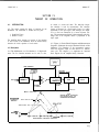
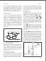
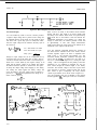
Section IV
4-58. The A-D converter of Figure 4-7 is shown in the
auto-zero mode. The input amplifier is grounded at the
input, control state switch I1 is closed, I2 is open and the
auto-zero loop is closed. Note that the auto-zero loop does
not include the input amplifier but is connected to the
integrator summing junction (integrator inverting input).
Also connected to the summing junction are the input
amplifier output, two current paths from the monopolar
reference supply and the - 7 V supply through R59 and
R43.
4-59. The auto-zero loop uses a current balancing technique at the integrator summing junction to establish the
reference. The basic principle is that the algebraic sum of
currents at the integrator summing junction must be equal
to zero. When the sum is zero, the output of the integrator
will not change. If the sum is not zero, the integrator will
ramp up for a negative current or ramp down for a positive
current because of the inverting input.
4-60. When the auto-zero loop is closed, the currents
summed at the integrator summing junction come from
four sources; 1) the output of the input amplifier with its
input grounded, 2) one current path of the monopolar
reference supply (switch I1 closed), 3) the - 7 V supply
through R43 and R59 and 4) the auto-zero loop. The input
amplifier output is the analog offset of this amplifier. The
current due to the - 7 V supply is roughly the negative of
the current from the monopolar reference supply. The
auto-zero loop then stores a voltage on the auto-zero
capacitor that produces a current through R28 and R42 of
the correct magnitude to force the summation of currents
at the integrator summing junction to zero. Forcing the
summation of currents to zero compensates for the analog
offset of the input amplifier and integrator.
4-61. During the run-up interval, the auto-zero loop is
opened by control state switch IZ. The voltage stored on
the auto-zero capacitor is still applied to the integrator
summing junction and the summation of currents remains
zero. At the time the auto-zero loop is opened, the output
of the signal conditioning section is switched to the input
amplifier by control state signal IO. The output of the
input amplifier causes the algebraic summation of currents
at the integrator summing junction to deviate from zero.
This causes the integrator to run-up.
4-62. At the end of the run-up interval, the input amplifier
is switched back to ground by control state signal IO. The
summation of currents at the integrator summing junction
is again zero and if no other action were taken, the
integrator output would not change. The integrator output
is positive at the end of run-up for negative inputs and
negative for positive inputs. At the end of the run-up
interval, the polarity of the integrator output is determined
by the logic section. This also identifies the polarity of the
input signal.
4-63. At the beginning of the run-down interval, the logic
section selects the appropriate reference to return the
4-8
Model 3465A
integrator output to zero. Run-down uses the summation of
currents principle at the summing junction of the integrator. The two current paths (I1 and I2) of the monopolar
reference supply provide the means of changing the
summation of the currents. The summation of currents at
the summing junction can be made negative by opening
switch I1 and removing this current flow to the junction.
The summation can be made positive by closing switch I2
in addition to I1, and providing twice the current from the
monopolar reference supply. Opening switch I1 with I2
open, runs the integrator up which is required for positive
inputs (see Figure 4-7). Closing I1 and I2 runs the
integrator down which is required for negative inputs. The
time required for the integrator to reach zero-detect during
the run-down interval is proportional to the input voltage
which caused run-up and determines the display.
4-64. Data Accumulator.
4-65. Refer to Figure 4-8, Data Accumulator Diagram, for
this discussion. The data accumulator processes the logic
signals from the logic section and provides the BCD output
and the scan signals that determine the dsiplay. The data
accumulator consists of a counter, data latches, a multiplexer, digit select decoder and, output buffers. At the
beginning of the measurement, the reset signal (RESET)
goes to a logic 0 to initialize the counter and digit select
decoder. At the beginning of the rundown interval of the
measurement sequence, the counter begins to accumulate a
count proportionalto the run-down time.
4-66. The counter consists of four divide by 10 circuits.
The output of each circuit is a BCD number representing
one digit of the input signal. At the end of the rundown
interval, the transfer signal (TXFR) is set to a logic 0. This
stores the counter outputs in the data latches.
4-67. The scan signal will gate each BCD signal from the
latches, beginning with the most significant digit first,
through the multiplexer to the output. At the same time
that the scan gates the digits through the multiplexer, the
gaiing signal is output to the display as a digit activation
pulse.
4-68. The BCD output of the multiplexer
- is applied to the
display, section (see Figure 74). The BCD is applied to quad
NAND gates in the display section where the m logic is
converted to BCD logic. The BCD is applied to the seven
segment decoder where it is transformed to a seven bit
binary number and applied to each numeral in the display.
As the digit activation pulse from the data accumulator
sequentially activates each numeral from most significant to
least significant, the seven bit binary data will be displayed.
4-69. Display.
4-70. Refer to Figure 7-4 for this discussion. The display
segments are powered by a + 3 V supply. This voltage is