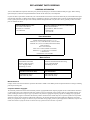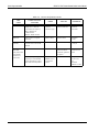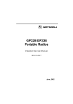
1
GTX/GTX LTR/
LTS 2000™
Portable Radios
Service Manual
*6802945C75-A*
68P02945C75-A
Motorola Inc.
8000 West Sunrise Boulevard
Fort Lauderdale, Florida 33322-9934
SAFE AND EFFICIENT OPERATION OF TWO-WAY RADIOS
SCOPE
This document provides information and instructions for the safe and efficient operation of Motorola Portable two-way Radios.
The information provided in this document supersedes the general safety information contained in user guides published prior to 1st January 1998.
For information regarding radio use in a hazardous atmosphere please refer to the Factory Mutual (FM) Approval Manual Supplement or Instruction Card,
which is included with radio models that offer this capability.
EXPOSURE TO RADIO FREQUENCY ENERGY
National and International Standards and Guidelines
Your Motorola two-way Radio, which generates and radiates radio frequency (RF) electromagnetic energy (EME) is designed to comply with the following
national and international standards and guidelines regarding exposure of human beings to radio frequency electromagnetic energy:
•
Federal Communications CommissionReport and Order No. FCC 96-326 (August 1996)
•
American National Standards Institute (C95-1-1992)
•
National Council on Radiation Protection and Measurements (NCRP - 1986)
•
International Commission on Non-Ionizing Radiation Protection (ICNRP - 1986)
•
European Committee for Electrotechnical Standardization (CENELEC)
-
Env. 50166 - 1 1995E - Human Exposure to Electromagnetic Fields Low Frequency (0 Hz to 10kHz)
-
Env. 50166 - 2 1995E - Human Exposure to Electromagnetic Fields High Frequency (10kHz to 300Ghz)
-
Proceedings of SC211/8 1996 - Safety Considerations for Human Exposure to E.M.Fs from Mobile Telecommunications Equipment (M.T.E.) in the
Frequency Range 30MHz - 6GHz (E.M.F - Electromagnetic Fields)
To assure optimal radio performance and that human exposure to radio frequency electromagnetic energy is within the guidelines set forth in the above
standards, always adhere to the following procedures:
Portable Radio Operation and EME Exposure
•
When transmitting with a portable radio, hold the radio in a vertical position with its microphone 1 to 2 inches (2.5 to 5.0 centimeters) away
from your mouth. Keep antenna at least 1 inch (2.5 centimeters) from your head and body.
•
If you wear a portable two-way radio on your body, ensure that the antenna is at least 1 inch (2.5 centimeters) from your body when transmitting.
ELECTROMAGNETIC INTERFERENCE/COMPATIBILITY
NOTE: Nearly every electronic device is susceptible to electromagnetic interference (EMI) if inadequately shielded, designed or otherwise configured for
electromagnetic compatibility.
•
To avoid electromagnetic interference and/or compatibility conflicts, turn off your radio in any facility where posted notices instruct you to do so. Hospitals or health care facilities may be using equipment that is sensitive to external RF energy.
•
When instructed to do so, turn off your radio when on board an aircraft. Any use of a radio must be in accordance with airline regulations or crew instructions.
!
OPERATIONAL WARNINGS
•
FOR VEHICLES WITH AN AIR BAG
Do not place a portable radio in the area over an air bag or in the air bag deployment area. Air bags inflate with great force. If a portable radio is
placed in the air bag deployment area and the air bag inflates, the radio may be propelled with great force and cause serious injury to occupants of
the vehicle.
•
POTENTIALLY EXPLOSIVE ATMOSPHERES
Turn off your two-way radio when you are in any area with a potentially explosive atmosphere, unless it is a radio type especially qualified for use
in such areas (for example, Factory Mutual Approved). Sparks in a potentially explosive atmosphere can cause an explosion or fire resulting in
bodily injury or even death.
•
BATTERIES
Do not replace or charge batteries in a potentially explosive atmosphere. Contact sparking may occur while installing or removing batteries and
cause an explosion.
•
BLASTING CAPS AND AREAS
To avoid possible interference with blasting operations, turn off your radio when you are near electrical blasting caps, in a blasting area, or in areas
posted: “Turn off two-way radio”. Obey all signs and instructions.
NOTE: The areas with potentially explosive atmospheres referred to above include fueling areas such as: below decks on boats; fuel or chemical
transfer or storage facilities; areas where the air contains chemical or particles, such as grain, dust or metal powders; and any other area where you
would normally be advised to turn off your vehicle engine. Areas with potentially explosive atmospheres are often but not always posted.
!
OPERATIONAL CAUTIONS
•
DAMAGED ANTENNAS
Do not use any portable two-way radio that has a damaged antenna. If a damaged antenna comes into contact with your skin, a minor burn can
result.
•
BATTERIES
All batteries can cause property damage and/or bodily injury such as burns if a conductive material such as jewelry, keys, or beaded chains touch
exposed terminals. The conductive material may complete an electrical circuit (short circuit) and become quite hot. Exercise care in handling any
charged battery, particularly when placing it inside a pocket, purse, or other container with metal objects.
REPLACEMENT PARTS ORDERING
ORDERING INFORMATION
You can order additional components and some piece parts directly through your GTX/GTX LTR/LTS 2000 price pages. When ordering
replacement parts, include the complete identification number for all chassis, kits, and components.
If you do not know a part number, include with your order the number of the chassis or kit which contains the part, and a detailed description
of the desired component. If a Motorola part number is identified on a parts list, you should be able to order the part through Motorola Parts.
If only a generic part is listed, the part is not normally available through Motorola. If no parts list is shown, generally, no user serviceable
parts are available for the kit.
Motorola Radio Support Center
3761 South Central Avenue
Rockford, IL 61102-4294
1-815-489-1000
Motorola United States Federal Government Depot
7940 Penn Randall Place
Upper Marlboro, MD 20772-2627
1-800-969-6680
1-301-736-4300
Parts Information
7:30 A. M. to 7:00 P. M. (Central Standard Time)
Monday through Friday (Chicago, U. S. A.)
Domestic (U. S. A.): 1-800-422-4210, or 847-538-8023
1-800-826-1913, or 410-712-6200 (Federal Government)
TELEX: 280127
FAX: 1-847-538-8198
FAX: 1-40-712-4991 (Federal Government)
Domestic (U. S. A.) after hours or weekends:
1-800-927-4357
International: 1-847-538-8023
Motorola Parts
Accessories and Aftermarket Division
(United States and Canada)
Attention: Order Processing
1313 E. Algonquin Road
Schaumburg, IL 60196
Accessories and Aftermarket Division
Attention: International Order Processing
1313 E. Algonquin Road
Schaumburg, IL 60196
Customer Service/Order Entry
Parts Identification
1-800-422-4210 (Voice)
1-847-538-8198 (FAX)
1-847-538-0021 (Voice)
1-847-538-8194 (FAX)
Manual Revisions
Changes which occur after this manual is printed are described in “IMRs.” These IMRs provide complete information on changes including
pertinent parts listing data.
Computer Software Copyrights
The Motorola products described in this manual may include copyrighted Motorola computer programs stored in semiconductor memories
or other media. Laws in the United States and other countries preserve for Motorola certain exclusive rights for copyrighted computer programs, including the exclusive right to copy or reproduce in any form the copyrighted computer program. Accordingly, any copyrighted
Motorola computer programs contained in the Motorola products described in this manual may not be copied or reproduced in any manner
without the express written permission of Motorola. Furthermore, the purchase of Motorola products shall not be deemed to grant either
directly or by implication, estoppel, or otherwise, any license under the copyrights, patents or patent applications of Motorola, except for the
normal non-exclusive royalty free license to use that arises by operation of law in the sale of a product.
Table of Contents
Table of Contents........................................................................................................................................ i
Safe and Efficient Operation of Two-way Radios............................................................ Inside front cover
GTX/GTX LTR Portable Radio Model Chart........................................................................................................................ v
LTS 2000/LTS 2000 SmartZone and SmartNet Plus Portable Radios Model Chart...................................................... vi
GTX/GTX LTR/LTS 2000 Options...................................................................................................................................... vii
GTX/GTX LTR/LTS 2000 Accessories .............................................................................................................................. viii
Performance Specifications...................................................................................................................................................... x
Service Aids............................................................................................................................................................................... xi
Test Equipment......................................................................................................................................................................... xi
Service Tools ............................................................................................................................................................................ xii
Test Set Service Cable .................................................................................................................................................... xiii
Radio Model Numbering System ....................................................................................................................................... xiv
Radio Service Software Information..................................................................................................................................... xv
Configuring the RIB and Radio............................................................................................................................................. xv
Notes: ...................................................................................................................................................................................... xvi
Important Safety Information: Intrinsically Safe Radios................................................................................................ xvii
FMRC Approved Equipment ...................................................................................................................................... xvii
Repair of FMRC Approved Products........................................................................................................................ xviii
Repair ............................................................................................................................................................................. xviii
Relabeling ......................................................................................................................................................................... xix
Do Not Substitute Options or Accessories .................................................................................................................. xix
Vehicles Equipped with Air Bags ........................................................................................................................................ xix
Section 1
Radio Disassembly/Assembly
Overview ................................................................................................................................................................................. 1-1
Safety Information.................................................................................................................................................................. 1-1
Radio Disassembly................................................................................................................................................................. 1-1
Battery Removal .............................................................................................................................................................. 1-1
Chassis Removal.............................................................................................................................................................. 1-1
Main Board Removal ...................................................................................................................................................... 1-2
Front Housing Board Removal ..................................................................................................................................... 1-3
Radio Reassembly .................................................................................................................................................................. 1-3
Front Housing Reassembly............................................................................................................................................ 1-3
Front Housing Reassembly Ñ Basic Model ................................................................................................................ 1-4
Chassis Reassembly ........................................................................................................................................................ 1-4
Radio Reassembly ........................................................................................................................................................... 1-5
Section 2
Theory of Operation
Overview ................................................................................................................................................................................. 2-1
Receiver.................................................................................................................................................................................... 2-1
Intermediate Frequency (IF) .......................................................................................................................................... 2-1
Transmitter.............................................................................................................................................................................. 2-1
Frequency Generation Unit .................................................................................................................................................. 2-4
©Motorola Inc., 1998
All Rights Reserved
68P02945C75-A
i
Table of Contents
GTX/GTX LTR /LTS 2000 Portable Radios Service Manual
Controller................................................................................................................................................................................ 2-5
Functions.......................................................................................................................................................................... 2-5
Normal Operation .......................................................................................................................................................... 2-5
Clock Synthesizer ........................................................................................................................................................... 2-5
Bus Operation.................................................................................................................................................................. 2-5
RAM .................................................................................................................................................................................. 2-5
EEPROM .......................................................................................................................................................................... 2-5
SPI Interface..................................................................................................................................................................... 2-6
LED Control..................................................................................................................................................................... 2-6
Audio & Data Circuitry ................................................................................................................................................. 2-6
External PTT Sense Circuits .......................................................................................................................................... 2-6
MIC Amplifier................................................................................................................................................................. 2-6
TX Data Circuits.............................................................................................................................................................. 2-6
Sub-Audible Data (PL/DPL) ........................................................................................................................................ 2-7
High-Speed Data............................................................................................................................................................. 2-7
DTMF Data ...................................................................................................................................................................... 2-7
MDC Data ........................................................................................................................................................................ 2-7
RX Audio Processing and Digital Volume Control ................................................................................................... 2-7
Audio Power Amplifier ................................................................................................................................................. 2-8
Audio PA Muting and Output Protection .................................................................................................................. 2-8
Receive Data Circuits ..................................................................................................................................................... 2-8
Alert Tone Circuits ......................................................................................................................................................... 2-8
Section 3
Accessory
Overview.................................................................................................................................................................................
Description .............................................................................................................................................................................
Operation ................................................................................................................................................................................
Handling Precautions ...........................................................................................................................................................
Maintenance ...........................................................................................................................................................................
3-1
3-1
3-1
3-1
3-2
Section 4
Troubleshooting
Overview................................................................................................................................................................................. 4-1
Troubleshooting Charts ........................................................................................................................................................ 4-1
Troubleshooting Flow Chart for Receiver ........................................................................................
Troubleshooting Flow Chart for Transmitter....................................................................................
Troubleshooting Flow Chart for Synthesizer....................................................................................
Troubleshooting Flow Chart for Controller ......................................................................................
4-2
4-3
4-4
4-5
Section 5
Radio Diagnostic Utilities
Test Mode/Entry ...................................................................................................................................................................
Test Mode/Channel Selection .............................................................................................................................................
Test Mode/Tx Modulation...................................................................................................................................................
Exiting Test Mode..................................................................................................................................................................
Fail Mode ................................................................................................................................................................................
Performance Checks..............................................................................................................................................................
5-1
5-1
5-2
5-2
5-2
5-3
Section 6
Maintenance
Introduction............................................................................................................................................................................ 6-1
ii
68P02945C75-A
June 1999
GTX/GTX LTR /LTS 2000 Portable Radios Service Manual
Preventive Maintenance........................................................................................................................................................ 6-1
Inspection ......................................................................................................................................................................... 6-1
Cleaning............................................................................................................................................................................ 6-1
Safe Handling of CMOS Devices ......................................................................................................................................... 6-1
Repair Procedures and Techniques ..................................................................................................................................... 6-2
General.............................................................................................................................................................................. 6-2
Over-Molded Pad-Array Carrier (OMPAC) ............................................................................................................... 6-3
Section 7
Radio Tuning Procedure
Radio Tuning Procedure ....................................................................................................................................................... 7-1
General.............................................................................................................................................................................. 7-1
Tuning Procedure................................................................................................................................................................... 7-2
Reference Oscillator Alignment .................................................................................................................................... 7-2
Squelch.............................................................................................................................................................................. 7-2
RSSI (Received Signal Strength Indicator)................................................................................................................... 7-3
Transmitter Power .......................................................................................................................................................... 7-3
Transmit Deviation Balance (Compensation) & Deviation Limit ............................................................................ 7-3
Transmit Deviation Limit............................................................................................................................................... 7-3
Section 8
Schematic Diagrams, Circuit Board Details, and Parts Lists
Schematic Diagram for FUF5590A/FUF5591A RF Board Wiring Diagram......................................... 8-2
Schematic Diagram for FUF5590A/FUF5591A RF Board Receiver Module ....................................... 8-3
Schematic Diagram for FUF5590A/FUF5591A RF Board, Synthesizer Module.................................. 8-4
Schematic Diagram for FUF5590A/FUF5591A RF Board, Transmitter Module.................................. 8-5
Circuit Board Details for FUF5590A/FUF5591A, RF Board ................................................................ 8-6
Parts Lists for FUF5590A RF Board ...................................................................................................... 8-7
Parts Lists for FUF5591A RF Board .................................................................................................... 8-10
Circuit Board Details, Schematic Diagram, & Parts List for FLN8517A Battery Filter Board ........... 8-11
Parts Lists for FLN8517A Battery Filter Board ................................................................................... 8-11
Circuit Board Details for FLN8514A , F LN9053A, FLN9064A, HLN9859, HLN9860, FEN1648, and
FEN1656 Logic Board.......................................................................................................................... 8-12
Schematic Diagram for FLN8514A, FLN9053A, FLN9064A, HLN9859, HLN9860, FEN1648, and
FEN1656 Logic Board.......................................................................................................................... 8-13
Parts Lists for FLN8514A Logic Board................................................................................................ 8-14
Parts Lists for FLN9053A Logic Board................................................................................................ 8-14
Parts Lists for FLN9064A Logic Board................................................................................................ 8-14
GTX/GTX LTR Mechanical Parts List................................................................................................. 8-14
GTX Exploded View ............................................................................................................................ 8-14
GTX/GTX LTR Basic Model Mechanical Parts List ........................................................................... 8-14
GTX Basic Model Radio Exploded View ............................................................................................ 8-14
LTS 2000 Mechanical Parts List........................................................................................................... 8-15
LTS 2000 Exploded View .................................................................................................................... 8-16
Miscellaneous Parts Lists...................................................................................................................... 8-17
Parts Lists for FHN5873A Housing (GTX/GTX LTR) .................................................................. 8-17
Parts Lists for FHN5874A Housing (LTS 2000) ............................................................................ 8-17
Parts Lists for FHN5978A Housing (LTS 2000 SmartZone) ......................................................... 8-17
June 1999
68P02945C75-A
iii
Table of Contents
GTX/GTX LTR /LTS 2000 Portable Radios Service Manual
Miscellaneous Parts Lists (cont.) ..........................................................................................................
Parts Lists for FLN8574A Housing Miscellaneous Parts (GTX/GTX LTR) .................................
Parts Lists for FLN8576A Housing Miscellaneous Parts (LTS 2000) ...........................................
Parts Lists for FLN8575A Shield & Parts ......................................................................................
Parts Lists for FLN8577A Miscellaneous Parts (GTX/GTX LTR) ................................................
Parts Lists for FLN8665A Miscellaneous Parts (LTS 2000) ..........................................................
Parts Lists for FLN8665B Miscellaneous Parts (LTS 2000 SmartZone) .......................................
Parts Lists for FSN5509A Speaker & Microphone Assembly .......................................................
Parts Lists for NAF5037A Antenna................................................................................................
8-18
8-18
8-18
8-18
8-18
8-18
8-18
8-18
8-18
, Motorola, Private-Line, and Digital Private-Line are trademarks of Motorola, Inc.
IBM is a registered trademark, and PC DOS, PC XT/AT/Convertible and PS/2 Model 30/50/70 are trademarks of
International Business Machine Corporation.
MS-DOS is a trademark of Microsoft Corp.
iv
68P02945C75-A
June 1999
GTX/GTX LTR /LTS 2000 Portable Radios Service Manual
Foreword
GTX/GTX LTR Portable Radio Model Chart
GTX/GTX LTR Portable Radio Model Chart
GTX 800MHz Portable Radio Model Chart
Model
Description
H11UCC6DB1_N
GTX Basic Radio, 800MHz, Privacy Plus
H11UCC6DU1_N
GTX Basic Radio, 800MHz, LTR
H11UCD6CB1_N
GTX Keypad Radio, 800MHz, Privacy Plus
H11UCD6CU1_N
GTX Keypad Radio, 800MHz, LTR
Item
X
X
X
X
X
X
Description
HLN3140
Front Housing Assembly with Logic Board
HLN3141
Front Housing Assembly with Logic Board
FLN2392
Front Housing Assembly with Logic Board
X FLN2445
Front Housing Assembly with Logic Board
HLN9859
Logic Board & I/O Unit
HLN9860
Logic Board & I/O Unit
FEN1648
Logic Board & I/O Unit
X FEN1656
Logic Board & I/O Unit
X X X X FUF1191
2.5 ppm RF Unit
X X X X FLN2394
Chassis Assembly
x = Indicates one of each is required.
Not all kits on this page will be available from the Accessories and Aftermarket Division
June 1999
68P02945C75-A
v
Foreword
GTX/GTX LTR /LTS 2000 Portable Radios Service Manual
LTS 2000/SmartZone and SmartNet Plus Portable Radios Model Chart
LTS 2000/SmartZone and SmartNet Plus Portable Radios
Model Chart
Model
H10UCH6DC5AN
Description
LTS 2000 Portable Radio (For Existing Users Only)
H10UCH6DC5BN
LTS 2000 Portable Radio Q38 (SmartZoneª)
H10UCH6DC5BN
LTS 2000 Portable Radio Q37 (SMARTNET Plusª)
Item
X
X
X
X
Description
FLN2395A
Front Housing Assembly with Logic Board (for factory use only)
FLN2395B
Front Housing Assembly with Logic Board (for factory use only)
X FLN2550A
Front Housing Assembly with Logic Board (for factory use only)
FEN1649A
Logic Board & I/O Unit (Part of FLN2395A)
FEN1665A
Logic Board & I/O Unit (Part of FLN2395B)
X FEN1667A
Logic Board & I/O Unit (Part of FLN2550A)
X X X FUF1193A
1.5 ppm RF Unit
X X X FLN2394A
Chassis Assembly (Part of FUF1193A)
x = Indicates one of each is required.
Not all kits on this page will be available from the Accessories and Aftermarket Division
NOTE
Items with sufÞx may be upgraded in
the future.
vi
68P02945C75-A
June 1999
GTX/GTX LTR /LTS 2000 Portable Radios Service Manual
GTX/GTX LTR/LTS 2000 Options
GTX/GTX LTR/LTS 2000 Options
LTS 2000
GTX GTX/LTR
Model
GTX/GTX LTR/LTS 2000 Options
Option
Description
Factory Mutual (FM) Batteries
X
X
H236
Fully Approved Factory Mutual Intrinsically Safe Radio (includes FA 1200 mAH
battery)
X
X
H73
Factory Mutual Intrinsically Safe Radio (includes 600 mAH battery)
X
X
H224
600 mAH Slim Battery (deletes standard battery)
Antenna
X
X
H112
Omit Standard Antenna
Miscellaneous
X
X
H415
Bulk Packaging (minimum 10 units per line item)
Chargers
X
H951
Omit Standard Charger
X
H437
Add Rapid Rate Charger, 110 V
X
H438
Add Slow Rate Charger, 220 V
X
H439
Add Rapid Rate Charger, 220 V
June 1999
68P02945C75-A
vii
Foreword
GTX/GTX LTR /LTS 2000 Portable Radios Service Manual
GTX/GTX LTR/LTS 2000 Accessories
GTX/GTX LTR/LTS 2000 Accessories
LTS 2000
GTX/GTX LTR
Model
GTX/GTX LTR/LTS 2000 Accessories
Accessory
Description
Charger Pick-ups
X
HTN9803
Single Unit, Rapid Charger, UK Plug, 240 V
X
X
HTN9702
Single Unit Standard Charger, 110 V
X
X
HTN9042
Single Unit, Rapid Charger, 110 V
X
X
HTN9812
Multiple Unit, Rapid Charger, 220 V
X
X
HTN9719
Vehicular Charger, Adapter/Bracket. 12V for use with Single Unit Rapid Chargers
X
X
HTN9811
Multiple Unit, Rapid Chargers, European Plug, 220V
X
X
HTN9944
Wall Mounting Bracket for Multiple Unit Chargers
Antenna Pick-ups
X
X
NAF5042
806-941 MHz 1/4 Wavelength Whip
X
X
NAF5037
806-870 MHz 1/2 Wavelength Whip
X
X
HNN9628
1200 mAh High Capacity Battery
X
X
HNN9701
1200 mAh Fully Approved Factory Mutual Battery*
X
X
HNN8308
600 mAh Slimline Battery
X
X
HNN9808
600 mAh Fully Approved Factory Mutual Slim Battery*
X
X
HLN9421
DTMF Standard Leather Carry Case w/Swivel
X
X
HLN9426
DTMF Standard Leather Carry Case w/Swivel for Fully Approved FM 1200 mAH
X
X
HLN9427
DTMF Standard Leather Carry Case w/Swivel for Fully Approved FM 600 mAH
X
X
HLN9429
DTMF Standard Leather Carry Case w/Belt Loop for Fully Approved FM 1200 mAH
X
X
HLN9431
DTMF Standard Leather Carry Case w/Belt Loop for Fully Approved FM 600 mAH
X
X
HLN9076
Standard Molded Carry Holder with Belt Clip
X
X
HLN9149
Swivel Belt Loop Adapter for Use w/Carry Cases HLN9412, HLN9426, HLN9427
X
X
HLN9724
Belt Clip
X
X
TDN1022
Swivel - includes holster, belt and strap
X
HLN8255
Spring Belt Clip
NTN5243
Shoulder Strap (for use with all Carry Cases)
Battery Pick-ups
Carrying Accessories Pick-ups
X
X
Audio/RF Accessories:
X
X
HMN9030
Remote Speaker Microphone w/Coil Cord and Clip Back
X
X
HMN9727
Earpiece without Volume Control
X
X
HMN9752
Earpiece with Volume Control
X
HMN9754
2-Piece Surveillance Microphone, PTT and Microphone are combined in 1 Piece
X
X
BDN6720
Ear Receiver with /GP300 Style Connector
X
X
FLN8660
Audio Accessory Security Clamp
*These batteries are only compatible with portables ordered from the factory with the Factory Mutual option.
viii
68P02945C75-A
June 1999
GTX/GTX LTR /LTS 2000 Portable Radios Service Manual
Foreword
GTX/GTX LTR/LTS 2000 Accessories (cont.)
LTS 2000
GTX/GTX LTR
Model
GTX/GTX LTR/LTS 2000 Accessories
Documentation Kits
X
68P02946C80
GTX Portable Radio UserÕs Guide
X
68P02948C65
GTX LTR Portable Radio UserÕs Guide
68P02945C75
GTX/GTX LTR/LTS 2000 Portable Radios Service Manual
68P02945C85
LTS 2000 Portable Radio UserÕs Guide
X
X
X
Radio Service Software (RSS)*
X
RVN4150
GTX/GTX LTR
X
RVN4156
LTS 2000
X
68P02946C20
LCS/LTS 2000 RSS UserÕs Guide
68P02948C70
GTX/GTX LTR RSS UserÕs Guide
HKN9857
Programming/Test Cable
X
X
X
* See RSS information for hardware details.
Prices and availability subject to change without notice
June 1999
68P02945C75-A
ix
Foreword
GTX/GTX LTR /LTS 2000 Portable Radios Service Manual
Performance Specifications
Performance Specifications
GENERAL
RECEIVER
FCC Designation:
GTX /GTX LTR
LTS 2000:
AZ489FT5776
AZ489FT5777
Power Supply:
NiCad Battery
Battery Voltage:
Nominal:
Range:
7.5 V
6 to 9 V
Battery Drain, Typical:
Standby:
Receive:
Transmit:
65 mA
190 mA
1500 mA
Temperature Range:
Operating:
Storage:
-30+60ûC*
-40+85ûC
Dimensions (H x W x D)
GTX (total height includes
radio, antenna adaptor, and
antenna)
LTS 2000 (total height
includes radio, antenna
adaptor, and antenna)
TRANSMITTER
Frequency Range:
851-870 MHz
RF Power:
3W
Bandwidth
19 MHz
Frequency range:
806-825 MHz
851-870 MHz
Usable Sensitivity
(12 dB SINAD):
0.35 µV max.
Freq. Stability
(-30+60ûC; 25ûC ref.:)
(821-824 MHz Capable):
±0.00025%
±0.00015%
Intermodulation:
-65 dB
Emission
(Conducted and Radiated):
-48 dBc
FM Hum and Noise
(Companion Receiver):
-40 dB
Distortion;
5%
Modulation Limiting:
(821-824 MHz):
±5 kHz
±4 kHz
Recommended Battery:
High Capacity
HNN9628
NTN7143
Selectivity
(25 kHz Adjacent
Channel):
-65 dB
Spurious Rejection:
-65 dB
Freq. Stability:
(-30+60ûC; 25ûC ref.):
(821-824 MHz
Capable):
±0.00025%
±0.00015%
Rated Audio:
500 mW
Distortion (At Rated
Audio):
5%
Channel Spacing
25 kHz
12.86x2.32x1.09Ó
326.53 x59 x27.8 mm
12.86x2.32x1.17Ó
326.53x59x29.8 mm
Weight (w/Antenna):
GTX less Battery:
0.69 lbs (314 gr)
GTX + Standard Battery:
1.20 lbs (544 gr)
GTX + HNN9701 Battery
1.38 lbs (625 gr)
LTS 2000 less Battery:
0.68 lbs (310 gr)
LTS 2000 + Standard Battery:
1.19 lbs (540 gr)
LTS 2000 + HNN9701 Battery:
1.37 lbs (621 gr)
* Operating for Display: -20+60ûC
All speciÞcations subject to change without notice
x
68P02945C75-A
June 1999
GTX/GTX LTR /LTS 2000 Portable Radios Service Manual
Foreword
Service Aids
Service Aids
The following table lists service aids recommended for working on the GTX/GTX LTR/LTS 2000.
MOTOROLA NO.
DESCRIPTION
APPLICATION
RLN4008
Radio Interface Box
Enables communication between the radio and the
computerÕs serial communications adapter.
0180357A57 (120 Vac)
0180358A56 (220 Vac)
RIB Power Supply
Used to supply power to the RIB.
30-80369B72 for IBM PC ATs,
or 30-80369B71 for all other
IBM PCs
Computer Interface Cable
Connects the computerÕs serial communications adapter to
the RIB.
RLN4438
AT to XT Computer Adapter
Allows 30-80369B72 to plug into a XT style communications
port.
HKN9857
Programming / Test Cable
Connects radio to RIB. And can be used as a Battery
Eliminator.
RVN4150 for GTX
RVN4156 for LTS 2000
Radio Service Software
Software on 3-1/2 in.
RTX4005
Portable Test Set
Enables connection to the audio/accessory jack. Allows
switching for radio testing.
RKN4034
Test Set Cable
Connects radio to RTX4005B Test Box.
FLN8769
Tune and Test Fixture
Enables board level maintenance
5880348B33
SMA Female to BNC Female
Adapter
Enables RF connection to radio antenna connector.
Test Equipment
The following table lists test equipment required to service the GTX/GTX LTR/LTS 2000.
MOTOROLA NO.
DESCRIPTION
CHARACTERISTICS
Communications
System Analyzer
*R1049A
Digital Multimeter
*S1100A
Audio Oscillator
67 to 161.4Hz tones
Used with service monitor for injection of
PL tones
*S1053D, *SKN6009A,
*SKN6001A
AC Voltmeter, Power
Cable for meter, Test
leads for meter
1 mV to 300 V, 10-Megohm
input impedance
Audio voltage measurements
R1053
Dual-trace Oscilloscope
20 MHz bandwidth,
5 mV/cm - 20 V/cm
Waveform measurements
*S1350C, *ST1215B
(VHF) *ST1223B (UHF)
*T1013A
Wattmeter,
Plug-in Elements (VHF
& UHF), RF Dummy
Load
50-Ohm, + 5% accuracy
10 W, max. 0-1000 MHz,
300 W
Transmitter power output measurements
S1339A
RF Millivolt Meter
100 µV to 3 VRF, 10 KHz to
1.2 GHz
RF level measurements
*R1013A
SINAD Meter
S1347D or
S1348D (prog)
DC Power Supply
June 1999
This monitor will
substitute for items with
an asterisk *
APPLICATION
R2000, R2400, or
R2001D with trunking
option
Frequency/deviation meter and signal
generator for wide-range troubleshooting and alignment
Two meters recommended for AC/DC
voltage and current measurements
Receiver sensitivity
0-20 Vdc, 0-5 Amps
68P02945C75-A
Bench supply for 10Vdc
xi
Foreword
GTX/GTX LTR /LTS 2000 Portable Radios Service Manual
Service Tools
Service Tools
The following table lists the tools recommended for working on this family of radios; these tools are also available
from Motorola. Note that the R-1070A workstation requires the use of a specific Òheat focus headÓ for each of the
components on which this item is used. Each of these heat focus heads must be ordered separately. The individual
heat focus heads (and the components on which they are used) are listed at the end of the table.
MOTOROLA NO.
DESCRIPTION
APPLICATION
6680387A59
Extractor, 2-contact
6680387A64
Heat controller with safety stand, or
6680387A65
Safety stand only
0180381B45 110 Vac or
0180300E06 220 Vac
MBT250 Surface-mount/ thru-hole repair
station
Temperature-controlled, self-contained soldering/desoldering repair station for installation
and removal of surface-mounted devices.
8180369E97
Flux holder/applicator arrays for repair.
Allows for the proper amount of ßux to be
applied to pad grid.
1105139W02
30cc plastic syringe and ßux paste
For use with ßux holder/applicator
8180369E97.
0180386A81
Miniature digital readout soldering station
(incl. 1/64Ó micropoint tip)
0180386A78
Illuminated magnifying glass with lens attachment
0180386A82
Anti-static grounding kit
6684253C72
Straight prober
6680384A98
Brush
1010041A86
Solder (RMA type), 63/37, 0.020" diameter
1 lb. spool
1080370B43
RMA liquid ßux
R-1319A
Shields and surface-mounted component IC removal/rework station (order all heat
focus heads separately)
xii
Removal of discrete surface-mounted devices.
Used during all radio assembly and disassembly procedures.
68P02945C75-A
Removal of surface-mounted integrated circuits.
June 1999
GTX/GTX LTR /LTS 2000 Portable Radios Service Manual
Foreword
Service Tools
HEAT-FOCUS
HEADS
INSIDE DIMENSIONS
OF HEADS
6680334B52
0.572" x 0.572"
U701
6680371B15
0.460" x 0.560"
VCO shield SH260
USED ON
MAXIMUM PRESCRIBED
HEAT SETTING
Refer to Maintenance Section of Manual
for prescribed heat setting.
Test Set Service Cable
P1
6
12
3.5 mm plug
NOTE: Pins 2 and 7
are cut.
tip
sleeve
5
4
12
2
6
7
3
14
9
(P1) DETAIL
FRONT SIDE
Figure 1.
June 1999
sleeve
8
11
1
14 Speaker (Hi)
47 Ohm, 1/2W
+ 1.0 µF
9 Speaker (Lo)
11
2
3 Gnd
tip
2.5 mm plug
33K, 1/8 W
4
Mic. Audio
5
PTT
1
7
8
NOTE: For proper speaker impedance, the RTX4005B
test set Audio out switch must be set to the “MX” position
Service Cable (RKN4034A) for the Test Set (RTX4005B)
68P02945C75-A
xiii
Foreword
GTX/GTX LTR /LTS 2000 Portable Radios Service Manual
Radio Model Numbering System
Radio Model Numbering System
The model number, serial number, and Motorola FCC designation number are all on a label attached to the back of your radio.
All GTX/GTX LTR/LTS 2000 radio models are synthesized, 8-channel units that come standard with Tone Private-Line (TPL)/
Digital Private-Line (DPL) coded squelch or carrier squelch, which may be enabled/disabled on a per channel basis. Programming changes can be made by your local dealer.
GTX
Model Number:
H
1
1
U
C
D
6
C
B
1
A
N
Position:
1
2
3
4
5
6
7
8
9
10 11 12
Position 12 Unique Model Variations
Standard Package
Position 1 - Type of Unit
H = Hand-Held Portable
Position 2 & 3 - Model Series
Position 11- Version
Version Letter (Alpha) - Major Change
Position 4 - Frequency Band
806-870 MHz
Position 10 - Feature Level
Basic
Position 5 - Power Level
3W
Position 6 - Physical Package
Standard Control with Display
Position 9 - Primary System Type
Privacy Plus¨
Position 8 - Primary Operation
Trunked Twin Type
Position 7 - Channel Spacing
20/25 kHz
LTR
Model Number:
H
1
1
U
C
D
6
C
U
1
A
N
Position:
1
2
3
4
5
6
7
8
9
10 11 12
Position 12 Unique Model Variations
Standard Package
Position 1 - Type of Unit
H = Hand-Held Portable
Position 2 & 3 - Model Series
Position 11- Version
Version Letter (Alpha) - Major Change
Position 10 - Feature Level
Basic
Position 4 - Frequency Band
806-870 MHz
Position 5 - Power Level
3W
Position 6 - Physical Package
Standard Control with Display
Position 9 - LTR
Position 8 - Primary Operation
Trunked Twin Type
Position 7 - Channel Spacing
25 kHz
Model Number:
H
1
0
U
C
H
LTS 2000
6 D C
5
Position:
1
2
3
4
5
6
7
10 11 12
8
9
N
Position 12 Unique Model Variation
Standard Package
Position 1 - Type of Unit
H = Hand-Held Portable
Position 2 & 3 - Model Series
Position 11- Version
Version Letter (Alpha/Beta ) - Major Change
Position 10 - Feature Level
Standard Package
Position 4 - Frequency Band
806-870 MHz
Position 9 - Primary System Type
Clear SMARTNETª
Position 5 - Power Level
3W
Position 6 - Physical Package
Full Keypad with Display
Position 7 - Channel Spacing
20/25 kHz
xiv
A
Position 8 - Primary Operation
Dual Mode Trunked
68P02945C75-A
June 1999
GTX/GTX LTR /LTS 2000 Portable Radios Service Manual
Foreword
Radio Service Software Information
Radio Service Software Information
To run the Radio Service Software, you will need the following equipment:
Required Equipment:
IBM XT, AT, Convertible, or System/2 Model 30/50TM with 512K RAM, Dual Floppy Disk Drives or one
Floppy Disk and one Hard Disk.
PC DOSTM or MS-DOSTM 3.0 or later.
Radio Interface Box (RIB) RLN4008.
RIB to IBM AT cable 30-80369B72.
IBM AT cable to IBM XT computer adapter (optional) RLN4438.
Programming/Test cable.
RIB power supply 0180357A57 (120 Vac) or 0180358A56 (220 Vac).
1.
2.
3.
4.
5.
6.
7.
0180357A57 (120 Vac) or
0180358A56 (220 Vac)
RIB Power Supply.
Plugs into 120 or 220 Vac outlet.
30-80369B72 or
30-80369B71
RIB to Computer Cable.
Plugs into RIB and computer.
RSS
Manual
Computer
RVN4150D for GTX/GTX LTR or
RVN4156F for LTS 2000
Software
15 PIN
RLN4008
(RIB)
25 PIN
GTX/GTX LTR
LTS 2000 Radio
HKN9857
Programming / Test cable.
Connects between the RIB and radio.
Power Supply (7.5 Vdc)
Note: Battery can be used on
programming cable making
power supply optional.
Figure 2.
Equipment Setup
Configuring the RIB and Radio
1.
Connect the RIB to the computer (Figure 2).
2.
Plug the large 25-pin end of the HKN9857 programming cable into the RIB. The other end of this cable has
a Òbattery eliminator.Ó
3.
Slide the battery eliminator in place of the radioÕs battery.
4.
Plug power supply 0180357A57 (120 Vac) or 0180358A56 (220 Vac) into a wall outlet, and connect the other
end to the RIB.
5.
Connect the radio to a power supply and turn the volume control clockwise to turn it on.
June 1999
68P02945C75-A
xv
Foreword
GTX/GTX LTR /LTS 2000 Portable Radios Service Manual
Notes:
Notes:
xvi
68P02945C75-A
June 1999
GTX/GTX LTR/LTS 2000 Portable Radios Service Manual
Foreword
Important Safety Information: Intrinsically Safe Radios
Important Safety Information: Intrinsically Safe Radios
FMRC Approved Equipment
Anyone intending to use a radio in a location where hazardous concentrations of flammable material exist (hazardous atmosphere) is advised to become familiar with the subject of intrinsic safety and with the National Electric Code NFPA 70 (National
Fire Protection Association) Article 500 (hazardous [classified] locations).
An Approval Guide, issued by Factory Mutual Research Corporation (FMRC), lists manufacturers and the products approved
by FMRC for use in such locations. FMRC has also issued a voluntary approval standard for repair service (“Class Number
3605”).
FMRC Approval labels are attached to the radio to identify the unit as being FM Approved for specified hazardous atmospheres.
This label specifies the hazardous Class/Division/Group along with the part number of the battery that must be used. Their Approval mark is shown below.
!
WARNING
Do not operate radio communications equipment in a hazardous atmosphere
unless it is a type especially qualified (e.g. FMRC Approved) for such use. An
explosion or fire may result.
Do not operate the FMRC Approved Product in a hazardous atmosphere if it has
been physically damaged (e.g. cracked housing). An explosion or fire may result.
Do not replace or charge batteries in a hazardous atmosphere. Contact sparking
may occur while installing or removing batteries and cause an explosion or fire.
Do not replace or change accessories in a hazardous atmosphere. Contact sparking
may occur while installing or removing accessories and cause an explosion or fire.
Do not operate the FMRC Approved Product unit in a hazardous location with
the accessory contacts exposed. Keep the connector cover in place when
accessories are not used.
Turn radio off before removing or installing a battery or accessory.
Do not disassemble the FMRC Approved Product unit in any way that exposes the
internal electrical circuits of the unit.
Radios must ship from the Motorola manufacturing facility with the hazardous atmosphere capability and FM Approval labeling. Radios will not be “upgraded” to this capability and labeled in the field.
June 1999
68P02945C75-A
xvii
Foreword
GTX/GTX LTR/LTS 2000 Portable Radios Service Manual
Important Safety Information: Intrinsically Safe Radios
A modification changes the unit's hardware from its original design configuration. Modifications can only be done by the original product manufacturer at one of its FMRC audited manufacturing facilities.
!
WARNING
Failure to use an FMRC Approved Product unit with an FMRC Approved battery
or FMRC Approved accessories specifically approved for that product may result
in the dangerously unsafe condition of an unapproved radio combination being
used in a hazardous location.
Unauthorized or incorrect modification of an FMRC Approved Product unit will
negate the Approval rating of the product.
Repair of FMRC Approved Products
REPAIRS FOR MOTOROLA FMRC APPROVED PRODUCTS ARE THE RESPONSIBILITY OF THE USER.
You should not repair or relabel any Motorola manufactured communication equipment bearing the FMRC Approval label
(“FMRC Approved Product”) unless you are familiar with the current FMRC Approval Standard for repair service (“Class Number 3605”).
You may want to consider using a repair facility that operates under 3605 repair service approval.
!
WARNING
Incorrect repair or relabeling of any FMRC Approved Product unit could
adversely affect the Approval rating of the unit.
Use of a radio that is not intrinsically safe in a hazardous atmosphere could result
in serious injury or death.
FMRC's Approval Standard Class Number 3605 is subject to change at any time without notice to you, so you may want to
obtain a current copy of 3605 from FMRC. Per the December, 1994 publication of 3605, some key definitions and service requirements are as follows:
Repair
A repair constitutes something done internally to the unit that would bring it back to its original condition Approved by FMRC.
A repair should be done in an FMRC Approved facility.
Items not considered as repairs are those in which an action is performed on a unit which does not require the outer casing of
the unit to be opened in a manner which exposes the internal electrical circuits of the unit. You do not have to be an FMRC
Approved Repair Facility to perform these actions.
The radio support center is at the following address:
Motorola Radio Support Center
3761 South Central Avenue
Rockford, Ill, 61102
Telephone: (800) 227-6772
(815) 489-1000
xviii
68P02945C75-A
June 1999
GTX/GTX LTR/LTS 2000 Portable Radios Service Manual
Foreword
Vehicles Equipped with Air Bags
Relabeling
The repair facility shall have a method by which the replacement of FMRC Approval labels are controlled to ensure that any
relabeling is limited to units that were originally shipped from the Manufacturer with an FM Approval label in place. FMRC
Approval labels shall not be stocked by the repair facility. An FMRC Approval label shall be ordered from the original manufacturer as needed to repair a specific unit. Replacement labels may be obtained and applied by the repair facility providing
satisfactory evidence that the unit being relabeled was originally an FMRC Approved unit. Verification may include, but is not
limited to: a unit with a damaged Approval label, a unit with a defective housing displaying an Approval label, or a customer
invoice indicating the serial number of the unit and purchase of an FMRC Approved model.
Do Not Substitute Options or Accessories
The communications equipment package that Motorola submits to FMRC for testing and approval is tested as a system that
consists of the communications unit itself and the battery, antenna and other options or accessories that make up the rest of the
package to be approved. This approved package must be strictly observed and there must be no substitution of items, even if the
substitute you wanted to consider appears as an approved accessory elsewhere in the Guide for some other communications
equipment unit. Approved configurations are listed by FMRC Approved Product in the annual Approval Guide published by
FMRC. That guide, and the Approval Standard Class Number 3605 document, can be ordered from the following address.
Training Resource Center, Publications-Order Processing Dept.
Factory Mutual Engineering and Research
1151 Boston-Providence Turnpike
PO Box 9102
Norwood, MA, 02062
Telephone: (617) 762-4300
Vehicles Equipped with Air Bags
When planning the installation of communication equipment in a vehicle with one or more air bags, proceed as follows:
!
WARNING
Vehicles equipped with air bags.
An air bag inflates with great force. DO NOT place objects, including
communication equipment, in the area over the air bag or in the air bag
deployment area. If the communication equipment is improperly installed and
the air bag inflates, this could cause serious injury.
¥
Installation of vehicle equipment should be performed by a professional installer/technician qualiÞed in the
requirements for such installations. An air bagÕs size, shape and deployment area can vary by vehicle make,
model and front compartment conÞguration (e.g., bench seat vs. bucket seats).
¥
Contact the vehicle manufacturerÕs corporate headquarters, if necessary, for speciÞc air bag information for the
vehicle make, model and front compartment conÞguration involved in your communication equipment installation.
June 1999
68P02945C75-A
xix
Foreword
GTX/GTX LTR/LTS 2000 Portable Radios Service Manual
This page intentionally left blank
xx
68P02945C75-A
June 1999
Section 1
Radio Disassembly/Assembly
Overview
Radio Disassembly
This section explains, step by step, how to disassemble
and reassemble the GTX /GTX LTR/LTS 2000 radio.
Battery Removal
1.
Safety Information
The battery latch is located at the bottom of the
radio (Figure 1-1). Press and hold the battery
latch towards the front of the radio.
When testing and repairing the GTX/GTX LTR/LTS
2000 radio, observe the handling precautions to prevent unnecessary damage to the radio.
¥ Minimize handling of static-sensitive components and modules.
¥ Transport and store static-sensitive components
or assemblies in their original containers on a
metal rail. Label any package that contains
static-sensitive components or assemblies.
Figure 1-1.
2.
Press the battery housing against the radio,
while sliding the battery housing down until it
is free of the chassis rails (Figure 1-2).
800
¥ Discharge static electricity from the body by
wearing a grounded antistatic wrist strap while
handling these components. Servicing
static-sensitive components or assemblies
should only be done at a static-free work station
by qualiÞed service technicians. Increasing the
humidity in the work area minimizes static electricity problems.
Press Battery Latch
Battery
housing
¥ Do not allow anything that can generate or hold
a static charge on the workstation surface.
¥ Keep the component leads shorted together
whenever possible.
¥ Pick up components by their bodies. Never pick
them up by their leads.
¥ Do not slide the components over any surface.
¥ Avoid handling components in areas with a
ßoor or work surface covering that can generate
a static charge.
Figure 1-2.
3.
¥ Use a soldering iron connected to earth ground.
¥ Use only approved, anti-static, vacuum-type
desoldering tools for removing components.
To remove the battery, pull it straight out and
away from the radio.
Chassis Removal
1.
June 1999
Slide Battery Housing
68P02945C75-A
Pull the control knobs straight off.
1-1
Radio Disassembly/Assembly
GTX/GTX LTR/LTS 2000 Portable Radios Service Manual
Radio Disassembly
2.
Unscrew the antenna counter-clockwise until
it is detached from the radio.
3.
Carefully pry the chassis up on both sides,
near the bottom, with a ßat blade screwdriver
(Figure 1-3).
Figure 1-3.
4.
6.
Pull the chassis out and away from the
housing as shown by the arrow (Figure 1-4)
and beware of the front cover ßexible circuit.
7.
Remove the ßexible circuit using a ßat-blade
screwdriver or manually unlatching the ZIF
connector (Figure 1-5).
Remove Chassis
Figure 1-5.
Unlatching Zif Connector
Lift the chassis approximately halfway out.
Main Board Removal
IMPORTANT
You must disconnect the ribbon cable
before completely removing the chassis.
5.
The front shield holds the main board onto the chassis.
To remove the front shield:
Remove the ribbon cable connector from the
main board using pliers or a ßat blade
screwdriver (Figure 1-4).
1.
Place radio, chassis side down, on a ßat
surface.
2.
Apply downward pressure to chassis directly
above one of the clips opposite PTT switch.
3.
With a ßat blade screwdriver, carefully move
clip away from tab on chassis to release.
NOTE
Remove both clips opposite the PTT
switch Þrst, to ease remaining clip
removal.
Front Cover
Flexible Circuit
Figure 1-4.
1-2
4.
Repeat steps 2 and 3 for the remaining three
clips.
5.
Separate the main board from the chassis
(Figure 1-6).
Remove Ribbon Cable Connector
68P02945C75-A
June 1999
GTX/GTX LTR/LTS 2000 Portable Radios Service Manual
Radio Disassembly/Assembly
Radio Reassembly
Chassis
Gasket
Main board
Figure 1-8.
Locking clips
3.
Remove Front Housing Shield
Separate the front housing board from the
front housing.
Shield
Figure 1-6.
Separate Main Board From Chassis
Radio Reassembly
6.
Separate the ßexible circuit tail by undoing the
ZIF connector latch (Figure 1-7).
Figure 1-7.
Front Housing Reassembly
1.
Place the front housing on a cushioned ßat
surface with the front facing down.
2.
Place the keypad into the front housing
(Figure 1-9).
3.
Place the board on the keypad in the housing
(Figure 1-9).
Separate Flexible Circuit Tail
Front Housing Board Removal
1.
Place the front housing assembly with the
front facing down on a padded ßat surface.
This is to avoid the lens from being scratched.
2.
Remove the front housing shield using
tweezers or sharp end screwdriver by undoing
the four side catches (Figure 1-8).
June 1999
Figure 1-9.
68P02945C75-A
Place Keypad Into Front Housing
1-3
Radio Disassembly/Assembly
GTX/GTX LTR/LTS 2000 Portable Radios Service Manual
Radio Reassembly
4.
Fold the LCD ßexible circuit (Figure 1-11).
Make sure the LCD ßexible circuit is outside.
5.
Place the front housing shield into the front
housing using the four slots on the front
housing wall as the guide (Figure 1-10).
Figure 1-10.
Place Front Housing Shield
Into Front Housing
6.
Press down the shield at the four tabs until
tabs lock into the front housing catches.
7.
Slide in the lightpipe (Figure 1-11).
3.
Place the front housing shield into the front
housing using the four slots on the front
housing wall as the guide (see the following
Þgure).
4.
Press down the shield at the four tabs until
tabs lock into the front housing catches.
LCD flexible
circuit
Figure 1-11.
Chassis Reassembly
Slide In The Lightpipe
Front Housing Reassembly — Basic Model
1.
2.
1-4
Place the front housing on a cushioned ßat
surface with the front facing down.
Place the board in the housing (see the
following Þgure).
68P02945C75-A
1.
Place chassis on a ßat surface with the battery
rails downward.
2.
Insert the ßexible circuit tail end (marked ÒRFÓ
into the ZIF connector on the RF board and
lock the connector by engaging the latch
(Figure 1-12).
3.
Insert main board into chassis using alignment
pins as a guide (Figure 1-12).
4.
Place front shield on main board using tabs as
a guide (Figure 1-12).
June 1999
GTX/GTX LTR/LTS 2000 Portable Radios Service Manual
Radio Disassembly/Assembly
Radio Reassembly
Figure 1-14.
8.
Figure 1-12.
Replace Gasket
Place the chassis assembly and front housing
assembly on a ßat surface with the top face of
housing in a reverse and opposite direction
(Figure 1-15).
Align Pins
5.
Press down on front shield until chassis, main
board, and front shield are seated tightly
together.
6.
Hook locking clips Þrst to the chassis tab, then
push clips over on shield with thumb until
clips lock into front shield holes (Figure 1-13).
Figure 1-15.
Place Chassis Opposite of
Front Housing
Radio Reassembly
1.
Figure 1-13.
7.
June 1999
Insert the ßexible circuit tail from chassis to
ZIF connector on front housing board. Lock
the tail in the ZIF connector by pressing down
the latch.
Reinsert Locking Clips
NOTE
Flexible circuit tail must be fully inserted
to prevent short circuiting.
Replace chassis gasket (Figure 1-14).
68P02945C75-A
1-5
Radio Disassembly/Assembly
GTX/GTX LTR/LTS 2000 Portable Radios Service Manual
Radio Reassembly
NOTE
The gasket helps keep the radio free from
unwanted dirt, dust, and water. We recommend using a new lubricated gasket
(part no. 3280545C01) when reassembling the radio. Using an old gasket
could impair the overall seal quality of
the radio.
2.
Insert assembled chassis, main board, and
front shield into radio housing at
approximately a 45-degree angle (Figure 1-16).
Exercise caution while inserting the volume
and frequency controls through the housing
top.
Make certain that the
flexible circuit is completely
inside the housing.
IMPORTANT
The main board must be inserted into
chassis (Step 3) before you can secure
chassis into radio housing.
1-6
Figure 1-16.
3.
Connect microphone/speaker ribbon cable.
4.
While pressing chassis toward the housing
top, press the bottom end down into the
housing until the bottom housing wall snaps
over the chassis retaining studs.
68P02945C75-A
Insert Chassis into Housing
NOTE
The chassis should snap Þrmly into place
and the ßexible circuit should be placed
nicely inside the radio.
5.
Replace the knobs, antenna and battery.
June 1999
Section 2
Theory of Operation
Overview
Intermediate Frequency (IF)
This section provides a detailed theory of operation for
the GTX/GTX LTR/LTS 2000 and its components: the
receiver, transmitter, frequency generation circuitry,
controller and audio & data circuitry.
The Intermediate Frequency (IF) section of the portable
radio consists of several sections including the high IF,
the second LO, the second IF, and the IF IC chip. The
Þrst LO signal and the RF signal mix to the IF frequency of 45.1 MHz, and then enters the IF portion of
the radio.
Receiver
The receiver of the GTX/GTX LTR/LTS 2000 radios
consists of 4 major blocks: the front-end module, double balanced mixer, 45.1 MHz IF and back-end IF IC.
The GTX/GTX LTR/LTS 2000 front-end modules consist of three blocks of circuitry: a ceramic pre-selector
Þlter, RF ampliÞer and ceramic post-selector Þlter.
The ceramic pre- and post-selector Þlters are 3-pole,
bandpass Þlters. This topology maximizes the attenuation at the worst case image frequency for this receiver,
which is 90.2 MHz below the Þlter passband. The 3 dB
bandwidth is approximately 22 MHz, centered at
861 MHz. The center of the band insertion loss is
approximately 2 dB. The 3-pole Þlters are designed to
operate with a 50 Ohm input and output termination.
The RF ampliÞer, Q1, is a Motorola MRF9411 NPN
device biased in a common emitter conÞguration. The
amp is stabilized by the shunt feedback coil L2, and has
approximately 15 dB of gain with a noise Þgure of
about 2 dB. The ampliÞer draws 6.5 mA of current and
is supplied by the receiver 5 V supply (indicated as
Ò5RÓ on the schematics and block diagrams).
Terminating the RF ampliÞer is the post-selector Þlter.
This Þlter is the same as the pre-Þlter.
The net gain of the receiver front-end module is about
12 dB in the center of the band and about 11.5 dB at the
band edges. The net center of the band noise Þgure is
approximately 4.5 dB.
The receiver mixer is a double-balanced mixer which
provides excellent protection against receiver spurs
due to non-linearities, such as IM and half-IF. The
received signal mixes down to the frequency of the Þrst
IF, 45.1 MHz, and enters the IF circuitry. The mixer
operates with a LO level of +3 dBm and conversion loss
is about 7 dB.
June 1999
The signal Þrst enters the high IF, passes through a
crystal Þlter, is then ampliÞed by the IF amp, and then
passed through a second crystal Þlter. The Þrst crystal
Þlter provides selectivity, second image protection, and
intermodulation protection. The ampliÞer provides
approximately 16 dB of gain to the signal. The signal
then passes through the second crystal Þlter which provides further selectivity and second image protection.
The high IF has an approximate 3 dB bandwidth of
7 KHz.
The Þltered and ampliÞed IF signal then mixes with the
second local oscillator at 44.645 MHz. The second LO
uses an ampliÞer internal to the IF IC, an external crystal and some external chip parts. The oscillator presents an approximate level of -15 dBm to the second IF
mixer, internal to the IF IC.
The output of the mixing of the IF signal and the second LO produces a signal at 455 KHz (second IF). This
signal is then Þltered by external ceramic Þlters and
ampliÞed. It is then passed back to the IF IC, sent to a
phase-lock detector, and demodulated. The resulting
detected audio output is then sent to the ASFIC to
recover the audio.
Transmitter
The transmitter contains Þve basic circuits: a power
ampliÞer, an antenna switch, a harmonic Þlter, an
antenna matching network, and a power control. Refer
to the block diagram and the schematic for more information.
The power ampliÞer is an LD-MOS module. This module contains a 3-stage ampliÞcation with a supply voltage at 7.5 V. The LD-MOS is capable of supplying an
output power of 4.4 W with an input signal of 1 mW.
The power output can be varied by changing the biasing voltage at the Þrst stage.
68P02945C75-A
2-1
Theory of Operation
GTX/GTX LTR/LTS 2000 Portable Radios Service Manual
Transmitter
RF & AUDIO SECTION
VOLUME
VOL
ROTARY
SWITCH
& LEVEL
ENCODER
45.1 MHz
851-870 MHz
CONTROL
FRONT-END
MODULE
ROT1
2ND MIXER &
IF
1ST MIXER
DET_AUDIO
DEMODULATOR
ROT2
805.9-825 MHz
RX_INJ
SYNTHESIZER
16.8 MHz
ANTENNA
SWITCH
H FILTER
LOCK_DET
28-PIN
SYNT_EN
CONNECTOR
PEND_EN
TO LOGIC SECTION
2.1 MHz
TEMPUS
PENDULUM
MOD_IN
SPI_DATA
POWER
CONTROL
TXB+
PWR_REF
SPI_CLCK
TX_INJ
PREAMP
POWER
AMPLIFIER
806-825 MHz
TEMPUS_D/A
ACC.
CON.
AUDIO
PA
PWR_REF
RX_AUDIO
RED SCB4
YELLOW
MUTE
SCB3
D/A
DAC_SEL
5R SCB2
INT. SPKR
PEND_EN SCB1
MIC_EN
ACC.
CON.
MIC.
PREAMP
MIC_IN
INT. MIC
LOGIC SECTION:FOR FUF1190, FUF 1192, FUF1492A, FUF1493A, FUF1198
2.1 MHz
MOD_IN
RX_AUDIO
28-PIN
DET_AUDIO
CONNECTOR
MIC_IN
FROM RF SECTION
8-DIGIT
LCD DISPLAY
4 X 4 KEYPAD
SERIAL
EEPROM 4K
ASFIC
DISPLAY/KEYBOARD DRIVER
SPI BUS
PTT
MONITOR
OPT
LOCK_DET
SYNT_EN
PEND_EN
SCI
ROT1
ROT2
VOL_SENSE
DAC_SEL
µPROCESSOR
HC11K1
PARALLEL BUS
ROM 128K
RAM 8K
RADIO FUNCTIONAL BLOCK DIAGRAM
2-2
68P02945C75-A
June 1999
GTX/GTX LTR/LTS 2000 Portable Radios Service Manual
Transmitter
Ò5RÓ (5 V)
MIXER
RX IN
1ST
BANDPASS
FILTER
2ND
BANDPASS
FILTER
RF
AMP
LO +3 dBm
1ST
CRYSTAL
FILTER
2ND
CRYSTAL
FILTER
IF
AMP
DETECTED AUDIO
IF IC
RECEIVER BLOCK DIAGRAM
TXB+
0 dBm
FROM
VCO BUFFER
POWER
MODULE
RX IN
ANTENNA
SWITCH
COUPLER
HARMONIC
FILTER
ANTENNA
MATCHING
Vcontrol
POWER
CONTROL
RECTIFIER
POWER CONTROL REFERENCE
FROM DAC
TRANSMITTER BLOCK DIAGRAM
LOGIC SECTION FOR FUF1492B AND FUF 1493B
2.1 MHz
MOD_IN
8-DIGIT
LCD DISPLAY
4 X 4 KEYPAD
RX_AUDIO
SERIAL
EEPROM 4K
ASFIC
DET_AUDIO
28-PIN
CONNECTOR
MIC_IN
DISPLAY/KEYBOARD DRIVER
SPI BUS
FROM RF SECTION
LOW-BAT
PTT
MONITOR
OPT
LOCK_DET
SYNT_EN
PEND_EN
SCI
ROT1
ROT2
VOL_SENSE
DAC_SEL
µPROCESSOR
HC11K1
PARALLEL BUS
ROM 128K
June 1999
RAM 8K
68P02945C75-A
2-3
Theory of Operation
GTX/GTX LTR/LTS 2000 Portable Radios Service Manual
Frequency Generation Unit
The antenna switch circuit consists of two PIN diodes
(CR161 and CR162), a pi network (C126, L161, and part
of C162), and one current limiting resistor (R163). In
the transmit mode, TX B+ is applied to the circuit to
bias the diodes ÒonÓ. The shunt diode (CR161) shorts
out the receiver port, and the pi network, which operates as a quarter wave transmission line, transforms
the low impedance of the shunt diode to a high impedance at the input of the harmonic Þlter. In the receive
mode, the diodes are both off, and hence, there exists a
low attenuation path between the antenna and receiver
ports.
The voltage at the second input of the summing amp is
supplied by DAC U400-P9. This DAC is controlled by
the microprocessor and provides the reference voltage
for the control loop.
The error voltage at the input of U151B-13 produces a
voltage at its output which is in turn applied to the
drivers Q151, Q152. The voltage from Q151 collector is
applied to the controlled stage of the power module.
Frequency Generation Unit
The Frequency Generation Unit (FGU) consists of the
following major sections: the high stability reference
oscillator (U210), fractional-N synthesizer (U220), VCO
(U260), VCO buffer IC (U270) and Rx injection buffer
(Q280, Q281 and the surrounding components). The
VCO provides the carrier frequency for the transmitter
(U270 Tx output) and provides the local oscillator (LO)
injection signal for the Rx injection buffer (U270 Rx output). The phase-locked loop (PLL) circuit is provided
by the fractional-N synthesizer IC.
The harmonic Þlter consists of part of C121, C122 and
L121, C123, and C124. This Þlter attenuates the harmonic of the module to a level better than -55 dBc.
To optimize the performance of the transmitter and
receiver into an antenna, a network is used to match
the antennaÕs impedance to the harmonic Þlter. The
network is made up of C125 and L122.
The power control circuit consists of the networks
associated with U151, Q151, Q155, and U111.
The output of the VCO is ampliÞed by the prescaler
buffer, routed through a low-pass Þlter, and applied to
the prescaler dividers of the synthesizer. The divide
ratios are determined from information stored in memory and bussed to the synthesizer by way of the microcontroller. The divide ratio determines the VCO
frequency. The resulting VCO buffer signal is applied
to a comparator in the synthesizer. The synthesizer
comparator also receives a reference frequency by way
U111 is a directional coupler which detects the forward
power of the power module U101. The couple has 21
dB±1 dB coupling at port 2. The RF voltage at the coupler port 2 is rectiÞed by CR111, C111, R114, C112, and
is applied to U151A. This signal is ampliÞed by U151A
and applied to summing and integrator ampliÞer
U151B.
SWITCHING CCTS
FOR VCO AND BUFFER
POSITIVE MULTIPLIER
RX VCO
RX OUT
16.8 MHz
REF OSC
U210
RX INJ.
BUFFER
MIXER
RX BUFFER
LOOP
FILTER
REFERENCE
DIVIDER
TX OUT
MOD OUT
COUNTER FOR
MULTIPLIER
A/D
FRACTIONAL
DIVIDER
TX VCO
PRE-SCALER
DIVIDER
U260
VCO
U220
FRACTIONAL-N
SYNTHESIZER
MATCHING
CCT
RF PA
TX BUFFER
Prescaler
BUFFER
U270
VCO BUFFER IC
LOW PASS FILTER
2.1 MHz
REFERENCE
CLOCK TO
ASFIC
MODULATING
SIGNAL
FGU CIRCUITS
2-4
68P02945C75-A
June 1999
GTX/GTX LTR/LTS 2000 Portable Radios Service Manual
Controller
of reference divider input from the 16.8 MHz temperature-compensated reference oscillator. If the two frequencies differ, the synthesizer generates a control
(error) voltage causing the VCO to change frequency.
erating tones. Operations and operating conditions
within the radio are interpreted by the microprocessor
and fed back to the operator as visible (the display) or
audible (alert tone) indications of current status.
Modulation of the carrier is achieved by using a 2-port
modulation technique. The deviation of the low frequency tone, such as PL/DPL, is achieved by injecting
the signal into an analog/digital circuit in the synthesizer. The resulting digitized signal is then modulated
by the fractional N divider; this generates the required
deviation. The deviation of the high frequency tone is
achieved by modulating the modulation varactor on
the VCO. In order to cover a very wide bandwidth, the
VCO control voltage is stepped up by using a positive
multiplier circuit. A 13-V supply powers the phase
detector circuitry. The VCO signal is ampliÞed by the
integrated buffer ampliÞer of the VCO buffer. The
buffer IC Tx output signal is Þltered and channeled to
the RF PA (U101). The buffer IC Rx output signal is
connected to the Rx injection buffer. The output signal
of that buffer is supplied to the receiver Þrst mixer
(U50) as the injection signal.
Normal Operation
The regulated 5V output from U704 powers the microprocessor (U709) and the rest of the digital IC except
ASFIC (U701). The microprocessorÕs clock is generated
by the ASFIC, which has a built-in programmable clock
synthesizer.
Clock Synthesizer
Controller
Upon power-up and assuming that the ASFIC receives
a proper 2.1 MHz input on U701-P38 (which comes
from the transceiver board), the ASFIC outputs a
7.776 MHz CMOS square wave (0-5Vpp logic) on
U701-P30, which connects to the EXTAL input of the
microprocessor, U709-P73. The microprocessor operates at 1/4 of this frequency, which in this case computes to 1.944 MHz. In particular, the E clock output
(U709-P72) will be a 50% duty cycle square wave at this
frequency.
The GTX/GTX LTR/LTS 2000 controller is an open
architecture which consists of:
Bus Operation
¥ U709, Motorola 68HC11K1 microprocessor
¥ U701, Audio Signalling Filter Integrated Circuit,
ASFIC
¥ U703, EEPROM (4 Kbyte for GTX, 4 Kbyte or 8
Kbyte for LTS 2000)
¥ U705, 128/256 Kbyte OTP/FLASH ROM
¥ U706, 8/32 Kbyte Static RAM
¥ U707, LCD Display Driver
¥ U704, 5 V Voltage Regulator
U709, U703, U705, U706 and U707 are powered by
U704. U701 is powered from a 5V Regulator (U708) on
Radio Module. In addition to the external memory
devices, U709 has 768 bytes of RAM and 640 bytes of
EEPROM.
Functions
The microprocessor has two basic functions: interfacing with the outside world and controlling the internal
workings of the radio. The microprocessor interfaces
directly with the keypad, side buttons, PTT, rotary
switch, battery low indicator, EXT PTT and volume
sense. The microprocessor constantly monitors these
inputs and interprets any changes into commands that
control the rest of the radio. Some control functions it
performs include loading the synthesizer with the
desired RF frequency, turning the RF PA on or off,
enabling and disabling audio and data paths and gen-
June 1999
The microprocessor operates in expanded memory
mode and executes Þrmware contained in OTP/
FLASH ROM, U705. The microprocessor uses a nonmultiplexed address data bus, consisting data lines D0
through D7 and address lines A0-A17. In addition, the
microprocessor has integrated chip-select logic so that
external memories can be accessed without the need
for external address decoder gates. These chip-select
signals are provided by U709-P28 and P29.
When the controller board is functioning normally,
microprocessorÕs address and data lines should be toggling at CMOS logic levels. SpeciÞcally, the logic-high
levels should be between 4.8 and 5.0V, and the logiclow levels should be between 0 and 0.2V.
RAM
The on-chip 768 byte static RAM from U709 provides
some scratch-pad memory, with the bulk of it coming
from the external 8 or 32Kbyte SRAM, U706. External
SRAM accesses are indicated by the U709-P28. Normally SRAM is accessed less often than the OTP/
FLASH ROM, U705; i.e. the number of transitions per
second on U705 chip select (pin 30) should be 5-15
times higher than those on U706 pin 20.
EEPROM
The radio codeplug storage is provided by 640 byte
EEPROM, with an additional memory space (4 Kbyte
for GTX models and 4 Kbyte or 8 Kbyte for LTS mod-
68P02945C75-A
2-5
Theory of Operation
GTX/GTX LTR/LTS 2000 Portable Radios Service Manual
Controller
els) provided by the external EEPROM, U703. There
are three basic types of codeplug information: information on the trunked system on which the radio is authorized to operate; information on the conventional
system, which is either of the repeater or talk-around
type on which the radio is authorized to operate, and
information on the conÞguration and tuning of the
radio itself. Tuning information is normally located in
the internal EEPROM of U709.
microprocessor when the radio transmits or receives a
signal. Also, there are minor differences in the functioning of both paths depending on whether an internal or external (accessory) microphone/speaker is
being used. The radio constantly monitors the received
data path for control-channel data in trunking operation or sub-audible data in conventional operation.
External PTT Sense Circuits
SPI Interface
The microprocessor communicates to several ICs and
modules through a dedicated on-chip serial-peripheral-interface (SPI) port which consists of transmit data
line MOSI (U709-P1), receive data line MISO (U709P80), and clock line SCK (U709-P2). In addition, each
IC that can be accessed by the microprocessor using the
SPI has a read/write select line associated with it. The
ICs or circuits and their associated select lines are:
¥ EEPROM (U703) with select line U709-P3
On connecting an external MIC through connector J3,
external PTT sense transistor Q408 switches ÒONÓ
when the external PTT switch is closed. Q408 collector
voltage is monitored by U709-P4. When collector voltage is logic ÒHIGHÓ, the microprocessor conÞgures the
radio for transmit mode. In PTT equipped accessories,
the PTT switch is series connected with the external
MIC element.
MIC Amplifier
¥ ASFIC (U701) with select line U709-P34
¥ LCD Driver (U707) with select line U709-P23
¥ OTP/FLASH ROM (U705) with select line
U709-P29
¥ SRAM (U706) with select line U709-P28
¥ Transceiver board Synthesizer (U201) with
select line U709-P35
¥ Transceiver board DAC IC (U400) with select
line U709-P26
The LCD Driver uses the master out/slave in (MOSI)
line to send data to the display driver IC, and the master in/slave out (MISO) line to send data back to the
microprocessor (U709). Note, however, that the keypad (or any other SPI device) can never initiate display
data; the microprocessor is at all times the SPI master
device. Thus the MOSI line and MISO line are always
in the master conÞguration.
MIC audio from internal MIC MK401 is coupled
through C429, L404, J3 and L403 to the MIC buffer circuit U405-1. External MIC plug insertion mechanically
disconnects the internal MIC. External MIC audio is
coupled through L403 to the MIC buffer input. The
buffer will route the MIC audio into MIC IN (U701-B8)
through ßex and connectors J200 and J700. Inside the
ASFIC, the MIC audio is Þltered to eliminate components outside the 300-3000 Hz voice band, pre-emphasized, and then limited. The limited MIC audio is then
routed through a summer, which is used to add in PL
or DPL sub-audio band modulation, and then to a
splatter Þlter to eliminate high frequency spectral components generated by the limiter. After the splatter Þlter, the audio is routed to the 8 bit modulation
attenuators, which are tuned in the factory of the Þeld
to set the proper amount of FM deviation. The TX
audio emerges from the ASFIC at U701-J4 and is dc
coupled and applied through ßex and connectors J700
and J200 to the synthesizer (U201) pin 8.
LED Control
The bicolor LED on the top of the radio is indirectly
activated by SPI of U709 via the DAC IC (U400) on
Transceiver Board. When either input to the dual NPN
transistor (U410) is at logic high, the corresponding
output pin (pin 6 for the green LED, pin 3 for the red)
should be at approximately 4.3 Vdc. Note that it is possible to have both LED outputs on simultaneously, in
which case the LED emits a yellow/orange light.
Audio & Data Circuitry
The transmit and receive audio paths are disabled in
the standby mode and selectively enabled by the
2-6
TX Data Circuits
There are four major types of transmit data: sub-audible data (PL/DPL/Connect Tone) that gets summed
with voice, high speed data for trunking control channel communication, DTMF data for telephone communication in trunked and conventional systems, and
MDC data for use in Motorola proprietary MDC systems. The deviation levels of the latter three types are
tuned by a 5-bit digital attenuation inside the ASFIC.
For each data type and each band split, there is a distinct set of tuning values that are programmed into the
ASFIC before the data is generated and transmitted.
68P02945C75-A
June 1999
GTX/GTX LTR/LTS 2000 Portable Radios Service Manual
Controller
Sub-Audible Data (PL/DPL)
Sub-audible data is composed of low-frequency PL
and DPL waveforms for conventional operation and
connect tones for trunked voice channel operation.
(The trunking connect tone is simply a PL sine wave at
a higher deviation level than PL in a conventional system). Although it is referred to as Òsub-audible dataÓ,
the actual frequency spectrum of these waveforms may
be as high as 250 Hz, which is audible to the human ear.
However, the radio receiver Þlters out any audio below
300 Hz, so these tones are never heard in the actual system.
Only one type of sub-audible data can be generated by
U701 at any one time. The process is as follows: using
the SPI, the microprocessor programs the ASFIC
(U701) to set up the proper low-speed data deviation
and select the PL or DPL Þlters. The microprocessor
then generates a square wave from U705-P6 which
strobes the ASFIC PL_CLK (U701-C3). For encode
input at twelve times the desired data rate. (For example, for a PL frequency of 103 Hz, the frequency of the
square wave at U701-P20 would be a1236 Hz). This
derives a tone generator inside U701, which generates
a staircase approximation to a PL sine wave or DPL
data pattern. This internal waveform is then low-pass
Þltered and summed with voice or data. The resulting
summed waveform then appears on U701-H8
(VCO_ATN), where it is sent to the transceiver board
as previously described for transmit audio.
High-Speed Data
High-speed data refers to the 3600 baud data waveforms (ISWS AND OSWS) used in a trunking system
for high-speed communication between the radio and
the central controller. To generate an ISW, the microprocessor (U709) Þrst programs the ASFIC (U701) to
the proper Þlter and gain settings. It then begins strobing U701-G1 (Trunking Clock In) with a square wave
(from U709-P5) at the same baud rate as the data. The
output waveform from 5-3-2 State Encoder of U701 is
then fed to the post-limiter summer block and then the
splatter Þlter. From that point it is routed through the
mode attenuator and then out of the ASFIC to the
transceiver board via VCO_ATN (U701-H8).
DTMF Data
DTMF data is a dual-tone waveform used during
phone interconnect operation. They are divided into
low-group and high-group tones. The high-group tone
is generated by U709-P5 strobing U701-G1 at six times
the tone frequency for tones less than 1440 Hz, or twice
the frequency for tones greater than 1440 Hz. The lowgroup tone is generated by U709-P7 strobing U701-G2
(DTMF Clock) at six times the tone frequency. Inside
U701 the low-group and high-group tones are summed
June 1999
(with the amplitude of the high-group tone being
approximately 2dB greater than that of the low-group
tone) and then pre-emphasized before being routed to
the summer and splatter Þlter. The DTMF waveform
then follows the same path as was described for high
speed data.
MDC Data
The MDC signal follows exactly the same path as the
DTMF high-group tone. MDC data utilizes MSK modulation, in which a logic zero is represented by one
cycle of a 1200 Hz sine wave, and a logic one is 1.5
cycles of an 1800 Hz sine wave. To generate the data,
the microprocessor (U709) Þrst programs the ASFIC
(U701) to the proper Þlter and gain settings. It then
begins strobing U701-G1 with a square wave (from
U709-P5) at the same baud rate as the data. The output
waveform from U701 is fed to the post-limiter summer
block and then the splatter Þlter. From that point it is
routed through the mode attenuator and then out of
ASFIC to the transceiver board via VCO_ATN (U701H8).
RX Audio Processing and Digital Volume
Control
The radioÕs RF circuit are constantly producing an output at the Detected Audio line. Whenever the radio is
in trunked standby mode, it is processing data from the
control channel; while in conventional standby mode,
it is always monitoring the squelch line and/or subaudible data. The detected audio from the transceiver
board enters the controller board at connector J700 pin
4. In addition to the detected audio line, the transceiver
board also provides a squelch noise from U51-P30 into
the ASFIC squelch-detect circuitry via U701-H7. When
the microprocessor is satisÞed that it has received the
proper data or signal type for unsquelching, it sets up
the receive audio path and sends data to U701 to do the
same within.
The detected audio will enter U701 through RX IN (pin
H6) and PL IN (pin J7) for further processing. Inside
the IC, the signal Þrst passes through a low-pass Þlter
to remove any frequency components above 3000 Hz
and then a high-pass Þlter to strip off any sub-audible
data below 300 Hz. Next, the recovered audio passes
through a de-emphasis Þlter to reduce the effects of FM
noise. Finally, the IC ampliÞes the audio and passes it
through the 8-bit programmable attenuator whose
level is set depending on the value of the volume control. The microprocessor (U709) programs the value of
the 8-bit attenuator in accordance with the voltage
sensed at the volume potentiometer, which is connected to U709-P48. This pin is one of the eight channels of U709Õs 8 bit A/D convertor. After passing
through the 8-bit digital attenuator, the audio goes to a
buffer ampliÞer and then exits at U701-J4, where it is
68P02945C75-A
2-7
Theory of Operation
GTX/GTX LTR/LTS 2000 Portable Radios Service Manual
Controller
routed to the Audio power ampliÞer circuit in the
transceiver board.
Audio Power Amplifier
Resistor R466 sets the input impedance to U409-P2 of
the audio power amp. The audio PA circuit is a
bridged-tied-load (BTL) conÞguration with Þxed gain
of 40dB, developing 500mW (rated audio power) output at less than 5% harmonic distortion into the
16 Ohm internal speaker LS401 with nominal 7.5 V DC
battery supply. Maximum audio power output is
greater than 1.2 W.
Audio PA Muting and Output Protection
PNP transistor Q410, the audio PA power switch,
driven by NPN darlington transistor Q411, the PA
mute amp, controls Vcc supply to Audio PA U409-P1.
U701-A3 is connected to Q411 base, controlling audio
PA Vcc supply. Resistors R489 and R490, PNP transistor Q412 and the current sense circuit monitor current
supplied to audio PA U409-P1. Worst case audio PA
current (at 9 V DC battery voltage, maximum volume
and full system deviation) does not exceed 450 mA at
the nominal 16 Ohm load. Resistor R488 and capacitor
C461 provide an RC time delay for U405-2, a
monostable multivibrator circuit. A 2.5 V DC reference
voltage is fed to U405-2-P6. On radio power-up, and in
normal operation U405-P7 monostable multivibrator
output is logic ÒLOÓ pulling Q411 emitter to Vee with
the audio PA controlled by U701-A3. Should U409-P5
and/or U409-P8 become shorted to each other or to the
ground (Vee), current consumption exceeds 500 mA
(approximately) and Q412 collector. When U405-2-P5
voltage rises higher than the U405-2-P6 reference voltage (rise time is less than 50 µsec), U405-2 is triggered
and U405-2-P7 dc output voltage is switched to 4Vdc,
effectively biasing Q411 into cut-off and turning off the
audio PA power switch Q410. U405-2-P7 remains in
this state for 15 msec, then reset to logic ÒLOÓ state.
Average power dissipation in the audio PA circuit components is helped to a low level by the low duty cycle
(less than 0.3%) of the audio PA protection circuit. The
cycle repeats until the audio PA output short is
removed.
nal to a comparator, which outputs a logic zero or one
signal. The detected audio from the transceiver board
is routed to U701-H6 and J7 through coupling cap
C435. Inside U701, the data is Þltered according to the
data type (HS data or LS data, then hard-limited to a 05V digital level. The high-speed limited data output
(MDC and trunking high-speed) appears at U701-G4,
where it connects to U709-P11. The low speed limited
data output (PL, DPL and trunking low-speed)
appears at U701-A4, where it connects to U709-P10.
Alert Tone Circuits
When the microprocessor needs to give the operator
feedback (for a good key press or for a bad key press)
or radio status (trunked system busy, low battery condition, phone call, circuit failures), it sends an alert tone
to the speaker. It does so by sending data to U701,
which sets up the audio path to the speaker for alert
tones. The alert tone itself can be generated in one of
two ways: internally by the ASFIC, or externally using
the microprocessor and the ASFIC. The allowable
internal alert tones are 300, 900 and 1800 Hz. For external alert tones, the microprocessor can generate any
tone within the 100-3000 Hz audio band. This is accomplished by the microprocessor toggling the output line
U709-P7, which is also the same line used to generate
low-group DTMF data. Inside the ASFIC, this signal is
routed to the external input of the alert tone generator.
The output of the generator is summed into the audio
chain just after the RX audio de-emphasis block. The
tone is then ampliÞed and Þltered before passing
through the 8-bit digital volume attenuator. The tone
exits at U701-J4, then is routed to the audio PA circuitry
in the transceiver board.
Receive Data Circuits
The ASFIC (U701) decodes all receive data, which
includes PL, DPL, low-speed trunking, MDC, and
high-speed trunking data. The ÒdecodeÓ process for
each data type typically involves low pass or band pass
Þltering, signal ampliÞcation, and then routing the sig-
2-8
68P02945C75-A
June 1999
Section 3
Accessory
Overview
The remote speaker microphone is an accessory available with the GTX/GTX LTR/LTS 2000 portable
radios. This section provides a general description of
the remote speaker microphone and describes the
operation, handling precautions, and maintenance of
this accessory.
Description
Model HMN9030 Remote Speaker Microphone
includes a speaker, a microphone, a push-to-talk (PTT)
switch and associated circuitry. A cable, terminated
with a special plug, is provided for attaching to the
accessory connector on the portable radio.
When the remote speaker microphone is attached to
the radio, the speaker in the radio is disabled, and
receiver audio is connected to the accessory speaker.
Similarly, the accessory microphone is connected to the
transmitter, and the accessory PTT switch can now
control the PTT function in the radio. The radio microphone and PTT switch are still operational, but you can
listen to the radio only through the accessory speaker.
IMPORTANT
Observe safety information in the radio
operating instructions.
Ideal Microphone Position
¥ Prior to and while servicing a remote speaker
microphone, particularly after moving within
the service area, momentarily place both hands
on a bare metal, earth-grounded surface. This
will discharge any static charge which may
have accumulated on the person doing the service.
¥ Whenever possible, avoid touching any electrically conductive part of the unit with your
hands.
Operation
1.
Attach the microphoneÕs accessory connector
to the accessory connector on top of the radio.
2.
While listening to the accessory speaker, turn
the radio on.
3.
Operate radio according to operating instructions supplied with the radio.
NOTE
The microphone will perform best if it is
worn as shown in Figure 3-1.
Handling Precautions
To avoid damage to circuits, observe the following
handling, shipping, and servicing precautions.
June 1999
Figure 3-1.
68P02945C75-A
NOTE
Wearing a conductive wrist strap (Motorola No. RSX-4015A) will minimize static
buildup during servicing.
WARNING
While wearing a conductive wrist strap,
be careful near high voltage sources. The
good ground provided by the wrist strap
will also increase the danger of lethal
shock from accidentally touching high
voltage sources.
¥ When servicing a unit, avoid carpeted areas, dry
environments, and certain types of clothing
3-1
Accessory
GTX/GTX LTR/LTS 2000 Portable Radios Service Manual
Maintenance
(silk, nylon, etc.) because they contribute to
static buildup.
necessary to touch the microphone cartridge
and associated wiring.
¥ All electrically powered test equipment should
be grounded. Apply the ground lead from the
test equipment to the unit before connecting the
test probe. Similarly, disconnect the test probe
prior to removing the ground lead.
¥ Replacement microphone cartridges should be
kept in conductive packaging until they are
placed in unit.
¥ If the microphone cartridge is removed from
the unit, place it on a conductive surface, such as
a sheet of aluminum foil which is connected to
ground through 100k ohms of resistance.
WARNING
If the aluminum foil is connected directly
to ground, be cautious of possible electrical shock from contacting the foil at the
same time as other electrical circuits.
Maintenance
Refer to the schematic diagram (shown in Figure 3-2),
the exploded view (shown in Figure 3-3), and the parts
lists. Every part in the microphone is identiÞed and
illustrated for assistance in removal and replacement.
If necessary, the external surfaces of the remote speaker
microphone may be cleaned with a 0.5% solution of
mild dishwashing detergent in water (one teaspoon of
detergent in a gallon of water).
¥ When soldering, be sure the soldering iron is
grounded
Electrical Parts List
HMN9030 Electrical Parts List
¥ Prior to replacing circuit components or touching the microphone cartridge, be sure to discharge any static buildup. Since voltage
differences can exist across the human body, it is
recommended that only one hand be used if it is
REFERENCE
SYMBOL
MOTOROLA
PART NO.
C1
C2
C3
C4
2113740A53
2113740A67
2113741A53
2113741B69
L1 thru L4
2462575A02
090989T02
S1
3905834K06
MK1
LS1
0180706Y83
5005910P05
L2
S1 PTT
L1
MK1
+
2.5 mm plug
( Tip )
_
C1
C2
C3
L3
L4
+
2.5 mm plug
( Sleeve )
3.5 mm plug
( Tip )
C4
_
3.5 mm plug
( Sleeve )
LS1
Figure 3-2.
3-2
DESCRIPTION
capacitor, Þxed: µF ±10%; 100 V unless otherwise stated
chip, 82 pF, ±5%, 50V
chip, 330 pF ±5%, 50V
chip, .022 µF, ±5%, 50V
chip, .1 µF ±5%, 50V
coil, inductor
chip, 680 nH, ±10%
header:
4-pin
switch:
dome, PTT
miscellaneous:
microphone assembly
speaker
Schematic Diagram
68P02945C75-A
June 1999
GTX/GTX LTR/LTS 2000 Portable Radios Service Manual
Accessory
Maintenance
Mechanical Parts List
HMN9030 Remote Speaker Microphone
REFERENCE MOTOROLA
SYMBOL
PART NO.
1
2
3
4
5
6
7
8
9
10
11
12
13
1580617U01
3580619U01
0180709Y90
7580418D04
3280621U01
1580618U01
5480622U01
0310945A12
0484345A06
3880620U01
3805248Q01
3080417E21
4205823V01
Figure 3-3.
June 1999
68P02945C75-A
DESCRIPTION
HOUSING, front
BAFFLE, felt
ASSY, microphone, speaker, & PCB
BUSHING, retainer
GASKET
HOUSING, rear
LABEL
SCREW, thread forming
WASHER
PTT, pushbutton
ACTUATOR, PTT
CORD
CLIP, slide-on
Exploded View
3-3
Accessory
GTX/GTX LTR/LTS 2000 Portable Radios Service Manual
This page intentionally left blank
3-4
68P02945C75-A
June 1999
Section 4
Troubleshooting
Overview
This section contains three troubleshooting tables for the following GTX/ GTX LTR/LTS 2000 components:
¥ Receiver
¥ Transmitter
¥ Synthesizer
¥ Controller
Troubleshooting Charts
Refer to following pages.
June 1999
68P02945C75-A
4-1
Troubleshooting
GTX/GTX LTR/LTS 2000 Portable Radios Service Ma nual
Troubleshooting Charts
Start
1
Very low or no 12
dB SINAD
Check IFIC
U51 (see
below)
NO
Is 2nd LO on
freq?
NO
Noise at spkr
when radio is
unsquÕd?
YES
Noise at pin 23
of IFIC U51?
YES
Check VDC of
all IFIC pins
NO
Check 2nd LO
XTAL and
components
YES
YES
NO
Are VDC of
pins 7,9, and
10 of IFIC
OK?
Check ASFIC
NO
Is 1st LO
3dBM?
Are voltages on
pins OK?
Check
VCO/Synth
YES
Check IFIC
(see below)
NO
YES
Is 12 dB SINAD
-112 dBm?
Check external
components
connected to IFIC
Check external
components
connected to IFIC. If
OK, replace U51
Inject on channel
signal at RF port
of mixer U50
YES
Inject on Channel
signal at pin 1 of
Front End filter
FL1
YES
NO
Inject signal at
IF Port of mixer
U50 at 45.1 MHz
NO
Is 12 dBS -117
dBm?
Check
harmonic
filter and
antenna path
YES
Is 12 dBS -120
dBm?
3.7VDC at
junction of R3
and L3?
NO
Check 5R
and Q405
Check mixer
components
YES
NO
Check Q1
and external
components
Inject a 45.1
MHz signal at
C59
YES
Is 12 dBS -112
dBm?
NO
1
Is Q51 biased
correctely?
NO
Check 5R
and IF amp
components
YES
Check XTAL filters
Y51A & Y51B
Troubleshooting Flow Chart
for Receiver
4-2
68P02945C75-A
June 1999
GTX/GTX LTR/LTS 2000 Portable Radios Service Ma nual
Troubleshooting
Troubleshooting Charts
Start
No
power
Is the
LEDÕs red light
on or not?
NO
Inspect:
1) Front cover ßexible circuit
2)Voltage regulator
YES
Is Tx B+
OK?
NO
Replace PA
module
NO
Is
current
OK?
NO
Replace
Q400
YES
YES
YES
Is biasing of
Q400 OK?
NO
Is Power Out
of pin 4 at PA
OK
Is control
voltage high
or low?
LOW
Troubleshoot
Power Control
circuit
HIGH
Is PA drive
OK?
YES
1. Check coupler U111
2. Check PIN diodes
3. Check harmonic Þlter
NO
Troubleshoot
VCO
YES
Replace PA
module
Inspect/repair
TX output
network
Troubleshooting Flow Chart
for Transmitter
June 1999
68P02945C75-A
4-3
Troubleshooting
GTX/GTX LTR/LTS 2000 Portable Radios Service Ma nual
Troubleshooting Charts
Start
Visual
check of the
board OK?
NO
Correct
problem
Check 5V
Regulator
YES
NO
Is U220 pin 32
AT = 13 VDC
+5V at U220
pins
12,22,23
&3
YES
Check C223-C230,
C240 and CR220
Fix
Connection
Is U220 pin 1
<0.7 VDC in RX &
>4.3 VDC in TX?*
NO
YES
NO
Are signals
at pins 9 &
10 of U220?
Is 16.8MHz
signal at
U220 pin 14?
Check
U210,
R210,C232,R232.
NO
YES
NO
Are waveforms
at pins 9 & 10
triangular?
NO
YES
YES
YES
NO
Check U400
Is connection
between U220
pin 1 &
U270 pin 6 OK?
Is U270 pin 1
<0.7 V DC in
RX and > 4.7 V
DC in TX?
NO
NO
NO
YES
Is there a short
between pin 32 and
pins 9 & 10 of
U220?
Replace U220
Is U220 pin 18
at 4.65 VDC?
YES
YES
YES
NO
Check programming
lines between U709
and U220 pins 5,6 & 7
Do pins 5, 6 & 7
of U220 toggle
when channel is
changed?
Remove
shorts
NO
YES
Check µP U709
troubleshooting
chart
Is information
from µP U709
correct?
YES
Replace U220
If pin 18 is properly
soldered to the
PCB, replace U220.
Is RF level at
pin 20
between -10 &
+5 dBm?
NO
If C271 and runners between
U220 pin 20 & U220 pin 15
are OK, then see VCO
troubleshooting chart.
YES
Replace or
resolder
necessary
components
NO
Are C241,C243,
C245-C247, C249C253, L246,
R242,R244, and R245
OK?
YES
Replace U220
* TX not at talk-around frequency
Troubleshooting Flow Chart
for Synthesizer
4-4
68P02945C75-A
June 1999
GTX/GTX LTR/LTS 2000 Portable Radios Service Ma nual
Troubleshooting
Troubleshooting Charts
Start
Apply power to radio
and turn on.
Are alert tones
enabled with RSS?
No/DonÕt
know
No
Was good or bad power-on
beep present?
Yes
Yes
Use RSS to enable tones
Yes
Are alert tones
enabled with RSS?
Reprogram radio with
RSS . Apply power to
radio and turn on.
No
Was good power-on beep
present?
Yes
Done
No
No
Check radio connection to RIB and
computer
Was good poweron beep present?
Yes
Done
Main radio board must be
replaced
No
RIB/radio
connections OK?
Done
Yes
No
With power connected to radio and the radio turned
on, check the following:
1) 5 V at pin 4 of U704 and pin 71,12,31,41 of U709.
2) Check for 14.7456 MHz at pin 73 of U709.
3) Check DC at pin 75 of U709. If < 4.5V DC check J700,
pin 238 for 2.1 MHz signal.
4) Check for typical voltages of U709 and U701.
Are tones present
on power up at
U700, pin 18
(RX AUDIO)?
Yes
Audio problem. Troubleshoot audio circuitry
Done
Troubleshooting Flow Chart
for Controller
June 1999
68P02945C75-A
4-5
Troubleshooting
GTX/GTX LTR/LTS 2000 Portable Radios Service Ma nual
This page intentionally left blank
4-6
68P02945C75-A
June 1999
Section 5
Radio Diagnostic Utilities
Test Mode/Entry
NOTE
You may use the programming cable battery as external power supply for the
radio.
Test Mode allows radio checks to be performed in the
Þeld. To provide a level of protection to the Test Mode
entry, proceed according to the following sequence:
1.
Place radio in TRUNKING operation mode
and wait for 6 seconds. (See Quick Start card
for instructions on how to enter that mode.)
2.
Turn radio off.
3.
Remove battery from radio.
4.
Plug the 25-pin end of the HKN9857 programming cable into the RIB. The other end of this
cable has a battery eliminator.
5.
Put the battery eliminator in place of the radio
battery.
6.
Verify that RIB is off.
7.
Turn radio power supply (7.5 V DC) on.
Table 5-1.
8.
Turn radio on.
The radio enters Test Mode operation:
¥ Speaker unmutes.
¥ One beep is heard to indicate operation on the
Þrst test frequency (default).
¥ Display shows Ò4 1Ó.
CHANNEL
MODE (4 IS INITIAL MODE)
Test Mode/Channel Selection
Use the PTT switch for channel selection. A short press
and de-press on the PTT switch (button-like push) will
advance the radio to the next channel (cyclical). Seven
channels are available during test mode, as shown in
the table below.
Test Mode/Channel Selection
Channel Number
Rx Frequency
Tx Frequency
Display
1
2
851.0125 MHz
869.9875 MHz
806.0125 MHz
824.9875 MHz
ÒM 1Ó (2)
ÒM 2Ó (2)
2
3
4
5
6
7
866.9750 MHz (3)
860.5125 MHz
CC1 (1)
CC2 (1)
CC3 (1)
CC4 (1)
821.9750 MHz (3)
815.5125 MHz
CC1-45 MHz
CC2-45 MHz
CC3-45 MHz
CC4-45 MHz
ÒM 2Ó (2)
ÒM 3Ó (2)
ÒM 4Ó (2)
ÒM 5Ó (2)
ÒM 6Ó (2)
ÒM 7Ó (2)
(1) CC1-CC4 are control channels programmed in association with the selected trunking system.
(2) M stands for modulation type (0-3), see Table 5-2.
(3) For LTR radios only.
June 1999
68P02945C75-A
5-1
Radio Diagnostic Utilities
GTX/GTX LTR/LTS 2000 Portable Radios Service Manual
Test Mode/Tx Modulation
Test Mode/Tx Modulation
Use PTT switch for modulation type selection. A continuous press will advance the radio to the next modulation test (cyclic scroll) and perform Tx test till PTT is
released. The modulation selection is described in the
table below.
T
Table 5-2.
Test Mode/Tx Modulation
Modulation Type
Internal Speaker Audio Signaling
Internal Microphone Status
Display
CSQ
Low Speed
High Speed
None
None
Call Back
On
On
Off
Ò0 CÓ (1)
Ò1 CÓ (1)
Ò2 CÓ (1)
DTMF Ò#Ó
DTMF Ò#Ó
Off
Ò3 CÓ (1)
* C stands for the selected channel (1-7) see Table 5-1.
Exiting Test Mode
Fail Mode
To exit Test Mode, proceed as follows:
¥ Turn radio off.
¥ Turn RIB on.
¥ Turn radio on.
¥ The radio will enter Fail Mode upon detecting
one of the following errors: Application start-up
self check error
¥ Codeplug information check error
There are two categories of errors: critical and non-critical. Critical errors will stop radio normal operation.
Non-critical errors will be temporarily indicated as
described in the table below.
Table 5-3.
Fail Mode
Error number
Failure Description
Display
Critical
Tone Sound
1
2
Internal RAM
External RAM
Fatal 01
Fatal 02
Yes
Yes
Illegal tone
Illegal tone
5
6
7 (1)
Reserved
Reserved
Flash checksum
Codeplug checksum
Codeplug personality
Fatal 05
Error 06
Error 06
Yes
Yes
No
8
Codeplug tuning error
Error 06
Yes
Illegal tone
Illegal tone
Illegal Tone (when selected personality
has checksum error)
Illegal tone
(1) For error no. 7, personality (system) change is allowed although the illegal tone is heard. For error no. 8 the temporary illegal tone is heard. (See the Quick Start card for instructions on how to change personality.) To exit fail
mode, power radio off.
5-2
68P02945C75-A
June 1999
GTX/GTX LTR/LTS 2000 Portable Radios Service Manual
Performance Checks
Performance Checks
Table 5-4 Transmitter Performance Checks
TEST
NAME
COMMUNICATION
ANALYZER
RADIO
TEST SET
COMMENTS
Reference
Frequency
Mode: PWR MON
2nd channel test frequency Monitor.
Frequency error input at RF In/Out
TEST MODE,
Display: 2 0
PTT to continuous
(during the
performance check)
Frequency error to be
< 700 Hz
Power RF
Same as Above
TEST MODE,
Display: 2 0
Same as Above
Refer to Performance
Specification Page XIII
Voice Modulation
Mode: PWR MON
4th channel test frequency
atten to -70, input to rf In/Out
Monitor: DVM, AC Volts
Set 1kHz mod Out level for
0.025Vrms at test set,
80mVrms at AC/DC test set jack.
TEST MODE,
Display: 2 0
Same as Above,
meter selector to mic
Deviation:
≥3.6 kHz but ≤ 5.0 kHz
Low-Speed Data
Modulation
800/900
Same as Above
TEST MODE,
Display: 2 1
PTT to continuous
(during the
performance check)
Deviation:
≥800 Hz but ≤ 1200 Hz
Voice Modulation
(Internal)
Mode: PWR MON
2nd channel test frequency
atten to -70, input to RF In/Out
TEST MODE,
Display: 2 0
Remove modulation
input
Press PTT switch on radio.
Say “four” loudly into the
radio mic. Measure deviation:
≥3.8 kHz but ≤5.0 kHz
High-Speed Data
Modulation
Same as Above
TEST MODE,
Display: 2 2
PTT to continuous
(during the
performance check)
Deviation:
≥2.3 kHz but ≤3.8 kHz
DTMF Modulation
(# SIGN)
Same as Above
2nd channel test frequency
TEST MODE,
Display: 2 3
output at antenna
Same as Above
Deviation:
≥2.8 kHz but ≤3.8 kHz
PL/DPL
Modulation (radios
with conventional
coded squelch
operation only)
Change frequency to a
conventional transmit
frequency, BW to narrow
Conventional coded
squelch personality
Same as Above
Deviation:
≥500 Hz but ≤1000 Hz
Talk-around
Modulation (radios
with conventional
talk-around
operation only)
Change frequency to conventional
talk-around frequency.
Mode:PWR MON
deviation, attenuation to -70,
input to RF In/Out
Monitor: DVM, AC volts
Set 1kHz Mod Out level for
25mVrms at test set.
Conventional talkaround personality
Same as Above
Deviation:
≥3.8 kHz but ≤5.0 kHz
June 1999
68P02945C75-A
5-3
Radio Diagnostic Utilities
GTX/GTX LTR/LTS 2000 Portable Radios Service Manual
Performance Checks
Table 5-5.
TEST
NAME
5-4
Receiver Performance Checks
COMMUNICATION
ANALYZER
RADIO
TEST SET
COMMENTS
Rated Audio
Mode: GEN
Output level: 1.0mV RF
1st Channel test frequency
Mod: 1 kHz tone at
3 kHz deviation
Monitor: DVM: AC Volts
TEST MODE,
Channel 0
Modulation Type 1
PTT to OFF (center),
meter to Audio PA
Set volume
control to
2.84 Vrms
Distortion
Same as above, except for
distortion
Same as Above
Same as Above
Distortion
<5.0%
Sensitivity
(SINAD)
Same as above, except SINAD,
lower the rf level for 12 dB
SINAD
Same as Above
PTT to OFF (center)
RF input to be
<0.35 µV
Noise Squelch
Threshold
(only radios with
conventional
system need
to be tested
RF level set to 1mV RF
Same as Above
PTT to OFF (center),
meter selection to
Audio PA, spkr/load
to speaker
Set volume
control to 2.84
Vrms
As above, except change
frequency to a conventional
system. Raise RF level from
Zero until radio unsquelches.
out of TEST
MODE, select a
conventional
system
Same as Above
Unsquelch to
occur at <0.3
µV
Preferred
SINAD=<12 dB
68P02945C75-A
June 1999
Section 6
Maintenance
Introduction
This section of the manual describes preventive
maintenance, safe handling of CMOS devices, and
repair procedures and techniques. Each of these topics
provides information vital to the successful operation
and maintenance of your radio.
Preventive Maintenance
GTX/GTX LTR and LTS 2000 radios do not require a
scheduled preventive maintenance program; however,
periodic visual inspection and cleaning is
recommended.
Inspection
Check that the external surfaces of the radio are clean,
and that all external controls and switches are
functional. A detailed inspection of the interior
electronic circuitry is neither needed nor desired.
Cleaning
The following procedures describe the recommended
cleaning agents and the methods to be used when
cleaning the external and internal surfaces of the radio.
External surfaces include the front cover, housing
assembly, and battery case. These surfaces should be
cleaned whenever a periodic visual inspection reveals
the presence of smudges, grease, and/or grime.
Internal surfaces should be cleaned only when the
radio is disassembled for servicing or repair.
The only recommended agent for cleaning the external
radio surfaces is a 0.5% solution of a mild dishwashing
detergent, such as JOY©, in water. The only factory
recommended liquid for cleaning the printed circuit
boards and their components is isopropyl alcohol (70%
by volume).
June 1999
CAUTION
The effects of certain chemicals and
their vapors have harmful results on
certain plastics. Aerosol sprays, tuner
cleaners, and other chemicals should be
avoided.
Cleaning External Plastic Surfaces
The detergent-water solution should be applied
sparingly with a stiff, non-metallic, short-bristled
brush to work all loose dirt away from the radio. A
soft, absorbent, lintless cloth or tissue should be used
to remove the solution and dry the radio. Make sure
that no water remains entrapped near the connectors,
cracks, or crevices.
Cleaning Internal Circuit Boards and Components
Isopropyl alcohol may be applied with a stiff, nonmetallic, short-bristled brush to dislodge embedded or
caked materials located in hard-to-reach areas. The
brush stroke should direct the dislodged material out
and away from the inside of the radio.
Alcohol is a high-wetting liquid and can carry
contamination into unwanted places if an excessive
quantity is used. Make sure that controls or tunable
components are not soaked with the liquid. Do not use
high-pressure air to hasten the drying process, since
this could cause the liquid to puddle and collect in
unwanted places.
Upon completion of the cleaning process, use a soft,
absorbent, lintless cloth to dry the area. Do not brush
or apply any isopropyl alcohol to the frame, front
cover, or back cover.
NOTE
Always use a fresh supply of alcohol and
a clean container to prevent contamination by dissolved material (from previous usage).
Safe Handling of CMOS Devices
Complementary metal-oxide semiconductor (CMOS)
devices are used in this family of radios. While the
attributes of CMOS are many, their characteristics
make them susceptible to damage by electrostatic or
high voltage charges. Damage can be latent, resulting
in failures occurring weeks or months later. Therefore,
68P02945C75-A
6-1
Maintenance
GTX/GTX LTR/LTS 2000 Portable Radios Service Manual
Repair Procedures and Techniques
special precautions must be taken to prevent device
damage during disassembly, troubleshooting, and
repair. Handling precautions are mandatory for
CMOS circuits and are especially important in low
humidity conditions. DO NOT attempt to disassemble
the radio without first referring to the CMOS
CAUTION paragraph in the Disassembly and
Reassembly section of the manual.
Repair Procedures and Techniques
Refer to the Disassembly and Reassembly section of
the manual for pertinent information prior to replacing
and substituting parts.
3.
Reassemble the RF Board as given in Section
1: Radio Disassembly/Assembly - Chassis
Reassembly.
4.
Reassemble the radio as given in Section 1:
Radio Disassembly/Assembly - Radio Reassembly.
5.
Turn the radio ON.
6.
Tune the radio as given in section 7: Radio
Tuning Procedure.
Logic Board and I/O Unit (Front Housing Board)
Replacement Procedures
1.
Disassemble the radio as given in Section 1:
Radio Disassembly/Assembly - Front Housing Board Removal.
2.
Replace the old Logic Board and I/O Unit
with the new one.
Special care should be taken to be as certain as possible
that a suspected component is actually the one at fault.
T h is sp e ci a l ca r e wi l l e l i m i n ate un n e ce s sar y
unsoldering and removal of parts, which could
damage or weaken other components or the printed
circuit board itself.
3.
Reassemble the Front Housing as given in
Section 1: Radio Disassembly/Assembly Front Housing Reassembly.
4.
Reassemble the radio as given in Section 1:
Radio Disassembly/Assembly - Radio Reassembly.
When damaged parts are replaced, identical parts
should be used. If the identical replacement
component is not locally available, check the parts list
for the proper Motorola part number and order the
component from the nearest Motorola
Communications Parts office listed in the
ÒReplacement Parts OrderingÓ section of this manual.
5.
Turn the radio ON.
General
Parts Replacement and Substitution
NOTE
The radio will display ÒERROR 06Ó with
an illegal continuous tone.
6.
Carry out the ÒBlank Board InitializationÓ
Procedure as given in the LCS/LTS 2000
Radios RSS UserÕs Guide (page 24) or in the
GTX/LTR Radios RSS UserÕs Guide (page 24).
7.
Make the calibrations according to the ÒLogic
or RF Board ReplacementÓ Procedure as
given in the RSS UserÕs Guide mentioned in
item 6.
Rigid Circuit Boards
This family of radios uses bonded, multi-layer, printed
circuit boards. Since the inner layers are not accessible,
some special considerations are required when
soldering and unsoldering components. The printedthrough holes may interconnect multiple layers of the
printed circuit. Therefore, care should be exercised to
avoid pulling the plated circuit out of the hole.
When soldering near the 28-pin connector, use care to
avoid accidentally getting solder in the connector.
Also, be careful not to form solder bridges between the
connector pins. Closely examine your work for shorts
due to solder bridges.
Chip Components
Use either the RLN4062 Hot-Air Repair Station or the
Motorola 0180381B45 Repair Station for chip
component replacement. When using the 0180381B45
Repair Station, select the TJ-65 mini-thermojet hand
piece. On either unit, adjust the temperature control to
700û F (370û C), and adjust the airflow to a minimum
setting. Airflow can vary due to component density.
RF Board (Main Board) Replacement Procedures
6-2
1.
Disassemble the radio as given in Section 1:
Radio Disassembly/Assembly - Main Board
Removal.
2.
Replace the old RF Board with the new one.
68P02945C75-A
1.
To remove a chip component, select a hot-air
hand piece and position the nozzle of the
hand piece approximately 1/8" above the
component to be removed. Begin applying
the hot air. Once the solder reßows, remove
the component using a pair of tweezers.
Using solder wick and a soldering iron or a
June 1999
GTX/GTX LTR/LTS 2000 Portable Radios Service Manual
Maintenance
Repair Procedures and Techniques
chimney heater. Adjust the temperature control to approximately 415û F (215û C) 445û F
(230û C) maximum. Adjust the airßow slightly
above the minimum setting. Apply the solder
paste ßux around the edge of the OMPAC.
Place the circuit board in the R-1319A's circuit
board holder, and position the OMPAC under
the heat-focus head. Lower the vacuum tip
and attach it to the OMPAC by turning on the
vacuum pump. Lower the heat-focus head
until it is approximately 1/8" (0.3cm) above
the carrier. Turn on the heater and wait until
the OMPAC lifts off the circuit board. Once the
part is off, grab it with a pair of tweezers and
turn off the vacuum pump. Remove the circuit
board from the R-1319A's circuit board holder.
power desoldering station, remove the excess
solder from the pads.
2.
To replace a chip component using a soldering iron, select the appropriate micro-tipped
soldering iron and apply fresh solder to one of
the solder pads. Using a pair of tweezers, position the new chip component in place while
heating the fresh solder. Once solder wicks
onto the new component, remove the heat
from the solder. Heat the remaining pad with
the soldering iron and apply solder until it
wicks to the component. If necessary, touch up
the Þrst side. All solder joints should be
smooth and shiny.
3.
To replace a chip component using hot air,
select the hot-air hand piece and reßow the
solder on the solder pads to smooth it. Apply a
drop of solder paste ßux to each pad. Using a
pair of tweezers, position the new component
in place. Position the hot- air hand piece
approximately 1/8" above the component and
begin applying heat. Once the solder wicks to
the component, remove the heat and inspect
the repair. All joints should be smooth and
shiny.
2.
Once the preparation is complete, place the
circuit board back in the R-1319A's circuit
board holder. Add solder paste ßux in the
trench of the ßux block and spread it using a
one-inch putty knife. Flux the OMPAC by
placing it in the trench of the ßux block. Once
the ßux is applied, place the OMPAC on the
circuit board, making certain that it is oriented
correctly on the board. Position the heat-focus
head over the OMPAC and lower it to approximately 1/8" (0.3cm) over the carrier. Using
the same heat and airßow setting used to
remove the OMPAC, turn on the heater and
wait for the carrier to reßow (heating and
reßow should take longer than 60 seconds).
Over-Molded Pad-Array Carrier (OMPAC)
CAUTION
ASFIC U701 is an OMPAC. It must be
kept in a sealed bag with dessicant in the
bag (in a Òdry boxÓ as supplied by the
Motorola Parts Department prior to use.
I f t h e O M PA C i s a m b i e n t f o r a n
unknown amount of time or for more
than 96 hours, then it must be baked for
at least eight hours at 260 û F (185û C).
CAUTION
If neighboring OMPAC components are
heated above 365û F (185û C), they will
suffer die-bond delamination and possible ÒpopcornÓ failure.
Once the carrier reßows, raise the heat-focus
head and wait approximately one minute for
the part to cool. Remove the circuit board and
inspect the repair. No cleaning should be necessary.
During all repair procedures, heating neighboring
components can be minimized by:
¥ Using upper heat only. using the correct size
heat-focus head, approximately the same size as
the carrier being replaced.
Shields
¥ Keeping the heat-focus head approximately 1/
8" (0.3cm) above the printed circuit board when
removing or replacing the device.
1.
June 1999
To replace the OMPAC, the solder pads on
the board must Þrst be cleaned of all solder to
ensure alignment of the new chip carrier. Prepare the sight by using solder wick and a soldering iron to remove all solder from the
solder pads on the circuit board. If a power
desoldering tool is available, it can be used
instead of the solder wick. Clean the solder
pads with alcohol and a small brush. Dry and
inspect. Ensure that all solder is removed.
To remove the OMPAC, select the R-1319A
Air-Flow Station and the appropriate heatfocus head (approximately the same size as
the OMPAC. Attach the heat-focus head to the
68P02945C75-A
1.
Removing and replacing the shields will be
done with the R-1319A, using the same heat
and airßow proÞle used to remove and
replace OMPAC components.
Place the circuit board in the R-1319A's holder.
Select the proper heat focus head and attach it
to the heater chimney. Add solder paste ßux
around the base of the shield. Position the
shield under the heat-focus head. Lower the
6-3
Maintenance
GTX/GTX LTR/LTS 2000 Portable Radios Service Manual
Repair Procedures and Techniques
2.
6-4
vacuum tip and attach it to the shield by turning on the vacuum pump. Lower the focus
head until it is approximately 1/8"(0.3cm)
above the shield. Turn on the heater and wait
until the shield lifts off the circuit board. Once
the shield is off, turn off the heat, grab the part
with a pair of tweezers, and turn off the vacuum pump. Remove the circuit board from
the R-1319A's circuit board holder.
remove excess solder from the solder pads on
the circuit board. Place the circuit board back
in the R-1319A's circuit board holder. Place the
shield on the circuit board using a pair of
tweezers. Position the heat-focus head over
the shield and lower it to approximately 1/8"
above the shield. Turn on the heater and wait
for the solder to reßow.
To replace the shield, add solder to the shield
if necessary, using a micro-tipped soldering
iron. Next, rub the soldering iron tip along the
edge of the shield to smooth out any excess
solder. Use solder wick and a soldering iron to
Once complete, turn off the heat, raise the
heatfocus head, and wait approximately one
minute for the part to cool. Remove the circuit
board and inspect the repair. No cleaning
should be necessary.
68P02945C75-A
June 1999
Section 7
Radio Tuning Procedure
Radio Tuning Procedure
CAUTION
Do NOT switch radios in the middle of
any SERVICE procedure. Always use
the EXIT key to return to the MAIN
menu screen before disconnecting the
radio. Improper exits from the SERVICE
s c re e n s m a y l e a v e t h e r a d i o i n a n
improperly conÞgured state and result
in seriously degraded radio or system
performance.
General
An IBM PC (personal computer) and RSS (Radio
Service Software) are required to align the radio. Refer
to the applicable RSS Manual for installation and setup
procedures for the software.
To perform the alignment procedures, the radio must
be connected to the PC, RIB (Radio Interface Box), and
Test Set as shown in Figure 7-1.
All SERVICE screens read and program the radio
codeplug directly; you do NOT have to use the RSS
GET/SAVE functions to program new tuning values.
The SERVICE screens use the concept of the ÒSoftpotÓ,
an analog SOFTware controlled POTentiometer used
for adjusting all transceiver alignment controls.
Each SERVICE screen provides the capability to
increase or decrease the ÔsoftpotÕ value with the
COMPUTER
SYSTEM ANALYZER
R2000 SERIES
RF CABLE
AUDIO
OUT
AUDIO
IN
TEST SET CABLE
RKN4034
7.5 VDC POWER SUPPLY
RTX4005B
RADIO
PORTABLE TEST SET
RTX4005B
PROGRAMMING CABLE/
BATTERY ELIMINATOR
HKN9857
ANTENNA
ADAPTER
RIB RLN4008B
110 VAC
Figure 7-1.
June 1999
Radio Alignment Test Setup
68P02945C75-A
7-1
Radio Tuning Procedure
GTX/GTX LTR/LTS 2000 Portable Radios Service Manual
Tuning Procedure
keyboard UP/DOWN arrow keys respectively. A
graphical scale is displayed indicating the minimum,
maximum, and proposed value of the softpot, as
shown in Figure 3.
2.
Press F5 to select the REFERENCE OSCILLATOR softpot.
3.
Press F6 to key the radio. The screen will indicate that the radio is transmitting.
Tuning Procedure
4.
Measure the transmit frequency on your frequency counter.
5.
Use the UP/DOWN arrow keys to adjust the
reference oscillator.
6.
Press F6 again to dekey the radio and then
press F8 to program the softpot value.
7.
Press F10, F10 to return to SERVICE menu.
NOTE
Perform the following procedures in the
sequence indicated.
Reference Oscillator Alignment
Adjustment of the reference oscillator is critical for
proper radio operation. Improper adjustment will not
only result in poor operation, but also a misaligned
radio that will interfere with other users operating on
adjacent channels. For this reason, the reference
oscillator should be checked every time the radio is
serviced. The frequency counter used for this
procedure must have a stability of 0.1 ppm (or better).
1.
Squelch
The squelch softpots set the signal to noise ratio at
which the squelch opens.
From the SERVICE menu, press F2 to select
ALIGNMENT: TRANSMITTER & RECEIVER.
1.
From the SERVICE menu, press F2 to select
ALIGNMENT: TRANSMITTER & RECEIVER.
2.
Press F8 to select SQUELCH Adjustment.
Service
Menu
F2
F6
Board
Replacement
Menu
Alignment
Menu
F2 Logic or RF Board Replacement
F3 Tx Power
F4 Warp Reference Frequency
F5 Tx Power Calibration
F6 Tx Deviation Calibration
F9 Squelch Adjustment
F3 TX Deviation Adjustment
F5 Reference Oscillator Warp
F7 Transmitter Power
F8 Squelch Adjustment
Figure 7-2.
Service Menu Structure
0
15
Min.
Value
Max.
Value
MAEPF-22858-O
Figure 7-3.
7-2
Softpot Concept
68P02945C75-A
June 1999
GTX/GTX LTR/LTS 2000 Portable Radios Service Manual
Radio Tuning Procedure
3.
Adjust the UP/DOWN arrow key to the minimum squelch value.
4.
Set the RF test generator to the test frequency
plus +500 Hz offset.
5.
Adjust the UP/DOWN arrow key until the
squelch just closes.
6.
Monitor for squelch chatter; if chatter is
present, continue to adjust the UP/DOWN
arrow. Wait a few seconds and repeat step 7.
7.
When no chatter is detected, press F8 to program this value. Press ÒENTERÓ to select next
softpot adjustment.
8.
Press F10, F10 to return to the Service menu.
Tuning Procedure
sensitivity of the VCO and reference modulation
(synthesizer low frequency port) lines. Compensation
algorithm is critical to the operation of signaling
schemes that have very low frequency components
(e.g. DPL) and could result in distorted waveforms if
improperly adjusted.
RSSI (Received Signal Strength Indicator)
Here are the tuning procedures for the SmartZone
Models.
1.
From the SERVICE menu, press F2 to select
ALIGNMENT: TRANSMITTER & RECEIVER.
2.
Press F3 to select the transmit deviation balance and deviation limit softpot. The screen
will indicate the transmit test frequencies to
be used.
3.
Begin with the lowest test frequency shown
on the screen.
4.
Press F4 to select 60 Hz.
5.
Press F6 to key the radio. Record this measurement.
6.
Press F6 again to dekey the radio, and press F4
to select 2.5 kHz.
7.
Press F6 to key the radio, then use the UP/
DOWN arrow keys to adjust the deviation
until the value in step 5 and the value in step 6
are equal.
1.
Press F2 to select LOGIC or RF BOARD
2.
Press F8 to select SQUELCH/RSSI.
3.
Press F10 to select RSSI.
4.
Set Signal Generator to 870.1625 MHz.
5.
Set RF level to -106dBm.
6.
Press F4 to read the RSSI digital value displayed on the top right side of the screen.
8.
Press F6 to dekey the radio. Press ENTER to
move to next softpot value.
7.
Type this value in the appropriate place on the
screen.
9.
Press F8 to program the softpot value.
8.
Repeat steps 6 to 7 with RF levels of -90dBm
and -74dBm.
9.
Press F8 to program the values.
Transmitter Power
Transmit Deviation Limit
The transmit deviation limit softpot sets the maximum
deviation of the carrier. Tuning is performed for 25
kHz channel spacing.
1.
Press F10 to select the DEVIATION LIMIT
ADJUSTMENT softpot. The screen will indicate the transmit test frequencies to be used.
2.
Begin with the lowest test frequency shown
on the screen.
3.
With Test Box RTX4005A: inject a 1 kHz tone,
2000 mVrms.
4.
Press F6 to key the radio, and use the UP/
DOWN arrow keys to adjust the deviation to
between 4.4 kHz and 4.8 kHz.
5.
Press F6 to dekey the radio. Press ENTER to
move to the next softpot value.
Transmit Deviation Balance
(Compensation) & Deviation Limit
6.
Press F8 to program the softpot value.
Compensation alignment balances the modulation
7.
Press F10, F10 to return to the SERVICE menu.
1.
From the SERVICE menu, press F2 to select
ALIGNMENT: TRANSMITTER & RECEIVER.
2.
Press F7 to select the Tx POWER calibration
softpot. The screen will indicate the transmit
test frequencies to be used.
3.
Press F6 to key the radio, and use the UP/
DOWN arrow keys to adjust the transmit
power value. Press F6 to dekey the radio.
Press ENTER to select next softpot frequency.
4.
Press F8 to program the value.
5.
Press F10, F10 to return to the SERVICE menu.
June 1999
68P02945C75-A
7-3
Radio Tuning Procedure
GTX/GTX LTR/LTS 2000 Portable Radios Service Manual
This page intentionally left blank
7-4
68P02945C75-A
June 1999