1
•
•
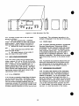
DC Power Supply
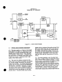
HP Model 6296A
Operating and Service Manual
•
tlf~ .~\ 0
.....--- ----F/ /#1 HEWLETT _ _ _ __
~~PACKARD
OPERATING AND
SERVICE MANUAL
DC POWER SUPPLY
HP MODEL 6296A
HP Part No. 06296-90001
SERIAL NUMBER PREFIX 60
I
QTS U BR /\ fW
I
ONE YEAR WARRANTY
This HP product has a one year warranty. P!eue rept.:e the
first paragraph of the warranty et.atement on the inside front
COYer
with. the following:
Thia Hewlett·Pacbrd hardware product is warranted
against deftds in mataial GUI worlananship for a
period of one year from date of delivl'ry. HP software
ud firmware products, which are designated by HP
for me with a hudware product and when property
installed on that hardware product. are Waftaftted not
to fail to execute their programming instruc:tiDN due
to defects in a\aterial and worknwWtip for a period
of 90 days from date of delivery. If HP receives notice
of such defects during the wmanty period, HP shall
ftPair or repi.:e software meda and firmware which
do not execvte their progrmnming iN1nlCtioM due to
such defeds. HP does not warrant that the operation
for the software, finnw.mre or hardware lhall be
uninterrupted or mor free.
CALL CENTER LIBRARY
11110 llH
/U 11111 ml 111111~
~~11111111111111111111111
2400013351
Printed: December, 1961
CERTIFICATION
Hewlett-Packard Company certifies that this product met its published specffications at time of shipment from the factory.
Hewlett-Packard further certifies that its calibration measurements are traceable to the United States National Bureau 1af
Standards, to the extent allowed by the Bureau's calibration facility, and to the calibration facilities of other International
Standards Organization members.
•
WARRANTY
This Hewlett-Packard hardware product is warranted against defects in material and workmanship for a period of one ve•ar
from date of delivery. HP software and firmware products, which are designated by HP for use with a hardware produ'ct
and when properly installed on that hardware product, are warranted not to fail to execute their programming instructions
due to defects in material and workmanship for a period of 90 days from date of delivery. During the warranty period, HP
Company will, at its option, either repair or replace products which prove to be defective. HP does not warrant that the
operation of the software, firmware, or hardware shall be uninterrupted or error free.
For warranty service, with the exception of warranty options, this product must be returned to a service facility designated
by HP. Customer shall prepay shipping charges by (and shall pay all duty and taxes) for products returned to HP for warran1ty
service. Except for products returned to Customer from another country, HP shall pay for return of products to Customer.
Warranty services outside the country of initial purchase are included in HP's product price only if Customer pays HP international prices (defined as destination local currency price, or U.S. or Geneva Expon price>.
If HP is unable, within a reasonable time, to repair or replace any product to a condition as warranted, the Customer shall
be entitled to a refund of the purchase price upon return of the product to HP.
LIMITATION OF WARRANTY
The foregoing warranty shall not apply to defects resulting from improper or inadequate maintenance by the Customer,
Customer-supplied software or interfacing, unauthorized modification or misuse, operation outside of the environmental
specifications for the product, or improper site preparation and maintenance. NO OTHER WARRANTY IS EXPRESSED OR
IMPLIED. HP SPECIFCALLY DISCLAIMS THE IMPLIED WARRANTIES OF MERCHANTABILITY AND FITNESS FOR .A
PARTICULAR PURPOSE.
•
EXCLUSIVE REMEDIES
THE REMEDIES PROVIDED HEREIN ARE THE CUSTOMER'S SOLE AND EXLCUSIVE REMEDIES. HP SHALL NOT BE
LIABLE FOR ANY DIRECT, INDIRECT, SPECIAL, INCIDENTAL, OR CONSEQUENTIAL DAMAGES, WHETHER BASED
ON CONTRACT, TORT, OR ANY OTHER LEGAL THEORY.
ASSISTANCE
The above statements apply only to the standard product warranty. Warranty options, extended support contracts, produ1:t
maintenance agreement$ and customer a$$i$tance 11g1eement$ are also Bvai/able. Contact your nearest Hewlett-Packard Sales
and Service office for further information on HP's fuU line of Support Programs.
·
·
•
MANUAL CHANGES
Model 6296A DC Power Supply ·
· Manual HP Part No. 06296-90001
•
Change Date 10/03/90
Make all corrections in the manual according to errata below, then check the following
table for your power supply serial number and enter any listed change(s) in the manual.
MAKE
SERIAL
ERRATA
:----------•-------------:I CHANGES
Number
: Prefix
In Table 1-1 (and paragraph 5-20), change
the INTERNAL IMPEDANCE AS A CONSTANT VOLTAGE
SOURCE (Output Impedance) specification to
read:
"OUTPl1l'
IMPEDANCE
{TYPICAL):
Approximated by a 5 milliohm resistance in
series with a 1 microhenry inductance.
I
·----------------------·--------ALL
------- ERRATA
60
00231-00260
1
60
70
70
7M
7M
7H
7M
7M
7H
•
•
1140A
1140A
1140A
1551A
1552A
1730A
1807A
1816A
1834A
1918A
1929A
2114A
2133A
2234A
2410A
2631A
2841A
2933A
3003A
3024A
I
00261-00290
1,2
00291-00320
1,2,3
1-4
00321-00350
00351-00380
1-5
00381-00410
1-6
00411-00522
1-7
00523-00612
1-8
00613-00712
1-9
1-10
00713-01776
01777-01796
1-11
01797-01816
1-12
01817-02411
1-13
02412-02419
1-14
02420-02776
1-15
02777-02956
1-16
02957-02986
1-17
02987-03146
1-18
03147-03386 I 1-19
1-20
03387-03545
1-21
03547-04086
04087-04246 1-22,•23
04247-04486
1-23
04487-04926
1-24
04927-05566
1-25
05567-05916
1-26
05917-06036
1-27
06037-06146
1-28
06147-06206
1-29
06207-up
1-27,29,
30
On page 3-2, Figure 3-4, disconnect strap
between terminals A4 and A5. and connect A5
to +S. On page 3-3, Figure 3-6, disconnect
strap between terminals A7 and AS and connect A8 +S.
Add the following note to paragraph 3-18 on
page 3-2 and to paragraph 4-41 on page 4-7:
"A protection circuit which protects the
series regulator from overload damage is activated whenever: (1) a. short is placed
across the supply, or (2) the output is
rapidly down progranmed by an increment of
more than 4 to 10 volts. When activated,
the protection circuit limits the supply's
output current to about 101 of rating for a
period of from 0.5 to 10 seconds depending
on the model and the load conditions."
page 5-6, paragraph 5-22, change steps a
and f as follows:
a. Connect test setup shown in Figure 5-4
with switch 51 closed.
f. Insert load resistor (Ry) by opening
switch S1. Also, add the following note:
"The short circuit protection circuit in
this supply will be activated if switch
: S1 is closed instead of opened during
· this test."
On
I
I
I
I
I
I
I
page 5-8, in Step 3 of Table 5-4, change
the text to read : "If it 1s not, proceed to
Step 4."
On
----------------------------------
1
Page 2 - HP P/N 06296-90001 changes - continue d
ERRATA
ERRATA
In the parts list on page 6-5:
Change C501 to HP P/N 0160-07 10.
Change C200 to fxd film .01 uF, 200 V,
HP P/N 0160-0161.
Change the listing for Q702, 800, 850, 852,
853 to 2N2907A, Sprague 56289, HP P/I 1853
-0099.·
.change the part number for C803 to 0180-1986
and its voltage rating to 85 V•
. Add pilot light DSl HP P/N 1450-05 66.
Change SCR CR502 and CR504 from HP P/N 18840019 to P/N 1884-03 47.
On the schemat ic diagram , indicate tbat t .
nominal value for R313 is 1 k. ThE! exa
·value for R313 is factory selected to optimize the range of transien t adj\l.st pot
R307.
In Appendix A, change Figure A-1 Overvol tage
Protecti on Crowbar to appear as shown below:
DC POWEii Sll'Pl.Y 62-...
en ,Page 6-T:
Add R865, var ww 250 ohm, HP P/N 2100-0439.
Also add Spacer-r ound, HP P/N 0380-1551
and Internal -externa l lockwas her, BP P/H
2190-057 6.
Delete the two types of binding posts list
and add the followin g:
black binding post, HP P/N 1510-01 14,
qty. 2
red binding post, HP P/N 1510-01 15.
Add: Insulato r (CR502, 504), .HP P/H 5020
-5595.
For all instrume nts delivere d on or after
July 1, 1978, change the HP P/N for
fusehold er from 1400-008 4 to fusehold er body
2110-056 4 and fuseh.o1 der carrier 2110-0565.
•
On page 6-7:
Change the HP P/N for fusehol der nut from
2950-0038 to 2110-056 9. If' old fusehold er
must be replaced for any reason, replace
complet e · fusehold er and nut with new
fusebold er parts. Do not replace new parts
with old parts.
On page 6-8, note that effectiv e January 1.
1971, Options 007 (10-turn voltage control)
and 008 (10-turn current control ) are . no
longer availabl e individ ually, but are still
availab le combined as Option 009. Likewise
Options 013 (10-turn voltage control with
decadia l) are · no longer availab le individua lly, but are availab le combined into
a single new option designa ted Option 015.
Make these changes whereve r Option 007 •. 008,
013, or 014 is mentione d in the manual.
•
2
' Page 3 ·-HP P/N.06296-90001 changes - continued
CHANGE ·1
CHANGE 4
Jaif:..
page 6-5, change C500 from 10,000 uF to
~,000 uF, HP P/N 0180-1929.
·
Make the following changes in the parts
list:
Add new diode CR603, 1N485B, HP P/N 19010033.
Change R313 to 1 k, 5% (selected) 1/2 W, HP
P/N 0686-1025.
Change R707 to 2 W, I.R.C. Type·BWH, HP P/N
0811-1674.
Change R601 to 422 ohm, 1/4 W, HP P/N 069811590.
CHANGE 2
On the component location drawing (schematic
apron) make the following changes:
a. Interchange collector (C) and emitter
(E) designations for transistor Q853 on
the lower right hand side of drawing.
b. Remove TP21 designation from R205 on
center left hand side of drawing. The
TP21 designation at the bottom of R310
is unchanged.
c. TP19 (bottom center) should point to
bottom of R300.
d •. Interchange locations of Q401 and CR809
at bottom left of drawing. Electrical
connections remain the same.
Change R870 to 5 k pot, HP P/N 2100-1824.
Change R871 to 750 ohm, 11, HP P/N 07570420.
Delete R872.
Add new Zener diode VR800, 4.22 V, HP PIN
1902-3070.
Q-1 the schematic, delete ·R872 in the meter
circuit and connect VR800 in its place. The
anode of VRSOO goes to base of Q850 and
cathode goes to +15.4 V reference. Also,
connect CR603 across VR600 in the reference
circuit. The anode of CR603 goes to +S and
the cathode goes to +9.4 volts.
CHANGE 3 .-
The serial number prefix of the instrument
has been changed from 6D to 70.
the parts list and on the schematic, make
e following changes: Add new resistor
402, 600 ohm, 5 W, HP P/N 0811-1860 across
R309 ( 150 ohm) • Change TSO 1 to HP P/N
9100-2184.
CHANGE 5
1lle serial number prefix of the instrument
has been changed from 7D to 7M. In the
parts list, delete S1 (switch/indicator,
ON/OFF) and replace with a separate toggle
switch and pilot light as follows:
51, toggle switch, Carling, 2FA53-73-SKI,
HP P/N 3101-0984.
DS1, pilot light, Neon, Sloan, HP P/N
1450-0048.
.
Schematic connections to the new switch and
pilot light remain the same except that the
two are physcially separate.
On the schematic, the primary of bias transformer T801 should be connected as shown in
the following sketch for 115 Vac operation.
For 230 Vac operation, the jumpers between
lugs 1 and 3, and 2 and 4 must be removed,
and lugs 2 and 3 connected together. In addition, a new power transformer, TSOO, must
be installed in accordance with Option 18.
TIOI
•
3
Page 4 - HP P/N 06296-90001 changes - continued
;
--------------------------------------------------------------------HP PART NO.
DESCRIPTION
:-------------------------------OPTION
------------·
: STANDARD
l OPTION A85
X95
----------- Lettered :------------:--------------:-Front Panel,----------: 06296-60004
06296-60001
: ----------<------------
Heat Sink Assembly
,Rear Chassis
:eover, Top
:chassis, Right Side
:chassis, Left Side
5060-7968
5000-9485
5000-9431
5000-9406
5000-9407
<-----~--<---~----<-----~-~
:
::
<-----~---
;
<----------
:
•
5060-6131
5000-6103
5000-6104.
5000-6098
5000-6099
------------------------------------------------------------CHANGE
---------13 (Cont)
CHANGE 6
Option X95 designates use of the former
color scheme of light gray and blue gray.
Option A85 designates use of a light gray
front panel with olive gray used for all
other external surfaces. New part numbers
are shown above.
·
the parts list, change R309 to 125 ohm,
40 W, HP P/N 0811-2621.
In
CHANGE 7
In the parts list, change R826 to 3.9 k, 5S,
1/2 W, HP P/N 0686-3925.
CHANGE 14
CHANGE 8
All primary ac connections have been removed
from the circuit board and are now made
directly to the transformer primaries. R903
has been removed from the PC board and is
now on a new terminal strip (0360-1696) •
mounted on the SCR heatsink assembly. Th1ese
chan~es do not affect the circuit schematic.
the parts list, change R816 to 56 k, 5S,
1/2 W, AB, HP P/N 0686-5635.
In
CHANGE 9
In the parts list and on the schematic,
change R501 and R502 to 22 ohm, 51, 1/2 W,
HP P/N 0686-2205.
CHANGE 15
TSOO has been replaced by a new transforiner
with a dual-winding primary for 115/ 230 Vac
operation. The new transformer CHP l?/N
06296-80091) replaces both TSOO transfonn1!rs
previously used in this model for 115 V or
230 V operation.
CHANGE 10
In the parts list, delete Cable Clamp, HP
PIN 1400-0332, qty. 2, and add Terminal
Strip, HP P/N 0360-0417.
CHANGE 11
Since it is no longer necessary to replace
TSOO to convert the supply from 115 to 230 V
operation or vice-versa, Option 018 (whJLch
equipped the supply for 230 V operation cmly) has been replaced by a new optie>n,
Option 028. In the replaceable parts li~>t,
remove R903 CHP P/N 0686-1245) (qty 1).
The serial prefix of the supply has been
changed to 1140A. 1his is the only change.
CHANGE 12
In the replaceable parts list and on the
schematic, change R702 to 1.5 k, ww, 3 W, HP
P/N 0811-1805, and change R709 to 1.6 k, 5S,
1/2 WHP P/N 0686-1625.
Option -028 modifies the standard 115 V unit
to a 230 V unit as described below. To ccmvert the supply for 230 V operation:
a. Remove the jumpers from between
terminals terminals 1 and 3, and 2 arid . •
4 of T800.
b. Install a jumper between terminals 2
and 3 of T800.
·
c. Replace F1 with a 3A 250 V fuse
(2100-0003).
CHANGE 13
The standard colors for this instrument are
now mint gray (for front panels and rear
panels) and olive gray (for all top, bottom,
side, and other external surfaces).
4
~age 5 - HP P/N 06296-9000·i changes - continued
~
Note: Due to the circuit changes shown.on
the next figure, it is no longer necessary
change any jumper connections at T801.
~
dual primary windings of T801 are perently wired in parallel across winding
3-4 of T800. The pilot light, in series with
R903, is also connected across th1 s winding.
I
·~{
AS-
AC
~·
..--;_ _ _ _ N
·CHANGE 19 (Cont)
lhe procedure for selecting R712 is identical to the one given for 50 Hz operation in
paragraph 5-55, steps g through j, except
that the resistance value should be selected
to ·provide a 3 V +/-.2 V drop across the
·series regulator. (For 50 Hz operation, the
voltage drop across the series regulator
remains 3.5 V) Center R711 before using the
resistance box to determine the value for
R712 •.
Also change VR600 to 9 V, HP P/N 1902-0785,
change R606 to 9 k, HP P/N 698-5454, and
change R611 to 490 ohm, 3 W, HP P/N
0811-1801.
CIRCUIT PATENTS APPLIED
FOR LICENSE TO USE MUST
BE OBTAINED IN WRITING FROM
HEWLETT-PACKARD CO.
HARRISON DIVISION.
CHANGE 16
the parts list and on ~he schematic,
change R307 to 10 k, 10S, HP P/N 2100-3210.
In
NOTES:
CHANGE 17
1. All resistors are in ohms, 1/2W, +5$
~the
uness otherwise noted.
2. All capacitors are in microfarads
unless otherwise noted.
parts list and on the schematic, add
capacitor C901, 0.1 uF, 250 V. HP P/N
016Q-~0.65 as shown below:
N:.c----------
CHANGE 20
In the parts. list and on the schematic for
the overvoltage protection crowbar, delete
R1 and VR1; add U1 voltage regulator, HP P/N
1826-0276 and C2, fxd elect, 1 uF, 50 V, HP
PlN 0180-0230; and change R9 to 1.5 k, HP
P/N 0757-0427 and R10 to 1.5 k, 5$, HP P/N
0811-1805 as shown in the schematic.below:
C901
F1
·~~~-----------
""'"'
CHANGE 18
s
+l~.411
In the parts list and on the schematic, add
resistor· R904, 10 ohm, 5S, 1/2 W, HP P/N
0686-1005 in series with the negative lead
of capacitor C801.
CZ
CHANGE 19
~
the replaceable parts list and on the
indicate that 12 k is the nominal
value for R712. 1be value for R712 is factory s.elected to optimize the range of ramp
adjust pot R711.
~atic,
5
~
•
•
Page 6 - HP PIN 06296-90001 changes - continued
CHANGE 21
CHANGE 27
In the replace able parts list, change the HP
PIN's for the binding posts and associa~ed
hardware to the follow ing: Red binding post,
qty. 2, 1510-0091; Terminal lug, qty. 2,
0360-0042; Lockwasher, qty. 2, 2190-0079;
Nut, qty 2, 2500-0001; .Black binding post,
qty 1, 1510-0107;·'· Terminal lug, qty. 1,
0360-1190; Nut, qty. 3, 2950-0144.
In the replace able parts list, change t h .
part number for the bias transformer from H
P/N 9100-2184 to HP P/N 9100-4751. Note
that the primary wiring colors have changed,
the white/grey is now black/yellow a1:ld the
grey is now black. See the figure below.
Figure 28a • Transformer Q:innec:tions
For 115 v.c 0Pltl11on
.CHANGE 22
In the replace able parts list on page 6-7,
change S1 (previo usly changed in Change 5)
to HP PIN 3101-2456. On page 6-5, change Q40
to HP PIN 1854-0458.
··-..
-
~
~:y~-~
CHANGE 23
• 'fllis change also applie s to units with
serial numbers 2114A-4177; 4190, and 4240.
-
-
=---
...··-·
,........ ~
'-
In the replac eable parts list and on the
schematic for the overvo ltage protec tion
crowbar, make the follow ing changes: Change
C2 (added in Change 20) to 2.2 uF, 20 V, HP
PIN 0180-0155.
CHANGE 28
In the replace able parts list, change~ Q40 .
from HP P/N 1854-1124 to HP PIN 1854-0!158.
Add C3, fxd cer, 0.01 uF, 10S, 100 V, HP PIN
0160-4832. . It is to be mounted between the
cathode or CR1 and the anode of CR2.
CHANGE 29
In the replace able parts list, change the
part number for Q851 from HP PIN 185!~-0221
to HP PIN 1854-0229.
Change CR4 to a two junctio n stabis tor, HP
PIN 1901-0701.
CHANGE 24
CHANGE 30
In the replace able parts list on page 64),
change R605 to 6.8 k, HP PIN 0757-0750.
In the replace able parts list, change! Q400
to HP PIN 06296-80004. Use this part r.tumber
for replacement on all units.
CHANGE 25
In the replace able parts list, page 6-7 add
the follow ing mechanical assembly; Barrie r
Strip Guard Assembly HP .PIN 5060-2862, qty
1.
CHANGE 26
In the replac eable parts list, page 6-5,
change Q400 to HP P/N 1854-1124 QTY 1, and
Q303 to HP P/N 1854-1017.
•
6
•
SAFETY SUMMARY
The following general safety precautions must be observed during all phases of operation, service, and repair of this instrument.
Failure to comply with these precautions or with specific warnings elsewhere in this manual violates safety standards of dnign,
manufacture, and intended use of the instrument. Hewlett-Packllrd Company assumes no liability for the customer's failure to
comply with these requirements.
BEFORE APPLYING POWER
SAFETY SYMBOLS
Verify that the product is set to match the available line voltage.
Instruction manual symbol: the product will
be marked with this symbol when it is
necessary for the user to refer to the
instruction manual (refer to Table of
Contents).
GROUND THE INSTRUMENT
This product is a Safety Class 1 instrument (provided with a
protective earth terminal). To minimize shock hazard, the
instrument chassis and cabinet must be connected to an
electrical ground. The instrument must be connected to the ac
power supply mains through a three-conductor power cable,
with the third wire firmly connected to an electrical ground
(safety ground) at the power outlet. Any interruption of the
protective (grounding! conductor or disconnection of the
protective earth terminal will cause a potential shock hazard
that could result in personal injury. If the instrument is to be
energized .via an external autotransformer for voltage reduction,
be certain that the autotransformer common terminal is
connected to the neutral !earthed pole) of the ac power lines
(supply mains!. This instrument is equipped with a line filter
·to reduce electromagnetic interference (EMii, and must be
connected to a property grounded receptacle to minimize EMI.
•
FUSES ·
Fuses are contained inside the unit, and are not userreplaceable. Only trained service personnel should replace blown
fuses, and only after identifying and correcting the problem
which caused the fuse(s) to blow.
DO NOT OPERATE IN AN EXPLOSIVE
ATMOSPHERE
Do not operate the instrument in the presence of flammable
gases or fumes.
KEEP AWAY FROM LIVE CIRCUITS
Operating personnel must not remove instrument covers.
Component replacement and internal adjClstments must be
made by qualified service pei-sonnel. Do not replace components
with the power cable connected. Under certain conditions,
dangerous voltages may exist even with the power cable
removed. To avoid injuries, always disconnect power, discharge
circuits and remove external voltage sources before touching
components.
Indicates hazardous voltages.
@
or
.I.
or
Warning
0
(CAUTION!
or
Caution
I
Indicate earth (ground) terminal.
The WARNING sign denotes a hazard. It
calls attention to a procedure, practice, or
the like, which, if not correctly performed
or adhered to, could result in personal
injury. Do not proceed beyond a
WARNING sign until the indicated
conditions are fully understood and met.
The CAUTION sign denotes a hazard. It
calls attention to an operating procedure,
or the like, which, if not correctly
performed or adhered to, could result in
damage to or destruction of part or all of
the product. Do not proceed beyond a
CAUTION sign until the indicated
conditions are fully understood and met.
DO NOT CIRCUMVENT SAFETY DEVICES
AC mains power exists on exposed terminals in various locations
in the mainframe and on the load modules. To protect the user
against the danger of electric shock, the unit is equipped with
a safety interlock that removes ac mains power when the top
cover is removed. Do not attempt to defeat the function of the
safety interlock.
DO NOT SERVICE OR ADJUST ALONE
Do not attempt internal service or adjustment unless another
person, capable of rendering first aid and resuscitation, is
present.
DO NOT EXCEED INPUT RATINGS
•
Operation at line voltages or frequencies in excess of those
stated on the data plate may cause leakage currents in excess of
3.5 mA peak .
DO NOT SUBSTITUTE PARTS OR MODIFY
INSTRUMENT
Because of the danger of introducing additional hazards, do not
install substitute parts or perform any unauthorized modification
to the instrument. Return the instrument to a Hewlett-Packard
Sales and Service Office for service and repair to ensure that
safety features are maintained.
Instruments which appear damaged or defective should be made inoperative and sscured against unintended operation unril they
can be repaired by qualified service personnel.
TABLE OF CONTENTS
Section
Pa~1e No.
IV PRINCIPLES OF OPERATION
4-8 Simplified Schematic
'l-3
4-3
4-10 Detailed Circuit Analysis
4-11 Preregulator and Control Circuit•l-3
•l-5
4-19 Series Regula tor
4-21 Constant Voltage Input Circuit 41-5
4-26 ConstantCurrent Input Circuit •l-6
<l-7
4-31 Gating Circuit
4-7
4-34 Error Amplifiers
4-7
4-37 Fault Input Circuit
·~-8
4-42 Reference Circuit
4-46 Meter Circuit
·1-8
Page No.
Section
1-1
I GENERAL INFORMATION
1-1
1-l DescriptiOn
1-6 Specifications
1-1
1-1
1-8 Options
1-2
1-10 Accessories
1-2
1-12 Instrument Identification
1-2
1-15 Ordering Additional Manuals
II
III
IV
INSTALIATION
2-1 Initial Inspection
2-3 Mechanical Check
2-5 Electrical Check
2-7 Installation Data
2-9 Location
2-11 Rack Mounting
2-15 Input Power Requirements
2-17 SOHz Operation
2-19 Power Cable
2-22 Repackaging for Shipment
2-1
2-1
2-1
2-1
2-1
2-1
2-1
2-2
2-2
2-2
2-2
v
3-1
OPERATING INSTRUCTIONS
3-1 Operating Controls and
3-1
Indicators
3-1
3-3 Operating Modes
3-1
3-S Normal Operating Mode
3-1
3-7 Constant Voltage.
3-1
3-9 Constant Current
3-2
3-11 Connecting Load
3-14 Operation of Supply Beyond
3-2
Rated Output
3-2
3-16 Optional Operating Modes
3-17 Remote Programming. Constant
3-2
Voltage
3-24 Remote Programming. Constant
3-3
Current
3-3
3-30 Remote S.ensing
3-4
3-35 Series Operation
3-5
3-39 Parallel Operation
3-5
3-42 Auto-Tracking Operation
3-45 Special Operating Cons1derat10ns3-6
3-6
3-46 Pulse Loadin;
3-6
3-48 Output Capacitance
3-6
3-51 Reverse Voltage Loading
3-6
3-53 Reverse Current Loading
PRINCIPLES OF OPERATION
Overall Block Diagram
Discussion
MAINTENANCE
5-1 Introduction
S-3 General Measurement
Techniques
5-:.8 Test Equipment Required
s-10 Performance Test
5-12 Constant Voltage Tests
S-21 Constant Current Tests
S-25 Troubleshooting
5-27 Trouble Analysis
S-34 Repair and Replacement
S-36 Adjustment and Calibration
S-38 Meter Zero
S-40 Voltmeter Tracking
S-42 Ammeter Tracking
S-44 Constant Voltage Programming
Current
S-46 Constant Current Programming
Current
S-48 Overvoltage Trip
S-50 Transient Recovery Time
S-52 Preregulator Tracking (60 Hz
Operation)
S-54 Preregulator Tracking (SO Hz
Operation)
VI REPIACEABLE PARTS
6-1 Introduction
6-4
6-8
4-1
4-1
Ordering Information
Reference Designators
Abbreviations
Manufacturers
Code List of Manufacturers
Parts List Table
•
s-1
S-1
!S-1
:S-1
:S-3
S-4
S-6
S-6
S-7
S-7
S-13
S-13
S-13
S-13
•
S-14
S-14
S-14
S-14
5-14
5-14
6-1
6-1
6-1
6-2
4-1
11
•
•
SECTION I
GENERAL INFORMATION
1-1
•
c. Series and Auto-Series Operation
DESCRIPTION
1-2 This power supply is completely transistorized and suitable for either bench or
relay rack operation. It is a compact, well-regulated. Constant Voltage/ Constant Current supply
that will furnish full rated output voltage at the
maximum rated output current or can be conUnuous1y adjusted throughout the output range. The front
panel CURRENT controls can be used to establish
the output current limit (overload or shon circuit)
when the supply is used as a constant voltage
source and the VOLTAGE control can be uaed to
establish the voltage limit (ce1Ung) when the supply is used as a constant current source. The
supply will automatically crossover from constant
voltage to constant current operation and Vice
versa if the output CUITant or voltage exceeds these
preset limits.
Power supplies may be used in series
when a higher output voltage is required in the
voltage mode of operation or when greater voltage
compliance is required in the constant current
mode of operation. Auto-Series operation permits
one knob control of the total output voltage from a
"master" supply.
1-3 The power supply has both front and rear
terminals. Either the positive or negative output
terminal may be qrounded or the power supply can
be operated floating at up to a maximum of 300
volts off ground.
The power supply may be used as a
"master" supply. havin9 control over one (or
more) "slave" supplies that furnish various
voltages for a system.
e. Auto-Track1n9
SPECifJCATIONS·
1-7 Detailed specifications for the power supply
are given in Table 1-1.
i-s omoNS
1-S Barrier strip terminals located at the rear of
the unit allow ease in adapting to the many operational capabiUU~s of the power supply. A brief
description of these capabilities is given below:
1-9 Options are factory modifications of a
standard instrument that are requested by the
customer. The follOWirlCJ options are available
for the instrument covered by this manual.
Where necessary. detailed covera9e of the options
is included throughout the manual.
a. Remote Programming
The power supply may be programmed
from a remote location by means of an external
Option No.
voltage source or resistance.
•
Parallel and Auto-Parallel Qperation
The power supply may be operated in
parallel with a similar unit when greater output
current capability is required. Auto-Parallel operation permits one knob control of the total output current from a "master" supply.
1-6
1-4 A single meter is used to measure either output voltage or output current in one of two ranges.
The voltage or current ranges are selected by a
METER switch on the front panel.
b.
d.
OS
Remote Sensing
The degradation in regulation which
would occur at the load because of the voltage
drop in the load leads can be reduced by using the
power supply in the ·remote sensing mode of operation.
1-1
Description
SO Hz Regulator Realignment:
Standard instruments will operate
saUsfactorily at both 60 and 50 Hz
without adjustment. However Option 05 factory reall9nment results
in more efficient operation at 50 Hz,
and is recommended for all applications when continuous operation from
a SO Hz ae input is intended .
Description
Option No.
07
08
09
c:lres ses).
i
Voltage 10-Tum Control: A single
control that replaces both coarse and
fine voltage controls and improves
output settability.
Current l '7'-Turn Control: A single
control that replaces both coarse and
fine current controls and improves
output settablllty.
Voltage and Current 10-Tum Controls: Options 07 and 08 on same
instrument.
11
Intema 1 Overvoltage Protection
"Crowbar". Operating and Service
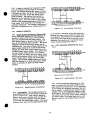
information is included 1n Appendix A
at the rear of the manua 1.
13
Three Digit Graduated Decadial
Voltage Control: Control that replaces 10-tum voltage control permitting accurate resettability.
14
Three Digit Graduated Decadial
•
Description
14SlSA
Rack Kit for mounting one Si"
high supply. (Refer to Section II
for details. )
1452SA
Rack Kit for mounting two Si"
high supplies. (Refer to Section II
for details. )
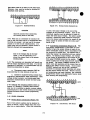
1-12 INSTRUMENT IDENTIFICATION
1-13 Hewlett-Packard power supplies are identified by a three-part serial number tag. The first
part is the power supply model number. The i;econd part is the serial number prefix, which co•nsists of a number-letter combination that denc>tes
the date of a significant design change. The number designates the year, and th,e letter A through M
designates the month, January.through December
respectively. The third part is the power supply
serial number.
1-14 If the serial number prefix on your power
supply does not agree with the prefix on the title
page of this manual, change sheets are included
to update the manual. Where applicable, bac:kdating information is given in an appendix at the
rear of the manual.
Current Control: Control that replaces coarse and fine current controls permitting accurate resettability.
18
Part No.
230V AC, Single Phase, Input:• Supply is shipped for llSV ac operation.
Option 18 consists of modifying the
supply for 230Vac operation.
1-lS ORDERING ADDITIONAL
MANU~
•
1-16 One manual is shipped with each power
supply. Additional manuals may be purchased
from your local Hewlett-Packard field office (see
list at rear of this manual for addresses). Specify
the model number, serial number prefix, and G~
stock number provided on the Utle page.
1-10 ACCESSORIES
1-11 The accessories listed in the following
chart may be ordered with the power supply or
separately from your local Hewlett-Packard field
sales office (refer to list at rear of manual for ad-
•
1-2
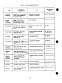
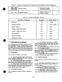
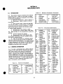
Table 1-1. Specifications
•
including a direct short placed across the terminals in constant voltage operation, The constant
voltage circuit limits the output voltage in the
constant current mode of operation.
INPUT:
105-125 VAC. single phase, 50-60Hz,
4. SA, 250W•
OUTPUT:
0-60 volts@ 0-3 amps.
METER:
The front panel meter can be used as either
a 0-70 or 0-7 volt voltmeter or as a 0-4 or 0-0. 4
amp ammeter.
LOAD REGULATION:
Constant Voltage -- Less than 0. 01% plus
l mV for a full load to no load change in output
current.
Constant Current -- Less than 0. 05% plus
lmA for a zero to maximum change in output
voltage.
LINE REGUIATION:
Constant Voltage -- Less than 0. 01%
lmV for any line voltage change within the
rating.
Constant Current -- Less than O. 05%
lmA for any line voltage change within the
rating,
OUTPUT CONTROLS:
Coarse and fine voltage controls and coarse
and fine current controls provide continuous adjustment over the entire output span.
OUTPUT TE™INALS:
Three "five-way" output posts are provided
on the front panel and an output terminal strip is
located on the rear of the chassis. .All power
supply output terminals are isolated from the
chassis and either the positive or negative terminal may be connected to the chassis through a
separate ground terminal. If the front panel terminals are used. the load regulation will be O.SmV
per ampere greater. due to the front terminal resistance.
plus
input
plus
input
RIPPLE AND NOISE:
Constant Voltage -- Less than 500t£V rms.
Constant Current -- Less than 3mA nns.
•
OPERATING TEMPERATURE RANGES:
Operating: o to sooc. Storage: -20 to +ssoc.
TEMPERATURE COEFFICIENT:
Constant Voltage -- Less than O. 02% plus
S0011V ?er degree Centigrade.
Constant Current -- Less than O. 02% plus
l. 5mA per degree Centigrade.
STABILI'IY:
Constant Voltage -- Less than 0.10% plus
2. 5mV total drift for 8 hours after an initial warmup time of 30 minutes at constant ambient. constant line voltage. and constant load.
Constant Current -- Less than O. 10% plus
7. SmA total drift for 8 hours after an initial warmup time of 30 minutes at constant ambient, constant line voltage, and constant load.
INTERNAL IMPEDANCE AS A CONSTANT VOLTAGE
SOURCE:
Less than O. 001 ohm from DC to lOOHz.
Less than O. 01 ohm from lOOHz to lkHz.
Less than 0. 2 ohm from lkHz to lOOkHz.
Less than 2. 0 ohms f~m l 00 kHz to 1 MHz.
•
ERROR SENSING:
Error sensing is normally accomplished at
the front terminals if the load is attached td the
front or at the rear terminals if the load is attached to the rear terminals. Also. provision is included on the rear tenainal strip for remote sensing.
REMOTE PROGRAMMING:
Remote programming of the supply output at
approximately 300 ohms per volt in constant voltage is made available at the rear terminals. In
constant current mode of operation. the current
can be remotely programmed at approximately
500 ohms per ampere.
COOLING:
Convection cooling is employed. The supply has no moving parts.
SIZE:
5}" H x 16" D x Si" W. Two of the units
can be mounted side by side in a standard 19"
relay rack.
TRANSIENT RECOVERY TIME:
Less than 50~sec for output recovery to within 15 mv following a current change in the output
equal to the current rating of the supply or 5
amperes, whichever is smaller •
WEIGHT:
OVERLOAD PROTECTION:
A continuously acting constant current circuit protects the power supply for all overloads
POWER CORD:
A three-wire, five-foot power cord is provided with each unit.
1-3
29 lbs. net. 38 lbs. shipping.
FINISH:
Light gray front panel with dark. gray case.
•
SECTION II
INSTALLATION
2-1
INITIAL INSPECTION
2-2 Before shipmen t, this instrum ent was inspect ed
and found to be free of mechan ical and electric al
defects . As soon as the instrum ent is unpacke d, inspect for any damage that may have occurre d in
transit. Save all. packing materia ls until the inspection is complet ed. If damage is found. proceed as
describ ed in the Claim for Damage in Shipme nt section of the warrant y page at the rear of this manual.
MECHANICAL CHECK
2-4 This check should confirm that there are no
broken knobs or connec tors, that the cabinet and
panel surface s are free of dents and scratch es, and
that the meter is not scratch ed or cracked .
2-3
2-5
ELECTRICAL CHECK
2-6 The instrum ent should be checked against its
electric al specific ations. Section V include san"incabinet " perform ance check to verify proper instrum ent
operatio n.
INSTALLATION DATA
2-8 The instrum ent is shipped ready for bench
operatio n. It is necessa ry only to connect the in2-7
•
strumen t to a source of power and it is ready for
operatio n.
2-9
LOCATION
2-10· This instrum ent is air cooled. Sufficie nt space
should be allotted so that a free flow of cooling air
can reacn the sides anci rear of the ins trumenc when
itis inopera tion. It should be used in an area where
the ambient tempera ture does not exceed sooc.
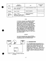
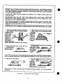
2-11 RACK MOUNTING
2-12 This instrum ent may be rack mounted in a
standar d 19 inch rack panel either alongsi de a similar unit or by itself. Figures 2-1 and 2-2 show how
both types of installa tions are accomp lished.
2-13 To mount two units side-by -side, proceed as
follows :
a. Remove the four screws from the front
panels of both units.
b. Slide rack mountin g ears between the
front panel and case of each unit.
c. Slide combini ng strip between the front
panels and cases of the two units.
d. After fastenin g rear portions of u_nits together using the bolt, nut, and spacer, replace panel- screws •
RAC!( EM
--
..
-·
6el
....
•
8
-0
-0
-· 0
COllllNlltG
STlllP
Figure 2-1. Rack Mounti ng, Two Units
2-1
-0
•
I
Q
....
ti
0
0
.1
cl
r-¥0L.TACE-,
C.OAAS( r1-.[
(j (j
0
10
•
c
I
Q
Figure 2-2. Rack Mounting, One Unit
be realigned. This realignment procedure is described in Paragraph 5-54 at the rear of the·manual.
2-14 To mount a single unit in the rack panel,
proceed as follows:
a. Bolt rack mounting ears. combining
straps, and angle brackets to each side of center
spacing panels. Angle brackets are placed behind combining straps as shown in Figure 2-2.
b. Remove four screws from front panel of
unit.
c. Slide combining strips between front
panel and case of unit.
d. Bolt angle brackets to front sides of
case and replace front panel screws.
2-19 POWER CABLE
2-20 To protect operating gersonnel, the National
Electrical Manufacturers' Association (NEMA)
recommends that the instrument panel and ca:binet
be grounded. This in&trument is equiPped with a
three conductor p01Ner cable. The third cond·uctor
•
is the ground conductor and when the cable is
plugged into an appropriate receptacle, the instrument is grounded. The offset pin on the power
cable three-prong connector is the ground connection.
2-15 INPUT POWER REQUIREMENTS
2-16 This power supply may be operated from
either a nominal 115 volt or 230 volt 50-60 cycle
power source. The unit, as shipped from the factory, is wired for 115 volt operation only. A
factory modification (Option 18) must be made to
permit operation from a 230 volt line. The input
power required when operated from a llS volt, 60
cycie power source at full load is given in the
s~ecification table in Section I.
2-21 To preserve the protection feature when operating the instrument from a two-contact outlet,
use a three-prong to two-prong adapter and c:onnect the green lead on the adapter to ground.
2-22 REPACKAGING FOR SHIPMENT
2-23 To insure safe shipment of the instrument,
it is recommended that the package designed for
the instrument be used. The original packaging
material is reusable, If it ls not available, contact your local Hewlett-Packard field office ~:o
obtain the materials. This office will also furnish
the address of the nearest service office to which
the iT\strument can be shipped. Be sure to attach
a tag to the instrument which specifies the o·wner, model number, full serial number, and SE~rvice
required, or a brief description of the troublE!.
2-17 SO Hz OPERATION
2-18 Theunit as normally shipped from the factory
can be operated from either a 50 or 60 Hz source.
However, with a 50 Hz input, the operation of the
unit may become somewhat deqraded when the
temperature exceeds 350 Centigrade (instead of the
normal soocentigrade capability with a 60 Hz input).
To permit optimum operation at 50 Hz, the unit must
2-2
•
•
SECTION III
OPERATING INSTRUCTIONS
OPERATING CONTROLS AND INDICATORS
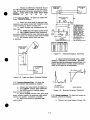
3-1
3-2 The front panel controls and indicators , together with the normal turn-on sequence, are
shCM'n in Figure 3-1.
0
ll(f(I
3-5
NORMAL OPERATING MODE
3-6 The power supply is normally shipped with
its rear terminal strapping connectio ns arranged
for Constant Voltage/C onstant Current, local
sensing, local programming, single unit mode of
operation . This strapping pattern is illustrated in
Figure 3-2. The operator selects either a constant
voltage or a constant current output using the front
panel controls Oocal programming, no strapping
changes are necessary }.
TURN-ON SEQUENCE
I.
2.
PUSH ON/OFF BUTTON ANO BUTTON SHOULO LIGHT.
SET METER SWITCH TO C&SIREO VOLTAGt llAN'GE.
Figure 3-2. Normal Strapping Pattern
ADJUST COARSE AND nNE VOLTAGE CONTROLS UNTIL lXSllED
OUTPUT VOLTAGE IS INOICATl:D ON METER•
~. SET METER SWITCH DESIRED CURRENT ltANGt AND SHORT CIR•
CUIT OUTPUT TERMINALS.
s. ADJUST CURRENT CONTROLS f'OR cc;nu;o OUTPUT ci.nuu:m.
~. R.CMOV!: SHORT AND CONNECT ~TO OUTPUT TERMINALS
ll'RONT OR REAR!.
3.
•
CONSTANT VOLTAGE
3-8 To select a ronstant voltage output, proceed
as follows:
Figure 3-1. Front Panel Controls and Indicators
3-3
•
3-7
a. Turn-on power supply and adjust
VOLTAGE controls for desired output voltage {output terminals open).
OPERAnNG MODES
b. Short output terminals and adjust CURRENT controls for maximum output current allowable (current limit), as determined by load conditions. If a load change causes the current limit to
be exceeded , the power supply will automatic ally
crossove r to constant current output at the preset
current limit and the output voltage will drop proportionate ly, In setting the current limit, allowance must be made for high peak current which can
cause unwanted cross-ove r. (Refer to Paragraph
3-46).
3-4 The power supply is desiqned so that its
mode of operation can be selected by making
strapping conne~tions between particular terminals
on the terminal strip at the rear of the power supply. The terminal designatio ns are stenciled in
white on the power supply above their respective
terminals . Although the strapping patterns Ulustrated in this section show the positive terminal
grounded, the operator can ground either terminal
or operate the power supply up to 300 vdc off
ground (floating). The following paragraph s describe the procedure s for utilizing the various
operation al capabiliti es of the power supply. A
more theoretica l descriptio n concerning the operational features of this supply is contained in a
power supply Applicatio n Manual and in various
Tech. Letters published by the Harrison Division.
Copies of these can be obtained from your local
Hewlett-P ackard field office.
3-9
CONSTANT CURRENT
3-10 To select a constant current output. pro·
ceed as follows:
a. Short output terminals and adjust CURRENT controls for desired output current.
3-1
b. Open output terminals and adjust
VOLTAGE controls for maximum output voltage allowable (voltage limit), as determined by load
conditions. If a load change causes the voltage
limit to be exceeded, the power supply will automatically crossover to constant voltage output at
the preset voltage limit and the output current will
drop proportionately . In setting the voltage limit,
allowance must be made for high peak voltages
which can cause unwanted crossover. (Refer to
Paragraph 3-46).
NOTE
When Model 6291A is operated continuously in the
crossover region. between Constant Voltage/Constant Current, the feedback loop may break into oscillation; particularly in the 0. SA to l. SA output
current range. Although the crossover region is not
usually an area of continuous operation, this problem can be eliminated, if necessary, by connecting
the emitter of Q300 to +S (instead of to the emitter
of Q301) and readjusting R307. Note that when this
is done, the transient recovery time of Model 6291A
must be derated to "SOµsec for recovery to within
25mV" (instead of lSmV).
3-11
CONNECTING LOAD
3-12 Each load should be connected to the power
supply output terminals using separate pairs of
connecting wires. This will minimize mutual coupling effects between loads and will retain full
advantage of the low output impedance of the
power supply. Each pair of connecting wires
should be as short as possible and twisted or
shielded to reduce noise pickup. (If shield is
used, connect one end to power supply ground
terminal and leave the other end unconnected. )
3-16
OPTIONAL OPERATING MODES
3-17 REMOTE PROGRAMMING, CONSTANT VOl~T
AGE
3-18 The constant voltage output of the power
supply can be programmed (controlled) from a
remote location if required. Either a resistance or
voltage source can be used for the programming
device. The wires connecting the programming
terminals of the supply to the remote programmir1g
device should be twisted or shielded to reduce
noise pick-up. The VOLTAGE controls on the
front panel are disabled according to the followi.ng
procedures.
~
~
~
+·
+
G -
-
~
~
M M M
~
M
1°1~1~1
PROGRAMMING
RESISTat
Figure 3-3. Remote Resistance Programming
(Constant Voltage)
3-19 Resistance Programming (Figure 3-3). In
this mode. the output voltage will vary at a rate
determined by the programming coefficient, 200
ohms per volt (300 ohms per volt for Model 6296A).
The output voltage will increase l volt for each
200 ohms (or 300 ohms) added in series with the
programming terminals. The programming coeffi-cient is determined by the pr09rammin9 current.
This current is factory adjusted to within 2% of
S ma (2% of 3. 3 ma for Model 6296A). If greater
programming accuracy is required, it may be
achieved by changing resistor R806.
3-13 If load consideration s require that the output power distribution terminals be remotely
located from the power supply, then the power
supply output terminals should be connected to
the remote distribution 'terminals via a pair of
twisted or shielded wlres and each load separately connected to the remote distribution terminals.
For this case. remote &ensing should be used
{Paragraph 3-30).
•
•
3-20 The output voltage of the power supply
should be zero volts z20 millivolts when zero
ohms is connected across the programming termi·nals.
3-21 To maintain the stability and temperature
coefficient of the power supply, use programmin~;
resistors that have stable, low noise, and low
temperature (less than 30 ppm per degree Centigrade) characteristic s. A switch can be used in
conjunction with various resistance values in order
to obtain discrete output voltages. The switch
should have make-before-b reak contacts to avoid
momentarily opening the programming terminals
during the switching interval.
3-14 OPERATION OF SUPPLY BEYOND RATED
OUTPUT
3-15 The shaded area on the front panel meter
face indicates the amount of output voltage or
current that is available in excess of the normal
output. Althouoh the supply can be operated in
this shaded region without being damaged, it cannot be guaranteed to meet all of its performance
specifications . Hawever, if the line voltage is
maintained above 115 Vac, the supply wil~proba
bly operate within its specifications .
3-22 Voltage Programming (Figure 3-4). Employ
the strapping pattern shown on Figure 3-4 for
voltage programming. In this mode, the output
voltage will vary in a 1 to 1 ratio with the pro-
3-2
. •
•
;ramming voltage (reference voltage) and the load
on the programming voltage source will not exceed
25 microamperes.
Al
46 A2
+
+
G
-
-
•S
AJ
A4 AS
A6
A7
Al
101~1r1m1
coefficient and stability specifications . A switch
may be used to set discrete values of output current. A make-before-b reak type of switch should
be used since the output current will exceed the
maximum rating of the power supply if the switch
contacts open during the switching interval.
CAUTION
If the programming terminals (Al and A7) should
VOLTAGE
open at any time durinq this mode, the output current will rise to a value that may damage the power
supply and/or the load. To avoid this possibility,
connect a lK resistor (1. SK for Models 6290A and
6296A) across the programming terminals. Like the
programming resistor, this resistor should be of the
low noise, low temperature coefficient type,
SOURCE
Figure 3-4. Remote Voltage Programminq
(Constant Voltage)
3-23 The impedance matching resistors (Rx) for
the programming voltage source should be approximately 1000 ohms to maintain the temperature and
stability specifications of the power supply.
3-28 Voltage Programming (Figure 3-6). In this
mode. the output current will vary linearly with
changes in the programming voltage. The programming voltage should not exceed 1. 5 volts.
Voltage in excess of 1. 5 volts will result in excessive power dissipation in the instrument and
possible damage,
3-24 REMOTE PROGRAMMING, CONSTANT CURRENT
3-25 Either a resistance or a voltage source can
be used to control the constant current output of
the supply. The CURRENT controls on the front
panel are disabled according to the following procedures •
•
VOLtACE
SOURCE
PROGRAMMING
lu:slStoR
Figure 3-6. Remote Voltage Programming
(Constant Current)
Fiqure 3-S. Remote Resistance Programming
(Constant .Current)
3-29 The output current will be the programming
voltage divided by the internal current sampling
resistance RSOO. The current required from the
voltage source will be less than 10 microamperes.
The impedance matching resistor (Rx) should be
approximately 1000 ohms if the temperature coefficient and stability specifications of the power
supply are to be maintained.
3-26 Resistance Pn?qrammins (Figure 3-5). In
this mode, the output current varies at a rate
determined by the programming coefficient -- 100
ohms per ampere for Models 6282A and 6286A, 200
ohms per ampere for Models 6285A and 6291A, and
500 ohms per ampere for Models 6290A and 6296A.
The programming coefficient ls determined by the
Constant Current programming current l mA for
Models ~282A, 6285A, 6286A, and 6291A or O. 66
mA for Models 6290A and 6296A. This current is
adjusted to within 10% at the factory. If qreater
programming accuracy is required, it may be
achieved by changing resistor R808 as outlined in
Section V.
•
3-30
REMOTE SENSING (See Figure 3-7)
3-31 Remote sensing is used to maintain good
regulation at the load and reduce the degradation
of regulation which would occur due to the voltage
drop in the leads between the power supply and
the load. Remote sensing is accomplished by
utilizing the strapping pattern shown in Figure
3-7. The power supply should be turned off before
changing strapping patterns. It is not required
3-27 Use stable, low noise, low temperature coefficient (less than 30 ppm/Oc) programming resistors to maintain the power supply temperature
3-3
r"Al"""'l"'--r~r--.,..-..,.;;;...----....-..--.....-..,.;.;;~A6.;;.,.;117
that these leads be as heavy as the load leads.
However, they must be twisted or shielded to
minimize noise pick-up.
U
~~~~c@
0
•
Fiqure 3-7. Remote Sensing
Figure 3-8. Normal Series Connectii:>ns
CAUTION
is used, the output voltage is the sum of the
voltaqes of the individual supplies. Each: of the
individual supplies must be adjusted in oz'der to
obtain the total output voltage. The powe·r supply
contains a protective diode connected int~!mally
across the output which protects the supply if one
power supply is turned off while its serie:; partner(s) is on.
Observe polarity when connecting
the sensing leads to the load.
3-32 Note that it is desirable to minimize the
drop in the load leads and it is recommended that
th~ drop not exceed 1 volt per lead if the power
supply is to meet its DC specifications. If a
larger drop must be tolerated, please consult a
Hewlett-Packard field representative.
3-37 Auto-Series Connections (Figure 3-~ll.. The
Auto-Series configuration is used when it is desirable to have the output wltage of each of the
series connected supplies vary in accordc1nce with
the setting of a control unit. The control unit is
called the master; the controlled units arE! called
slaves. At maximum output voltage, the voltage
of the slaves is determined by the setting of the
front panel VOLTAGE control on the mastei~.
master supply must be the most positive supply
the series. The output CURRENT controls of all
series units are operative and the current limit is
equal to the lowest control setting. U any output
CURRENT controls are set too low, automatic
crossover to constant current operation wl.11 occur
and the output voltage will drop, Remote sensing
and programming can used: however, the strapping
arrangements shown in the applicable fig1J.res show
local sensing and programming.
NOTE
Due to the voltage drop in the load
leads, it may be necessary to readjust the current limit in the remote
sensing mode.
Th.
3-33 The procedure Just described will result in a
low DC output impedance at the load. If a low AC
impedance is required, it is recommended that the
following precautions be taken:
a. Disconnect output capacitor C803 by
disconnecting the strap between A2 and +s.
b. Connect a capacitor having similar characteristics (approximately same capacitance, same
voltage rating or greater, and having good high
frequency characteristics) across the load·using
short leads,
Al
0
MASTER
0
St.\VE
3-34 Although the strapping patterns shown in
Figures 3-3 through 3-6 employ local sensing,
note that it is possible to operate a power supply
simultaneously in the remote sensing and Constant
Voltage/Constant Current remote proqramming
modes.
3-35 SERIES OPERATION
3-36 Normal Series Connections (Figure 3-8).
Al
Two or more power supplies can be operated in
series to obtain a higher voltage than that available from a single supply. When this connection
Figure 3-9. Auto-Series, Two Units
3-4
•
•
3-38 In order to maint ain the tempe rature coeffi cient and stabil ity specif icatio ns of the pc)wer
supply , the extern al resist or (Rx) shown in Figure
3-9 should be stable , low noise, low tempe rature
coeffi cient (less than 30 ppm per degree Centi grade) resisto rs. The value of this resist or is
depen dant on the maximum voltag e rating of the
"mast er" supply . The value of Rx is this voltag e
divide d by the voltag e programming curren t of the
slave supply (l/Kp where Kp is the voltag e programming coeffi cient) . The voltag e contri bution of
the slave is determ ined by its voltag e contro l setting.
3-39
•
Figure 3-11. Auto- Parall el. Two Units
PARALLEL OPERATION
3-40 Normal Parall el Conne ctions (Figure 3-10).
Two or more power suppli es can be conne cted in
parall el to obtain a total outpu t curren t greate r
than that availa ble from one power supply , The
total outpu t curren t is the sum of the outpu t currents of the indivi dual power suppl ies. The output
CURRENT contro ls of each power supply can be
separa tely set. The output voltag e contro ls of one
power supply should be set to the desire d outpu t
voltag e: the other power supply should be set for
a slight ly larger outpu t voltag e. The supply set to
the lower output voltag e will act as a consta nt
voltag e source : the supply set to the higher output
will act as a consta nt curren t source , droppi ng its
outpu t voltag e until it equals that of the other
supply . The consta nt voltag e source will delive r
only that fractio n of its total rated outpu t curren t
which is neces sary to fulfill the total curren t
deman d.
to the maste r's regard less of the load condit ions.
Becau se the outpu t curren t contro ls ot each slave
are opera tive, they should be set to maximum to
avoid having the slave revert to consta nt curren t
operat ion: this would occur if the maste r output
curren t settin g excee ded the slave 's.
3-42 AUTO-TRACKING OPERATION (See Figure
3-12)
St.Avt
•MASTER MUST Bl: MOST FOS111VE SUPPLY
Figure 3-12.
Figure 3-10.
•
Auto-Tracki~g,
Two Units
3-43 The Auto-T rackin g config uratio n is used
when it is neces sary that severa l differ ent voltages referr ed to a common bus, vary in propor tion
to the settin g of a partic ular instru ment (the control or maste r). A fractio n of the maste r's outpu t
voltag e is fed to the compa rison ampli fier of the .
slave supply , thus contro lling the slave' s output
The maste r must have the larges t output voltag e of
any power supply in the group (must be the most
positi ve supply in the·ex ample shown on Figure
3-12).
Normal Parall el Conne ctions
3-41 Auto- Parall el. The strapp ing patter ns for
Auto- parall el operat ion of two power suppli es are
shown in Figure 3-11. Auto- Parall el operat ion
permi ts equal curren t sharin g under all load condition s, and allows compl ete contro l of outpu t
curren t fron:i one maste r power supply . The output
curren t of each slave will be approx imatel y equal
3-S
3-44 The output voltage of the slave is a percentage of the master's output voltage, and is determined by the voltage divider consisting of Rx and
the voltage control of the slave supply, Rp. where:
Es= Rp/Rx + Rp. Tum-on and tum-off the power
supplies is controlled by the master. Remote
sensing and programming can be used; although the
strapping patterns for these modes show only local
sensing and programming. In order to maintain the
temperature coefficient and stability specifications
of the power supply, the external resistors should
be stable, low noise, low temperature (less than
30 ppm per 0 c) resistors.
current is large enough to cause the constant cur-rent circuit to operate.
3-50 The effects of the output capacitor during •
constant current operation are as follows:
a. The output impedance of the power supply
decreases with increasing frequency.
b. The recovery time of the output voltage is
longer for load resistance changes.
c. A large surge current causing a high power dissipation in the load occurs when the load resistance is reduced rapidly.
3-45 SPECIAL OPERATING CONSIDERATIONS
3-51 REVERSE VOLTAGE LOADING
3-46 PULSE LOADING
3-52 A diode is connected across the output terminals. Under normal operating conditions, the
diode is reverse 'biased (anode connected to negative terminal). If a reverse voltage is applied to
the output terminals (positive voltage applied to
negative terminal), the diode will conduct, shunting current across the output terminals an1d limiting the voltage to the forward voltage drop of the
diode. This diode protects the series transistors
and the output electrolytic capacitor.
3-47 The power supply will automatically cross
over from constant voltage to constant current operation, or the reverse, in response to an increase
(over the preset limit) in the output current or voltage, respectively. Although the preset limit may
be set higher than the average output current or
voltage. high peak currents or voltages (as occur
in pulse loading) may exceed the preset limit and
cause crossover to occur. If this crossover limiting is not desired, set the preset limit for the
peak requirement and not the average.
3-5 3
3-48 OUTPUT CAPACITANCE
3-49 An internal capacitor, connected across the
output terminals of the power supply, helps to supply high-current pulses of short duration during
constant voltage operation. Any capacitance added
externally will improve the pulse current capability,
but will decrease the safety provided by the constant current circuit. A high-current pulse may
damage load components before the· average output
REVERSE CURRENT LOADING
3-54 Active loads connected to the poweir supply
may actually deliver a reverse current to the P°"'tA
supply during a portion of its oper~ting C}'Cle.
external source cannot be allowed to pump current
into the supply without loss of regulation and possible damage to the output capacitor. To avoid
these effects, it is necessary to preload the supply with a dummy load resistor so that thei power
supply delivers current through the entire operating cycle of the load device.
A19
•
3-6
•
SECTION IV
PRINCIPLES OF OPERATION
H
R£1'£RENCE
CIRCUIT
T
AC
I
FOWD
TRANS TORM DI
-
BIAS
SUPPLY
r--- REFERtNCE
VOLTAGES
-
8JAS
-VOLTAG ES
RECTIFIER/
I.
CURRENT
SAMPlJNG
"
RESJS10R
ERROii
AMPL.
•
SCA
-
L<J
FAULT
INPUT
CJRCIJIT
•
~
FEECIACl PATH
GATING
CIRCUIT
...
VOL?AGE
.,_ CONStAHT
INPUT
-
DC
OUTPUT
ClllCUIT -
T
COtmlOL
CJllCUJT
-
DENOTES VOLTAGE
-±
...
REGULATOR
....
MOTE:
....
SERIES
PllEREGUIJIlOR,
nLTER
-
CONSTANT CURRENT
INPUT
CIRCUIT
....
'
~
MtTER
CIRCUIT
...
•
l
-
,..
-
- - - DENOTES CURRENT
FtEDIACl MTH
Figure 4-1. Overall Block Diagram
4-1
plishes this by issuing a firing pulse to one of the
SCR's once during each half cycle of the input ac.
The control circuit continuo usly samples the output voltage, the input line voltage, and the voltage across the series regulato r and, on the basis
of these inputs, determin es at what time during
each half cycle that the firing pulse will be generated.
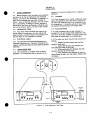
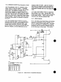
OVERALL BLOCK DIAGRAM DISCUSSION
4-2 The power supply, as shown on the overall
block diagram on Figure 4-1, consists of a power
transform er, a rectifiei -preregu lator-fil ter, preregulato r (SCR) control circuit, series regulato r,
error amplifie rs. gating circuit, a constan t voltage input circuit. a constant current input circuit,
a fault input circuit, a referenc e circuit, bias
supply, and a meter circuit.
•
4-4 The series regulato r. part of another feedback loop, is made to alter its conducti on to maintain a constant output voltage or current. Its conduction varies in accordan ce with feedback control
signals obtained from the error amplifier . It
should be noted that the series regulato r provides
fine and "fast" regulatio n of the output, while the
preregul ator handles large relativel y "slow" regulation demands . The de current from the series
regulato r passes through a current sampling resistor before reaching the positive output terminal .
4-3 The input line voltage is reduced to the
proper level by the power transform er and coupled
to a rectifier bridge consistin g of two rectifier
diodes and two SCR's. The bridge simultan eously
performs the necessa ry rectifyin g and preregu\ ating function s. The SCR's, oper~ting in conjunc tion with a control circuit, minimize the power
dissipate d by the series regulato r by keeping the
yoltage drop across the regulato r at a low and
constant level. The SCR control circuit accom-
4-1
PIO
-
-
.
~
.•
"
.
-•
IEFEllENCE
UGtll-'TOa
0600 THlU
0503
l"'
ctoo:::
I
.....--
2
CHOI
-
-•.zv
•9.fV
~
_ •6.2V
~
I
•YOLt!I
CllOO
u
•1~4V
CUlllENT
-
(NOU 2)
J
...
INPUT
CIRCUIT
'
0200
-s
l>-U
~
...
CIOO:
~
HO~
I
nNE
CUUENt/
cu:r...i :-:aot
-1.zv
.1
I TIOO
~-
PllllllVnoN
IUV DBI -
3
I
I
1903
TOFF -
I .
·~-,1
AC
Sl
~
"'
::
.
•...
••
ISO
CISO
~50
:
504
CISOI
2
ISOl
-
-
I
PIO
9
)
•
SCI
COlnlCL
ClllCU1T
0100.0101.
0102
rl
'10
Cl404,
- i
-
r. '?
TIO!
Al
-0
1827
.,. ,; i-
!5_0~
../
COMSE
Clt40l 1
Cltl02
: 1125
CllS02
4
smi:s
UGO
QG.
CUllU:NT
Q400IQ401)
:.~JIOnJ
•
•9.olV
llSIS101
•
-
"'
•U05
0303
GlllNG
ClllCVIT
0300.
0301
1111:·
.
AMU.
0102.
•
FAULT
UfPUT
CllCUlT
•· ·-- .QIDI
-
-
u
@
nm:
~814
YOLts,/.
ADJ.
"""2
CS09=
1.
VOLTAGE ACROSS CIOO rel &ACK MODEL IS SllOWJI IUDW1
MODEL NO.
'212A &USA '2t~ - 62IOA '211A 1216A
YOL1S CDC>
16. 2
11.2
16. 2
u.2
11.2
21.2
l.
l'OSITM lllAS VOLTAGE "FOR UCH MODEL l$ SHOWJll · IELOW:
MQPQ. NO.
6282" &285" &216A 129DA '291A 1216A
YOL1S (DC)
•lSV
•I 7V
•UV
•2DV
'17V
•ZDY
3.
VOLTAGE ACROSS INPUT FILD:a CAPACITOR FOR PCB MOmL
IS SHOWN IELOW:
6282"
IS
62 HA
U
Ul6A
24
i290A
4!>
l29U.
45
ADJ.
MftP ~
CllCUJT
0150 tlllt""
Ol5J,S2
•
·-·
. 1
.,~~:
=-,_,f802
-
llOLts ) :i:.13
{
,
,,
COMSE
r.7
NOTIS:
__
j
YOl.DGE
·INPUT
cac:UIT
0100
-
u
MQQEL NO.
YOLlS (DC)
~110
ADJ.
Cl!_80l
15
ACC
•
CHOO
TIOI 8
J
-s
.
~
uu.
'
J
.
-·
&ZHA
&S
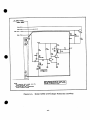
Fiqure 4-2. Simplified Schematic
•
4-2
•
4-S The feedback signals that control the conduction of the series regulator are originated within the constant voltage input circuit or the constant current input circuit. The output voltage of
the power supply is sampled by the constant voltage input circuit by means of the sensing terminals {:S). The voltage developed across the current sampling resistor is the input to the constant
current input circuit. This voltage drop varies in
direct proportion to the output current. Any
changes ·in output voltage/current are detected in
the constant voltage/constant current input circuit, amplified by the gating and error amplifiers,
and applied to the series regulator in the correct
phase and amplitude to counteract the changes.
•
DETAILED CIRCUIT ANALYSIS
4-11
PREREGUIATOR AND CONTROL CIRCUIT
4-12 The prere9ulator minimizes changes in the
power dissipated by the series regulator due to
output voltage or input line voltage changes.
Preregulation is accomplished by means of a phase
control circuit utilizing SCR's CRS04 and CRS02 as
the switching elements. The appropriate SCR is
fired once during each half-cycle (8.33 milliseconds) of the rectified ac (see Figure 4-3). Notice
that when the SCR is fired at an early point during
the half-cycle, the de level applied to the series
regulator is fairly high. When the SCR is fired
later during the cycle, the de level is relatively
low.
The fault input circuit detects the presence
4-6
of overvoltage or overcurrent conditic:>ns and generates the necessary tum-down signals to the
SCR control circuit or the series regulator circuit.
In the case of an overvoltage condition, a tumdown signal is applied to the SCR control circuit.
The series regulator receives a turn-down signal
via the gating circuit if an overcurrent condition
is detected.
•
4-10
60Hz AC INPUT
~
I
'
I
•
'-8. JMs-.:1
I
I
I
I
IAll~;c~ --~
I
The reference circuit provides stable refer4-7
ence voltages which are used by the constant
voltage/current input circuits for comparison pur•
poses. The bias supply furnishes voltages which
are used throughout the instrument for biasing
purposes. The meter circuit provides an indication of output voltage or current in one of two
ranges.
I
•
'
•
.
I
I
I EARLY
I rIRINC
I
I
I
SMALL DC __ :
LEVCL
I
I
'-.\
i
POINT
~I~:
.Y- - - ~ - - -~
\
/.
U.oER
4-8
rIRINC
POlllT
SIMPLIFIED SCHEMATIC
-Figure 4-3. SCR Phase Control of DC Input Level
A simplified schematic of the power supply
4-9
is shown in Figure 4-2. It shows the operating
controls; the ON-off pushbutton, the voltage programming controls (R813 and R814) and the current
programming controls (R809 and R810). The
METER switch, i-ncluded in the meter circuit block
on Figure 4-2, allows the meter to read output
voltage or current in one of two ranges. Figure
4-2 also shows the internal sources of bias and
reference voltages and their nominal magnitudes
with an input of 115 Vac and no load connected.
Diode CR809, connected across the output terminals of the power supply, is a protective device
which prevents internal damage that might occur if
a reverse voltage were applied across the output
terminals. Output capacitor, C809 stabilizes the
feedback loop when the normal strapping pattern
shown in Figure 4-2 is employed. Note that this
capacitor can be removed if an increas~ in the
programming speed is desired. Under these conditions, capacitor C802 serves to insure loop
stability. Resistors R811 and R812 limit the output of the supply if the straps between the output
and sensing terminals are inadvertently opened.
4-13 The SCR control circuit (See Figure 4-4)
samples the input line voltage, the output voltaQe,
and the voltage across the series transistor. It
generates a firing pulse, at the time required, to
fire the SCR so that the voltage across input
capacitor CSOO will be maintained at the desired
level.
4-14 The inputs to the control circuit are algebraically summed across capacitor C700. All inputs
contribute to the time required to charge C700.
The input line voltage is rectified by CR704 through
CR707, attenuated by voltage divider R700 and
: R701. and applied to the summing point at TP 59
via capacitor C700. Capacitor C701 is used for
smoothing purposes.
4-15 Transistor Q702, connected in a common
base configuration, provides a charging current
for the summing capacitor which varies in accordance with the input signals applied to its emitter.
4-3
H:IO -0
SERIE.;
REG.
"'~
-0
-0
+v
•V
R708
1710~
10
CJ
R707
Cll708
;iti=t~
-6.Zv
•V
~E
CRSQQ
R9QJ
•
4
CR902
SCll"S
0702
CR900
11
C700
SUMMING
CAPACJroR
R900
~I
~ :;~p
12
C70Z
R701
R705
•15. 4V
CR711 CR710
AJ>J.
C701
R706
R709
•6.2V
Figure 4-4.
SCR Control Circuit, Simplified Schematic
Resistor R713, connected between the negative
output line and the emitter of Q702, furnishes a
signal which is proportional to the output voltage.
Resistors R708 and R707 sample the voltage
across, and the current through, the series regulator. Capacitor C702 and resistor R709 stabilize the control circuit feedback loop. Resistors
R7ll and R712 are the source of a constant offset
current which sustains a net negative charging
current to the summing point, ensuring that the
SCR's will fire at low output voltages.
.--r
FIRING
TP59
SUMMING POINT
l:V
THR£5HOU>
I
- -~-.....:l
I
"'-8. lMS
TP47
OUTPUT 0700
~NOTE
3)
I
I
I
l
11
I
nn
;
'-1:-
:
TP46
l'llUNG PULSE
(EXPANDED)
I
,
'
I
c··-J
l' •
J_
I
I
TPSZ
RESET
l!iV
_J_
I
I
I
4-16 The summation of the input signals results
in the generation of a voltage waveform at TP 59
similar to that ~hewn on Figure 4-S. When the
linear ramp portion of the waveform reaches a
certain negative threshold voltage, diodes CR711
and CR710 become forward biased. The negative
voltage then is coupled to the base of transistor
Q701. Transistors Q701 and Q700 form a squaring
circuit resembling a Schmitt trigger configuration.
Q701 is conducting, prior to firing time, due to
·the positive bias connected to its base through
R705. Transistor Q700 is cut off at this time because its base is connected directly to the collector of conducting transistor Q701. When the negative threshold voltage is reached, transistor
Q701 is turned off which turns Q700 on. The
conduction of Q700 allows capacitor C703 to discharge rapidly through pulse transformer T700
resulting in the SCR firing pulse shown on the
•
----r
1911
--1.
NOTES;
l. ALL WAVEFORMS REFERENCED TO
INBOARD SIDE or CURRENT SAMPLING RESISTOR R800 EXCEPT
l'IRJNG PULSE WHICH IS REFEll·
ENCED TO T. P. 45.
2. FOR CLAllJTY WAVEFORMS ARE NOT
3.
DRAWN TO SCALE.
AMPLITUDE OF THIS WAVEFORM IS
APPROXIMATE ANO VAIUES SUGHTLY
l'ROM MODEL 'TO MODEL IN AC·
COROANCE WITH THE POSmvE
COLLECTOR BIAS OBTAINED FROM
caoo.
Figure 4-5. SCR Control Circuit Waveforms
4-4
•
•
·serves as the series, or "pass", element which
provides precise and rapid control of the output.
The conduction of the series translstor(s) ls controlled by the feedback signals obtained from
driver Q303. Diode CR400, connecteii across the
regulator circuit, protects the series element(s)
from reverse voltages that could develop ac.;ross
them during parallel operation if one supply is
turned on before the other.
diagram. The firing pulse ls. relatively narT"ow because Q700 saturates rapidly causing the magnetic
field surrounding T700 to collapse. Diode CRSOO
damps out the negative overshoot.
4-17 Reset of the control circuit occurs once
every 8.33 milliseconds when the rectified ac
voltage at test point 52 recedes to a level at
which diode CR709 becomes forward biased.
Summing capacitor C700 is then allowed to discharge through CR709. Diodes CR711 and CR710
become reverse biased at reset and transistor
Q701 reverts to its "on" state. Consequently,
Q700 is turned off and capacitor C703 charges up
through R703 at a comparatively slow rate until the
collector voltage of Q700 reaches approximately
+17 volts. The above action causes the small
negative spike that appears across the winding of
pulse transfonner T700 at reset time.
4-21 CONSTANT VOLTAGE INPUT CIRCUIT (See
FigurP 4-6)
4-22 The circuit consists of the programming resistors (RB13 and R814) and a differential amplifier
stage (QlOO and associated components). Transistor QlOO consists of two silicon transistors
housed in a single package. The transistors have
matched characteristics minimizing differential
voltages due to mismatched stages. Moreover,
drift due to thermal differentials ls minimized,
since both transistors operate at essentially the
same temperature.
4-18 Capacitor C900, diode CR900, and ~stor
R900 fonn a long time constant network which
achieves a slow tum-on characteristic . When the
unit is firSt turned on, C900 provides a positive
voltage to the cathode of CR71 l to ensure that lt
ls initially reverse biased. After C900 becomes
fully charged, the control circuit ls permitted to
fire the SCR's. Diode CR902 provides a discharge
path for C900 when the unit ls turned off.
•
4-19
4-23 The constant voltage input ctrcuit continuously compares a fixed reference voltage w 1th a
portl.On of the output voltage and, if a difference
exists, produces an error voltage whose amplitude
and phase is proportional to the difference. The
error output is fed back to the series regulator,
through the gating and error amplifiers. The error
voltage changes the conduction of the series
regulator which, in tum, alters the output voltage
SERIES REGUIATOR
4-20 The series regulator (transistor Q400 or
Q400 and Q401, see schematic at rear Of manual)
RIOOA
•6.ZV
+9.('i
10
.
~TING.__-+....,
ll07
CIUOZ _ _ _,.
__.,._
_
llOS
PU1.LOUT
CIRcurT
U:S.ISTCll
+U,4¥
ll03
RlO'
RlOI
-6.%V
R105
CIOl
•6.ZV
•
Figure 4-6. Constant Voltage Input Circuit, Simplified Schematic
4-S
uo•
so that the difference between the two input voltages applied to the differential amplifier is reduced to zero. This action maintains the output
voltage constant.
the programming resistors, increase the high
frequency gain of the input amplifier. Resistor
R806, shunting the pullout resistor, serve1s as a
trimming adjustment for the programming current• •
Diode CR102 establishes the proper collector bia
for QlOOA while R103 and ClOO proVide low frequency equalization for the feedback loop.
4-24 Stage QlOOA of the differential amplifier is
connected to a common (+S) potential through impedance equalizing resistor Rl06. Resistors Rl02
and Rl 08 are used to zero bias the input stage.
offsetting minor base to emitter voltage differences in QlOO. The base of QlOOB is connected
to a summing point (A4) at the junction of the programming resistors and the current pullout resistor RSOS. Instantaneous changes in the output
(due to load variations) or changes due to the
manipulation of RBl 3, result in an increase or
decrease in the summing point potential. 01008
is then made to conduct more or less, in accordance with summing point voltage change. The
change in QlOOB's conduction also varies the
conduction of Ql OOA due to the coupling effects of
the common emitter resistor, RIOS. The "errorn
voltage is taken from the collector of QlOOA and
ultimately varies the conduction of the series
regulator.
4-26 CONSTANT CURRENT INPUT CIRCUI'I' (See
Figure 4-7)
4-27 This circuit is similar in appearance and
operation to the constant voltage input circ:uit. It
consists of the coarse and fine current pr01;ramming resistors (R809 and RS! O), and a difforential
amplifier stage (Q200 and associated components).
Like transistor QlOO in the voltage input ciircuit,
Q200 consists of two transistors, having matched
characteristics, that are housed in a singl1~ package.
4-28 The constant current input circuit continuously compares a fixed reference voltage with the
voltage drop across the current sampling re:sistor.
If a difference exists, the differential amplifier
produces an "error" voltage which is propo1rtional
to this difference. The remaining components in
the feedback loop (amplifiers and series re·;ulator)
function to maintain the drop across the cu:rrent
sampling resistor, and consequently the output
current, at a constant value.
4-25 Resistor Rl04, in series with the base of
QlOOB. limits the current through the programming
resistors during rapid voltage tum-down. Diodes
CRlOO and CRlOl form a limiting network which
prevents excessive voltage excursions from over
driVing stage QlOOB. Capacitor C801, shunting
•
-i.2V
-r..zv
?O
---+--...
GATING--~-.....
ClllCUIT
1801
P11U.OVT
RESISTOR
ltl08
CIOS
-L2V
RIOOA
R827
Figure 4-7. Constant Current Input Circuit, Simplified Schematic
4-6
•
•
4-36 Capacitor C900, diode CR901, and resistor
R902 form a long time constant network which
achieves a slow tum-on characteristic. When the
unit is first turned on, C900 provides a positive
voltage to the base of Q302 keeping the series
regulator from conducting initially. As C900
charges up, the restrictive bias becomes less
positive enabling the regulator to conduct. Diode
CR902 provides a low resistance discharge path
for C900 when the unit is turned off.
4-29 Stage Q200A is connected to +S through impedance equalizing resistor R203. Instantaneous
changes in output current on the positive line are
felt at the current summing point (terminal A7) and,
hence, the base of Q200B. Stage Q200B varies its
conduction in accordance with the polarity of the
change at the summing point. The error voltage is
taken from the collector Q200B and ultimately
varies the conduction of the series regulator.
4-30 Resistor R304, in conjunction with C300,
helps stabilize the feedback loop. Resistor R808,
shunting the pullout resistor, serves as a trimming
adjustment for the programming current flowing
through R809 and R810.
4-31
•
4-37
4-38 The fault input circuit (see schematic at
rear) protects the power supply against overvoltage and overcurrent conditions. Transistor 0800,
and associated components, comprise the overvoltage detector. With normal output voltages
QSOO is cut off due to the +15.4V reference voltage
connected to the top of voltage divider R823 and
R821. If the output voltage exceeds a certain
limit (about 20% above the maximum rated output
voltage) transistor QSOO is driven into conduction.
Current is then conducted away from the summing
point and in opposition to the charge path of C700
in the SCR control circuit. As a result, the SCR' s
are fired at a later time, reducing the series regulator input voltage to a safe value.
GATING CIRCUIT
4-32 The gating circuit (see schematic) consists
of gating amplifiers Q301 and Q300 and associated
OR-gate diodes, CRJOO and CR301. The gating
circuit provides sharp crossover between constant
voltage and constant current operation. During
steady state conditions, one transistor is saturated while the other is conducting in its linear
region. The cathodes of the OR-gate diodes are
always at a more positive potential than the satuation potential of 0300 or Q301. Thus, the diode
associated with the saturated transistor is reverse
biased while the diode associated with the other
transistor is forward biased. In the constant voltage mode Q301 is operating in its linear region
and Q300 is saturated due to the positive collector
voltage of Q200B. OR-gate diode CR301 is therefore reverse biased while OR-gate diode CR300 is
forward biased, coupling the constant voltage
feedback si9nal to the error amplifier. Opposite
conditions prevail during constant current operation.
4-39 A full wave rectified voltage, obtained from
the SCR control circuit, excercises a stabilizing
influence on transistor QBOO. This signal tends
to synchronize the conduction of QBOO at a 120 Hz
rate preventing random firing of the SCR' s.
4-40 Transistors Q801 and Q802 provide overcurrent and short circuit protection for the unit.
Overcurrent protection is accomplished by Q802
which is activated only 1f the constant current
input circuit should fall. Q802 monitors the voltage drop across the current sampling resistor and
conducts if this drop exceeds a certain level.
The output of Q802 is fed to gating amplifier QJOl
via R815 and ultimately reduces the conduction of
the series regulator.
4-33 Capacitor C302 is a commutating capacitor
which improves the transient response of the unit.
Resistor R300 is the biasing resistor for the ORgate diodes.
4-34
ERROR AMPLIFIERS
4-41 Short circuit protection is provided by transistors Q801 and Q802. Transistor Q801, normally biased below cutoff, monitors the voltage drop
across the series regulator. Under short circuit
conditions, the ·increased voltage across the regulator drives Q801 into saturation. The positive
going emitter voltage of Q801 also drives Q802
into conduction. The output of Q802 limits the
current flow through the series regulator to a prescribed leve 1.
4-35 The error amplifiers Q302 and QJOJ, amplify the feedback. si9nal from the constant voltage
or constant current input circuit to a level sufficient to drive the series regulator transistor.
Transistor Q303 serves as the driver and Q302 the
predriver. for the series regulator. The RC network, composed of C301 and R307, is an equalizing network which provides for high frequency rolloff in the loop gain response in order to stabilize
the feedback loop .
•
FAULT INPUT CIRCUIT
4-7
4-42 REFERENCE CIRCUIT (See Schematic at Rear)
tected by Q602 and Q603. The error voltage is
amplified and inverted by Q601 and appli.ed to
series requlator Q600 in the correct phase and
amplitude to maintain the +15.4 volt output c o n .
stant.
4-43 The reference circuit is a feedback power
supply similar to the main supply. It provides
stable reference voltages which are used throughout the unit. The reference voltages are all
derived from smoothed de obtained from the full
wave rectifier (CR600 and CR601) and filter capacitor C600. The +9.4 and -6.2 voltages are developed across temperatu re compensa ted Zener diodes
VR600 and VR60l. Resistor R611 limits the current
through the Zener diodes to establish an optimum
bias level.
4-46
4-44 The regulating circuit consists of series
regulating transistor Q600, error ammplifie r Q601,
and differenti al amplifier Q602 and Q603. The
voltage across the Zener reference diode VR600
and the voltage at the junction of divider R605 and
R606 are compared, and any difference s are de-
4-47 The meter circuit (see Figure 4-8) provides
continuou s indication s of output voltage •lr current on a single multiple range meter. The meter
can be used either as a voltmeter or an ammeter
depending upon the position of METER switch S2
on the front panel of the supply. This SVl'itch
4-45 Zener diode VR601 provides an add:ltiona l
bias voltage of -6.2 volts. Resistor R60l, connected across Q600, minimiZes power di:;sipatio n
in the series element. Output capacitor C602
stabilizes the reference regulator loop.
METER CIRCUIT
1800
CtJRllENT
SAM PUNG
Rl:SJSTOR CSI
R853
R869
I
18SZ
•
RB62
RB61
11851
RB&O
R8'1
R872
QH2
R857
RISO
HOtt:
S2 FOSmoNS FOR I>IFFERENT MOI>EU
ARE SHOW?-! BELOW:
MODEL
628ZA
628;.\
6286A
629~A
6291.\
6Z96A
I
S2 TERl\.!TN& NOS.
2
3
4
l.2V
2. 4V
2.4V
12V
24V
Z4V
;v
sv.
;ov
sov
7V
70V
HA
6A
IZA
l.ZA
.6A
l.ZA
4A
6A
.4A
.6A
4A
.u.
Figure 4-8.
Meter Circuit. Simplified Schemati c
4-8
•
•
to stage Q851B while stage Q851A is grounded to
the +S terminal. In the low current range, the
voltage drop across R853 and R854 is applied to
Q851B.
also selects one of two meter ranges on each
scale. The metering circuit consists basically of
a selection circuit (switch S2 and associated
voltage dividers), a stable differential amplifier
staqe (QBSlA and Q8518), two meter amplifiers
(Q852 and Q853), and the meter movement.
Differential amplifier stage Q851 is a
stable device having a fixed gain of ten. To
minimize temperature effects, the two stages are
housed in a single package that is similar to
those used in the constant voltage and current input circuits. The outputs of the differential amplifier drive meter amplifiers Q852 and Q853
which, in turn, deflect the meter. Transistor
Q850 provides a constant bias current to the emitters of Q852 and Q853. Potentiometer R870 permits electrical zeroing of the meter.
4-49
4-48 The selection circuit determines which
voltage divider is connected to the differentia 1
amplifier inpu~. When S2 ls in one of the voltage
positions, the voltage across divider RBSO, RBSl.
and R852 (connected across the output of the supply) is the input to the differential amplifier.
When 52 is in one of the current positions, the
voltage across divider R853, R854, and RSSS (connected across the sampling resistor) is the input
to the differential amplifier. With S2 in the higher
voltage range (position 2) the voltage drop across
R852 is applied to stage Q851A while stage
Q851B is grounded tothe +s terminal. For low output voltages, S2 can be set to position (1) resulting in the application of a larger percentage of the
output voltage (drop across RSS l and RBS 2) to
stage Q851A. With 52 in the higher current position (3) the voltaqe drop across R853 is applied
4-50 The meter circuit contains an inherent current limiting feature which ~rotects the meter
movement against overloads. For example, lf
ME1'~R switch 52 is placed in the low current
range when the power supply is actually delivering a higher ampere output, the differential amplifiers are quickly driven into saturation, limiting the current through the meter to a safe value .
•
•
4-9
•
SECTION V
MAINTENANCE
5-1
INTRODUCTION
5-2 Upon receipt of the power supply, the performance check (Paragraph 5-10) should be made.
This check is suitable for incoming inspection. If
a fault is detected in the power supply while making
the performance check or during normal operation.
proceed to the troubleshooting procedures (Paragraph S-41). After troubleshooting and repair (Paragraph S-46), perform any necessary adjustments
and calibrations (Paragraph 5-48). Before returning
the power supply to normal operation, repeat the
performance check to ensure that the fault has been
properly corrected and that no other faults exist.
Before doing any maintenance checks, tum on power supply, allow a half-hourwarm-up, and read the
'general information regarding measurement techniques (Paragraph 5-3).
•
5-3
Figure 5-1. Front Panel Terminal Connections
tor. The four terminals are connected as shown in
Figure 5-2. In addition, the resistor should be of
the low noise, low temperature coefficient Oess
than 30ppmfOC) type and should be used at no
more than 5% of its rated power so that its temperature rise will be minimized.
GENERAL MEASUREMENT TECHNIQUES
5-4 The measuring device must-be connected
across the sensing leads of the supply or as close
to the output terminals as possible when measuring
the output impedance, transient response, regulation. or ripple of the power supply in order to
achieve valid measurements. A measurement made
across the load includes the impedance of the leads
to the load and such lead lengths can easily have
an impedance severa 1 orders of magnitude greater
than the supply impedance. thus invalidating the
measurement.
S-5 The monitoring device should be connected
to the +S and -s terminals (see Fic;ure 3-2) or as
shown in Figure S-1. The performance characteristics should never be measured on the front terminals
if the load is connected across the rear terminals.
Note that when measurements are made at the front
terminals. the monitoring leads are connected at A,
not B, as shown in Figure S-1. Failure to connect
the measuring device atA willresuitin a measurement that includes the rest.stance of the leads between the output terminals and the point of connection.
•
LOAD LEAD
CURRENT SAMPLING
TERMINALS
TO UNGROUNDED
TERMINAL OF
TO GROUNDED
+-W.--~W.."'0---1•
POWER SUPPLY
TERMINAL OF
POWER SUPPLY
Figure 5-2. Output Current Measurement Technique
5-7 When using an oscilloscope, ground one terminal of the power supply and then ground the case
of the oscilloscope to this same point. Make certain that the case is not also grounded by some
other means (Power line). Connect both oscillo. scope input leads to the power supply ground terminal and check that the oscilloscope is not exhibiting a ripple or transient due to ground loops, pickup, or other means.
s-e
TEST EQUIPMENT REQUIRED
S-9 Table 5-1 lists the test equipment required to
perform the various procedures described in this
Section.
S-6 For output current measurements, the current
sampling resistor should be a four-terminal rests-
5-1
Table 5-1. Test Equipment Required
Type
Require d
Charac teristic s
Recommended:
Model
Use
Differe ntial
Voltme ter
Sensitiv ity: 1 mv full scale
(min.J. Input impeda nce:
10 megohms (min.).
Measur e DC voltage s;
calibra tion procedu res
~ 3420 (See Note)
Variabl e
Voltage
Transfo nner
Range: 90-130 volts.
Equipped with voltmet er
accurat e within 1 volt.
Vary AC input
----------------
AC Voltmeter
Accuracy: 2%. Sensitiv ity:
1 mv full scale deflecti on
(min.).
Measur e AC voltage s and
ripple
~ 403 B
Oscillo scope
Sensitiv ity: 100 ~v/cm.
Differe ntial input.
Display transie nt respons e
wavefo rms
~
Oscilla tor
Range: SHz to l MHz.
Accuracy: 2%.
Impeda nce checks
e 200 CD
DC Voltme ter
Accuracy: 1%. Input
resistan ce: 20, 000 ohms/v olt
(mtn.l.
Measur e DC voltage s
~ 412A
Repetit ive
Load Switch
Rate: 60 - 400 Hz, 21'5eC
rise and fall time.
Measur e transie nt respons e
See Figure 5-7
Resisti ve
Loads
Value: See Paragra ph 5-14.
and Figure 5-4. ::1:5% 250 watts.
Power supply load resistor s
-------------··--
Current
Samplin g
Resisto r
Value: See Figure 5-4.
111. 200 watts, 20ppm.
4-Term inal.
Measur e current : calibra te
meter
Resisto r
l'Kt.. ::1:1%. 2 watt non-ind uctive
Measur e impeda nce
----------------
Resisto r
100 ohms. i:S%. 10 watt
Measur e impeda nce
-------------··--
Value: See Paragra ph 5-45.
Calibra te programming current
-------------··--
Resisto r
•
140 A plus
1400A plug in.
•
-------------·---
:tO. 1%. 20 watt.
5-2
•
•
Recommended
Model
Type
Required
Characteristic s
Resistor
Value: See Paragraph 5-47.
:t:O. 1 %. l/2 watt.
Calibrate programming current
----------------
Capacitor
500µ.f, 50 wvdc
Measure impedance.
----------------
Decade
Resistance
Box
Range: 0-SOOK.
Accuracy: 0. 1% plus l ohm
Make-before-b reak contacts.
Measure programming
coefficients.
----------------
Use
NOTE
A satisfactory substitute for a differential voltmeter
is to arrange a reference voltage source and null
detector as shown in Figure S-3. The reference
voltage source is adjusted so that the voltage difference between the supply being measured and the
reference voltage will have the required resolution
for the measurement being made. The voltage difference will be a function of the null detector that is
used, Examples of satisfactory null detectors are:
S 419 A null detector, a DC coupled oscilloscope
utilizing differential input, or a SO mv meter movement with a 100 division scale. For the latter, a
2 mv change in voltage will result in a meter deflection of four divisions.
•
CAUTION
Care must be exercised when using an electronic
null detector in which one input terminal is grounded
to avoid ground loops and circulating currents.
REfUENCt
POWtR SUPPLY
VOLTAGE
SOURCE
UNDER TEST
S-10 PERFORMANCE TEST
5-11 The following test can be used as an incoming inspection check and appropriate portions
of the test can be repeated either to check the
operation of the instrument after repairs or for
periodic maintenance tests. The tests are per
fonned using a 115-VAC 60 cps., single phase input power source. If the correct result is not obtained for a particular check, do not adjust any
controls; proceed to troubleshootin g (Paragraph
5-28) •
0
LOAD
NllU. "DETECTOR
•
Figure 5-3.
Differential Voltmeter Substitute,
Test Setup
S-3
5-12 CONSTANT VOLTAGE TESTS
5-13 Rated Output and Meter Accuracy.
POWER SUPPLY
5-14 Voltage.
UNDER ?£ST
Proceed as follows:
MODEL NO.
a. Connect load resistor across rear output
terminals of supply. Resistor value to be as follows:
Model 6282A 628SA 6286A 6290A 6291A 6296A
Res.
1"'.
4A
~
llA
~
20~
b. Connect differential voltmeter across +S
and -s terminals of supply observing correct polarity.
c. Set METER switch to highest voltage range
and turn on supply.
d. Adjust VOLTAGE controls until front panel
meter indicates exactly the maximum rated output
voltage.
e. Differential voltmeter should indicate
maximum rated output voltage within :t2%.
5-15 Current.
a. Connect test setup shown in Figure 5-4,
leaving switch S l open.
b. Tum CURRENT controls fully clockwise.
c. Set METER switch to highest current range
and turn on supply.
d. Adjust VOLTAGE controls until front panel
m~ter indicates exactly the maximum rated output
current.
e. Differential voltmeter should read 1. 0 z
O. 02 Vdc.
1. 9
POWER Sll~Pl.Y
UNDER TEST
6286A
6289A
6290A
6291A
6294A
6296A
6299A
0. 20
0. JO
0. l3
0. 20
0. 10
0. 66
0. 33
0. 20
I. 0
0. 33
I. 33
I. 30
zi
13
7. 80
59
19. 66
131
OtrrtRENTIAL
VOLTMETER
Load Regulation, Constant Voltc:1ge
d. Adjust VOLTAGE controls until front panel
meter indicates exactly the maximum rated output
voltage.
e. Read and record voltage indicated on
differential voltmeter.
f. Disconnect load resistors·.
g. Reading on differential voltmeter should •
not vary from reading recorded in step e by more
than the following (variations expressed in mV"dc):
Model
6282A 6285A 6286A 6290A 6291A 64!96A
Variation :t2
:3
:1:3
:1:5
:5
:t7
5-17 Line Regulation. l'o check the line regullation, proceed as follows:
OIFrtllENTlAL
VOL?MCTER
RESISTOR
a. Connect variable auto transformer between
input power source and power supply power input.
b. Turn CURRENT controls fully clockwise.
c. Connect test setup shown in Figure s-s.
d. Adjust variable auto transformer for 105
VAC input.
e. Set METER switch to highest voltage
range and turn on supply.
f. Adjust VOLTAGE controls until front panel
meter indicates exactly the maximum rated output
voltage.
g. Read and record voltage indicated on. differential voltmeter.
•
h. Adjust variable auto transforn:ier for l.25
VAC input.
Figure· 5-4. Output Current Test Setup
S-16 Load Regulation. To check constant voltage
load regulation, proceed as follows:
a. Connect test setup as shown in Figure 5-5.
b. Turn CURRENT controls fully clockwise.
c. Set METER switch to highest current
range and turn on supply.
S-4
•
0. 90
6
3. 80
I. 90
If measurements are made at the front
terminals, readings will be O.SmV per
amp greater due to front terminal resistance.
ll
?. 8
19 66
SAM PUNG
6281A
6282A
6284A
6285A
R
NOTE
0. 90
l. 8
CURRCNT
R
Figure S-5.
Proceed as follows:
I
•
POWtR SUPPLY
UNDER TEST
i. Reading on differential voltmeter should
not vary from reading recorded in step g by more
than the following (variations expressed in mVdc):
Model
6282A 628SA 6286A 6290A 6291A 6296.A
Variation :2
:±3
:1:3
:5
±5
:7
0
5-18 Ripple and Noise. To check the ripple and
noise, proceed as follows:
OSCILLOSCOPE
,, 140A
+
0-+--------------------1-.0
CONTACT PROTECTION
Ntl'WORIC
l..ld
I" SW
200V
(NOTE 31
G
0
Ry
Rx
f----·Vlll.--..l\/V\.--1
a. Retain test setup used for previous line
regulation test except connect AC voltmeter across
output terminals as shown in Figure 5-6.
b. Adjust variable auto transformer for 125
VAC input.
c. Set METER switch to highest current range.
d. Turn CURRENT controls fully clockwise
and adjust VOLTAGE controls until front panel meter
indicates exactly the maximum rated output voltage.
e. AC voltmeter should read less than
O. 50mVrms.
.,
I
NOTES:
I. THIS DRAWING SHOWS
A SVCGESTED METHOD
or BUILDING A L~D
SWITCH. HOWMR.
OTHER METHODS COULD
IE USED: SUCH AS A
TRANSISTOR SWITCHING
NETWORK. MAXIMUM
LOAD RAnNGS or LOAD
SWITCH ARE; S AMPS.
SOOV. ZSOW INOT 2S0'1Wl
2. USE MERCURY REIAY:
CURE TYPE HGP I 002 OR
W. E. TYPE 2768.
l. USE Wtat WOUND
~ODEL NO.
6282A
628SA
6286A
6290A
6291A
6296"
POWER SUPPLY
UNDER 'ltST
RESIS A~·
Rx
0.10
0.20
0.10
0. 33
0.20
0. 33
RC.~ISTOR.
•~u~••
a.,
I
0.90
3. 80
1.90
13. 0
7. 80
1'. 66
Figure S-7. Transient Response, Test Setup
•
f. Adjust 2SK potentiometer until a stable
dis play is Qbtained on oscilloscope. Waveform
should be within the tolerances shown in Figure S-8
(output should return to within 15 mV of original
value in less than 50 microseconds).
LOAO RtSISTORS
AC VOLTMma
,, 403 •
f---so....~
J__
I
ISMV
I
ov-r-----__,,,c....____,i;;:::;::;._-r--
Figure S-6.
Ripple and Noise. Constant Voltage
5-19 Transient Recovery Time. To check the
transient recovery time proceed as follows:
I
1-so..stc-t
a. Connect test setup shown in Figure 5-7.
b. Turn CURRENT controls fully clockwise.
c. Set METER switch to highest current
range and turn on supply•
. d. Adjust VOLTAGE ~ontrols until front panel
meter indicates exactly the maximum rated output
current or S amperes, whichever is smaller.
e. Close line switch on repetitive load
switch setup.
UNLOADING TRANSIENT
~DING
TRANSIENT
Figure 5-8. Transient Response Waveforms
_:s-20 Output Impedance.
To check the output impedance, proceed as follows:
a. Connect test setup shown in Figure S-9 •
•
5-5
VOLTMEltR
INDICATES E;n
~
) (>
0
POWER SUPPLY
~/
0
5-23 Line Regulation. To check the line regulation, proceed as follows:
OSCIUATOR
ft 200 CD
UNDER TtsT
/
f. Short out load resistor (Ry) by closj.ng
switch Sl.
g. Reading on differential voltmeter should
not vary from reading recorded in step e by more
than the following {variations expressed in mVdc): •
6282A 628SA 6286A 6290A 6291A li296A
Model
Variation :1.:0. 60 :1:2. 20 :1.:0. 60 :t0.830 :t0.70 :1::0.830
VOLTMmlt
40) I
Ir
Ip 40) B
INDICATES E0
-
....
.__ ~+c
h
I
'J\11."v
..!IC.
SQO MrD
\I
-11+
a. Utilize test setup shown in Fiqure 5-4
leaving switch Sl open throughout test.
b. Connect variable auto transformer b1!tween
input power source and power supply power input. .. ·: ·
c. Adjust auto transformer for lOSVAC input.
d. Turn VOLTAGE controls fully clockwise.
e. Set METER switch to highest current range
and tum on supply.
f. Adjust CURRENT controls unW front panel
meter reads exactly the maximum rated output current.
g. Read and record voltage indicated (Jn differential voltmeter.
h. Adjust variable auto transformer fo1~ 125
VAC input.
i. Reading on differential voltmeter sltlould
not vary from reading recorded in step 9 by more
than the following {variations expressed in mVdc):
6282A 628SA 6286A 6290A 6291A 6296A
Model
Variation :1:0.60 :1:2.20 :t0.60 :t0.830 :tQ.70 :i:0.830
H U>
I
100 OHM
Figure S-9.
Output Impedance, Test Setup
b. Set METER switch to highest voltage range
turn CURRENT controls fully clockwise, and turn on
supply.
c. Adjust VOLTAGE controls until front panel
meter reads 10 volts.
d. Set AMPLITUDE control on Oscillator to
10 volts (Ein>. and FREQUENCY control to lOOHz.
e. Record voltage across output terminals of
the power supply (Eo) as indicated on AC voltmeter.
f. Calculate the output impedance by the
following formula:
EoR
5-24 Ripple and Noise. To
noise, proceed as follows:
Zout = Ein - Eo
Eo =nns voltage across power supply output
terminals.
R =1000
Ein= 10 volts
chec~ the ripple' and
•
a. Use test setup shown in Figure 5-<I. except connect AC voltmeter across sampling resistor
instead of differential voltmeter.
b. Rotate VOLTAGE controls fully cloc:kwise.
c. Set METER switch to highest currei~t range
and turn on supply.
d. Adjust CURRENT controls until front panel
meter indicates exactly the maximum rated output
current.
e. Turn range switch on AC voltmeter to lmV
position.
f. The AC voltmeter should read as f<>llows:
{Readings are expressed in mVac)
6282A 628SA 6286A 6290A 6291A li296A
Model
1. 0
0. 6
1. 0
Reading O.SO 0.60 0.50
g. The output impedance (Zout> should be
less than 0.001 ohm.
h. Using formula of step f, calculate output
impedance at frequencies of lKHz, lOOKHz, and
lMHz. Values should be less than 0.01 ohm, 0.2
ohm, and 2 ohms, respectively.
S-21 CONSTANT CURRENT TESTS
S-22 Load Regulation. To check the constant current load regulation, proceed as follows:
a. Connect test setup shown in Figure 5-4.
b. Turn VOLTAGE controls fully clockwise.
c. Set METER switch to highest current
range and turn on supply.
d. Adjust CURRENT controls until front panel
meter reads exacUy the maximum rated output current.
e. Read and record voltage indicated on differential voltmeter.
S-6
S-25 TROUBLESHOOTING
S-26 Components within Hewlett-Packard power
supplies are conservatively operated to provide
maximum reliability. In spite of this, parts within a supply may fail: Usually the instrument must
be immediately repaired with a minimum of "down
time" and a systematic approach as outlined in
succeeding paragraphs can greatly simplify and •
speed up the repair.
5-27 TROUBLE ANALYSIS
•
·a. Reference circuit check (Paragraph 5-31).
This circuit provides critical operating voltages fa
the supply and faults in the circuit could affect the
overall operation in many ways. This circuit should
be checked first, before proceeding to other areas
of the unit.
b. Series regulator and preregulator feedback
loop checks (Paragraph 5-32).
c. Procedures for dealing with common
troubles (Paragraph S-33}.
5-28 General. Before attempting to trouble shoot
this instrument, ensure that the fault is with the
instrument and not with an associated circuit.
The performance test (Paragraph 5-10) enables this
to be determined without having to remove the instrument from the cabinet.
5-29 Once it is determined that the power supply
is at fault, check for obvious troubles such as
open fuse, a defective power cable, or an input
power failure. Next, remove the top and bottom
covers (each held by four retaining screws) and
inspect for open connections, charred components,
etc. If the trouble source cannot be detected by
visual inspection, follow the detailed procedure
outlined in succeeding paragraphs. Once the defective component has been located (by means of
visual inspection or trouble analysis) correct it
and re-conduct the performance test. If a component is replaced, refer to the repair and replacement arxi adjustment and calibration paragraphs in
this section.
•
a. Make an ohmmeter check to be certain
that neither the positive nor negative output terminal is grounded.
b. Turn front-panel VOLTAGE and CURRENT
controls fully clockwise (maximum).
c. Turn on power supply (no load connected).
d. Proceed as instructed in Table 5-2.
5-32 Series Regulator and Prerequlator Feedback
Circuits. GenerallY> malfunction of these two feedback circuits is indicated by high or lQw (or no)
output voltage. If one of these situations occur,
disconnect the load and proceed as instructed in
Table 5-3 or 5-4. Preregulator waveforms are included on the schematic at the rear of the manual.
S-30 A good understanding of the principles of
operation is a helpful aid in troubleshooting, and
it is recommended that the reader review Section IV
of the manual before attempting to troubleshoot the
unit in detail. Once the principles of operation are
understood, logical application of this knowledge
used in conjunction with the normal voltage readings
and wavefcrms shown on the schematic and the additional procedures given in the following paragraphs should suffice to isolate a fault to a compo.-ient or small group of components. The component
location diagram at the rear of the manual can be
consulted to determine the location of components
and test points. The normal voltages shown on the
schematic are positioned adjacent to the applicable
test points (identified by encircled numbers on the
schematic and component location diagram). Additional test procedures that will aid in isolating
troubles are as follows:
Table 5-2.
5-33 Common Troubles. Table 5-6 lists the
symptoms, checks, and probable causes for common troubles.
S-34 REPAIR AND REPLACEMENT
5-35 Before servicing a printed wiring board, refer
to Figure 5-10. Section VI of this manual contains
a list of replaceable parts. Before replacing a
semiconductor device, refer to Table 5-7 which
lists the special characteristics of selected semiconductors. If the device to be replaced is not
listed in Table 5-7, the standard manufacturers
part number listed in Section VI is applicable.
After replacing a semiconductor device, refer to
Table 5-8 for checks and adjustments that may be
necessary.
Reference Circuit Troubleshooting
Step
Meter
Common
Meter
Positive
Normal
Indication
1
+S
29
9. 4 %0. 4Vdc
Check 15. 4 volt bias or VR600
2
28
+S
6. 2 +O. 3Vdc
Check diode VR601
30
15. 4 +o. 5Vdc
Check R605, Q600 through Q603, C600, CR600
and CR601 •
3
•
5-31 Reference Circuit.
+s
If Indication Abnormal. Take This Action
S-7
Table 5-3.
Step
1
Hi9h Output Volta9e Troubles hooting
Measure
Respons e
Voltage between TP26 and TP90
Probable Cause
a. OV or negative
a.
0400(04 01) shorted
CR400 shorted
b. More positive th-an
b.
0303 open or R309 shorted
Proceed to Step 2
a. OV to +O. 8V
a.
Open strap A3-A4
R813 or R814 open
R805 or R806 shorted
b. More negative than
ov
b.
Proceed to Step 3
More positive than
+l. 5V
a.
01008 shorted
OlOOA open
b. +o. 9V to +1. 5V
b.
Proceed to Step 4
a. More negative than
ov
a.
0302 open
0301 open
R30S. R300 shorted
ov
2
3
4
Voltage between +s and A4
Voltage between +S and 11
Voltage between +s and 21
Table 5-4.
Step
1
a.
Low Output Voltage Troubles hooting
Measure
Voltage between TP26 and TP90
Respons e
Voltage between TP90 and TP27
Proceed to Step 2
b. OV or negative
b.
Proceed to Step 3
a. Less positive than
a.
Chee le fuse Fl. If blow111
check CRS02 or CRS04 for
short. If not blown, proceed to Table s-s.
b. More positive than
b.
0400 (0401) open
Proceed to Step 3
a. Normal output
voltage
a. Constan t Current circuit
b. Low output voltage
b. If supply is furnishin g current without load, check
CR809, C802, or C803 fc>r
short. If it is not, proceed
to Step 3
a. More negative
than OV
a.
+sv
4
Disable Q200 by disconn ecting CR200
Voltage between +S and A4
Probable Cause
a.
+4V
3
I
a. More positive than
ov
2
•
5-8
•
faulty; check 02008,
R810. R809, for short.
Open strap A4-AS
R813, R814, C801
Proceed to Step 5
•
Table 5-4. Low Output Voltage Troubleshoo ting (Continued)
•
Step
s
+s
Voltage between
a.
and 11
b,
Table S-5.
Step
a. QlOOB open
+O. 9V to +l. SV
b.
QlOOA shorted
Q802 or Q80l shoned
Proceed to Step 6
a. Q303 shorted
0302 shorted
R3 l O shorted
Preregulato r/Control Circuit Troubleshoo ting
Probable Cause
Response
Measure
Waveform between 4 and 3 of
T700
l
Less positive than
+0.9V
a. OV or positive
Voltage between +s and 21
6
Probable Cause
Response
Measure
a.
Normal firing pulse
b. No or abnormal fir-
a.
b. T700 open
CRSOO shorted
Proceed to Step 2
ing pulse
•
2
3
Waveform between 90 and 47
a. Zero or small posi-
Waveform between 90 and 52
Q7 00 shorted
C703 shorted
Q701 open
R703, primary T700 open
Proceed to Step 3
b. +16 to +20 Volt level
b. Q700 open
c. Waveform distorted
R703 shorted
Q70l shoned
Proceed to Step 3
c. Proceed to Step 3
a. Amplitude incorrect
a.
Q702 defective
R707,R708, R713 incorrect value or open
C700, CR710, C711 defective
Period incorrect
b.
CR709 defective
Proceed to Step 4
a. Amplitude incorrect
a.
CR708, CR709, R702 defective
b. Period incorrect
b. CR700 through CR703
b.
4
a.
tive voltage
Waveform between 90 and 59
CRS02-CRS04 defective
R50l-RS02 open
CRSOl, CR503, T800
defective
defective
s
•
Waveform between 90 and 54
R700, R701, C701 defective
a. Amplitude incorrect
a.
b. Period incorrect
b • CR704 throuqh CR707 defective
5-9
Table 5-6. Common Troubles
Symptom
Checks and Probable Causes
a. Check operating setup for ground loops,
b. If output floating, connect 1 µ.f capacitor between output and ground
c. Ensure that supply is not crossing over to constant current mode
under loaded condition s.
d. Check for low voltage across CSOO or Q400.
e. Check for excessive ripple on reference voltages. Peak-to-p eak
ripple should be less than 2mV for +9. 4V and -6. 2V and less than
4mV for +15. 4V.
High ripple
Poor line regulation
a.
Poor load regulation
(Constan t Voltage)
a. Measurem ent technique . (Paragraph 5-16.)
b. Check reference circuit (Paragraph 5-31).
c. Ensure that supply is not going into current limit. Check consta.nt
current input circuit.
Poor load regulation
(Constan t Current)
b. C802, C803, and CR809 leaky,
Check reference circuit (Paragraph 5-31).
a. Check reference circuit (Paragraph 5-31).
c. Ensure that supply is not crossing over to constant voltage operation. Check constant voltage input circuit.
Oscillate s (Constant
Voltage I Constant
Current)
a. Check C301 for open, adjustmen t of R307 (Paragraph 5-50).
b. Check Rl03, ClOO or R304, C300.
Poor Stability
(Constan t Voltage)
a. Check reference voltages (Paragrap h 5-31).
b. Noisy programming resistors R813, R814.
c. CR100, CRlOl leaky.
d. Check Rl04, R805, R806, CS 0 l for noise or drift.
e • Stage QlOO defective .
..
Poor Stability
(Constant Current)
•
a.
b.
c.
d.
e.
Check reference voltages (Paragraph 5-31).
Noisy programming resistors R809, R81 o.
CR809, C803, C802 leaky.
Check R807, R808, R200, R800, for noise or drift.
Stage Q200 defective .
•
Table 5-7. Selected Semicond uctor Character istics
Reference
Designato r
Character istics
~ Stock No.
QlOO, Q200
Matched differenti al amplifier. NPN Si Planar. 70 (min.)
hFE IC= 1 mA. VcE = 5V.
Ico 0.01 µ.a @Vcbo = SV.
1854-022 9
2N2917 G. E.
@ le = 4A. VcE
NPN power. hFE = 35 (min);
= 4V.
1854-022 5
2N3055 R. C. A.
Matched differenti al amplifier.
NPN Si.
1854-0221
2N4045 Union Carbide
Q303. Q400
(Q401)
Q851
5-10
Suggested
Replacem ent
•
Table 5-7.
•
Selected Semiconductor Characteristics (Continued)
CR100-CR102,
CR200, CR300, CR301.
CRSOO, CR700, CR701
Si diode, 200 mA. 200 prv
1901-0033
1N48SB Sylvania
CR402. CR602,
CR803-CR806
Si Stabistor. 200 mA. 15 prv
1901-0461
1N4828 G. E.
VR300
Zener diode, 4. 22V, :!:5%
400 mw
1902-3070
1N749
Table 5-B.
Checks and Adjustments After Replacement of Semiconductor Devices
Function
Reference
•
•
Motorola
Adjust
Check
0100
Constant voltage differential amplifier
Constant voltage (CV)
line and load ~egu lation.
0200
Constant current differential amplifier
Constant ct:trrent (CC)
line and load regulation.
0300
Constant Current gating amplifier
CC load regulation.
Q301
Constant Voltage gating amplifier
CV load regulation.
0302. 0303
Error amplifiers
CV/CC load regulation
Transient response
0400 (0401)
Series Regulator
CV/CC load regulation
0600, Q601.
0602, Q603
Reference regulator
Reference ~oltages.
Overvoltage trip point.
0700, Q701
0702
SCR control
Voltage across
series regulator
R711
0851, 0852.
QBS3
Meter amplifiers
Meter zero. Voltmeter/
Ammeter tracking
R870,RB65,
RBSS
QBOl, QB02
Overcurrent detectors
Short output, ensure
that output goes to
zero without damage
to series regulator.
CRlOO, CRlOl
Limiting diodes
CV load regulation
CR403, CR404
Forward bias regulator
Voltage across each
diode O. 6 to O. 9 volts.
CR700-CR703
Rectifier bridge
Waveform between 52
and 90
CR704-CR707
Rectifier bridge
Waveform
and 90
5-11
b~tween
54
R307
R604
Excessiv e heat or pressure can lift the copper strip from the board. Avoid damage by using a
low power soldering iron ( 50 watts maximum) and following these instructio ns. Copper that lifts
off the board should be cemented in place with a qUick drying acetate base cement bavtng
good
electrica l insulating propertie s.
A break in the copper should be repaired by soldering a short length of tinned copper wire
across the break.
•
Use only high quality rosin core solder when repairing etched circuit boards. NEVER
USE
PASTE FLUX. After soldering , clean off any excess flux and coat the repaired area With a
high quality electrica l varnish or lacquer.
When replacing components with multJple mowiting pins such as tube sockets, electroly tic capacitors, and potentiom eters, it Will be necessary to lift each pin slightly, working around the
components several times unW it is free.
WARNING : If the specific instructio ns outlined in the steps below regarding etched circUit
boards
wlthout eyelets are not followed, extensive damage to the etched circuit board will result.
1. Apply heat sparingly to lead of component
to be replaced. If lead of component passes
through an eyelet
in the circuit
~- · .··
board, apply
heat on com- ~
ponent side ,.,,-~~~;__,
of board. If I.
lead of com-\:;
ponent does
not pass
--uirough an
eyelet, apply beat to conductor side of board.
2. Reheat solder in vacant eyeletand quickly
insert a small awl to cleaninsi de of hole.
If hole does
not bavi"iii
eyelet, insert awl or
a 157 drill
from conductor side _ _ _ _ _ _ _.....,
of board.
4. Boldpart againstbo ard(avoid overheati ng)
3. Bend clean tinned lead on new part and
and solder leads.
Apply heat to companent leads on correct
side af board
as explained
in step 1.
carefully insert
through eye lets or
holes in board.
C'''''''''''Up;Q!Q ~
•
In the event that either the circuit board has been damagedorthe conventional methodis impractical, use method shown below. This is especially applicable for circuit boards without eyelets.
1•. Clip lead as shown below.
2. Bend prcitrudlng leads upward. Bend lead
of new
APPLY
component SOLDER
around protruding lead.
Apply solder
using a pair
of long nose pliers as a heat sink.
This procedur e is used in the field only as an alternate m•?ans of repair. It is not used within
the factory.
Figure 5-10. Servicing Printed Wiring Boaf'!is
S-12
••
Table 5-8. Checks and Adjustments After Replacement of Semiconductor Devices (Continued)
•
CR600, CR601,
CRBOO, CRBOl,
CRS01-CRS04
Rectifier diodes
.Voltage across appropriate filter capacitor
VR600, VR601
Reference voltages
Check +9. 4V and -6. 2V
reference voltages
Table 5-9. Calibration Adjustment Summary
Adjustment or Calibration
•
Paragraph
Meter Zero
5-38
Pointer
Voltmeter Tracking
5-40
R870 and R865
Ammeter Trac king
5-42
R855
•voltage" Programming Current
S-44
.R806
•current" Programming Current
5-46
R808
Overvoltage Trip
5·48
R604
Transient Response
s-so
R307
Preregulator Tracking
5-52
R7ll
S-36 ADJUSTMENT AND CALIBRATION
S-37 Adjustment and calibration may be req\lired
after performance testing, troubleshooting, or repair
and replacement. Perform only those adjustments
that affect the operation of the faulty circuit and no
others. Table S-9 summarizes the adjustments arid
calibrations contained in the following paraqraphs.
5-38 METER ZERO
S-39 Proceed as follows to zero meter:
a. Tum off instrument (after it has reached
normal operating temperature) and allow 30 seconds
for all capacitors to discharge.
b. Insert sharp pointed object (pen point or
awl) into the small indentation near top of round
black plastic disc located directly below meter face.
c. Rotate plastic disc clockwise (cw) until
meter reads zero, then rotate ccw slightly in order
to free adjustment screw from meter suspension. If
pointer moves, repeat steps band c.
•
Control Device
5-40 VOLTMETER TRACKING
S-41 l'o calibrate voltmeter tracking, p-oceed as
follows:
S-13
a. To electrically zero meter, set METER
sWitch to highest current position and, With supply
off and no load connected, adjust R870 until front
panel meter reads zero.
b. Connect differential voltmeter across supply, obs Erving correct polarity.
c. Set METER switch to highest voltage range
and turn on supply. Adjust VOLTAGE control until
differential voltmeter reads exactly the maximum
rated output voltage.
d. Adjust R865 until front panel meter also
indicates maximum rated output voltage.
S-42 AMMETER TRACKING
5-43 To calibrate ammeter tracking, proceed as
follows:
a. Zero meter as described in step a of 5-41.
Connect test setup shown on Figure 5-4 leaving
switch Sl open.
b. Turn VOLTAGE control fully clockwise and
set METER switch to hiqhest current range.
c. Turn on supply and adjust CURRENT controls until differential voltmeter reads 1. OVdc.
d. Adjust R855 until front panel meter indicates exactly the maximum rated output current.
5-44 CONSTANT VOLTAGE PROGRAMMING CURRENT
5-45 To calibrate the constant voltage programming
current, proceed as follows:
a. Connect a 0. l % , 20 watt resistor between
terminals -S and A4 on rear barrier strip. Resistor
value to be as follows:
Model 6282A 6285A 6286A .6290A 6291A 6296A
Res.
2K
4K
4K
SK
BK
l 8K
b. Disconnect jumper between A3 and A4 on
rear terminal barrier strip.
c. Connect a decade resistance in place of
R806.
d. Connect a differential voltmeter between
+S and -S and turn on supply.
e. Adjust decade resistance box so that differential voltmeter indicates maximum rated output
voltage within the following tolerances:
Model
6282A 6285A 6286A 6290A 6291A 6296A
Tol.(Vdc) :0.2 ::i:0.4 ::t.:0.4 ::t.:0.8 :0.8 ::i:l.2
f. Replace decade resistance with resistor
of appropriate value in R806 position.
5-46 CONSTANT CURRENT PROGRAMMING
CURRENT
5-47 To calibrate the constant current programming
current, proceed as follows:
a. Connect power supply as shown in Fig. 5-4.
b. Remove strap between A6 and A7 (leaving
A7 and AS jumpered).
c. Connect a O. 1 % , 1/2 watt resistor between Al and A7. Resistor value is l!V. (1. SKt. for
Models 6290A and 6296A).
d. Connect decade resistance box in place
of R808.
e. Set METER switch to highest current
range and turn on supply.
f. Adjust the decade resistance so that the
differential voltmeter indicates 1. 0 ::1: O. 02Vdc.
g. Replace decade resistance with appropriate value resistor in R808 position.
5-48 OVERVOLtAGE TRIP
5-49 To adjust the overvoltage trip point, proceed
as follows:
a. Connect differential voltmeter acres s +S
and -S terminals of supply.
b. Rotate VOLTAGE controls fully clockwise.
c. Turn on unit. Differential voltmeter
should read 20% above maximum rated output voltage within :!:5%.
d. If it does not, turn off supply and connect
decade resistance across R60S in place of R604.
e. Adjust decade resistance until differential
voltmeter reads that indicated in step c.
NOTE
The +15.4V reference voltage must
be kept within ::i:0.5Vdc when adjusting the decade resistance box.
5-14
f. Replace decade resistance With r•esistor
of appropriate value in R604 position.
5-50 TRANSIENT RECOVERY TIME
S-51 To adjust the transient response, proceed a .
follows:
a. Connect test setup as shown in Figure 5-7.
b. Repeat steps a through e as outlined in
Paragraph 5-19.
c. Adjust R307 so that the transient response
is as shown in Figure 5-8.
5-52 PREREGULATOR TRACKING (60Hz OPERATION)
5-53 To adjust the preregulator control circ:uit with
a 60Hz ac input, proceed as follows:
a. Connect proper load resistor acroiss output terminals of supply. Resistance value 1to be as
follows:
MQQfil. 6282A 6285A 6286A 6290A 6291A 6296A
Res.
l.n.
4n.
2.n.
l 3n.
8.n.
2o.,..
b. Connect DC voltmeter between TP27 and
TP90 (across series regulator).
c. Turn on supply and adjust VOLTAGIE controls for maximum rated output voltage.
d. Adjust i71 l so that DC voltmeter reads
3 ::i: O. 2Vdc.
5-54 PREREGUIATOR TRACKING (SOHz OPERATION)
5-55 To adjust the preregulatorcontrol circuitwhe.n
the ac input is from a SOHz source, proceed as
follows:
a. Connect load resistor across rear output
terminal of supply. Resistor value to be as follows:
Model 6282A 6285A 6286A 6290A 6291A 6296A
Res.
l.n.
4n
2.n.
l 3n.
Sn
20.n.
b. Connect o.scilloscope (de coupled) across
series regulator, T. P. 27 to T. P. 90.
c. Disconnect R709 in the SCR control circuit,
and connect decade resistance box in its place.
d. Rotate CURRENT controls fully clockwise
and turn on supply.
e. Decrease resistance of decade resistance
from normal value of R709 until sawtooth waveform
on oscilloscope is symmetrical (amplitude of SOH-z
sawtooth waves are equal).
f. Replace decade resistance box with appropriate value resistor in R709 position.
g. Adjust ramp potentiometer R711 for 3.SVdc
drop across series regulator.
h. If 3.S volts cannot be obtained, remove
R712 (in series with R711) and connect the decade
resistance box in its place.
i. Increase value of decade resistance box
from normal value of R712 until 3.SVdc drop is obtained across series regulator.
j. Remove decade resistance and con.nect
new resistance value in R712 position.
•
•
•
SECTION VI
REPLACEABLE PARTS
6·1
Table 6-l.
INTRODUCTION
6-2 This section contains information for ordering
replacemen t parts. Table 6-4 lists parts in alphanumeric order by reference designators and provides
the following information :
a. Reference Designators . Refer to Table 6-l.
b. Description . Refer to Table 6-2 for abbreviations .
c. Total Quantity (TQ). Given only the first
part number is listed except in instruments
the
time
containing many sub-modula r assemblies, in which
case the TQ appears the first time the part number
is listed in each assembly.
d. Manufactur er's Part Number or Type.
e. Manufactur er's Federal Supply Code Number. Refer to Table 6-3 for manufacture r's name and
address.
f. Hewlett-Pa ckard Part Number.
g. Recommend ed Spare Parts Quantity (RS)
for complete maintenanc e of one instrument during
one year of isolated service.
h. Parts not identified by a reference designator are listed at the end of Table 6·4 under Mechanical and/or Miscellaneo us. The former consists
of parts belonging to and grouped by individual assemblies: the latter consists of all parts not immediately associated with an assembly.
6-3
ORDERING INFORMATION
6-4 To order a replacemen t part, address order or
inquiry to your local Hewlett-Pac kard sales office
(see lists at rear of this manual for addresses).
Specify the ·following information for each part:
Model, complete serial number, and any Option or
special modificatio n cJ) numbers of the instrument;
Hewlett-Pac kard part number: circuit reference designator; and description . To order a part not listed
in Table 6-4, give a complete description of the
part, its function, and its location.
Table 6-l.
A
B
c
CB
•
CR
DS
Reference Designators
=assembly
= blower (fan)
=capacitor
= circuit breaker
= diode
= device, signaling (lamp)
E
F
J
K
L
M
= miscellaneo us
electronic part
= fuse
= Jack, Jumper
= relay
= inductor
= meter
6-l
p
Q
R
s
T
TB
TS
Reference Designators (Continued)
=plug
= transistor
=resistor
=switch
= transformer
= terminal block
= thermal switch
Table 6-2.
=
VR
X
Z
= vacuum tube,
neon bulb,
photocell, etc.
= zener diode
= socket
= integrated circuit or network
Description Abbreviatio ns
=ampere
= alternating
current
assy, assembly
=board
bd
bkt = bracket
cc =degree
Centigrade
cd
=card
coef = c.oefficient
comp = compositio n
CRT = cathode-ra y
tube
= center-tapp ed
CT
= direct current
de
DPDT = double pole,
double throw
DPST = double pole.
single throw
elect = electrolytic
encap = encapsulat ed
=farad
F
or
=degree
Farenheit
fxd =fixed
=germanium
Ge
=Henry
H
Hz
=Hertz
= integrated
IC
circuit
= inside diameter
ID
incnd = incandesce nt
= kilo= io3
k
= mllli = io-3
m
=mega= io6
M
= micro = io-6
11
met. =metal
A
ac
V
mfr = manufact.ire r
mod, = modular or
modified
mtg =mounting
= nano= io-9
n
normally closed
NC
NO = normally open
= nicke 1-plated
NP
=ohm
r>.
obd =order by
description
OD =outside
diameter
= pico= io-12
p
P.C. = printed circuit
pot. = potentiomet er
p-p = peak-to-pea k
ppm = parts per
million
pvr = peak reverse
voltage
rect = rectifier
nns =root mean
square
= silicon
Si
SPDT = single pole,
double throw
SPST = single pole,
single throw
= small signal
SS
= slow-blow
T
tan. = tantulum
= titanium
Ti
=volt
v
var = variable
= wirewound
WW
w
=Watt
=
Table 6-3.
CODE
NO.
MANUFACTURER
Code List of Manufa cturers
CODE
NO.
ADDRESS
00629 EBY Sales Co. , ·Inc.
Jamaic a, N. Y.
00656 Aerovox Corp.
New Bedford, Mass.
00853 Sangam o Electri c Co.
s. Carolin a Div.
Picken s, S. C.
01121 Allen Bradley Co.
Milwau kee, Wis.
01255 Litton Industr ies, Inc.
01281
01295
01686
01930
02107
02114
02606
02660
02735
03508
03797
03877
03888
04009
04072
04213
04404
04713
05277
05347
05820
06001
06004
06486
06540
06555
06666
06751
06776
06812
07137
MANUFACTURER
ADDRESS
07138 Westin ghouse Electric Corp.
Electro nic Tube Div.
Elmira, :~. Y.
Fairchi ld Camera and Instrum ent
Corp. Semico nductor Div.
Mounta in View, Calif.
07387 Birtche r Corp-..The
Los Angele s, Calif.
07397 Sylvan ia Electric Prod. Inc.
Sylvan ia Electro nic System s
Wester n Div.
Mounta in View, Calif.
07716 IRC Div. of TRW Inc. Burlington Plant
Burlington, lowa
07910 Contin ental Device Corp.
Hawtho rne, C<slif.
07933 Raytheon Co. Compo nents Div.
Semico nductor Operati on
Mounta in View, C1tl1f.
08484 Breeze Corpor ations, Inc.
Union, N. J.
08530 Relianc e Mica Corp.
Brookly n, N. Y.
08717 Sloan Company, The
Sun Valley, C;iW.
08730 Vemaline Produc ts Co. Inc. Wyckoff, N'. J.
08806 Genera l Elect. Co. Miniature Lamp Dept.
Clevela nd, C>hio
08863 Nyloma tic Corp.
Norrisv ille, Pa.
08919 RCH Supply Co.
Vernon, Ce1lif.
09021 Airco Speer Electro nic Compo nents
Bradford, Pa.
09182 *Hewle tt-Pack ard Co. New Jersey Div.
Rockaway, !ii. J.
09213 Genera l Elect. Co. Semico nductor
Prod. Dept.
Buffalo, N. Y.
09214 Genera l Elect. Co. Semico nductor
Prod. Dept.
Auburn, N. Y.
09353 C & K Compo nents Inc.
Newton, Mass.
09922 Bumdy Corp.
Norwalk, Conn.
11115 Wa911er Electri c Corp.
Tung-S ol Div.
Bloomfield, N'. J.
11236 CTS of Berne, Inc.
· Berne, Ind.
11237 Chicag o Teleph one of Cal. Inc.
So. Pasade na, Calif.
11502 IRC Dlv. of TRW Inc. Boone Plant
Boonf!, N. C.
11711 Genera l Instrum ent Corp
Rectifi er Div.
Newark, N.J.
12136 Philade lphia Handle Co. Inc.
Camden , N.J.
12615 U.S. Termin als, Inc.
Cincin nati, Ohio
12617 Hamlin Inc.
Lake Mills, Wiscon sin
12697 Claros tat Mfq. Co. Inc.
Dover, N. H.
13103 Therma lloy Co.
Dallas, Texas
14493 *Hewle tt-Pack ard Co. Loveland Div.
Loveland, Col.o.
14655 Comel l-Dubi lier Electro nics Div.
Federa l Pacific Electric Co.
Newark, N. J.
14936 Genera l Instrum ent Corp. Semico nductor Prod. Group
Hicksv ille, N. Y.
15801 Fenwal Elect.
Framingham, Mass •
16299 Comin g Glass Works, Electro nic
Compo nents Div.
Raleigh, N. C.
07263
Beverly HUls, Calif.
TRW Semico nducto rs, Inc.
Lawnd ale, Calif.
Texas Instrum ents, Inc.
Semico nducto r-Comp onents Div.
Dallas , Texas
RCL Electro nics, Inc.
Manch ester, N. H.
Amerock Corp.
Rockfo rd, Ill.
Sparta Mfg. Co.
Dover, Ohio
Ferroxc ube Corp.
Sauger ties, N. Y.
Fenwal Labora tories
Morton Grove, Ill.
Amphenol Corp.
Broadv iew, Ill.
Radio Corp. of Americ a, Solid State
and Receiv ing Tube Div. Somerv ille, N.J.
G. E. Semico nducto r Produc ts Dept.
Syracu se, N. Y.
Eldema Corp.
Compto n, Calif.
Transit ron Electronic:. Corp.
Wakef ield, Mass.
Pyrofilm Resisto r Co. Inc.
Cedar Knolls, N. J.
Arrow, Hart and Hegem an Electri c Co.
Hartfor d, Conn.
ADC Electro nics, Inc. Harbor City, Calif.
Cadde 11 & Bums Mfg. Co. Inc.
Mineol a, N. Y.
*Hewl ett-Pac kard Co. Palo Alto Div.
Palo Alto, Calif.
Motoro la Semico nducto r Prod. Inc.
Phoeni x, Art.zona
Westin ghouse Electri c Corp.
Semico nducto r Dept.
Youngwood, Pa.
t1ltroni x, Inc.
Grand Junctio n, Colo.
Wakefi eld EnQr. Inc.
Wakef ield, Mass.
Genera l Elect. Co. Electro nic
Capacito~ & Battery Dept.
Irmo, S. C.
Bassik Div. Stewar t-Warn er Corp.
Bridgep ort, Conn.
IRC Div. of TRW Inc.
Semico nducto r Plant
Lynn, Mass.
Amatom Electro nic Hardwa re Co. Inc.
New Rochel le, N. Y.
Beede Electri cal Instrum ent Co.
Penaco ok, N. H.
Genera l Device s Co. Inc.
Indian apolis, Ind.
Semcor Div. Compo nents, Inc.
Phoeni x, Arizon a
Robinson Nugent , Inc.
New Albany , Ind.
Torrington Mfg. Co., West Div.
Van Nuys, Calif.
Transis tor Electro nics Corp.
Minne apolis, Minn.
*Use Code 28480 assign ed to Hewlet t-Packa rd Co., Palo Alto,
Califor nia
6-2
•
•
•
Table 6-3, Code List of Manufacturers (Continued)
•
CODE
NO.
16758
17545
17803
17870
18324
19315
19701
21520
22229
22753
23936
24446
24455
24655
24681
•
26982
27014
28480
28520
28875
31514
31827
33173
35434
37942
42190
43334
44655
46384
47904
49956
55026
56289
58474
58849
•
59730
61637
63743
MANUFACTURER
CODE
NO.
ADDRESS
MANUFACTURER
ADDRESS
70563 Amperite Co. Inc.
Union City, N. J.
70901 Beemer Engrq, Co. Fort Washington, Pa.
70903 Belden Corp.
Chicago, Ill.
Wllloughby, Ohio
71218 Bud Radio, Inc,
71279 Cambridge Thermionic Corp.
Cambridge, Mass.
71400 Bussmann Mfg. Div. of McGraw &
Edison Co.
St. Louis, Mo.
71450 CTS Corp.
Elkhart, Ind.
71468 LT. T. Cannon Electric Inc.
Los Angeles. caw.
71590 Globe-Union Inc.
Milwaukee, Wis.
Centralab Div.
71700 General Cable Corp. Comish
Williamstown, Mass.
Wire Co, Div,
Providence, R. I.
717 07 Coto Coil Co, Inc.
71744 Chicago Miniature Lamp Works
Chicago, Ill.
717 85 Cinch Mfg. Co. and Howard
Chicago, Ill.
B. Jones Div.
Midland, Mich.
71984 Dow Coming Corp.
72136 Electro Motive Mfg, Co, Inc.
Willimantic, Conn.
Brooklyn, N. Y.
72619 Dialight Corp.
Newark, N. J,
72699 General Instrument Corp.
Harwood Heights, Ill.
7 27 65 Drake Mfg. Co.
72962 Elastic Stop Nut Div. of
Union, N. J,
Amerace Esna Corp.
72982 Erie Technological Products Inc. Erie, Pa,
Hartford, Conn.
7 3096 Hart Mfg. Co.
73138 Beckman Instruments Inc.
Fullerton, Calif.
Helipot Div,
Ashland, Mass.
73168 Fenwal, Inc.
73293 Hughes Aircraft Co. Electron
Torrance, Calif.
Dynamics Div.
73445 Amperex Electronic Corp.
Hicksville, N. Y.
73506 Bradley Semiconductor Corp,
New Haven, Conn.
Hartford, Conn.
73559 Carling Electric, Inc,
73734 Federal Screw Products, Inc.
Chicago, Ill.
Trenton, N. J.
74193 Heinemann Electric Co,
Bridgeport, Conn.
74545 Hubbell Harvey Inc.
74868 Amphenol Corp. Amphenol RF Div.
Danbury, Conn.
Waseca, Minn,
74970 E. F. Johnson Co.
Philadelphia, Pa.
75042 IRC Div. of TRW, Inc.
75183 *Howard B. Jones Div. of Cinch
New York, N. Y.
Mfg, Corp,
Dayton, Ohio
75376 Kurz and Kasch, Inc.
Mt. Vernon, N. Y.
75382 Kilka Electric Corp.
Des Plaines, Ill.
75915 Uttlefuse, Inc.
76381 Minnesota· Mining and Mfg. Co.
St. Paul, Minn.
Bloomfield, N. J,
76385 Minor Rubber Co. Inc.
76487 James Millen Mfg, Co. Inc.
Malden, Mass.
Compton, Calif,
76493 J. W, Miiier Co.
Delco Radio Div. of General Motors Corp,
Kokomo, Ind.
Atlantic Semiconductors, Inc.
Asbury Park, N. J.
Fairchild Camera and Instrument Corp
Semiconductor Div, Transducer Plant
Mountain View, Calif.
Daven Div. Thomas A. Edison Industries
Orange, N. J.
McGraw-Edison Co.
Sunnyvale, Calif.
Signetics Corp.
Bendix Corp. The Navigation and
Teterboro, N. J.
Control Div.
Electra/Midland Corp.
Mineral Wells, Texas
Fans tee l Meta llurgica 1 Corp.
No, Chicago, IlL
Union Carbide Corp. Electronics Div,
Mountain View, Calif.
Hollywood, Fla.
UID Electronics Corp.
Pampa, Texas
Pamotor, Inc,
Schenectady, N. Y.
General Electric Co.
General Electric Co. Lamp Div. of Consumer Prod, Group
Nela Park, Cleveland, Ohio
General Radio Co. West Concord, Mass.
LTV Electrosystems Inc Memcor/ComHuntington, Ind.
ponents Operations
Dynacool Mfg, Co. Inc. Saugerties, N. Y.
National Semiconductor Corp.
Santa Clara, Calif.
Hewlett-Packard Co,
Palo Alto, Calif.
Kenilworth, N. J,
Heyman Mf;. Co.
IMC Magnetics Corp.
New Hampshire Div,
Rochester, N. H.
SAE Advance Packaging, Inc.
Santa Ana, Calif.
Budwig Mfg, Co.
Ramona, Calif.
Owensboro, Ky.
G. E. Co. Tube Dept.
Chicago, Ill.
Lectrohm, Inc.
P, R. Mallory & Co. Ille.
Indianapolis, Ind.
Chicago, Ill
Muter Co.
New Departure-Hyatt Bearings Div.
Sandusky, Ohio
General Motors Corp.
Skokie, IlL
Ohmite Manufacturing Co.
Penn Engr. and Mfg, Corp.
Doylestown, Pa.
Cambridge, Mass,
Polaroid Corp,
Lexington, Mass.
Raytheon Co.
-Simpson Electric Co. Div, of American
Chicago, Ill.
Gage and Machiae Co.
Sprague Electric Co. North Adams, Mass,
Bristol, Conn,
Superior Electric Co,
Syntron Div. of FMC Corp.
Homer City, Pa.
Thomas and Betts Co.
Philadelphia, Pa.
Union Carbide Corp.
New York, N. Y,
Ward Leonard Electric Co.
Mt. Vernon, N. Y.
*Use Code 71785 assigned to Cinch Mfg. Co., Chicago, Ill.
6-3
Table 6-3. Code List of Manufa cturers (Contin ued)
CODE
NO.
MANUFACTURER
CODE
NO.
ADDRESS
76530
76854
Cinch
City of Industr v, Calif.
Oak Mfg. Co. Div. of Oak
Electro iNetics Corp. Crysta l Lake, Ill.
77068 Bendix Corp., Electro dynami cs Div.
No. Hollyw ood, Calif.
77122 Palnut Co.
Mounta inside, N. J.
77147 Patton- MacGu yer Co.
Provide nce, R. L
77221 Phaostr on Instrum ent and Electro nic Co.
South Pasade na, Calif.
77252 Philade lphia Steel and Wire Corp.
Philade lphia, Pa.
77342 American Machin e and Foundr y Co.
Potter and Brumfield Div. Princet on, Ind.
77630 TRW Electro nic Compo nents Div.
Camde n, N. J.
77764 Resista nce Produc ts Co. Harrisb urg, Pa.
78189 Illinois Tool Works Inc. Shakep roof Div.
Elgin, Ill.
78452 Everloc k Chicag o, Inc.
Chicag o, Ill.
78488 Stackpo le Carbon Co.
St. Marys, Pa.
78526 Stanwy ck Windin g Div. San Fernan do
Electric Mfg. Co. Inc. Newbu rgh, N. Y.
78553 Tinnen nan Produc ts, Inc. Clevel and, Ohio
78584 Stewar t Stampi ng Corp.
Yonker s. N. Y.
79136 Waldes Kohinoor, Inc.
L: I. C., N. Y.
79307 Whiteh ead Metals Inc.
New York. N. Y.
79727 Contin ental-W irt Electro nics Corp.
Philade lphia, Pa.
79963 Zierick Mfg. Co.
Mt. Kisco, N. Y.
80031 Mepco Div, of Sessio ns Clock Co.
Morris town, N. J.
80294 Bourns, Inc.
Riversi de, Calif.
81042 Howard Industr ies Div. of Msl Ind. Inc.
Racine , Wisc.
81073 Graybi ll, Inc.
La Grange , Ill
81483 Interna tional Rectifi er Corp.
El Segund o, Calif.
81751 Columb us Electro nics Corp. Yonker s, N. Y:
82099 Goodye ar Sundrie s & Mecha nical Co. Inc.
New York, N. Y.
82142 Airco Speer Electro nic Compo nents
Du Bois, Pa.
82219 Sylvan ia Electric Produc ts Inc.
Ele.ctronic Tube Div. Receiv ing
Tube Operat ions
Emporium, Pa.
82389 Switch craft, Inc,
Chicag o, Ill.
82647 Metals and Contro ls Inc. Contro l
Product s Group
Attlebo ro, Mass.
82866 Researc h Produc ts Corp.
Madiso n, Wis.
82877 Rotron Inc.
Woods tock, N. Y.
82893 Vector Electro nic Co.
Glenda le, Calif.
83058 Carr Fastene r Co.
·Camb ridge, Mass.
83186 Victory Engine ering Corp.
Springf ield, N. J.
83298 Bendix Corp. Electric Power Div.
Eatonto wn, N. J.
83330 Herman H. Smith, Inc.
Brooklyn, N. Y.
83385 Centra l Screw Co.
Chicag o, Ill.
83501 Gavitt Wire and Cable Div. of
Amerace Esna Corp,
Brookf ield, Mass.
83508
MANUFACTURER
ADDRESS
Grant Pulley and Hardwa re Co,
West Nyack, N. Y.
83594 Burrou ghs Corp. Electro nic
Compo nents Div.
Plainfie ld, N. J.
83835 U. S, Radium Corp.
Morrist own, N. J.
83877 Yarden y Labora tories, Inc.
New York, N. Y.
84171 Arco Electro nics, Inc, Great Neck, N. Y.
84411 TRW Capaci tor Div.
Ogallal a, Neb.
86684 RCA Corp. Electro nic Compo nents
Harriso n, N'. J.
86838 Rummel Fibre Co.
Newark, N.J.
87034 Marco & Oak Industr ies a Div. of Oak
Electro /netics Corp.
Anaheim; Calif.
87216 Philco Corp, Lansda le Div, Lansda le, :Pa.
87585 Stockw ell Rubber Co. Inc.
Philade lphia, Pa.
87929 Tower- Olscha n Corp,
Bridgeport, Conn.
88140 Cutler- Hamm er Inc. Power Distrib ution
and Contro l Div. Lincoln Plant
Lincoln, Ill.
88245 Litton .Precis ion Produc ts Inc, USECO
Div. Litton Industr ies Van Nuys, Calif.
90634 Gulton Industr ies Inc.
Metuch en, N. J.
90763 United -Car Inc.
Chicag o, Ill.
91345 Miller Dial and Namep late Co.
El Monte, Calif.
91418 Radio Materi als Co.
Chicag o, Ill.
91506 Augat, Inc.
Attlebo ro, Mass,
91637 Dale Electro nics, Inc.
Columb us, Neb.
91662 Elco Corp.
Willow Grove, Pa.
91929 Honeyw ell Inc. Div. Micro Switch
Freepor t, IU.
92825 Whitso , Inc.
Schille r Pk. , Il.l.
93332 Sylvan ia Electri c Prod. Inc. Semiconduc tor Prod. Div,
Wobum , Mass,
93410 Es sex Wire Corp. Stemco
Contro ls Div.
Mansfi eld, Oh:lo
94144 Raythe on Co. Compo nents Div.
Ind. Compo nents Oper.
Quincy , Mau.
94l54 Wagne r Electri c Corp,
Tung-S ol Div.
Livings ton, N. r.
94222 Southc o Inc.
Lester, Pa.
95263 Leecra ft Mfg. Co. Inc.
L. I. C., N. Y.
95354 Method e Mfg. Co, Rolling Meadow s, Ill.
95712 Bendix Corp. Microw ave
DeVice s Div.
Franklin, Ind.
95987 Wecke sser Co, Inc.
Chicag o, Ill.
96791 Amphe nol Corp, Amphenol
Contro ls Div,
Janesv ille, Wl!i,
97464 Industr ial Retaini ng Ring Co.
Irvingto n, N. J.
97702 IMC Magne tics Corp, Eastern Div.
Westbu ry, N. Y.
98291 Sealec tro Corp.
Mamar oneck, N, Y,
98410 ETC Inc.
Clevela nd, Ohil:>
98978 Interna tional Electro nic Resear ch Corp.
Burbank, Calif.
99934 Renbra ndt, Inc.
Boston, Mass.
6-4
•
•
•
Refe.rence
Designato r
•
•
•
ClOO
C200
C300
C302, 301, 303
csoo
CSOl
C600
C601, 602, 702.
801
C700
C701
C703
0000
C802
C803
0804
C805
C900
Descriptio n
fxd.
fxd,
fxd,
fxd,
fxd,
fxd.
fxd,
film o. Q82µf 2oov
film 0.0047!J.f 200V
film 0.22µf 80V
film 0.0022µ.f 200V
elect 10, OOOµf 75V
paper O.lid 400V
elect 325µ.f 35V
fxd, elect 5µ£ 65V
fxd, elect lµf 35V
fxd, elect lid SOV
fxd, film O,lµf 200V
fxd, elect 1500µ.f 40V
fxd, elect 10µ£ lOOV
fxd, elect 1600µ£ 70V
NOT ASSIGNED
fxd, elect 4. 7µ.f 35V
fxd, elect 20µf 50V
CRl00-10 2, 200,
300, 301. 500,
700-711, 802.
807. 808, 900,
Si. diode 200ma 200prv
901
CR400, 501, 503,
Si. rect 3A@7soc 200prv
809
CR401, 403, 404,
600,601,8 00,
.Si. rect 500ma 200prv
801, 902,
CR402, 602, 803,
804.805.8 06 Si. diode 200ma 15prv
SCR 8 amp 200prv
CR502, 504
Mfr. Part 4t
or Type
Mfr.
Mfr.
Code
~
Stock No. RS
192P8239 2
192P47292
192P2249R8
192P2229 2
D39062
160Pl0494
034656
Sprague
Sprague
Sprague
Sprague
HI.AB
Sprague
HI.AB
56289
56289
56289
56289
09182
56289
09182
0160-0167
0160-0157
0160-2453
0160-0154
0180-1924
0160-0013
0180-0332
1
1
1
1
1
l
HI.AB
033689
4
1500105X903SA2 Sprague
1
30Dl05G050BA4 Sprague
l
Sprague
192Pl0492
1
HI.AB
038733
1
1 30Dl06Gl 00DC2Ml Sprague
HIAB
041655
1
09182
56289
56289
56289
09182
56289
09182
0180-1836
0180-0291
0180-0108
0160-0168
0180-1894
0180-0091
0180-1895
1
l
1
1
1
1
1
150D475X9035B2 Sprague
30D206GOSODC4 Sprague
56289
56289
0180-0100 1
0180-0049 1
HI.AB
09182
1901-0033 9
Quantity
1
1
l
3
l
l
1
1
l
24
l
4
MR1032B
Motorola
04713
1901-0416 4
8
1N3253 ·
R.C.A.
02735
1901-0389 6
6
2
HI.AB
2N3669
R. C.A.
09182
02735
1901-0461 6
1884-0019 2
312005
Littlefuse
75915
2110-0010 5
HI.AB
09182
1854-0229 2
Fl
Fuse cartridge SA
1
Ql00,200
Q300. 301. 601.
602.603
Q302, 700, 701,
801.802
0303,400
0401
Q600
0702. 800, 850,
852,853
0851
0854
Si. NPN diff. amp,
2
Si. NPN
5
4JX16Al014
G.E.
03508
1854-0071 5
·Si. NPN
Si. ~PN power
5
2
2N3417
G.E.
HLA.B
03508
09182
185 4-0087 5
1854-0225 2
Si. PNP
1
40362
R.C.A.
. 02735
185 3-0041 1
Sl. PNP
Si. NPN diff. amp,
NOT ASSIGNED
5
1
2N2907A
Sprague
HI.AB
56289
09182
1853-0099 5
1854-0221 1
Type CEA T-0
Type CEA T-0
Type CEA T-0
EB-1025
242E-4915
Type CEA T-0
Type CEA T-0
Type CEA T-0
I. R. C.
I. R. C.
I. R. C.
A.B.
Sprague.
I. R.C.
I. R. C.
07716
07716
07716
01121
56289
07716
07716
07716
0698-5092
0757-0460
0757-0480
0686-1025
0811-1801
0698-5089
0757-0427
0757-0457
Rl00,202, 819
RlOl. 201. 820
Rl02,108. 204
R103,306 ,815
Rl04
RlOS.206
Rl06.200. 203
Rl07, 205
'NOT USED
fxd,
fxd,
fxd,
fxd.
fxd,
fxd,
· fxd,
fxd,
met. film 160Kn.:U% l/8w 3
met. film 61. 9Kn.:1:l % l/Bw 3
met. film 432Kn.:1:l % l/Bw 3
3
comp lKn. :1:5% !w
ww 490.n ~5% 3w 20ppm 1
met. film 33. OKn. :1:1 % l/Bw 2
met. film 1.5Kn:t:l% Vaw 3
met. film 47.SKn.:1:1% VBw 2
6296A
6-S
I. R. c.
1
1
1
1
l
1
l
l
Referen ce
Designa tor
R300
R301
·R302, 303
R304
R305
R307
R308
R309
R310
R311
R312.8 11.812
R313
R400
R401
R500
R501,50 2
R503
R600
R601
R602.87 1
R603
R604,8 06.808
R605, 608. 609.
610
R606
R607
R611
R700
R701
R702
R703,70 7
R704
R705
R706
R708
R709
R710
R711
R712
R713
R800
R805
R807
R809.81 0
R813,81 4
R816
R817
R818
R821
R822
R823
R824
R825
R826
R827
Descrte tion
Mfr. Part#
or Tm
Quan tit~
fxd. comp 330Kn. :i:S% !w
bed. comp 39.n. :i:5% tw
fxd. comp 36Kn. :i:S% !w
fxd. comp 75.n. :1:5% !w
fxd. comp 6. 2Kn. :1:5% !w
var. ww lOKn.
fxd. comp 3Kn. :i:5% tw
fxd, comp 150.n. :i:5% 40w
fxd. comp 47Kn. :1:5% iw
fxd. WW 6.8.n. :i:5%
fxd. ww 100.n. :1:5% }w
fxd. ww lOKn. :t::5% tw
Strap
LEAVE OPEN
fxd. WW 800.n. :1:5% 10w
fxd. comp 47.n. :1:5% iw
fxd, comp 820,... :1:5% jw
fxd, comp lOOKn. :i:5% jw
fxd, met. film !Kn. :1:1 % tw
fxd. met. film 1. 33Kn. :t:l %
fxd, met. film 2Kn. :t:l %
fxd. comp SELECTIVE :t:5% }w
Mfr,
Mfr.
Code
Stock No, RS
1
1
2
1
1
1
1
1
l
1
3
l
1
EB-3345
EB-3905
EB-3635
EB-7505
EB-6225
Series 70
EB-3025
405/817 MTG
EB-4735
Type BWH
EB-1015
.EB-1035
A.B.
A.B.
A.B.
A.B.
A.B.
C. T.S.
A.B.
W.L.
A.B.
I. R. C.
A.B.
A. B.
01121
01121
01121
01121
01121
71450
01121
63743
01121
07116
01121
01121
0686-33 45
0686-39 05
0686-36 35
0686-75 05
0686-62 25
2100-00 92
0686-30 25
0811-19 24
0686-47 35
0811-16 76
0686-10 15
0686-10 35
1
1
1
1
1
1
1
l
1
1
l
l
1
2
1
1
1
2
1
3
lOXM
EB-4705
EB-8215
EB-1045
Type CEB T-0
Type CEB T-0
Type CEB T-0
Type EB
W. L.
A.B.
A.B.
A. B.
I. R. C.
I.R.C.
I. R. C.
A.B.
63743
01121
01121
01121
07716
07716
07716
01121
0811-09 44
0686-47 05
0686-82 15
0686-10 45
0757-03 38
0698-31 34
0757-07 39
l
1
1
1
1
fxd. met. film 6.2K.n. :t:l% tw
4
fxd, met. film 9.31Kn.:1:1%tw l
fxd. met. film 560µ :1:1 % tw
1
bed, WW 390.n. :1:5% 3w
1
fxd. met. ox 270.n. :t::5% 2w
1
fxd, comp 24n. :1:5% jw
l
fxd, WW 2.4K.n. :1:5% 3w
1
fxd. comp 3.9Kn. :t::5% !w
2
fxd. comp 9.lKn. :1:5% tw
l
fxd, comp llOKn. :1:5% iw
l
fxd, comp 4.7.n. :t5% lw
l
fxd. comp 4. 3Kn. :1:5% !w
1
fxd. comp 8. 2Kn. :1:5% -fw
l
fxd, comp 1.lM.n. :i:5% !w
1
var. ww SK.n.
1
fxd. comp 12Kn. ±5% !w
1
fxd, comp 270Kn. :i:5% !w
l
fxd, WW 0. 33.n. ±5% 40w
1
fxd. WW 3K.n. :1:5% 3w
1
fxd. ww lOKn. ±5% 3w
1
var. ww l.8K.n. - 20.n.
DUAL POT
2
var. ww 22K.n.- 2001\.DUAL POT 2
fxd. comp 43K.n. :t:S% iw
1
fxd, comp 62.n. ±5% lw
1
fxd. comp 27Kn. :1:5% tw
1
fxd. met. film 68. lKn. :i:l % V8w 1
fxd. comp 82K.n. :1:5% jw
l
fxd. met. film 15Kn. ::U% V8w 1
fxd, comp 15Kn. :t5% }w
1
fxd. met. ox 160.n. :t:5% 2w
l
fxd. comp 3.3Kn. :1:5% !w
1
fxd, WW 3.n. ::!::5%3w
1
Type C.EB T-0
Type CEB T-0
Type CEB T-0
242E-3915
Type C42S
EB-2405
242£-24 25
EB-3925
EB-9125
EB-1145
GB-0475
EB-4325
EB-8225
EB-1155
Type 110-F4
EB-1235
EB-2745
242E-3025
242£-10 35
I.R.C.
I. R. C.
I.R.C.
Sprague
Coming
A.B.
Sprague
A.B.
A.B.
A.B.
A.B.
A.B.
A.B.
A. B.
C. T.S.
A. B.
A.B.
HI.AB
Sprague
Sprague
07116
07116
07716
56289
16299
01121
56289
01121
01121
01121
01121
01121
01121
01121
11236
01121
01121
09182
56289
56289
0698-51 49
0698-32 83
0698-51 46
0811-17 99
0698-36 29
0686-24 05
0811-18 07
0686-39 25
0686-91 25
0686-11 45
0689-04 75
0686-43 25
0686-82 25
0686-11 55
2100-18 24
0686-12 35
0686-27 45
0811-19 53
0812-00 10
0811-18 16
EB-4335
EB-6205
EB-2735
Type CEA T-0
EB-8235
Type CEA T-0
EB-1535
Type C42S
EB-3325
242E3R05
HI.AB
HI.AB
A.B.
A.B.
A. 8.
I. R. C.
A.B.
I.R.C.
A.B.
Coming
A.B.
Sprague
09182
09182
01121
01121
01121
07716
01121
07716
01121
16299
Oll21
56289
2100-09 95
2100-09 98
0686-43 35
0686-62 05
0686-27 35
0757-04 61
0686-82 35
0757-04 46
0686-15 35
0698-36 25
0686-33 25
0811-12 24
tw
tw
6296A
6-6
•
l
1
l
l
1
l
l
1
1
1
1
l
l
1
1
1
1
1
1
1
1
1
•
l
1
1
.1
1
1
1
1
1
1
1
1
1
•
Reference
Designator
•
•
R828
RBSO
R851. 854. 856,
859
R852.853
R857
R858
R860,863
R864, 867. 861,
862
R866
R868,869
R870
R872
R900
R901
R902
R903
1
vaw 1
fxd. met. film 900.n. :l:l % vaw 4
Stock No, RS
EB-6845
Type CEA T-0
A.B.
I. R.C.
01121
07716
0686-6845 1
0757-0460 1
2
1
l
2
Type CEA T-0
Type CEA T-0
Type CEB T-0
Type CEB T-0
Type CEB T-0
I. R.C.
I. R. C.
I. R. C.
I. R. C.
I. R. C.
07716
07716
07716
07716
07716
0757-1099
0757-0401
0698-5148
0698-3283
0757-0723
fxd,
fxd,
fxd.
var.
fxd.
fxd,
fxd,
fxd,
fxd,
met. film 3.40Kn. :1% lw 4
1
met. film 750.n. :l:l %
2
met. film 36.5Kn. :i:l %
1
WW lOKn.
l
met. film 2Kn. :1:1 %
l
comp 39Kn. :!:5% !w
l
comp 180Kn. :i:5% jw
l
comp 3Kn. :i:S% !w
l
comp 33Kn. :i:5% !w
Type CEB T-0
Type CEA T-0
Type CEB T-0
Type ll0-F4
Type CEA T-0
EB-3935
EB-3935
EB-3935
EB-3935
I. R. C.
I. R. C.
I. R.C.
C. T. S.
I. R. C.
A. B.
A. B.
A.B.
B.
07716
07716
07716
11236
07716
01121
01121
01121
01121
0698-4642
0757-0420
0757-0765
2100-0396
0757-0283
0686-3935
0686-1845
0686-3025
0686-3335
Oak
87034
3101-0100 1
HIAB
09182
3100-1910 l
1
1
HIAB
HIAB
09182
09182
9100-1824 1
9100-1846 l
l
HIAB
HLAB
09182
09182
9100-2141
9100-1832 1
l
HLAB
09182
1902-3070 l
06751
06486
1902-0762 l
1902-0761 l
film
film
film
film
100.n. :1:1 % l/8w
S.2Kn. :1:1% tw
9. 31 Kn. :i:l % iw
365.n. :l:l % iw
vaw
tw
vaw
Pulse Transformer
Power Transformer llSV
Power Transformer 230V
{Special for 230V operation only)
Bias Transformer
VR600
Code
met.
met.
met.
met.
T700
T800
T800
VR300
Mfr,
orT~e
fxd,
fxd,
fxd,
fxd,
Switch PL. Lt. (red) ON/OFF l
Switch Rotary (meter)
1
3 pole 4 position
VR601
•
fxd. comp 680Kn. :5% !w
fxd. met. film 61.9Kn. :i:l%
Sl
52
T801
Mfr.
Mfr. Part .ft
Qyantit:t'.
Descrietion
Diode, zener 4.22V :i:5%
400MW
Diode, zener 9. 4V :5 %
500MW
Diode, zener 6. 2V :i:5%
Side Chassis - right
Side Chassis - left
Chassis - rear
Panel - front
Heat sink - diode
Heat sink - SCR
Cover
Guard - angle
Meter Jt" DUAL SCALE
0-70V 0-4A
Meter bezel l mod
Meter spring
Fuse holder
Loe kw asher
Nut
Washer - neoprene
Binding post (maroon}
Binding post {black)
Rubber feet
Knob YB dia. black
1
l
A.
54-61681-2 6AlH
1N2163
1N821
U.S. Semcor
N. A. Electric
l
l
1
1
1
l
2
1
HIAB
HIAB
HLAB
HIAB
HIAB
HIAB
HI.AB
HIAB
09182
09182
09182
09182
09182
09182
09182
09182
5000-6098
5000-6099
5000-6103
5000-6100
5000-6101
5000-6102
5000-6104
5020-5540
l
HI.AB
HIAB
HIAB
Littlefuse
Shake proof
Littlefuse
Llttlefuse
HIAB ·
Superior
Stockwell
HI.AB
09182
09182
09182
75915
78189
75915
75915
09182
58474
87575
09182
1120-1146
4040-0294
1460-0256
1400-0084
2190-0037
2950-0038
1400-0090
1510-0040
1510-0039
0403-0088
0370-0084
1
4
1
1
1
l
l
2
4
l
342014
1224-08
903-12
901-2
DF21 Mn
DF21 BC
MB-SO
6296A
6-7
l
1
1
1
1
l
l
l
l
1
1
1
1
l
l
1
l
l
l
1
l
1
1
1
l
Reference
Designator
Quantity
Description
Mfr. Part i
or Type
Mfr.
Mfr.
Code
CIA-832-2
CIA-632-2
422-13-11013
HI.AB
HIAB
HI.AB
Beldon
Heyco
Reliance
Reliance
Sprague
Reliance
Tinnerman
Whitehead
Whitehead
HIAB
HI.AB
Penn. Eng.
Penn. Eng.
Cinch
09182
09182
09182
70903
28520
08530
08530
56289
08530
89032
79307
79307
09182
09182
46384
46384
71785
7835
HI.AB
09182
2
2
1
Knob pointer s/8 dia
Knob ! dia red
Barrier strip
Line cord 7!' PH 151
Strain relief
Mica washer
Mica washer l" dia
Capacitor clamp 3" dia
Mica washer s/8 dia
Fastener CU-type)
Cable clamp YB I. D.
Cable clamp I. D.
Delrin bushing
De lrin bushing
Pem nuts -#8-32
Pem nuts *6-32
Jumper (barrier strip)
Handle 8" black
(color no. Y-12561)
l
l
2
4
l
KH-4096
SR-SP-1
734
4586-2A
2
9
2
1
6
2
4
8
9
t
1
6-32
T4-6
T4-4
Stock N'o. RS
i.
0370-0101 1
0370-0179
0360-1:~34
8120-0()50
0400-0013
0340-0174
2190-0'.710
0190-1~n3
l
l
1
l
l
2190-0:708 1
2
1400-0:332 l
1400-0330 1
0340-0169 2
0340-0171 1
0590-0.395 1
0590-0393 2
0360-1143 2
1440-0042 1
OPTION 07:
Voltage 10-Tum Potentiometer
1
Series 8400
I. R. C.
07716
2100-186'.7
1
OPTION 08:
Current 10-Tum Potentiometer
1
Series 8400
I.R.C.
07716
2100-202!9
1
OPTION 09:
Voltage/Current 10-Tum Pot
Voltage 10-Tum Potentiometer
Current 10-Tum Potentiometer
1
1
1
(Includes:)
Series 8400
Series 8400
I. R. C.
I.R.C.
07716
07716
2100-1867
2100-2029
1
OPTION 13:
Voltage Decadial Control
Voltage 10-Turn Potentiometer
Decadial Control
1
1
1
(Includes:)
Series 8400
RD-411
I. R. C.
I. R. C.
07716
07716
2100-1867
1140-0020
1
1
OPTION 14:
Current Decadial Control
Current l 0-Tum Potentiometer
Decadial Control
1
1
1
(Includes:)
Series 8400
RD-411
I. R. C.
I. R. C.
07716
07716
2100-2029
1140-0020
1
l
6296A
6-8
~
•
•
f
17V
Ll
A.
/ ' -
V
/'-----:
V-1
V
l--a.33M8-t
B.
TEST POINT 53
•
TEST POINT 54
C.
'
UST POINT 59
NOTE 4
J
l--8.33MS--I
D.
•
TEST POINT
G.
NO!ES:
£.
TEST POUIT 47
F.
TUT POINTS 46 • 45
TEST POINT SZ
1.
ALl. WAVEFORMS TAKEN WITH llSVAC. 60Kz, SDIGLE·P~ INPUT AT MAXIMUM RATED Ot1TPl1T VOLTAGE AND NO LOAD
Z.
OSCIUOSCOPE DC COVPtED AND RUtRl:NCED TOT. P. 90 UNUSS OTHERWISE INDICATl:D.
3.
WAVEFalMS ARE NOT DRAWN TO SCAIL
4.
AMPLITUDE
CONNECTED. AMPLITUDES ARE TYPICAL •IOS.
MODEL
NO.
VOLTAGE
•
56
8.UMS
or WAVEFORM AT T. '· 47 VARIES WITH
6282.l
+ISV
6285.l
+17V
DlrrtRENT MODELS AS FOLLOWS:
6216"
62901.
6Z91A
6296"
+ISV
+ZOV
+17V
+zov
!METERING]
IR EF.ERE-NCEI
tso1
ql00-18~2
jCURRENT INPUT]
C.IZ 60C
I~
•
®
rle
~I
14!)
13y_
.----
creioo
~4
f!?
~
151 c2&01
~I
t ' I
.:=..
"T"
li;?OOf"'t
40V
v®-1.zv
"'
s.s.
C.~80'2.
1 I I ....':~A f
Clt804
..: ~ ..-: "
...
._
~
N
~~:
CR303
ZIV
j
•••
£.fll'
t.&17
H:i::i,c:
~··
Vaw,11.
C&fS
I~
CJ.401
r
C.t40"-
SA
µ,
R8l'
3.3K
CR801
.<
s
l"71Z
JZI('
''F
•
I
1
I
I
I
I
I~ II
t
I
I
'
.___
@
L.
1(001
.l.; 0.1.,,:f
1 T4oov
I
.
_J
4
rt7
leoo
9100-184,
[s.c. R-.-COi'Jr ROL I
4li700
IS
• U...A.J..} 9100-/6Z-I
12: 7o3
R"1ro
-M
1,1.MEG..
12.7
1
'
Jm
z
•
TBOI
GATING
VOLT~GE INPUT
SR61&
-0{-s
Y 100
1~
~ F.P.NOTE~~
/, DC VOl.TAGES WD.E MEASUllZD UNtlD THE FOUOWING CONDmONS:
l. 'llMl'BON MODEl. 269 OR IQUIVAl&NT
U5VAC INPUT
2.
), V01.DGl:5 UFEIENCED·TO 4. VNUBS OTHDWISE JNDtCATlD
4, V01.DGl:S .U:E TYPICAL. •lO'J. UNLESS OTHZllWISZ: INDICATED
~. A1L UllJINGS 't.lUN WITH SUPPLY 1N CONSTANT VOLUGE OPDATION
A'f WAXJMUM RA.TED OUTPUT WITH NO LOAD CONNtC'ftD. CUUENt
COJC1ROl,I SHOUl.D BE TUaNZJJ ruLl.Y a.oa:ww;.
2. i.LL. Ef;~IST"Of!~ A.Ee 1/zW., 5'7o UNLE~S NOTED oTHEIZ. w1o;i.E •
3 1" OENOTES 2.0 PPM WI~• T'eMp:t, C:.OE!S,-.
4. £.e'A.£ T£2.t,wro,,~L. ~ '!ii'-IOWN IN ....iPi:MA.L ~T~Af"Pt-.i6.
MEA~ut:ED ·AT u;.,,, r...1J.Je , ~o 1..0AP.
~. 2eF. 'yo1..TACa.e,.:>
6. 7. T
-
-
~IOYT
L-
L
Sl6~A.
Dt+i0TE• C.vE.lte.uT "5.l~frJA.&. \ - - - - DENOTe$. VO&..TA<-E
VALUE', SLEC.TE.c--u· ~Toe:Y U£ OPT~tJM Pit.~oeM~Nce
DE"N~S -..Lo~IAIA&.
'
Model 6296A, Schematic Diagram
•
OAS
OA7
0 AG
OAS
•
OA2
o+s
OA1
~:
I CATMODE!> O<' A~c DIODES
Z.
ToWAii::PS
&OTTOM
Oi=
FA<E
eoA~
D.
TE.Alt.J~IST..;£. BASE-$ FACE
To WAi:t>5 TME
R.•COMT
OF
BoA.i:.D.
EXCEPT OT\.IEew~....ioTED.
ALL.
Ii
3 ON M00EL5 r.Z82A, C:.Z85A, G>Z8r.A AND r.zq1A, CR400.CR501.CR503, AND CRSoq
MOUNTED ON HEAT 51NK5 ~OT PRINTED CIRCUIT BOARD.
•
..
Co
E
B
4. ON MODELS r.zqoA AND C:.Z~C:.A, CR400, CR501, CR~3, CR80'7
MOUNTED ON PRINTED CIRWIT SOARD NOT HEAT 51NK5
ARE
5. ON MODEL5 <'.Z85A, <lo2qol <lozq1A, AND c:,2q.:.A, R401 AND Q401
ARE NOT U5ED ANO R400 15 l?E"Pt:A5ED WITH A JUMPER
•
I...,
I
I
I
'
~
TJOO
I
I
I
I
....,I
OAS
0 A7
I
..
0 A6
o+
0 AS
0 :'.l
I
! .,
...,
@-.__
r-;:---19\---0
@.)../
I
..,
!
1
11
1
II
1
~
~
e
1
0II
~
~
I
-T
I
~
'~
OAl
I.
Z.
~~~:::; ~~T~~~ t>~o:E:o::~~ l
A.L.L.
Ti!AJJ~IST-'C.
8AS.E~ FACE
TME
~•Ul-IT
OF
~o•t:.D.
rowAtb~
E.:W:C.EPT
OTHEC.W~NOTEO,
I
A\
rr::--:.\\
\ \ ...___..,,;I J
CR504
\ •/
~0
rr::--:.\\
,-.:.
0 A2
I
i(
/t~
NOTE:
1I
11
3
.,
1
I
:;:
I r-/.""
I o+s
I
0
.
~
.,
~
iu--~
tO\
I
I
~
R309
1
.
~5
1
~~
I
Co
(
3. ON M00£LS G.282A, C.tSSA, c.ze~A AND c;.rq1A, CR~OO,CR'SOl.CR'!K>!, ANO CR801
MOUNTED ON HEAT 51NK!5 NOT PRINTED CIRCUll" BOARD.
•. ON MODELS iotqoA ANO iozqi;.A, CR<OO,
MOUNTED ON PRINTED
I
5.
o~
CIRCUIT
BOARD
CR~I. CR~B,
CR 809
ARE
NOT HEAT 51NK5
MODEL:. ioze5 .... 1aqoA. r;,zq1A, AND IOZ'lroA, R'IOI AND Q'IOI
ARE NOT U!5ED AND R-400 1:5 F1EPl:A5£0 WITH A JUMPE~
APPENDIX A
Option 11, OVervoltaqe Protection "Crowbarn
•
D~CRIPTION:
This option is installed in DC Power Supplies, 6282A, 6285A, 6286A, 6290A, 6291A, and 6296A,
and tested at the factory. It consists of a printed circuit board, screwdriver -type front panel
potentiome ter, and six wires that are soldered to the main power supply board.
The crowbar monitors the output voltaqe of the power supply and fires an SCR that effectively
shorts the output when it exceeds the preset trip voltage. The trip voltage is determined by the
setting of the CROWBAR ADJUST control on the front panel. The trip voltage range is as follows:
Model
6282A
6285A
6286A
6290A
6291A
6296A
Trip Voltage Range
l-13V
2-22v
2-22V
5·42V
S-42V
6-66V
To prevent transients from falsely tripping the crowbar, the trip voltage must be set higher than
the power supply output voltage by the following margin: 7% of the output voltage +lV. The
margin represents the minimum crowbar trip setting for a given output voltage: the trip voltage
can always be set higher than this margin.
OPERATION:
1. Tum the CROWBAR ADJUST fully clockwise to set the trip voltage to maximum.
•
•
2.
Set the power supply VOLTAGE control for the desired crowbar trip voltage. To prevent false
crowbar tripping, the trip voltage should exceed the desired output voltage by the following
amount: 7% of the output voltage +lV.
3.
Slowly turn the CROWBAR ADJUST ccw until the crowbar trips, output goes to OV or a small
positive voltage.
4.
The crowbar will remain activated and the output shorted until the supply is turned off. To
reset the crowbar, tum the ·supply off, then on•
MPB-5
A-1
Table A-1. Replaceable Parts
REF.
DE SIG.
DESCRIPTION
TO
MFR. PART NO.
MFR.
CODE
HP
PART NO.
RS
Cl
fxd, film .l1o1-F 200Vdc
1
192Pl0492
56289
0160-0168.
1
CRl-4
CR6
CR7
Diode, Si. 200rnA 200p"rv
Re ct. Si. l 2A 1OOprv
SCR 8A 200prv
4
1
1
1N485B
1Nl200A
2N3669
09182
02735
02735
1901-0033
1901-0002
1884-0019
1
1
Ql
02
Q3
SS NPN Si.
SS NPN Si.
SS PNP Si.
1
1
1
2N2714
2N3417
TZ173
03508
03508
56289
1854-0027
1854-0087
1853-0099
Rl
R2
R3
R4
R6
R7
RB
R9
RlO
Rll
Rl2
Rl3
fxd,
fxd,
fxd,
fxd,
fxd,
fxd,
fxd,
fxd,
fxd,
var.
fxd,
fxd,
1
1
1
EB-7515
EB-2045
EB-1035
EB-3925
EB-47G5
C425
Type C42S
Type CEA T-0
242£3325
01121
01121
01121
01121
01121
16299
16299
07716
56289
09182
09182
01121
0686-7515
0686-2045
0686-1035
0686-3925
0698-0001
0698-3626
0698-3626
0757-0283
0811-1809
2100-185 0
0811-1848
0686-2045
1
1
1
1
Tl
Pulse Transformer
l
09182
9100-1824
1
VRl
Diode, zener S,62V :1:5%
l
07716
1902-3104
l
1
1
09182
09182
1400-0052
2950-0034
1
1
09182
09182
06296-60021
5000-6225
1
09182
06296-60003
tw
tw
tw
tw
comp 750.n. :1:5%
comp 200Kn. :1:5% t W
comp lOKn. :1:5%
comp 3.9Kn. ::1:5%
comp 4.7,,. :1:5% !W
comp 47.n. :1:5%
met. ox. 180.n. :5% 2W
met. film 2Kn. :i:l % l/8W
comp 3.3Kn. :1:1% l/BW
WW 22Kn. :1:10% 2W
WW 0.5.n. :1:5% SW
comp 200Kn. :5%
l
1
1
l
1
1
1
1
tw
1
EB-2045
1N3512
4
1
l
1
1
1
1
1
1
l
1
l
MISCELIANEOUS
Bushing, Potentiometer
Nut, Hex
Printed Circuit Board Assembly,
Includes Components
Printed Circuit Board, Bracket
Modified Front Panel,
Includes Components
6296A
A-2
•
•
.- --.,Oba ..
DC POWER SUPPLY
-Hti-A- --.
FROM
FROllTP44
TPllO-----+----~+~
4V
::::::::::::::::::::;;----,----,~
C•15vr.;.·---t----;;::;;;::;;;;;::::::::::;;::::;;::::::::::::::;;::;;::::::::::::::::::::
Rl2
0.$
U'J..5W
CR6
+15.4Y
114
:S9K
112
•1750
•
CR7
ZOOK
CAI
CR4
0
Rll
UIC
-s
______...._______________________
©
~.......
-OUT
NOTES:
I. ALL RESISTORS ARE 1111 OHMS. 112 W, !~"
UNLESS OTHERWISE NOTED.
Z. ALL CAPACITORS ARE IN ltlCROl'ARADS
UNLESS OTHERWISE NOTED.
CIRCUIT PATENTS APPLIED FOR LICElllSE TO USE
MUST BE 08TAINEO IN WRITllllG FllOll "EWLETTPACURD CO. ttARR 150111 DIVISION
Figure A-1. Model 6296A Over-Voltage Protec tion Crowb ar
•
A-3
F//~ HEWLETT '
~f:.a PACKARD
Primed in CSA
Order Part Number
06296-9000 I
E l 2M1-l • I 090
Manufacturing Part !\umber
06296-90001
1111111111111111111111111111111111111111111111111111111111111 llll