1
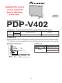
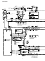
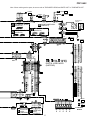
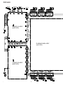
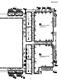
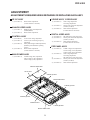
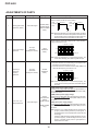
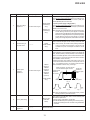
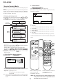
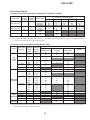
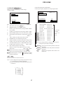
Plasma Field Service Guide
PDP-V401, PDP-V402
& PDP-501MX
Technical Training Department
1925 E. Dominguez Street
Long Beach, CA 90810
Contents
Topic
Page
PDP-V401/402 section
Service manual selection
4
Overall block diagram
5~8
Adjustments
9~12
Troubleshooting
13~14
Service Information
15~16
Tips
17~18
PDP-501MX Section
Overall block diagram
19
Power Down diagnosis
20~21
Adjustments
22~23
Factory service mode
24~28
Tips
29~30
Selecting The correct
service manual for
Models PDP-V402
& PDP-V401
ORDER NO.
ARP3081
PLASMA DISPLAY
PDP-V402
THIS MANUAL IS APPLICABLE TO THE FOLLOWING MODEL(S) AND TYPE(S).
Type
Model
Power Requirement
Remarks
PDP-V402
LUBW/CA/1
AC120V
Confirm it
In PDP-V402, there are two different models (original model and value analysis model).
Confirm the mark and serial No. of the product rear side, and use each service manual.
PRODUCT REAR SIDE
SERIAL NO.
Serial No.
Serial No.
1∗
(
∗∗∗∗
Service Manual
1∗∗∗∗∗
)
ARP3081 [This manual]
ARP3034
OTHER
Discrimination Seal
(SILVER)
ARP2981 (PDP-V401)
4
T
PDP-V402
AC INLET
AKP1211
S1: POWER SW
BSM1010
ADX2584
ADX2586
LIVE
E
E
AC100–120V
50/60 Hz
G
CN5005
Y3
NEUTRAL
CN4001
X10
CN4004
X2
ADX2607
ADX2607
ADX2585
CONTROL (A) ASSY
U OTL
(AWZ6177)
N
CONTROL (A) ASSY
R
K RCC
(AWZ6174)
CN4003
X1
ADX2607
E
F
E
CN4003
X1
CN4005
X3
SUB POWER ASSY
(AWZ6173)
A
C C 1/4- C 4/4
ANALOG VIDEO ASSY
(AWQ1056)
B
CN7354
CN3201
(AWZ6526)
CN7358
CN7355
CN7251
CN7001
RECEIVER
J IR
ASSY
CN3204
CN7850
CN3202
B B 1/6- B 6/6
CONTROL ASSY
(AWZ6545)
RELAY ASSY
K FAN
(AWZ6535)
Y/C ASSY
Q 3D
(AWQ1055)
FAN MOTOR ×5
AXM1039
A
CN3203
C
A A 1/2- A 2/2
ADX2650
22
CN7002
5
CN7000
CN7351
J81
ADX2614
KM250MA8R
CN7650
INPUT CONTROL ASSY
(AWZ6554)
PDP-V402
Note : When ordering service parts, be sure to refer to "EXPLODED VIEWS and PARTS LIST" or "PCB PARTS LIST".
ADX2607
G
CN5004
Y2
ADX2607
G
CN5001
Y16
ADX2361
G CN5003 Y1
H CN5003
ADX2607
B
Y1
FAN MOTOR ×2
AXM1038
CONTROL (B) ASSY
V OTL
(AWZ6178)
S
POWER ASSY
M MAIN
(AWR1077)
T
RCC CONTROL (B) ASSY
(AWZ6175)
RCC CONTROL (C) ASSY
(AWZ6176)
ADX2609
C
E
CN4008
X4
H CN5008
Y5
ADX2630
ADX2646
ADX2652
ADX2651
CN7250
ADX2644
D D 1/10- D 10/10
D.RESET
ADX2341
VGA60_75
ADX2645
CN7501
CN7350
CN7352
DIGITAL VIDEO ASSY
(AWP1069)
CN7003
ADX2608
ADX2649
G CN5007
Y4
and
J7800
H CN5007
Y4
CN7750
L
B8B-PH-SM3
SYNC DET
ASSY
(AWZ6548)
CN7800
I
FRONT KEY
ASSY
(AWZ6525)
6
ADX2639
ADX2632 ADX2633 ADX2633
ADX2634
ADX2635
ADX2636 ADX2638 ADX2638
ADX2637
To ADDRESS
MODULE
23
PDP-V402
N CN1602
SP2
M
CN3203
P6
M
CN3404
P4
D CN6701
E11
M CN3305
P3
D CN6702
E12
D CN6703
E13
D CN6551
E6
E
X DRIVE (A) ASSY
(AWP1078)
PLASMA PANEL ASSY
(AAV1235)
F
X DRIVE (B) ASSY
(AWP1079)
M
CN3305
P3
D CN6706
E16
24
7
D CN6707
E17
D CN6708
E18
PDP-V402
D CN6704
E14
D
CN3304
N CN1602
M CN3405
M P2
SP2
P5
CN6705
E15
M
CN3204
P7
SCAN MODULE (B)
(AXF1105)
D
CN6553
P
E8
G
MODULE (A)
O SCAN
(AXF1104)
P
SCAN MODULE (B)
(AXF1105)
Y DRIVE (A) ASSY
(AWZ6533)
H
MODULE (A)
O SCAN
(AXF1104)
Y DRIVE (B) ASSY
(AWP1077)
D CN6709
E19
D CN6553
E8
M
P2
CN3304
D CN6552
E7
D CN6710
E20
8
25
PDP-V402
ADJUSTMENT
ADJUSTMENTS REQUIRED WHEN REPAIRING OR REPLACING EACH ASSY
3D Y/C ASSY
1) (Procedure 9)
X DRIVE ASSY, Y DRIVE ASSY
White balance adjustment
(if white balance is deviated)
1) (Procedure 5)
2) (Procedure 7)
ANALOG VIDEO ASSY
1) (Procedure 1)
2) (Procedure 9)
3) (Procedure 9)
Blanking pulse width adjustment
(VBLK, HBLK)
White balance adjustment
DIGITAL VIDEO ASSY
1) (Procedure 6)
2) (Procedure 7)
CONTROL ASSY
1) (Procedure2)
2) (Procedure 3)
3) (Procedure 8)
4) (Procedure 9)
VCO control voltage adjustment
Vertical sync freerunning frequency
adjustment
Factory data setting (At ASSY replacement)
(Read the preset data before replacing
ASSY)
White balance adjustment
(if white balance is deviated)
3) (Procedure 9)
DIP SW setting of the pulse value
Sustain pulse waveform adjustment
(X PSUS, Y PSUS)
White balance adjustment
(if white balance is deviated)
PDP PANEL ASSY
1) (Procedure 4)
2) (Procedure 5)
MAIN POWER ASSY
1) (Procedure 4)
VRN voltage adjustment
VH voltage adjustment
Sustain pulse waveform adjustment
(X PSUS, Y PSUS)
White balance adjustment
(if white balance is deviated)
VADR voltage (60V) adjustment
VSUS voltage (170V) adjustment
VOFS voltage (140V) adjustment
3)
4) (Procedure 7)
5) (Procedure 9)
VADR voltage (60V) adjustment
VSUS voltage (170V) adjustment
VOFS voltage (140V) adjustment
VRN voltage adjustment
VH voltage adjustment
DIP SW setting of the pulse value
Sustain pulse waveform adjustment
(X PSUS, Y PSUS)
White balance adjustment
ANALOG VIDEO ASSY
3D Y/C ASSY
X DRIVE (A) ASSY
MAIN POWER ASSY
Y DRIVE (A) ASSY
X DRIVE (B) ASSY
CONTROL ASSY
Y DRIVE (B) ASSY
DIGITAL VIDEO ASSY
9
145
PDP-V402
ADJUSTMENTS OF PARTS
Procedure
Adjustment
Input Signal
Adjusting Point
Adjusting Method
Observe Pin 7 (CBLK) of IC2801, adjust ∆tV shown in Fig. 1 to
150mS ± 20mS, and ∆tH to 1.7mS ± 200nS.
1
Blanking pulse width
adjustment (CBLK)
100% white signal
VR2802 (VBLK)
VR2803 (HBLK)
(ANALOG VIDEO
ASSY)
C BLK
V blanking
period
tV
150µs±20µs
C BLK
H blanking
period
tH
1.7µs±200µs
Fig. 1
Note: When this adjustment is not performed properly, the black
level correction circuit does not operate. The 100% white
signal waveform does not fall towards the black side, and
emission points become inconsistent on the screen.
Adjust TP 7651 so that the DC voltage of point A of the waveform
in Fig. 2 becomes 5V ± 0.1V.
H : 20µs/div V : 2V/div
2
VCO control voltage
adjustment
No-input
(NO SYNC
displayed on screen)
L7650
(CONTROL
ASSY)
5V
A
GND
Fig. 2
Note: When this adjustment is not performed properly, the
screen flows slantingly when NTSC signals are input.
3
Vertical sync
freerunning
frequency
adjustment
No-input
(NO SYNC
displayed on screen)
1. Connect TP K7503 to TP K7502 (GND).
2. Check the waveform of TP 7655 in Fig. 3, and adjust so that
the frequency becomes 43.0Hz ± 0.5 Hz.
3. Then disconnect the TP K7503 and TP K7502 (GND), and
check that the frequency is 52.5 Hz ± 3 Hz.
VR7650
(CONTROL
ASSY)
H : 2ms/div V : 2V/div
GND
Fig. 3
Note: When this adjustment is not performed properly, the
screen moves or flows up and down when NTSC signals
are input.
VSUS (sustain power supply voltage)
Check the drive voltage label value (Note 4), adjust VR3301 so
that value between TP3301 (VSUS) and TP3302 (SUS. GND)
becomes this value.
4
VADR, VSUS, VOFS
voltage adjustment
100% white signal
VR3301
(VSUS)VR3401
(VADR)
VR3601 (VOFS)
(MAIN POWER
Assy)
VADR (address power supply voltage)
Check the drive voltage label value, adjust VR3401 so that value
between TP3401 (VADR) and TP3402 (ADR. GND) becomes
this value.
VOFS (offset power supply voltage)
Check the drive voltage label value, adjust VR3601 so that value
between TP3601 (VOFS) and TP3602 (OFS. GND) becomes
this value.
Note: When the V sus voltage adjustments are not performed
properly, dot-like blinking luminance points appear. If
deviated greatly from the right adjustment, PDP will stop
discharging.
When the VADR and VOFS voltage adjustments are not
performed properly, dot-like blinking luminance points
appear. If deviated greatly from the right adjustment,
these will become white.
146
10
PDP-V402
Procedure
Adjustment
Input Signal
Adjusting Point
Adjusting Method
VRN (minus reset power supply voltage)
Check the drive voltage label value at the top inside the unit,
adjust VR4002 so that value between TP4021 (VRN) and
TP4022 (RNGND) becomes this value.
5
VRN, VH voltage
adjustment
All white 100% signal
VR4002 (VRN)
(X DRIVE (A)
Assy)
VR5002 (VH)
(Y DRIVE (A)
Assy)
VH (scan IC power supply voltage) (Note 1)
Check the drive voltage label value at the top inside the unit,
adjust VR5002 so that value between TP5035 (VHY) and TP5034
(GNDH) becomes this value.
Note: When the VRN voltage adjustment is not performed properly,
dot-like blinking luminance points appear. If deviated
greatly from the right adjustment, PDP will stop discharging.
When the VH voltage adjustment is not performed properly,
dot-like blinking luminance points appear. If deviated
greatly from the right adjustment, these will become white.
Check the pulse value when replacing the DIGITAL VIDEO
ASSY and set the data again for the new Assy with the DIP SW.
6
7
DIP SW setting of
the pulse value
Sustain pulse
waveform
adjustment
––––––
All white 100% signal
S6603
(DIGITAL VIDEO
Assy)
VR6551
(XSUS-U)
VR6552
(YSUS-U)
VR6553
(XSUS-D)
VR6554
(YSUS-D)
(DIGITAL VIDEO
Assy)
Note: If set incorrectly, the number of drive pulses generated will
change, and affect the brightness of the screen. PD
operates if the power consumption exceeds the normal
level.
Check the waveforme shown in Fig.4 at TP4027 (XPSUS),
TP4012 (XPSUS) on the X DRIVE (A) ASSY and X DRIVE (B)
ASSY, TP5004 (YPSUS), TP5002 (YPSUS) on the Y DRIVE (A)
ASSY and Y DRIVE (B) ASSY, then look at the waveform of the
scanned portion, and find the sub field with sustain emission
(refer to Note 2: Sustain emission.)
Enlarge the waveform of the sustain pulse portion shown in Fig.
4 in the sub field with sustain emission, and adjust as shown in
Fig. 5. If not adjusted properly, the slanting portion and base
portion will distort as shown in Fig. 6 and Fig. 7.
Enlarge this portion, and check that this
is the sub field with sustain emission
Typical sub field
adjustment
for Y P.SUS
Reset portion
Scanned portion
Enlarge this
portion and
adjust the pulse
width
Sustain pulse portion
Fig. 4
Fig. 5
Fig. 6
Fig. 7
Note: When the adjustment is not performed properly, dot-like
blinking luminance points will increase.
8
Factory data setting
––––––
9
White balance
adjustment
––––––
Memory data
(CONTROL
ASSY)
When replacing the CONTROL ASSY, read the following data
before ASSY replacement.
1) picture quality, white balance, phase data
2) HOUR METER data (Panel operating time from shipment)
Set the above data again for the new ASSY using the RS232C
command.
Adjust based on the "6.3 WHITE BALANCE ADJUSTMENT". After adjusting,
memorize the setting.
11
147
PDP-V402
Note 1: Take note that GND H differs from the GND potential in
unit.
Note 2: Sustain emission
The sustain waveform must be adjusted using the sub field
with sustain emission. As the scanned portion becomes the
waveform shown in Fig. 8 in the sub field with sustain
emission when 100% white signal is input, find and adjust
this portion. Find it by differentiating it from the scanned
portion of sub fields without sustain emission which has a
distorted waveform as shown in Fig. 9.
Note here
Notes:
÷ The ANALOG VIDEO ASSY (Procedure 1), and CONTROL
ASSY (Procedure 2) (Procedure 3) adjustments need not be
performed again in this unit if these ASSYs have been replaced.
÷ Other adjusting points which need not be adjusted again in this
unit when other ASSYs are replaced are as follows.
MAIN POWER ASSY
VR3501 (STB+5V)
VR3201 (Vcc+5V)
VR3101 (+B 215V)
VR3801 (VSUS UVP)
If distorted here, it means that
the address is selected and
there is no sustain emission.
SUB POWER ASSY
VR1601 (VCSP 40V)
÷ If adjusted VRs of the above MAIN POWER ASSY and SUB
POWER ASSY are rotated accidentally, adjust to the following
values.
Fig. 8
Fig. 9
MAIN POWER ASSY
VR3501 (STB+5V): Adjust the DC voltage value between
TP3501 (STB+5V) and TP3503 (STB.
GND) to +5V±0.1V.
VR3201 (Vcc+5V): Adjust the DC voltage value between
TP3201 (Vcc+5V) and TP3202 (D.
GND) to +5.05V±0.1V.
VR3101 (+B 215V): Adjust the DC voltage value between
TP3101 (+B) and TP3102 (P.GND) to
+215V±0.5V.
VR3801 (Vsus UVP): Adjust the DC voltage value between
the R3860 lead (Pin 6 of IC3805) and
R3863 lead (+ lead of C3814) to
0±10mV.
Note 3: Screen when RAMP signal is input
Note 4: Position where drive voltage label is pasted
SUB POWER ASSY
VR1601 (VCSP 40V): Check the drive voltage label value,
and adjust the DC voltage value between
TP1603 (VCSP) and TP1604 (CSP.
GND) becomes this value.
Drive Voltage Label
Note: Take note that the CSP.GND or GND_H differs from the
GND potential of this unit.
Never short between CSP. GND and other GND or
GND_H and other GND.
12
148
PDP-V402
TROUBLESHOOTING
1. MAIN POWER ASSY
Check the power supply voltages.
Measurement Points
VADR (60V) (TP3401) –– ADR. GND (TP3402)
If normal, LED (D3405) lights.
VSUS (170V) (TP3301) –– SUS. GND (TP3302)
If normal, LED (D3305) lights. (which displays the timing of VCC and VSUS)
POWER ON: lights in red (VCC ON) = lights in yellow (VSUS ON) at 1–2sec
POWER OFF: lights in yellow = lights in red at 1–2sec = LED OFF
(VSUS OFF earlier than VCC OFF)
abnormal POWER OFF: lights in yellow = lights in green = LED OFF
(VCC OFF earlier than VSUS OFF)
VOFS (140V) (TP3601) –– OFS.GND (TP3602)
+B (215V) (TP3101) –– P. GND (TP3102)
VCP (12V) (TP3203) –– CP. GND (TP3204)
+13.5V (TP3205) –– A. GND (TP3206)
VCC (5V) (TP3201) –– D. GND (TP3202)
If normal, LED (D3205) lights.
2. SUB POWER ASSY
Check the power supply voltages.
VCSP (40V) ..... TP1603 CSP. GND ........... TP1604
+12V – YVSUS/2
+12V – XVSUS/2
+12.5V – GND
+12.5V – GND
+12.5V – GND
SP2
SP2
SP3
SP5
SP6
=
=
=
=
=
[Precautions for servicing]
1. As the P.D. circuit starts operating when the rear cover is
removed and the CN5801 connector of the FAN RELAY
ASSY is disconnected, short between TP3802 and TP3803.
2. For normal signals, set the rear selection SW S1201 (INPUT
CONTROL ASSY) to OFF. When G on sync signals are
output by Mac, set the switch to ON to prevent overlapping
of the sync. signal.
Y DRIVE (A) ASSY
X DRIVE (A) ASSY
CONTROL ASSY
ANALOG VIDEO ASSY
INPUT CONTROL ASSY
Note: Take note that the CSP. GND differs from the GND
potential of the unit.
TOP
TP3301
(VSUS)
TP3302
(SUS. GND)
TP3205 TP3202
(+13.5V) (D. GND)
TP3201
(VCC+5V)
TP1603
(+40V)
FAN P. D.
TP3803 TP3802
TP3602
(OFS. GND)
D3205
TP3401
(VADR)
D3305
D3405
TP3204
(CP. GND)
TP3203
(VCP)
SP2
TP3601
(VOFS)
TP1604
(CSP. GND)
TP3206
(A. GND)
TP3402
(ADR. GND)
SP3
TP3101
(+B)
SP5
SP6
TP3102
(P. GND)
SUB POWER ASSY
MAIN POWER ASSY
154
13
PDP-V402
GENERAL INFORMATION
DIAGNOSIS
BURN-IN PROBLEM
Definition of burn-in
7 Panel Burn-In Easing Method
One dot consists of red (R), green (G), and blue (B) phosphors on
plasma display as on CRT. The luminance of each phosphor
deteriorates depending on the cumulative light emission time. The
unbalance of deterioration among the phosphors causes burn-in.
PDP-V402 supports full-frame output in integrator mode.
When an image is burnt on the panel, full-frame output for
considerably long time may ease burn-in.
Full-frame Output Procedure
7 Tendency and Comparison of Burn-In
Tendency of burn-in
On our plasma display, the blue phosphor deteriorates comparatively
earlier than the other two types of phosphors. A burnt area tends to
be yellow.
1. Press the MENU button then the STANDBY/ON button to start
up the device in integrator mode.
2. Select "ADDITIONAL SETUP" using the ± or ≠ key.
P I CTURE PARAMETER
CONTRAST
BR I GHT.
COLOR
TINT
SHARPNESS
POSITION
I N I T.
WHITE BALANCE
ADDITIONAL SET UP
TOTAL INITIALIZE
Comparison with PTV
The tendency of burn-in can be compared between PDP-V402 and
PTV as follows:
¶ A burnt area tends to be yellow in PDP-V402 and PTV.
¶ PDP-V402 shows a lower level of burn-in (inconspicuous) than
PTV at high-intensity display.
¶ At low-level display, however, burn-in is slightly more
conspicuous on PDP-V402 than on PTV.
¶ Despite the differences of tendency, the level of burn-in is about
equal between PDP-V402 and PTV.
7 Prevention or Easing of Burn-In
1. For static display, it is recommended to give priority to red and
green. Avoid static display that partially contains blue peaks.
2. Avoid keeping static display for a long time. Switch static and
dynamic displays as frequently as possible.
3. After static display, use dynamic display three to five times
longer than the static image display.
4. When using static display, vary the pattern to avoid burn-in.
5. For static display, use a screen saver not to keep the same pattern
for a long.
6. When using static display for a long time, set the white balance
as close to yellow as possible (minimize the blue level) in
integrator mode to make burn-in inconspicuous.
128
128
128
128
128
(The above menu is when NTSC is
input to the VIDEO function.)
3. Select "FULL MASK" using the ± or ≠ key and press the SET
key.
P I CTURE PARAMETER
WHITE BALANCE
ADDITIONAL SET UP
COLOR MODE
1
BAUD RATE
4800BPS
AUTO RGB2
OFF
NTSC MASK
BLACK
FULL MASK
OSD
ON
HOUR METER
12345
TOTAL INITIALIZE
4. Select "WHITE" using the ± or ≠ key and press the SET key.
Then the display immediately changes to the full-color mask
screen.
Afterimage
FULL MASK
EXIT
RED
GREEN
BLUE
YELLOW
MAGENTA
CYAN
WHITE
PDP is also subject to the problem of afterimage whose symptoms
are close to those of burn-in. Afterimage is a phenomenon of a
residual static pattern that occurs if the display changes from a longtime static image of a high intensity level to a low-intensity image.
Displaying a dynamic image for some time clears this phenomenon.
Note: OSD display is disabled during full-frame output. Turn the
power off using the STANDBY/ON key or press the SET
key to clear the screen.
14
152
`
SERVICE INFORMATION
Date:
MODEL No.
PDP-V401/LU/CA
PDP-V401E/WYVLD
*
Jan 25, 2001
SER.No.
ALL
ALL
No.:
SI-D01019-G
S/M No.
( 1/1 )
PG
SYMPTOM
#
*
DETAIL
A picture turns yellow / A cell defect appears at a part of a panel after 20,000 hours used.
CAUSE
*
A radiative characteristic of a cell is reduced by Long Term Panel Drive.
This happens only on a panel of the first generation.
SERVICE
REMEDY
*
*
Adjust Vofs from 140V to 150V.
Adjust the voltage of VR3601 between TP3601 and TP3602 in Main Power Assy;
AWR1077.
FACTORY
COUNTER
-MEASURE
*
Only Service Remedy
Ref
*
#
CURRENT
SYMBOL/DESCRIPTION
PIONEER
SERVICE NETWORK
M.EGASHIRA ,MANAGER
BS Service
BS Service
Administration Group
Division
PARTS
PART NUMBER
CO
DE
NEW
PART NUMBER
PARTS
SYMBOL/DESCRIPTION
CORPORATION
NOTE:PARTS CODE
1:Changeable from old to new.
2:Not Interchangeable an all.
3:Interchangeable in both ways
5:Do not use old parts
15
Memo:
MTV01-062
Classify:
NM-70
`
SERVICE INFORMATION
Date:
MODEL No.
PDP-V401/LU/CA
PDP-V401E/WYVLD
PDP-V402/LUBW/CA
PDP-V402E/WYVLDK
*
A
A
A
A
Dec.16,1999
No.:
SER.No.
301701-
SI-B54045
S/M No.
( 1/1 )
PG
SYMPTOM
#
1
DETAIL
A half or quarter of picture becomes white
CAUSE
1
The scan module is not drived normally by change of the specification of photocaplor
SERVICE
REMEDY
1
Please replace all of drive boards.
X drive A assy - AWP1057 Y drive A assy - AWZ6261
X drive B assy - AWP1058 Y drive B assy - AWP1060
FACTORY
COUNTER
-MEASURE
1
The current for drive of photocaplor is increased by changing the constants in X driveA,B
and Y drive A,B.
Note
This service remedy is decided replace the board because of it needs to change many constants and it is
difficult to perform the factory countermeasure at site.
The spare parts number is not changed.
The stock parts in Tokyo has been modified.
Ref
*
#
CURRENT
SYMBOL/DESCRIPTION
PIONEER
M.EGASHIRA
BS
Service
Service
ELECTRONIC
,MANAGER
Engineering Section
Division
PARTS
PART NUMBER
CO
DE
NEW
PART NUMBER
PARTS
SYMBOL/DESCRIPTION
CORPORATION
NOTE:PARTS CODE
1:Changeable from old to new.
2:Not Interchangeable an all.
3:Interchangeable in both ways
5:Do not use old parts
16
Memo:
Classify:
MCA54-045
AA-D1586B
AA-D1729
PIONEER ELECTRONICS SERVICE
July 27, 2005
Enter
Model Number
Go
Service Bulletins
Service Manuals
Tech Tips
Search Results for pdpv4
The link below shows all information available for that model number you selected. Navigating through these links will only display
information related to that specific model number. To retrieve information on another model, type the number on the field at the top
right corner of your screen or click home to start over. You can also navigate throught the top menu and start you search over.
Back to Search
Symptom: Unit displays video for only 1 sec, then goes dark with no on screen display or video.
Cure: Replace AWP1058 and AWZ6173
Models Covered: PDPV402
Tip Date: February 12 2001
The Tech Name: Jeff Andrews
Symptom: Picture is all white and shuts down. Standby light seems normal.
Cure: VH is low. Scan module is loading. Disconnect and check for short to isolate.
Models Covered: PDPV401, PDPV402, PDPV402/1
Tip Date: January 31 2001
The Tech Name: Bob Shoemaker
Symptom: A bright white horizontal stripe appears across the screen. The width of the stripe is 1/4 of the screen height.
Cure: If stripe is in the upper half of the screen, swap the cables in connectors Y11 and Y13 of the Y- Drive A module. If
the problem is in the lower half of the screen, swap the same connectors on Y-Drive B. If after swapping the cables, the
stripe moves to the new screen position, replace the Ydrive. If the stripe stays in the same position, replace the
corresponding scan module. Don't forget to put the cables back in the original positions.
Models Covered: PDPV401, PDPV402
Tip Date: January 24 2001
The Tech Name: Jeff Andrews
Symptom: Dark pix (no luminance) on video or Y/C.
Cure: Solder bridge on R2851 Analog Video.
Models Covered: PDPV401, PDPV402
Tip Date: July 25 2000
The Tech Name: Bob Shoemaker
Symptom: Makes "chirping" sound every second. Shuts down after 10 seconds. Video is dark with lots of snow.
Cure: Found VCSP on sub -power board reading 3V. Should be 42V. Replaced sub-power board.
Models Covered: PDPV401, PDPV402
Tip Date: July 17 2000
The Tech Name: Bernie Shelton
Symptom: "Out of Range" displayed while in RGB mode.
Cure: Limit of video resolution is 640 X 480. Reset computer to lower resolution output.
Models Covered: PDPV400, PDPV401, PDPV402
Tip Date: July 12 2000
The Tech Name: Jeff Andrews
17
Symptom: Set goes in to "power Down" mode within 1 or 2 seconds after turning on.
Cure: Unplug connector P6 from the power supply assy and power up again. If the unit stays on longer, quickly turn off
the unit to prevent further damage. Replace X Drive A and X Drive B. If there is no change after removing P6, replace
the connector and remove P7. It the unit stays on longer, quickly turn it off. The problem is on the "A" side. Further
troubleshooting will be needed to determine where the problem is (Y Drive A, Y drive B, or scan modules). DO NOT USE
THIS METHOD IF THE UNIT STAYS ON LONGER THAN 2 SECONDS TO BEGIN WITH.
Models Covered: PDPV401, PDPV402
Tip Date: July 10 2000
The Tech Name: Jeff Andrews
Symptom: Remote control commands will not pass through the PDPV402 to the PDA4003 down-converter.
Cure: You must use a VGA cable between the plasma and the down -converter that has all 15 pins wired.
Models Covered: PDA4003, PDPV402
Tip Date: February 01 2000
The Tech Name: Bernie Shelton
Symptom: When a XDRIVE A or XDRIVE B is found to be bad.
Cure: Replace both A and B together.
Models Covered: PDPV400, PDPV401
Tip Date: October 26 1999
The Tech Name: Dennis Walden
Symptom: Intermittent no video after turning set off & on.
Cure: The plasma set should be turned on BEFORE the video source.
Models Covered: PDPV400, PDPV401, PDPV402
Tip Date: February 08 1999
The Tech Name: Bernie Shelton
Back to Search
You use this information AT YOUR OWN RISK and are utterly responsible for you own actions and this information is
provided AS-IS! By viewing, printing, or downloading this information, you agree to hold Pioneer Electronics Service,
Inc. and it's employees harmless and without liability and without exception.
© 2001 Pioneer North America, Inc, All rights reserved.
18
86
Pump up
interchangable
AWZ6258
PUMP UP
L ASSY
AB
AD
AF
ADDRESS
MODULE
ADDRESS
MODULE
AWZ6256
PUMP UP
H ASSY
ADDRESS
MODULE
AWZ6252
PUMP UP
D ASSY
E
D
IC2610
PULSE MODULE
IC
PULSE GEN
J
IC1551
SEQUENCE
CONTROL IC
AH
IC1601
PANEL U-COM
DRIVE FAM X5
I
AWZ6225
INDICATOR
ASSY
IC2610
PULSE MODULE
IC
PULSE GEN
AWZ6315
SIDE SW
ASSY
G
AWZ6321 Y DRIVE B ASSY
PANEL DISCHARGE
RESET PULSE GEN
IC3109
DRIVE
PROTECTION
AWZ6324
DC FAN
B ASSY
AWZ6325
DC FAN
C ASSY
AWZ6326
DC FAN
D ASSY
AJ
AK
AL
AWZ6323
DC FAN
A ASSY
H
IC6471
AUTO ZOOM DETECT IC
IC6431
AD CONVERTER
AWZ6322 Y DRIVE B ASSY
PANEL DISCHARGE
RESET PULSE GEN
IC3109
DRIVE PRO
TECTION
C
AWZ6305 VIDEO ASSY
SIGNAL SELECT • NTSC SIGNAL PROCESS
IC4501–4505
IC4507,4103
IC4110,4111
INPUT
SELECT
IC7709,7710
7711
SCAN IC
T
AWZ6227
SCAN B ASSY
IC5101
IC6003
IC5802
INPUT
SELECT
COLOR DEM
SYNC SEP
IC6002
SHARPNESS
&
DETAILCONTROL
U
IC6001
BLACK LEVEL
EXPAND
&
RGB MATRIX
Scan PCB
interchangable
AWZ6228
SCAN C ASSY
IC7809,7810
7811
SCAN IC
V
IC3106
PULSE MODULE
IC
PULSE GEN
AWV1687 RGB ASSY
VIDEO SIGNAL
PROCESS
IC5301,5307,5310
SYNC SEP
IC9001
IC8709,8710
8711
SCAN IC
IC3101
PULSE MODULE
IC
PULSE GEN
ADDRESS BUFFER
A
AWZ6222
PROGRESSIVE
BLOCK
AWZ6257
PUMP UP
K ASSY
AWZ6226
SCAN A ASSY
AI
AG
IC2611
PULSE MODULE
IC
PULSE GEN
S
IC3106
PULSE MODULE
IC
PULSE GEN
STAND-BY POWER GEN
AWZ6224
IR RECEIVE
ASSY
IC2612
DRIVE PRO
TECTION
ADDRESS
MODULE
MAIN POWER GEN
IC6441
PLL IC
IC3703
U-COM
AE
AWZ6255
PUMP UP
G ASSY
IC3101
PULSE MODULE
IC
PULSE GEN
IC1301
IC1351
PICTUER
GRADATION IC1401,1451,1501
CONVERT IC PROCESS MEMORY CONTROL
AWV1689 U-COM ASSY
VARIOUS CONTROL
SIGNAL DETECT
IC3704
EEPROM
AC
ADDRESS
MODULE
AWZ6214 CABLE A ASSY
ADDRESS DATA BUFFER
IC1701,1702,1751,1752,1801,1802
SGRAM
IC1131,1151,1171
AD CONVERTER
POWER SW
AWZ6243 X DRIVE B ASSY
PANEL DISCHARGE
PULSE GEN
AWZ6253
PUMP UP
E ASSY
ADDRESS
MODULE
K
POWER FACTOR CONTROL
•
AC RECTIFY
AC POWER CORD
WITH FILTER
F
AWZ6251
PUMP UP
C ASSY
AXY1029 POWER SUPPLY MODULE
VARIOUS POWER SUPPLY
AC INLET
WITH NOISE
FILTER
IC2611
PULSE MODULE
IC
PULSE GEN
ADDRESS
MODULE
AWZ6215 CABLE B ASSY
ADDRESS DATA BUFFER
AWV1728 DIGITAL VIDEO ASSY
DIGITAL SIGNAL PROCESS
IC1271
IC1242
OSD IC
PLL IC
IC2612
DRIVE
PROTECTION
AA
Y
AWZ6249
PUMP UP
A ASSY
ADDRESS
MODULE
L
AWZ6218 CABLE E ASSY
ADDRESS DATA BUFFER
AWZ6226 CABLE G ASSY
ADDRESS DATA BUFFER
AWZ6242 X DRIVE A ASSY
PANEL DISCHARGE
PULSE GEN
AWZ6250
PUMP UP
B ASSY
ADDRESS
MODULE
O
Q
W
X
Z
AWZ6254
PUMP UP
F ASSY
ADDRESS
MODULE
AWZ6229
SCAN D ASSY
IC7909,7910
7911
SCAN IC
B
AWZ6307
CONTROL
ASSY
AWZ6219 CABLE F ASSY
ADDRESS DATA BUFFER
AWZ6221 CABLE H ASSY
ADDRESS DATA BUFFER
ADDRESS
MODULE
AWZ6332
3D Y/C
SEP ASSY
P
R
AWZ6257
PUMP UP
K ASSY
AE
ADDRESS
MODULE
AWZ6255
PUMP UP
G ASSY
AC
ADDRESS
MODULE
AWZ6253
PUMP UP
E ASSY
AA
N
M
AWZ6217 CABLE D ASSY
ADDRESS DATA BUFFER
ADDRESS
MODULE
AWZ6251
PUMP UP
C ASSY
Y
ADDRESS
MODULE
AWZ6249
PUMP UP
A ASSY
ADDRESS
MODULE
W
AWZ6216 CABLE C ASSY
ADDRESS DATA BUFFER
AWZ6250
PUMP UP
B ASSY
X
PDP-501MX
Overall Block Diagram
19
ADDRESS
MODULE
AWZ6252
PUMP UP
D ASSY
Z
ADDRESS
MODULE
AWZ6254
PUMP UP
F ASSY
AB
ADDRESS
MODULE
AWZ6256
PUMP UP
H ASSY
AD
ADDRESS
MODULE
AWZ6258
PUMP UP
L ASSY
AF
PDP-501MX
Diagnosis of Malfunctions when Power Down (PD) Occurs
ASSY Name
TP NO.
X DRIVE(A)ASSY
When K2609 is H
X DRIVE(B)ASSY
+5V Generation Point
Operating PD
D2604 anode
VCP+12V over-current
•
•
(+) reset circuit over- •
•
current
•
VCP+12V over-current •
•
•
D2703 anode
D3104 anode
D3209 anode
D3320 anode (YA)
D3310 anode (YB)
•
•
(–) reset circuit over- •
•
current
•
•
VH150V over-current •
Faulty Point
Pulse module IC2610, IC2611 peripheral circuit
(+) reset circuit Q2702 peripheral circuit
Q2702G-S signal
XPR-U signal terminal K2611 (5V amplitude)
Pulse module IC3101, IC3106 peripheral circuit
YSUS_MSK FET-Q3206-Q3209 peripheral circuit
CSP_MSK FET-Q3005-Q3006 peripheral circuit
Scan assembly internal bypass FET
Q7701, Q7702 peripheral circuit
YNR_D output FET Q3204 peripheral circuit
YNR_U output FET Q3201 peripheral circuit
Q3204 G-S control signal
Q3201 G-S control signal
YNR_D signal terminal K3117
YNR_U signal terminal K3118
D-D converter circuit mis-operations
• When short-circuited between VH150V and
Y DRIVE(A)ASSY
When K3109 is H
Y DRIVE(B)ASSY
D3322 anode (YA)
D3324 anode (YB)
VH150V over-current
•
•
POWER SUPPLY When the following
are L
MODULE
P12 Pin 5 (PD.XA)
Pin 7 (PD.XB)
P6 Pin 8 (PD.YA)
Pin 0 (PD YB)
PD only at small signal
block
(Large Power line off)
Note)
•
•
PD at the large power
block
VCSP +40V
VSUS +175V
VOFS +150V
VRN –190V
•
GND
• Scan IC fault
• D-D converter fault
When not short-circuited between VH150V and
GND
• VH over-current mode (BYPASS FET is
always ON)
• BYPASS output FET short-circuited
• Digital section BYPASS control signal fault
• Control signal stuck
• VH over-current mode (Scan IC misoperations)
• Scan IC fault
• Scan IC control signal fault
• VSUS 175V line fault
When small signal block power overload
• Fault of small signal block power supply of
assemblies
• Fault of only the POWER SUPPLY MOD.
When not small signal block power overload
• Fault of the POWER SUPPLY MOD. when PD
occurs in the POWER SUPPLY MOD. alone
• Fault of assembly when PD does not occur in
the POWER SUPPLY MODULE alone
When large power block overload
• Fault of power supply of each drive assemblies
• Fault of the POWER SUPPLY MOD.
When not large power block overload
• Fault of the POWER SUPPLY MOD. when PD
occurs in the POWER SUPPLU MOD. alone
• Drive circuit mis-operations when PD occurs
due to drive assembly operations
• Drive control signal fault
• Pulse module IC input signal fault
Between SUS-B 4 and 6 of IC2610 (XA)
Between SUS-U 5 and 6 of IC2611 (XB)
Between SUS-D ! and @ of IC3101-1 (YA)
Between SUS-G * and ( of IC3106 (YA)
• Fault between FET and G of each output
Note) If PD occurs without +5V supplied to the PD terminal of the drive assembly, overload of the power supply or malfunction of the POWER
SUPPLY MOD. may be suspected. Turn OFF the large power ON/OFF switch SW1 of POWER SUPPLY MOD., and short-circuit Pins
1 to 3 of CN3305 of each assembly of Y DRIVE (A)/(B) so that only the small signal block can be checked.
83
20
PDP-501MX
E X DRIVE A/B ASS'Y
Q2702
IC2610
IC2611
D2604
D2703
K2609
K2611
G Y DRIVE A ASS'Y
D3209
Q3201
Q3204
IC3106
IC3101
K3109
D3322
D3320 D3104
CN3305
H
Y DRIVE B ASS'Y
Q3201 Q3204
IC3101
D3209
IC3106
K3109
D3104
D3324
D3310
CN3305
84
21
PDP-501MX
ADJUSTMENT
Note: Position for pasting the drive voltage label
Adjustments of Parts
Drive voltage label ARW1077
Note)
In these adjustments, assembly are indicated by the following
symbols.
A :ANALOG VIDEO ASSEMBLY
B :PROGRESSIVE BLOCK
J :POWER SUPPLY MODULE
G :Y DRIVE (A) ASSEMBLY
H :Y DRIVE (B) ASSEMBLY
Procedure
1
Adjusting Item
TINT
Input Signal
Adjusting Point
Adjusting Method
Chroma modulation
ramp signal
VR9002
( A )
Adjust so that the output of Pin 2 (R-Y signal) of CN9505 becomes
minimum.
Adjust so that the amplitudes of a and b become equal at the output
of Pin 4 of CN9505.
2
B-Y demodulation
EIA colour bar
angle
VR9005
( A )
a
b
3
Colour (B-Y)
EIA colour bar (Colour
saturation 75% only) VR9003 ( A )
Adjust so that the output of Pin 4 (B-Y signal) of CN9505 becomes
0.525 Vp-p ±10 mV.
4
Colour (R-Y)
EIA colour bar (Colour
saturation 75% only)
VR9004 ( A )
Adjust so that the output of Pin 2 of CN9505 becomes 0.525 Vp-p
±10 mV.
5
Deflection PLL
adjustment
Any standard
signal
L4715 ( B )
Adjust so that the voltage of TP K4701 becomes 2.6 ± 0.1V.
6
Acquisition PLL
adjustment
Any standard
signal
Adjust the timing of the waveforms of Pin 3 (CLP) of CN4703 and TP
K4702 (HRA) so that the rising edge of the HRA pulse are at the
center of the CLP pulse.
L4706 ( B )
CLP
HRA
Center± 0.2µs
7
VCO free-run
NTSC RAMP signal
frequency for 910 (with burst and chroma)
fH clock
VR3350
( AP )
Set the input to "C.VIDEO", observe the voltage of Pin 7 of IC3352
(TP P3350), and adjust so that the voltage becomes 2.5V ± 0.1V using
the digital voltmeter.
8
Y/C mode chroma NTSC RAMP signal
signal output level (S terminal signal with
burst and chroma)
VR3351
( AP )
Set the input to "S.VIDEO", observe the Q3354 emitter using the
oscilloscope, and adjust so that the level of the chroma signal becomes
400 mV ± 20 mV.
9
VH_A, VH_B
voltage
adjustment
100% white signal
VH A (Scan IC power supply voltage A)
Check the drive voltage label value at the upper left side of the unit
inside, and adjust RV3302 so that the voltage between Pin 1 (VH_
A) and Pin 4 (GND H_A) of the check connector CN3303 becomes
VR3302 ( G )
that value.
VR3301 ( H ) VH B (Scan IC power supply voltage B)
Check the drive voltage label value at the upper left side of the unit
inside, and adjust VR3301 so that the voltage between Pin 1 (VH_B)
and Pin 4 (GND H_B) of the check connector CN3304 becomes
that value.
22
38
PDP-501MX
Procedure
10
Adjusting Item
Input Signal
VSUS, VOFS, VADR,
VCSP, VRN voltage 100% white signal
adjustment
Adjusting Point
RV7, RV5,
RV3, RV4,
RV9 ( J )
Adjusting Method
VSUS (Sustain power supply voltage)
Check the drive voltage label value at the upper left side of the
unit inside, and adjust RV7 so that the value between TP CH24
(175V) and TP-CH25 (175 GND) becomes that value.
VOFS (Offset power supply voltage)
Check the drive voltage label value at the upper left side of the
unit inside, and adjust RV5 so that the value between Pin 1 of
CN3106 (150V) and Pin 4 of CN3105 (SUS, GND) inside the Y
drive assembly becomes that value.
VADR (Address power supply voltage)
Check the drive voltage label value at the upper left side of the
unit inside, and adjust RV3 so that the value between TP CH22
(30V) and TP-CH23 (30V GND) becomes that value.
VCSP (CSP power supply voltage)
Check the drive voltage label value at the upper left side of the unit
inside, and adjust RV4 so that the potential between Pin 4 (CSP)
and Pin 1 (150V) of CN3106 of the Y drive assembly becomes
that value.
VRN (Minus reset power supply voltage)
Check the drive voltage label value at the upper left side of the
unit inside, and adjust RV9 so that the value between TP CH26
(190V) and TP CH25 (175 GND) becomes that value.
If the U-COM assembly has been replaced, mount the former EEPROM (IC3704 24LC64 (I) SN) in the new U-COM assembly.
Note: CSP, GNDH_A, and GNDH_B differ from the GND potential in the unit. The GND potentials are also different each other.
• The adjustment tolerance of the drive voltage label is ± 0.5V.
• The adjustments of the ANALOG VIDEO ASSEMBLY (step 1), (step 2), (step 3), (step 4), (step 5), and (step 6) is not necessary when
replacing this assembly.
• Adjusting points which need not be adjusted again in the unit after replacing other assemblies are as follows.
SW power supply
RV8 (+5V)
RV6 (+3.3V)
RV2 (+12V)
RV1 (+5VSTB)
• If the above adjustment controls are rotated by mistake, adjust to the following values;
RV8 (+5V): Adjust the DC voltage between TP CH16 (5V) and TP CH19 (5V GND) to 5.0V ± 0.1V.
RV6 (+3.3V): Adjust the DC voltage between TP CH17 (3.3V) and TP CH19 (5V GND) to 3.3V ± 0.066V.
RV2 (+12V): Adjust the DC voltage between TP CH18 (12V) and TP CH19 (5V GND) to 12.0V ± 0.24V.
RV1 (+5VSTB): Adjust the DC voltage between TP CH4 (5V) and TP CH19 (5V GND) to 5.0V ± 0.1V.
White Balance Adjustment
Set COLOUR to minimum and the other video settings to the
standard setting in the following measurements.
1. Black level adjustment
1) Input the RAMP signal.
2) Monitor the output TP terminals of the RGB assembly (R:P5802,
G:P5801, B:P5803), and adjust R,G,B LOW LIGHT so that the
black level (0IRE) becomes 2.6V.
2. LOW LIGHT adjustment
Input the RAMP signal, and adjust R, G, B:LOW LIGHT so that
the point which starts to light up becomes gray.
3. HIGH LIGHT adjustment
(Reference)
Adjustment values using the Minolta colour-difference meter
CA-100
80% window step 0dB
[NTSC] [HDTV]
x=300
y=315
Y=58 ± 15cd/m2
20% 4.0cd/m2 (NTSC)
3.0cd/m2 (HDTV)
[RGB]
x=290
y=315
Y=35 ± 10cd/m2 (20% 2.5cd/m2)
Checking picture quality
1) Input the RAMP signal.
2) Monitor the TP terminals of the RGB assembly (R:P5802,
G:P5801, B:P5803), and adjust R,G,B HIGH LIGHT so that the
white level (100IRE) becomes 4.4V.
3) Input the white signal (80IRE).
4) Adjust R,G,B HIGH LIGHT so that the screen becomes reddish
white (T=7200K, dev=0.000uv).
4. Adjusting voltage check
Input the RAMP signal, monitor the TP terminals of the RGB
assembly (R:P5802, G:P5801, B:P5803), and check that the black
level (0IRE) is 2.6V ± 0.1. The white level (100IRE) value is not
specified.
23
1. Face colour check (Colour balance check)
After adjusting the white balance, check the face colour of figures
in LD still pictures.
If the colour is not natural, adjust COLOUR and TINT and
memorize the value.
2. Picture quality check
Set the sharpness to 120 for both NTSC and HDTV, and the detail
setting to 70 for NTSC and 65 for HDTV, and check the picture
quality.
Note: Adjust the white balance and check the picture quality in each
NTSC screen mode (natural wide, zoom, etc.) and HDTV
(MUSE).
39
PDP-501MX
Service Factory Mode
This mode is used for checking the operations and setting the picture
quality.
Perform the operations of the service factory mode using the remote
control unit provided with the PDP-501MX (CU-PDP002:
AXD1437) and the remote control unit provided with the PDP501HD (CU-PDP001: AXD1432).
3. RANGE CHECK
( Front Surround key)
Mode for checking the operations of the circuits.
Each time this key is pressed, the mode changes from center,
maximum, to minimum.
RANGE
1. Entering the factory mode
MODE
EA /
Current main menu
In the standby state, press the remote control keys Menu , Set ,
and Power in this order within 3 seconds. (See figure below ‘.)
Or in the ON state, send the <FAY> command of RS-232C.
In service
factory mode
Service factory Mode
Normal operation
mode
Menu
<FAN>
SERVICE MENU
Display
Mute
RANGE CHECK
Mute
: 128
Range (center, maximum,
and minimum)
CONTRAST
Setting
parameter
(Standby)
Front surround
Mute
Keys
1 COLOUR
Center→Maximum→Minimum (Each time key 1 is pressed)
2 CONTRAST
Center→Maximum→Minimum (Each time key 2 is pressed)
3 SHARP (NESS)
Center→Maximum→Minimum (Each time key 3 is pressed)
4 CLK FRQ.
Center→Maximum→Minimum (Each time key 4 is pressed)
PICTURE
Standard/AV memory
Mute
COLOUR and SHARP cannot be used for RGB (PC/VIDEO (RGB
input)).
INITIALIZE
POWER
Bilingual
STANDBY/ON
• When the service factory mode is set, the video and the screen
will be reset.
• In the service factory mode, the Mute key functions to change
the mode in the following order;
SERVICE MENU→RANGE CHK.→PICTURE→INIT.
The other keys Display , Front Surround , Standard/AV
memory , and Bilingual function to switch the mode directly.
• In the factory mode, press the Menu key to set the normal
operation mode.
INPUT1
INPUT2
INPUT3
INPUT4
VIDEO
S-VIDEO
C.VIDEO
( RCA )
RGB
( BNC )
RGB
( D-sub )
FULL AUTO
ZOOM
SCREEN
SIZE
DISPLAY
MENU
SET
DISPLAY
MENU
MUTE
Front
Surround
Volume +
SET
Standard
/AV memory
Volume –
2. SERVICE MENU ( Display Call key)
Bilingual
Information mode
PD5435A
TV SYSTEM
CONTROL µ-COM'S
Version
PLASMA DISPLAY
REMOTE CONTROL UNIT
MODE
1
2
3
4
Î
EA /
Image signal
discrimination
Screen size
Signal type
5
6
7
8
9
10
11
12
BS 1
BS 3
BS 5
BS 7
BS 9
BS 11
BS 13
BS 15
WIDE PLASMA DISPLAY
REMOTE CONTROL UNIT
• Refer to the table on the next page for details on the video signal
type and screen size.
• Signal state [ / ]:Composite, Y/C
[+]:Component (Colour difference signal)
[None]:RGB
Note: The EA/ in the above example indicates that the signal input
is the NTSC (15.7 kHz/60 Hz) and screen size is NATURAL
WIDE.
40
Remote control unit provided
with the PDP-501MX
(CU-PDP002: AXD1437)
Remote control unit provided with
the PDP-501HD
(CU-PDP001: AXD1432)
<Note> Do not press keys nor make changes in the
factory mode other than the adjustment items
indicated in the service manual.
24
PDP-501MX
List of Input Signals
(1) Table of video input signals (When setting INPUT 1,2/INPUT 3,4:VIDEO)
Input signal
Horizontal
frequency
Fh (kHz)
Vertical
frequency
Fv (Hz)
15.734
60.0
31.5
60.0
45.0
60.0
33.75
60.0
NTSC, SDTV480i
Double-speed
NTSC, SDTV480i
HDTV 720P
HDTV1080i
Screen size...On Screen Display
Signal format
4:3NORMAL
FULL
ZOOM
CINEMA WIDE NATURAL WIDE
E8/
E6/
E7/
S/video
E9/
EA/
....................................................................................................................................
E8+
E6+
E7+
Component
E9+
EA+
....................................................................................................................................
ED
EC
EB
RGB (Note)
EE
EF
F8+
F7+
F6+
Component
F9+
FA+
....................................................................................................................................
F8
F6
F7
RGB
F9
FA
J2+
Component
....................................................................................................................................
J2
RGB
G2+
Component
....................................................................................................................................
G2
RGB
Note: The NTSC-RGB signal can be used only when the key p STD-RGB (standard speed RGB enable setting) of ''5. INITIALIZE MODE"
is set to on. It is not displayed at the factory setting (OFF).
(2) List of PC input signals (When setting INPUT 3, 4:PC)
Model
Input signal
Dot x line
640∗400
640∗480
NEC
PC-9800
series
800∗600
1024∗768
1280∗1024
640∗400
640∗480
800∗600
IBM PC/AT
compatibility
1024∗768
Apple
Macintosh
Exclusive
Videocard
Horizontal
Frequency
Fh (kHz)
(Note)
Vertical
Frequency
Fv (Hz)
(Note)
Screen size .... On Screen Display
ORIGINAL or
ORIGINAL (TYPE)
4:3 NORMAL or
4:3 (TYPE)
FULL or
FULL (TYPE)
ZOOM
B0
B2
N0
N2
N1
70.1
31.5
F0
F2
F1
59.9
31.5
.................................................................................................................................................................
R0
75.0
37.5
I0
I2
I1
60.3
37.9
.................................................................................................................................................................
S0
S2
S1
75.0
46.9
O1
O2
70.1
56.5
.................................................................................................................................................................
U1
U2
75.0
60.0
B1
56.4
24.8
.................................................................................................................................................................
L2
L1
60.0
64.0
L3
N0
N2
N1
70.1
31.5
.................................................................................................................................................................
F0
F2
F1
59.9
31.5
.................................................................................................................................................................
P0
72.8
37.9
.................................................................................................................................................................
R0
75.0
37.5
C0
C2
C1
56.3
35.2
.................................................................................................................................................................
I0
I2
I1
60.3
37.9
.................................................................................................................................................................
Q0
Q2
Q1
72.2
48.1
.................................................................................................................................................................
S0
S2
S1
75.0
46.9
K1
K2
60.0
48.4
.................................................................................................................................................................
O1
O2
70.1
56.5
.................................................................................................................................................................
U1
U2
75.0
60.0
.................................................................................................................................................................
21
22
87.0
35.5
1280∗1024
640∗480
832∗624
1024∗768
1152∗870
64.0
35.0
49.7
60.2
68.7
60.0
66.7
74.6
74.9
75.1
1280∗768
45.1
56.3
M0
T0
U1
V1
L2
M2
T3
U2
V2
D1
D2
L1
M1
M2
L3
Note: The input signal frequency displayed when the remote control key DISPLAY is pressed is the typical values of each signal mode, and
may differ from the actual input signal frequency.
25
41
PDP-501MX
4. PICTURE ( Standard/AV Memory Key)
(2) Parameter adjustment (When REFERENCE is selected)
Mode for selecting the video tables to be adjusted.
(1) Menu in mode
REFERENCE
MODE
EA /
Current selected mode
PICTURE
MODE
EA /
Current main menu
CONTRAST
: 128
Setting parameter
Adjustment value
REFERENCE
Keys
1
2
3
4
5
6
7
8
9
p
q
w
BS5
BS9
BS11
Current video and audio table
Keys
1 REFERENCE
5 COLOUR TEMP1
Colour temperature offset
Not necessary to readjust
6 COLOUR TEMP2
Fix at the factory setting
7 COLOUR TEMP3
8 COLOUR TEMP4
9 GAME
Offset memorized for selection
p LIVING
Not necessary to readjust
q CINEMA
Fix at the factory setting
w SPORTS
Keys 2 to w cannot be used when INPUT SETTING is set to
PC.
3 Set key
Sets the mode and moves to the lower level.
CONTRAST
BRIGHT (NESS)
COLOUR
TINT
SHARP (NESS)
DETAIL
R HIGH
G HIGH
B HIGH
R LOW
G LOW
B LOW
B-Y GAIN
BLK LEV START
BLK LEV GAIN
(000 to 255)
(000 to 255)
(000 to 127)
(000 to 127)
(000 to 255)
(000 to 255)
(000 to 255)
(000 to 255)
(000 to 255)
(000 to 255)
(000 to 255)
(000 to 255)
(000 to 063)
(000 to 015)
(000 to 015)
Commands
<CNT>
<BRT>
<COL>
<TNT>
<SHP>
<DTL>
<RHI>
<GHI>
<BHI>
<RLW>
<GLW>
<BLW>
Not necessary to
readjust
Fix at the factory
setting
Note: Do not change the factory settings for BS1 and BS3 .
If changed, the panel may be damaged.
3 Volume + Increases the value of the parameter selected for
adjustment
<UPn> *
Volume – Decreases the value of the parameter selected for
adjustment
<DWn> *
Set
Memorizes the adjusted value and moves to a
higher level
*
<NOTE>
When messages not indicated in the service manual are
displayed on the screen, turn OFF the power promptly.
And exit the service factory mode.
Changing the data not indicated in the service manual
unintentionally may result in the damage of the unit.
26
42
n: 0~9, F
1→1
2→2
•
•
•
0→10
F→Full
PDP-501MX
(2) Parameter adjustments (SUB VIDEO)
Common picture quality adjustment for all input signal modes.
5. INITIALIZE ( Bilingual key)
Mode for changing and checking the initial settings.
(1) Menu in mode
SUB VIDEO
INITIALIZE
MODE
EA /
MODE
EA /
Current selected mode
Current main menu
SUB VIDEO
SUB CONTRAST
: 127
Setting parameter
Adjustment value
Current selected menu
Keys
Commands
1
SUB VIDEO (Set using the SET key.)
2
MIRROR_MODE (Inverted Picture mode)
OFF/XY cyclic (OFF at the factory setting) <MMN>/<MMZ>
3
FULL MASK
ON/OFF-cyclic (OFF at the factory setting) <FMY>/<FMN>
5
HOUR METER (Displays the current hours meter) <HMD>
6
BAUD RATE (Sets the RS-232C communication speed with
PC)
<BRm> *
1200 to 19200 cyclic (4800) at the factory setting
7
EEPROM INIT. (For manufacturing line only)
8
MASK CONTROL (Automatic mask position change setting)
ON/OFF cyclic (ON at the factory setting) <MCY>/<MCN>
p
STD-RGB (Standard speed (15. 734kHz) RGB enable setting)
ON/OFF (OFF at the factory setting)
<NRY>/<NRN>
q
INTE. MODE (Integrator mode setting)
FREE, ON, LOCK cyclic (FREE at the factory setting)
(Menu OFF)
<IMF>/<IMY>/<IMN>
BS1 FINAL SETUP (factory setting) Set using the Set key
(Recovers the initial setting) Refer to next page. <FST>
BS3 IPQ ADJ (Progressive conversion Not necessary to readjust
Fix at the factory setting
parameter adjustment)
Keys
1
2
3
9
p
q
BS3
BS5
BS7
BS11
BS13
BS15
SUB CONTRAST (000 to 127)
ACL START
(000 to 015)
ACL GAIN
(000 to 015)
ACL SW ACL SW ON/OFF cyclic
VAP GAIN
(000 to 007)
VAP INV
(000 to 031)
R SIDE LEV
(000 to 255)
G SIDE LEV
(000 to 255)
B SIDE LEV
(000 to 255)
R FULL LEV
(000/255)
G FULL LEV
(000/255)
B FULL LEV
(000/255)
Not necessary
to readjust
Fix at the
factory
setting
Note: Do not change the factory settings for keys 6 and 8.
If changed, the panel may be damaged.
3 Volume +
Volume –
Set
Increases the value of the parameter selected for
adjustment
Decreases the value of the parameter selected for
adjustment
Memorizes the adjusted value and moves to a
higher level
Set (1, BS1 )
Sets the mode and moves to the lower level.
Note: 1) Do not change the factory settings for the modes of keys
9 . If changed, the panel may be damaged.
2) Be sure to turn the key 3 FULL MASK off when the power
is turned off.
*
m: 1~5
1→1200bps
2→2400bps
3→4800bps
4→9600bps
5→19200bps
27
43
PDP-501MX
(3) Details of FINAL SETUP
Item
Input function
FULL AUTO ZOOM
Screen size
V.POSITION
KEY LOCK
PICTURE
SCREEN
V MEMORY
(RECALL)
V MEMORY
(MEMORY)
AUTO POWER OFF
3D Y/C MODE
INPUT SETTING
SIGNAL
CLAMP
ABL
MP MODE
PICTURE
WHITE BALANCE
SCREEN
COLOUR MODE
BAUD RATE
HOUR METER
MIRROR MODE
STD-RGB
SIDE MASK
FULL MASK
MASK CONTROL
INTE. MODE
ACL SW
CTI
VNR
ID No.
OSD
note 1
<SM0>: Original
<SM1>: 4:3 Normal
<SM2>: Full
<SM3>: Zoom
<SM4>: Cinema Wide
<SM5>: Natural Wide
44
Commands
Initial Setting
Remarks
<IN1~4>
INPUT1
<AZY> / <AZN>
OFF
Common for all input functions
NATURAL
WIDE
VIDEO
................................................................................................................................... <SM0~5>
PC1 4:3 NORMAL (Including TYPE)
mode D,E,L,V
note 1
...................................................................................................................................
PC2 ORIGINAL (Including TYPE)
mode B,C,F,I,K,M,N,O,P,Q,R,S,T,U,X,Y,Z,2
<UPS>
0
Input functions
<KLY> / <KLN>
UNLOCK
note 2
Center value for all adjustment items
note 3
Center value for all adjustment items
STANDARD
Input functions (VIDEO)
..........................................................................................................................................................
STANDARD
Input functions (VIDEO-RGB)
..........................................................................................................................................................
STANDARD
Input functions (PC-RGB)
GAME
(MEMORY
1)
.............................................................................
LIVING (MEMORY 2)
.............................................................................
VIDEO
CINEMA (MEMORY 3)
.............................................................................
SPORTS (MEMORY 4)
USER A to D (STANDARD for all memory contents)
RGB
..........................................................................................................................................................
USER A to D (STANDARD for all memory contents)
PC
<APY> / <APN>
OFF
Common for all input functions
<YCS / <YCM>
STILL
COMPONENT 2(SMPTE170M)
INPUT2
..........................................................................................................................................................
PDP-501
PC
VIDEO
PDP............................................................................. INPUT3
RGB (Fixed) V501X
COMPONENT 1 MX/KUC
..........................................................................................................................................................
PC
.............................................................................
INPUT4
RGB (Fixed)
MODE1
ON
ON
(Adjustment values for all adjustment items)
(Adjustment values for all adjustment items)
Center value for all adjustment items
1
4800BPS
For each setting-INPUT 3, 4
For each setting-INPUT 3, 4 PC
For each setting-INPUT 3, 4 PC
Memory contents cleared for PC
Memory contents cleared for PC
<CL1> / <CL2>
<ABY> / <ABN>
<MPY> / <MPN>
note 2
note 3
<CM1> / <CM2>
<BR1~5>
<MMN> / <MMZ>
OFF
Common for all input functions
<NRY> / <NRN>
OFF
Common for input functions
<RSL>
R
LEVEL:
56
..........................................................................................................................................................
<GSL>
G
LEVEL:
56
..........................................................................................................................................................
<BSL>
B LEVEL: 112
<FMY> / <FMN>
OFF
<MCY> / <MCN>
ON
FREE (PDP-V501X)
ON
ON
3
LOCK (PDP-501MX/KUC)
<IMF>/<IMY>/<IMN>
<IDS> / <IDC>
<DIY> / <DIN>
ON
note 2
<CNT>: Contrast
<COL>: Color
<TNT>: Tint
<SHP>: Sharp
<BRT>: Bright
<DTL>: Detail
<RHI>: R High
<RLW>: R Low
<GHI>: G High
<GLW>: G Low
<BHI>: B High
<BLW>: B Low
28
note 3
<VPS>: V. Pos 1
<HPS>: H. Pos 1
<CFR>: CLK FRQ
<CPH>: CLK PHS
PIONEER ELECTRONICS SERVICE
August 25, 2005
Enter
Model Number
Go
Service Bulletins
Service Manuals
Tech Tips
Search Results for pdpv501
The link below shows all information available for that model number you selected. Navigating through these links will only display
information related to that specific model number. To retrieve information on another model, type the number on the field at the top
right corner of your screen or click home to start over. You can also navigate throught the top menu and start you search over.
Back to Search
Symptom: Picture tears with 480P component. New!
Cure: Replace RGB, AWV1687.
Models Covered: PDP501MX, PDPV501X
Tip Date: July 27 2005
The Tech Name: Bob Shoemaker
Symptom: Unit turns on, but no pix or OSD. No scan pulses from Dvid.
Cure: Replace RGB, AWV1687. No VD out.
Models Covered: PDP501MX, PDPV501X
Tip Date: January 21 2004
The Tech Name: Bob Shoemaker
Symptom: 1" WIDE LINE IN TOP OR BOTTOM 1/2 THAT CHANGE COLOR, ETC WHEN TOUCHING RIBBONS TO OR
FROM CABLE ASSY.
Cure: CHECK FOR UNLOCKED OR CRACKED CONNECTORS ON UCON OR DVID.
Models Covered: PDP501MX, PDPV501X
Tip Date: December 31 2002
The Tech Name: Bob Shoemaker
Symptom: Intermittant power down. No PD pulse and all supplies OK.
Cure: 27k resistor had cracked solder. Located by RV4 & 5. Probably 150V OVP detector.
Models Covered: PDP501MX, PDPV501X
Tip Date: January 17 2002
The Tech Name: Bob Shoemaker
Symptom: Distorted, out of sync, or no picture with PC connected on input #3 or #4. Other sources on other inputs
were fine. Tried several computers with numerous settings with no result. Replaced the RGB board assy.(AWV1687)
and still had same symptom.
Cure: Replaced the system control board (AWV1689) and restored normal operation.
Models Covered: PDPV501
Tip Date: October 22 2001
The Tech Name: Tony Perkins
Symptom: Top 1/2 of pix is white after replacing YA & scan for PD.
Cure: CN7111 (T15) of Cable B plugged in crooked (no Vadr or 3vcc).
Models Covered: PDP501MX, PDPV501X
Tip Date: December 12 2000
The Tech Name: Bob Shoemaker
29
Symptom: Shuts down after 6 seconds. Gives no display.
Cure: Y Drive B board PD (power down) test point went high just before the unit shut down, but the problem was in one
of the scan boards connected to Y Drive A board. Troubleshoot by unplugging the scan assemblies one at a time. You
must leave power off at least a minute before reconnecting the scan board to allow charge to dissipate.
Models Covered: PDP501MX, PDPV501X
Tip Date: October 10 2000
The Tech Name: Bernie Shelton
Symptom: When replacing the protective panel, page 8, #4,
Cure: you must also replace the "Panel Cushions" and "Shield Gaskets" because the are sticky and can't be removed
from the old protective panel.
Models Covered: PDP501, PDPV501
Tip Date: May 12 2000
The Tech Name: Bernie Shelton
Symptom: Troubleshooting procedure for P.D.
Cure: Check for PD pulse at Power Supply connectors- P4 pin 8 (Temp_PD), P12 pin 5 (X Drv A), P12 pin 7 (X Drv B), P6
pin 8 (Y Drv A), and P6 pin 10 (Y Drv B). (P2 pin 9 is labeled PD AU, but is not connected to anything on the U -CON
Assy.)
Models Covered: PDP501MX, PDPV501X
Tip Date: December 20 1999
The Tech Name: Dennis Walden
Symptom: When replacing the U-Com Assy AWV1689, some original PCB's did not have a connector for E15 (3 wires
from Side Sw Assy). The wires may be soldered to the PCB.
Cure: The new PCB is different. There are 3 solder pads located next to E13 connector labeled Blue Wire, White Wire,
and Red wire.
Models Covered: PDP501MX, PDPV501
Tip Date: December 14 1999
The Tech Name: Dennis Walden
Symptom: Power LED comes on in Green when main pwr is applied, but no video or OSD.
Cure: Listen for noise level of unit to drop after a few seconds. Unit is shutting down. Troubleshooting in s/m is
incorrect. Display LED will not blink. See Diagnosis on page 83 and PD Block on page 85.
Models Covered: PDP501MX, PDPV501X
Tip Date: December 01 1999
The Tech Name: Dennis Walden
Back to Search
You use this information AT YOUR OWN RISK and are utterly responsible for you own actions and this information is
provided AS-IS! By viewing, printing, or downloading this information, you agree to hold Pioneer Electronics Service,
Inc. and it's employees harmless and without liability and without exception.
© 2001 Pioneer North America, Inc, All rights reserved.
30