1
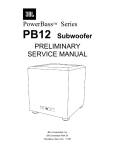
TM PowerBass Series PB12 Subwoofer SERVICE MANUAL JBL Incorporated 250 Crossways Park Dr. Woodbury, New York 11797 REV2 10/2001 PB12 TABLE OF CONTENTS Safety Information ……………………………………………………….3 Basic Specifications ………………………………….………………….4 Detailed Specifications ………………………………………………….5 Controls and their Function …………….……………………………….6 Speaker Connection …………………….……………………………….7 Operation ………………………………….….………………………….10 Troubleshooting………………………………………………………….11 Test Setup and Procedure ……………………………….…………….12 Service Bulletin JBL 2001-03 ………………………………………….13 Service Bulletin JBL 2001-05 ………………………………………….14 Service Bulletin JBL 2001-07 ………………………………………….15 Exploded and Packaging ………………………………...…………….16 Amplifier Exploded View ……………………………………………….17 Amplifier Faceplate …………………………………..…………………18 Integrated Circuit Diagrams…………………………………………….19 Testing Procedure…………………………………….…………………20 Electrical Parts List (PCB version 6.3 – 7.0)………………………….23 Electrical Parts List (PCB version 7.2) …………………………..……28 Printed Circuit Boards (PCB version 6.3 – 7.0)…… ……...…..…….32 Printed Circuit Boards (PCB version 6.4)………..… ……...…..…….35 Printed Circuit Boards (PCB version 7.2)…… ……...……………….36 Schematics Preamp (PCB version 6.3 – 7.0)…………………… ………….39 Power Amp (PCB version 6.0 – 6.3)…………..……………….40 Power Amp (PCB version 7.0)………………………………….41 Preamp (PCB version 7.2)…………………………….. ……….42 Power Amp (PCB version 7.2)………………………………….43 2 PB12 SAFETY INFORMATION 100V 4.7uF 3 PB12 BASIC SPECIFICATIONS PB12 Subwoofer 4 PB12 DETAILED SPECIFICATIONS PB12 Subwoofer 5 PB12 PB12 Subwoofer Controls and their Function 1. Power - These lights will be red when the unit is plugged in and not receiving a signal; when the PB12 receives a signal, the lights will cycle to GREEN. If no signal is received after 10-15 minutes the lights will cycle back to RED (standby) until a signal is present again. 2. Level Control - The subwoofer Level Control, PB12, (located on the rear panel) adjusts the volume of the subwoofer relative to the rest of the system. 3. LFE/Normal Switch - Ordinarily placed in the Normal position - but switch to LFE when playing Dolby DigitaL, DTS or other digital surround modes - see page 9. 4. Phase Switch - Changes the subwoofer’s output to be in phase or 180 degrees out of phase with the program material. Front Panel Rear Panel 5. Crossover Frequency - Sets the highest frequency the subwoofer will reproduce. 6. Line Input - Main Input connection to subwoofer (preferred). 7. Speaker In Jacks - Main Input connection to subwoofer when line level, subwoofer, or pre-amp output connectors are not available, or when a high pass filter (set at 150Hz) to main loudspeakers is desired through the Speaker Output Jacks. 8. Speaker Out Jacks - Connected to main loudspeakers when the Speaker Input Jacks are used. 9. Power Switch - Turns the PB12 on or off. 6 PB12 Speaker Connection When we designed the PB10 and PB12 powered subwoofers, our goal was to offer the user the best possible performance combined with the most flexible and complete installation options. Please look over the following three examples to determine which description best matches your system and follow the corresponding hookup instructions. To use the binding-post speaker terminals with bare wire, unscrew the collar until the hole through the centerpost is visible under the collar. Insert the bare end of the wire through the hole in the post, then screw the collar back down until the connection is tight. The holes in the center of the collars are intended for banana-type connectors. Dolby Pro Logic (Non-Digital)-Speaker Level Use this installation method for Dolby Pro Logic applications (not Dolby Digital, DTS or other digital processing), where the receiver/processor does not have a subwoofer output or a volume-controlled preamp (line-) level output: back of your front left and right speakers. Connect your receiver or amplifier’s center, left and right surround-speaker terminals to the corresponding terminals on the back of your center, left and right surround speakers. Connect your receiver or amplifier’s front left and right speaker terminals to the left and right terminals on the subwoofer that are marked “High Level In.” Connect the left and right terminals on the subwoofer that are marked “High Level Out” to the corresponding terminals on the 7 PB12 Dolby Pro Logic (Non-Digital)-Line Level Use this installation method for Dolby Pro Logic applications (not Dolby Digital, DTS or other digital processing), where the receiver/processor is equipped with a subwoofer output or a volume-controlled preamp (line-) level output: Use RCA-type patch cords to connect the line-level subwoofer outputs on your receiver or amplifier to the linelevel inputs on the subwoofer. IMPORTANT: Make sure that the LFE toggle switch on the subwoofer is in the “Normal” position. Do not use the “LFE” position with Dolby Pro Logiconly processors. Note: If your receiver or amplifier only has one subwoofer output jack, then you may connect the subwoofer output on your receiver/preamplifier to either the left or right line-level input on the subwoofer. It makes no difference which jack you choose. Connect each speaker to the corresponding speaker terminals on your receiver or amplifier. 8 Make sure your receiver or processor is configured correctly; Make sure that the subwoofer is configured as “On.” Note for advanced users: If your receiver/processor has a built-in low-pass crossover filter for the subwoofer output, then the LFE switch should be set to the “LFE” position to bypass the subwoofer’s internal crossover. PB12 Dolby Digital or DTS (or Other Digital Surround Mode) Connection Use this installation method for Dolby Digital, DTS or other digital surround processors: IMPORTANT: Make sure that the LFE toggle switch on the subwoofer is in the “LFE” position. Use the line-level input jacks for the lowFrequency Effects channel. Connect these jacks to the LFE output or subwoofer output on your receiver or amplifier. Note: If your receiver or amplifier only has one subwoofer output jack, then you may connect the subwoofer output on your receiver/preamplifier to either the left or right line-level input on the subwoofer. It makes no difference which jack you choose. Connect each speaker to the corresponding speaker terminals on your receiver or amplifier. Make sure that you have configured your surroundsound processor for “Subwoofer On”or “LFE On.” 9 The front left, front right, center and rear speakers should be set to “Small” or “Large” depending on their size and frequency response. Consult your receiver’s or processor’s owner’s manual. PB12 OPERATION Power When the unit is plugged in and the power switch is on and no signal is received, the LEDs on the front of the unit will turn red. When a signal is present, the LEDs will turn green. Note: It will take several minutes for the LEDs to turn from green to red after the input signal to the subwoofer is removed. Due to JBL’s unique, high-output, highefficiency amplifier design, power consumption is minimal Level Control The subwoofer Level Control adjusts the volume of the subwoofer relative to the rest of the system. Proper level adjustments depends on several variables such as room size, subwoofer placement, type of main speakers and listener position. Adjust the subwoofer level so that the volume of the bass information is pleasing to you. Crossover Adjustments The Crossover Frequency Control determines the highest frequency at which the subwoofer reproduces sounds. If your main speakers can comfortably reproduce some low-frequency sounds, set this control to a lower frequency setting, between 50Hz-100Hz. This will concentrate the subwoofer’s efforts on the ultradeep bass sounds required by today’s films and music. If you are using smaller bookshelf speakers that do not extend to the lower bass frequencies, set the low-pass crossover control to a higher setting, between 120Hz-150Hz. This control is not used when the LFE switch is in the “LFE” position. 10 when the subwoofer is not receiving a signal. PB12 Phase Control The Phase Control determines whether the subwoofer’s piston-like action moves in and out in phase with the main speakers or opposite the main speakers. There is no correct or incorrect setting. Proper phase adjustment depends on several variables such as subwoofer placement and listener position. Adjust the phase switch to maximize bass output at the listening position. Remember, every system, room and listener is different. There are no right or wrong settings; this switch offers the added flexibility to adjust your subwoofer for optimum performance for your specific listening conditions without having to move your speakers. If at some time in the future you happen to rearrange your listening room and move your speakers, you should experiment with the phase switch in both positions, and leave it in the position that maximizes bass performance. TROUBLESHOOTING If you used the high-level (speaker) inputs and there is no sound from any of the speakers: If there is low (or no) bass output: •Check that receiver/amplifier is on and source is playing. •Make sure the connections to the left and right “Speaker Inputs” have the correct polarity (+and-). •Check that powered subwoofer is plugged into and active electrical outlet and is switched on. •Make sure that the subwoofer is plugged into an active electrical outlet and (PB12 only) switched on. •Check all wires and connections between receiver/amplifier and speakers. Make sure all wires are connected. Make sure none of the speaker wires are frayed, cut or punctured. •Adjust the crossover point. •Review proper operation of your receiver/amplifier. •Flip the Phase Control switch to the opposite position. •If you are using a Dolby Digital/DTS receiver or processor, make sure that the subwoofer adjustments on the receiver/processor are set up correctly. •Slowly turn the Level Control clockwise until you begin to hear the desired amount of bass. 11 If you used the line-level inputs and there is no sound from the subwoofer: •Check that receiver/amplifier is on and a source is playing. •Check that powered subwoofer is plugged into an active electrical outlet and is switched on. •Check all wires and connections between receiver/amplifier and subwoofer. Make sure all wires are connected. Make sure none of the wires are frayed, cut or punctured. •Review proper operation of your receiver/amplifier. •Slowly turn the Level Control clockwise until you begin to hear the desired amount of bass. •Make sure that you have configured your receiver/processor so that the subwoofer/LFE output is on. PB12 PB12 TEST SET UP AND PROCEDURE AC VOLT METER (6V) LEVEL FROM LINE-LEVEL SOURCE LINE LEVEL CD PLAYER Min Max LFE PHASE NORMAL 0 180 CROSSOVER FREQUENCY 50 Hz 150 Hz PRE AMP L PB10 or PB12 UNDER TEST R LINE LEVEL IN FOR LFE USE L or R L AMPLIFIER HIGH LIVEL IN R L SPEAKER OUTPUT FROM AMPLIFIER HIGH LIVEL OUT R 00229 SPEAKER LEVEL General Function UUT = Unit Under Test 1. Connect one line level input cable (RCA) from signal generator to either Right or Left Level input on UUT. VOLUME control should be full conterclockwise. Make sure the LFE/Normal switch is in the NORMAL position. 2. Turn on generator, adjust to 100mV, 50 Hz. 3. Plug in UUT; LED’s on the front panel may be either Red or Green. Turn VOLUME control full clockwise. Low Pass control should be set fully clockwise (150 Hz). 4. LED should turn Green; immediately bass response should be heard and felt from port tube opening. 5. Turn off generator, turn VOLUME control fully counterclockwise, disconnect RCA cables. 6. Connect one pair of speaker cables to either high level input terminal on UUT. Cables should be connected to an integrated amplifier fed by the signal generator. 7. Turn on generator and adjust so that speaker level output is 1.0V, 50 Hz. Turn VOLUME control full clockwise. 8. Green LED should light, immediate bass response should be heard and felt from the port tube opening. Sweep Function 1. Follow steps 1-4 above, using a sweep generator as a signal source. 2. Sweep generator from 20Hz to 300Hz. Listen to the cabinet and drivers for any rattles, clicks, buzzes or any other noises. If any unusual noises are heard, remove driver and test. Driver Function 1. Remove driver from cabinet; detach + and - wire clips. 2. Check DC resistance of driver; it should be 4.8 ohms. 3. Connect a pair of speaker cables to driver terminals. Cables should be connected to an integrated amplifier fed by a signal generator and adjust so that speaker level output is 5.0V. 4. Sweep generator from 20Hz to 1kHz. Listen to driver for any rubbing, buzzing, or other unusual noises. 12 Service Bulletin Service Bulletin JBL2001-03 - March 2001 To: This is considered a Minor repair All JBL Service Centers Models: PB10, PB12 Subject: Unit Will Not Switch To Standby Mode When the power cord of the PB series subwoofer is plugged into a wall outlet, (and for the PB12 only, the power switch is on), and an audio signal is present, the LED’s on the cabinet face will turn green, indicating the subwoofer is in the ON mode. With the audio signal removed, it will take 10 - 15 minutes for the LEDs to turn from green to red, indicating the subwoofer is now in the STANDBY mode. Power consumption is minimal in this mode. In the event you receive a PB10 or PB12 subwoofer with the complaint: “The unit will not switch to standby mode, even when the audio signal is removed”, (indicated by the subwoofer’s green LED’s remaining on), perform the following modification: 1) Set the unit on a padded surface and remove all external cables. 2) On the amplifier faceplate, remove the (10) Phillips mounting screws around the perimeter. 3) Remove the amplifier assembly from the enclosure. If the amp is turned and supported correctly, no other connectors need to be unplugged. 4) Locate Zener Diode D10 and Resistor R42 (22kW). See illustration. These parts must be “swapped”, i.e. R42 soldered into the D10 location, and D10 soldered into the R42 location. VERY IMPORTANT: Observe polarity on D10 in new location. 5) Replace amplier; test subwoofer to assure the unit goes into the standby mode 10 - 15 minutes after removing the Audio input signal. Model Serial number Status PB10 PB12 All serial numbers affected Unit may not switch to Standby JBL Incorporated mode 250 Crossways Park Dr. Action Swap locations: Zener Diode D10, Resistor R42 (22kW). Observe D10 polarity. Woodbury, New York 11797 (516) 496-3400 13 Service Bulletin Service Bulletin JBL2001-05 - June 2001 To: This is considered a Minor repair All JBL Service Centers Models: PB12 Subject: Popping Every Few Seconds During Play In the event you receive a PB12 subwoofer with the complaint: “The subwoofer “thumps” or “pops” every few seconds of play”, follow the procedure below: Probable Cause: Inductor L1 (220uH) may be damaged. Check and Replace L1 if necessary: 1) Set the unit on a padded surface and remove all external cables. 2) On the amplifier faceplate, remove the (10) Phillips mounting screws around the perimeter. 3) Remove the amplifier assembly from the enclosure. If the amp is supported correctly, no other connectors need to be unplugged. 4) Locate Inductor L1 on the main PCB. If the windings appear charred or burnt, it must be replaced. 5) Order JBL part# 80121 and replace L1. 6) Replace the amplifier assembly back into the cabinet; replace the screws. 7) Test the unit and confirm the original problem has been corrected. JBL Incorporated 250 Crossways Park Dr. Woodbury, New York 11797 14 Service Bulletin Service Bulletin JBL2001-07 - November 2001 To: This is considered a Minor repair All JBL Service Centers Model: PB12 Subject: Possible Missing Diode D4 In the event you receive a PB12 subwoofer for any servicing reason, check for the presence of diode D4 on the Main PCB close to the Power Amp Module (see illustration). If D4 is missing or has been “cut out” of the circuit, it should be replaced; add JBL part# 50115. Observe polarity. Note: The presence or absence of D4, in itself, does not contribute to, or solve, an amplifer failure. Purpose of D4 is to reduce the possibility of an occasional Turn-OFF pop noise. Reference for general location only; all parts or designators may not conform exactly to this drawing. JBL Incorporated 250 Crossways Park Dr. Woodbury, New York 11797 15 PB12 Exploded and Packaging Views 00223 5 4 2 6 1 7 8 MECHANICAL & PACKING PARTS LIST 3 1 12” Woofer 203500 2 Foot 203410 3 Outer Carton 203520 4 Owner’s Manual 120V 203430 5 Amplifier Complete Not For Sale 6 Foot Screw 203411 Foam corners (package drawing): (IMAGE REDUCED) 16 7 Top Corner 4/carton 203460 8 Bottom Corner 4/carton 203470 PB12 Amplifier Exploded View 1 5 6 2 3 00263 4 7 LEGEND 17 1 Dual RCA jack 108320 2 Power Transformer 80116 3 Level Pot 40402 4 Crossover CONTROL 40707 5 Fuse Clips (2) 70323 6 2A SloBlo T Type Fuse (3AG) 80117 7 Power Switch 70151 PB12 Amplifier Faceplate Parts LEVEL KNOB 70313 PHASE SWITCH 70150 LFE DEFEAT SWITCH 70150 LEVEL Min Max LFE PB12 FACEPLATE 70325 PHASE NORMAL 0 CROSSOVER FREQUENCY KNOB 70313 180 CROSSOVER FREQUENCY 50 Hz HI LEVEL I/O IN 108116 150 Hz L R LINE LEVEL IN FOR LFE USE L or R L HI LEVEL I/O OUT 108116 HIGH LIVEL IN R L HIGH LIVEL OUT POWER SWITCH 70151 R ON STRAIN RELIEF 70305 120V 60 Hz, 180W OFF POWER CORD 80105 POWER JBL INC. NORTHRIDGE, CA, USA Made In Canada 18 R NRTL/C CSA 22-2 UL 1490 00264 LR 110113 CAUTION RISK OF ELECTRIC SHOCK DO NOT OPEN PB12 Integrated Circuit Diagrams S53AMI/S64AMI - Power Amp module SAFETY PART +6V 15 1 16 2 17 3 V+ NOTE: THE FOLLOWING PROCEDURES MUST BE FOLLOWED WHEN INSTALLING NEW S53AMI/S64AMI AMP MODULES: +6V FAILURE TO FOLLOW ONE OR MORE OF THESE STEPS MAY RESULT IN THE INSTANT DESTRUCTION OF THE MODULE WHEN POWERED UP. V+ 1. Align white indent marker on Amp Module with indent marker on main PCB; alternately observe position of label on top of the module; incorrectly replacing the Module 180° in the PCB slot will result in its destruction. 18 4 O/P 19 5 20 6 21 7 22 8 +15V 23 9 +15V SD 24 10 SD FR 25 11 FR I/P 26 12 I/P GND 27 13 GND -15V 28 14 -15V V- O/P 2. All AC powered test instruments (meters, oscilloscopes, etc.) must have a floating ground, i.e., be connected to an isolation transformer. V- 3. Align and position the Amp Module before soldering. 5. Use only rosin-core or non-acid core solder; thoroughly de-flux the surfaces after soldering. 00228 If the new S53AMI/S64AMI Amp Module has larger mounting hole(s) in the case, and the stock screws no longer will fit, and screws of the proper type cannot be obtained locally order: (2) part# 60301S (screws) (2) part# 60301N (nuts) N-Chan JFET Q1 2N5457 Q10,Q11 (MPSA56) Q12 (2N4401) 3 Collector 3 Collector 2 Base D S 1 G 19 2 Base 1 Emitter 2 3 1 1 Emitter 2 3 00227 U1,U2 (LM324, TLO64)) 4. Attach the amp Module with the mounting screws before soldering or powering up. PB12 Testing Procedure 20 PB12 Integrated Circuit Diagrams (Cont.) 21 PB12 Integrated Circuit Diagrams (Cont.) 22 PB12 PB12 Electrical Parts List PB12 POWER AMP PCB Version 6.3 - 7.0. Part # Designator Description 23 PB12 PB12 Electrical Parts List (Cont.) PB12 POWER AMP section of PCB Version 6.3 - 7.0 Part # Designator Description 24 PB12 PB12 Electrical Parts List (Cont.) PB12 POWER AMP section of PCB Version 6.3 - 7.0 Part # Designator Description 25 PB12 PB12 Electrical Parts List (Cont.) PB12 PREAMP section of PCB Version 6.3 - 7.0 Part # Designator Description 26 PB12 PB12 Electrical Parts List (Cont.) PB12 PREAMP section of PCB Version 6.3 - 7.0 Part # Designator Description 27 PB12 Electrical Parts List Version 7.2 Part# Ref. Designator Description POWERAMP section of PCB Version 7.2 Resistors 40735 40735 40735 40735 40735 40735 40703 40740 40732 40111 40738 40738 40738 40738 40738 40105 40105 40105 40420 40420 40417 40718 40405 40736 40737 40722 40738 40739 40739 40738 40417 40417 40427 40403 40407 40420 40701 40741 40701 40406 40415 40701 40409 40409 R1A R1B R1C R2A R2B R2C R3 R4 R5 R6 R7A R7B R7C R8A R8B R9 R10A R10B R10C R11 R12 R13 R14 R15 R21 R22 R23 R24 R25 R26 R27 R28 R29 R30 R31 R32 R33 R34 R35 R40 R41 R42 R43 R44 R45 R46 R47 R48 7k5 7k5 7k5 7k5 7k5 7k5 8M2 33k 56k2 47 ohms 10k 10k 10k 10k 10k NOT USED 0.1 ohms 0.1 ohms 0.1 ohms 1k 1k 47k 3k3 NOT USED 4K7 42K2 187k NOT USED NOT USED 6k8 10k 1k2 1k2 10k 47k 47k 23k7 10k 220K 1k 1000k 22k 1000k 100k 470K 1000k 10k 10k 2W 2W 2W 2W 2W 2W .25W 1W .25W .25W 2W 2W 2W 2W 2W 5% 5% 5% 5% 5% 5% 5% 5% 1% 5% 5% 5% 5% 5% 5% metal metal metal metal metal metal carbon metal metal carbon metal metal metal metal metal .5W .5W .5W .25W .25W .25W .25W 5% 5% 5% 5% 5% 5% 5% metal metal metal carbon carbon carbon carbon .25W .25W .25W 5% 1% 1% carbon metal metal .25W 2W 0.25W 0.25W 2W .25W .25W .25W .25W .25W .25W .25W .5W .25W .25W .25W .25W .25W .25W 5% 5% 5% 5% 5% 5% 5% 1% 1% 5% 5% 5% 5% 5% 5% 5% 5% 5% 5% carbon metal carbon carbon metal carbon carbon metal metal carbon carbon carbon metal carbon carbon carbon carbon carbon carbon 28 SAFETY SAFETY SAFETY SAFETY SAFETY SAFETY SAFETY SAFETY SAFETY SAFETY SAFETY SAFETY SAFETY SAFETY Part# Ref. Designator Description 40726 40727 R49 R50 15k 2k2 .25W .25W 5% 5% C1 C2 C3 C6 C7A C7B C10 C11 C20 C21 C22 C24 C25 C26 C27 C32 C40 C41 C42 CW CZ 2200uF 2200uF 100nF 100nF 100nF 100nF 4u7F 330nF 220nF 100nF 100nF 330nF NOT USED 10nF 3n3F 22uF 10uF 1uF 100uF NOT USED 100nF 100V 100V 50V 50V 250V 250V 100V 100V 250V 50V 50V 50V +80/-20 +80/-20 20% 20% 20% 20% 20% 20% 20% 20% 20% 5% Electrolytic 105C Electrolytic 105C mono ceramic mono ceramic ceramic/film ceramic/film BP/NP Electr DF<.1 mono ceramic metallized polyester mono ceramic mono ceramic mono ceramic 50V 50V 35V 16V 16V 16V 10% 10% +80/-20 +80/-20 +80/-20 +80/-20 mono ceramic mono ceramic Electrolytic Electrolytic Electrolytic Electrolytic 100V 20% carbon carbon Capacitors 30710 30710 30502 30502 30521 30521 30718 30523 30532 30502 30502 30527 30508 30513 30711 30715 30716 30717 30505 SAFETY SAFETY SAFETY SAFETY ceramic/film Semiconductors 50105 50105 50114 50115 50113 50103 50104 50104 50112 50104 50112 50104 50104 60157 60155 60155 60156 50100 60102 60302 D1 1N4744A 15V 1w Zener D2 1N4744A 15V 1w Zener D3 1N5265B 62V .5w Zener D4 1N4938 Sig Diode 5% EDN 10025 changes D4 on poweramp section from 1N4148 to 1N4938 part # 50115 June 26 D5 1N4735A 6.2V 1W D6 1N5234B 6V .5w Zener D7 1N4148 Sig Diode 5% D8 1N4148 Sig Diode 5% D10 1N5242B 12V .5w Zener 5% D11 1N4148 Sig Diode D12 1N5242B 12V .5w Zener D13 1N4148 Sig Diode D14 1N4148 Sig Diode Q1 2N5457 25V N-chnl FET Q10 2N5401 120V PNP 600mA Q11 2N5401 120V PNP 600mA Q12 2N4401 40V NPN 600mA DIODE BRIDGE RS604 6AMP Bridge rectifier SAFETY U1 TLO64 Quad OpAmp MODULE S64AMI Power Amp Module SAFETY Miscellaneous 80121 80122 L1 L2 220uH 8u5H 5 Amp 5 Amp 29 5% 5% Gapped Ecore choke ferrite bead Part# Ref. Designator Description 80122 80122 80138 70322 108326 70323 80117 70324 70328 70325 80105 70305 70151 80116 L3 L4 CMC LED 3 LED Harness 3AG TYPE 3AG FUSE 0.187" Tabs 0.250" Tabs PB12 faceplate Power cord Strain relief Switch Transformer 8u5H 8u5H 3m6H Molex 2 header Molex 2 socket 3AG PC CLIP 2A fuse SW SPST MCI4632 5 Amp 5 Amp 5 Amp ferrite bead ferrite bead choke Male connector Glued into cabinet With 2 Bi-color LED 2 PCB-mount fuse clips SloBlo, 3AG 6 0.187" PCB fastons 1 0.250" PCB fastons PB12 faceplate Power cord Strain relief Power Switch 100VA 4632 transformer 5% 5% PREAMP section of PCB Version 7.2 Resistors 40405 40405 40406 40406 40406 40406 40717 40717 40409 40731 40504 40412 40709 40732 40722 40722 40722 40722 40109 40412 40405 40109 40412 40403 40733 40734 40451 40402 40707 R1 R2 R3 R4 R5 R6 R8 R9 R10 R11 R12 R13 R14 R15 R16 R17 R18 R19 R20 R21 R22 R23 R24 R25 R26 R27 R28 R30 R33 R34 R35 LEVEL LOPASS 4k7 4k7 100k 100k 100k 100k 2k7 2k7 10k 59k 45k3 33k2 68k1 NOT USED NOT USED 56k2 6k8 6k8 6k8 0 ohms 6k8 0 ohms 604 ohms 33k2 4k7 604 ohms 33k2 10k 12k1 120k 137k 5k POT Dual 20k POT .25W .25W .25W .25W .25W .25W .25W .25W .25W .25W .25W .25W .25W 5% 5% 5% 5% 5% 5% 5% 5% 5% 5% 1% 1% 1% carbon carbon carbon carbon carbon carbon carbon carbon carbon carbon metal metal metal .25W .25W .25W .25W 1% 5% 5% 5% metal carbon carbon carbon .25W 5% carbon .25W .25W .25W .25W .25W .25W .25W .25W .25W 1% 1% 1% 1% 1% 1% 1% 1% 1% 20% 20% metal metal metal metal metal metal metal metal metal Log (A) Pot Lin (B) Pot. Capacitors Film Caps may be used in any position EXCEPT C1,C2 30 SAFETY SAFETY SAFETY SAFETY SAFETY SAFETY SAFETY Part# Ref. Designator Description 30707 30707 30101 30101 30101 30101 C1 C2 C3 C4 C5 C6 C7 C8 C9 C10 C11 C12 C13 C16 C17 C18 C19 C20 C21 C22 C23 C30 200uF 200uF 220pF 220pF 220pF 220p 0r 0r 1k 100nF 100nF 100nF 100nF 100nF 150nF 330pF 330pF 100nF 100nF 100nF 100nF NOT USED 40730 30504 30504 30504 30504 30530 30531 30100 30100 30502 30502 30502 30502 50V 50V 50V 50V 50V 50V 20% 20% 20% 20% 20% 20% BP Electrolytic BP Electrolytic mono ceramic mono ceramic mono ceramic mono ceramic .25W 50V 50V 50V 50V 50V 50V 50V 50V 50V 50V 50V 50V 1% 10% 10% 10% 10% 5% 5% 20% 20% 20% 20% 20% 20% Metal Resistor mono ceramic mono ceramic mono ceramic mono ceramic mono ceramic mono ceramic mono ceramic mono ceramic mono ceramic mono ceramic mono ceramic mono ceramic 5% 5% 5% 5% 5% 5% Sig Diode Sig Diode Sig Diode Sig Diode Sig Diode Sig Diode Quad OP-AMP Quad OP-AMP Semiconductors 50104 50104 50104 50104 50104 50104 60102 60100 D50 D51 D52 D53 D54 D55 U1 U2 Miscellaneous 70150 70150 108324 108116 108116 LP DEFEAT SW PHASE SWITCH Li, Ri HI LEVEL I/O HI LEVEL I/O 1N4148 1N4148 1N4148 1N4148 1N4148 1N4148 TLO 64 LM324 (See pages 15-17 for more external parts) SW SPDT SW SPDT RCA connector Binding Post Binding Post 90 Deg OUT IN 31 mini-Toggle mini-Toggle DUAL RCA-yellow Binding Post Binding Post PB12 PB12 PCB’s version 6.3 32 PB12 PCB’s version 6.3 (Cont.) 33 PB12 PCB’s version 6.3 (Cont.) 34 H:\Brands\JBL\pb10-12\NewRev\Vers64 (Current screen) Scale=0.46 Wed Oct 24 10:52:35 2001 PCB version 6.4 (Power Amp only) 35 H:\Brands\JBL\pb10-12\PB10newrev\Vers72 (Current screen) Scale=0.45 Tue Oct 23 10:18:50 2001 (PCB version 7.2) 36 H:\Brands\JBL\pb10-12\PB10newrev\Vers72 (Current screen) Scale=0.45 Tue Oct 23 10:20:58 2001 (PCB version 7.2) 37 H:\Brands\JBL\pb10-12\PB10newrev\Vers72 (Current screen) Scale=0.45 Tue Oct 23 10:21:54 2001 (PCB version 7.2) 38 SCHEMATIC DIAGRAMS Pre Amp (PCB version 6.3) 39 Power Amp (PCB version 6.0-6.3) 40 1 2 3 4 5 6 Power Amp (PCB version 7.0) 7 8 9 10 11 12 13 I 14 15 I LED1/2 Preamp LED1/2 Preamp R46 1000k R45 SIGNAL LED & AUTO MUTE 3 NOT USED Un-designated Connector To/From PREAMP U1 2 H +15V mute GND GND SIG -15V 4 TLO64 To U1 Pin 11 +15 6 5 4 3 2 1 C42 D12 1N5242B 1000k 11 1000k 100uF 1N5242B D10 -15 R42 R44 100k 22k D13 R49 4k7 Q1 MOLEX 2 MOLEX 2 R48 4k7 On Harness On Harness 2 Clr LED 2 Clr LED H R48 & R49 changed to 4k7 C24 To U1 Pin 4 NOT USED 2 3 1N4148 R47 10k R43 R41 1k TLO64 D11 1N4148 1uF LED Harness 2 3 7 U1 6 2k2 R40 10uF R50 4 5 1 11 C40 C41 1N4148 D14 Not Connected V+ LED 470K R100 2N5457 330nF R21 4K7 G G SHORT CIRCUIT PROTECT C25 R7A NOT USED R22 10k R7B 10k 42K2 R7C 10k C6 D6 100nF R6 47R 1N5234B S64 R23 CONNECTOR AV SW 12 13 U1 1 2 3 14 TLO64 11 R26 1N4148 D7 6k8 2N5401 C20 1N5265B R24 R1A 7k5 R1B 7k5 R1C 7k5 R29 1k2 R31 R10A 0.1R 220nF R3 8u5H 1N4938 L2 23k7 NOT USED 10k C32 22uF C27 3n3F C26 10nF CW QUICK FIT TERMINAL NOT USED S/D U1 TLO64 11 8u5H R15 NOT USED R9 220k R34 8 220uH E SPK 2 100nF C21 100nF D1 1N4744A D 4 L3 +15V QUICK FIT TERMINAL 100nF L1 8u5H CZ 330nF V- R add 9 SPK 1 C11 C10 4u7F C3 47k R10C 0.1R 8M2 10k 1N4148 R10B 0.1R O/P R32 10 F 1k L4 D4 R4 33k R30 D8 47k R33 Q12 2N4401 R11 V+ D3 UVLO R28 1k2 NOT USED R25 R27 10k NOT USED NOT USED E Q10 3k3 2N5401 1k +6V D5 1N4735A R14 Q11 R12 187k 4 F R13 47k FR R5 56k2 D I/P D2 C22 100nF GND -15V C 1N4744A TRANS. PRI. MCI 4632 TRX To AC Feed On Faceplate SW SPST LIVE To Power Cord QUICK FIT TERMINAL QUICK FIT TERMINAL To GND MODULE 3AG FUSE 2A SloBlo C To Power Cord To AC Return TRANSFORMER IS MOUNTED ON FACEPLATE AC Feed CMC V+ R2A 7k5 B R8A 10k R8B 10k R2B 7k5 C1 2200uF C7A GND V- R2C 7k5 BR RECT QUICK FIT TERMINAL C7B 2m2H QUICK FIT TERMINAL 100nF 100nF B AC Return QUICK FIT TERMINAL RS604 C2 2200uF Part No: Version 7.0 (PWRAMP) Date: 41 A Drawn: Rev. 1 2 3 4 5 6 7 8 9 10 11 14-Feb-2001 A MS/LL 1 Sheet: 12 2 of 2 13 14 15 1 2 I 3 4 5 6 7 8 9 10 11 12 13 14 15 I Pre Amp (PCB version 7.2) R27 5k POT 604r R In C18 C6 R11 R28 33k2 H REMOTE 59k 330pF 6 GND C19 1 330pF SW SPDT 3 NOT USED 6 2 45k3 2 C7 7 U2 5 Phase Switch NOT USED R24 3rd Order Hi-Pass R12 1 3 5 L In 68k1 LEVEL 2 3 2 1 220p 7 U1 R25 33k2 RCA CONNECTOR R16 R14 DUAL RCA C8 0r H C9 3 1k 0r 1 U1 TLO64 R17 R13 R35 R15 33k2 137k NOT USED 56k2 604r G G 1N4148 1N4148 R10 1N4148 B-POST HiLev I/O 1N4148 D53 R1 C1 C3 10k D50 D54 R6 4k7 R R L L 200uF 100k IN 12k1 C17 R9 2k7 C4 4k7 R8 C5 150nF 2k7 C20 C21 220pF C16 R19 U2 20k POT 5 6k8 LM324 4 +15V C23 100nF R34 220pF 100nF 13 1 3 1N4148 1N4148 2 -15V 2 C22 12 14 U1 6 LO PASS CONTROL 2 E C11 120k 100nF F 3 6k8 -15V C10 20k POT 1 U1 D52 R3 R2 C2 OUT E R18 8 9 D51 LO PASS CONTROL 1 R33 +15V 10 R5 R4 2nd Order LO-PASS 2nd Order Hi-Pass 200uF F D55 220pF 100nF 100nF 100nF 100nF R20 LED 2 1 2 NOT USED 2nd Order LO-PASS D 7 LED1 1 2 9 SW SPDT 1 13 14 2 GAIN STAGE R26 3 4k7 100nF NOT USED 12 6k8 11 9 U2 NOT USED R23 0r R30 10k J1 10 To Pin 11 U1/U2 +15V C30 8 -15V 10 To Pin 4 U1/U2 C13 CONN 1 6 5 4 3 2 1 +15V mute GND GND SIG -15V NOT USED C 100nF 12 NOT USED From PwrAmp B C12 U2 NOT USED LO PASS CONTROL 4 From PwrAmp LoPass Defeat Sw. R21 8 R22 C 0r To/From PWRAMP D NOT USED LO PASS CONTROL 3 6k8 B Part No: Revision 7.2 (PREAMP) Date: 42 A Drawn: Rev. 1 2 3 4 5 6 7 8 9 10 25-Oct-2001 MS/LL A Sheet: 1 11 1 of 2 12 13 14 15 1 I 2 3 4 5 6 7 8 9 10 11 12 13 LED1/2 Preamp LED1/2 Preamp R46 1000k R45 SIGNAL LED & AUTO MUTE 470K 4 TLO64 U1 2 To/From PREAMP H CONN 2 +15V mute GND GND SIG -15V To U1 Pin 11 +15 6 5 4 3 2 1 C41 1N4148 D14 R50 C42 R40 10uF 1000k 100uF D12 1N5242B 1000k 1N5242B D10 -15 R42 R44 100k 22k Molex 2 Header D13 1N4148 R47 10k R43 R41 1k 11 R49 4k7 Q1 1 2 1 2 L6 Not Used TLO64 D11 1N4148 2k2 LED Harness LED 3 7 U1 6 1uF Not Used L5 4 5 1 11 C40 15 I Power Amp (PCB version 7.2) 3 14 Molex 2 Socket R48 4k7 On Harness On Harness Bi-Clr LED Bi-Clr LED H C24 NOT USED To U1 Pin 4 2N5457 330nF R21 4K7 G G SHORT CIRCUIT PROTECT C25 R7A NOT USED R22 10k R7B 10k 42K2 R7C C6 D6 10k 100nF R6 47R 1N5234B S64 CONNECTOR AV SW 12 U1 14 11 R26 1N4148 D7 6k8 R11 2N5401 C20 1N5265B R1A 7k5 R1B 7k5 R1C 7k5 R29 1k2 NOT USED R31 D8 47k R3 1N4938 C3 D 23k7 9 QUICK FIT TERMINAL NOT USED 100nF NOT USED 10k TLO64 11 CW S/D U1 C32 22uF C27 C26 10nF 8u5H R15 E SPK 2 NOT USED R9 220k R34 8 220uH +15V C21 100nF 3n3F D1 1N4744A 10 L3 L1 8u5H QUICK FIT TERMINAL 100nF 330nF VL2 CZ C11 C10 4u7F R35 4 SPK 1 8u5H 8M2 R32 47k R10C 0.1R O/P 10k 1N4148 R10B 0.1R L4 D4 R4 33k R30 R10A 0.1R 220nF UVLO R28 1k2 R24 R33 F 1k V+ D3 10k NOT USED R25 Q12 2N4401 Q10 R27 NOT USED E 2N5401 1k +6V D5 1N4735A 1 2 3 TLO64 FR R5 56k2 D I/P ! D2 GND ! 80116 TRX MCI 4632 80117 3AG FUSE 2A SloBlo TO TRANS. PRI. LIVE On Faceplate SW SPST ! -15V 1N4744A *ALL SAFETY PRECAUTIONS IN THIS MANUAL SHOULD BE ! QUICK FIT TERMINAL QUICK FIT TERMINAL ! C Power Cord To AC IN THE SCHEMATIC DIAGRAM ARE TRANSFORMER IS MOUNTED ON FACEPLATE DESIGNATED COMPONENTS IN WHICH SAFTETY CAN BE OF DIODE BRIDGE ! SPECIAL SIGNIFICANCE WHEN REPLACING A COMPONENT CMC V+ ! . IDENTIFIED WITH 80105 To GND MODULE FOLLOWED DURING SERVICING. COMPONENTS IDENTIFIED WITH THE IEC SYMBOL 70151 To AC C22 100nF C 3k3 R12 187k 4 13 R14 Q11 R23 F R13 47k R2A 7k5 B R2B 7k5 V- 30535 ! CX Not Used R2C 7k5 R8A 10k R8B 10k AC QUICK FIT TERMINAL C7A 100nF GND C7B 100nF AC QUICK FIT TERMINAL 3m6H C1 2200uF 30521 B QUICK FIT TERMINAL RS604 ! 30521 C2 2200uF Part No: Revision 7.2 (PWRAMP) 43 A Date: 25-Oct-2001 Drawn: MS/LL Rev. 1 2 3 4 5 6 7 8 9 10 11 1 A Sheet: 12 2 of 2 13 14 15