1
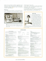
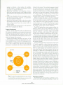
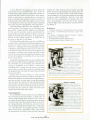
Fig. 4. Hybrid output stage uses discrete chips for drivers.
Fig. 3. Preamp chip has twenty-seven 2-GHz transistors.
emitters of Q26 and Q27.
The collectors of Q26and Q2 7 are connected to the
corresponding collectors of the other preamp chip
and to the input of a four-transistor delay-line driver.
This stage provides a current gain of 8 when driving
the 180ÃÃ differential delay line.
RT5 which constitute an attenuator with a 1-2-4 atten
uation sequence. Range selection in this section is ac
complished by grounding the lower end of resistor
R3, R4, orR5 to actuate the appropriate set of currentsource transistors (Q6-Q11).
During range selection, this section cycles four
times while the x 10 section cycles twice and the
external x 100 section once to give twelve attenua
tion ranges.
Output 1C
The output amplifier (U2 in Fig. 1) consists of a
25-mm square ceramic substrate with nine thick-film
resistors, one high-frequency monolithic chip con
taining six transistors, and two discrete transistor
chips for the final drive. The short signal paths af
forded by the thick-film hybrid technology plus the
performance of the HP transistors enabled these eight
transistors to achieve a differential voltage gain in
excess of 50 at a bandwidth of 150 MHz and with
differential drive capability of 70 mA.
Sync Extraction
The sync signal is extracted at the outputs of tran
sistors Q4 and Q5. As with other recent HP oscillo
scopes, sync extraction precedes the polarity and
gain vernier controls to prevent loss of triggering
when these controls are adjusted. Transistors Q17
and Q18 invert the sync signal when they are turned
on (and transistors Q15 and Q16 are turned off) by
transistors Q13 and Q14. To switch the sync signal
channel completely off, + 5V is applied to resistor R6.
Proceeding towards the output through buffer am
plifier Q19-Q20, the next control functions are the
gain vernier control and channel polarity. These two
functions are accomplished by a four-quadrant multi
plier configuration (Q22-Q25) that provides con
tinuously adjustable gain over a 2.5:1 range while
maintaining a constant dc bias current.
Channel switching is accomplished by doubleemitter transistor Q21. When the base potential on
this device exceeds the base voltages on transistors
Q22-Q25, it extracts and sums the currents that would
flow to transistors Q22-Q25. The collector current of
Q21 divides equally into the lower emitters of Q26
and Q27 so the channel bias current remains con
stant, maintaining the dc output level constant, but
all signal information is lost.
Position modulation is accomplished by differen
tially varying the bias currents injected into the upper
Acknowledgments
Ruth Buss, Gina Anderson, and Rose Stamps spent
many hours developing prototypes of the hybrid cir
cuits. Ken Fulton contributed to the special hybrid
processing procedures and Joe Cochran developed
the hybrid testing procedures. ^?
Joe K. Millard
A native of Maryville, Tennessee,
Joe Millard was involved with the
design and development of
nuclear instrumentation for seven
years at the Oak Ridge National
Laboratory (Tennessee) before
joining Hewlett-Packard in 1972.
He has BS, MS, and PhD degrees
from the University of Tennessee.
Married, and with two children,
Joe golfs, skis, and hikes during
leisure hours.
11
© Copr. 1949-1998 Hewlett-Packard Co.