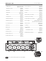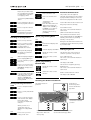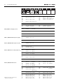
1
BeoSound 9000 MKIII
Type 2571, 2572, 2573, 2574, 2575, 2576, 2577, 2580
Service Manual
English, German, French
Survey of modules
1.1
1 FM/AM - RDS .......................................diagram A, AA, B, BB
page 2.11, 12, 13, 14
26 End Stop Detector ..............................................diagram M
page 2.28
3 Main Microcomputer ...........................................diagram J
page 2.24
27 Safety TX .............................................................diagram M
page 2.28
4 Mains Filter ......................................................... diagram N
page 2.29
28 Safety RX .............................................................diagram M
page 2.28
5 Mains Relay .....................................................diagram N, O
page 2.29, 30
29 Lamp ...................................................................... diagram I
page 2.23
7 Display ................................................................... diagram I
page 2.23
30 IR Transmitter, tacho clamper .............................. diagram I
page 2.23
9 Sledge Position ...................................................diagram M
page 2.28
31 IR Reciever, tacho clamper ................................... diagram I
page 2.23
11 Main Keyboard, right ......................................... diagram H
page 2.22
32 Input/output Select, Sound Adj. ................ diagram E, F, G
page 2.18, 19, 20
12 Main Keyboard, left ........................................... diagram H
page 2.22
34 Power Supply .......................... diagram C, D, G, H, I, J, L, N
page 2.16, 17, 20, 22, 23, 24, 26, 29
13 Secondary Keyboard .......................................... diagram H
page 2.22
35 Motor Control .................................................diagram L, M
14 IR Receiver ........................................................... diagram H
page 2.22
37 Lid Motor ............................................................diagram M
page 2.28
20 ML Interface ......................................................... diagram E
page 2.18
41 CD VAM 1250
CD .........................................................................diagram C
page 2.16
21 Headphone ......................................................... diagram G
page 2.20,
22 Clamper Position .............................................. diagram I, L
page 2.23, 26
24 Light Indication, left .............................................diagram J
page 2.26, 28
Turn Table Motor Control .................................. diagram D
page 2.17
95 CD Mechanism, VAM 1250 ............................. diagram C, D
page 2.16, 17
page 2.24
25 Light Indication, right ..........................................diagram J
page 2.24
30
4
20
1
32
21
35
13 3
5
24
31
29
37
34
9
7
25
26
14
27
12
11
28
22
41
= PCB13, PCB24 and PCB25 placed on the chassis topplate
95
1.2
Specification guidelines for service use
SPECIFICATION GUIDELINES FOR SERVICE USE
With FM and AM range and RDS
BeoSound 9000 MKIII
Type 2571 (EU), 2572 (GB), 2573 (USA-CDN), 2574 (J), 2575 (AUS),
2576 (TWN), 2577 (KOR), 2580 (LAT)
Operation
Direct keyboard
Beo4, BeoLink 1000
Mechanical functions
Change from playing CD1 to playing CD6
(Lid closed and known CD’s)
Position of CD
< 6.5 sec., typical 4 sec.
Typical ±1°
Tuner
Number of Programmes
Stereo / Mono selection
60
Automatic / manual
Tuner, FM section
Range
Aerial impedance
Usable sensitivity mono (30 dB)
50 dB quieting stereo
Signal-to-noise at 65 dBf mono
Signal-to-noise at 65 dBf stereo
Frequency response
Distortion + noise mono
Distortion + noise stereo
Intermodulation stereo
Stereo channel separation
Subcarrier product rejection
Tuner, AM section
Range
87.5-108 MHz
76-90 MHz f. type 2564
75 ohm
Typical 11dBf - 1µV
≤ 41dBf
≥ 69dB
≥ 64dB
20-15000Hz
≤ 0.6%
≤ 0.6%
Typical 0.1%
Typical 30dB
≥ 50dB
Antenna
LW sensitivity 20 dB S/N ratio
MW sensitivity 20 dB S/N ratio
Harmonic distortion
LW 153-279 kHz f. type 2571, 2572, 2575, 2576, 2577
MW 522-1611 kHz f. type 2571, 2572, 2575, 2576, 2577
MW 530-1710 kHz f. type 2573, 2580
MW 522-1629 kHz f. type 2574
Loop 18.1µH (Special)
Typical 66dBµV/m ( 2mV/m )
Typical 60dBµV/m ( 1mV/m )
Typical 0.4 %
CD Player
Number of CD’s
Disc types
Frequency range
Signal-to-noise ratio A-weighted
Dynamic range
Harmonic distortion
Channel separation
Channel difference
Converter system
6
12 cm (5”), 8 cm (3”) with adaptor
20-20.000 Hz ±1dB
Typical 101dB
≥ 98 dB
≤ 0.1%
≥ 50 dB
≤ ±1dB
Bitstream
Preamplifier section
Harmonic distortion
Frequency range ±1dB
Channel separation
Source separation
Signal-to-noise A-weight
Volume control
Bass control
Treble control
≤ 0.1%
10-20000Hz
≥ 50dB
≥ 80dB
≥ 90dB
≥ 90dB
7.0dB ±2dB at 100Hz
7.0dB ±2dB at 10kHz
Specification guidelines for service use
Connections
Master Link
Pin 1
Pin 2
Pin 3
Pin 4-6
Shield
Data-, -0.5 V ±0.2 V in relation to Data+
Data+, +0.5 V ±0.2 V in relation to DataML connect > 3 V
+supply voltage, +7 V to +15 V
(in stand-by +3 V to +15 V)
Not used
-supply voltage, -7 V to -15 V
(in stand-by -2 V to -15 V)
+supply voltage, +7 V to +15 V
(in stand-by +3 V to +15 V)
Audio L- in/out, 2 V Bal, in relation to Audio L+,
Rin 4.4 MW, Rout 150 Ω
Audio L+ in/out, 2 V Bal, in relation to Audio L-,
Rin 4.4 MW, Rout 150 Ω
Audio R- in/out, 2 V Bal, in relation to Audio R+,
Rin 4.4 MW, Rout 150 Ω
Audio R+ in/out, 2 V Bal, in relation to Audio R-,
Rin 4.4 MW, Rout 150 Ω
GND
Power Link
Pin 1
Pin 2
Pin 3
Pin 4
Pin 5
Pin 6
Pin 7
Pin 8
Power up (ON = >2.7 V -1mA)
Signal GND
Audio L out 0 V to 2 V RMS
Speaker ON (ON = >2.7 V -1 mA)
Audio R out 0 V to 2 V RMS
Datalink out (High = >4 V, Low = <0.2 V)
Data GND
PL+ ON
Audio Aux Link
Pin 1
Pin 2
Pin 3
Pin 4
Pin 5
Pin 6-7
Audio L out 1 V RMS, Rout 1 kΩ
GND
Audio L in 0.25 V RMS to 2 V RMS, Rin 47 kΩ
Audio R out 1 V RMS, Rout 1 kΩ
Audio R in 0.25 V RMS to 2 V RMS, Rin 47 kΩ
Not used
Headphones
Ø 3.5 mm, 220 W
Digital output CD
AES / EBU
IEC 958
0.5Vpp, 75W, 1%
Mains
Cable included
Type 2571, 2572, 2577, 2580 – 230V AC
Type 2573, 2576 – 120V AC
Type 2574 – 100V AC
Type 2575 – 240V AC
Power frequency
50-60 Hz
Power consumption Stand.by
Power consumption
Typical 1.0W
Typical 15W
Pin 7-10
Pin 11
Pin 12
Pin 13
Pin 14
Pin 15
Pin 16
1.3
1.4
Specification guidelines for service use
Dimensions
WxHxD
Weight
Finish
86.9 x 7 x 30.1 cm
11.5kg
Black, aluminium
Optional accessories
Beo4
Wall bracket horizontal
Wall bracket vertical
Bracket
Stand, adjustable in two heights
Cable cover
AM loop antenna
FM antenna
Type 1624, 1625 (I)
Type 2054
Type 2063
Type 2053
Type 2065
Type 2062
8720047
8720048
Type
Transformer
2571 EU
2572 GB
2573 US
2574 JAP
2575 AUS
2576 TWN
2577 KOR
2580 LAT
8013551 EU-230V AC
8013551 EU-230V AC
8013549 US-120V AC
8013548 JAP-100V AC
8013550 AUS-240V AC
8013549 US-120V AC
8013551 EU-230V AC
8013551 EU-230V AC
Subject to change without notice
PCB5
Mains Relay
8005661 EU
8005661 EU
8005664 US
8005661 EU
8005661 EU
8005664 US
8005661 EU
8005661 EU
PCB34
Power Supply
8000512 EU
8000512 EU
8000536 US
8000512 EU
8000512 EU
8000536 US
8000512 EU
8000512 EU
PCB1
FM/AM
8000462 EU
8000462 EU
8000462 EU
8000535 JAP
8000462 EU
8000462 EU
8000462 EU
8000462 EU
Mains cable
6100273
6100329
6100307
6100331
6100332
6100307
6100386
6100273
Brief operation guide
BRIEF OPERATION GUIDE
For more detailed operation see
User’s guide.
Programming a series of tracks
for one CD
1.5
Repeat this procedure for all
the CDs you have loaded…
Press to play CD
Closeup operation:
Press to scan the CD
[EDITING?] appears on the
display
Loading CDs
then
Press to start scanning the
tracks
Press to raise the glass door
If you want to clear the positions for a CD, move the carriage to the CD in question…
then
then
Press to clear the position
Press to lower the glass door
Press to include a track
number in the series
or
Press to lower the door and
start playing
or
Naming CDs
Press to exclude a track
number from the series
[EDITING OK] appears on the
display when you have
included or excluded the last
track…
Press to play a CD
Press to access the naming
function
then
or
then
Press to accept the track
series
or
Press to play the same track
again or press twice to play
the previous track
Press to play CD
then
CD playback
Press to play the next track
on a CD
Press to access the positioning
function to clear the position
Press to reveal the characters
or numbers one by one
then
Press to move to next
character position
To clear a track series…
then
Press to store the name
Choose the CD whose track
series you want to clear
Press to pause playback
Press while you are naming
CDs or track series in order
to automatically store the
name and exit the naming
function
then
Press to access the programming option
Press to resume playing
then
Press to clear the track series
altogether
Random
Press to display [RANDOM
ON] and cut in the random
play function
To clear a name, follow this procedure…
Playing edited CDs
Press to access the naming
function
Press to start playback of a CD
then
Press twice to display
[RANDOM OFF] and cancel
the random play function
Press to clear the name
then
Press to switch to stand-by
Press to display [EDIT ON]
and start edited playback
then
Press twice to play a CD in
full and cancel EDIT – [EDIT
OFF] appears on the display
Listing CDs
Press to return to normal
source operation
Press to play CD
Choosing a sequence of discs
Press to start playback of a CD
Positioning CDs
then
Load and adjust a CD manually…
Press SELECT and [SELECT
DISC] will appear on the
display
Then press the direct CD
selection button next to this
CD to move the carriage to
the CD …
Press the direct CD selection
buttons next to the CDs you
want to include…
then
Press to clear the sequence
then
Press to list the names one
by one and return to names
further up the list
Press to access the
positioning function for CDs
Press to clear a name while
the appropriate name is
displayed
Press to store the position
for this CD
Press to return to normal
source operation
then
Press SELECT to start clearing
a sequence and play all six
CDs
or
Press to access the naming list
[CD LIST] appears briefly,
then the name of the current
CD appears
then
1.6
Brief operation guide
Playing your radio programs
Mono/stereo reception
Press to turn on the radio
or
Press to step through your
radio programs
Playing auxiliary sources
Press to turn on the relevant
radio program
then
Press to choose [MONO] or
[STEREO]
Press to select extra
equipment
Adjusting sound
Press to raise the volume
then
Press to switch to stand-by
then
or
Press to lower the volume
Press to switch from stereo
to mono
Press to access treble
Presetting radio stations
Press to access bass
Press to store your new tuning on the program number
Press to turn on the radio
Press to start the tuning
function
Press to select [AM] or [FM],
switches from one to the
other, check display for an
indication of which one you
have chosen
Clearing presets...
Press to access balance
or
Press to turn on the radio
or
Press to search for program
number
Press to see the status of the
loudness adjustment function
– [LOUDNESS ON] or [LOUDNESS OFF]. Press LOUDNESS
again to change the setting
then
or
Press to search for a radio
station up or down the
frequency band
Press to clear the program
then
Press to accept all sound
levels - [SOUND OK?]
appears on the display
Press to confirm the clearing
of the radio program
then
Press to accept the station
you have found
then
Naming radio programs
Press to change the displayed
program number
Press to turn on the radio
program you want to name
Press to select for a program
number – up or down
Press to start the naming
function.
The first of the twelve character positions blinks, indicating that you can start
“writing” a name
then
or
then
Press to store your new radio
program – [STORED] appears
on the display
Press to store all sound levels
If you have not stored your
sound adjustments...
Press to reset the sound
levels to their previously
stored settings
Switching displays, example
or
Fine tuning a radio station
Press to reveal the characters
one by one
Press to reveal previously
shown characters
Press to turn on the radio
Press repeatedly to change
the radio display indication
then
Press to turn on the radio program you want to fine tune
Press to move to the next
character position
then
then
Press to start the fine tuning
function
Press to store the name of
the radio station [NAMING
OK] will appear on the display
or
or
Press to store the name and
exit the naming function
You can press RADIO at any
time to store and exit the
naming function
Press to fine tune your
program towards a higher or
lower frequency
then
Press to accept your fine
tuned program
Programming Timers
Press to start programming
timers
then
or
Press to accept the Timer
Then program when you
want the Timer to start and
stop…
To clear a name…
then
Press to access the naming
function
Press to clear the name
Press to choose a source for
your Timer or choose a Timer
stand-by
then
then
Press again to store program
and program number
Press to raise or lower the
treble and bass levels; or
adjust the balance between
the left and the right speaker
or
Press repeatedly until you
have found the exact time
for starting a Timer play
then
Press to accept start
Brief operation guide
Repeat the procedure with
the ▲ and ▼ buttons and OK
to program the exact timer
for stopping a Timer
Automatic demonstration
Press to show the clock
Press to see the date and
year
To program a [SINGLE DATE]
Timer...
or
To display the clock
permanently…
Press when Date and Year is
displayed and change the
display to time and ON e.g.
[14:40 ON] – press again to
cancel the permanent
showing of the clock e.g.
[14:41 OFF].
Press to display the date you
want to program a Timer for
then
Press to accept the selection
then
Press to store your Timer
programming and return to
normal source operations
Checking or clearing Timers
Press to check your timers
then
or
Press to see timer programming number, source and
program number of
individual timer entries
Press repeatedly to display
the details of a particular
programming
1.7
Option programming Beo4
hold
while pressing
Until the Beo4 display reads
OPTIONS?
then
The product can be brought into
automatic demonstration mode in which
it plays back 90 randomly chosen tracks.
Each track is played back for 20 seconds.
Load six CD’s with at least ten tracks each.
Bring the product into stand-by.
Press: SHIFT 9 1 9 9 6.
The remote control terminal must be in
audio mode.
(SHIFT is found under LIST on Beo4)
The automatic demonstration can be
stopped by bringing BeoSound 9000 into
stand-by, which is done by actuating
stand-by on the product.
During the automatic demonstration the
sound will be muted. Demute the product
if you want sound.
Until the display reads A:OPT
Locking of glass lid
Disable the remote control
function
The glass lid can be locked so that it
cannot be operated on the product.
Enable the remote control
function
Press: SHIFT 9 0 3 6 9.
The remote control terminal must be in
audio mode.
then
or
When the display reads [OK ?]
then
or
Press to display [NEXT ?] to
see your next timer programming entry
then
Option programming
BeoLink 1000
Press to see your next entry –
If there are no more entries,
[NO MORE], will appear on
the display
The display reads: LOCK.
Disable the remote control
function
The function is stopped by pressing:
SHIFT 9 0 3 6 9.
The remote control terminal must be in
audio mode.
or
Press clear while information
regarding a timer programming is displayed on the
display – [CLEARED] will
appear on the display after
pressing CLEAR
Setting and using the built-in
clock
Enable the remote control
function
SHIFT is found under LIST on Beo4
The display reads: UNLOCK.
Centering the CD drive mechanism
The sledge must be in
Centered for a
position 1.
horizontal position.
Used for the bracket
Press to call up the built-in
clock
type 2053.
then
or
Press to set time, date/month
or year…
then
Press to accept the changes
and reveal the next display Repeat this setting
procedure for date/month
and year…
When you have set or
changed the year, the
display now reads [CLOCK
OK?]
then
Press to store your new
setting of the clock
Centered for a vertical
position.
Centered for a flat or near
Centered for a horizontal position.
flat position. This is the
Used for the bracket type 2054.
factory setup.
1.8
Brief operation guide
The PIN-code system
Activate the PIN-code system
Change or delete your PIN-code
Using your PIN-code
While the BeoSound 9000 is in stand-by
mode you can set up the PIN-code.
While the PIN-code function is turned on you
can always make changes to the PIN-code.
When a PIN-code has been programmed, and
the BeoSound 9000 has been disconnected
from the mains for more than 30 minutes, you
must enter the PIN-code when the BeoSound
9000 is turned back on.
p
p
PAUSE
NEW PIN
Press p twice followed
by PAUSE to activate
the PIN-code function.
The display shows NEW
PIN for 1.5 sec.…
p
p
PAUSE
Press p twice followed
by PAUSE to activate
the PIN-code function
PIN _ _ _ _
Enter the current PINcode. The display shows
NEW PIN?
NEW PIN?
PIN _ _ _ _
…then you can enter a
PIN-code
m
p
Press to select a digit*
OK
Press to accept the digit
m
p
NEW PIN?
PIN _ _ _ _
m
p
Press to select a digit
OK
Press to accept the digit
R ADIO 1
When the PIN-code has
been entered the
display returns to the
relevant source display
e.g. RADIO 1
Press to choose from
the two options NEW
PIN? or PIN OFF?
PIN OFF?
The digit is replaced by a * and the next underscore blinks. Continue to enter the last three digits
in the same manner.
Select NEW PIN? to change your PIN-code
PIN _ _ _ _
Enter the new PIN-code
OK
CONFIRM
If you wish to change the entered digits…
RESET
Press to start entering
from the beginning
PIN _ _ _ _
When the PIN-code has been entered…
OK
Press to accept the PINcode. The display shows
CONFIRM
CONFIRM for 1.5 sec.…
PIN _ _ _ _
OK
STORED
…then re-enter the PINcode
Press to confirm the PINcode
The display shows that
your setting is stored
If an incorrect code is entered the second time
you must set up the PIN-code from the beginning.
*NOTE!: It is also possible to enter the digits using
the number keys 0 – 9 on your Beo4 remote
control.
OK
STORED
Press to accept the new
PIN-code. The display
shows CONFIRM for 1.5
sec.…
…then re-enter the new
PIN-code
Press to confirm the
new PIN-code
Enter the PIN-code
If an incorrect PIN-code is entered the display will
show ERROR and you may try again. After the
fifth try, the BeoSound 9000 is turned off, and
must be left in stand-by mode for 3 hours, before
you can try again.
Did you forget your PIN-code?
Should you forget your PIN-code you can
require a five-digit Master Code from your
Bang & Olufsen retailer.
The display shows that
your new PIN-code is
stored
When you have received a Master Code…
Select PIN OFF? to delete your PIN-code
PIN _ _ _ _
When the display is
DELETED
The PIN-code function is
open for PIN-code
disabled and the display
input…
shows DELETED for 3 sec.
For security reasons it is only possible to change or
verify the PIN-code five times within a period of 3
hours. If an incorrect code is entered five times,
BeoSound 9000 is turned off, and must be left in
stand-by mode for 3 hours, before you may try
again.
p
PIN _ _ _ _ _
PIN _ _ _ _ _
Press the p button for
more than 3 seconds to
change the display to fit
5 digits
Enter the Master Code
m
p
Press to select a digit
OK
Press to accept the digit
DELETED
The display shows that
the PIN-code lock is off
When the Master Code is entered, the BeoSound
9000 can be used without entering the code
again.
Explanation of diagram
2.1
Explanation of diagram
Type numbers of transistors and ICs are indicated on the diagrams. If the position
is followed by an asterisk the spare part number must always be used because the
component in question has been specially selected, e.g. IC4*.
Component print and coordinate system
The largest PCBs have component prints and a coordinate system on both the
primary and the secondary side.
On the diagrams every component has a coordinate number.
This indicates in which coordinate on the PCB the component is situated. The
coordinate numbers are written in smaller print types than the position numbers.
= C27 is placed on the primary side in coordinate 1A.
= R10 is placed on the secondary side in coordinate 2B.
Control circuit
In certain control circuits the active mode is indicated by a function term or by an
abbreviation. This may be e.g. ST.BY. = low in the stand-by mode or ST.BY. = high
in the stand-by mode.
Wiring connections
The wiring connections on the diagrams are assembled in ‘bundles’.
The individual wires are provided with one of the following codes:
INTERNAL CONNECTION ON
ONE DIAGRAM PAGE
Internal connections on a diagram page are indicated by a number.
The bend of the wire indicates in which direction the other end of the wire is
found.
CONNECTION TO ANOTHER
DIAGRAM PAGE
DIAGRAM A
DIAGRAM C
A connection to another diagram page is indicated by a number as well as by a
letter of the diagram to which the connection leads.
Ground symbols
Three different ground symbols are used in the set.
= Ground
= Chassis
= Coarse ground
Symbol of safety components
When replacing components with this symbol, components with identical part
numbers must be used. The new component must be mounted in the same way
as the one replaced.
2.2
Explanation of diagram
Measuring conditions
All DC voltages have been measured in relation to ground with a voltmeter with
an input impedance of 10 Mohms.
The DC voltages are stated in volts (V), e.g. 0.7V.
All oscillograms and AC voltages have been measured in relation to ground with
an oscilloscope or a voltmeter with an input resistance of 1Mohm.
AC voltages are stated in millivolts (mV), e.g. 660mV.
Caution
The use of any controls, adjustments or procedures other than those specified
herein may result in hazardous radiation exposure.
The black and yellow label on the compact disc player serves as a warning that the
apparatus contains a laser system and is classified as a class 1 laser product. The
apparatus must be opened by qualified servicemen only.
CD laserdiode
Wavelength 780 nm ±20 nm, 30ºC
Effect
2 mW ±0.1 mW, 30ºC
Lithium battery
WARNING
Short-circuit and overcharging of some types of lithium batteries may result in a
violent explosion.
When replacing the lithium battery in this set, note the following:
Use only batteries of the same make and type as mentioned in this service manual
(see page 3.9).
Place the battery exactly like the old one.
Explanation of the fuse symbols used in the set
Replace with the same type 1 ampere 250 volts quick acting fuse.
Replace with the same type 2.5 ampere 250 volts slow acting fuse.
Explanation des symboles de fusible utilisés dans l’appareil
Remplacer par un fusible rapide de même type et de 1 ampères 250 volts.
Remplacer par un fusible retardè de même type et de 2.5 ampères 250 volts.
Wiring diagram
Wiring diagram
2.3
2.3
Wiring diagram
2.3
2.4
Block diagram
2.4
2.4
Block diagram
Overall block diagram
PCB01
A,AA B,BB
PCB41
34IC7
PCB03
J
34IC12
34IC10
PCB34
PCB22
Block diagram
Block diagram for AM
Block diagram for Frontend Tuner
2.5
2.5
Block diagram
2.5
2.6
Block diagram for CD
Block diagram
2.6
2.6
Block diagram
Block diagram
Block diagram for Input/Output Select
2.7
2.7
Block diagram
2.7
2.8
Block diagram for Data
Block diagram
2.8
2.8
Block diagram
Block diagram
2.9
2.9
Block diagram
2.9
Block diagram for Motor Control
41
41IC16
22IC1
22
22PE1
22IC1
22PE2
41TR2/3/PE1/
DISC IC6
DETECTOR
41IC1
22IC1
22PE3
22IC2
22IC2
22IC2
2.10
Block diagram for Power Supply
Block diagram
2.10
2.10
Block diagram
Diagram A
DIAGRAM A – Frontend tuner
PCB drawing for PCB1 see page 2.15
2.11
2.11
Diagram A
2.11
2.12
DIAGRAM AA – FM/AM detector
Diagram AA
PCB drawing for PCB1 see page 2.15
2.12
2.12
Diagram AA
Diagram B
DIAGRAM B – Stereo decoder and power section
PCB drawing for PCB1 see page 2.15
2.13
2.13
Diagram B
2.13
2.14
DIAGRAM BB – RDS and µP
Diagram BB
PCB drawing for PCB1 see page 2.15
2.14
2.14
Diagram BB
PCB drawing
PCB1, FM/AM - RDS – primary side
2.15
2.15
PCB drawing
PCB1, FM/AM - RDS – secondary side
2.15
2.16
DIAGRAM C – CD servo decoder
Diagram C
PCB drawing for PCB41 see page 2.17
2.16
2.16
Diagram C
Diagram D
DIAGRAM D – Turn table and motor control
2.17
2.17
Diagram D
2.17
PCB41, CD – primary side
PCB41, CD – secondary side
2.18
DIAGRAM E – Master Link interface data/audio
Diagram E
PCB drawing for PCB32 see page 2.21
2.18
2.18
Diagram E
Diagram F
DIAGRAM F – Digital/analog decoder
PCB drawing for PCB32 see page 2.21
2.19
2.19
Diagram F
2.19
2.20
DIAGRAM G – Input select and Sound adjustment
Diagram G
2.20
PCB drawing for PCB21 and PCB32 see page 2.21
2.20
Diagram G
PCB drawing
2.21
2.21
PCB drawing
PCB21, Headphone
PCB32, Input/output Select, Sound Adjustment – preliminary side
PCB32, Input/output Select, Sound Adjustment – secondary side
2.21
2.22
DIAGRAM H – Keyboard and IR Receiver
PCB13, Secondary Keyboard
PCB drawing for PCB14 see page 2.30
Diagram H
2.22
2.22
Diagram H
Diagram I
DIAGRAM I – Display and clamper position
PCB22, Clamper Position
PCB drawing for PCB7 see page 2.31
2.23
2.23
Diagram I
2.23
2.24
DIAGRAM J – Microcomputer, Power supply & Light Indicator
Diagram J
2.24
2.24
PCB drawing for PCB24 see page 2.30 – PCB34 see page 2.25
Diagram J
PCB drawing
PCB34, Power Supply
2.25
2.25
PCB drawing
2.25
2.26
DIAGRAM L – Motor Control
Diagram L
2.26
2.26
Diagram L
PCB drawing
PCB35, Motor Control
2.27
2.27
PCB drawing
2.27
2.28
PCB9, Sledge Position
PCB26, End Stop Detector
PCB28, Safety RX
PCB37, Lid Motor
Diagram M
2.28
DIAGRAM M – Motor Control and Detection
2.28
Diagram M
PCB drawing for PCB35 see page 2.27
Diagram N
DIAGRAM N – Power Supply
2.29
PCB drawing for PCB4 see page 2.31 – PCB5 see page 2.30 – PCB34 see page 2.25
2.29
Diagram N
2.29
2.30
DIAGRAM O – Mains relay USA
PCB14, IR Receiver
PCB24, Light indication, left
PCB drawings
2.30
2.30
PCB drawings
PCB5, Mains Relay
PCB drawings
PCB4, Mains Filter
PCB7, Display
2.31
2.31
PCB drawings
2.31
3.1
List of electrical parts
3.1
List of electrical parts
Resistors not referred to are standard, see page 3.13 and 3.14
PCB1, 8000462 FM/AM - RDS
Type 2571, 2572, 2573, 2575, 2576,
2577, 2580
∆ indicates that static electricity may
destroy the component
IC200∆
IC201∆
IC203∆
IC300∆
IC400∆
8344023
8343950
8342519
8343681
8343809
147
151
151
136
170
TDA7421N
TS912ID
M24C02
TDA7403D
MAX809
TR200
TR201TR202
TR203
TR204
TR400TR401
TR402
8320753
8321276
51
53
BC856B
BF1009S
8321277
8320936
8320856
75
51
68
HN3G01J
BC847C
2N7002-T1
8320778
51
BC857C
D200D203
D204D205
D400
8301140 252
BB914
8301143 267
BAR63-04
8300894
BAW56
69
R208
R209
R226
R231
R234
R235R236
R237
R238R239
5013156
5012331
5013152
5012238
5012238
5012331
2.2KΩ 1/16W
10KΩ 1/8W
1.2KΩ 50V
33KΩ 1/8W
33KΩ 1/8W
10KΩ 1/8W
C200
C201
C203
C204
C205
C206
C207
C208
C209C210
C211
C212
C213
C214C215
C216
C217
C218C219
C220
C221
4000404
4001127
4001121
4011122
4011134
4010419
4001125
4011134
4011135
22pF
22pF
6.8pF ±0.1pF 50V
10nF 50V
100nF 16V
4.7µF 10V
15pF 50V
100nF 16V
100nF 25V
4010434
4000404
4001113
4001125
4.7µF 16V
22pF 50V
1.5pF 50V
15pF 50V
5012238 33KΩ 1/8W
5012331 10KΩ 1/8W
4001143 470pF 50V
4001125 15pF 50V
4011135 100nF 25V
4001143 470pF 50V
4001120 5.6pF ±0.25pF
IC401∆
8344055 147
IC402∆
IC500∆
8342568 136
8343733 168
TR403TR404
TR500
TR501
TR502
TR503TR504
D401
D402
D500
D501
R240
R312
R316
R400R401
R419
R428
R517
C222C223
C224
C225
C226
C227C231
C232
C233
C234
C235
C236
C238
C239
C240
C241
C242
C243
C244
C245
C246
8320755
51
µPH8S2137
f/SW 1.5
SAA6579T
L4931ABPT80
BC847B
8320971 51
8320936 51
8321196 136
8320971 51
BC807-40
BC847C
PUMZ1
BC807-40
8300895
8300520
8301056
8301064
BAV70
BZX284-B6V8
BZX284-B2V7
Z5.1V BZX284
5012559
5011300
5011300
5011300
252
250
250
250
5.1KΩ 1/8W
180Ω 0.25W
180Ω 0.25W
180Ω 0.25W
5030051 1KΩ
6000059 Jumper
5021532 270Ω 0.25W
4001118 3.9pF ±0.1pF 50V
4011135
4001143
4001126
4011134
100nF 25V
470pF 50V
18pF 50V
100nF 16V
4010387
4010323
4010274
4011110
4010387
4000493
4000494
4000495
4000496
4010419
4011134
4000495
4010420
4001136
470nF 16V
1µF 16V
100nF 25V
1nF 50V
470nF 16V
1.2nF ±10% 50V
4.7nF ±10% 50V
3.3nF ±10% 50V
33nF ±10% 50V
4.7µF 10V
100nF 16V
3.3nF ±10% 50V
10µF 10V
120pF 50V
3.1
List of electrical parts
C247
C248C250
C251
C252C253
C254
C255
C256
C258
C259
C260C261
C262
C263
C264
C265
C266
C267
C268
C269C270
C271C272
C273
C274
C275
C276
C277
C278
C279
C281C282
C283C286
C288
C289C290
C291
C292C294
C295
C296
4011130 47nF 16V
4010420 10µF 10V
L200
L201
L202L203
L204
L205
L206
L207
L208
L209
L210
L211L212
8021078 Coil 1µH
8021319 Coil 97nH
8021320 Coil 97nH
4010316 100nF 25V
4011134 100nF 16V
4010421
4011134
4010316
4010274
4001135
4011122
1µF 16V
100nF 16V
100nF 25V
100nF 25V
100nF 25V
10nF 50V
4010419
4001130
4001133
4001130
4010322
4011134
4010420
4011134
4.7µF 10V
39pF 50V
68pF 50V
39pF 50V
4.7µF 16V
100nF 16V
10µF 10V
100nF 16V
4001127 22pF 50V
4001132
4001125
4001129
4000494
4010421
4010316
4011134
4000408
56pF 50V
15pF 50V
33pF 50V
4.7nF 50V
1µF 16V
100nF 25V
100nF 16V
47pF 50V
4010274 100nF 25V
4000494 4.7nF 50V
4010274 100nF 25V
4011134 100nF 16V
4011122 10nF 50V
4001143 470pF 50V
4011135 100nF 25V
8021318
8021374
8021321
8021325
8021323
8020909
8021324
8020626
Coil 71nH
Transformer 10.7MHz
Coil 10.7MHz
Coil 1mH 1%
Transformer 450kHz
Transformer 330mH
Coil 10uH
Coil 470uH
BP200
BP201BP203
8030391 Cer. filter 450KHz
8030400 Cer. filter 10.7MHz
X200
8090274 Crystal 10.25MHz
F500
6604039 Fuse 200mA
FE200FE201
6710060 Ferrite
P101
P103
7221373 Male connector
7211221 Socket 4 pole
C298
C300
C301
C302
C303
C304
C305
C306
C307
C309C310
C311
C312
C313
C314C317
C318
C400
C401
C402
C403
C404C407
C408
C409
C410
C411
C412
C413
C414
C415
C416
C417
C418
C419
C420
C421
C422
C502
C503
C505
C506
C507
4010420
4010419
4011128
4011120
4011130
4010421
4010435
4010419
4011134
4010420
10µF 10V
4.7µF 10V
33nF 25V
6.8nF 50V
47nF 16V
1µF 16V
10µF 25V
4.7µF 10V
100nF 16V
10µF 10V
4010237
4011110
4010237
4011110
1nF 50V
1nF 50V
1nF 50V
1nF 50V
4001138
4011110
4010321
4011122
4010237
4001131
180pF 50V
1nF 50V
470nF 16V
10nF 50V
1nF 50V
47pF 50V
4010321
4011110
4011056
4001134
4011122
4011110
4001141
4011122
4010419
4011122
4001143
4001131
4001134
4011110
4010321
4010316
4010434
4010316
4010315
4011122
470nF 16V
1nF 50V
1nF 50V
82pF 50V
10nF 50V
1nF 50V
330pF 50V
10nF 50V
4.7µF 10V
10nF 50V
470pF 50V
47pF 50V
82pF 50V
1nF 50V
470nF 16V
100nF 25V
4.7µF 16V
100nF 25V
22nF 50V
10nF 50V
L213L214
L215
L216L217
L218
L301L302
L303
L400L404
L500L501
8020714 Coil 68uH
X400
8090206 Crystal 8.664MHz
P106
P107
7211222 Socket 6 pole
7221082 Plug 2 pole
6000064 Jumper
8020821 Coil 2.2uH
8021366 Transformer
6000064 Jumper
8021345 Coil 10mH
8020821 Coil 2.2uH
6000064 Jumper
List of electrical parts
PCB1, 8000535 FM/AM - RDS
Type 2574
C202
C203
C213
C221
C222C223
4000401
4001125
4001120
4001126
4001119
12pF 50V
15pF 50V
5.6pF 50V
18pF
4.7pF 50V
L201
L202L203
L204
8021385 Coil 108nH
8021384 Coil 108nH
C274
C275
C297
3.2
4001127 22pF 50V
4001131 47pF 50V
4000401 12pF 50V
8021350 Coil164nH
Other electrical parts like PCB1, type 2571, 2572, 2573, 2575, 2576, 2577, 2580
PCB3, 8000513 Main Microcomputer
IC3∆
8343945 147
PCB4, 8000463 Mains Filter
L1
8022318 Coil 2 x 3.3mH
P85P86
7221057 Plug 2/3 pole
D1D2
D3
8300915 209
GF 1M
8301045 250
BAS216
C1
4200821 1000µF -20+50% 6.3V
RL1
7600120 Relay 5V
F1
6600084 Fuse 100mAT 250V
P82
P83
P84
7221057 Plug 2/3 pole
7211221 Socket 4 pole
7221163 Plug 4/3 pole
R1
5000194 3.3MΩ 10% 1/2W
F1
6600164 Fuse 100mAT 125V
PCB5, 8005661 Mains relay
Type 2571, 2572, 2574, 2575,
2577, 2580
PCB5, 8005664 Mains relay
Type 2573, 2576
SW IC
Other electrical parts like PCB5, type 2571, 2572, 2574, 2575, 2577, 2580
PCB7, 8005364 Display
symbol of safety component, see page 2.1
∆ indicates that static electricity may
destroy the component
74HC138
TIMER 555
4013
SI9958DY
IC8∆
IC50∆
IC51∆
IC52∆
8341277
8341857
8340433
8341812
138
138
138
138
74HC14
LM339
74HC86
LM393
BC847B
TR53
8320811
51
BC857B
8300606 250
8300907 256
LL4448
GF1B
8300606 250
8300606 250
8300606 250
8330387 265
8300606 250
Led red
LL4448
D13
D15
D50D55
C10C11
C12C13
C14C15
C16
4201448 330µF 20% 6.3V
IC1∆
IC2∆
IC3∆
IC4∆IC5∆
8342095
8342270
8340740
8342681
138
138
138
138
TR50
8320755
51
D1
D2D3
D4
D5D6
R59
5013256 39KΩ 1% 1/16W
C1C3
C4
C5
C6
C7
C8C9
4010274- 100nF -20+80% 25V
4010272
4010274
4010314
4010315
4010321
22nF -20+80% 50V
100nF -20+80% 25V
220nF -20+80% 25V
22nF 10% 25V
470nF -20+80% 16V
LL4448
LL4448
LL4448
4010321 470nF -20+80% 16V
4001143 470pF 5% 50V
4001135 100pF 5% 50V
➩
3.3
List of electrical parts
Resistors not referred to are standard, see page 3.13 and 3.14
PCB9, 8005312 Sledge position
PCB11, 8005295 Main keyboard, right
PCB12, 8005296 Main keyboard, left
PCB13, 8005313 Secondary keyboard
PCB14, 8005299 IR Receiver
∆ indicates that static electricity may
destroy the component
C17C18
C20C21
C22
4001143 470pF 5% 50V
IL1
8230125 Bulb, 190mA 6.3V
P62
P63
7211134 Socket 6 pole
7210893 Socket 12 pole
PE1∆
8330388
R1R2
5011853 158Ω 1% 1/4W
P78
7211221 Socket 4 pole
S1S4
7400429 Switch 1 pole
P97
7211136 Socket 4 pole
S1S4
7400429 Switch 1 pole
P72
P98
7211054 Socket
7211136 Socket 4 pole
IC1∆
IC2∆
8342095 151
8342297 151
74HC138
74HC147
TR1
8320755
BC847B
C1C2
C4
4010316 100nF 10% 25V
P71
7211057 Socket 12 pole
TR1
TR2
TR3
TR4
8321278
8320740
8321187
8321188
D33D36
D37
R7
C1
C2
C3
C4
C5
C23
C50
C51C52
4001135 100pF 5% 50V
4010274 100nF -20+80% 25V
4010323 1µF -20+80% 16V
P68
P69
7210889 Socket 4 pole
7211133 Socket 5 pole
BC849CW
BF840
BC846BW
BC856BW
TR5
TR6TR7
8320740
8321187
8301045 250
BAS216
D38D39
8330393 244
8330145 244
IR detector
880nm 455KHz
5011303 470Ω 5% 1/4W
R23
5021512 220Ω 1% 1/4W
4011134
4001143
4010334
4001131
4001143
C6
C7
C8
C10
C11
4001131
4000442
4010387
4001143
4001131
4001135 100pF 5% 50V
4010274 100nF -20+80% 25V
TCVT1300
51
4010271 10nF 10% 50V
51
51
51
100nF 10% 16V
470pF 5% 50V
220nF 10% 16V
47pF 5% 50V
470pF 5% 50V
51
51
BF840
BC846BW
IR detector 880nm
BPW34FAS
47pF 5% 50V
2.2nF 5% 50V
470nF 10% 16V
470pF 5% 50V
47pF 5% 50V
List of electrical parts
PCB20, 8001824 ML interface
PCB21, 8005301 Headphone
PCB22, 8000514 Clamper position
∆ indicates that static electricity may
destroy the component
C12C13
C14
4001143 470pF 5% 50V
4001131 47pF 5% 50V
L1
8020744 Coil 455KHz
BP1
8030392 Cer. filter 455KHz
P49
7211053 Socket 4 pole
IC1∆IC7∆
8341022 151
TR3
TR4TR5
8320811
8320755
R2
R4
R5R6
R8
R10
R11R12
5011841 11.8KΩ 1% 1/8W
5011841 11.8KΩ 1% 1/8W
5011531 5.9KΩ 1% 1/8W
C1C2
C3C4
C6C7
4000277 22pF 5% 50V
C1C2
3.4
C15
C20
C21
4011134 100nF 10% 16V
4011124 15nF 10% 50V
4011110 1nF 10% 50V
4558
IC8∆IC10∆
8341024 151
4066
BC857B
BC847B
TR6
8320811
BC857B
R14R15
R19R20
R23R26
5011557 10KΩ 1% 1/8W
C11C14
C100C101
4010166 100nF -20+80% 50V
4011110 1.0nF 10% 50V
C3C4
4010271 10nF 10% 50V
P1
7210510 Jack socket
P80
7211221 Socket 4 pole
IC1IC2
8341041 151
LM324
TR1
8320755
BC847B
PE1PE3
8330478 257
R1
R8
R15
R23
R24
5011188
5011188
5011188
5012278
5012316
R25
R28
R29R30
R33
5012366 20KΩ 1% 1/8W
5012239 39KΩ 1% 1/8W
5012290 4.87KΩ 1% 1/8W
C1
C4C5
C6
C7
C8C9
4010271 10nF 10% 50V
4010274 100nF -20+80%
C10
C11
C12
C13
C14
C15
4010237
4000415
4010237
4000412
4010237
4000412
P60
P61
P64
7211234 Socket 12 pole
7211340 Socket 6 pole
7221272 Plug 2 pole
51
51
5011841 11.8KΩ 1% 1/8W
5011841 11.8KΩ 1% 1/8W
5011531 5.9KΩ 1% 1/8W
4000241 100pF 5% 50V
51
5011557 10KΩ 1% 1/8W
5011571 75Ω 1% 1/8W
4000345 1.0nF 5% 50V
4000241 100pF 5% 50V
51
Optocoupler
330Ω 5% 1/4W
330Ω 5% 1/4W
330Ω 5% 1/4W
240KΩ 1% 1/8W
56.2KΩ 1% 1/8W
4010237 1nF 10% 50V
4010263 2.2nF 10% 50V
4010272 22nF -20+80% 50V
5012366 20KΩ 1% 1/8W
1nF 10% 50V
180pF 5% 50V
1nF 10% 50V
100pF 5% 50V
1nF 10% 50V
100pF 5% 50V
3.5
List of electrical parts
Resistors not referred to are standard, see page 3.13 and 3.14
PCB24, 8005304
Light indication, left
TR1TR6
8320755
51
BC847B
D4D6
8330387 230
Led red
P73
P74
6276998 Plug 8 pole
6276913 Plug 4 pole
PCB25, 8005305
Light indication, right
D1D3
8330387 230
Led red
PCB26, 8005315 End stop detector
IC1∆
8342715 164
A3141ELT
C1
C2
4010274 100nF -20+80% 25V
4010323 1µF -20+80% 16V
P75
P96
7211054 Socket 6 pole
7211053 Socket 4 pole
PCB27, 8005377 Safety TX
D1
8330266 245
TSHA4480
PCB28, 8005303 Safety RX
TR1
TR2
8330363
8320755
BPW77
BC847B
C4
4010323 1µF -20+80% 16V
IL1
8230125 Bulb, 190mA 6.3V
PCB32, 8005399
Input/Output select and sound adj.
IC1∆IC2∆
IC3∆
IC4∆
IC6∆
IC7∆IC10∆
8341025 138
4094
8341059
8342238
8340205
8341022
138
151
151
138
* specially selected or adapted sample
TR1
TR2
TR3
TR6
8320512
8320523
8320755
8320755
18
18
51
51
PCB29, 8005309 Lamp
74
51
PCB30, 8001865
IR transmitter, tacho clamper
PCB31, 8001866
IR receiver, tacho clamper
∆ indicates that static electricity may
destroy the component
4052
TDA7318D
LF347
4558
IC12∆
IC400∆
IC401∆
IC402∆
IC500∆*
IC600∆*
8341022
8342869
8342497
8342950
8342500
8342900
138
151
151
151
151
151
BC338-25
BC328-25
BC847B
BC847B
TR15TR18
TR19TR26
8320941
8320941
8321080
51
51
51
4558
CS8412
TDA1305
EL2045CS
Asic-ML Data
Asic-PL Data
2SC4213
2SC4213
FMMT491A
List of electrical parts
TR27TR28
TR29
TR400TR401
TR402TR404
8320755
51
BC847B
8320811
8321171
51
75
BC857B
FZT790A
8320755
51
BC847B
D2D3
D4D5
D10D14
D15D16
D17D18
8300644 250
Z6.2V 2% 0.5W
8301045 250
BAS216
8301045 250
BAS216
8300636 250
Z7.5V 5% 0.5W
8300723 250
Z8.2V 2% 0.5W
R141R148
R194R201
R250
R251
R253
R254
R400
R406R409
R425
5012331 10KΩ 1% 1/10W
C1C4
C5C6
C7C14
C17C22
C33C38
C41C42
C43
C45C46
C49C50
C51C52
C53
C54
C56
C59C64
C66C71
C73
C74C79
C82C85
C86C89
C90C107
C108C109
C110
C111C112
5012331 10KΩ 1% 1/10W
5012290
5012297
5012290
5012297
5021391
5021524
4.87KΩ 1% 1/10W
5.62KΩ 1% 1/10W
4.87KΩ 1% 1/10W
5.62KΩ 1% 1/10W
75Ω 1% 1/4W
47Ω 1% 1/4W
3.6
TR405
TR500
TR600
TR601TR602
TR603
8320811 51
8321159 51
8321198 136
8321197 136
BC857B
FMMT489
PUMX1
PUMT1
8321202
PDTC114EU
D19
D20D21
D400
D500D505
D600D601
8300762 250
8301045 250
Z9.1V 2% 0.5W
BAS216
8300563 250
8301045 250
Z5.1V 2% 0.5W
BAS216
8300520 250
Z6.8V 5% 0.5W
R505
R600
R602
R604
R605
R606
R607
R608
R609
R610
R611
5011599
5021484
5021484
5030052
5030054
5030052
5030050
5030053
5030050
5030055
5030054
C113C114
C116
C130
C131
C132
C133
C134C135
C150
C400
C401
C402
C403
C404
C405C406
C407C408
C411
C412C414
C415C416
C417C422
C500
C501
C502
C503
C504
C505C507
C600
C601C602
C603
C604
4201164 47µF 20% 10V
51
49.9KΩ 1% 1/8W
100Ω 1% 1/4W
100Ω 1% 1/4W
4 x 4.7KΩ 5% 1/16W
4 x 100KΩ 5% 1/16W
4 x 4.7KΩ 5% 1/16W
4 x 10KΩ 5% 1/16W
4 x 47KΩ 5% 1/16W
4 x 10KΩ 5% 1/16W
4 x 180KΩ 5% 1/16W
4 x 100KΩ 5% 1/16W
5013223 68Ω 1% 1/16W
4000420 470pF 5% 50V
4000351 1.5nF 5% 50V
4000408 47pF 5% 50V
4000412 100pF 5% 50V
4000416 220pF 5% 50V
4000424 1nF 5% 50V
4010237 1.0nF 10% 50V
4000424 1nF 5% 50V
4010237 1.0nF 10% 50V
4000424 1nF 5% 50V
4010237
4010271
4010271
4010271
1.0nF 10% 50V
10nF 10% 50V
10nF 10% 50V
10nF 10% 50V
4010271 10nF 10% 50V
4010271 10nF 10% 50V
4010274 100nF -20+80% 25V
4010274 100nF -20+80% 25V
4130307 150nF 10% 63V
4200916 4.7µF 20% 25V
4010271 10nF 10% 50V
4000281 82pF 5% 50V
4201163 10µF 20% 35V
4201391
4000414
4000457
4000414
4000457
4010271
10µF 20% 50V
150pF 5% 50V
1.5nF 5% 50V
150pF 5% 50V
1.5nF 5% 50V
10nF 10% 50V
4200972
4000408
4010274
4010273
4010274
4201164
4000424
4.7µF 20% 10V
47pF 5% 50V
100nF -20+80% 25V
47nF -20+80% 50V
100nF -20+80% 25V
47µF 20% 10V
1nF 5% 50V
4010274 100nF -20+80% 25V
4201348 1µF 10% 16V
4010274 100nF -20+80% 25V
4201163 10µF 20% 35V
4010274 100nF -20+80% 25V
4010237
4000416
4000412
4010316
4010274
4201163
1.0nF 10% 50V
220pF 5% 50V
100pF 5% 50V
100nF 10% 25V
100nF -20+80% 25V
10µF 20% 35V
4010274 100nF -20+80% 25V
4010132 1.0nF 10% 50V
4000408 47pF 5% 50V
4000416 220pF 5% 50V
3.7
List of electrical parts
Resistors not referred to are standard, see page 3.13 and 3.14
PCB34, 8000512
Power Supply
Type 2571, 2572, 2574, 2575, 2577,
2580
∆ indicates that static electricity may
destroy the component
L5L6
8020821 Coil 2.2µH 5%
P22
P23
P24
P26
P27
7211227
7500296
7211221
7221272
7221181
74HC4538
LM393
LM3578
IC7∆
IC10∆
IC14∆
8343333 138
8342397 138
8343330 138
4094B
M41T56M6
74HC138
8321198 136
PUMX1
8321187 51
8321188 51
8321187 51
8320936 51
8321198 136
8320740 51
BC846BW
BC856BW
BC846BW
BC847C
PUMX1
BF840
8321193 75
8321198 136
8321171 52
8321198 136
8321193 75
8321198 136
8320856 68
FZT788B
PUMX1
FZT790A
PUMX1
FZT788B
PUMX1
2N7002
8321363
8321188
8321187
8320936
8321363
8321188
8320752
8321187
8321363
8321188
8320936
8321187
8320740
STD10PF06
BC856BW
BC846BW
BC847C
STD10PF06
BC856BW
BC817-40
BC846BW
STD10PF06
BC856BW
BC847C
BC846BW
BF840
TR32
TR33
TR34
TR35
TR36
TR37
TR38TR40
TR41
TR42
TR43
TR44
TR46
TR47
TR48
TR49
TR50TR53
TR54
TR55TR57
TR58
TR59TR60
8321188 51
8320740 51
8321188 51
8320740 51
8321188 51
8321187 51
8321198 136
8321193 75
8321187 51
BC856BW
BF840
BC856BW
BF840
BC856BW
BC846BW
PUMX1
FZT788B
BC846BW
8321188
8321187
51
51
BC856BW
BC846BW
8321188
8321187
51
51
BC856BW
BC846BW
D15
D17
D19
D20
D21
D22D23
D24
D25
D27
D28
D29
8301061
8301045
8301072
8301217
8301104
8301045
256
250
256
250
250
250
Z3.9V 2% 0.4W
BAS216
Z10V 2% 0.4W
STPS3L60S
SM6T15C
BAS216
8301218
8301045
8301072
8301217
8301045
256
250
256
250
250
BAT254
BAS216
Z10V 2% 0.4W
STPS3L60S
BAS216
L1L4
8020705 Coil 100µH 10%
T400
8021159 Transformer 796KHz
P1
P2P3
P4
P20
P21
7210418 Socket 7 pole
7210689 Socket 8 pole
IC1∆
IC2∆
IC3∆IC5∆
8343327 138
8341812 138
8342673 151
TR1TR2
TR3
TR4
TR5
TR6
TR7
TR8TR9
TR10
TR11
TR12
TR14
TR15
TR16
TR17
TR20
TR21
TR22
TR24
TR25
TR27TR28
TR30
TR31
8321193 75
8321198 136
FZT788B
PUMX1
D1
D2
D3
D4
D5
D8
D9
D10
D11
D12
D13
D14
8300949
8301045
8301072
8301061
8301045
8301072
8301217
8301103
8301045
8301061
8301218
8301064
Bridge
BAS216
Z10V 2% 0.4W
Z3.9V 2% 0.4W
BAS216
Z10V 2% 0.4W
STPS3L60S
SM6T7V5CA
BAS216
Z3.9V 2% 0.4W
BAT254
Z5.1V 2% 0.4W
7210904 Socket 16 pole
7211221 Socket 4 pole
7211223 Socket 8 pole
69
51
51
51
69
51
51
51
69
51
51
51
51
250
256
256
250
256
250
250
250
256
256
256
Socket 16 pole
Contact pin
Socket 4 pole
Plug 2/2 pole
Plug 2 pole
List of electrical parts
D30
D31
D33
D34
8301218
8301217
8301059
8301104
256
250
256
250
BAT254
STPS3L60S
Z3.3V 2% 0.4W
SM6T15C
R4
R5
R7
R17
R18
R19
R20
R25R28
R36
R38R39
R40R41
R44
R47R49
R54
R61
R62R65
R66
R67
R70R71
R75
R88
5030054
5021508
5021508
5012382
5023035
5023052
5012175
5021542
4 x 100KΩ 5% 1/16W
47KΩ 1% 1/4W
47KΩ 1% 1/4W
10KΩ 0.1% 1/4W
560KΩ 1% 1/4W
470KΩ 1% 1/4W
43.2KΩ 1% 1/4W
0.22Ω 5% 1/4W
C1C4
C5
C6C7
C8
C9
C10
C11
C12
C13
C14C15
C16
C17
C18C19
C21
C22
C23
C24
C25
C26
C27
C28
C30
C31
C32
C33
C34
C35
C37
C38
C39
C40
C41
C42
4010216 22nF 10% 100V
5012200 2.2KΩ 1% 1/4W
5021484 100Ω 1% 1/4W
5012200 2.2KΩ 1% 1/4W
5030054 4 x 100KΩ 5% 1/16W
5021508 47KΩ 1% 1/4W
5030054 4 x 100KΩ 5% 1/16W
5012382 10KΩ 0.1% 1/4W
5021542 0.22Ω 5% 1/4W
5011843 80.6KΩ 1% 1/4W
5021225 10KΩ 1% 1/4W
5021484 100Ω 1% 1/4W
5030051 4 x 1KΩ 5% 1/16W
5030054 4 x 100KΩ 5% 1/16W
4201179 15000µF 20% 50V
4010216 22nF 10% 100V
4201406
4201163
4010216
4011135
4010216
4201178
4011122
330µF 20% 50V
22µF 20% 6.3V
22nF 10% 100V
100nF -20+80% 16V
22nF 10% 100V
8200µF 20% 10V
10nF 10% 50V
4201163 22µF 20% 6.3V
4001127 22pF 5% 50V
4011122 10nF 10% 50V
4011122
4000442
4010216
4001131
4011135
4201163
4010216
4201407
4011122
4001127
4010220
4011135
4200916
4000442
4010216
4201348
4201407
4011122
4011110
4201254
10nF 10% 50V
2.2nF 5% 50V
22nF 10% 100V
47pF 5% 50V
100nF -20+80% 16V
22µF 20% 6.3V
22nF 10% 100V
820µF 20% 25V
10nF 10% 50V
22pF 5% 50V
100nF 10% 50V
100nF -20+80% 16V
4.7µF 20% 25V
2.2nF 5% 50V
22nF 10% 100V
1µF 10% 16V
820µF 20% 25V
10nF 10% 50V
1nF 10% 50V
33µF 20% 16V
3.8
D40D46
D47
8301045 250
BAS216
8301061 256
Z3.9V 2% 0.4W
R92
R93
R94
R95R97
R100
R102R103
R114
R141
R143
R146
R154
R155
R161
R171
R187
R192
R195
R209
R210R211
R234
R245
R336
R339
5012382
5012169
5023032
5021542
C43C44
C45
C46
C47
C48
C49
C50
C51
C52
C53
C54
C55
C56
C57
C58C59
C61
C63
C66
C71
C76
C79
C80
C82
C86
C87
C92
C98
C99
C102
C103
C104
C108
C111
C112
C113
4011110 1nF 10% 50V
10KΩ 0.1% 1/4W
220KΩ 1% 1/4W
3.3MΩ 1% 1/4W
0.22Ω 5% 1/4W
5013172 105KΩ 1% 1/8W
5021484 100Ω 1% 1/4W
5030052
5030052
5013247
5013264
5030051
5012209
5013246
5012209
5012209
5013246
5012209
5021484
5030052
4 x 4.7KΩ 5% 1/16W
4 x 4.7KΩ 5% 1/16W
6.8KΩ 1% 1/16W
180KΩ 1% 1/16W
4 x 1KΩ 5% 1/16W
1.87KΩ 1% 1/4W
5.6KΩ 1% 1/16W
1.87KΩ 1% 1/4W
1.87KΩ 1% 1/4W
5.6KΩ 1% 1/16W
1.87KΩ 1% 1/4W
100Ω 1% 1/4W
4 x 4.7KΩ 5% 1/16W
5030053
5030052
5012200
5021542
4 x 47KΩ 5% 1/16W
4 x 4.7KΩ 5% 1/16W
2.2KΩ 1% 1/4W
0.22Ω 5% 1/4W
4001127
4011110
4200916
4000442
4011135
4201407
4011122
4011110
4201541
4011110
4001133
4001135
4011135
4011122
22pF 5% 50V
1nF 10% 50V
4.7µF 20% 25V
2.2nF 5% 50V
100nF -20+80% 16V
820µF 20% 25V
10nF 10% 50V
1nF 10% 50V
22µF 20% 50V
1nF 10% 50V
68pF 5% 50V
100pF 5% 50V
100nF -20+80% 16V
10nF 10% 50V
4011135
4011122
4011122
4011122
4011056
4201348
4001131
4001133
4200972
4201362
4001131
4011122
4001133
4011135
4201348
4011122
4011122
4011122
4011056
4201337
100nF -20+80% 16V
10nF 10% 50V
10nF 10% 50V
10nF 10% 50V
4 x 1nF 10%
1µF 10% 16V
47pF 5% 50V
68pF 5% 50V
4.7µF 20% 10V
2.2µF 10% 10V
47pF 5% 50V
10nF 10% 50V
68pF 5% 50V
100nF -20+80% 16V
1µF 10% 16V
10nF 10% 50V
10nF 10% 50V
10nF 10% 50V
4 x 1nF 10%
1000µF 20% 10V
3.9
List of electrical parts
Resistors not referred to are standard, see page 3.13 and 3.14
PCB34, 8000536 Power Supply
Type 2573, 2576
C114
C115
C116
4001131 47pF 5% 50V
4011122 10nF 10% 50V
4201348 1µF 10% 16V
C120C123
4000466 470pF 5% 100V
L1
L2
L3L4
8021113 Coil 47µH 10%
8020772 Coil 10µH 20%
8020914 Coil 470µH 15%
L5
L7
L8
L14
8020916
8020916
8021079
8021113
F1
6600145 Fuse 5AT 250V
F2
6600155 Fuse 1.6AT 250V
T1
8021268 Transformer 2 x 470µH
X2
8090230 Crystal 32.768KHz
B1 *
8700029 Lithium battery
P1
P2
P3
P4
P5P8
P9
P10
P11
7211227
7211223
7211222
7221272
7211234
P12
P13
P14
P15
P16
P17
P20P21
7211222
7211225
7211221
6030359
7211221
7221057
7221357
F1
F2
6600163 Fuse 5AT 125V
6600162 Fuse 1.6AT 125V
Socket 16 pole
Socket 8 pole
Socket 6 pole
Plug 2 pole
Socket 12 pole
7221133 Plug 8/8 pole
7211229 Socket 20 pole
7211223 Socket 8 pole
Coil 47µH 5%
Coil 47µH 5%
Coil 2.2µH 10%
Coil 47µH 10%
Socket 6 pole
Socket 12 pole
Socket 4 pole
Ground wire
Socket 4 pole
Plug 2/3 pole
Socket 30 pole
Other electrical parts like PCB34, type 2571, 2572, 2574, 2575, 2577, 2580
PCB35, 8006777 Motor Control
symbol of safety component, see page 2.1
* specially selected or adapted sample
∆ indicates that static electricity may
destroy the component
IC1∆
IC2∆*
IC3∆
IC4∆
IC5∆IC6∆
IC7∆
8341747
8343407
8340433
8340571
8343333
138
147
138
138
149
TL7705BCD
87C654
74HC86
74HC74
4094B
8340244 106
LM317
TR1TR3
TR4TR6
TR8TR12
TR14TR15
TR16
TR18TR19
TR20TR21
8321188
51
BC856BW
8321187
51
BC846BW
8321187
51
BC846BW
8321187
51
BC846BW
8321176
8321016
51
67
FZT951
BUZ71A
8321154
66
BUZ271
IC8∆
IC9∆IC10∆
IC11∆
IC12∆IC13∆
IC25∆
8342552 138
8341041 138
DAC 0854
LM324
8341857 138
8341682 151
LM339
TCA0372
8341098 138
LM358
TR25TR32
TR33
TR34
TR35TR36
TR40
TR43
TR44
TR47TR48
TR49
TR338
TR339
8321187
51
BC846BW
8321188
8320752
8320856
51
51
68
BC856BW
BC817-40
2N7002
8321187
8321187
8321188
8321187
51
51
51
51
BC846BW
BC846BW
BC856BW
BC846BW
8320971
8321188
8321187
51
51
51
BC807-40
BC856BW
BC846BW
List of electrical parts
D1D6
D8D9
D12D15
D16
D17D20
D21
D22
D24
8301045 250
BAS216
8301045 250
BAS216
8300915 250
GF1M
8301059 256
8301076 256
Z3.3V 2% 0.4W
Z15V 2% 0.4W
8301081 256
8301045 250
8301076 256
Z24V 2% 0.4W
BAS216
Z15V 2% 0.4W
R45
R58R64
R75
R78
R80
R148R151
R152
R153
R156R157
R159
R160R161
R164
R165R166
5012239 39KΩ 1% 1/10W
5012200 2.2KΩ 1% 1/4W
C1
C2
C3
C4
C5
C7
C8C9
C10C14
C15C17
C18C19
C20
C21
C22C25
C26
C27C28
C29C31
C32C35
C36C37
C38
C39C42
C43
C44
C45
C46
C47
C49C50
C51
C53
C54C55
4010274
4001127
4011110
4010274
4010267
4010267
4010274
5013235
5013235
5012142
5021151
680Ω 1% 1/16W
680Ω 1% 1/16W
60mΩ
1.5Ω 1% 1/4W
5023002 11.3KΩ 1% 1/4W
5021225 10KΩ 1% 1/4W
5021508 47KΩ 1% 1/4W
5021508 47KΩ 1% 1/4W
5021372 5.36KΩ 1% 1/4W
5021372 5.36KΩ 1% 1/4W
5012209 1.87KΩ 1% 1/4W
100nF -20+80% 25V
22pF 5% 50V
1.0nF 10% 50V
100nF -20+80% 25V
4.7nF 10% 50V
4.7nF 10% 50V
100nF -20+80% 25V
4011110 1.0nF 10% 50V
4001141 330pF 5% 50V
4011110 1.0nF 10% 50V
4001141 330pF 5% 50V
4011110 1.0nF 10% 50V
4001141 330pF 5% 50V
4011110 1.0nF 10% 50V
4001131 47pF 5% 50V
4011110 1.0nF 10% 50V
4001141 330pF 5% 50V
4011110 1.0nF 10% 50V
4000287 220nF -20+80% 25V
4010220 100nF 10% 50V
4000287
4011110
4010271
4010274
4010271
4010220
220nF -20+80% 25V
1.0nF 10% 50V
10nF 10% 50V
100nF -20+80% 25V
10nF 10% 50V
100nF 10% 50V
4010271 10nF 10% 50V
4010272 22nF -20+80% 50V
4010220 100nF 10% 50V
3.10
D30D32
D35D37
D38
D39
D42
D50
D51
D52D55
8301045 250
BAS216
8301045 250
BAS216
8301074
8301045
8301067
8301077
8301056
8301045
Z12V 2% 0.4W
BAS216
Z6.8V 2% 0.4W
Z16V 2% 0.4W
Z2.7V 2% 0.4W
BAS216
R169R170
R171
R191
R194R197
R203
R212
R225
R226
R247
R278
R280
R331
R346R349
R362
R365
5023000 1.2KΩ 1% 1/4W
C57C61
C63C64
C65
C66
C67C69
C70
C71
C72
C73
C74C75
C76C77
C80
C81
C82C83
C84
C90C93
C100
C101
C102C103
C104
C186
C301C302
C306
C307
C320
C321
C430
C501
C502
C504
256
250
250
256
256
250
5013256 39KΩ 1% 1/16W
5021484 100Ω 1% 1/4W
5021151 1.5Ω 1% 1/4W
5021225
5013256
5011903
5011853
5021225
5021225
5013264
5021372
5012200
10KΩ 1% 1/4W
39KΩ 1% 1/16W
180Ω 1% 1/4W
158Ω 1% 1/4W
10KΩ 1% 1/4W
10KΩ 1% 1/4W
180KΩ 1% 1/16W
5.36KΩ 1% 1/4W
2.2KΩ 1% 1/4W
5023026 39.2Ω 1% 1/4W
5370470 10KΩ
4010274 100nF -20+80% 25V
4010220 100nF 10% 50V
4200898 22µF 20% 6V3
4201330 220µF 20% 50V
4010220 100nF 10% 50V
4000409
4010307
4000414
4010216
4010274
56pF 5% 50V
33nF 10% 25V
150pF 5% 50V
22nF 10% 100V
100nF -20+80% 25V
4011110 1.0nF 10% 50V
4011110 1.0nF 10% 50V
4010220 100nF 10% 50V
4001141 330pF 5% 50V
4011110 1.0nF 10% 50V
4011110 1.0nF 10% 50V
4010274 100nF -20+80% 25V
4200858 220µF 20% 50V
4001141 330pF 5% 50V
4200916 4.7µF 20% 25V
4010274 100nF -20+80% 25V
4011110 1.0nF 10% 50V
4011110
4010274
4011110
4010220
4011110
4001127
4200916
4010274
1.0nF 10% 50V
100nF -20+80% 25V
1.0nF 10% 50V
100nF 10% 50V
1.0nF 10% 50V
22pF 5% 50V
4.7µF 20% 25V
100nF -20+80% 25V
3.11
List of electrical parts
Resistors not referred to are standard, see page 3.13 and 3.14
PCB37, 8005314 Lid motor
PCB41, 8001872 VAM 1250
symbol of safety component, see page 2.1
∆ indicates that static electricity may
destroy the component
L1
L2L5
8020772 Coil 10µH 20%
8021079 Coil 2.2µH 10%
X1
8090182 Crystal 16MHz
CP1
7530117 Contact pin
P50
P51
P52
7211229 Socket 20 pole
7221133 Plug 8/8 pole
7211053 Socket 4 pole
MP1
3302352 Screen
PE1∆PE2∆
8330235 257
P76
7211075 Socket 6 pole
IC1∆
IC4∆
IC5∆IC7∆
IC10∆
8342559 151
8341024 150
8341098 138
LB1619M
4066
LM358
8341612 138
TL7705
TR1
TR2TR3
TR5
8321184
8320752
MJD122
BC817-40
8321196 136
PUMZ1
D1
D3
8330422 269
8301035 267
IR emitter
BAV99W
PE1
8330453
Photo transistor
R2
R4 R5
R15
R21
R22
R27
R28
R30
R31R32
R33
R34R35
R36
R40
R41
R42
R44
5021490 28Ω 1% 1/4W
5024001 2.2Ω
5024001
5012332
5012267
5012366
5012240
5012154
5012237
75
51
7221159 Plug 2 pole
7211222 Socket 6 pole
IC11∆
IC12∆
IC14∆
IC15∆
IC16∆
8343709
8342941
8343083
8342495
8343365
TR12
TR544
TR546
8321196 136
8321198 136
8321198 136
PUMZ1
PUMX1
PUMX1
D5
8300482 250
LL4148
R46
R61
R63
R68
R78
R83
R86R87
R95R96
R97
R101
R103R104
R106R107
R108
R109R110
5012239
5024001
5024001
5024000
5024001
5024000
5013250
Optocoupler
2.2Ω
4.7KΩ 1% 1/8W
1.2MΩ 5% 1/8W
20KΩ 1% 1/8W
100KΩ 1% 1/8W
1KΩ 1% 1/4W
6.8KΩ 1% 1/8W
5011194 220Ω 5% 1/4W
5012239 39KΩ 1% 1/8W
5012237
5012331
5011928
5024000
5012239
P53
P54P55
6.8KΩ 1% 1/8W
10KΩ 1% 1/8W
47Ω 5% 1/8W
1Ω
39KΩ 1% 1/8W
147
149
138
152
87C528 OTP
SAA7376GP
TDA7072AT
TDA7073A
PIC12C508
39KΩ 1% 1/8W
2.2Ω
2.2Ω
1Ω
2.2Ω
1Ω
12KΩ 1% 1/16W
5013250 12KΩ 1% 1/16W
5013151 680Ω 5% 1/10W
5013003 47Ω 1% 1/16W
5013232 390Ω 1% 1/16W
5013305 22KΩ 1% 1/10W
5013239 1.5KΩ 1% 1/16W
5013041 432Ω 1% 1/16W
List of electrical parts
PCB95, 8420254 CD mechanism
VAM 1250 (Turntable black)
From serial no. 15143261
3.12
R111R112
5013242 2.7KΩ 1% 1/16W
R113
R116
5013063 10KΩ 1% 1/16W
5013124 1.0KΩ 1% 1/16W
C1
C2
C4
C5
C6
C7
C8
C11
C12C15
C16
C17
C18
C19C20
C21
C22
C23
C24
C25C26
C27
C28
C29
C30
C31
C32
C33
C34
C35
C36
C37C39
C41
C42
C43
C44C45
C46
C47
C48
4201359
4011135
4011135
4201359
4011135
4010315
4011135
4011135
4001139
3.3µF 20% 16V
100nF -20+80% 16V
100nF -20+80% 16V
3.3µF 20% 16V
100nF -20+80% 16V
22nF 10% 25V
100nF -20+80% 16V
100nF -20+80% 16V
220pF 5% 50V
4011135 100nF -20+80% 16V
4010273
4010261
4000421
4001139
47nF -20+80% 50V
1.5nF 10% 50V
560pF 5% 50V
220pF 5% 50V
4011135
4010274
4000412
4011126
4011135
100nF -20+80% 16V
100nF -20+80% 2V
100pF 5% 50V
22nF 10% 25V
100nF -20+80% 16V
4011135
4000442
4001131
4010282
4201359
4010282
4011122
4000442
4011135
4201359
4011135
100nF -20+80% 16V
2.2nF 5% 50V
47pF 5% 50V
470nF -20+80% 25V
3.3µF 20% 16V
470nF -20+80% 25V
10nF 10% 50V
2.2nF 5% 50V
100nF -20+80% 16V
3.3µF 20% 16V
100nF -20+80% 16V
4201359
4011135
4000424
4000400
3.3µF 20% 16V
100nF -20+80% 16V
1nF 5% 50V
10pF 5% 50V
4010237 1nF 10% 50V
4011135 100nF -20+80% 16V
4201359 3.3µF 20% 16V
C49C50
C51
C52
C53
C54
C55
C56
C57C58
C59
C60
C61
C62
C63
C64
C65
C66
C67C68
C69
C70C71
C72
C73
C74
C75C76
C77
C78
C79
C81
C82
C83
C84
C85
C86
C535
C540
C541C543
L1
8021135 Coil 10µH
L2
8020822 Coil 3.3µH 5%
T1
8021159 Transformer 796KHz
X1
8090157 Crystal 33.868MHz
X2
8030246 Crystal 12MHz
P42
P45
P46P47
7210895 Socket 16 pole
7221157 Plug 6/6 pole
7211148 Socket 12 pole
P99
7211146 Socket 11 pole
WARNING! Static electricity may destroy the component
4011135
4000424
4011135
4000412
4011135
4201349
4011135
100nF -20+80% 16V
1nF 5% 50V
100nF -20+80% 16V
100pF 5% 50V
100nF -20+80% 16V
tantal 47µF 20% 10V
100nF -20+80% 16V
4201359
4001131
4201362
4011135
4201348
4011122
4001141
4011135
4001139
3.3µF 20% 16V
47pF 5% 50V
2.2µF 10% 10
100nF -20+80% 16V
1µF 10% 16V
10nF 10% 50V
330pF 5% 50V
100nF -20+80% 16V
220pF 5% 50V
4201349 47µF 20% 10V
4011135 100nF -20+80% 16V
4011123
4001141
4001139
4011135
12nF 10% 25V
330pF 5% 50V
220pF 5% 50V
100nF -20+80% 16V
4000442
4011128
4201349
4011130
4011135
4001141
4001138
4201349
4011126
4011135
4000400
4011135
2.2nF 5% 50V
33nF 10% 25V
47µF 20% 10V
47nF 10% 16V
100nF -20+80% 16V
330pF 5% 50V
180pF 5% 50V
47µF 20% 10V
22nF 10% 25V
100nF -20+80% 16V
10pF 5% 50V
100nF -20+80% 16V
3.13
List of electrical parts
Mechanical part numbers
Standard resistors
Resistors 5% 1/2 W
90M1
90M2
8400214 Gear motor
8400213 Sledge motor, complete w/wire
90T1
8013551
8013549
8013548
8013550
90P1
90P2
90P3
6270671 FM socket
6276977 AM socket
7219095 Socket f/digital output
91M1
8400212 Clamper motor
Transformer 230V f/type 2571, 2572, 2577, 2580
Transformer 120V f/type 2573, 2576
Transformer 100V f/type 2574
Transformer 240V f/type 2575
x1
x10
x100
x1k
x10k
x100k
x1M
x10M
1.0
1.2
1.5
5011013
5011014
5011015
5011028
5011030
5011031
5011044
5011045
5011046
5010313
5011058
5011059
5011069
5010421
5011071
5011083
5011406
5010727
5011000
5011001
5011002
1.8
2.2
2.7
5010857
5011335
5011612
5010787
5010708
5010803
5011016
5010815
5011018
5011033
5011034
5010055
5011048
5011049
5011061
5011062
5011072
5011074
5011075
3.3
3.9
4.7
5012147
5011007
5010782
5011009
5011019
5011021
5011022
5011037
5010700
5010035
5011010
5011011
5011012
5011023
5011024
5011026
5011041
5011042
5011043
5.6
6.8
8.2
Resistors 5% 1/4 W
1.0
1.2
1.5
5010765
5010874
5011063
5011065
5010381
5010392
5011078
5011066
5011067
5011068
5011080
5011081
5011051
5010810
5010038
x1
x10
x100
x1k
x10k
x100k
x1M
x10M
5010592
5010065
5010128
5010057
5010040
5010153
5010247
5010059
5010046
5010053
5010049
5010047
5010063
5010054
5010665
5010093
5010638
5011348
5010506
5010595
5010468
1.8
2.2
2.7
5010682
5010925
5010822
5010448
5010403
5010362
5010092
5010000
5010066
5010064
5010298
5010135
5010079
5010141
5010072
5010120
5010083
5010791
5010245
5010431
3.3
3.9
4.7
5011860
5011377
5010888
5010253
5010622
5010411
5010044
5010070
5010058
5010076
5010069
5010048
5010075
5010060
5010045
5010117
5010073
5010077
5010848
5010714
5011513
5.6
6.8
8.2
5010706
5010874
5010880
5010151
5010039
5010056
5010067
5010144
5010068
5010041
5010052
5010154
5010061
5010062
5010091
5010071
5010074
5010505
5010658
Resistors 5% 1/8 W
x1
x10
x100
x1k
x10k
x100k
x1M
x10M
5011464
5011351
5011463
5011357
5011084
5011443
5010816
5011442
5011178
5010935
5011338
5011364
5011440
5011341
5011398
5011459
5011175
5011460
5020875
5011376
5011471
5011350
5010886
5011355
5011361
5011353
5011362
5011344
5010833
5011366
5011468
5011369
5011370
5011342
5011478
3.3
3.9
4.7
5011519
5011438
5011038
5011337
5011883
5011441
5010827
5011157
5011363
5011346
5011457
5010937
5011371
5011372
5011343
5011462
5020876
5011611
5.6
6.8
8.2
5011412
5011356
5011466
5011358
5011336
5011354
5010885
5010839
5011339
5011166
5011367
5011368
5011340
5011458
5011373
1.0
1.2
1.5
1.8
2.2
2.7
5011032
List of electrical parts
5%
Resistors SMD 2% 1/8 W
SMD 5% 1/8 W
Glue dots, approx. 200, part no. 3181932
mm
3.2
0.55mm
1.6mm
mm
2.0
0.55mm
1.25mm
mm
0.8mm
0.45mm
2%
2%
2%
5%
2%
x1
x10
x100
x1k
x10k
x100k
x1M
x10M
5011623
5011624
5011625
5011647
5011648
5011649
5011218
5011669
5011219
5011227
5011681
5011682
5011241
5011689
5011490
5011256
5011694
5011257
5011267
5011707
5011708
5011730
1.3
1.5
1.6
5011626
5011627
5011628
5011650
5011651
5011652
5011670
5011220
5011671
5011683
5011228
5011684
5011242
5011243
5011690
5011258
5011259
5011695
5011709
5011710
5011711
1.8
2.0
2.2
5011629
5011630
5011216
5011653
5011654
5011655
5011672
5011673
5011674
5011229
5011685
5011230
5011244
5011691
5011245
5011260
5011696
5011261
5011712
5011713
5011714
2.4
2.7
3.0
5011634
5011635
5011731
5011656
5011657
5011658
5011675
5011497
5011499
5011686
5011231
5011500
5011246
5011247
5011692
5011697
5011262
5011698
5011715
5011716
5011717
3.3
3.6
3.9
5011217
5011636
5011637
5011659
5011660
5011661
5011676
5011677
5011221
5011232
5011687
5011233
5011248
5011249
5011491
5011263
5011264
5011699
5011718
5011719
5011720
4.3
4.7
5.1
5011638
5011639
5011640
5011662
5011269
5011663
5011498
5011222
5011678
5011688
5011234
5011235
5011492
5011250
5011493
5011700
5011265
5011701
5011721
5011722
5011723
5.6
6.2
6.8
5011641
5011642
5011643
5011664
5011665
5011666
5011223
5011224
5011225
5011236
5011237
5011238
5011251
5011693
5011252
5011702
5011703
5011704
5011724
5011725
5011726
7.5
8.2
9.1
5011644
5011645
5011646
5011667
5011270
5011668
5011679
5011226
5011680
5011239
5011240
5011489
5011253
5011254
5011255
5011705
5011266
5011706
5011727
5011728
5011729
x100
x1K
0.0
1.0
1.2
1.5
1.8
2.2
2.7
3.3
3.9
4.7
5.6
6.8
8.2
1.0
1.2
1.5
1.8
2.2
2.7
3.3
3.9
4.7
5.6
6.8
8.2
Resistors SMD 5% 1/16W
1.6
2%
1.0
1.1
1.2
Resistors SMD 5% 1/10W
Glue dots, approx. 200, part no. 3181932
2%
3.14
x1
6000072
x10
x10K
x100K
5011920 5011932 5011944
5012326 5011921 5011933 5011945
5012379 5011922 5011934 5011946
5012380 5011923 5011935 5011947
5011924 5011936 5011948
5011925 5011937 5011949
5011926 5011938 5011950
5011927 5011939 5011951
5012472 5011928 5011940 5011952
5011929 5011941 5011953
5011930 5011942 5011954
5011931 5011943 5011955
5011956
5011957
5011958
5011959
5011960
5011961
5011962
5011963
5011964
5011965
5011966
5011967
5011968
5011969
5011970
5011971
5011972
5011973
5011974
5011975
5011976
5011977
5011978
5011979
x1
5013201
5013202
5013203
5013204
5013205
5013206
5013207
5013208
5013209
5013210
5013211
5013212
x10K
x100K
x1M
x10M
5013249 5013261 5013273 5013285
5013250 5013262 5013274
5013263
5013264 5013276
5013253 5013265 5013277
5013254 5013266 5013278
5013255 5013267 5013279
5013268 5013280
5013257 5013269 5013281
5013258 5013270 5013282
5013259 5013271 5013283
5013260 5013272 5013284
x10
5013213
5013214
5013215
5013216
5013217
5013218
x100
5013225
5013226
5013227
5013228
5013229
5013231
5013220
5013221
5013222
5013223
5013224
5013233
5013234
5013235
5013236
x1K
5013237
5013238
5013239
5013240
5013241
5013242
5013040
5013244
5013245
5013246
5013247
5013135
x1M
x10M
5011980 5012275
5012267
5012268
5011989
5012220
5012269
5012261
5012270
5012271
5012272
5012273
5012274
4.1
List of mechanical parts
List of mechanical parts
Top
13Module 8005313 PCB13, Secondary Keyboard
24Module 8005304 PCB24, Light indication, left
25Module 8005305 PCB25, Light indication, right
27Module 8005377 PCB27, Safety TX
28Module 8005303 PCB28, Safety RX
9001
9002
9003
9004
9005
9006
9007
9008
9009
9010
9011
9012
9013
9014
9015
9016
9017
9018
9019
9020
9021
9022
9023
9024
9025
9026
9027
3162785
3160059
3169064
3169297
3030123
3114481
3114488
3458925
3459273
3375163
2622510
3151325
3151724
3322176
2810283
2810282
3031528
3031527
3947582
2569447
3160063
3160266
3030124
2816288
3333021
3114445
3356064
3031533
3151324
3151723
3322175
3947581
2569448
Glass lid
Cover
Secondary keyboard
Secondary keyboard – new colour from serial no. ___________________
Hinge f/cover, right
Chassis top plate, complete (without switch)
Chassis top plate, complete (without switch) –
new colour from serial no. ___________________
Top plate, complete
Top plate, complete – new colour from serial no. ___________________
Lens
Holder f/lens f/5 mm diode
Disc holder, front
Disc holder, front – new colour from serial no. ___________________
Window, right
Spring f/disc holder, rear
Spring f/disc holder, front
Holder f/springs, rear
Holder f/springs, front
Tape
Guide rail, front
Cover for chassis top plate
Cover for chassis top plate – new colour from serial no. _________________
Hinge f/cover, left
Spring, chassis connection
Contact rubber
Damper f/cover
Magnet
Holder f/hinge
Disc holder rear
Disc holder rear – new colour from serial no. ___________________
Window, left
Tape
Guide rail, rear
3984049 Barrierta
Survey of screws etc.
1
2
3
4
5
6
11
2013137
3103328
3341104
2038111
2732129
2054005
2515059
Screw 3 x 10mm
Damper
Damper
Screw 3 x 8mm
O-ring
Screw 3 x 8mm
Holder f/wire
List of mechanical parts
4.2
4.2
List of mechanical parts
4.2
Top
9001
9006
9007
9008
28
4
9009
9010
1
9002
9004
1
Barrierta
9011
2
9012
9005
9003
1
2
2
1
5
1
1
1
3
9018
9022
9019
5
9024
2
9017
5
27
5
5
5
13
1
9025
5
5
25
1
5
5
6
6
6
6
6
6
6
9027
6
6
6
6
5
9014
9026
9016
5
5
1
24
5
6
5
1
5
6
5
9013
9021
9015
6
5
9013
9014
5
5
1
11
5
5
9023
1
5
5
4
9020
5
5
5
9007
9008
3
1
5
4.3
List of mechanical parts
4.3
4.3
List of mechanical parts
Chassis
41
9063
11
41
9064
9030
3
1
18
1
18
34MP1
11
90P1
11
34
90P3
32
90P2
20
12
1
90M2
29
9039
9035
1
1
14
9066
9067
9046
9052
15
26
12
9053
1
9
9040
9041
9042
9043
7
Barrierta
20
16
16
4
Barrierta
17
16
17
8
22
17
7
25
26
9047
8
10
1 1
1
53
25
25
27 49
26
26
37
9068
9069
9070
28
25
21
90M1
16
9073
16
16
17
9074
17
9060
17
9036
1
9037
1
1
1
9
1
1
1
9044
90T1
1402
9032
1
12
1
1401
11
14
13
1
12
15
35
19
3501
9050
9040
9051
14
0102
9038
9034
19
10
9049
5
1
9065
19
19
9048
35MP1
9033
1
18
1
1
18
9
1
1
1
1
1
List of mechanical parts
Chassis
4.4
4.4
List of mechanical parts
01Module 8000462 PCB1, FM/AM-RDS f/type 2571, 2572, 2573, 2575, 2576, 2577, 2580
8000535 PCB1, FM/AM-RDS f/type 2574
0102
2380170 Nut f/FM socket
If PCB88 are mounted instead of PCB01 see service manual BeoSound 9000 -3538887/3538888
4.4
9065
9066
9067
9068
9069
9070
9073
9074
3302562
2938277
3124131
3131384
2810291
2732120
2755051
6100273
6100329
6100307
6100331
6100332
6100386
90M1
90M2
8400214 Gear motor
8400213 Sledge motor complete w/wire
90P1
90P2
90P3
6270671 FM socket
6276977 AM socket
7219095 Socket f/digital output
90T1
21Module 8005301 PCB21, Headphone
8013551
8013549
8013548
8013550
26Module 8005315 PCB26, End stop detector
3984049 Barrierta
03Module 8000513 PCB3, Main microcomputer
04Module 8000463 PCB4, Mains filter without mains switch
05Module 8005661 PCB5, Mains relay f/type 2571, 2572, 2574, 2575, 2577, 2580
8005664 PCB5, Mains relay f/type 2573, 2576
09Module 8005312 PCB9, Sledge Position
11Module 8005295 PCB11, Main Keyboard, right
Shield f/wire
Bush
Fittings
Hinge f/glass lid, right
Spring f/glass lid, right
Rubber belt
Gearbox, complete
Mains cable f/ type 2571, 2580
Mains cable f/type 2572
Mains cable f/type 2573, 2576
Mains cable f/type 2574
Mains cable f/type 2575
Mains cable f/type 2577
12Module 8005296 PCB12, Main Keyboard, left
14Module 8005299 PCB14, IR Reciever – Plasma from serial no. 14758303
1401
3302560 Shield, plastic
1402
3302555 Shield
20Module 8001824 PCB20, ML Interface
Transformer 230V AC f/type 2571, 2572, 2577, 2580
Transformer 120V AC f/type 2573, 2576
Transformer 100V AC f/type 2574
Transformer 240V AC f/type 2575
32Module 8005399 PCB32, Input/output Select and sound adjustment
Survey of screws etc.
34Module 8000512 PCB34, Power supply f/type 2571, 2572, 2574, 2575, 2577, 2580
8000536 PCB34, Power supply f/type 2573, 2576
34MP1
3302352 Shield
35Module 8006777 PCB35, Motor control
3501
3358312 Heat sink
35MP1
3302352 Shield
37Module 8005314 PCB37, Lid motor
9030
9032
9033
9034
9035
9036
9037
9038
9039
9040
9041
9042
9043
9044
9046
9047
9048
9049
9050
9051
9052
9053
9060
9063
9064
3300149
2776517
2810292
3031338
2815045
3454845
3454983
3162436
3162822
2830161
3131407
2776487
2776724
2776493
2776725
3322158
3114453
3114486
3103326
2816290
3302589
3160058
3302561
2776494
2776726
3151322
3162505
2815049
3341088
3947350
3302568
Shield
Button, on/off
Spring f/glass lid, left
Fitting f/hinge, glass lid
Spring, chassis connection
Rear panel
Rear panel – new colour from serial no. ___________________
Cover
Cover – new colour from serial no. ___________________
Axle
Hinge f/glass lid, left
Button, select
Button, select – new colour from serial no. ___________________
Button, stand by
Button, stand by – new colour from serial no. ___________________
IR window
Chassis
Chassis – new colour from serial no. ___________________
Foot
Spring, chassis connection
Shield f/ribbon cables
Cover f/PCB5
Cover f/ribbon cables
Button, load
Button, load – new colour from serial no. ___________________
Holder f/screw
Cover f/PCB26
Spring, chassis connection
Plastic plug
Foam tape
Cover f/transformer
1
7
8
9
10
11
12
13
14
15
16
17
18
19
20
22
25
26
27
28
29
41
49
53
2013137
2058018
2072115
2011050
7530119
2515059
2038137
2625002
2390106
2058006
2058007
3341110
2622490
2039064
2830161
3151388
2054012
2036061
2930074
6032961
2038117
2011043
2938306
2052009
Screw 3 x 10mm
Screw 4 x 25mm
Pointed screw 4 x 8mm
Screw 3 x 8mm
Solder tag
Holder f/wire
Screw 3 x 6mm
Washer
Lock washer
Screw 3 x 5mm
Screw 3 x 10mm
Plug
Washer
Screw 3 x 12mm
Axle 3 x 13.8mm
Holder f/optocoupler
Screw 3 x 10mm
Screw 2.6 x 6.5mm
Bush 2.6 x 3.2 x 4.8mm
GND wire
Screw 3 x 4mm
Screw 2.2 x 6mm
Bushing
Screw 3 x 8mm
4.5
List of mechanical parts
4.5
4.5
List of mechanical parts
Sledge
30
9113
30
9101
30
95
30 30
9114
30
54
9501
9120
31
9145
31
9103
32
9115
31
9104
34
32
9105
9140
34
9122
33
9116
30
9102
38
30
9106
9123
9124
Barrierta
38
9125
9126
Barrierta
Barrierta
39
48
50
40
45
33
9143
29IL1
7
9129
9130
40
40
39
40
36
9110
39
40
41
41
31
Barrierta
40
31
Barrierta
43
42
44
9119
9132
9144
9112
9134
9111
9133
Barrierta
7IL1
35 35
30
46
31
42
35
35
35
40
31
36
35
9118
9128
9131
9108
91M1
9142
9127
47
41
29
9117
Barrierta
39
40
31
9141
9135
39
Barrierta
Barrierta
9136
9137
9138
37
Barrierta
9121
Barrierta
List of mechanical parts
Sledge
07Module 8005364 PCB7, Display
7IL1
8230125 Bulb, 190mA 6.3V
29Module 8005309 PCB29, Lamp
29IL1
8230125 Bulb, 190mA 6.3V
30Module 8001865 PCB30, IR transmitter, tacho clamper
31Module 8001866 PCB31, IR Receiver, tacho clamper
41Module 8001872 PCB41, CD VAM 1250 from serial no. 15143261
95Modul
9501
8420254 CD mechanism VAM 1250 (Turntable black) from serial no. 15143261
WARNING! Static electricity may destroy the component
2815050 Spring, chassis connection
9101
9102
9103
9104
9105
9106
9108
9110
9111
9112
9113
9114
9115
9116
9117
9118
9119
9120
9121
9122
9123
9124
9125
9126
9127
9128
9129
9130
9131
9132
9133
9134
9135
9136
9137
9138
9140
9141
9142
9143
9144
9145
3459272
2854206
3114427
2810293
2854204
3459011
3014128
3151333
3014134
3031534
3162462
3162477
2810281
3114431
2570088
3358331
3151684
3342058
2854207
2854198
3014112
2854203
2854202
3014111
2854206
3032030
3032030
3356065
3032031
3114447
2810280
2854196
2700105
2854205
3131399
3131401
3181048
2570084
3370164
3358332
3032031
3302594
91M1
8400212 Clamper motor
Cover f/CD mechanism – VAM 1250 from serial no. 15143261
Arm f/release of CD
Chassis f/CD mechanism
Springs f/CD mechanism complete
Clamper arm
Cover f/CD PCB
Holder
Holder f/springs
Guide f/clamping
Holder f/rocker arm
Cover f/CD clamper
Top plate for CD mechanism
Flat spring
Clamper
Clamper holder, left
Heat sink, left
Holder, clamper
Counterbalance
Clamper arm
Arm f/pull springs
Holder f/arms, rear
Arm f/pawl, rear
Arm f/pawl, front
Holder f/arms, front
Arm f/release of CD
Sledge wheel, rear
Sledge wheel, rear
Magnet f/endstop detector
Sledge wheel, front
Sledge complete
Spring f/sledge wheel
Rocker arm
Gearwheel
Adjustment arm f/pull spring
House f/adjustment arm, rear
House f/adjustment arm, front
Lable, laser
Clamper holder, right
Lens f/light
Heat sink, right
Sledge wheel, front
Cover
3984049 Barrierta
4.6
4.6
List of mechanical parts
Survey of screws etc.
4.6
30
31
32
33
34
35
36
37
38
39
40
41
42
43
44
45
46
47
48
50
54
2052007
2058013
2058011
2058015
2072116
2054003
2625044
2052004
2622110
2390001
2620020
2011043
2058008
2622041
7530087
2036036
3333022
2622379
2036082
2625044
2052009
Screw 2.5 x 6mm
Screw 2.5 x 6mm
Screw 3 x 5mm
Screw 2.5 x 10mm
Pointed screw 3 x 4mm
Screw 2.2 x 4.5mm
Washer
Screw 2.2 x 5mm
Washer
Washer
Washer
Screw 2.2 x 6mm
Screw 2 x 2mm
Washer
Solder tag
Screw 2.5 x 4mm
Damper f/rocker arm
Washer
Screw 2.5 x 8mm
Washer
Screw 3 x 8mm
4.7
List of mechanical parts
4.7
4.7
List of mechanical parts
Guide f/wire and ribbon cables
Guide f/wire and ribbon cables
31
31 31
9150
22
Survey of screws etc.
52
52
9151
53
9152
Packing
22Module 8000514 PCB22, Clamper position
9150
9151
9152
9154
9155
9156
9157
9158
9159
2510178
3015197
3151463
2560284
2810277
2810278
3032029
3031535
3014098
Holder
Ribbon cables complete with guide
Holder
Cover
Spring f/wire, right
Spring f/wire, left
Wheel f/wire
Fittings f/wire
Guide f/ribbon cables
1
13
23
31
41
51
52
53
2013137
2625002
2390002
2058013
2011043
2622499
2036064
2013150
Screw 3 x 10mm
Washer
Washer
Screw 2.5 x 6mm
Screw 2.2 x 6mm
Washer
Screw 2.5 x 5mm
Screw 2.5 x 8mm
9301
9302
9159
9303
9304
41
41
9301
9301
41
41
9305
41
9301
41
1
1
9154
9155
9306
23
51
9301
9302
9303
9304
9305
9306
1
1
1
3397920
3397983
3392468
3946038
3946038
3392228
Foam packing, set
Insert f/cover
Insert f/clamper
Foil 1 x 1m
Foil 1 x 1m
Outer carton
1
2777037 Holder f/handle
2777038 Handle
13
23
51
9157
9156
Wire bundles
9158
See wiring diagram page 2.3.
The part no. is printed on the diagram above the wire bundle, as shown.
List of mechanical parts
Accessories
8720047 AM loop antenna
8720048 FM antenna
Guide
3505745
3505746
3505747
3505748
3505749
3505750
3505751
3505752
3505753
3505754
3505755
3505756
3505757
3505758
3505759
3505760
3505761
3505762
3505763
Danish
Swedish
Finnish
English, EU
German
Dutch
French
Italian
Spanish
Portuguese
Greek
Brazil
Polish
Russian
Hebrew
Japanese
Taiwanese
Korean
Norwegian
Reference book
3508389
3508390
3508391
3508392
3508393
3508394
3508395
3508396
3508397
3508398
3508399
3508400
3508401
3508402
3508403
3508404
3508405
3508406
3508407
Danish
Swedish
Finnish
English, EU
German
Dutch
French
Italian
Spanish
Portuguese
Greek
Brazil
Polish
Russian
Hebrew
Japanese
Taiwanese
Korean
Norwegian
Product Informations
3507000
3507001
3507002
3507003
English
Danish
German
French
Circuit descriptions
3540273
3540274
3540275
3540276
3540277
English
Danish
German
French
Dutch
4.8
4.9
List of mechanical parts
2
Bracket 2053
2
4
3
4
3
9210
4
4
1
2
3
4
5
Survey of screws etc.
Parts not shown
9210
2569423 Bracket
1
2
3
4
5
2930133
2042211
2930132
3103326
2569438
Adjustment bushing
Screw 4 x 12mm
Bushing
Foot, 1 piece
Wall profile
3103372
3040037
3390455
3392440
3397970
3502941
3504533
Foot, set incl. screws
Red adjustment key
Bag w/parts
Outer carton
Foam packing
Setting-up guide
Setting-up guide
List of mechanical parts
Wall Bracket horizontal 2054
A
9220
C
A
B
B
9221
C
B
B
1
A
B
C
Survey of screws etc.
Parts not shown
9220
9221
2569470 Wall profile
3452692 Rear plate
1
3390533 Bag w/parts
3392518 Packing, complete
3502942 Setting-up guide
Cable cover 2062
2569440 Profile
3031545 Bracket
3392517 Packing, complete
4.10
4.11
List of mechanical parts
Wall Bracket Vertical 2063
A
9230
A
C
B
B
9231
A
B
C
B
1
A
B
C
Survey of screws etc.
Parts not shown
9230
9231
2569471 Wall profile
3452693 Rear plate
1
3390533 Bag w/parts
3392518 Packing, complete
3502984 Setting-up guide
List of mechanical parts
Stand 2065
1
9206
Adjustable in two heights
2
3
9207
3
3
4
5
33
6
9203
7
9208
9209
4/5
4/5
9203
Survey of screws etc.
Parts not shown
22 2
4/5
4/5
9206
9207
9208
9209
3162463
3162823
3452701
2569601
3162731
2752070
Cover
Cover – new colour from serial no. ___________________
Back plate
Tube, high 118,6 cm
Cover plate, aluminium
Iron foot
1
2
3
4
5
6
7
3040023
2058009
2058010
3103392
3103390
2058012
2930135
Allen key
Allen screw 4 x 25mm
Screw 4 x 12mm
Foot, “Soft”
Foot, “Spike” adjustable
Screw 4 x 20mm
Bushing
3040037
3390550
3397944
3392621
3504553
Red adjustment key
Bag w/parts
Foam, 1 piece
Wrapper
Setting-up guide
4.12
Adjustments, English
5.1
Adjustments
Adjustment of sensitivity of finger protection system
1. Install the glass lid, and close the lid. (Important!)
2. Switch off the product at the mains switch.
3. Connect an ohmmeter between ground and the middle pin on 35R365, and
adjust to minimum value.
4. Connect an oscilloscope (DC) to 35CP1 (coordinate 2A).
5. Switch on the product.
6. Select CD6. The sledge will now try to move but it must stop.
7. Adjust by means of 35R365 until the bottom of the pulse is between 1.5 and 2V.
After approx. 30 seconds the pulses will disappear.
8. Switch off the mains, and then short-circuit 35CP1 to ground which is the
chassis of the cooling plate.
9. Connect an oscilloscope (set to position AC) to the middle pin on 35R365.
10. Switch on the product.
11. Select CD6. The sledge will now try to move but it must stop.
12. Then measure the pulse height.
13. Now adjust by means of 35R365 until the pulse has twice the amplitude
measured under point 12 above.
14. Switch off the mains. Remove the short-circuiting lead between 35CP1 and
ground.
15. Switch the product back on, and select CD6. The sledge will now move
quickly to the CD6 position.
16. Then select CD1 and check with a finger that the sledge is able to stop.
17. Open the glass lid.
18. Select CD6, and the sledge will now move slowly towards the CD6 position.
19. Then select CD1 and check with a finger that the sledge is able to stop.
5.2
Mechanical adjustments, English
Mechanical adjustments
Adjustment of CD mechanism
See Brief Operation Guide, page 1.5.
Adjustment of lid
Remove the left aluminium plate (see point 2 under dismantling for further
information, if necessary) and open the lid covering the secondary keyboard.
BANG & OLUFSEN
Adjust the lid until it is parallel with the top plate (15 mm).
Adjustment of clamper arm
Remove the top plate for the clamper arm (see dismantling for further information,
if necessary).
Adjust the clamper until it is parallel with the top plate.
Test modes, English
5.3
Test modes
Because of the high complexity of BeoSound 9000 MKIII it is important to use the
built-in test and service functions during and after servicing the product.
A good approach to finding an error is test mode 27 in wich a report can be seen.
Remember always to execute test modes 71 and 73 after a repair situation.
TM (test mode) names/function for adjustments and service
Tuner test modes
TM 01: Automatic offset-adjustment for FM
TM 02: Manual offset-adjustment for FM
TM 03: Status for offset-adjustment
TM 04: Variant status
TM 06: Check RDS name
TM 07: Setting up of tuner variant
Master test modes
TM 20: Test of display functions
TM 21: Open ML-out
TM 22: Test of keyboard functions
TM 23: Software version
TM 24: Service operation counter
TM 25: Open ML-in
TM 27: Service of error detection
TM 28: Validity test for ROM/RAM/EEPROM
TM 31: Set default settings
TM 32: Read-out of product ID
TM 34: Read-out of options
TM 35: Power down ON
TM 36: Power down OFF
CD test modes
TM 61: Focus on
TM 62: Focus off
TM 63: Starts turntable motor
TM 64: Stops turntable motor
TM 65: Light pen to outermost position
TM 66: Light pen to the innermost position
TM 67: Starts CD
TM 68: Stops CD
TM 71: Mechanical test of finger protection, sledge and led
TM 73: Adjustment of autopositioning
TM 74: Safeguard level set to max
WRONG SRC/TM
Having selected test mode, select CD before using test modes associated with CD
and select radio before using test modes assosiated with radio.
If you select a test mode that is not valid, e.g. a CD test while CD has not been
selected, the display will read:
WRONG SCR/TM
5.4
Test modes, English
Test mode activating (by Beo4)
Wait 20 - 30 sec. after connecting to mains.
Since BeoSound 9000 is in option 0 if Power Link speakers are not connected, the
option has to be changed to 1.
Option 1 can be obtained by short-circuiting pins 2 and 4 on the Power Link sockets.
See Brief operation guide for further information, if necessary.
By means of remote control from St.by (can only be done if the product is not in
option 0) :
Press SHIFT 9 0 2 5 8 with no more than 2 sec. between the individual entering.
The remote control has to be in RADIO or CD option.
In test modes the tuner is fully functional and may overwrite the display but the
TM will continue.
Select CD to view CD test modes.
Deactivating test mode (by Beo4)
Press • and the display shows “TESTMODE OFF” or disconnect from mains.
TM01
Automatic offset-adjustment for FM.
This is done by letting the tuner search for the frequency 100 MHz (84 MHz for
Japan) and when the signal is found the offset will be calculated and stored in
NVRAM. The display shows “A OFFSET”.
If failure the display shows “TM ERROR”.
TM02
Manual offset-adjustment for FM.
This is done by keying in a frequency.
The tuner search for this frequency and the offset will be calculated and stored in
NVRAM.
The display shows “M OFFSET”.
If failure the display shows “TM ERROR”.
TM03
Read-out offset status.
If the offset-adjustment is needed the display shows “TM ERROR”.
If the result of the offset-adjustment is positive the display shows “OFFSET n”.
If the result of the offset-adjustment is negative the display shows “OFFSET -n”.
The figure n is in steps of 12.5 kHz.
TM04
Read-out variant status:
EUROPA (EU) FM, EUROPA (EU) FM/AM, USA (US) and JAPAN (JP). The display
shows e.g. “EU FM/AM”.
If failure the display shows “TM ERROR”.
TM06
Checking that the RDS name of the radio programme in question is RDS-PS.
The display shows “TM OK”.
If wrong RDS name or if name is missing the display shows “TM ERROR”.
Test modes, English
TM07
Tuner variant setup:
If from EU or AUS to US:
Key in the 3 digits indicating the choice.
No. 0: 003 = variant US
No. 1: 001 = RDS on, or 000 = RDS off
No. 2: 175 = FM starts in 500 kHz
No. 3: 216 = FM stops in 500 kHz
No. 4: 075 = Deemphas in µs
No. 5: 000 = LW starts in kHz dividing with AM raster. 0 if no LW
No. 6: 000 = LW stops in kHz dividing with AM raster. 0 if no LW
No. 7: 053 = MW starts in kHz dividing with AM raster. 0 if no MW
No. 8: 171 = MW stops in kHz dividing with AM raster. 0 if no MW
No. 9: 010 = AM raster. Steps in kHz. 0 if no AM
If from US or AUS to EU.
No. 0: 001 = variant EU FM. (002 if EU FM/AM)
No. 1: 001 = RDS on, or 000 = RDS off
No. 2: 175 = FM starts in 500 kHz
No. 3: 216 = FM stops in 500 kHz
No. 4: 050 = Deemphas in µs
No. 5: 017 = LW starts in kHz dividing with AM raster. 0 if no LW
No. 6: 031 = LW stops in kHz dividing with AM raster. 0 if no LW
No. 7: 058 = MW starts in kHz dividing with AM raster. 0 if no MW
No. 8: 179 = MW stops in kHz dividing with AM raster. 0 if no MW
No. 9: 009 = AM raster. Steps in kHz. 0 if no AM
If from EU or US to AUS
No. 0: 005 = variant AUS
No. 1: 001 = RDS on, or 000 = RDS off
No. 2: 175 = FM starts in 500 kHz
No. 3: 216 = FM stops in 500 kHz
No. 4: 050 = Deemphas in µs
No. 5: 000 = LW starts in kHz dividing with AM raster. 0 if no LW
No. 6: 000 = LW stops in kHz dividing with AM raster. 0 if no LW
No. 7: 058 = MW starts in kHz dividing with AM raster. 0 if no MW
No. 8: 179 = MW stops in kHz dividing with AM raster. 0 if no MW
No. 9: 009 = AM raster. Steps in kHz. 0 if no AM
TM20
Checking the display by showing 2 types of icons in 2 rounds to test the pixels.
Press GO to shift between icons in the display.
TM21
Opens the signal from AUX-plug to the ML-output.
TM22
Test of key-board functions.
By pressing a key for instance CD the display will show “CD”.
The testmode can only be ended by IR-remote control command “STOP”.
This testmode can only be activated by IR-remote control command.
5.5
5.6
Test modes, English
TM23
Read out of Software version.
Press GO to continue.
APP xx.xxx = Application processor. (Main CPU)
OS xx.xxx = APOS
IOP xx.xxx = I/O processor
MOT xx.xxx = Motor processor. (MOT-FEP)
TUN xx.xxx = Tuner processor. (Tuner-FEP)
CD xx.xxx = CD processor. (CD-FEP)
TM24
-
Service running counter.
First the Standby time will appear.
Press GO to toggle between the different counters.
Standby time
Radio-mode time
CD-mode time
AUX-mode time
ML net radio time
ML net music time
Time with other ML source
Theft protection active time
Number of times the theft protection has been unlocked.
Number of times the product has been powered up.
All numbers are stated at intervals of 10. (e.g. 3 = 30.)
When all counters have been shown the display will ask for a new test mode.
TM25
Opens ML-in.
A source must be selected to have a correct measurement.
Signal coming from the ML-in, exit on the PL and AUX as by normal selection.
TM27
-
Service Error detection.
The last registered errors regarding EEPROM, ML, IIC-bus, RS232 driver, CD, CDsledge and lids can be readout. This test mode is also used for deleting all errorregistrations.
To toggle between error indications press GO. When all errors are read press GO
to reset all errors registered or press STOP to keep error register.
By pressing m or p the time of the errors will be shown.
YY.MM.DD - hh.mm.ss.
MEM: last EEPROM error.
02: EEPROM writes error
03: EEPROM reads error
04: EEPROM reads error only FF
11: EEPROM writes owerflow
12: EEPROM controls init fail
13: EEPROM controls calloc fail
99: EEPROM content error
Test modes, English
5.7
ML: Last error regarding to ML.
- 08: Link tied down
It is impossible to transmit on Master Link because it is pulled low. The error may
occur if there is an error in the Master Link driver circuit, or because a short circuit
has occurred on the Master Link.
- 16: Link tied up
It is impossible to transmit on Master Link because it is pulled low.
The error may occur either because the pull-up resistance in the system has
become too low or as a result of an error in the data receiver circuit.
- 32: Configuration impossible
Disconnect all products from the Master Link system and reconnect them one by
one until the error shows up.
-
-
-
IIC: Component which gave the last error regarding IIC-bus.
102: Tuner FEP
104: Motor FEP
136: Sound Processor
208: Clock
SER: The last error from the RS232 driver.
01: CDA queue not attached
SW communication error
02: CDA error timeout
SW communication error
03: CDA error unknown buf addr
Communication error. Check the bus and the components connected to it.
04: CDA error data expected
Communication error. Check the bus and the components connected to it.
05: CDA error unknown CMD
Communication error. Check the bus and the components connected to it.
06: CDA error checksum
Communication error. Check the bus and the components connected to it.
07: CDA error RX timeout
SW communication error
08: CDA error out of buffers
09: CDA error uart overrun
10: CDA error uart framing
11: CDA error uart parity
CD: CD error.
02: Focus error
The CD could not focus within the time limit.
03: Radial error
Set when the CD did not get on track after several retries.
04: Turntable motor error
Set when the disc did not spin up or down within the time limit.
05: PLL lock error
Set when PLL is out of lock during tracking mode.
06: Jump error
Set when a seek could not be performed or an error occured during a binary search.
07: Subcode error
Set when a subcode could not be read within the time limit.
08: TOC read error
Set when the TOC could not be read, no access possible to lead-in.
➩
5.8
Test modes, English
- 20: Serial communication overrun error
Expected command byte, but received a data byte.
- 22: Serial communication noise error
Check sum did not match.
- 23: Serial communication software error
Queue full.
- 37: Selection error
Unknown command
OS: Error in the operation system.
- 08: IL TLG from APOS to FEP
- 09: IL RX TX BUF limit
- 13: FEP does not exist
-
IO: Last error in the I/O driver.
01: IIC1 2 error
05: Cannot configure FEP
06: FEP communication error
07: IL TGL from FEP to APOS
08: IL TGL from APOS to FEP
09: Interlink RX TX BUF limit
14: FEP does not exist
33: MLSL timeout error
34: MLSL TX BUF full TLG does not send
35: ML key lost key repaired
36: External communication not allowed in preproject
37: LSL format error
38: LS IR format error
39: LSL TX imposs
40: LSL link tied up
41: LSL link tied down
42: Generic ICB error
43: ICB L7 timeout
44: ICB L7 illegal timeout
45: ICB L7 out of repositories
46: ICB L7 illegal L7 ack
47: ICB L7 Acknowledge unexpected
48: ICB L7 read response unexpected
49: ICB L7 illegal resource type
50: ICB L7 resource still running
51: ICB L7 resource already free
52: ICB L7 illegal IOP service
53: ICB L7 illegal IOP object
54: ICB L7 telegram flushed
55: ICB L7 resource disabled
56: ICB L7 HW clock illegal command
57: ICB L7 HW clock illegal event
58: ICB L2 retrans limit reached
59: IIC component disabled
60: CDS bus disabled
61: Power down of IOP impossible
Test modes, English
-
AP: Application processor errors.
16: Illegal timer ID
17: Timer not free
21: Illegal date value
22: Illegal time value
23: Illegal timer parameters
32: Illegal simple message ID
33: Out of message buffers
34: Message buffer virtual limit reached
64: Non ISR func. called from ISR
65: Physical stack limit reached
66: Stack virtual limit reached
67: Out of IAS objects
68: IAS signal lost
69: Overflow in IAS FIFO
70: IR queue not attached
71: LSL queue not attached
72: Scan queue not attached
73: Active keyscan queue not attached
74: Uart 0 queue not attached
75: TIIC queue not attached
76: RIIC queue not attached
77: Out of power down callback OBJ
78: Power down entered with timer running
79: Watchdog reset
-
IOP: Last error in the I/O microprocessor.
02: ICB layer 2 timeout
03: ICB layer 7 illegal service
04 ICB layer 7 illegal object
05: Reg mem data frame not valid
06: Data frame not valid
07: Illegal port ID
08: LSL TX impossible
09: LSL tied up
10: LSL tied down
11: IIC slave buffer full
12: IIC slave transmit timeout
13: IIC illegal switch port
14: IIC2 slave addressed
15: IIC conditional polling timeout
16: IOP IIC error
17: PD entered while service waitning
18: TP ICBL7 illegal command
19: TP module HW error APOS
21: TP clock error APOS
5.9
SLG: Sledge errors.
- 13: CC info finger detected.
The IR beam in the finger protection system has bin broken while the sledge was
moving.
- 30: CC sledge pos count error.
A counter error has been registered on the signal from the sledge tacho. It is
registered at 35IC2 pin 1, 44, 5 and 9.
➩
5.10
Test modes, English
- 31: CC sledge pos opto error.
Microprocessor 35IC2 cannot register pulses from 9PE1.
- 32: CC sledge calib switch error.
Microprocessor 35IC2 cannot register the signal REF. POS from the end stop
detector at pin 20.
This error also occurs if the tacho system is not working.
- 33: CC clamp pos error.
The clamper cannot go to the desired position. The reason may be that it is locked
or that there it is an error on PCB22, clamper position, or that the motor driver is
defective.
- 38: CC current sense error.
35IC2 pin 35 registers that the sledge uses too much current. The reason may be
that the sledge is blocked or that the sledge control is defective.
- 39: CC disc detect error.
The disk detector is not operating. Carry out test mode 71 to test the circuit.
- 40: CC sat sense error.
35IC2 pin 37 registers that the sledge uses too much current. The reason may be
that the sledge is blocked or that the sledge control is defective.
- 41: CC sledge blocked error.
The sledge is blocked, or the power supply to the sledge control may be too low.
- 42: Finger protection is out of operation.
The finger protection circuit is out of operation. Use test mode 71 during
troubleshooting.
PLT: Lid errors.
- 17: CC info plate pos error.
Position error. The lid may be blocked, the lid motor may be defective, or the
optocouplers 37PE1 and 37PE2 may be defective.
- 37: CC door pos error / CC plate pos error.
(Occurs during test mode 71 only) Position error. The lid may be blocked, the lid
motor may be defective, or the optocouplers 37PE1 and 37PE2 may be defective.
APS: Autoposition errors.
- 10: CC info P bit not found error
P bit has not been detected. If a CD-I Ready disc for example has been played back
at some point or if there is an error in the detection circuit. The error has been
detected at pin 11 of 35IC2.
- 11: CC info too many P bits.
Too many P bits have bin detected. May be caused by scratches in the disk.
- 12: CC info TTM opto adjusted.
Information that the turntable tacho has been adjusted. Data in EEPROM has been
lost.
- 14: CC info TTM pos count error.
An error has occurred in connection with scanning of the turntable motor
position. The position is not stored in EEPROM. Optocoupler / tacho may be
defective.
- 15: CC info TTM timeout error.
It has taken more than 5 seconds to carry out autopositioning. The turntable
motor driver may be defective.
- 18: CC info TTM pos opto error.
It has not been possible to make a correct adjustment of the autopositioning
circuit. The optocoupler circuit may be defective.
- 19: CC info TTM ref opto error.
The signal ROUND REF from PCB31 IR tacho clamper RX is missing.
Test modes, English
5.11
- 34: CC TTM pos count error.
A counter error has occurred in connection with an adjustment ( test mode 73).
Check the signals QUAD 1 TTM and QUAD 2 TTM from PCB31 IR tacho clamper RX.
- 35: CC TTM pos opto error.
(Occurs during test mode 73 only) It has not been possible to carry out a correct
adjustment of the autopositioning circuit. The optocoupler / tacho circuit may be
defective.
- 36: CC TTM ref opto error.
(Occurs during test mode 73 only) The signal ROUND REF from PCB31 IR tacho
clamper RX is missing.
PWR: Power errors.
- 20: CC power error.
Mains drop-out while the sledge was moving.
- 100: CC motor FEP power fail.
TM28
This TM checks the function of ROM, RAM, EEPROM. (O, A, P).
To readout TM, O and A have to be (+).
E.g. MEM ++- indicates error in the EEPROM.
TM31
Default settings for sales purposes.
Option:
1
Volume:
32
Balance:
0
Bass:
0
Treble:
0
Loudness: OFF
Radio programmes erased.
CD settings erased.
Timer settings erased.
After default settings the display shows “DEFAULT TM ERROR”.
If error occurs in TM the display will show “TM ERROR”.
Item-number, serial-number, type-number, master pin-code, running counter and
all offset adjustments will not be erased.
TM32
ID-readout of the product.
Press GO to toggle between the ID-numbers.
Item no = 7 figures.
Type no = 4 figures.
Serial no = 8 figures.
Master PIN = OK or ERROR.
If error in the readout all figures = 0.
TM34
Option readout.
TM35
Power down ON.
When power down mode is possible the display = “TM OK”.
5.12
Test modes, English
TM36
Power down OFF.
When power down mode is not possible the display = “TM OK”.
To use CD test modes it is necessary to select CD, in the TM the HF-signal will not be used
TM61
Focus ON.
The CD-pen will try to focus.
This TM can only be turned off by using TM62.
TM62
Focus OFF.
The CD-pen will be turned OFF.
TM63
Starts turntable motor.
In order to ensure a controlled rotation, TM61 should be completed before you
activate this Test Mode.
This TM can only be turned off by using TM64.
TM64
Turns off the turntable motor.
TM65
Light pen to outermost position.
The optical pickup unit goes to the outermost position and stays there.
This TM can only be turned off by TM66. Do not give other commands in the
meantime.
Display = “LIGHTPEN OUT”.
TM66
Light pen to the innermost position.
The optical pickup unit goes to the innermost position and stays there.
Display = “LIGHTPEN IN”.
TM67
The CD starts playing.
TM68
The CD stops playing.
TM71
-
Mechanical test of finger protection, sledge and led.
CDs must be loaded in positions 6, 5, 4, 3, 2 but no CD in position 1, (the position
nearest the LOAD button).
The CD must be stopped and the lid must be shut when the test is activated.
The following sequence is executed:
End stop is found, the sledge runs slowly.
This tests sledge tacho, sledge motor, calibration of the end stop switch.
Lid opens and closes.
This tests optocoupler for glass lid.
Test of finger protection circuit.
The sledge runs the longest possible distance slowly once, then quickly twice. This
tests the sledge tacho for phase errors between quad 1 and quad 2 (the finger
Test modes, English
5.13
protection circuit is cut out during the test). When the sledge is running it must
run “properly”.
- The lid opens.
- Autocalibration of CD positions.
This tests calibration, disc detector, sledge motor, sledge tacho, clamper motor,
clamper optocoupler, and jaws.
The clamper is noise-optimized during the autocalibration.
- The sledge runs to the original position, i.e. the sledge position prior to activation
of sledge test.
When error in CD test mode the Error-number refers to TM27 CD-errors.
TM72
Release of sledge.
Display = “RELEASE SLG”
When test mode 72 has been used the mains voltage to the product has to be
disconnected to ensure correct calibration.
TM73
-
Adjustment of autopositioning.
Test mode 71 must have been executed.
Press SHIFT 9 0 2 5 8
Open the lid and load a CD.
The sledge must be placed in the position where the CD is loaded.
Press 7 3
If the test is OK the display will show: APS ADJUSTED.
If an error has occurred during the test, the applicable error code can be seen
during a test mode 27.
TM74
Changing transmitter power for the finger protection circuit.
Safeguard level is set to maximum and the display show: SAFEGUARD TM
This function can only be switched off by the main switch.
Glass doors lock
The glass doors can only be locked if the product is in Standby, the glass doors
closed and only by remote control.
Press SHIFT 9 0 3 6 9 with no more than 2 sec. between the individual entering.
The display shows “LOCKED”.
To unlock the glass doors press SHIFT 9 0 3 6 9 with no more than 2 sec. between
the individual entering.
The display shows “UNLOCKED”.
The function will be remembered in NVRAM after disconnecting from mains.
5.14
Theft protection, English
Theft protection
The theft protection is a 4 digit PIN-code of the user’s own choice, which must be
entered if the product has been disconnected from the mains for 15-30 min.
The theft protection is always deactivated from the factory, it is up to the user to
activate it.
If the theft protection is activated, and the product has been without mains for
15-30 minutes, the user will be asked to enter the 4 digit PIN-code.
Before the product is handed in to service it is a good idea to ask the customer to
deactivate the theft protection.
Service code
If the PIN-code is activated and the product is in a service situation, there is a
possibility of 12 hours service by entering a 5 digit Service code which is 11111.
This gives 12 hours of full functionality to service the product and make module
changes without naming/registering the exchanged modules to the Customer’s
product. The 12 hours are only running when the product is connected to mains!
If the customer’s PIN-code or Master-code is entered the exchanged modules will be
named/registered to the product. Registration of the modules cannot be changed.
The service code must be entered when a source is selected and the product asks
for the PIN-code “PIN _ _ _ _” press down the p button (Keyboard) for three
seconds and the display now writes “PIN _ _ _ _ _”, press p m (Keyboard) to select
digit, press OK (Keyboard) to accept digit.
Master code
If the PIN-code has been forgotten (5 tries every 3 hours with mains connected),
the only way to unlock the product again is by entering the 5 digit Master code.
The Master code can be ordered at Bang & Olufsen.
When a source is selected and the product asks for the PIN-code “PIN _ _ _ _”
press down the p button (Keyboard) for three seconds and the display asks for 5
digits instead of 4: “PIN _ _ _ _ _” ; enter the 5 digit Master code. Press p m
(Keyboard) to select digit, press OK (Keyboard) to accept digit.
How to order Master code
The Master code is ordered by sending a request either via the Retail System or on
the Master code formula, if non of these options are available please contact Bang &
Olufsen.
Exchange of micro-processor module PCB3
When exchanging PCB3 remember to insert the EEPROM from the defective
module, because it contains valuable data (serial no., type no., PIN-code etc.).
The data is not transferred to the new module until you have been in contact with
the theft protection or after 12 hours connected with mains. This means that you
can try out a new PCB3 without transferring the products serial no. etc.
Note !
When the serial no. has been transferred to the micro-processor it can only be
used for this specific product. Otherwise the module must go back to Bang &
Olufsen’s module repair department as an exchange module to be erased again.
If the product functions are OK the theft protection is also OK; there is no need for
testing the functionality of the theft protection.
When the product is connected to mains, wait 20-30 sec. before operating.
All addresses in ML hav to be updated after disconnecting mains voltage.
Theft protection, English
5.15
Exchange of software EEPROM on PCB3
When exchanging the EEPROM on PCB3, the data from the micro-processor will be
written into the EEPROM when selecting any source e.g. RADIO.
It is possible to borrow an EEPROM from another BeoSound 9000 to test if there is
suspicion of a fault in the original EEPROM. The EEPROM will always adopt the
data from the main micro-processor.
Exchange of both micro-processor module PCB3 and software EEPROM on PCB3
If both the micro-processor and the EEPROM need to be exchanged it is necessary
to have them pre-programmed from Bang & Olufsen with the correct serial number,
otherwise they will not work.
Please contact Bang & Olufsen.
Important
When the product is reconnected to mains, wait 20-30 sec. before operating.
All adresses in ML hav to be updated after disconnecting mains voltage.
Set and enter PIN code
It is the customer’s choice whether or not to activate the PIN code system.
However, if the customer has chosen to activate the system, BeoSound 9000 is
protected against theft with a four-digit PIN code.
The use of a PIN code means that if BeoSound 9000 is disconnected from the
mains for more than 15-30 minutes, the system can only be activated again by
keying in a personal PIN code.
If the PIN code is not entered, BeoSound 9000 automatically switches to standby
after 3 minutes.
If a wrong PIN code is entered, you get five attempts to key in the code, after
which the system is switched off and cannot be switched on for 3 hours.
Should you forget the PIN code, please contact a retailer who can assist you in
receiving a Master code from Bang & Olufsen. You need the Master code to
reactivate BeoSound 9000.
Activate the PIN code system
The PIN code system is easily activated, and you choose the four-digit code yourself.
Press MENU l l STOP (Beo4) to key in a four-digit PIN code of your own choice.
NEW PIN appears briefly, and PIN _ _ _ _ appears.
Key in a four-digit PIN code of your own choice.
The PIN code is not displayed.
Press GO (Beo4) to store the PIN code.
CONFIRM appears briefly, and then PIN _ _ _ _ appears. Re-enter your code. The
PIN code is not displayed. Press GO (Beo4) to store.
STORED appears, indicating that your PIN code is stored.
Enter the PIN code
If the PIN code system is activated and your BeoSound 9000 is disconnected from
the mains for more than 15-30 minutes, you are requested to key in the four-digit
PIN code when the system is first switched on. The cue PIN _ _ _ _ is displayed.
Key in your personal PIN code. The PIN code is not displayed. When the four-digit
code has been entered, the display returns to the relevant source e.g. RADIO 1.
5.16
Theft protection, English
Deactivate the PIN code system
You can deactivate the PIN code system at any time. All you need is to enter your
PIN code first and then deactivate the system.
Press MENU l l STOP (Beo4) or press p p PAUSE buttons (Keyboard) to key in
the four-digit PIN code.
PIN _ _ _ _ appears. Key in your personal four-digit PIN code.
The PIN code is not displayed. NEW PIN ? appears.
Press m or p (Keyboard) to switch the display. PIN OFF appears.
Press GO (Beo4) or OK (Keyboard) to deactivate the PIN code system.
DELETED appears, indicating that the PIN code system is deactivated.
If you have forgotten your PIN code
If you have forgotten your PIN code, you must contact a retailer who then requests
a five-digit Master code from Bang & Olufsen. Once you have keyed in this code,
your BeoSound 9000 is operational again and the PIN code system is deactivated.
The cue PIN _ _ _ _ is displayed.
Press down the p button (Keyboard) for three seconds and the display asks for 5
digits instead of 4: “PIN _ _ _ _ _” ; enter the 5 digit Master code. DELETED appears,
indicating that the PIN code system is deactivated and the set is ready for use.
Change PIN code
The PIN code can be changed at any time. However, for security reasons it is only
possible to change the PIN code five times within a period of 3 hours.
Press MENU l l STOP (Beo4) or press p p PAUSE buttons (Keyboard) to key in
the four-digit PIN code.
PIN _ _ _ _ appears.
Key in your personal PIN code.
The PIN code is not displayed.
NEW PIN ? appears.
Press GO (Beo4) or OK (KeyBoard) to enter a new PIN code.
PIN _ _ _ _ appears.
Key in the new PIN code. The PIN code is not displayed.
Press GO (Beo4) or OK (KeyBoard) to store.
CONFIRM appears briefly, and then PIN _ _ _ _ appears.
Re-enter the new PIN code. The PIN code is not displayed.
Press GO (Beo4) or OK (KeyBoard) to store. STORED appears, indicating that your
changed PIN code is stored.
Replacement of components, English
5.17
Replacement of components
Exchange of microprocessor module PCB3
When exchanging PCB3 remember to insert the EEPROM from the defective
module, because it contains valuable data (serial no., type no., PIN-code etc.).
The data is not transferred to the new module untill you have been in contact with
the theft protection or after 12 hours connected with mains. This means that you
can try out a new PCB3 without transferring the products serial no. Etc..
Note !
When the serial no. has been transferred to the micro-processor it can only be
used for this specific product; it must go back to Bang & Olufsen’s module repair
department as an exchange module to be erased again.
If the product functions are OK the theft protection is also OK; there is no need for
testing the functionality of the theft protection.
When the product is connected to mains, wait 20-30 sec. before operating.
All addresses in ML has to be updated after disconnecting mains voltage.
Exchange of software EEPROM on PCB3
When exchanging the EEPROM on PCB3, the data from the micro-processor will be
written into the EEPROM when selecting any source e.g. RADIO.
It is possible to borrow an EEPROM from another BeoSound 9000 to test if there is
suspicion of a fault in the original EEPROM. The EEPROM will always adopt the
data from the main micro-processor.
Exchange of both micro-processor module PCB3 and software EEPROM on PCB3
If both the micro-processor and the EEPROM need to be exchanged it is necessary
to have them pre-programmed from Bang & Olufsen with the correct serial number,
otherwise they will not work.
Please contact Bang & Olufsen.
Replacement of 7DP1, 7DP2 or 7DP3
When display 7DP1, 7DP2 or 7DP3 is replaced, all three displays must be replaced
to ensure an uniform light intensity.
Replacement of 29IL1 and 7IL1
When 29IL1 or 7IL1 is replaced, both light bulbs must be replaced.
Replacement of light indicator
When either Light indicator PCB’s is replaced, it must be fixed again with doublesided adhesive tape.
Replacement of PCB35, PCB27, PCB28 and the mechanical parts of the finger protection system
Remember to carry out adjustment of the sensitivity of the finger protection
system.
5.18
Repair tips, English
Repair tips
Voltage to sledge motor
Disconnect the voltage supply to the sledge motor while servicing (lift 35P53).
Repair of autopositioning
TM73 is used in connection with repair of autopositioning. The circuit can be
measured each time the test is run. Use a storage oscilloscope, if necessary.
Only the signals SWAB and SDAB can be measured during lead-in, i.e. during
ordinary play-back of a CD.
Autopositioning errors of less than 5 degrees may occur in rare cases.
Why does the product not work?
If the product does not work, the reason may be one of the following:
When the glass lid is not installed the sledge may stop during movement. That is
because the IR beam in the finger protection system transmits at reduced power
when the lid is closed. Run the lid hinges to the open position for maximum IR
transmitter power (see test mode 74, if required).
A lid acknowledgment must be given for the product to operate. The lid may be
subject to an adjustment error so than no acknowledgment is received.
If the finger protection beam is broken, the sledge cannot move.
If end stops have not been detected, the product will not operate.
If the optocouplers is the product are affected by external light the product will
not operate.
CD
In connection with repair of the CD the following tips may be useful:
THE PHOTO DIODES AND THE LASER ARE MORE SENSITIVE TO STATIC ELECTRICITY
THAN THE MOS IC’S. OMISSION TO TAKE THIS INTO CONSIDERATION DURING
SERVICING MAY REDUCE THEIR LIVES DRAMATICALLY. SO BE SURE THAT THE
WORK SITE IS PROTECTED AGAINST STATIC ELECTRICITY.
The product may not be connected to the mains while the CD mechanism or
PCB41 are removed.
Focus can be checked by placing a CD over the light pen. The light pen will now
“follow” the CD (up/down).
In normal operation the CD will first search for Focus, and when that has been
found it will start the turntable motor, i.e. if the motor cannot start, the reason
may be that focus has not been found.
The CD can run without clamper and disc detector. In test mode select CD as
source. Move the sledge to position 1, disconnect the voltage supply to the sledge
motor while servicing the CD (lift 35P53), load a CD, press CD, and the CD can
now be played back.
Repair tips, English
5.19
By using one of the flat cables provided at the back of the service manual (type
252x - 3538847 or order no. 6277184) the display can be engaged by connecting
7P63 and 34P8.
In connection with test modes the CD has reduced operation.
If the clamper arm is not installed, no tacho pulses will come from the
autopositioning system, and the turntable motor may therefore run in the reverse
direction.
SLEDGE
In connection with repair of the sledge function the following tips may be useful:
The wire for the sledge must be placed correctly; otherwise periodic errors may
occur.
GLASS LID
The glass lid may be “pulled” out of mesh. The product has been designed in that
way in order to allow the customer to remove his CD’s without switching on the
power supply to the product.
MISCELLANEOUS
When replacing the top, the number label must be transferred to the new top.
Error tree
5.61
5.61
Error tree
5.61
START
Reading guide
The error tree shown below is intended
as an aid in connection with servicing
BeoSound 9000, because the product
has a number of functions that are
dependent on each other.
Connect PL speakers. (Or
connect pin 2 & 4 in the
PL plug). Connect to mains.
Activate mains switch
The sledge must be at CD 1
Stand by LED lit?
NO
Is there 9.5V AC
at the output of
90T1?
NO
The error tree is a guideline, and it is
based on troubleshooting procedures at
module level. The modules which are
listed as defective are the modules
which contain the faulty function. Since
the signals in BeoSound 9000 are often
looped through other modules, the
Check PCB4, 5
and 90T1
YES
F1+F2 OK ?
Else remove 34P9.
Is the stby LED lit?
NO
YES
YES
YES
PCB32
(IN/OUTPUT SELECT)
defective
PCB35
(MOTOR CONTROL)
defective
Push "RADIO",
radio and display OK?
NO
Remove 34P2.
Light in stand by LED?
Push "CD",
CD OK?
NO
NO
PCB34
(POWER SWITCH.)
defective
YES
YES
Remove 34P10. Apply
9V to 34P10 pin 12,13
Audible clamping?
Remove 34P14.
Light in stand by LED?
NO
PCB13
(SEC. KEYBOARD)
defective
PCB14
(IR RECEIVER)
defective
Does CD rotate,
but no sound?
NO
NO
Check for
bus ERRORS
(TESTMODE 27)
YES
Signal on 32P26, pin 1
& 2 OK? (digital signal)
NO
PCB41 (CD)
defective
+12V on 34P2 pin 4
and -12V on 34P2
pin 6, OK when
choosing a source?
NO
Remove 34P2
+12V and -12V, OK
when choosing
a source?
PCB34
(POWER SUPPLY)
defective
34F2 OK?
PCB32
(IN/OUTPUT SELECT)
defective
+9VCD on 34P6
pin 8, OK
when choosing CD?
NO
Remove 34P6
+9VCD, OK
when choosing CD?
YES
NO
NO
YES
Clamper motor
or connection to
motor defective
PCB22
(CLAMPER POS.)
defective
PCB35
(MOTOR CONT.)
defective
PCB34
(POWER SUPPLY)
defective
NO
Remove 37P76.
Apply 12V to lid motor.
Does it move?
NO
Motor/Gearbox
unit defective
Conseil de lecture
L’arbre d’erreurs ci-dessous a pour
but de faciliter les interventions de
maintenance sur le BeoSound 9000
car plusieurs fonctions sont
interdépendantes.
YES
Go to next page
Is basis high on
34TR43 when
choosing a source?
PCB32
(IN/OUTPUT SELECT)
defective
NO
PCB35
(MOTOR CONTROL)
defective
End stop detection is important for the
microprocessor when powering up the product.
Therefore the sledge should manually be
brought to the end stop position (the sledge is
released in TEST MODE 72).
Anleitung
Der unten gezeigte Fehlerbaum ist als
eine Hilfe im Zusammenhang mit der
Wartung des BeoSound 9000 gedacht,
indem nämlich eine Reihe von
Funktionen voneinander abhängig ist.
NO
PCB34
(POWER SUPPLY)
defective
YES
PCB41 (CD)
defective
YES
YES
YES
PCB34
(POWER SUPPLY)
defective
NOTE:
The glass lid must either be on, or the hinge for
the lid must be in the open position.
In a fault situation the sledge may be unable to
move to its end stop (CD 1 position).
YES
YES
YES
Clamper pos.
inputs on 35IC2 OK?
Is the glass door
able to open
and close?
NO
YES
PCB01 (FM/AM)
defective
The CD Mechanism must
NO
be set in position CD 1
Choose CD
Is the CD clamped?
(wait 30 sec)
Remove 34P13.
Light in stand by LED?
YES
YES
Push RADIO.
Supply for PCB01 OK?
NO
signal paths to the modules also have
to be checked.
Cet arbre n’a qu’une valeur indicative.
Il se base sur une recherche des
pannes au niveau des modules. Les
modules réputés défectueux sont ceux
qui accueillent la fonction présentant
une anomalie. Il convient également de
contrôler le cheminement des signaux
appliqués aux modules car il n’est pas
rare dans le BeoSound 9000 que les
signaux soient repris en boucle dans
d’autres modules.
REMARQUE
La porte vitrée doit être montée ou les
charnières en position ouverte. Lors d’une
erreur, il peut arriver que le chariot ne puisse se
déplacer en butée (position CD 1).
Il est important que le microprocesseur détecte
le point de butée lors de la mise en marche du
produit. Il convient donc d’amener
manuellement le chariot en butée (le MODE
D’ESSAI 72 permet de débloquer le chariot).
Der Fehlerbaum dient als Anleitung und
basiert auf Fehlersuche auf Modulebene.
Die Module, die als fehlerhaft
angegeben werden, sind die Module,
auf denen sich die defekte Funktion
untergebracht ist. Da die Signale im
BeoSound 9000 oft durch andere
Module hindurchgeschleift werden,
sind die jeweiligen Signalwege zu den
Modulen ebenfalls zu kontrollieren.
HINWEIS!
Entweder muß die Glastür montiert sein oder
die Türscharniere müssen in Position ‘offen’
stehen. Bei Fehlern kann es vorkommen, daß
sich der Schlitten nicht ganz bis zum
Endschalter (CD 1 Position) bewegen kann.
Die Erkennung der Endschalterposition ist für
den Mikroprozessor bei jeder Inbetriebnahme
des Produktes wichtig. Deshalb muß der
Schlitten evtl. von Hand zur Endschalterposition
bewegt werden (der Schlitten wird in TEST
MODE 72 gelöst).
5.62
Error tree
5.62
5.62
Error tree
From previous page
YES
Choose another CD
(corr. placed) Does the
sledge move to the CD?
NO
Does the sledge
move uncontrolled?
NO
YES
Disconnect 26P96. Short circuit the socket 26P96
pin 1 & 4. Be careful not to damage the socket.
Are there 5 VPP impulses on 35CP1?
NO
YES
NO
PCB35
(MOTOR CONT.)
defective
YES
Remove 35P53.
Apply 9V directly to the sledge motor.
Does the sledge try to move (It may be locked!)
PCB9 or PCB35
defective
YES
Are there 5Vpp
impulses on 35CP1?
NO
PCB27 or PCB28
defective
Sledge motor
defective
YES
Does the CD rotate?
NO
Does the display show
"LOAD DISC"?
NO
YES
Enter Test Mode: (SHIFT, 9,0,2,5,8)
Push CD, 66, 65.
Does laserarm move back and forth?
NO
Repeat Test Mode 65, 66.
Measure between pin 3 and 4 of 41P45.
Is there app. 3.5V pp?
YES
YES
PCB41
(DISC DETECTOR)
defective or
supply missing
Push 61. Is there
light in the laser?
(Use Test Mode)
NO
Measure 41P42 pin 3 &
laser on 41P42, pin 7.
Is there 5Vpp?
NO
PCB41 (CD)
defective
CD-mechanism def.
YES
YES
YES
CD-mechanism def.
Is Focus Search visible?
(Use Test Mode)
Measure at 41P42
pin 15 & 16.
Is there app. 2.5V?
NO
YES
Start Turntable Motor (Test Mode 63, see Service
manual for instructions!) Measure 41P99
pin 1, 2 and 3. Is there app. 6V pp?
NO
PCB41 (CD)
defective
NO
PCB41 (CD)
defective
YES
NO
PCB41
(DISC DETECTOR)
defective
CD-mechanism def.
YES
Turntable motor def.
Does playback
begin (sound) ?
Does CD stop within app.5 seconds?
NO
YES
YES
Choose another CD.
Is the previous CD
placed correctly?
NO
Check optocouplers on PCB30 & 31 and
their signal path on PCB22. If this is OK,
then PCB35 (MOTOR CONTROL) is defective.
Check radial
servo and motor
YES
Randomly place a CD from the CD-library.
Choose the CD and push ST.BY.
Is the CD placed correctly?
NO
Check if there is a 5V
pulse during lead-in
on a CD (35P50-15).
YES
PCB35
(MOTOR CONTROL)
defective
NO
PCB41 (CD)
defective
NO
Signal on 32P26 pin 1
& 2 OK? (digital signal)
YES
PCB32
(IN/OUTPUT SELECT)
defective
NO
PCB41 (CD) defective
(Radial motor may
be short circuited)
PCB35
(MOTOR CONT.)
defective
Dismantling and assembly, English
6.1
Dismantling and assembly
READING GUIDE
BeoSound 9000 has a high level of integration of mechanics and electronics. To
achieve optimum servicing it is therefore important to follow these dismantling
instructions carefully when servicing the product.
The dismantling instructions are divided into two main sections:
a) A section that describes how to gain access to the individual modules. This section
includes a description of the mechanical parts that have to be dismantled.
b) A section that describes how to remove/dismantle the individual mechanical/
electrical parts:
1.
2.
3.
4.
5.
6.
7.
8.
9.
10.
11.
12.
13.
14.
Glass lid
Left aluminium plate
Release of sledge
Cover for chassis top plate
Chassis top plate
Cover for CD clamper
Top plate for CD mechanism
Clamper arm
CD mechanism
Top plate
Sledge and ribbon cables
Sledge motor and wires
Gearbox
Rear panel
Remember always to execute TEST MODES 71 + 73, after a repair. When the
product has been assembled, check the finger protection system by interrupting
the IR beam between the two “towers”.
If the optocouplers is the product are affected by external light the product will
not operate. If the optocouplers is the product are affected by external light the
product will not operate.
ACCESS TO THE INDIVIDUAL MODULES
PCB1 FM/AM, RF IF Decoder
- Carry out points 1 to 5.
- Remove 35P53, power supply for sledge motor.
- Lift up the PCB for service.
PCB3 Main microcomputer
- See PCB34.
PCB4 Mains Filter
- Carry out points 1 to 5.
- Remove 35P53, power supply for sledge motor.
- The PCB is placed in service position.
6.2
Dismantling and assembly, English
PCB5 Mains Relay
-
Carry out points 1 to 5.
Remove 35P53, power supply for sledge motor.
Remove the screw for the cover over PCB5. Take off the cover. Do not cut the Tyrap.
Remove the leads in 5P82 and 5P84, and loosen the lead between 5P83 and 34P16.
Make sure that the lead does not obstruct the wire.
PCB7 Display
- Carry out the points 1 and 6 to 8.
- If necessary, use one of the cables supplied at the back of the service manual
during servicing. Connect it between 34P8 and 7P63.
- Please note that the sledge runs at high speed when switching among the
individual CD’s.
PCB9 Sledge Position
- Carry out points 1 to 5.
- Remove 35P53, power supply for sledge motor.
- The PCB is placed in service position.
PCB11 Main Keyboard, left
- Carry out point 10.
- The PCB can be lifted up.
- Remember the chassis spring when reassembling.
PCB12 Main Keyboard, right
- Carry out point 10.
- The PCB can be lifted up.
- Remember the chassis spring when reassembling.
PCB13 Secondary Keyboard
- Carry out points 1 to 5.
- Remove one screw on the PCB.
PCB14 IR Receiver
- Carry out points 1 to 5.
- Remove 35P53, power supply for sledge motor, and 26P96.
- Remove the screws for the top plate (C, D, E) (see under point 10), lift the top
plate carefully (approx. 2 cm), and carefully pull the top plate a little to the right.
- Remove two screws for PCB14 and lift off the PCB.
PCB20 Master Link Interface
- See PCB32.
PCB21 Headphones
- Carry out points 1 to 5.
- Remove 35P53, power supply for sledge motor, and 26P96.
- Remove the screws for the top plate (C, D, E) (see under point 10), lift the top
plate carefully (approx. 2 cm), and carefully pull the top plate a little to the right.
- Remove one screw. PCB21 can now be pulled up.
- When reassembling, make sure that the leads do not obstruct the sledge.
PCB22 Clamper Position
- Carry out point 14.
Dismantling and assembly, English
6.3
PCB24 Light indication right
- Carry out points 1 to 5.
- The diodes can be removed through the “front”.
- The PCB is riveted to the chassis top plate and cannot be removed any further. If
the PCB is removed, it MUST be fixed again with double-sided adhesive tape.
PCB25 Light indication left
- Carry out points 1 to 5.
- The diodes can be removed through the “front”.
- The PCB is riveted to the chassis top plate and cannot be removed any further. If
the PCB is removed, it MUST be fixed again with double-sided adhesive tape.
PCB26 End stop detector
- Carry out points 1 to 5.
- Remove 35P53, power supply for sledge motor.
- Remove 26P96 and 26P75. The PCB holder can now be lifted up.
PCB27 Safety TX
- Carry out points 1 to 8.
- Remove 35P53, power supply for sledge motor, and 26P96.
- Remove the screws for the top plate (see under point 10). Carefully pull the top
plate towards the right. PCB27 is fixed under the top with a screw.
PCB28 Safety RX
- Carry out points 1 to 8.
- Remove 35P53, power supply for sledge motor, and 26P96.
- Remove the screws for the top plate (see under point 10). Carefully pull the top
plate towards the right. PCB28 is fixed under the top with a screw.
PCB29 Lamp
- Carry out point 1 and the points 6 to 8.
- Remove one screw for the PCB.
- Please note that the sledge runs at high speed when switching among the
individual CD’s.
PCB30 IR transmitter, tacho clamper
- Carry out points 1 and 6 and 7.
- Remove PCB29 and push up the Tacho holder. It is now possible to unclip PCB30.
- Please note that the sledge runs at high speed when switching among the
individual CD´s.
PCB31 IR receiver, tacho clamper
- Carry out point 1 and points 6 to 8.
- Remove PCB29 and push up the Tacho holder. Push out the PCB via the two small
holes from the opposite side of the Tacho holder.
- Please note that the sledge runs at high speed when switching among the
individual CD´s.
PCB32 Input/output Select and Sound adjustment
- Carry out points 1 to 5.
- Remove 35P53, power supply for sledge motor.
- Remove PCB1. Push in the clip on the right-hand side and lift up (at a slant) the
PCB for service.
P24, Headphones, may be removed if necessary.
6.4
Dismantling and assembly, English
PCB34 Microcomputer and Power Supply
- Carry out points 1 to 5.
- Remove 35P53, power supply for sledge motor.
- Remove the plastic screen over the flex cables from the sledge.
- Lift up PCB34 and PCB35 simultaneously - watch out for the flex cables. Lift up
PCB34 and PCB35 at the rear edge of the product.
- When carrying out service, lift up PCB34 and PCB35 and place them against the
rear edge of the chassis. Make sure that the wire is able to run.
- The connection between 9P78 and 35P52 can be re-established by means of the
cable supplied in the plastic pocket at the very back of the service guide.
- When returning PCB34 and PCB35 to their places, make sure that no leads get
jammed.
PCB35 Motor control
- See PCB34.
PCB37 Lid Motor
- Carry out point 13.
- Unsolder the leads for the motor.
- Remove three screws on the flange with the motor.
PCB41 CD
-
Carry out points 1 to 8.
Remove 35P53, power supply for sledge motor.
Remove the two screws for the cover for the CD PCB.
Remove the two screws that hold PCB41, CD, and tilt PCB41 over to the side.
Make sure that the ribbon cables do not get into contact with the CD.
Push the sledge into position.
MECHANICAL/ELECTRICAL DISMANTLING
1. Glass lid
-
Fig. 1
Open the glass lid. The lid can be forced up if necessary.
Disconnect the mains voltage.
First loosen the screw on the left-hand side (approx. 3 turns).
Hold the left-hand side of the glass while loosening the screw on the right-hand
side.
Lift off the glass.
Tighten the screws again, otherwise the screws will damage the top plate when
the lid function is activated.
WHEN THE GLASS LID HAS BEEN REMOVED THE SLEDGE IS ONLY ABLE TO RUN
WHEN THE LID HINGES ARE IN THE OPEN POSITION. (SEE TEST MODE 74, IF
REQUIRED).
Check finger protection after assembly.
Dismantling and assembly, English
6.5
2. Left aluminium plate (grooved profile)
- Lift the front edge on the left-hand side, push the plate to the left (it fits tightly),
and lift it off.
Fig. 2
BANG & OLUFSEN
3. Release of sledge
- The sledge can be released in four different ways:
a) With the product switched on.
- Carry out point 1.
- Carry out test mode 72 (CD72, see TESTMODES page 5.13).
b) If the product cannot be switched on.
- Turn the big gearwheel under the sledge (in the middle on the left-hand side)
clockwise. Use a screw driver, if necessary (be careful not to scratch the bottom),
Fig. 3.
- Or point c.
c) If the product cannot be switched on and the sledge is placed in positions 5 or 6.
- Carry out points 6 to 8.
- Remove the two screws for the cover for the CD PCB. Remove the cover by pulling
it to the left.
- Remove the plug for the clamper motor (41P45).
- The clamper motor terminals are now accessible. Apply +9V DC. The sledge will
now be released.
d) If the sledge is placed in position 6 and cannot be moved.
- Remove the rear panel of the product, see point 14. The sledge is released by
turning the big gearwheel.
Fig. 3
BANG & OLUFSEN
4. Cover for chassis top plate
- Carry out points 1 to 3.
- Push down the cover, tilt it out, and take it up, Fig. 3.
- Push the sledge into the notch that has been created.
Dismantling and assembly, English
5. Chassis top plate
-
Carry out points 1 - 4.
Switch off the product.
Lift out the operating panel, and remove the nine screws marked A.
Lift up and tilt backwards.
Fig. 4
BANG & OLUFSEN
6.6
6. Cover for CD clamper
- Turn the cover until BANG & OLUFSEN is aligned with the hole, and then lift it off,
see Fig. 4.
7. Top plate for CD mechanism
- Carry out point 1 and point 6.
- Lift off the plate (it has some small barbs that hold it back).
8. Clamper arm
Fig. 5
Carry out point 1 as well as points 6 and 7.
Remove the three screws marked B and two flat springs.
Loosen 7P62 and 7P63.
Push down the clamper holder and then lift.
Dismantling and assembly, English
6.7
9. CD mechanism
-
Carry out points 1 and 3 as well as points 6 to 8.
Remove two screws from the cover over the CD mechanism.
Lift the cover on the left-hand side and push it towards the right.
Remove the two screws (C) for the cover of the CD PCB. Remove the cover by
pulling it towards the left.
Remove two screws for PCB41, CD.
Lift up PCB41 a little and remove P99.
Remove one screw for the bracket on the CD mechanism.
Remove the four screws (D) that hold the CD mechanism.
Lift up the CD mechanism a little and loosen the flex cable. Watch out for the flex
cable under the CD mechanism; the cable runs under the arm for the tension
springs.
Fig. 6
C
C
P42
P46
P99
P45
P47
10. Top plate
Fig. 7
Fig. 8
Carry out the points 1 to 8.
Remove 35P53, power supply for sledge motor.
Remove two screws (E) for the clamper holder, and remove the holder, Fig. 8.
Remove the six plugs with a thin hook or a similar object.
Remove the six screws in the bottom (F), and loosen the two screws (G) (approx.
six turns), Fig. 7.
PLACE THE SLEDGE AT THE CENTRE.
Loosen 26P96.
The top can now be removed by pulling it towards the right while holding the
sledge. It will be released from the sledge automatically when it reaches the end.
LIFT THE TOP PLATE AS LITTLE AS POSSIBLE AND VERY CAREFULLY IN ORDER TO
AVOID DAMAGING THE RIBBON CABLE AND STEEL BAND FOR THE SLEDGE.
IT IS IMPORTANT TO HOLD ON TO THE SLEDGE. THE WIRE SYSTEM HAS BEEN
“TIGHTENED” SO THAT IT IS VERY TIGHT.
Remove the plastic strip over the well containing the ribbon cables and the wires
by lifting up the strip.
Place the sledge at the centre of the product.
Instal the red holder on the bracket for wires/cable, Fig. 9.
Loosen the spring on the right-hand side of the product, if necessary. The spring is
very tight. Be careful not to let the sledge turn around.
6.8
Dismantling and assembly, English
11. Sledge and ribbon cables
- Carry out the points 1 to 8, and remove the screws for the top plate (C, D, E), see
point 10.
- Remove the plastic strip over the well containing the ribbon cables and the wires
by lifting up the strip.
- Instal the red holder on the bracket for wires/cable, Fig. 9.
- Remove two screws from the cover over the CD mechanism.
- Lift the cover on the left-hand side and push it towards the right.
- Remove the two screws for the cover for the CD PCB. Remove the cover.
- Loosen 41P46 and 41P47, Fig. 6.
- Remove 35P53, power supply for the sledge motor.
- Remove three screws (H) for the bracket for wires/cable, Fig. 9.
- Loosen 26P96.
- Lift up the top plate with the sledge carefully. Look out for the lead and ribbon
cables.
- Place a holder, perhaps a Tyrap, around the wire drive by the motor.
- Loosen the spring on the right-hand side of the product. The spring is very tight.
Be careful not to let the sledge turn around.
- When the reassembly has been completed the sledge must not catch when it is
moved while it is being pushed down at the same time.
Fig. 9
12. Sledge motor and wire drive
-
Carry out point 11.
Remove the wires from the sledge.
Remove three screws and lift up the motor section.
Watch out for the tacho disc.
Assembly, if necessary see pictures on page 5.19.
13. Gearbox
- Carry out the points 1 - 5.
- Remove four screws. The gearbox can now be lifted out.
- Remember to instal the chassis spring when the product is reassembled. The
pointed end must be facing the top plate.
14. Rear panel
- Remove twelve screws (J) and lift it off. Watch out for the 8 ground connections .
- When the rear panel is installed the product must not be upside down. Place it in
upright position, for example.
Fig. 10
Insulation test, English – Isolationsprüfung, Deutsch
7.1
Insulation test
Each set must be insulation tested after having been dismantled. Make the test
when the set has been reassembled and is ready to be returned to the customer.
Flashovers must not occur during the testing procedure!
Make the insulation test as follows:
Short-circuit the two pins of the mains plug and connect them to one of the
terminals of the insulation tester.Connect the other terminal of the insulation tester
to ground on the FM-aerial socket.
NOTE!
To avoid damaging the set it is essential that both terminals of the insulation tester
have good contact.
Slowly turn the voltage control of the insulation tester until a voltage of 2.5kV is
obtained. Maintain that voltage for one second, then slowly turn it down again.
During the testing the current must not exceed 10 mA.
Isolationsprüfung
Nach einer Zerlegung ist bei jedem Gerät eine Isolationsprüfung vorzunehmen.
Die Prüfung wird dann ausgeführt, wenn das Gerät wieder vollständig
zusammengebaut und zur Auslieferung an den Kunden bereit ist.
Überschläge dürfen während der Prüfung nicht vorkommen!
Die Isolationsprüfung in folgender Weise durchführen:
Die beiden Steckerstifte am Netzstecker kurzschließen und an eine der
Anschlußklemmen des Isolationsprüfers anschließen. Die andere Anschlussklemme
des Isolationsprüfers an die Masse des FM-Antennenanschlußes anschließen.
ACHTUNG!
Um Beschädigungen des Gerätes zu vermeiden, ist es wichtig, daß beide
Anschlußklemmen des Isolationsprüfers einen sehr guten Kontakt haben.
Die Spannungsregelung des Isolationsprüfers langsam nach oben drehen, bis eine
Spannung von 2,5kV erreicht wird. Diese Einstellung 1 Sekund aufrechter-halten,
und anschließend die Spannung wieder langsam nach unten drehen.
Der Strom darf während der Prüfung nicht 10 mA übersteigen.