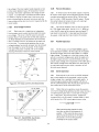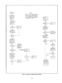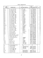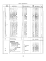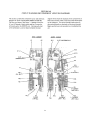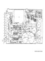
1
..----
DOCUMENT
,_-----..:!I~.......,
CONTROllE
DOCUMENT
MODULAR POWE_R SUPPLIES
MODELS 63005C AND 63315D
OPERATING AND SERVICE MANUAL FOR:
MODEL 63005C, SERIALS 1528A·00101 AND ABOVE
MODEL 63315D, SERIALS 1528A-00101 AND ABOVE
* For serials above 1528A·0010l
a change page may be included .
•
Don Rowe
Field Support Specialist
Fire Systems
T 519376 2430x417
8662982778 x417
F S19 372 1S81
[email protected]
www.gesecurity.com
625· 6th Street East
Owen Sound, ON N4K 5P8
Canada
WOltLOWIOf
....
.
Security
..... ~::. Agilent Technologies
Jim Nagy
Customer Service Representative
Test & Measurement
Agilent Technologies Canada Inc.
2250 bouL Anred Nobel
Saint-Laurent. Quebec
H4S 2C9
514 832 2836 telephone
514 832 2897 facsimile
lim [email protected]
wwwagilent.com
PAIlT~'fll
HP Part No. 5950-1738
Microfiche Part No. 5950-1752
Printed: August, 1975
SECTION I
GENERAL INFORMATION
1-1
1-6
DESCRIPTION
1-2
The two power supplies covered by this manual
employ switching regulation for high efficiency and compactness. Both models have a maximum output power of 110
watts. In the Model 63005C, this power is delivered by a
single 5V ±0.25V output with a 22-amp load capacity. The
Model 633150 also provides an adjustable 5V output and,
in addition, a pair of dual tracking outputs that can be set
within a ±11.4 to ±15. 75V range by a single screwdriver
adjustment. The Model 633150's three outputs have individual current restrictions of 18 amps, 2 amps, and 2 amps,
respectively, and within these limits can be operated at any
combination of currents that does not exceed the supply's
110W total output rating. (See Figure 3-5 for the load sharing
tradeoff for the Model 633150.)
1-3
Both models are SCR preregulated and use an advanced design 20kHz transistor switching regulator for
their 5V outputs. The ±11.4 to ±15.75V outputs of the
Model 633150 have two independent linear transistor series
regulators.
1-4
Adjustable foldback current limit circuits protect
all outputs against overload or short circuit damage by
limiting the outputs to between 65% and 130% of their
maximum ratings. Fixed overvoltage protection crowbar
circuits are activated at 6 to 7 volts on the 5V output and
at 16 to 18 volts on the ±11.4 to ±15. 75V outputs. They
reduce all outputs to less than 2 volts if anyone output
exceeds its trip voltage.
SPECIFICATIONS
1-7
Table 1-1 lists detailed specifications for these
power supplies.
1-8
Accessories
1-9
Accessories are available for mounting these supplies in a standard 19-inch equipment rack. Consult the
factory for information.
1-10
INSTRUMENT AND MANUAL
IDENTIFICATION
1-11
Hewlett-Packard power supplies are identified by
a two-part serial number. The first part is the serial number
prefix, a number-letter combination that denotes the date
of a significant design change and the country of manufacture. The first two digits indicate the year (10= 1970,
11 =1971, etc.), the second two digits indicate the week,
and the letter"A" designates the U.S.A. as the country
of manufacture. The second part is the power supply serial
number; a different sequential number is assigned to each
power supply, starting with 00101.
1-12
If the serial number on your instrument does not
agree with those on the title page of the manual, Change
Sheets supplied with the manual or Manual Backdating
Changes define the differences between your instrument
and the instrument described by this manual.
1-13
ORDERING ADDITIONAL MANUALS
1-14
One manual is shipped with each power supply.
Additional manuals may be purchased from your local
Hewlett-Packard field office (see list at rear of this manual
for addresses). Specify the model number, serial number
prefix, and Hp'Part number provided on the title page.
1·5
The 5V and ±11.4 to ±15. 75V outputs are isolated
from the chassis and from each other and may be grounded
to the ground terminal provided or floated at up to 42 volts
above ground.
Table 1-1. Specifications, Models 63005C and 633150
INPUT:
87/1 27Vac or 180-250Vac, single-phase, 48-63Hz.
VOltafle range field changeable on terminal block. Internally
fused at 5A.
AC INRUSH CURRENT:
Less than 20A peak at turnon.
~
, .....
LOAD EFFECT:
Less than 0.1 % for a load current change equal to the
current rating of the supply.
SOURCE EFFECT:
Less than .02% for any change within the specified
input voltage rating.
-.
1 ·1
Table 1-1. Specifications, Models 63005C and 633150 (Continued)
OUTPUT:
Model 63005C: 5V ±0.25V, 22A
Mode163315D: 5V iO.25V, 18A*
+11.4 to +15.75V, 2A*
-11.4 to 15.75V. 2A*
(Screwdriver voltage adjustments are accessible through
holes in the panel.)
*Maximum load currents cannot be obtained simultaneously.
See Figure 3·5 for load sharing tradeoff.
TRACKING ACCURACY (Model 63315D dual output):
±2%.
PARD (Ripple and Noise):
All outputs: Less than 5mV rms and 40mV Pop (20Hz
to 20MHz).
of maximum at 70°C ambient.
Storage: _55° C to +85° C.
COOLING:
Convection cooled. (In some applications, can be conduction cooled through surface at end of case after removing
finned heatsink. Consult factory for recommendations.)
THERMAL PROTECTION:
Heatsink-mounted thermostat shuts off output(s) if supply overheats due to high ambient temperature. Thermostat
automatically resets when unit cools to safe operating
temperature.
CURRENT LIMIT PROTECTION:
Accessible screwdriver adjustment(s) are factory set to
limit load current to approximately 120% (5V output) or
130% (± 12 to ±15V outputs) of rated max imum cu rrent.
Foldback current limit characteristics are shown in Figures
3-6 and 3-7. Adjustment range is approximately 65
to 130% of rated load current in Model 63005C and 65 to
150% in Model 63315D.
EMI CHARACTERISTICS:
Conducted EMI complies with VDE 0875/7.71,
Level N.
SAFETY STANDARDS:
Designed to conform to recommendations of IEC 348.
Approved by UL for inclusion in their Recognized Component Index under Guide OOFU2, File E51529.
DIELECTRIC WITHSTAND VOLTAGE:
Primary to case, 1500V rms for 1 minute.
Primary to output(s}, 1500V rms for 1 minute.
Output(s) to case, 500 Vdc for 1 minute.
OVERVOLTAGE PROTECTION:
Non-adjustable overvoltage crowbar reduces output(s)
to less than 2V when trip level of 6 to 7V is exceeded at
the 5V output or 16 to 18V is exceeded on either 12 to
15Voutput. In the Model 63315D, an overvoltage trip at
anyone output shuts down all three outputs.
INSULATION RESISTANCE:
At least 10 megohms from any output to case or from
5V output to ±12 to ± 15V outputs.
REVERSE VOLTAGE PROTECTION:
Output(s) are protected from damage due to the
application of a reverse polaritY:voltage.
LOAD TRANSIENT RECOVERY:
Less than 1.0msec (5V output) or 25psec (±12 to ±15V
outputs) for output recovery to within 1% of nominal out-
REMOTE SHUTDOWN:
A contact closure or TTL (low) input between the 5V
output's (-) or (- SEN) terminal and terminal E6 reduces
all supply outputs to zero volts. The outputs return to
normal on opening the contact or switching to a high
logic level.
put voltage following a load change from full to half load
or vice versa.
CARRYOVER TIME:
Output voltage remains within 2% of specified nominal
for more than 20msec while delivering full load current
following removal of ac input power.
TEMPERATURE COEFFICIENT:
Less than .015% output voltage change per degree
Celsius over the operating range from 0 to 40°C at constant
load and line voltage after 30 minutes warmup.
TEMPERATURE RANGES:
Operating: 0 to 40°C ambient. For temperatures greater
than 40°C, output current must be derated linearly to 50%
1-2
REMOTE SENSING:
Remote sensing terminals are provided which will correct
for a load lead ~oltage drop of up to 5% while maintaining
nominal voltage at the load. The load is protected if sensing
leads are inadvertently opened.
DIMENSIONS:
Refer to Figure 2-1 or 2-2.
WEIGHT (Net/Shipping):
Model 63005C: 3.2kg (7 Ibs)/4.1 kg (9 Ibs)
Model 63315D: 4.1kg (9Ibsl/5.0kg (11Ibs)
SECTION II
INSTALLATION
2-1
INITIAL INSPECTION
2-12
2-2
Before shipment, this instrument was inspected
and found to be free of mechanical and electrical defects.
As soon as the instrument is unpacked, inspect for any
damage that may have occurred in transit. Save?1I packing
materials until the inspection is completed. If damage if
found, a claim should be filed with the carrier immediately.
Also, a Hewlett-Packard Sales and Service office should be
notified.
2·3
Mounting Orientation
2-13
Figures 2-1 and 2-2 show outline and dimension
information. As shown in these figures, four mounting holes
are provided on the bottom of the supply and four more are
available at the rear if the heat sink is removed. If these sup·
plies are cooled by natural convection, the upright position
is the only orientation recommended. If they are cooled by
forced air or if the heatsink is removed and the supply is
mounted to a heat-conducting surface, they may be mounted
in any position.
Mechanical Check
2-14
2-4
This check should confirm that there are no broken
connectors and that the panel surfaces are free of dents and
scratches.
2·5
2-15
The Models 63005C and 633150 may be operated
from an 87 to 127Vac or a 180 to 250Vac, single-phase, 48
to 63Hz power source and can be adapted for either of these
input voltage ranges by the positioning of jumpers on termi·
nals E1 through E5 on TB 1. For 87 to 127V operation,
jumper El to E2 and E4 to E5. For 180 to 250V operation,
jumper E3 to E4 only. (When it is shipped, the supply's
input jumpers are connected for 87 to 127Vac operation.)
Both models draw a maximum input current of 4 amps. The
maximum input power is 190 watts for the Model 63005C
and 220 watts for the Model 633150.
Electrical Check
2-6
The instrument should be checked against its electrical specifications. Section V includes an "in-cabinet"
performance check to verify proper instrument operation.
2·7
Input Power Requirements
INSTALLATION DATA
2-8
The instrument is shipped ready for permanent
installation or bench operation. It is necessary only to
connect the instrument to a source of power and it is ready
for operation.
2·9
Location and Cooling
'.00
2-10
This instrument is air cooled. Sufficient space
should be allotted so that a free flow of cooling air can
reach the instrument when it is in operation. At least 1/2
inch clearance at the bottom of the unit is recommended to
permit proper air flow. The supply should be used in an
area where the ambient temperature does not exceed 40°C.
If operated at an ambient greater than 40° C, the supply's
output current must be linearly derated down to 50% at
70°C.
L--frlIO.JN1'fl«ifAST[J£R5
fi:'}2:1<lf'UCES:
I()l[ TH! f()JPf>:l.2 FASTENERS fY:POSf(J8't
REMOVAL
~
THE Hf ....1S1HiI.
Itf""r
fl(
US€O!N ¥CMlTI'iij T't1E $Uf'I'l.Y TO""
SU!TAlL[ HE IT -COHlJXTIHG SlJilfl.C[
!IlJT Tt+{l 00 NOT I'ROVI{)[ AD(OOArr
$TROCTUAL SUf>9'('AT TO niE SUPPl'
If USED lLON£
2·11
It is also possible to cool this supply through conduction by removing its finned heatsink and mounting the
rear surface of the supply to a suitable heat·conducting
surface. Consult the factory for specific recommendations.
Figure 2-1. Outline Diagram, Model 63005C
2-1
2-16
REPACKAGING FOR SHIPMENT
2-17
To insu re safe shipment of the instrument, n is
recommended that the package designed for the instrument
be used. The original packaging material is reusable. If it
is not available, contact your local Hewlett-Packard field
office to obtain the materials. This office will also furnish
the address of the nearest service office to which the instrument can be shipped and provide the Authorized Return
label necessary to expedite the handling of your instrument
return. Be sure to attach a tag to the instrument which
specifies the owner, model number, full serial number, and
service required, or a brief description of the trouble.
NOT( - THE: fCllJl 6·32 fAST[H[RS EJPOS£O
BY REIlIQV't. Of nt: t£A,TSlNK MAl'
IlE USED IN MOUNTING TlfE SUPflI..Y TO
A Sl/lTA8LE HEAT-CCHOUCTING
SORflC( auT no 00 NOT PFIJVlDE
A.OEQlIiTt STR'JCTURAl 'Sl/Pf'ORT 10
TIf£9JPP\.YIfUSEOlLM
Figure 2-2. Outline Diagram, Model 633150
2-2
SECTION III
OPERATING INSTRUCTIONS
3-1
RL to its maximum resistance and apply power to the supply. Decrease the resistance of RL gradually wh ile observing the output current indicated by the DVM. The
current should increase to some maximum value, which is
the current limit setting, and then begin to decrease. To
adjust the current limit setting, see paragraph 5-46.
g. (Model 633150 only). Check the operation of the
current limit circuit for the positive 11.4 to 15.75V Olltput by the method described in (f) above, but using a
variable load resistor with an adjustment range of about
4n to 15n and a 50W power rating. Repeat for the negative output. To adjust the current limit settings, see paragraph 5-46.
TURN-ON CHECKOUT PROCEDURE
3-2
The following checkout procedure serves as a brief
check that the supply is operational. This procedure or the
more detailed performance test of paragraph 5-6 should be
followed when the instrument is received and before it is
connected to any load equipment.
PREPARATION
a. Before connecting input power, check that jumpers
on terminals E1 through E50f TB1 are connected appropriately for the ac supply voltage to be used. (See paragraph
2-16.)
b. Connect all remote sensing terminals to the corresponding output terminals as shown in Figure 3-1.
c. Connect unit to input power source using AC, N, and
ground ( 4- ) terminals of TBt
OVERVOLTAGE PROTECTION CHECKS
h. Because the supply's output voltage adjustment ranges
are limited and the overvoltage trip circuits are not adjustable, checking the overvoltage trip circuits requires the use
of an external power supply. The supply needed for checking the overvoltage trip for the 5V output should be able to
supply 5 to 7 Vdc at a current of at least 2 amps. To avoid
causing damage to the supply under test, the external
supply's maximum available current should be no more than
5 amps. To check that the overvoltage trip circuit for the
5V output is operational, energize the external supply and
adjust its output to 7 volts. Energize the 63005C or
633150 supply and then momentarily connect the output
of the external supply across its 5V output terminals, negative to negative and positive to positive. After disconnecting
the external supply, check for the presence of voltage at the
outputs of the supply under test. All outputs should be at
zero volts. Oeenergize the supply under test for 10 seconds
and then restore power. Check that all outputs have returned to normal.
i. (Model 633150 only). A similar method is used for
checking the ±11.4 to ±15.75V outputs of the Model 633150.
An external supply is needed that can provide 15 to 18 Vdc
at a current of at least 0.5 amps. Its maximum available
current should be no more than 5 amps. To check the overvoltage trip circuit for the positive 11.4 to 15.75V output,
energize the external supply and adjust its output to 18
volts. Energize the 633150 supply and then momentarily
connect the output of the external supply across the (+) and
COMMON RETURN output terminals of the 633150, positive to positive. After disconnecting the external supply,
check that all outputs of the supply under test have dropped
to zero volts and that deenergizing the supply for 10 seconds
restores the outputs to normal.
VOLTAGE CHECKS
d. Check the voltage of the 5V output between terminals
(+) and (-) on TB2and,using a small screwdriver to turn the
VOLT AOJ control, set the output to the desired value within its 4.75 to 5.25V range.
e. (Model 633150 only). Check the voltages of the
positive and negative 11.4 to 15.75V outputs by measuring
from (+) to COMMON RETURN and from COMMON
RETURN to (-) on TB3. They should differ from each
other by no more than ±2%. Turn the VOLT AOJ control
to set these outputs to the desired voltage.
CURRENT LIMIT CHECKS
f. To check the operation of the current limit circuit
for the 5V output, connect the test setup shown in Figure
5-2 to the output, using a variable load resistor for R L
that can be adjusted from about 0.15n to about 0.5n.
The load resistor must be able to dissipate 110 watts. Set
TB2
TB3
+SEN
....----->IV') +
o
+
E6
Figure 3-1. Load Connections, local Sensing
3-1
j. (Model 633150 only). To check the overvoltage trip
circuit for the negative 11.4 to 15.75V output, repeat the
procedure given in step (i) above, except connect the external supply across the (-) and COMMON RETURN output
terminals of the 633150, negative to negative.
TB3
+I~~--...,
REMOTE SHUTDOWN
k. Verify that connecting a jumper between terminals
E6 and (- SEN) on TB2 reduces all outputs of the supply
to zero volts and that disconnecting the jumper restores all
outputs to their normal voltages.
Figure 3·2. Single Load, Local Sensing
3-3
If this brief checkout procedure or later use of
the supply reveals a possible malfunction, see Section Vof
this manual for detailed test, troubleshooting, and adjustment procedures.
3-9
To use the dual outputs to supply 22.8 to 31.5
volts to a single load, use the strapping arrangement shown
in Figure 3·2. Either the (+) or 1-) output terminal may be
grounded, as required. (See paragraph 3-12.)
3-4
3-10
Each load should be connected to the proper supply output terminals using separate pairs of connecting
wires. This will minimize mutual coupling effects between
loads and will retain full advantage of the low output
impedance of the supply. Each pair of connecting wires
should be as short as possible, should be of adequately
heavy gage, and should be twisted or shielded to reduce
noise pickup. If shield is used, connect one end to the power
supply ground terminal and leave the other end unconnected.
OPERATION
- - - CAUTION-Before applying power to the supply, make certain
that jumpers £1 through £5 on TB1 are connected
appropriately for the ac line voltage to be used.
3-5
The following paragraphs discuss the various operating modes and features of the Model 63005C and 633150
supplies. Their 5V outputs can be used with local or remote
voltage sensing. The :1;11.4 to ±15. 75V outputs of a Model
633150 supply can be used as a dual output supply ing positive and negative voltages or they can be connected to provide a single output providing 22.8 to 31.5 volts. Local or
remote sensing can be used with both the dual and single load
connections. The 5V outputs of two single output supplies
can be connected in parallel and two or more of them can be
connected in series.
3-11
If load considerations require that the output power
distribution terminals be remotely located from the power
supply, then the power supply output terminals should be
connected to the remote distribution terminals by a pair
of twisted or shielded wires and each load separately connected to the remote distribution terminals. Remote
sensing should be used under t~ese circumstances. (See
paragraph 3-14.)
3-12
3-6
The DC Power Supply Handbook, Application
Note 90A, contains a considerable amount of general
information on using regulated dc power supplies effectively
and is available at no charge from your local HP sales office.
3-7
Grounding
3-13
The 5V output can be used either as a positive or
a negative supply by grounding one of its output terminals
or one end of the load.
IWARNING I
Connecting loads
3-8
Figure 3-1 shows the strapping arrangement for
connecting loads to the supply using local voltage sensing
and supplying two separate loads from the ±11.4 to ±15. 75V
outputs. The positive (master) supply powers RL2 and the
negative (slave) supply powers R L3 . As the VOLT AOJ
control for the dual outputs is adjusted, the slave supply's
output tracks that of the master within ±2%. Either terminal of the 5V output and anyone terminal of the dual output may be grounded, if desired, either at the supply's ground
(~) terminal or at the load. (See paragraph 3-12.)
3-2
Ground at only one point in the setup and always
use two wires to connect the load to the supply.
This eliminates the possibility of load current
return paths through the ac ground line which
could open the chassis ground path and create
a hazardous condition.
This supply can also be operated at up to 42 Vdc above
ground, if neither output bus is grounded.
3-14
Remote Sensing
3-15
Remote sensing is used to maintain good regulation
at the load by reducing the degradation in regulation that
would occur due to the voltage drop in the leads between
the power supply and the load. For reasonable load lead
lengths, remote sensing greatly improves the performance
of the supply. However, if the load is located a considerable distance from the supply, added precautions must be
observed to obtain satisfactory operation. Because the
voltage drop in the load leads subtracts directly from the
available output voltage, it is recommended that the total
drop in both load leads not exceed 5% of the supply's nominal output voltage.
3-16
The leads from the sensing terminals to the load
carry much less current than the load leads, so these leads
need not be as heavy as the load leads. However, they
must be twisted or shielded to minimize noise pickup.
3·19
Output Ratings
3-20
Model 63005C. The Model 63005C is capable of
providing 22 amps at 5V ±0.25V at ambient temperatures
up to 40°C. Above 40°C, the output current must be
linearly derated to 50% at the maximum operating temperature of 70°C.
3-21
Model 63315D. Individually, the maximum output
currents of the Model 633150 are 18 amps at the 5V
±0.25V output and 2 amps at each of the 11.4 to 15.75V
outputs. These maximum currents are not available
simultaneously, though, due to the 110W total output
rating of the supply. Figure 3-5 illustrates the load sharing
tradeoff between the 5V and the ± 11.4 to ± 15. 75V outputs.
Above 40°C, these output currents must be linearly derated
to 50% at the maximum operating temperature of 70°C.
20
TB2
r---k".,;li +SEN
+SEN
+
COM
\----+0"11- SEN
o
:;::;
-:::
5VOUTPUT
LOAD CURRENT
~
I
I
10
---r-------
5
SEN
- SEN
I
I
)
E6
I
15
\
;:::
RET
RET
5V AT ISA MAX
IS~
TB3
I
I
±15V
AT
2A MAX
:
o L.-~I-:"13::3-2l-----'3--4'--------:-5
/
1.11.4 TO 1.15.75V(mTAL) OUTPUT CURRENT
Figure 3·3. Load Connections, Remote Sensing
Figure 3-5. Load Sharing Tradeoff, Model 63315D
3·22
3-17
Figure 3-3 shows the strapping arrangement for
connecting loads to the supply using remote sensing. When
the loads on the dual outputs of a Model 633150 are located a considerable distance from each other, the COMMON
RETURN load lead and the RETURN SENSE lead should
be connected together at a remote sensing point that is
equidistant from the two loads. This ensures that the
regulation characteristics of both outputs will be equal.
Current Limiting
3-23
The current limiting characteristics of these supplies
are shown in Figures 3-6 and 3-7. The current limit circuits
in these supplies provide fold back limiting, which reduces
the output current as the voltage decreases. This results
in a short-circuit current that is less than the maximum
available at the rated output voltage. The circuits are selfrestoring and return the output voltage to normal when
the overload is removed. Figures 3-6 and 3-7 show
the approximate factory settings and adjustment ranges for
the current limiting circuits. Changing the setting of the
control affects the maximum output current as shown but
has no effect on the short circuit current. Procedures for
adjusting the operating points of the current limit circuits
are given in paragraph 5-46.
3-18
Figure 3-4 shows the connections necessary for
powering a single load from the dual output using remote
sensing. The (+ SEN) and (- SEN) sensing leads should be
connected as close as possible to the load.
+ IClI+----4
COM
RET
RET
SEN
3-24
When adjusting the current limit, ensure that the
new set point is at least 20% above the expected operating
current. Operating the supply too close to the current
limit set point may degrade performance.
Figure 3-4. Single Load, Remote Sensing
3-25
3-3
Since, in the dual outputs of the Model 633150,
3-28
the voltage of the slave (negative) supply depends on that
of the master (positive) supply, the occurance of current
limiting in the master supply reduces the voltage of both
outputs. If a single load is connected across both outputs
as shown in Figures 3-2 and 3-4, the initial current limit
point is determined by the current limit circuit with the
lower setting and the short circuit current is governed by the
master supply.
3-26
3-29
If remote control of the power supply is required,
all outputs of the supply can be operated remotely through
a contact connected from terminal E6 on TB2 to either
the (-) or the (- SEN) terminal of the 5V output. Closing
this contact reduces all outputs to zero volts; opening it
restores all output voltages to normal.
Overvoltage Protection
3-30
The remote shutdown input can also be controlled
by a TTL digital input signal. Use the (-) or (- SEN) terminal of the 5V output as the common input and apply TTL
logic levels to terminal E6. A low logic level shuts down
the supply; a high logic level input resotres the outputs.
3-27
Each output of this supply has an independent
fixed crowbar circuit to protect sensitive loads from excessive voltages. The circuit for the 5V output is activated
between 6 and 7 volts and the ones for the dual outputs of
the Model 63315D are activated between 16 and 18 volts.
After a crowbar circuit fires, all outputs of the supply fall
to zero volts. To restore normal operation after an overvoltage shutdown has occurred, ac power must be removed
from the supply for at least 10 seconds. If the crowbar
trips again when power is restored, refer to the troubleshooting information in Section V of this manual.
3-31
145A
285A
--7
/
I
I
4V
I
3V
EOUT
I
2V
/
/
/~
FACTORY
/
SETTING
3-33
I /
I /'
IV
Parallel Operation
3-32
The 5V outputs of two Model 63005C supplies
can be operated in parallel. Set the output of one supply to
the desired voltage, and set the other supply for a slightly
higher voltage. The supply set to the lower output voltage
will act as a constant voltage source, while the supply set to
the higher output will act as a current-limited source, dropping its output voltage until it equals that of the other supply
The constant voltage source will deliver only that fraction of
its total rated output current which is necessary to fulfill
the total current demand.
RATED OUTPUT
CURRENT
(18A OR 22Al
5V
Remote Shutdown
Series Operation
I
o l.-_'_----4.~_'___'__....J-_'_
I lOA
3-34
Either the 5V or the ±11.4 to ±15. 75V outputs of
two or more supplies can be cOf\nected in series to obtain
a higher voltagp. than i~ available from a single supply. The
restriction against operating these supplies with their outputs at a potential greater than 42 volts above ground limits
the number which can be connected in series.
30A
20A
8A
(TYPICAL)
JOUT
Figure 3-6. 5V Output, Current Limit Characteristics
MIN. ADJ. RANGE
3-35
Notice that series operation creates the possibility
of a reverse voltage being applied across the output terminals
of a deenergized supply that is in series with an energized
one. If this occurs, the resulting reverse current flows
through A2U4 in the 5V supply or diodes A3CR 1 or CR 16,
which protecnhe ±15V outputs against reverse voltage.
I
±114 TO
± 15. 75Vr------,.;;;;;;;..-----:;;;...--=7
FACTORY
SETTINGS:
MASTER
--+L--...
SLAVE
/ I
(SEPARATELY ! I
ADJUSTA8l£)! I
EOUT
!
o
/ I
I
---CAUTION---
t
2A
When operating these supplies in series,
turn them on and off simultaneously if
possible. If this cannot be done, ensure
that all units are turned on or off within
25 seconds to minimize the possibility
of damage to the output diodes.
3A
04A 07A
(TVPICALJ
lOUT
Figure 3-7. Model 63315D, Dual Output,
Current Limit Characteristics
3-4
SECTION IV
PRINCIPLES OF OPERATION
4-1
INTRODUCTION
100 volts dc. The preregulator control circuit consists of
a comparator-amplifier which compares the voltage at its
input to a zener reference voltage and controls the firing
delay of a programmable unijunction transistor in the
firing circuit. During each half-cycle of the ac line input,
one output pulse from the unijunction is coupled to the
SCR gates by pulse transformer A1Tl. If the 100V output tends to increase, the comparator-amplifier reduces the
conduction angle of the SCRs. If the voltage tends to
decrease., the conduction angle is increased. The reset
switch discharges the timing capacitor in the firing circuit
at the end of each half-cycle of the ac line input.
4-2
This section presents the principles of operation
for the rvlodels 63005C and 633150 switching-regulated
modular power supplies. The Model 63005C single-output
supply employs just two of the circuit boards shown in the
simplified schematic of Figure 4-1, Al and A2.' The Al
board contains an SCR preregulator whose dc output is
filtered to provide a regulated 100V dc input to a singletransistor switching regulator. On the A2 board, the 20kHz
output from a switching regulator transformer secondary
is rectified and filtered to produce a regulated 5V dc output
at a maximum current of 22 amps. Also on the A2 board
are the voltage control, output current limit, and overvoltage protection circuits for the 5V output.
4-8
The supply is designed for two ac Iine voltage
ranges (87 to 127Vac and 180 to 250Vac) and can easily
be converted from one to the other by changing jumper
positions on terminals El through E5 on an external
terminal block.
4-3
In the Model 633150, Aland A2 boards very
similar to those in the Model 63005C produce a 5V output
with a maximum current rating of 18 amps, and an additional A3 board contains a dual linear regulator which produces
two tracking outputs with an output voltage range of ±11.4
to ±15.75 volts at a maximum current of 2 amps. The maximum load currents for the ±15V (nominal) outputs and the
5V output cannot be obtained simultaneously but are interdependent as shown in Figure 3-5. The ±15V outputs draw
power from two additional secondaries on the 20kHz switching regulator transformer and are regulated by two seriestransistor regulators connected in a master-slave configuration. These outputs are individually protected against overcurrent and overvoltage. An overvoltage condition at any
one of the supply's three outputs shuts down all three
outputs.
4-4
4-9
20kHz Switching Regulator. The supply's 5V
output is regulated by a single-transistor switching regulator
connected in series with the 100V output of the pre regulator and the primary winding of power transformer A2T2,
on the A2 board. The 5V output is regulated by controlling
the percentage of the time that switching transistor A105
conducts. The transistor's switching rate is controlled by
an IC timer in the 20kHz clock circuit. The on-time of
the switching transistor is controlled by a pulse width
modulator located on the A2 board.
4-10
The clock establ ishes the basic tim ing cycle for
the regulator by generating an alternating sequence of
switching transistor turn-on and turn-off pulses which are
conducted to the base of A105 through pulse transformer
A1T2. The maximum duty cycle of the switching transistor
is 60%. Each time that a turn-on clock pulse switches
A105 on, a base drive pulse produced by a regenerative
bias winding of A2T2 keeps A105 on until a turn-off signal
appears.
SIMPLIFIED SCHEMATIC DIAGRAM
DISCUSSION
4-5
The following discussion of the overall circuit
operation of the Models 63005C and 633150 is based on
the simplified schematic of Figure 4-1.
4-6
AC-DC Converter Assembly (A1 Board)
4-11
Following each clock turn-on pulse, there are three
signals that can turn off the switching transistor. They are:
1. a voltage control pulse from the pulse width
modulator,
2. a primary peak current limit pulse from a current
limit comparator in the switching regulator,
3. a turn-off pulse from the clock.
The first of these three signals to appear after each clock
4-7
Preregulator. The ac input to the A1 board is
connected through an RFI filter directly to the input of
a preregulator bridge composed of two diodes and two
SCRs. The firing angle of the SCRs is controlled by the
preregulator control circuit so that their full-wave rectified
output, after being filtered by a 2-section LC filter, averages
4-1
turn-on pulse turns A105 off until the next clock turn-on
pulse initiates the next operating cycle.
4-12
Normally, it is the voltage control pulse that turns
off A105. An optically coupled isolator in its signal path
provides electrical isolation between primary and secondary
circuits. The timing of this pulse controls the voltage of
the 5V output. A tendency for the output voltage to decrease is compensated by an increase in the delay between
the clock turn-on pulse and the subsequent turn-off pulse
from the pulse width modulator. If the output tends to
increase, the delay is reduced. Slow turn-on control, output
current limit, and remote shutdown signals are also communicated through this path from the A2 board. The generation
of these signals is covered in the discussion of the A2 board.
4-13
The second switching transistor turn-off signal
listed in paragraph 4-11 is produced by a fixed current
limit comparator that monitors the peak current through
A1 R37 du ring each pulse that A105 conducts and imme- .
diately turns off A105 if this current exceeds a preset
level. This current limit circuit on the primary side of the
~oc
COHV£RTER
ASSE.",.,,,,LY'---a~:E
transformer serves as a backup to the protection provided
by an adjustable output current limit circuit on the secondary side. The primary peak current limit circuit has a higher
set point than the one on the secondary side and functions
solely to protect the switching transistor.
4-14
The third turn-off signal listed in paragraph 4-11,
the clock turn-off pulse, limits the maximum on-time of
A105 to 30 microseconds of each 50psec operating cycle
to avoid transformer saturation.
4-15
Between the time a turn-off signal ends A105's
conduction interval and the time the clock turn-on pulse
turns A105 on again, the collapsing field of transformer
A2T2 generates a current pulse in a flyback winding which
CR 18 conducts to return th is energy to capacitor A1C13 at
the input to the switching regulator. This keeps the transformer core out of saturation by resetting it before the
next operating cycle begins.
4-16
The clock receives its +14.7V operating bias from
a shunt zener regulator composed of R21 and VR2. An
------,
_
,I
5V1025'l,.!, +
I
-,
I
I
I
I
~J:=====~W-==-/&",~,I~t}
l.?OtHI
I SWITCHI1(6
R21
L5fJi t!Y.'-0fJ..
_
+14TV
I
l!!!~[!!!Lg~
c;2'H!2L
:
~
r-
r-''''--+-+--i<l! lEG
I"
<
YO,
,
I
Iii
,
I
L
_
,1
!I
:I
;
:r
U L_'-__--~-.J...--~~·
J
crIwnl
Figure 4·1. Models 63005C and 633150 Simplified Schematic Diagram
4-2
excessive A105 switching transistor heatsink temperature
opens thermal switch 51 to interrupt the 1OOV supply to
the clock bias regulator. This stops the clock to leave
A105 safely turned off. 51 remains open until the heatsink has cooled to a safe operating temperature_
parator. The input pulse to the isolator turns on a light
emitting diode (LED) which turns on a phototransistor.
When the phototransistor conducts, it turns off switching
transistor A105.
4-22
Now that A105 has been turned off, the negativegoing voltage at the input to inductor A2L 1 resets the pulse
width modulator for the next operating cycle, which begins
when the clock turns on A105 again.
4-17
In case of an overvoltage condition at the 5V
output of the Model 63005C or at any of the outputs of
the triple output model, an overvoltage trip pulse fires an
5CR connected as a clock shutdown switch which shorts
the 14.7V bias supply to the clock to shut down the
switching regulator.
4-18
5V Switching Regulator Assembly
(A2 Board)
4·19
On the A2 board, the 20kHz ac voltage at one
secondary of switching regulator power transformer A2T2
is half-wave rectified and then filtered by a 2-section LC
filter to provide a regulated 5V dc output. This board also
contains circuits that regulate the output voltage, turn on
the switching regulator slowly when power is first applied,
limit the output current, and shut down the supply if an
overvoltage occurs at the 5V output. The output voltage
regulation, slow turn-on, and output current limit functions
are controlled through input signals to the pulse width
modulator, whose output is transmitted through the
optically coupled isolator on the A1 board to the switching
transistor.
4·20
Voltage Regulation. Each output pulse from the
pulse width modulator causes switching transistor A105
in the switching regulator to stop conducting_ Thus, the
output voltage is regulated by controlling the duration of
OS's conduction intervals. The pulse width modulator
controls the timing of its output pulses by comparing two
input signals. One of them is a dc level received from the
output of the constant voltage comparator. This signal
varies depending on the difference between the supply's
output voltage and that of a fixed reference. An increase
in the supply's output voltage changes this dc level in the
negative direction. The pulse width modulator compares
this dc level to a combined dc and ripple signal taken
from the output of the first section of the LC filter.
4-21
When the clock on the A1 board turns A105 on,
the positive voltage at the secondary of transformer A2T2
begins charging A2C5 through inductor A2L 1. The positive-going ramp voltage waveform on these capacitors and
the dc level from the constant voltage comparator are
both attenuated and appl ied to two inputs of a comparator
within the pulse width modulator_ The pulse width
modulator's output pulse to the isolator is produced
each time the dc plus ripple voltage input from A2C5
exceeds the dc level input from the constant voltage com-
If the voltage at the 5V output tends to decrease,
4-23
the dc level input to the pulse widthmodulator increases.
As a result, it takes slightly longer for the ramp waveform
of the ripple voltage to exceed this higher dc level at the
comparator inputs. Thus, the delay before A105 is turned
off is increased slightly to increase A105's conduction time
and compensate for the decreased output.
4-24
Slow Turn-on Control. The slow turn-on control
circuit prevents an output voltage overshoot from occuring
and actuating the overvoltage trip circuit when ac power is
first applied to the supply. The circuit consists of an roc
network that slows down the initial rise in voltage of the
dc level input to the pulse width modulator from the constant voltage comparator. This causes the switching
regulator to bring up the output voltage smoothly to its
nominal value.
Output Current Limiting. The 5V output is pro4-25
tected against an overlo'ad or short circuit by an adjustable
foldback current limit circuit which reduces the output
voltage and current as an overload increases. The current
limit characteristics of the SV output are shown in Figure
3-6 or 3-7. To obtain these current limit characteristics,
the output current limit comparator compares the voltage
developed across current sampling resistor R24 to a
reference voltage developed across R20. When the voltage
across R24 exceeds this reference, the output of the comparator reduces the dc level input to the pulse width
modulator to reduce the supply's output. The resulting
reduction in output voltage decreases the contribution made
to the reference voltage across R20 by current from the
positive output line through R34 and R18. This reduces
the output current limiting point as the output voltage
decreases. If the output is short-circuited, the circuit
reduces the output current to the value determined by the
reference voltage developed by the current through R17
alone. For this reason, output current limit adjust R34
affects the maximum output current while leaving the
short-circuit current fixed.
4-26
Remote Shutdown. A contact closure or TTL input signal applied between remote shutdown terminal E6
and either the negative output or the negative sensing
terminal of the 5V supply reduces all outputs of the supply
4-3
to zero. This input signal shuts down the outputs by lowering the dc level input to the pulse width modulator. The
outputs of the supply return to normal on removal of the
remote shutdown input signal.
4-27
Overvoltage Protection. An overvoltage protection
circuit monitors the 5V output and fires SCR A201 if the
voltage exceeds a preset trip level of 6 to 7 volts. When
A201 fires, it immediately discharges the filter capacitors
across the 5V output to reduce the output to less than 2
volts. At the same time, a current pulse from A2T1 fires
the clock shutdown switch SCR on the A1 board to remove
power from the clock and shut off A105. This reduces all
output voltages to zero. In order to restore the supply to
operation, its ac input must be removed for a minimum of
10 seconds and then reappl ied.
4-28
Dual Linear Regulator Assembly
(A3 Board) (Model 633150 only)
4-29
Two series-transistor regulators on the A3 board
provide dual tracking outputs of ±11.4 to ±15.75 volts.
The input power to these regulators is obtained from two
additional secondary windings of transformer A2T2 and
is half-wave rectified and filtered on the A3 board.
4-30
Voltage Regulation. The regulators for the positive
and negative outputs are similar except that the one for
the positive output compares its output voltage to that of
a zener reference while the one for the negative output
compares the voltage at the COMMON RETURN output
terminal to the voltage at the junction of two equal resistors,
A3R27 and A3R28, which are connected across the posi-
4-4
tive and negative outputs. This is why the output voltage
of the negative (or slave) supply matches that of the positive (or master) supply within a ±2% tolerance and a single
voltage adjustment control, A3R 11, controls both outputs.
The constant voltage comparators regulate the outputs of
the supply by controlling the conductance of series regulator transistors A301 and A304.
4-31
Output Current Limiting. A current limit comparator for each regulator monitors the voltage drop
across current sampling resistor R7 or R22 and compares
it to an adjustable reference voltage across R9 or R23 that
is derived from the regulator's output. If the voltage drop
across the current sampling resistor exceeds the reference
voltage, the comparator's output signal to the series regulator causes the output voltage and current to be reduced.
This reduction in the output voltage reduces the current
limit circuit's reference voltage to produce the foldback
current limit characteristic shown in Figure 3-8. Because
of the dual tracking interconnection between the positive
and negative suppl ies, the output voltages of both are
reduced if the positive output is overloaded.
4-32
Overvoltage Protection. To protect loads on the
±15V outputs against overvoltage, an overvoltage protection
comparator monitors each output and fires an SCR connected across the ±15V outputs if either exceeds the preset
trip level of 16 to 18 volts. When SCR A306 fires, it shorts
the ±15V outputs and simultaneously sends an overvoltage
trip pulse through A2T1 to the clock shutdown switch on
the A1 board to shut down the clock. Thus an overvoltage
condition at any of the triple output supply's three outputs
will shut down the entire supply.
SECTION V
MAINTENANCE
5-1
INTRODUCTION
5-5
Table 5-1 lists the test equipment required to perform the various procedures described in this section.
5-2
Upon receipt of the power supply, the performance
test of paragraph 5-6 can be made. This test is suitable for
incoming inspection. Section III contains a quick but less
comprehensive checkout procedure which can' be used in
lieu of the performance test if desired.
5-3
If a fault is detected in the power supply while
making the performance test or during normal operation,
proceed to the troubleshooting procedure in paragraph
5-27. After troubleshooting and repair, repeat the performance test to ensure that the fault has been properly corrected and that no other faults exist. Before performing
any maintenance check, turn on the power supply and
allow a half-hour warm-up.
5-4
5-6
PERFORMANCE TEST
5-7
The following test can be used as an incoming
inspection check and appropriate portions of the test can
be repeated to check the operation of the instrument after
repairs. The tests are performed using the specified nominal
input voltage for the unit. If the correct result is not
obtained for a particular check, proceed to troubleshooting
(paragraph 6·27).
- - CAUTION-Before applying power to the supply, make
certain that jumpers E 1 through E5 on TB1
are connected appropriately for the ac line
voltage to be used.
TEST EQUIPMENT REQUIRED
Table 5-1. Test Equipment Required
TYPE
REQUIRED
CHARACTERISTICS
USE
RECOMMENDED
MODEl
Digital
Voltmeter
Sensitivity: 100,uV full scale
(min.). Input impedance:
10 megohms (min.).
Measure DC voltages:
cal ibration procedures
Variable
Voltage
Transformer
Range: 90-130Vac
Equipped with voltmeter
accurate within 1 volt
Vary AC input
-----
Oscilloscope
Sensitivity: 5mV/cm.
Bandwidth: 20MHz (min.)
Differential input
Display transient response and ripple and
noise waveforms.
HP 180A with 1821A,
and 1801A or 1803A
plug·ins.
Repetitive
Load Sw.
Rate: 60Hz, 2,usec
rise and fall time
Measure transient
response.
See Figure 5-4
Resistive
Loads
Tolerance: ±5%
Power supply load
resistor (fixed resistor
or rheostat).
James G. Biddl~
("Lubri-Tact"
Rheostat)
Current
Sampling
Resistor (Shunt)
Accuracy: 1%
Measure 5V output
current; Measure ± 15V
output current
Empro Shunt, A-50-50;
0.1 n resistor HP No.
0811-2061
.
5-1
HP 3450A
5-8
General Measurement Techniques
DIGITAL
VOLTMETER
POWER SUPPLY
UNDER TEST
5-9
Connecting Measuring Devices. To achieve valid
results when measuring the load effect, PARD (ripple and
noise), and transient recovery time of the supply, measuring
devices must be connected across the supply's sensing terminals. If a measurement were made across the load, it
would include the impedance of the leads to the load.
This impedance can easily be several orders of magnitude
greater than the supply impedance, and would thus invalidate fhe measurement. To avoid mutual coupling effects,
each measuring device must be connected directly to the
supply's sensing terminals by separate pairs of wires.
SEN -
+
+
SEN
C>+--------i--q
I
I
I
_J
CURRENT
SAMPLING
RESISTOR
(SHUNT)
-
GU
I
I
I
I
I
I
I
I
I
I
____ JI
5-10
Output Current Measurements. Accurate output
current measurements can be made by inserting a low resistance current sampling resistor in series with a load resistor
of appropriate resistance and wattage. Table 5-1 recom·
mendes two four-terminal resistors suitable for use as
current sampling resistors for the 5V and ± 15V outputs.
Figure 5-1 shows a four-terminal meter shunt. The load
current through a shunt must be fed to the extremes of the
wire leading to the resistor while the sampling connections
are made as close as possible to the resistance portion itself.
Figure 5-2. Rated Output, Test Setup
c. Apply input power to the supply and, with the load
switch open, set the voltage of the 5V output to any desired
value within the adjustment range. This output voltage can
be used for all remaining 5V performance tests.
d. Connect the voltmeter across the current sampling
terminals of the current sampling resistor, close the load
switch, and adjust RL until the voltmeter indicates a voltage
drop corresponding to the 5V output's maximum rated
current.
e. Reconnect the voltmeter across the (+ SEN) and
(- SEN) terminals of the 5V output and recheck its output
voltage. It should be within 0.1 % of the value set in step (c).
f. Steps (f) and (g) apply only to the Model 633150.
Use the same procedure described in steps (a) through (e)
above to check the +11.4 to +15. 75V output. Connect a
switch, a load resistor of appropriate value, and a current
sampling resistor in series between the (+) and the COMMON
RETURN terminals and monitor the output voltage across
the (+ SEN) and RETURN SENSE terminals.
g. Check the -11.4 to -15.75V output by using the
procedure described in steps (a) through (e) above. Load
the COMMON RETURN and (-) terminals and monitor
the output voltage across the RETURN SENSE and (- SEN)
terminals. Do not readjust the output voltage; the voltage
of the negative supply should be within 2% of the positive
supply's voltage.
NOTE
Output current limiting would interfere with
accurate measurements of the supply's performance. Avoid current limiting by making
certain that the current limit adjustments are
set sufficiently above the rated output current.
5-11
+
Rated Output
5-12
To check that the supply will furnish its rated output voltage(s) and current(s), proceed as follows:
a. Connect in series across the (+) and (-) terminals
of the 5V output a suitable load resistor, a current sampling
resistor, and a switch, as shown in Figure 5-2. The load
resistor must be of the proper value and of adequate wattage
to draw full rated current from the 5V output.
b. Connect a digital voltmeter across the (+ SEN) and
(- SEN) terminals of the 5V output, observing correct
polarity.
5·13
Load Effect (Load Regulation)
Definition: The change LlE OUT in the static
value of dc output voltage resulting from a change in load
resistance from open circuit to a value which yields maximum rated output current (or vice versa).
CURRENT SAMPLING
TERMINALS
TO UNGROUNOED
TO GROUNDED
TE R M I No'lL OF .-JV)I,'I\r---c~wro-----t.. TE RMIN AL OF
POWER SUPPLY
POWER SUPPLY
To test the load effect:
a. Connect a full load resistance and a digital voltmeter
across the (+) and (-) terminals of the 5V output, as shown
in Figure 5-2.
b. Turn on the supply and record the voltage across
5-14
Figure 5-1. Current Sampling Resistor Connections
5-2
the 5V output's sensing terminals.
c. Disconnect the load resistor and recheck the DVM
indication. It should be within 0.1% of the reading in step
(c).
POWER SUPPLY CASE
d. Repeat steps (a) through (c) for each of the remain·
ing supply outputs.
OSCILLOSCOPE CASE
AC--t-____
"'---+-rJ- AC
ACC
GND
ACC
GND
5-15
I
I
Source Effect (Line Regulation)
Definition: The change D. EOUT ' in the static
value of dc output voltage resulting from a change in ac
input voltage over the specified range from low line to high
line or from high line to low line.
I
I
I
G
To test the source effect:
a. Connect a variable autotransformer between the
input power source and the power supply ac input.
b. Connect a full load resistance and a digital voltmeter across the 5V output of the supply.
c. Adjust the autotransformer for a low line input.
d. Turn on the power and record the DVM indication.
e. Adjust the autotransformer for a high line input
and recheck the DVM indication. It should be within .02%
of the reading in step (d).
f. Repeat steps (b) th;ough (e) for each of the
remaining supply outputs.
G
EG
VERTICAL
INPUT
~--_ ......
--&-_~=-=---
L
5-16
5-17
I
I
I
I
J
A. INCORRECT METHOD - GROUND CURRENT lG PRODUCES 60
CYCLE DROP IN NEGATIVE LEAD WHICH ADDS TO THE POWER
SUPPLY RIPPLE DISPLAYED ON SCOPE.
POWER SUPPLY CASE
OSC I LLOSCOPE CASE
AC--t-____
,..---+..,rl- K;
ACC
GND
ACC
GND
+
VERTICAL
INPUT
G
G
B. A CORRH:T METHOOE USING' A SINGLE ENDED SCOPE. OUTPUT
FLOATED TO BREAK GROUND CURRENT LOOP, TWISTED PAIR
REDUCES STRAY PICKUP ON SCOPE LEADS.
PARD (Ripple and Noise)
Definition: The residual ac voltage which is superimposed on the dc output of a regulated power supply.
Ripple and noise may be specified and measured in terms
of its rms or peak-to-peak value.
Figure 5-3. Ripple and Noise, Test Setup
potential difference exists between the supply and the
oscilloscope, it is recommended that they both be plugged
into the same ac power bus. If the same bus cannot be
used, both ac grounds must be at earth ground potential.
5·18
Measurement Techniques. Figure 5-3A shows an
incorrect method of measuring POp ripple. Note that a
continuous ground loop exists from the third wire of the
input power cord of the supply to the third wire of the
input power cord of the oscilloscope via the grounded
power supply case, the wire between the negative output
terminal of the power supply and the vertical input of the
scope, and the grounded scope case. Any ground current
circulating in this loop as a result of the difference in
potential EG between the two ground points causes an
IR drop which is in series with the scope input. This I R
drop, normally having a 60Hz line frequency fundamental,
plus any pickup on the unshielded leads interconnecting
the power supply and scope, appears on the face of the
CRT. The magnitude of this resulting signal can easily be
much greater than the true ripple developed between the
plus and minus output terminals of the power supply and
can completely invalidate the measurement.
5-20
To verify that the oscilloscope is not displaying
.ripple that is induced in the leads or picked up from the
grounds, the (+) scope lead should be shorted to the (-)
scope lead at the power supply terminals. The ripple value
obtained when the leads are shorted should be subtracted
from the actual ripple measurement.
5-21
Measurement Procedure. To measure the ripple
and noise on each supply outputs, follow the steps below.
If a high frequency noise measurement is desired, an
oscilloscope with sufficient bandwidth (20MHz) must be
used. Ripple and noise measurements can be made at any
input ac line voltage combined with any dc output voltage
and load current within rating.
a. Connect an oscilloscope or rms voltmeter across
an output of the supply as shown in Figure 5·38.
b. Energize the supply and observe the oscilloscope
or meter indication. The ripple and noise should not be
5-19
Figure 5-38 shows a correct method of measuring
the output ripple of a constant voltage power supply using
a single-ended scope. The ground loop path is broken by
floating the power supply output. To ensure that no
5-3
c. Adjust the oscilloscope to display the loading and
the unloading transients produced by the operation of the
load switch. Recovery to within 1% of the nominal output
voltage should occur within 25 microseconds as shown in
Figure 5-5.
greater than 5mV rms or 40mV peak-to-peak.
c. Repeat for the remaining supply outputs.
5-22
Load Transient Recovery Time
Definition: The time it takes for the output voltage
to recover to within 1% of the nominal output following a
step change in output current from full to half load or vice
versa.
5-25
5-Volt Output. The mercury-wetted relays recom·
mended for use in the repetitive load switch described in
Figure 5-4 have a maximum current limitation of 5 amps.
For this reason, some other type of repetitive load switch
with a higher current capacity is required for testing the load
transient recovery time of the 5V output. The use of a solid
state electrical load with pulse modulation capabilities such
as the Transistor Devices Dynaload DlP 50-60-1000 is one
way to avoid the rise time and switching noise limitations
of mechanical switches at currents above 5 amps.
±11.4 to ±15.75-Volt Outputs. To test the load
5-23
transient recovery time, a r~petitive load switch with a fast
switching time is required for loading and unloading the
supply. Figure 5-4 shows one way of constructing one
using a relay with mercury-wetted contacts. When this load
switch is connected to a 60Hz ac input, the mercury relay
opens and closes 60 times per second. The 25kSl control
adjusts the duty cycle of the load current switching to reduce jitter in the oscilloscope display. This load switch can
also be used with a 50Hz ac input.
5·26
To check the load transient recovery time of the
5V output, proceed as follows:
a. Connect test setup as shown in Figure 5-4, but in
place of the load switch and contact protection network
shown, substitute a solid state repetitive load switch with
a current capacity of at least half of the supply's rated output and a rise time of less than 100 microseconds. (Since
the supply's recovery time is specified for a change between
half and full load, the switch conducts only hal f of the
supply's rated output.) Each load resistor (R ) is twice the
T
normal full load resistance.
b. Turn on the supply and the load switch.
c. Adjust the oscilloscope to display the loading and
the unloading transients produced by the operation of the
load switch. Recovery to within 1% of the nominal output
voltage should occur within 1 millisecond as shown in
Figure 5-5.
5·24
To check the load transient recovery time of each
of the ±11.4 to ±15. 75V outputs of the Model 633150,
proceed as follows:
a. Connect test setup as shown in Figure 5·4. Each
load resistor (R T ) is twice the normal full load resistance.
b. Turn on the supply and close the line switch on the
repetitive load switch.
POWER SUPPLY
UNDER TEST
OSCILLOSCOPE
1-
+
G
RT
RT
(NOTE 4)
CONTACT PROTECTION
NETWORK
r - (NOTE 3) ---.
II'
'\.
r - - -
-
-
- -
I
I
NOTES:
I. THIS DRAWING SHO WS A
N.C.
I
SUGGESTED METHO D OF
BUILDING A LOAD SWITCH.
HOWEVER. OTHER
METHODS COULD BE USED;
I N.C I
SUCH AS A TRANSISTOR
I
I
SWITCHI NG NETWORK.
I
MAXI MUM LOAD RATINGS
I
OF LOAD SWITCH ARE:
I
5AMPS, 5OOV, 250W (NOT
I
2500W).
-,
E NOM - - . - - , - - - - - - - - -
:t :
I
I
:1
- -
REPETITIVE
L!:~!!. ~W'::~
I
I
I
I
_'!!.02:E-.!.)__ .J
1% EjOM.
1m. (5V OUTPUT)
--.L I---<+-- 251"
( i 11 . 4V TO
± 15.nV OUTPUTS)
2. USE MERCURY RELAY
CLARE TYPE HGP 1002
OR WE. TYPE 276B.
3. SELECT CONTACT PROTECTION NETWORK
ACCORDING TO MERCURY
RELAY MANUFACTURERS
INSTRUCTIONS
ENOM - - - - ' ' - - - ' - - - - - - - -
4. EACH RT IS EOUAL TO
TWICE THE NORMAL FULL
LOAD RESISTANCE (2 'R L)
USED IN PREVIOUS TESTS.
Figure 5-4. load Transient Recovery Time, Test Setup
v
POSITIVe OUTPUT-UNLOADING TRANSIENT
LOADING TRANSIENT
NeGATIVe OUTPUT-LOADING TRANSIENT
UNLOADING TRANSIENT
Figure 5-5. load Transient Recovery Time Waveforms
5-4
5-27
TROUBLESHOOTING
5-28
Before attempting to troubleshoot this instrument,
ensure that the fault is in the instrument itself and not in an
associated piece of equipment. You can determine this without removing the covers from the instrument by using the
appropriate portions of the performance test of paragraph
5-6.
5-29
A good understanding of the principles of operation is a helpful aid in troubleshooting, and the reader is
advised to review Section IV of the manual before beginning detailed troubleshooting. Once the principles of operation are understood, proceed to the initial t;oubleshooting
procedures in paragraph 5-30.
5-30
5-32
If the unit's output voltages are normal but difficulties exist with its ripple, noise, or regulation, proceed
to Ripple and Regulation Troubleshooting, Table 5-2.
ISCONNECT INPUT
POWER NlJ REMOVE
ALL LOAOS FROM THE
OUTPUT(S).(LEAVE
OUTPUT TERMINALS
STRAPPED TO SENSING
TERMINALS AS SHOWN
IN FIG. 3-11. REMOVE
COVER (SEE PARA.
5- 401, NlJ CHECK FUSE
Initial Troubleshooting Procedures
I
All circuits on the A 1 board as well as the primary
windings of transformer T2 on the A2 board are
connected directly to the input ac line. Exercise
extreme oaution when.. working on energized circuits. Also, energize the supply through an isolation transformer to avoid shorting ac line
energized circuits to ground through the
test instrument's input leads.
j.
~.
~
,
~I
i:
(MQOEL 633150
ONLYlCHECK
VOLTAGE OF 115V
OUTPUTS AT T83.
IF ABNORMAL,
PROCEED 11) A3
BOARD TRouaE·
SHOOTING PARA
5-31
Figure 5-6. Circuit Board Isolation Procedure
5-33
A 1 Board Troubleshooting
5-34
To troubleshoot the A1 board it must be disconnected from the A2 and A3 boards. Complete the disassembly procedure given in paragraph 5-40 and then proceed to
A1 Board Troubleshooting, Figure 5-7.
- - CAUTION-iJl
I
WARNING
CIRCUITS IN THIS INSTRLtolENT ARE
CONNECTEO DIRECTLY TO THE INPUT /JC
POWER LINE EXERCISE EXTREME
CAUTION WHEN WORKING ON ENERGIZED CIRCUITS. ALSO, ENERGIZE THE
THE SUPPLY HflOUGH AN ISOlATION
TRANSFORMER TO AVOID SHORTING AC
LINE ENERGIZED CIRCUITS 11)tllOUND
THROUGH THE TEST INSTRUMENTS
INPUT LEADS.
SOf,£
I WARNING 1
Before applying power to the supply, make certain
that jumpers E 1 through E5 on TB 1 are connected
appropriately for the ac line voltage to be used.
5-35
I
All loads should be disconnected while troubleshooting. If checks must be made that require
loading the supply while the circuit boards are
detached from the main heatsink, restrict the time
the output is loaded to avoid overheating.
A2 Board Troubleshooting
5-36
While checking the A2 board for troubles, it must
be connected to a properly operating A1 board. Detach the
A3 board, if present, from the A2 board and plug the A 1
and A2 boards together. Then proceed to A2 Board
Troubleshooting, Figure 5-8.
5-31
If a malfunction occurs that causes an output
voltage to be high, low, or zero, proceed to the circuit
board isolation procedure of Figure 5-6. This procedure
identifies the board on which troubleshooting must begin.
The A1 board must be operating properly before troubleshooting of the A2 board can proceed, and both the A1
and A2 boards must be operating properly before troubleshooting the A3 board. Follow all steps in the order in
which they are given.
5-37
A3 Board Troubleshooting
5-38
While checking the A3 Board for troubles, it
must be connected to A1 and A2 boards that are operating
properly. In addition, problems in the positive 15-volt
supply must be corrected before it is possible to troubleshoot the negative (slave) supply. The troubleshooting
procedure for the A3 board is given in Figure 5-9.
5-5
5-39
REPAIR AND REPLACEMENT
5-40
Disassembly
5-44
5-45
Replace heatsink mounted power transistors and
diodes by removing their mounting screws and unsoldering
their pins. Use mica insulators under A201, A2U2, A301,
and A304, but do not use one under A105. (The mica
insulator for A201 is supplied with the replacement device).
When replacing power semiconductors, coat the heat transfer surfaces with silicone grease.
5-41
Follow the steps below to disassemble the unit
for troubleshooting and repair.
a. Before removing the cover, remove the plastic
barrier block cover and disconnect all input and output
connections.
b. Remove six screws at the bottom edge of the cover
and two at the top. Then it can be slid off the supply.
c. Detach the finned heatsink by removing its four
screws.
d. Remove the two spacer rods from the top of the
circuit boards.
e. Remove one screw from the bottom of the unit
that attaches the A3 board to the chassis in the Model
633150.
f. Now, removing the four or six flat-head screws .
that were exposed by the removal of the heatsink and the
three screws along the bottom edge of the A1 board will
permit all boards to be detached from the chassis as a
single assembly. Three A4L 1 leads and one ground wire
still connect the A1 board to the chassis.
g. The A1 board can be detached from the A2/A3
assembly by pulling straight apart to unplug the pins at
the top of A2T2 from A1J 1.
h. To separate the A2 and A3 boards, remove the
two screws at opposite corners.
5·42
Replacing Power Semiconductors
NOTE
When replacing any wire wound power
resistors of 3W rating or greater, allow
a 1/4-inch clearance between the resistor and the circuit board.
5-46
ADJUSTMENTS
NOTE
Before adjusting an output current limit,
the voltage of that output must be set to
the desired value.
Reassembly
5-43
To reassemble the unit after repairs have been
completed, reverse the above disassembly steps. Before
reassembling the A1 and A2 boards to the main heatsink,
clean the mating surfaces and both sides of the sheet of
insulating material that goes between them and apply a coating of silicone grease (HP Part No. 6040-0265 or Dow
Corning 340) to these surfaces.
5-47
To adjust the setting of one of the output current
limit circuits, proceed as follows:
a. Before energizing t~e supply, connect across the
output an oscilloscope and a load resistor equal in value to
the desired output voltage divided by the desired current
limit. (For example, to set the current limit of the 5V output to 20 amps when the output is set for 5.20 volts, a
260-milliohm 100-watt load resistor is required.)
b. Turn the current limit adjusting pot for the output
being adjusted fully clockwise (CW) to its maximum setting.
c. Energize the supply and monitor the output ripple
while turning the current limit adjusting pot gradually
counterclo~kwise (CCW) until the ripple begins to increase
substantially. Set the pot to the point where the increase
in ripple begins.
---CAUTION-After reassembly and before reconnecting input
power to the supply, perform a high pot insulation
test between primary and case, primary and out·
put(s), and output(s) and case. Test voltages are
specified in Table 1·1.
5-6
I
!;
Table 5·2. Ripple and Regulation Troubleshooting
Symptom
Probable Cause
Excessive 120Hz ripple.
Check voltage and ripple at preregulator output (A2TPl to TP2).
Voltage should be +100 ±6Vdc. Ripple should not exceed 12V
Pop with the supply fully loaded. Check A1C2-C7.
Excessive 20kHz ripple or noise spikes.
Check all board mounting screws tightened securely and the following
components.
5V Output: Check A2C3, C5, C6, C12, C13, C16-19, Ll, L3.
±15V Outputs: Check A3Cl, C2, C8-Cl1, C16-18, C20, C21, L1, L2,
L5, L6.
Erratic output at some value of load current.
Check A2CR3, C4, R7, R8, Rl1.
Poor regulation.
a. Check remote sensing connections.
b. Check the settillgs of current limit controls A2R34, A3R9, and
A3R23.
c. Check change in preregulator dc output (A 1TPl to TP12) as the
supply is loaded. Troubleshoot preregulator if voltage change exceeds
6Vdc.
d. Check bias voltages:
A2TPl to TP2 (+12 to +16Vdcl.
A2TPl to TP3 (+8 to +10Vdc).
e. Check reference voltages:
A2TP13 to TP20 (+6.8 to +7.5Vdcl. and COMMON RETURN on
TB3 to A3TP8 (+6.8 to +7.5Vdc).
f. Check regulator IC's (A2U4, A3Ul, A3U2) and pulse width
modulator (A2Ul).
Table 5-3. Switching Regulator Resistance Checks
All resistance readings taken on A1 board with A2 board disconnected. One silicon junction drop equals about 0.7 volts dc.
Negative lead
Positive lead
Normal Indication
Probable Cause of
Abnormal Indication
08 emitter (TP8)
05 base
05 collector
U3 pin 4
08 collector
08 base
010 base
CR21 anode
010 collector
47n
open
one drop + 165n
one drop + 600n
two drops
>5kn
one drop
>5kn
05 shorted
05 shorted
U3 shorted, 07 open
08 shorted
CR16-17, 08 shorted
09,010 shorted
CR21 defective
010, CR19 shorted
07 emitter
CR20 cathode
07 collector
open
440n
CR20 shorted
06,07 shorted
010 collector
CR19 anode
one drop
CR19 shorted
W (TP1)
VR3 anode
two drops
VR3 or VR4 defective
5-7
Table 5-3. Switching Regulator Resistance Checks (Continued)
Negative Lead
I
Positive Lead
Normal Indication
Probable Cause of
Abnormal Indication
U3 pin 2 (Note 1)
U3 pin 1
two drops
U3 defective
CR13 cathode
CR13 anode
three drops (Note 2)
CR 13 defective
CR14 cathode
CR15 anode
CRll anode
two drops
one drop
CR14 or CR15 defective
CRll defective
CR 12 cathode
CR12 anode
one drop
CR 12 defective
05 collector
CR14 cathode
CR18 anode
05 base
one drop
one drop
one drop
CR22 defective
CR 18 defective
05 open
CR20 cathode
CR20 anode
one drop
CR20 defective
06 base
06 collector
06 emitter
one drop
one drop
06 open
06 open
07 emitter
07 base
one drop
07 open
07 collector
07 base
one drop
07 open
08 base
08 emitter
08 collector
one drop
one drop
08 open
08 open
09 base
09 emitter
010 emitter
010 collector
one drop
one drop
one drop
09 open
010 open
010 open
U3 pin 5
U3 pin 6
one drop
: U3 open
U3 pin 4
U3 pin 6
one drop
U3 open
Notes:
1. Not a silicon junction. Do not apply more than 7 volts in testing.
2. May appear open on low ohmmeter range. Requires minimum of 3 volts to test.
!
5-8
DISCONNECT THE Al
80 fROM THE A2
AND A3 80S WHILE
PERfORMING THESE
TESTS. LEAVE
CHASSIS-IIOUNTED
INDUCTOR AAli
WIRED TO THE AIIlJ
DISCONNECT INPUT
POWER AND P£RSWllOtlNG RE·
GULA~ OHMlETER
CHECKS OF TA8LE
F~M
IWARNINGI
SOlIE CIRCUITS IN THIS INSTRUMENT ARE ro.INEGTED
DIRECTLY TO THE INPUT M:. PCNIER LINE. EXERCISE
EXTllEIIE CAUTION WHEN WORKING ON ENERGIZED
CIRCUITS. AlSO, ENERGIZE THE SUPPlY TtflOUGH AN
ISOLATION TRANSfORMER TO AVCIf,J SHORTING AC LINE
ENERGIZED CIRCUITS TO GROUINO THROUGH THE TEST
INSTRUMENT'S INPUT LEADS
YES
~-3.
NO
YES
CK AICRI,CR2.
NO
ALSO LIFT ~E ENO
>-'-----+l0F AICR8 AND
AICRIO AND CHECK
AlUl CIRCUITS
f~ SHORTS.
YES
Figure 5-7. A 1 Board Troubleshooting Procedure
5·9
NO
~
SOME CIRCUI TS IN THIS INSTRUMENT ARE CONNECTED
DIRECTLY TO THE INPUT AC POWER LINE EXERCISE
EXTREME CAUTION WHEN WORKING ON ENERGZED
CIPCUITS ALSO, ENERGIZE THE SUPPLY THROUGH AN
ISOLATION TRANSFORMER TO AVOID SHORTING AC
LINE ENERGIZED CIRCUITS TO GROUND THROUGH THE
TEST INSTRUMENT'S INPUT LEADS
WHILE TROUBLE·
SHOOTING THE A2
BD, IT MUST BE CON·
NECTED TO A PROp·
ERLY OPERATING
AI BOARD
HECK BIAS '-IlLT·
AGES
A2TPI TOTP2 +12
TO 1-16VDC
A2TPI TOTP3 1-8
TO 1-IOVDC
APPLY RATED INPUT
VOLTAGE AND TEST
AI BOARD BY OHECK·
ING DC VOLTAGE
FROM AITPI TO
AITP2
IS
VOLTAGE
+100 ±6VOC?
IS
WAVEFORM
CORRECT ?
liFT CNE END OF
A2R16 MEASURE
VOLTAGE FROM H
TO 1+1 TERMINALS
ON TB2
NO
NO
YES
LIFT ONE END OF
A2R3, CONNECT
SCOPE fROM A2TP I
TO A2TPI9, APPLY
INPUT POWER, AND
WATCH FOR 20kHz
PULSES
DO
20kHz PULSES
APPEAR?
YES
NO
NO
~~~~ fa ~W~tH
ING REGULATOR
OHMMETERCf£CKS,
TABLlE5·3
YES
DO
Tf£ fUSES
STOP IN LESS THAA
I SEC?
IAOOUT 9VI
CHECK CONTINUITY
OF TRANSFORMER
NO
(CONTINUOUS TRAIN
Of 3Cj<S PULSES)
YES
NO
RECONNECT A2R3,
DISABLE CNERVOLT·
AGE CIRCUIT BY
LIFTING ONE END OF
A2VR2 ME ASURE
DC VOLTAGE FROM
I-I TO (+1 TERM·
INALS ON TB2
14V OR
lESS I
IS
VOLTAGE
ZERO?
YES
NO
IS
VOLTAGE
ABOUT 5V?
YES
(ABOUT 2V
OR BV I
CHECK A2R31 AND
ASSOCIATED COMPONENTS AT INPUT
OF A2U4 CHECK
EREF FROM A2TP13
TO TP20 1+6 8V TO
+75V) REPLACE
U4
NO
TO A
Figure 5-8. A2 Board Troubleshooting Procedure
5·10
COONB:T THE AI AND
A2 BDS TOGETHER
(WITHOUT A3 JAND
CHECK THE LOAD
REGULATION Cl"THE
5V OUTPUT (SEE
PARA 5-131. RESTRICT THE LfNGTH
Of TillE THE OUTPUT
IS LOADED WHILE 0C6
ARE DETACHED FR(),1
MAIN HEATSINK TO
AVOID CNERHEATING.
s:lIIE CIRCUITS IN THIS INSTRUMENT ARE CONNECTED
DIRECTLY TO THE INPUT AC POWER LINE EXERCISE
EXTI£ME CAUTION WHEN WORKING ON ENERGIZED
CIRCUITS. ALSO, ENERGIZE THE SUPPLY THROUGH AN
ISOLATION TRANSF()lMER TO AVOID SHORTING AC LINE
ENERGIZED CIRCUITS TO GROUND THROUGH THE TEST
INSTRUIlEN1's INPUT LEADS.
AVA2 TROUBLESHOOTING IS REOD.
IF OUTPUT IS 1M
ER(~HK;H,
>-:.::NO'----t~~ ~15!'BROIF REGULATION IS
BAO, PROCEED TO
TABLE 5-2
OISOJNNECT ALL
LOADS. CONIltT P31D
TO AI ~ t>:2 ASSY,
APPLY l,pur ~R
A/() ADJUST trw
IA3RIIJ FOR POS
SUPPLYOJTPUTCl"
+15V AT TB3
>--,Y",ES,,-_+ TO A
LOW
OR
TURN I+ I CURRENT
LIMIT AOJ. I A3R91
,>--=Z",ERO:.:....-.j ~~~~tt~W~
AGE OF POSITIVE
OUHUT
CHECK THE LOAD 18
ULATION OF THE
tl5VOUTPUT EE
HIGH
~E~_:l:15S1VIOSIPOT~~
!SEE PARA. 5-131. IF
REGULATION IS BAO,
ROCEED TO TABLE
5-2.
TO B
CHECK THAT NEGATVE SUP PLY OJT1\JT
TRfas OUTPUT OF
POSITIVE SUPPLY
WHEN 11", ADJ
A3R1I) IS ADJUSTED
CHECK A3VRI,VR2,
03,07. RElXNNECT
>---+l~~~~NgF R~~I-_-l""'"
TO C
ITiVE OUTPUT
>---+END
OUTPUT
>tIBV
CHECK R?R SHOO'
EDA30I,02,C7,
OPEN RII,ORDEFECTIVE UI
OUTPUT LOW
ZERO
CHECK R?R OPEN
A30I,02,U3
SH:lRTEO Cl,C2,C8,
C9,06,CRI,R9 OR
DEFECTIVE UI. RE·
CONNECT A3R32
LOW OR ZERO
TURN (-I CURRENT
LIM IT ,l{)J IP3R23)
FULLY ClOCl<WIS[
AND RECHECK
'llHITHER Nffi OUTNT TRfoCKS POS
OUTPUT
NOTE: MAKE SURE THAT THE tl5V SUPPLY
IS OPERATING PROPERLY BEFORE
AnEMPllNG TO TROUBLESHOOT THE
-15V SUPPLY
YES
==c:---'------,OUTPUT LOW
OR ZERO
CHECK FOR SH)RTED A304, 05 OR
DEFECTIVE U2
Figure 5-9. A3 Board Troubleshooting Procedure
5-11
CHECK FOR OPE N
A304,05,U4,SH()lI
ED CIO,CII,CI6,CI7,
CR2,R23 OR DEFEtTIVE lIZ
SECTION VI
REPLACEABLE PARTS
6-1
Table 6-1. Reference Designators (Continued)
INTRODUCTION
6-2
This section contains information for ordering replacement parts. Table 6-3 lists parts in alpha-numeric order
by reference designators and provides the following information:
a. Reference Designators. Refer to Table 6-1.
b. Description. Refer to Table 6-2 for abreviations.
c. Total Ouantity (TO). Given only the first time
the part number is listed except in instruments containing
many sub-modular assemblies, in which case the TO appears
the first time the part number is listed in each assembly.
d. Manufacturer's Part Number or Type.
e. Manufacturer's Federal Supply Code Numbe'r.
= miscellaneous
F
= fuse
J
= jack,
= diode
K
= relay
= device, signal ing
L
M
= inductor
(lamp)
S
= switch
= transformer
A
ac
assy.
bd
bkt
= terminal block
= thermal
VR
X
Z
switch
ampere
alternating current
assembly
board
bracket
°c = degree Centigrade
cd
= card
coef = coefficient
comp = composition
CRT = cathode-ray tube
CT = center-tapped
dc
= direct current
DPDT= double pole,
double throw
DPST= double pole,
single throw
elect = electrolytic
sncap= encapsulated
F
= farad
OF
= degree Farenheit
f~d = fixed
Ge
= germanium
H
= Henry
Hz
= Hertz
IC
'7 integrated circuit
ID
= inside diameter
incnd = incandescent
k
= kilo = 103
= milli = 10- 3
m
M
= mega = 106
= micro = 10- 6
IJ.
met. = metal
mfr = manufacturer
Table 6-1. Reference Designators
E
= resistor
= vacuum tube,
neon bulb,
photocell, etc.
= zener diode
= socket
= integrated circuit or network
Table 6-2. Description Abbreviations
ORDERING INFORMATION
= assembly
= blower (fan)
= capacitor
= circuit breaker
R
TB
TS
6-4
To order a replacement part, address order or inquiry to your local Hewlett-Packard sales office (see lists at
rear of this manual for addresses). Specify the following
information for each part: Model, complete serial number,
and any Option or special modification (J) numbers of the
instrument; Hewlett-Packard part number; circuit reference
designator; and description. To order a part not listed in
Table 6·3, give a complete description of the part, its function, and its location.
A
B
C
CB
CR
DS
= plug
= transistor
T
f. Hewlett-Packard Part Number.
g. Recommended Spare Parts Quantity (RS) for
complete maintenance of one instrument during one year of
isolated service.
h. Parts not identified by a reference designator
are listed at the end of Table 6·3 under Mechanical and/or
Miscellaneous. The former consists of parts belonging to and
grouped by individual assemblies; the latter consists of all
parts not immediately associated with an assembly.
6·3
v
P
o
electronic part
jumper
= meter
6-1
=
=
=
=
=
mod. = modular or
modified
mtg = mounting
= nano = 10- 9
n
NC
NO
NP
n
obd
aD
p
P.C.
pot.
POp
ppm
pvr
= normally closed
= normally open
= nickel-plated
= ohm
= order by
description
= outside diameter
=pico=1O- 12
=
=
=
=
=
printed circuit
potentiometer
peak-to-peak
parts per million
peak reverse
voltage
rect = rectifier
rms = root mean square
Si
= silicon
SPDT= single pole,
double throw
SPST = single pole,
single throw
S8
= small signal
T
= slow-blow
tan. = tantulum
Ti
= titanium
= volt
V
var
= variable
ww = wirewound
= Watt
W
Table 6-3. Replaceable Parts
REF.
DESIG.
Al
Cl
C2,3
C4
C5
C6
C7
C8
C9
Cl0
Cll
C12
C13
C14
C15
CR1,2
CR3,4
CR5-10
CRll
CR12
CR13
CR14-17
CR18
CR19
CR20
CR21
CR22
Fl
Jl,2
L1
Ql,2
03,4
Q5
Q6
07
Q8-10
Qll
Rl,2
R3
R4
R5
R6
R7
R8
R9
Rl0
Rl1
R12
R13
R14
DESCRIPTION
AC-DC Converter Assy.
(not assigned)
fxd, elect. 500pF 150V
fxd, cer .01pF 100V
fxd, elect 1J.LF 50V
fxd, elect 10pF 20V
fxd, elect 22pF 15V .
fxd, cer .001pF 1KV
fxd, elect 10pF 20V
fxd, mica .002pF 100V
fxd,cer.OlpF 100V
fxd, mylar .068pF 200V
fxd, elect 69pF 150V
fxd, mylar .0022pF 200V
fxd, elect 180pF 40V
diode, si. 600V 750mA
diode, si. 400V 1.5A
diode, si. 80V 200m A
diode, si. 100V lA
diode, si. 400V 750mA
diode, stabistor 150mA 15V
diode, si. 80V, 200mA
diode, si. 400V 750mA
diode, si. 80V 200mA
diode, si. l00V lA
diode, si. 400V 750mA
diode, si. lOOns 400V lA
fuse, normal blow 5A 250V
Connector, 10 pin
inductor, 370pH
silicon controlled rectifier
SS NPN Si
power NPN Si
power PNP Si
SS NPN Si
SS PNP Si
SS NPN Si
fxd, camp 105% 112W
Not assigned
fxd, ww 6k 5% 5W
fxd, ww 3k 5% 3W
fxd, film 4.32k 1% 1!8W
fxd, film 9.09k 1% 1!8W
fxd, camp 270k 5% 1!4W
fxd, camp 20 5% 1!4W
fxd, comp 1.6k 5% 1!4W
fxd, comp 6.2k 5% 1!4W
fxd, comp 160k 5% 1!4W
fxd, camp 4.3k 5% 1!4W
fxd, cam~ 160k 5% 1!4W
TQ
MFR. PART NO.
MFR.
CODE
HP PART NO.
.ro~(- 2.~
2
2
1
2
1
1
1
1
1
1
1
2
2
11
2
3
1
1
1
2
1
2
4
1
1
3
2
1
2
1
1
1
1
1
1
2
1
6-2
(Type 68D) 040701
TA
150Dl05X0050A2
150Dl06X9020B2
150D226X9015B2
C067Bl02El02ZS26
150Dl06X9020B2
obd
TA
292P68392
7 'J
40869
2N2222A
2N6306 (Selected)
MJE-210
2N2222A
2N2907A
2N2222A
EB-l005
56289
91418
56289
56289
56289
56289
56289
72136
91418
56289
28480
06001
28480
04713
04713
07263
04713
04713
03508
07263
04713
07263
04713
04713
04713
75915
27264
28480
02735
14433
28480
04713
14433
14433
14433
01121
0180-1889
0150-0093
0180-0230
0180-0374
0180-0228
0150-0050
0180-0374
0160-2301
0150-0093
0160-0166
0180-2607
0160-0154
0180-2606
1901-0029
1901-0418
1901-0050
1901·0693
1901-0028
1901·0460
1901-0050
1901-0028
1901-0050
1901-0693
1901·0028
1901-1065
2110-0010
1251-0628
5080-1807
1884·0233
1854-0477
1854·0657
1853·0398
1854-0477
1853-0281
1854-0477
0686-1005
243E
VAL-3
MF4C-l
MF7C-l
CB-2745
CB-2005
CB·1625
CB·6225
CB·1645
CB·4325
CB-1645
56289
24681
19701
19701
01121
01121
01121
01121
01121
01121
01121
0811-1559
0812-0010
0757-0436
0757-0288
0683-2745
0683-2005
0683-1625
0683-6225
0683-1645
06834325
0683-1645
AE12C222KT
SR1358-10
SRl846-12
FDH 6308
lN4934
SR1358-9
STB523
FDH 6308
SR1358·9
FDH 6308
lN4934
SR1358-9
lN4936
312005
09·52-3103
RS
1
1
1
1
1
1
1
1
1
1
1
2
2
6
2
3
1
1
5
1
1
2
4
1
1
3
1
1
1
1
1
1
1
1
1
1
1
Table 6-3. Replaceable Parts
REF.
DESIG.
DESCRIPTION
R15
R16, 17
R18
R19
R20
R21
R22
R23
R24
R25
R26
R27
R28
R29
R30
R31
R32
R33
R34, 35
R36
R37
R38
R39
R40
R41
R42
R43
R44
RVl
51
Tl
T2
Ul
U2
U3
U4
VRl
VR2
VR3
VR4
fxd, comp 1k 5% 1/4W
fxd, comp 10k 5% 1/4W
fxd, film 39k 1% 1/8W
fxd, film lOOk 1% 1/8W
fxd, film 6.49k 1% 1/8W
fxd, ww, 3k 5% 5W
fxd, comp 100 5% 1/2W
fxd, comp 100 5% 1/4W
fxd, film 3.83k 1% 1/8W
fxd, film 16.2k 1% 1/8W
fxd, comp 1005% 1/4W
fxd, comp 475% 1/4W
fxd, comp 18 5% l!2W
fxd, comp 820 5% 1/4W
fxd, comp 18 5% 1/2W
fxd, comp lk 5% 1/4W
fxd, comp 430 5% 1/4W
fxd, ww 3 5% 3W
fxd, ww 1.5 5% 3W
fxd, comp 10k 5% 1/4W
fxd, ww 0.1 10% 3W
fxd, film 30.1 1% 1/8W
fxd, film 5.11k 1% 1/8W
fxd, film 2431% 1/4W
fxd, film 5.11k 1% 1/8W
fxd, ww 1.5 5%3W
fxd, ww 3k 5% 3W
fxd, comp 105% 1/4W
varistor, metal oxide
switch, thermal (opens at 110°C)
transformer, pulse, preregulator
transformer, pulse, clock
IC, thyristor-transistor array
IC, linear timer
photo·isolator
filter, RFI
diode, zener 6.19V
diode, zener 14.7V
diode, zener 75V
diode, zener 150V
A2
Cl
C2
C3
C4
C5
C7,B
C9
Cl0
5V Switching Regulator Assy_
fxd, elect 47J,LF 25V
fxd, elect 2.2J,LF 20V
fxd, cer O.lJ,LF 50V
fxd, mylar .022J,LF 200V
fxd, elect 2000J,LF 10V
fxd, elect 2.2J,LF 20V
fxd, elect 22J,LF 15V
fXd, elect 4.7J,LF 35V
TO
MFR. PART NO.
MFR.
CODE
2
3
1
1
1
1
1
2
1
1
1
1
2
1
CB-l025
CB-l035
CMF-55-1, T-l
MF4C-l
MF4C-l
243E
EB-l015
CB-1015
MF4C-l
MF4C-l
CB-l015
CB-4705
EB-1805
CB-8215
EB-1805
CB-l025
CB4315
242 E
7/16-A-54·F
CB-l035
K46505
MF4C-l
MF4C-l
MF52C-l
MF4C·l
7/16-A-54-F
VAL·3
CB-l005
01121
01121
91637
19701
19701
56289
01121
01121
19701
19701
01121
01121
01121
01121
01121
01121
01121
56289
44655
01121
14841
19701
19701
19701
19701
44655
24681
01121
1
1
3
1
1
2
1
1
1
1
1
1
1
1
1
1
1
1
1
1
1
4
2
1
2
1
1
6-3
HP PART NO.
CA3097E
NE555T
IL-l
F1798
C035646
C035754
5211213-392
5211213440
28480
28480
28480
02735
18324
50579
05245
0683-1025
0683-1035
0698-6076
0757-0465
0698-3226
0812-0050
0686-1015
0683-1015
0698-3153
0757-0447
0683-1015
06834705
0686-1805
0683-8215
0686·1805
0683-1025
06834315
0811-1224
0811-1220
0683·1035
0811-1827
0757-0388
0757·0438
0757-0720
0757-0438
0811-1220
0812-0010
0683-1005
0837-0129
3103-0049
5080-1808
5080-1809
1858-0046
1826-0119
1990·0543
9135-0036
15818
15818
04713
04713
1902-0049
1902-3203
1902·0661
1902·0586
6720476H025CC5B
1500225X0020A2
5C50Bl·CML
AE17C223KT
56289
56289
56289
06001
0180-0587
0180-0155
0150·0121
0160-0162
1500225X0020A2
1500226X9015B2
1500475X9035B2
56289
56289
56289
0180·0155
0180-0228
0180-0100
2~80
RS
1
1
1
1
1
1
1
1
1
1
1
1
1
1
1
1
1
1
1
1
1
1
1
1
1
1
1
1
1
1
1
1
1
1
1
1
1
1
1
1
Table 6·3. Replaceable Parts
REF.
DESIG.
Cll
C12
C14
C15
C16
C17·19
CR1·5
L1
L2
L3
Pl
Ql
Q2
Rl
R2
R3
R4
R5
R6
R7
R8
R9
Rl0
Rll
R12
R13
R14
R15
R16
R17
R18
R19
R20
R21
R22
R23
R24
R25
R26
R27
R28
R29
R30
R31
R32
R33
R34
R35
R36
DESCRIPTION
fxd, elect 2.2J.1F 20V
fxd, elect 2000J.1F 10V
fxd, mylar .068pF 200V
fxd, cer O.lJ.1F 50V
fxd, cer lJ.1F 25V
fXd, cer .05J.1F 400V
diode, silicon
inductor, 123J.1H
inductor,8.2J.1H
inductor, 5J.1H
connector, male, la-cond.
(Model 633150)
SCR (including mica insulator)
SS PNP Si
fxd, comp 105% 1/4W
fxd, comp 470 5% 1/4W
fxd, comp 75 5% 1/2W
fxd, comp 1.3k 5% 1/4W
fxd, comp 4~7k 5% 1/4W
fxd, comp 6.2k 5% 1/4W
fxd, comp 3k 5% 1/4W
fxd, comp 1805% 1/4W
fxd, comp 3.35% 1/4W
fxd, film 2.37k 1% 1/8W
fxd, comp 47k 5% 1/4W
fxd, film 4.32k 1% 1/8W
fxd, film 3k 1% 1/8W
fxd, comp 150k 5% 1/4W
fxd, film 3k 1% 1/8W
fxd, comp 470 5% 1/4W
fxd, film 21.5k 1% 1/8W
fxd, film 1.5k 1% 1/8W
fxd, comp 22k 5% 1/4W
fxd, film 12.7 1% 1/8W
fxd, comp 22k 5% 1/4W
fxd, comp 2.2k 5% 1/4W
fxd, comp 470 5% 1/4W
fxd, alloy .002 ohms
fxd, comp 82k 5% 1/4W
fxd, comp 100 5% 1/4W
fxd, ww 5 5% lOW
fxd, film 3.32k 1% 1/8W
fxd, alloy .025 ohms
fxd, film 3.32k 1% 1/8W
var, 2k
fxd, film 1.33k 1% l/BW
fxd, film 5.62k 1% l/BW
var, 5k
fxd, comp lk 5% 1/4W
fxd, comp 330 5% 1/4W
TO
1
1
3
5
1
1
1
1
1
1
2
3
1
1
1
1
1
1
1
1
1
1
2
1
1
1
2
1
1
1
1
1
1
2
1
1
1
1
1
1
1
6-4
MFR. PART NO.
MFR.
CODE
HP PART NO.
150D225X0020A2
56289
0180-0155
292P68392·PTS
5C50Bl-CML
5C15C2-CML
33C17A3-COH
FOH 6308
56289
56289
56289
56289
07263
28480
99800
28480
0160-0166
0150·0121
0160-0127
0150-0052
1901·0050
5080-1810
9140·0105
5080-1811
27264
04713
14433
01121
01121
01121
01121
01121
01121
01121
01121
01121
19701
01121
19701
19701
01121
19701
01121
19701
19701
01121
07716
01121
01121
01121
28480
01121
01121
56289
19701
28480
19701
73138
07716
19701
32997
01121
01121
1251·0629
1884·0082
1853·0281
0683·1005
0683-4715
0686-7505
0683-1325
0683-4725
0683·6225
0683·3025
0683·1815
0683·0335
0698-3150
0683-4735
0757·0436
0757-1093
0683-1545
0757·1093
0683-4715
0757-0199
0757·0427
0683·2235
0698-4356
0683·2235
0683·2225
0683-4715
5020·2519
0683-8235
0683-1015
0811-1893
0757·0433
5080·1814
0757-0433
2100-3273
0757·0317
0757·0200
2100-3207
0683-1025
0683·3315
1537·34
09·64·1103
2N4441
2N2907A
CB·l005
CB-4715
EB·7505
CB·1325
CB·4725
CB-6225
CB-3025
CB·1815
CB-33G5
MF4C-l
CB-4735
MF4C·l
MF4C·l
CB·1545
MF4C·l
CB·4715
MF4C·l
MF4C·l
CB·2235
CEA·993
CB·2235
CB-2225
CB-4715
CB·8235
CB·l015
247E
MF4C·l
MF4C·l
nXR2K
CEA·993
MF4C·l
3386X·502
CB-1025
CB·3315
RS
1
1
1
5
1
1
1
1
1
1
1
1
1
1
1
1
1
1
1
1
1
1
1
1
1
1
1
1
1
1
1
1
1
1
1
1
1
1
1
1
1
Table 6-3. Replaceable Parts
REF.
DESIG.
DESCRIPTION
TO
R37
R38-39
Tl
T2
fxd, comp 10 5% 1/4W
fxd, comp 27 5% 1/4W
magnetic core, toroid (use with Wl ,W2)
transformer, power (Model 63005C)
2
1
1
T2
Ul
U2
U3
U4
VRl
VR2
Wl,2
transformer, power (Model 63315D)
IC, linear timer
diode, assy.
IC, linear transistor array
IC, Iinear voltage regulator
diode, zener 10V, 5W
diode, zener 5.9V 2W
jumpers (windings 2-3,4-5 of Tl)
1
1
1
1
1
1
1
2
A3
Dual linear Regulator Assy.
(Model 63315D only)
fxd, cer .02pF 500V
fxd, elect 180pF 40V
fxd, cer O.lpF 50V
fxd, mylar .022pF 200V
fxd, elect 2.2pF 20V
fxd, cer .01pF 100V
fxd, elect 180pF 40V
fxd, cer 0.47pF 25V
fxd, cer .02pF 500V
fxd, elect 180pF 40V
fxd, mylar .022pF 200V
fxd, cer .01pF 100V
fxd, elect 2.2pF 20V
fxd, elect 180pF 40V
fxd, cer 0.4 7pF 25V
fxd, cer .01pF 1KV
fxd, cer O.lpF 50V
fxd, cer .05pF 400V
diode, si. 400V 750mA
connector, female, 10-cond.
inductor
inductor, ferrite bead (02,05 emitters)
inductor, toroidal, 2-winding
power NPN Si
SS PNP Si
power NPN Si
SS PNP Si
silicon controlled rectifier
SS PNP Si
fxd, camp 6.8 5% 1/2W
fxd, comp 39 5% l/2W
fxd, comp 10K 5% l/2W
fxd, comp 56 5% 1/2W
fxd, camp 18K 5% 1/2W
fxd, ww 0.3910% 5W
fxd, camp 100 5% 1/2W
Cl
C2
C3
C4
C5
C6, 7
C8
C9
Cl0
Cll
C12
C13, 14
C15
C16
C17
C18
C19
C20, 21
CR1,2
Jl
L1,2
L3,4
L5,6
01
02,3
04
05
06
07
Rl
R2,3
R4
R5
R6
R7
R8
2
4
2
2
2
4
2
1
2
2
1
2
2
2
2
4
1
2
2
2
2
2
2
2
6·5
MFR. PART NO.
CB-l005
CB-2705
57-1590
NE555T
CA3046
723HC
C035706
C035641
C023B501J203ZS25
6720
5C50Bl-CML
AE17C223KT
150D225X0020A2
TA
6720
5Cll B7-CML
C023B501J203ZS25
6720
AE17C223KT
TA
1500225X0020A2
6720
5Cll B7-CML
C023A 102J 103MS38
5C50B1-CML
33C17 A3·CDH
SR1358·9
56·590-65/4A6
see note, page 6-7
2N2907A
see note, page 6-7
2N2907A
2N4441
2N2907A
EB-68G5
EB-3905
EB-l035
EB-5605
EB-1835
EB-51G5
MFR.
CODE
HP PART NO.
01121
01121
78488
28480
0683-1005
0683-2705
9170-0567
63005-80095
RS
1
1
1
28480 63315-80090
18324 1826-0119
28480 1906-0067
02735 1821-0001
07263 1820-0196
15818 1902·0025
15818 1902-3110
28480 8150-3271
1
1
1
1
1
1
1
56289
56289
56289
06001
56289
91418
56289
56289
56289
56289
06001
91418
56289
56289
56289
56289
56289
56289
04713
28480
28480
02114
28480
1
1
1
1
1
1
14433
14433
04713
14433
01121
01121
01121
01121
01121
28480
01121
0160-0468
0180·2606
0150-0121
0160-0162
0180-0155
0150-0093
0180-2606
0160-0174
0160-0468
0180-2606
0160-0162
0150-0093
0180-0155
0180-2606
0160-0174
0150-0012
0150-0121
0150·0052
1901·0028
1251-3361
6331 5-80091
9170-0894
5080-1808
1854-0563
1853-0281
1854-0563
1853-0281
1884-0082
1853-0281
0698-5525
0686-3905
0686-1035
0686-5605
0686-1835
0811·3416
0686·1015
1
1
1
1
1
1
1
1
2
4
1
1
1
1
1
1
1
1
Table 6-3. Replaceable Parts
REF.
DEStG.
DESCRIPTION
TO
MFR. PART NO.
3
1
72XR2K
EB-2225
72XR2K
CEA-993
CEA-993
EB-l025
EB-1805
EB-2205
BWH
EB-68G5
EB-l035
EB-5605
EB-1835
MFR.
CODE
HP PART NO.
73138
01121
73138
07716
07716
01121
01121
01121
75042
01121
01121
01121
01121
28480
73138
01121
01121
01121
19701
01121
01121
01121
01121
01121
01121
01121
75042
01121
01121
07263
28480
15818
2100-3273
0686-2225
2100-3273
0757-0280
0757-0283
0686-1025
0686-1805
0686-2205
0811-1763
0698-5525
0686-1035
0686-5605
0686-1835
0811-3416
2100-3273
0686-1015
0686-5625
0686-2715
0698-3153
0686-3325
0686-2715
0686-4715
0686-1515
0686-1025
0686-3315
0686-2205
0811-1763
0686-2205
0686-1805
1820-0196
1906-0067
1902-3214
2
2
2
1
R9
Rl0
Rll
R12
R13
R14
R15
R16
R17
R18
R19
R20
R21
R22
R23
R24
R25
R26
R27,28
R29
R30
R31
R32
R33
R34
R35
R36
R37
R38
Ul,2
U3,4
VR1,2
var. trmr 2K
fxd, comp 2.2K 5% 112W
var. trmr 2K
fxd, film lK 1% 1/8W
fxd, film 2K 1% 1/8W
fxd, comp 1K 5% 112W
fxd, comp 18 5% 1/2W
fxd, comp 22 5% 1/2W
fxd, ww 220 5% 2W
fxd, comp 6.8 5% 1/2W
fxd, comp 10K 5% 1/2W
fxd, comp 56 5% 1/2W
fxd, comp 18K 5% 1/2W
fxd, ww 0.39 10% 5W
var. trmr 2K
fxd, comp 100 5% 1/2W
fxd, comp 5.6 K 5% 1/2W
fxd, comp 270 5% 1/2W
fxd, film ?83K 1% 1/8W
fxd, comp 3.3K 5% 112W
fxd, comp 270 5% 1/2W
fxd, comp 470 5% 1/2W
fxd, comp 150 5% 1/2W
fxd, comp 1K 5% 1/2W
fxd, comp 330 5% 1/2W
fxd, comp 22 5% 1/2W
fxd, ww 220 5% 2W
fxd, comp 22 5% 1/2W
fxd, comp 18 5% 112W
IC, linear regulator
diode, assy.
diode, zener 16.2V 2W
2
2
2
A4
L1
Chassis-Electrical
inductor, 16.7mH
1
28480
5080-1806
Al-Mechanical
heatsink bracket assembly
heatsink bracket (05, 51)
insulator (bracket mounting)
expanding insert, brass, 6-32
ICsocket.16-pin (Ul)
heat dissipators, (01,2)
transistor insulator, molded (05)
barrier block, 8-term
barrier block jumper
fuseholder clips
terminal tab (A4L 1 connections)
1
2
2
1
2
1
1
2
2
3
28480
28480
28480
06776
13103
28480
28480
28480
13060
28480
5020-2512
5020-2528
0590-0193
1200-0507
1205-0282
0340-0503
0360-0680
0360-0523
2110-0269
1251-4180
TBl
XFl
1
1
2
2
3
2
1
2
2
1
1
1
1
6·6
72XR2K
EB-51G5
EB-5625
EB-2715
MF4C-l
EB-3325
EB-2715
EB-4715
EB-1515
EB-l025
EB-3315
EB-2205
BWH
EB-2205
EB-1805
723HC
CD35767
ICN-163-53W
6025D
6008-32CN
RS
1
1
1
1
1
1
1
1
1
1
1
1
1
1
1
Table 6-3. Replaceable Parts
REF.
DESIG.
TB2
TB3
DESCRIPTION
MFR.
CODe
HP PART NO.
28480
28480
28480
28480
08530
28480
28480
28480
28480
28480
5020-2513
5020-2528
0590-0193
0340-0503
0340-0174
0380-0091
2190-0360
3050-0397
1251-4180
0360-0681
28480
0360-0523
28480
28480
08530
98978
28480
28480
28480
63315-20001
0340-0503
0340-0174
1205-0037
1251-4180
0360-0590
0360-0523
1
1
1
1
1
1
1
1
28480
28480
28480
28480
28480
28480
28480
28480
5000-3112
5000-3113
5000-3114
5000-3115
7120-4975
7120-4974
5020-2510
5020-2511
2
28480
5020-2515
2
1
1
28480
28480
28480
5020-2516
5020-2527
0360-0551
1
1
1
4
28480
28480
28480
28480
9211-1175
9220-1421
9220-1422
9220-1423
TO
A2-Mechanical
heatsink bracket assembly
heatsink bracket (U2, 01)
insulator (bracket mtg)
expanding insert, brass, 6-32
transistor insulator, molded (U2)
transistor insulator, mica (U2)
stand off .75" (L 1 mount)
shoulder washer (L 1 mount)
felt washer (L 1 mount)
terminal tab (near R31, 34)
barrier block, 5-term
barrier block, jumper
1
2
2
1
1
1
1
2
2
1
2
A3-Mechanical (Model 633150 only).
heat sink bracket (01, 04)
transistor insulator, molded (01, 04)
transistor insulator, mica (01, 04)
heat dissipator (02, 05)
terminal tab (near R9, 11,23)
barrier block, 6-term
barrier block jumper
1
2
2
2
3
1
3
Chassis-Meehan ical
chassis (Model 63005C)
chassis (Model 633150)
cover (Model 63005C)
cover (Model 633150)
cover label (Model 63005C)
cover label (Model 633150)
heatsink (Model 63005C)
heatsink (Model 633150)
circuit board spacer rod
(Model 63005C)
circuit board spacer rod
(Model 633150)
heat sink insulator (plastic film)
barrier block cover
Miscellaneous
packing carton
carton filler
carton filler (Model 63005C only)
floater pad
MFR. PART NO.
734
734
TXBF-019-025B
NOTE: Power transistors A301 and A304 have no direct commercial replacements. For these transistors, the Model
633150 uses RCA 2N3055 transistors that have been selected for the following characteristics:
h FE = 35 min. to 90 max. at I C of 4A
BVCEO = 75V min.
f T = 500kHz at I C of 40mA
6-7
RS
SECTION VII
CIRCUIT DIAGRAMS AND COMPONENT LOCATION DIAGRAMS
This section contains the component location and schematic
diagrams for power supply Models 63005C and 63315D.
The first two sheets of the Figure 7-1 schematic covers the
A1 and A2 boards of both models and sheet 3 covers the
A3 board used in the 63315D only. Adjoining each sheet
of the schematic is a circuit board component location
diagram which shows the locations of the components on
that board and also of the circled test points which appear
on the schematic. (The most important test points are
also marked directly on the backs of the circuit boards).
Major waveforms are also provided as a troubleshooting
aid.
MODEL 63005C
Al
MODEL 633/50
A2
A1Jl
A1J2 (UNDERNEATH)
A1Jl
A1J2
(UNDERNEATH)
........",;,.l.lW';;
~
R31
F1
R31
(5V ADJ:-.7"")--~-"':;"'_::::::..J:;._
TB2 ------;.----~!!
----TB3
TB1-
---:...
R9
(+CURRENT
LIMIT ADJ.)
R34
CURRENT
LIMIT ADJ.
TBl
7-1
R34
CURRENT
LIMIT ADJ.
R23
(- CURRENT
LIMIT ADJ.)
MEASUREMENT CONDITIONS
At CLOCK AND SWlrCHING TRANSISTOR
THESE WAVEFORMS WERE r.£ASURED BETWEEN THE INDiCATED
TEST PO!NTS WITH THE SUPPLY ENERGIZED FROM A It!5VAC 60Hz
LINE. EXCEPT FOR WAVEFORM "G~, ALL WERE MEASURED WITH
THE OUTPUT OF THE SUPPLY UNLDADED. THE OSCILLOSCOPE INPUT WAS DC- COUPLED ALL INDICATED AMPLITUDES ARE APPRQX·
IMATE
+12V'-.. TlRN·ON
T£STPOINTS
GLOCK
PULSES
OV-
IWARNING I
SOME CIRCUITS IN THIS INSTRUMENT ARE CONNECTED DIRECTLY TO
THE INPUT AC POWER LINE, ENERGIZE THE SUPPLY THROUGH AA
ISOLATION TRANSFORMER TO AVOID SHORTING /JC LINE E~RGIZED CIRCUITS TO GROUOO THR0U3H THE TEST INSTRUMENTS INPUT LEADS
-IOV
A1(i) TO AI(i)
-+----.'
OV
EXERCISE EXTREME CAUTION WHEN WORKING ON E~RGIZEO CIRCUITS
-IOOV-
I
AIQ5 C TO E
I
{WITH NO LOAD)
A1 (i) TO A' (i)
I
I
-tOOV -
Al05 C TO E
(WITH ~V OUTPUT
IN CURRENT LIMIT)
I
Q
I
I
A1(i) TOAI(i)
I
I
I
-3001/
--------+---
I i i
I
I
f- 30~S -l-2e;..s """~S-I-2C\<S..j
A I PR£REGULATOR
+ I S V V Y V PREREG
BIAS
INPUT
OV-,
+IOV
I
It
I
OV-
+O.7V
\
I
I
I
I
I
I
i
I
+BOV
ANODE
i ~?JX~~~LE
CATHODE
B+----Y
OV+130V
+IOOV -
I
I
I PROGRAMMABLE
UNIJUNCTION
A2 SWlrCHING REGULATOR ASSEMBLY
A2T2
,
1
I
I
I
:
I
I
I
I
I
I
I
+15V~
I ST STAGE
OV-!V-I
i
I
I
3OmV~
j
-'----+-
2
ALL COMPONENTS ARE MOUNTED ON RC. BOARDS EXCEPT FOR ONE CHASSIS
MOUNTED INDUCTOR, A4U.
3
- - - - DENOTES
4
ALL RESISTORS ARE IN OHMS, !S% l12W. UNLESS OTHERWISE INDiCATED
5
ALL t/aw RESISTORS ARE 1% UNLESS OTHERWtSE INDICATED
6
All CAPACITORS ARE IN MICROFARADS
7
THE SQUARE PLATED PADS ON THE PC, BOARDS INDiCATE ONE OF TI£ Fa..LOWING
CONSTANT VOLTAGE FEEDBACK PATH
I
~
~
--.------ I
AI (i) TO A1 ®
SCHEMATIC NOTeS..
I THE MODEL 63005C IS COMPLETE ON SHEETS I AND 2 OF THE SCHEMATIC;
THE MODEL 633150 IS COVERED BY SHEET , THRU 3
Ii
/ ' 1 ST STAGE
~
I
I
I
I
II
2ND STAGE
LC FILTER OUTPUT
to
A CONTACT CLOSURE OR TTL CONTRa.. SIGNAL BETWEEN TERMINALS £6 AND
THE (-SEN) OR (-) TERMINAL ON TB2 WILL SHUT DOWN ALL OUTPUTS (SE(
PARA. 3-28 )
THE !5V WINDING Of A2TI CONSISTS OF THE ANODE LEAD OF A201 LOOPED
THRU THE MAGt£T1C CORE ~ THE OTHER TV.() W1NOfNGS AR€ srNGLE~TURN
JUMPERS OF INSULATED WI'* DESIGNATED WI AND W2 IN THE' PARTS UST
T821-1 TO TB2(+J
PlN LOCATIONS FOR SEM1OONDUGTORS ARE SHOWN BELOW (TOP VIEWS)
.~
oce
o
C
A~
C
A1QS
A3Q'.04
oceo
°
OE
A2U2
A3U3.4
A
,
2
I
AIU3
A PIN I Of AN I, C. OR TRANSFORMER
9
A2 (i) TO A2 (i)
LC FILTER OUTPUT
~-r---:---r2mV
I---so,..s ---I----50~S---1
4
S. THE POSITIVE END OF A POLARIZED CAPACITOR
C, THE CATHOOE OF A DIODE OR EMITTER CF A TRANSISTOR
TO OPERATE WITH AN 87 TO 127 VAC INPUT, CONNECT JUMPERS FROM El TO
£2 AND FROM E4 AND E~ ON TBL FOR 180 TO 250 VAC Of£RAT10N, <NMPER
FROM £3 TO E4 ONLY
A2 (i) TO A2@
LC FILTER INPUT
A1 (i) TO AI1®
!-B.3mS --+--B.3mS---I
8
®
AI (i) TO AI (i)
-1.1__-,----+-,
-~-:I
seR
BRIDGE
OUTPUT
A2(i) TO A2
SECONDARY
C I l - - n '
"-
Q
I
I
I
I
I
TEST POINTS
AI(i) TO AI(i)
3~09
4(:
:)6
~
A2U4
A3U1,2
·
O ~• ~
3 •
o
~°
•
,
4 ••• 6
1
• • •
C
E
ANOOC
\
AlU2
iUJ3,4
CATHOOE\
AZUl
~"'ci2"
AICR3,4
A302,3.5,7
,
6
~::;: ~'C;:
"
I
,--"
,--"
E C.
Al06
I
CAT"""'\\ \
ANOOEJ
\1
GATEJ
AIQI,2
A2Q1
A3Q6
'\,'
~:'i
,,'
.
'M
,{].'I.>
<:~
...
.
Fl
,:,,;\
CLOCK
~.. "
,
..
I
.
-0;'1
P/o
,
~~"I
ftt,r
$"h>"
':" ~.,
--'---
ASSE"8L~Y
n
I
I
I
i
I
I
I
I
I
!
I
I
I
1
I
II
1
lin
~~J
':.;;~",
~
_ f M. . ClltCUtT _ _
~~
l..,
["
~l~
ClftCulT,
::~~;~":'..c~'.."..,.,
;~T~~~~~~o
8
-RErilJLArotr, CtJNT1IOL
-00
.,.
~--
-----, --
--
lor""
so., ""CWI"
ClED 0I0El:l\. ERe,,'
.,-.
(!)
--j---I
L-
I
,
§
,
~,:-='i¥i:.I:=
I!!J
,.;on
•
I
U<4Rf"'Lf(ll:
,Tn,
ffil -
'~_
"11i---l
AI AC-DC CONVERTER
~J
••
I,
J
I
I
r
1:_
~
"
I,
~£~'S~~
~+~
11OV~
•
NOT.
TO'
>.<.
L-C FlLU'R
I
'I
I
,
l'~'~ .
...
1
.oo
'
"T~"_=
10-
~'
~--~-~?AWUF~1~,
_8_8
r-+
C'" *
I
__~""'-A"'" (lHIlJ6E
~,..~--:-
r;~
r-
""
_
5!
O"'[}l-
"
f"
.,':'
l~;,,'
,tWo'
I.;
-,~
...
,
111-..:
~\
,.'~
+
__J
I
I
ro.'",,,,,,,,
-----,
~!'€ATSIHf(
~_ ~~
I
,
I
r-
l':+~
-
I ~1. ~
""
"10
9:l
,
w
I,'
...
...
~T...,
ctOQl'
.1
I
,
I
,,
:
..
wOUt
:
'\
",I
I
• ,I
L.: _.
I
1\
F
$W1'11:H
r- -,
I14W
10
...
CLOCK SH./TO
" '11.11
;. '"....
~
__~ ~
..
,aiXii~~
\.,9'....;.
l-:---"':'-"~;;:""''''::;'~l,lI!II.JJlI!I!:lIl!!l6I!I''t
,(. &~"l
20KHr SWlrCHING N£GVf,ATOft
I
PULSE
::~ ~
-7..-:-,
SLOW
TURN-ON
/CIRCUIT \
l-'
I
:
... r
.,~
"",,"""
--y"""-, - - - - - - _
0 .. (NERGr1(O CIACUITS
1t\'fl'I"lT M:. POIII[lt lI~E OrRc.I$[
(~111{101( CAUTl(lN WH(N ~MING
"
[,"W
';'~l
..
&)()Q)C
Il~&3':
[~~.~-'!'!~~I
III
! f'1f.:)oI1ER""illll(Xl(1
!
tu31~O'
F'l'n.lTOtf,t6(loIOO(l~1
"'""" TmtI U IIotODCL
SOWf CIIlCIJIU IN THIS ItdlJUJw.f'NT
ARt:. OJf..WEtfED OIfttCTl'l' 10 TH[
~~',
Io":)W(~
~Iol(~·t
CO~1oI1
I
rI
~U~_~~~T~J!:'~ R£GI,!!,~'2'l-..~~Sl'''8LL
"'"
V~
T
-
ell
~T
=:J
coww'"
s
..
W!
.~
,_,~g:"~""",,,7'[
DOH"
""'T-j
=~ftJ'
..,T,
'"''
._-,"------_.
I
~[[T
TO
"'fJI.$C W/prH MODILATOIt··
rr-f4---...
_ . _ - - - - ~-- ~-_.
lOy
,,~ M~_
til.,
~~
R2
e,
,gi
_
C~Dtr
.....
,lOy
- _.., - - - -
M-=T~UUTOOO"
J: I~V SHUTtlOWH t'E'TURN
1
.,:~, .. ;
tt::;r
OV£NVOL TAGE PROTECrlCW
CJRCUIT (6V OUTPUT)
.. ,,'~
~.,
"~,,
SLOW TURN-ON
~
R36
I
I
"c
+V
+>'l." ."'"I.
r-r--:t
l
I
L=
!J4IJQt.TAll
[IV:
""""'no
CONsr""r ><lLr__
I
I
P/O
OVERVOLT.
CKT
IP/O+15V
.(±15SV)I
REEU.AroR I OUTPUT
11
I
:n
I
I
.
_.
"'-'"
I
I I!IOI. "
1'000000000
"
....
Co
- *L r .' ,!6i',}~_ ....... ,.)!f~*~
t1P«g;:;:(h~L
"'...l'IifSS!=-:::::>;_.............
!l'l:ll1iM!:!:·_:ft':l':K'2.,=;;l::I!:~ _ _
...L~~
-&4'1
Pf'OTECTION CIRCUIT
15V OUTPVTS )
(t
.1
:iD
II
I
PIc. GYERWL""YM£
P/O+15VREGULATOR
~
~
4
..
~I
'18
"
<{),
180
eli,.
""'"
m
"0
"'
T
cz+
~e
+I!JV R£GtlLAT'QR
I
1
I
f..
I I
,Of
,-
...
:lUI(
v",
tit.
I j:ll Is..
I
___J..t----JI
I t
)JL
I - 1--l
I OOV
TOI
L
00
180
"V
0<7
m
«N
L
C16
1 "''''
"""
Figure 7-' (Sheet 3)
......
"""
""
O'H
"n:-tJ:['~~f
:::,~,L-t---r----;:::;:::::=:::;---.l-+-I---,
~T-_~
f-,L-..i<'~~--.---.---;.:-,\
" ~
J: I!5cV OVERVOLTAGE S4iUTOOWN
1"··l1t~
rr _.
{~ I
11-5
TO
SHEfT
2.
I "V SHumowN " ' _
A3 DUAL LINEAR REGULATOR ASSEMBlY
A.2;'ljJI
-
ifJ
HEWLETT
PACKARD
SALES & SERVICE OFFICES
UNITED STATES
ALABAMA
8290 Whitesburg Or . S E.
PO. Box 4207
Huntsville 35802
~~/2g~b.~~~~~~~~
~~r.nN~t:~-~6~~j2
ARIZONA
Tel 17141179·3100
TWX: 9'0-335-2000
San F,aneieco 94108
Tel (415) 989·8470
COLORAOO
5600 South Ulsler Parkway
EnglewOOd 80110
i~p~16-m:~m
SI
Tel 16021 244·1361
TWX 910·951·1331
2424 East Maoon Ad
Tucson 85706
Tel (601) 889·4661
'ARKANSAS
CONNECTICUT
12 lunar DrIve
New Haven 06525
Tel 1203) 389-6551
TWX. 7'0-465-2029
FLORIDA
POBox 24210
2806 W Oakland Park Blvd
Ft, Lauderdale 33307
Medical Service Onl~
Utile Rock 72205
Tel (SOl) 664-8773
CALIFORNIA
1430 East Oran/Jelholpe Ave.
Fullerton 92631
1*;l~t6~~~:\~~g
i~,pgf6-m:~~~g
'Jacksonville
Medical Service only
Tel (904) 715-6333
3939 lankershlm Boulevard
~er.~~l~i'ellr~
PO 80x 13333
~~C~:f,~~~n?:~f.
Medical Only
228 W. Valley Ave.,
Room 302
~t3:e~lxM~~2~~a
9606 Aero Dnve
San Diego 92123
91604
TWX 910-'99-2170
6305 Arizona Place
~~ (~1~~1:9~29501~5
TWX 910-328-6147
"Los Angeles
Tel 12131776-7500
3003 Scolt Boulevard
Santa Clara 95050
Tel' (408) 249-7000
TWX: 910·338-0518
~~ld(~~~r~~~'6 165
2220 Walt Ave
Sacramento 95825
iWx(9~n.~~~~~~~
P.O. Box 13910
6177 lake ElfenOl Or.
Orlando 32809
i~x(3gf6-~~6:bir5
21 East Wright St
SUl1e 1
Pensacola 32501
MICHIGAN
23855 Research Dove
hrm'n~on 48024
Tel 131
476·6400
TWX 81 242-2900
MINNESOTA
IOWA
RONvllle 551 13
Tel (6121636-0700
TWX. 910-563·3734
Tel (319) 338·9466
Nighl 1319} 338·9467
~r?!16) 267-3655
Tel. {301} 948-6370
TWX 710-828-9684
NEBRASKA
5858 Easl Molloy RoM
Syracuse 1321i
W 120 Century Ad
Paramus 07652
i~x(2?i6~~~~~~~
l
NEW MEXICO
POBox 11634
Sta\lOn E
11300 lomas Blvd .. N.E
Albuquerque 87123
Tel' (50S) 292-1330
TWX· 910'989-1185
Tel. (4051 721-0200
TWX 9'0-830-6862
OREGON
17890 SW Boones Ferry Road
Tualatin 97062
1~P3i6-~~~m~
PENNSYL VANIA
111 lela Drive
Pittsburgh 15238
NIQhl 782-0401
TWX 710-795-312'
1021 8th Avenue
King ot PrussIa lnduslllal Park
King ot Prussia 19406
~pJi6~~~~g~g
Tei' (716) 473-9500
TWX 510-253-598'
NEW JERSEY
Tel (301) 948·6370
TWX 710-828·9685
710-818-0487
39 Sag103w Dnve
Rochester 14623
TWX. 910-764-0830
T,I' (4021 333-6017
PO, Box 32008
Oklahoma City 73132
T" (412) 782-0400
TWX 510-148·0011
63043
SUite 4e
Omaha 68144
MARYLAND
6707 Whifestone Road
Baltimore 21207
Oflice
f:u~~~i:~:_i;3j~601
~le:J~a~I~I~lreel
T,I (502) 426-4341
WoOdbur~. NY
Tel 15'6) 921-0300
148 Weldon Parkway
Medical/Calculator Only
6003 Troulwood Cour!
LouIsville 40291
POBox 1648
2 Choke Cherry Road
ROCkville 20850
Contact
POBox 27409
6300 West park Drive
SUIte
Houston 77027
lon
Tel 1713178"6000
TWX 910-881-2645
205 Billy Mitchell Road
San Antonio 78226
201 South Avenue
Tel (816) 763·8000
TWX 9'0-771-1087
KENTUCKY
OKLAHOMA
~~~0~1~~! ~~~~~~~~ichmond
MISSOURI
~~?~~~ld5~;_IP4~~
f~b~5r8)' ~~5'550
6 Automation Lane
New York City
Manhattan, 810nx
Conlacl Paramus, NJ O1l1ce
11131 Colorado Ave
Kansn City 64137
i~P~6-~~~m:
Campuler P,lIk
TWX. 810-459-1925
1041 Kmgsmlll Parkway
Columbus 43229
Tel (614) 436·1041
NEW YORK
~~2~2r~~~!5j~020
Tel (601) 982-9363
LOUISIANA
PO. Bo); 840
3239 Williams Boulevard
Kenner 70062
330 Progress Ref
Dayton 45449
Tel (5131859·8101
Calculators Only
1251 Avenue of the AmerIcas
Floor 32 - Suite 3296
MISSISSIPPI
'Jackson
Medical Service only
'KANSAS
156 Wyatt Drrve
l .. Cruces 88001
Tel. (505) 516·1485
TWX 9'0-983-0550
TWX' 710-441-8270
2400 N PrlOr Ave
1902 Broadway
Iowa City 52240
~g~~~~I~h~o1~oad
Tel 18081955-4455
i~xI6m_m:~~~
+~x(3~i~~~5:ing
Tel (9041434-3081
HAWAII
2875 So King Street
Honolulu 96814
Lexington 02173
INDIANA
7301 Nonn Shadeland Ave
Indlan.polis 46250
GEORGIA
P O. Box 28234
TWX. 810·766-4890
32 Hartwell Ave.
Skokie 60076
Tel 1311) 677-0400
TWX 9'0-223-3613
·St. Joseph
Tel: (IU) 469-2133
T,I (301) 944-5400
TWX 710-862-9157
450 Interstate North
Allent. 30328
Tel (404) 434·4000
MASSACHUSETTS
ILLINOIS
5500 Howard Street
1~13m_~~i:~~~
SOUTH CAROLINA
6941-0 N Trenholm Roac
Columbia 29260
Tel1803} 782·6493
1 Crossways Park West
WOodbur~ 11797
TENNESSEE
NORTH CAROLINA
POBox 5168
"Nashville
Meaical SerVIce only
Tel· (61S) 244·5448
T,I (516 21-0300
TWX 51 6-221-2168
"Memphis
Medical ServIce only
T,I 1901) 274-7472
1923 North Mam Streel
Hl;h Point 27262
Tel (9'9) 885-8101
TWX 510-926-1516
OHIO
16500 Sprague Road
Cleveland 44130
TEXAS
POBox 1270
201 E. Arapaho A(1
Richardson 75080
iVixt2~{6_~~~ ~~~~;
T,I' 1216} 143-7300
Night 243-7305
TWX 810-423-9431
~x(5Ji6-~~t~;n
UTAH
2890 Soutt; Maw Streel
~:It(~01~e4~;!~7~~115
TWX,
910~g2S·5681
VIRGINIA
~o~lcJ~xO~~778
No 7 Koger Exec Center
SUIte 212
Norfolk 23502
TeL (804) 497-102617
PO 80x 9854
2914 Hungary Springs Road
Richmond 23228
i~JXI8?:6_~~~~~~~~
WASHINGTON
Bellefleld Oillee Pk
1203-114Ih SE
Bellevue 98004
+~x(.28f6_:~:~~~~
'WE$T VIRGINIA
MedicaflAnalyllcalOnly
Charleston
Tel (304) 345-1640
W1SCONSlN
943\ W. Beloit Road
SUIte 117
Milwaukee 53227
Tel (414) 541·0550
FOR U.S, AREAS NOT LISTED;
Conlacl the leg ronal olflce
neafesl you Allanla. Georgia
North HollywoOd. California
RocKv~!e. (4 Choke Cherry Ad )
Marylilnd . Skokie. 1I11nOiS
Their complele aOdresses
are hsted above
"Service Only
CANADA
ALBERTA
BRITISH COLUMBIA
Hewlett-Packard (Canada) ltd
11748 KInQsway Ave
Edmonton TSG OX5
Hewlelt-Pack3/d (Canada) Ltd
837 E. Coroo...a Slfeet
Vancouver V6A 3R2
Te' (4031452·3670
i~/lf,6m:gm
fWX 610-831-2431
Hewlel1-Paekar(1 (Canada) ltd
915·42 Avenue S f. SUIte 102
MANITOBA
HeWle1t-Packard (Canada) ltd
513 Cemury St
5t Ja.mes
f.1n(~t·Ml~5~i8
NOVA SCOTIA
ONTARIO
QUEBEC
Hewlett-Packard (Canada) ltd
800 Windmill Road
Dartmouth B3C 1L1
Hewlett-Packard (Canada) ltd
1785 Woodward Dr
Ottawa K2C OP9
reI (613) 225-6530
TWX. 610-562-8968
Hewleu-PackiHd (Canada) ltd
6877 Goreway Drive
Hewlett·Packard (Canada) ltd
275 Hymus Blvd
Pointe Claire H9R 1G7
Tel (902) 469-7820
TWX. 610-67t-3531
fe~~~:OJ) Tis~_~~j2
~~~1~a~V~~jo
TWX
61~-492"4246
Tel (514) 697-4232
TWX 6'0-422-3022
TlX. 05·821521 HPCl
Hewlett~Packard (Canada) ltd
2376 Galvanl S1reet
~:t0t~~) ~-~~~O
FOR CANADIAN AREAS NOT LISTED:
ContUI Hewlen-Picka.rd (Canada}
ltd In MlsSlssauga
119
CENTRAL AND SOUTH AMERICA
ARGENTINA
Hewletl-Paekald Argentma
SAC e t
Lavalle 1171-3- PISO
Buenos Aw"
Tel
3~0436.
35-0627 35-0341
Tell!1 012-1009
C31>le HEW PACK ARG
BOLIVIA
StambUk & M..rk (BollVlaJ Uda
Av Manscal. Sanla Cruz 1342
La pez
Tel '0626.53163.52411
Telex 3560014
Cable 8UKMAR
BRAZIL
Hewlel1-Pac~..ard Do Bfas!l
I.E C ltda
Rua Frel Caneca. 1 152-Bela I/Istl!
01307·$'0 Paulo-$P
Tel 288-71-11.287·81'20.
267·6'·93
Telex 309151i2J3
C..ble HEWPACt< SAo PaLOlo
Hewlett· Pac~ard Do Brasl!
IE C Uda
Praca Dom FeliCiano, 78-8 e
andar (Sala 806/8)
~2~~~o~~w~f2)
Cable HEWPACK POrto Alegre
Hewlett-Packafd 00 BraSil
lEe ltda
Aua S~uella Campos. 53. 4~
annal CopJcatlana
200o-Alo de Janefro-GB
Tel: 157·80'94-000 i021)
Telex' 2100 79 HEWPACK
Caole HfWPACK
AIO oe JaneIro
MEXICO
Hewlert-Packilro Me;(lcana
S A de C v
Torres Adillid No 21 11' PISO
Col del V,ilIe
Mexico 12, OF
Tef. (90S) 543·42-32
Telex 017·74-507
HewleU·Pa<;k.uG MexlCima
S.A oe C \j
A",e ConSfitucl6n No 2184
Mont~ey. N l
Tel 48·;1-32_ 48-71-84
~~; ::4~gl~~f8~
COSTA RICA
Ctenrillca Costarncense S A
AD~t.aClO 101~9
San
Jose
Tel 21-86-13
Cilbit' GAlGUR S..n J05~
GUATEMALA
CHILE
CalCOOnl y Melcalle llda
~!IeLlra81.OticlOa 5
CaSlila 2118
Santlago.
COLOMBIA
Instrumentao6n
Hellnk A. langeoaek £. Kler S A
Carrera 7 No 48-59
Apanaoo Mreo 6287
Bogota. I 0 f
Tel' 45-78-06, .. 5-55-46
!
Tel 398613
Cable CAlME T
'PE5A
. Avenlda La Relorma 3-48.
lana 9
auat_mllle
Tel 63617.64786
felex -s192 THtRO GU
NICARAGUA
Aotlt>llo Teran G
Apartado Postal 689
Edlt'CIO leran
Maoagua
lei 3451. )452
Cable AOTERAN Ma!IJl)ua
PANAMA
EleeuOmco Balboa SA
POBox 4929
Calle Samuel leWIS
Cukfad de Panama
Tel 64-2700
Telet 3431103 Curunda.
Canal Zone
Caole E.LECTRON Panama
PARAGUAY
lJ MelamedSRl
D'VISion Aoaralos y EQUIPOS
Meolcos
DIVISIon Apar310S y EQlJlpOS
SClenh1tc05 y de
InvesliOdclon
POBox 676
Oute. 482. EMlcle Vlct[)ll"
Asund6n
h·' 01-5069. 4-6272
Cable RAMEL
PERU
Companra Electro MedIca S A
Ave ErHlQue Canava! 312
San ISidro
Casllla 1030
LIma
Tel 22-3900
Cable ElMED lima
PUERTO RICO
$,U! Juan Electromes. tne
PO BOl5167
Ponce de Le6n 154
P(Ja 3·PTA de TIerra
S.n Juan ()()9f'..,6
VENEZUELA
Hewlett·Packard de Venezuela
CA
Apartado 50933
EdlflClO Segre
Tercera Transversal
los AU/ces Norte
Caracas 107
Tel 35-00-11
TfleK 21146 HEW PACK
Cable HEWPACK C,Jlaca~
Tel (809/ 725-3342. 721-3342
Cable SATRONICS San Juan
T~ ..
SATRON 3450 332
URUGUAY
P..blo Fwando S A
Comeroal e ImiuSlnai
A"eolda itaiM 2B 77
Casilla de Correo 370
Montevldeo
Tel 40-3102
Cable RADIUM MOnle'll(letl
FOR AREAS NOT LISTED, CONTACT·
Hew!elt·P..ckJ'l1
Inter-Amencas
3200 HillvieW Ave
Palo Alto. Callforllla 94304
lei {415} 493-1501
TWX 910·373·1260
Callie HEWPACK Palo AM
Telel 034-8300.034-6493