
1
HP Archive
This vintage Hewlett Packard document was
preserved and distributed by
www.hparchive.com
Please visit us on the web !
Scanned by on-line curator: Tony Gerbic
** For FREE Distribution Only ***
TRIPLE OUTPUT
POWER SUPPLY
MODELS 6236A AND 6237 A
OPERATING AND SERVICE MANUAL FOR;
MODEL 6236A, SERIALS 1507A-00141 AND ABOVE
MODEL 6237A, SERIALS 1507A-00101 AND ABOVE
* For Serials above 1507A-00141 or 1507A-00101,
a change page may be included.
Hewlett-Packard
HP Part No. 5950-1737
Printed: February 1975
SECTION I
GENERAL INFORMATION
1-1
INTRODUCTION
I
tions in additiola to the standard 104-127Vac 47-63Hz
unit and is furnished with a permanently attached 5-foot
3-wire grounding-type line cord.
1-2 This manual covers two triple output power supply
models, the 6236A and the 6237 A. Both models are compact general purpose bench supplies that are particularly
useful for powering developmental IC circuits, both linear
and digital. Unless one model or the other is specifically
identified, all information in this manual applies to both
the 6236A and the 6237 A.
1-8 SPECIFICATIONS
1-9 Table 1-1 lists detailed specifications for the power
supply.
1-10 OPTIONS
- - - CAUTION - - -
1-11 Options are factory modifications of a standard
instrument that are requested by the customer. The following options are available for the instrument covered by this
manual.
Carefully read Sections II and III of this
manual before attempting to operate the
power supply.
OESCR IPTION
OPTION NO.
1-3 DESCRIPTION
100
1-4 Both models have a dual output of 0 to ±20 volts
at 0 to 0.5amps. The voltages of the two 20-volt outputs
are adjusted by a si ngle front-panel control and track one
another within 1%. The +20V and -20V outputs can also be
used in series for a single 0 to 40V 0.5A output. The third
output differs in the two models and is 0 to +6 volts at up
to 2.5amps in the 6236A and 0 to +18 volts at 0 to 1amp
in the 6237 A
/
220
1-5 All controls, meters, and output terminals are located on the front panel. Two single-turn potentiometers control the +6V (or +18V) and ±20V outputs. A three-position
meter switch selects one of the supplies for display of its
voltage and current on two dual-range meters. The +6V
(or +18V) and ±20V outputs share a common output terminal which is isolated from chassis ground.
1-6 All outputs are protected against overload or shortcircuit damage. The +18V output in the 6237 A and the
±20V outputs in both models are protected by circuits
which limit output current to 110% of its nominal maximum.
The overload protection circuit for the +6V output in the
6236A has a current foldback characteristic which reduces
the output current as an overload increases until only 1A
flows through a short circuit. For this output, the current
limit depends on the output terminal voltage and varies
linearly between 2.75A at 6V and 1A at zero volts.
1-7
240
Input Power: 87-106Vac,47-63Hz,
single-phase.
Input Power: 191-233Vac,47-63Hz,
single-phase.
Input Power: 208-250Vac, 47-63Hz,
single-phase.
1-12 Before the supply is shipped from the factory, an
internal line voltage selector switch is set and the proper
fuse installed for the line voltage specified on the order. A
label on the rear heat sink identifies this line voltage option.
---CAUTION--Before applying power to the supply, make certain that its line voltage selector switch (S3) is
set for the line voltage to be used. (See CA UTION
notice in Paragraph 3-2 for additional information
on S3).
The user can convert an instrument from one line voltage
option to another by following the instructions in Paragraph 3-4.
1-13 ACCESSORIES
The accessories listed below may be ordered from
1-14
your local Hewlett-Packard field sales office either
The instrument is available in three line voltage op-
1-1
ture. The first two digits indicate the year (10 = 1970, 11 =
1971, etc.) the second two digits indicate the week, and the
letter" A" designates the U.S.A. as the country of manufacture. The second part is the power supply serial number; a
different sequential number is assigned to each power supply, starting with 001 01.
with the power supply or separately. (Refer to the list at
the rear of the manual for addresses.)
HP PART NO.
14513A
14523A
1-15
DESCRIPTION
Rack Mounting Kit for mounting one
3 1/2" high supply in a standard 19"
relay rack.
1-17
If the serial number on your instrument does not
agree with those on the title page of the manual, Change
Sheets supplied with the manual or Manual Backdating
Changes define the difference between your instrument and
the instrument described by this manual.
Rack Mounting Kit for mounting two
3 1/2" high supplies side by side in a
standard 19" relay rack.
INSTRUMENT AND MANUAL
IDENTI FICATION
1-18
ORDERING ADDITIONAL MANUALS
1-19
One manual is shipped with each power supply.
Additional manuals may be purchased from your local Hew-lett-Packard field office (see the list at the rear of this manual
for addresses). Specify the model number, serial number
prefix, and the HP Part number provided on the title page.
1-16
Hewlett-Packard power supplies are identified by a
two part serial number. The first part is the serial number
prefic, a number-letter combination that denotes the date
of a significant design change and the country of manufac-
Table 1-1. Specifications, Models 6236A and 6237A
NOTE
TRACKING:
The +20V and -20V outputs track within 1%.
Specifications apply to both models
unless otherwise indicated.
LOAD EFFECT (Load Regulation):
All Outputs: Less than 0.01 % plus 2mV for a full load
to no load change in output current.
INPUT POWER:
Standard Option: 104:127Vac (120Vac nominal), 4763Hz, single-phase, 112W, 140VA (Other line voltage
options are listed in Paragraph 1-11.)
SOURCE EFFECT (Line Regulation):
All Outputs: Less than 0.01% plus 2mV for any line
voltage change within rating.
DC OUTPUT AND OVERLOAD PROTECTION:
o to ±20V Outputs: Maximum rated output current is
0.5A. Short circuit output current is 0.55A ±5% and a
fixed current limit circuit limits the output of each supply to this maximum at any output voltage setting. Unbalanced loads within current rating are permitted.
Model 6236A
o to +6V Output:
Maximum rated output current is 2.5A
at 6V. The maximum available output current decreases
with the output voltage setting. A current foldback current
limits the output to 2.75A ±5% at 6 volts and, with decreasing
voltage, reduces the current limit linearly to 1A ±15% at zero
volts (short circuited).
PARD (Ripple and Noise):
All Outputs: Less than 0.35mV rms and 1.5mV p-p
(20 Hi to 20 MHz).
DRIFT (Stability):
All Outputs: Less than 0.1 % plus 5mV (0 to 20 Hz)
during 8 hours at constant line, load, and ambient after an
initial warm-up time of 30 minutes.
LOAD TRANSIENT RECOVERY TIME:
All Outputs: Less than 50psec for output recovery to
within 15mV of nominal output voltage following a load
change from full load to half load (or vice versa).
OUTPUT VOLTAGE OVERSHOOT:
All Outputs: During turn-on or turn-off of ac power,
output plus overshoot will not exceed 1V if the output
control is set for less than 1V. If the control is set for 1V
or higher, there is no overshoot.
Model 6237A
o to +18V Output:
Maximum rated output current is
1.0A. Short circuit output current is 1.1 A ±5% and a fixed
current limit circuit limits the output to this maximum at
any output voltage setting.
1-2
Table 1-1. Specifications, Models 6236A and 6237A (Continued)
TEMPERATURE COEFFICIENT:
All Outputs: Less than 0.02% plus 1mV voltage change
per degree Celsius over the operating range from 0 to 40°C
after 30 minutes warm-up.
TEMPERATURE RANGES:
Operating: 0 to +40°C ambient. At higher temperatures,
output current is derated linearly to 50% at 55°C.
Storage: -40° C to +75° C.
*OUTPUT IMPEDANCE (typical):
METER RANGES:
o to +20V Output:
o to -20V Output:
0.5mn plus 1.5/lH
0.5mn plus 1.5/lH
o to +20V Output:
o to -20V Output:
Model 6236A
o to +6V Output: 0.3mn plus 1/lH
0-25V,O-0.6A
0-25V,O-0.6A
Model 6236A
o to +6V Output:
0-7V, 0-3A
Model 6237A
o to +18V Output: 0.3n plus 1.5/lH
Model 6237A
* Operating characteristics listed as typical are provided for
the user's information only and are not warranteed specifications.
o to +18V Output:
RESOLUTION:
(Minimum output voltage change obtainable using front
panel voltage control)
o to ±20V Outputs: 70m V
Model 6236A
o to +6V Output: 20m V
METER ACCURACY:
±4% of full scale
DIMENSIONS:
3 15/32 H x 87/32 W x 129/16 D
(88mm H x 208mm W x 319mm D)
Model 6237A
o to +18V Output:
0-21 V, 0-1.2A
WEIGHT:
9.5 Ib (4.3kg)
70mV
1-3
SECTION II
INSTALLATION
2-1
INITIAL INSPECTION
2-2
Before shipment, this instrument was inspected and
found to be free of mechanical and electrical defects. As
soon as the instrument is unpacked, inspect for any damage
that may have occurred in transit. Save all packing materials
until the inspection is completed. If damage is found, file
claim with carrier immediately. The Hewlett-Packard Sales
and Service office should be notified as soon as possible.
2-3
NOTE: ACCESSORY KITS FOR 19 INCH
RACK IIOUNTIIG AIlE:
HI' IIOOEL 1451~ FOR CIlE SUI'l\.Y
HP lOlELl4523A RJlTlI09..PPL£S
Mechanical Check
2-4
This check should confirm that there are no broken
knobs or connectors, that the cabinet and panel surfaces are
free of dents and scratches, and that the meter is not scratched or cracked.
2-5
$10£ VIEW
Electrical Check
Figure 2-1. Outline Diagram
2-6
The instrument should be checked against its electrical specifications. Section V includes an "in-cabinet" performance check to verify proper instrument operation.
2-7
INSTALLATION DATA
2-8
The instrument is shipped ready for bench operation. Before applying power to the instrument, see the
CAUTION notice in Paragraph 3-2.
2-9
Location
2-10
This instrument is air cooled. Sufficient space
should be allotted so that a free flow of cooling air can
reach the rear of the instrument when it is in operation. It
should be used in an area where the ambient temperature
does not exceed 40°C (up to 55°C with derating).
2-11
Figure 2-2. Rack Mounting, One Unit
Outline Diagram
2-12
Figure 2-1 illustrates the outline shape and dimensions of this supply.
2-13
Rack Mounting
2-14
This instrument may be rack mounted in a standard
19-inch rack panel either by itself or alongside a similar unit.
Figures 2-2 and 2-3 show the components of the rack mounting kits available for this power supply. Ordering information for rack mounting accessories is given in Paragraph 1-13.
2-1
Figure 2-3. Rack Mounting, Two Units
2-15
Input Power Requirements
To preserve the protection feature when operating
2-20
the instrument from a two-contact outlet, use a three-prong
to two-prong adapter (if permitted by local regulations) and
connect the green lead on the adapter to ground.
2-16
Depending on the line voltage option ordered, the
supply is ready to be operated from one of the power sources
listed in Table 2-1. The input voltage range, and the input
current and power at high line voltage and full load is listed
for each option. A label on the rear heat sink identifies the
line voltage option of your supply. All options of this
model operate from a 47-63 Hz single-phase line.
2-17
If desired, the user can easily convert the unit from
any of these options to another by following the instructions
in Paragraph 3-4. A unit is converted by resetting an internal
line voltage selector switch, replacing the fuse, and changing
the line voltage tag.
2-21
Model 6236A and 6237 A supplies are equipped
at the factory with a power cord plug appropriate for the
user's location. Figure 2-4 illustrates the standard configurations of power cord plugs used by HP. Above each drawing is the HP option number for that configuration of power
connector pins. Below each drawing is the HP part number
for a replacement power cord equipped with a plug of that
configuration. Notify the nearest HP Sales and Service
Office if the appropriate power cord is not included with
the instru ment.
2-22
2-23
To insure safe shipment of the instrument, it is
recommended that the package designed for the instrument
be used. The original packaging material is reusable. If it
is not available, contact your local Hewlett-Packard field
office to obtain the materials. This office will also furnish
the address of the nearest service office to which the instrument can be shipped and provide the Authorized Return
label necessary to expedite the handling of your instrument
return. Be sure to attach a tag to the instrument which
specifies the owner, model number, full serial number, and
service required, or a brief description of the trouble.
- - CAUTION - If the supply might possibly have been
converted to a line voltage option other
than the one marked on its identifying
label without being relabeled in some way,
check the setting of the line voltage selector
switch and the fuse rating before applying
power. (See CAUTION in Paragraph 3-2)
2-18
Repackaging for Shipment
Power Cable
2-19
To protect operating personnel, the National
Electrical Manufacturers Association (NEMA) recommends
that the instrument panel and cabinet be grounded. "This
instrument is equipped with a three conductor power cable.
The third conductor is the ground conductor and when the
cable is plugged into an appropriate receptacle, the instrument is grounded. The offset pin on the power cable threeprong connector is the ground connection. In no event
shall this instrument be operated without an adequate cabi
net ground connection.
OPTION 900
8120-1351
OPTION 901
OPTION 902
OPTION 903
8120-1369
8120-1691
8120-0050
Figure 2-4. Power Cord Configurations
Table 2-1. Input Power Requirements
Option
100
Standard
220
240
(100
(120
(220
(240
Line Voltage Range
Vac)
Vac)
Vac)
Vac)
Input Current
87-106 Vac
104-127 Vac
191-233 Vac
208-250 Vac
1.3A
1.1A
0.6A
0.55A
2-2
Input Power
140
140
140
140
VA
VA
VA
VA
SECTION III
OPERATING INSTRUCTIONS
a. Connect line cord to power source and turn LINE
switch G) on. LINE ON indicator
will light.
®
"If"
b. Set METER switch
m =~=:: OU~~~/~~2~:
® to the +6V position and, with
no load connected, vary +6V VOLTAGE-control @ over
its range and check that the voltmeter responds to the control setting and the ammeter indicates zero.
_ - - -........1
c. Set the +6V VO LT AG E control for a 6-volt meter
indication and short the +6V output terminal to COM
(common) terminal
with an insulated test lead. The
ammeter should indicate a short-circuit output current of
approximately 1.0A (1.1A in the 6237A). Remove the
short from the output terminals.
®
d. Set the METER switch to the +20V position and,
with no load connected, vary ±20V VOLTAGE control
over its range and check that the voltmeter responds to the
control setting and the ammeter indicates zero.
®
Figure 3-1. Controls and Indicators
3-1
TURN-ON CHECKOUT PROCEDURE
e. Set the ±20V VOLTAGE control for a 20-volt meter
indication and short the +20V output terminal to the common terminal with an insulated test lead. The ammeter
should indicate a short-circuit output current of O.55A
±5%. Remove the short from the output terminals.
3-2
The following steps describe the use of the Model
6236A or 6237 A front panel controls and indicators illustrated in Figure 3-1 and serve as a brief check that the supply is operational. This checkout procedure or the more
detailed performance test of Paragraph 5-6 should be followed when the instrument is received and before it is connected to any load equipment. Proceed to the more detailed
procedures beginning in Paragraph 5-6 if any difficulties
are encountered.
f. Repeat steps (d) and (e), but substitute the -20V
position of the METER switch and the -20V output terminal.
- - CAUTION--
.r-- 240----,
Before applying power to the supply, make certain
that its line voltage selector switch (53) is set for
the line voltage to be used. This switch is mounted
on the circuit board behind the voltmeter and is
visible through the perforations in the top cover.
The positions of the two white marks on the switch
indicate the switch setting (see Figure 3-2). If the
switch setting does not correspond to the intended
power source, proceed to Paragraph 3-4 before
applying power.
( r-
220 ----,
0_
0
t
FRONT
OF
SUPPLY
L-,OO--.J
'---120 - - - J
Figure 3-2. Line Voltage Selector (Set for 120 Vac)
3-3
If this brief checkout procedure or later use of the
supply reveals a possible malfunction, see Section V of this
manual for detailed test, troubleshooting, and adjustment
procedures.
NOTE
For the Model 6237A, substitute. +18V
for +6V in the following steps.
3-1
3-4
LINE VOLTAGE OPTION CONVERSION
3-5
To convert the supply from one line voltage option
to another, the following three steps are necessary:
1. After making certain that the line cord is disconnected from a source of power, remove the top cover from
the supply and. set the two sections of the li:1e voltage selector switch for the desired line voltage (see Figure 3-2),
2. Check the rating of the installed fuse and replace
it with the correct value, if necessary. For Options 100 or
120, use a normal time-constant 2-amp fuse (HP Part No.
2110-0002); for Options 220 or 240, use a normal timeconstant 1-amp fuse (HP Part No. 2110-0001).
OPERATION
3-7
This power supply can be operated individually or
in parallel with another supply (see Paragraph 3-17). All
output terminals are isolated from ground. The ±20V and
+6V or +18V outputs use a single common output terminal.
This common (COM) terminal or anyone of the other output
terminals may be grounded to the chassis at the front panel
ground terminal ( G) in Figure 3-1), or all outputs may be
left floating. Loads can be connected separately between
each of the 0 to 20V output terminals and the COM terminal, or between the -20V and the +20V terminals for a
o to 40V output.
3-8
Overload Protection Circuits
3-9
±20-Volt Current Limit. The +20V and -20V
3-11
+18-Volt Current Limit (Model 6237A). The +18volt output of the Model 6237 A is protected by a fixed current limit circuit which operates at 1.1 A (110% of its maximum rated output of 1.0A). The circuit is similar to the
ones in the ±20-volt supplies. (See Paragraph 5-47 for
cal ibrati on instructi ons.)
3-12
3. Mark the instrument clearly with a tag or label
indicating the correct line voltage to be used.
3-6
output is 6 volts. At lower output voltages, the circuit
reduces the maximum obtainable output current linearly
until 1A ±15% flows vvhen the output is shorted. The shortcircuit current cannot be adjusted, but R46 can be set to
limit the maximum current at 6V to 2.75A ±5%. (See Paragraph 5-47 for current limit calibration instructions.)
outputs are individually protected against overload or shortcircuit damage by separate current limit circuits which are
adjusted at the factory to limit the output current to 0.55A
±5%. (This is 110% of the rated maximum output of 0.5A.)
The current limits can be set by adjusting resistor R6 for the
+20V output and R26 for the -20V output. (See Paragraph
5-47 for current limit calibration instructions.) No deterioration of supply performance occurs if the output current
remains below the current limit setting. If a single load is
connected between the +20V and -20V outputs, the circuit
set for the lesser current limit will limit the output.
Operation Beyond Rated Output
3-13
The supply may be able to provide voltages and
currents greater than its rated maximum outputs if the line
voltage is at or above its nominal value. Operation can extend into the shaded areas on the meter faces without damage to the supply, but performance cannot be guaranteed to
meet specifications. If the line voltage is maintained in the
upper end of the input voltage range, however, the supply
probably will operate within its specifications.
3-14
Connecting Loads
3-15
Each load should be connected to the power supply
output terminals using separate pairs of connecting wires.
This minimizes mutual coupling between loads and takes
full advantage of the low output impedance of the power
supply. Connecting wires to the load must be of adequately
heavy gage to maintain satisfactory regulation at the load.
Each pair of connecting wires should be as short as possible
and twisted or shielded to reduce noise pickup. If shielded
wire is used, connect one end of the shield to the power
supply ground terminal and leave the other end unconnected.
3-16
If load considerations require that the output power
distribution terminals be remotely located from the power
supply, then the power supply output terminals should be
connected to the remote distribution terminals by a pair of
twisted or shielded wires and each load separately connected to the remote distribution terminals.
3-17
3-10
+6V Current Foldback (Model 6236A). The overload and short-circuit protection circuit for the +6V output
of the Model 6236A reduces the output current limit as the
output terminal voltage decreases. (The operating region of
the +6V output is enclosed by heavy lines in Figure 3-3).
The maximum rated output current is 2.5A and the current
limit is factory-adjusted to operate at 2.75A ±5% when the
Parallel Operation
3-18
Two or more power suppl ies can be connected in
parallel to obtain a total output current greater than that
available from one power supply. The total output current
is the sum of the output currents of the individual power
supplies. The output voltage controls of one power supply
should be set to the desired output voltage, and the other
power supply should be set for a slightly larger output volt-
3-2
OUTPUT
TERMINAL
VOLTAGE
6V
__--------4
5V
~-----+------+------+------+---~~-,4
NOTE:
4V ~-----+------+-----+------+-~~-+-"---+-------4
THE LOWER END - POINT OF THE
CURRENT LIMIT LINE IS NOT ADJUSTABLE; THE UPPER END-POINT
I S SET AT THE FACTORY FOR 2.75A
3V
± 5%. BETWEEN ITS END- POINTS,
THE ACTUAL CURRENT LIMIT IS A
+6V SUPPLY, MODEL 6236A
STRAIGHT-LINE FUNCTION.
OPERATING
REGION
2V
IV
o
0.5
t
\ 0.85A
1.5
1.0
115A
2.0
2.5
3.0
OUTPUT CURRENT (AM PERES)
SHORT CIRCUIT CURRENT
MAY VARY ± 15% FRav1
UNIT TO UNIT.
Figure 3-3: Current Limit Characteristics of the 6V Supply (Model 6236A)
age. The supply set to the lower output voltage will act as
a constant voltage source, while the supply set to the higher
output will act as a current-limited source, dropping its output voltage until it equals that of the other supply. The
constant voltage source will deliver only that fraction of
its total rated output current which is necessary to fulfill
the total current demand.
3-19
Special Operating Considerations
3-20
Pulse Loading. The power supply will automatically cross over from constant voltage to current limit
operation in response to an increase in the output current
over the preset limit. Although the preset limit may be set
higher than the average output current, high peak currents
as occur in pulse loading may exceed the preset current limit
and cause crossover to occur and degrade performance.
high-current output pulse may damage load components
before the average output current is large enough to cause
the current limiting circuit to operate.
3-22
Reverse Current Loading. An active load connected to the power supply may actually deliver a reverse current to the power supply during a portion of its operating
cycle. An external source cannot be allowed to pump current into the supply without loss of regulation and possible
damage to the output capacitor. To avoid these effects, it
is necessary to preload the supply with a dummy load
resistor so that the power supply delivers current through
the entire operating cycle of the load device.
3-23
Reverse Voltage Protection. Internal diodes connected with reverse polarity across the output terminals
protect the output electrolytic capacitors and the driver
transistors from the effects of a reverse voltage applied
across a supply output. Since series regulator transistors
cannot withstand reverse voltage either, diodes are also
connected across them. When operating supplies in parallel,
these diodes protect an unenergized supply that is in parallel with an energized supply.
3-21
Output Capacitance. An internal capacitor across
the output terminals of the power supply helps to supply
high-current pulses of short duration during constant voltage operation. Any capacitance added externally will improve the pulse current capability, but will decrease the
load protection provided by the current limiting circuit. A
3-3
SECTION IV
PRINCIPLES OF OPERATION
4-1
OVERALL DESCRIPTION
4-2
This section presents the principles of operation of
the Models 6236A and 6237 A Triple Output Power Supply.
Throughout this section refer to the combined schematic
diagram of Figure 7-1.
down the line, reducing the output voltage and current.
Current foldback is controlled by a second operational
amplifier in the regulator which monitors the dc output
current. This current comparison amplifier takes control
of the 'output away from the voltage comparison amplifier
when the current reaches the design limit. Removing the
overload restores constant voltage operation automatically.
NOTE
4-7
The +20-volt regulator has a fixed current limit at
110% of its 0.5 amp maximum rated output but is otherwise
similar to the +6-volt regulator.
All information in this section applies to both
models unless otherwise indicated.
4-3
The two primary windings of the power transformer
are connected in one of four different ways by setting the
two slide switches mounted on the circuit board. These
switches select one of the nominal ac input voltages for
which the supply is designed: 100V, 120V, 220V, or 240V.
4-4
The transformer secondaries, together with rectifiers and capacitor filters, provide raw dc for the three output regulator circuits and for another regulator which provides reference and bias voltages to the output regulators.
The 0 to -20-volt regulator is, in turn, similar to the
4-8
+20-volt regulator except that it resembles a complementary
mirror image of the latter. The output voltages of the +20volt and -20-volt supplies are both set by the same front
panel control and track each other within 1%. Precise tracking of the two outputs is achieved by controlling the positive
output conventionally and using that output as the reference
voltage for the negative output.
4-9
The 0 to +18-volt regulator in the Model 6237 A
is similar to the +20-volt regulator. It has a fixed current
limit at 110% of its 1.0 amp output.
4-5
By comparing its output to a high-stability reference, the 0 to +6-volt regulator (6236A) or 0 to +18-volt
regulator (6237A) holds its output voltage at the value
determined by a front panel control. Any error in the
actual output as compared to the desired output is
plified by an operational amplifier and applied as fe~dback
to control the conduction of a series regulator transistor.
As a result, the voltage across the series transistor varies so
as to hold the output voltage constant at the desired level.
The high gain of the voltage comparison amplifier and the
stability of the reference voltage ensure that input voltage
or load current variations have Iittle effect on the output
voltage.
4-10
The reference and bias supply provides reference
and bias voltages for the output regulators.
am-
4-11
The turn-onlturn-off control circuit prevents output transients when the supply is turned on or off. It does
this by delaying the application of certain bias and reference
voltages at turn-on and removing them shortly after turn-off.
4-12
A three-position meter switch selects which of the
supplies has its output voltage and current indicated on the
front panel meters. The proper range of the dual-range
meters is selected automatically.
4-6
The 0 to +6-volt output in the Model 6236A is
protected by a current foldback limiter which minimizes
dissipation in the series regulator transistor during overloads.
In a current foldback circuit, the current limit depends on
the output terminal voltage and in this regulator ranges
from 2. 75A ±5% at 6 volts to 1A ±15% with the output shorted. (An output of 2. 75A is 110% of the rated maximum of
2.5A at 6 volts.) The operating region of the +6-volt regulator output is enclosed by a heavy line in Figure 3-3. If
the operating point reaches the diagonal current limit line,
a decrease in load resistance moves the operating point
4-1
4-13
DETAILED CIRCUIT DESCRIPTION
4-14
0 To +20-Volt Regulator
4-15
Voltage Comparison Amplifier. The voltage comparison amplifier in the +20-volt supply controls the conduction of series regulator transistor Q1 so that the voltages at
the two inputs of the amplifier remain equal. A fixed voltage divider holds its inverting input (U1-2) at -16mV. Its
non-inverting input (U1-3) monitors the output voltage in
series with the voltage across R 1. Since R2 is connected
between the -6.2V reference supply and a point which feedback action holds near -16mV, its current remains constant.
This current flows through R1 to produce a voltage drop
across R1 proportional to its resistance setting, thus the
output voltage of the supply is proportional to the resistance
setting of R1. At the output of the voltage comparison
amplifier (U1-1), a positive voltage change corresponds to a
decrease in the conduction of Q1.
4-16
CR2 and CR3 protect the input of the amplifier
against transient overloads, C2 and R4 speed up loop re,.
sponse time, and C4 and R12 stabilize the supply's high
frequency characteristics.
comparison amplifier.
4-20
Turn-On/Turn-Off Control. When the power supply
is turned on or off, Q15 in the turn-on control circuit withholds turn-on bias from Q1 while the regulator bias voltages
are too low. This prevents an output voltage transient from
occurring before the amplifiers are properly biased. The
output of the -6.2V reference supply is also temporarily
held at a low voltage by Q14, which conducts to short that
output.
4-21
Circuit Protection Components. Diodes C R1,
CR7, and CR9 each protect the +20-volt supply from specific hazards. Output diode CR1 protects the supply components if a reverse voltage is applied to the output terminals.
A common way for this to occur is for an unenergized supply
to be connected in series with another that is energized. If
the output voltage is turned down quickly while a large
capacitor is connected across the output, CR7 protects
driver Q2 from excessive dissipation by shunting some of its
base current to common. The series regulator diode, CR9
protects the series regulator transistor from reverse voltage.
Series regulator voltage could occur if a deenergized supply were connected in parallel with an energized one.
4-17
OR-Gate. To permit either the voltage comparison
amplifier or the current comparison amplifier to control the
series regulator transistor, the outputs of both amplifiers
are connected to the base of driver Q2 through an OR-gate
composed of CR5 and CR6. CR5 is normally reverse
biased by a negative output from the current comparison
amplifier, permitting the voltage comparison amplifier to
drive Q2 through CR6. An overload drives the output of
the current comparison amplifier positive, forward biasing
CR5 and reducing the supply output. When the overload is
removed, CR5 is reverse biased again and the voltage comparison amplifier resumes control of the output.
4-22
4-18
Driver and Series Regulator. The -12.4 V output
of the bias supply provides the turn-on bias for series regulator transistor Q1. Its complete current path includes Q15,
CR59, R14, and Q1, and returns to common through current
monitoring resistor R8. (It is because this bias current flows
through R8 that the output ammeter requires the zero offset bias circuit described in paragraph 4-43.) Through the
OR-gate, either the voltage or the current comparison amplifier controls the conduction of driver Q2, which regulates
the flow of turn-off bias through Q1's base-emitter circuit.
The algebraic sum of the nearly constant turn-on bias through
R14 and the variable turn-off bias through Q2 controls the
conduction of series regulator transistor Q1.
0 To -20-Volt Regulator
4-23
Instead of using an NPN driver and a PNP series
regulator in the negative output line as in the +20-volt regulator, the -20-volt regulator uses a PNP driver and an NPN
series regulator in the positive output line. The -20-volt
regulator circuit is the complementary equivalent of the
+20-volt circuit in other respects, as well. Their current limit
circuits operate similarly. At the outputs of the current and
voltage comparison amplifiers in the -20-volt circuit, a negative voltage change corresponds to a decrease in series regulator conduction. The turn-on bias for its series regulator
transistor, Q3, is supplied from a positive voltage source,
the +7.5V bias supply, and is switched on and off by Q13
in the turn-on control circuit.
4-24
The -20-volt supply uses the output of the +20-volt
supply as its reference voltage. As a result, both outputs are
set by a single front panel control and track each other within 1 %. Two resistors in resistor network Z1 are connected
in series between the +20-volt and -20-volt outputs. These
resistors are closely matched in resistance and temperature
coefficient so that the voltage across each is exactly half of
the total. The midpoint of this divider is connected to the
non-inverting input of the -20-volt supply's voltage comparison amplifier. The amplifier's inverting input is connected to common through R32 to hold it at zero volts. The
amplifier keeps its differential input voltage at zero by matching the output voltage of the -20-volt supply to that of the
+20-volt supply.
4-19
Current limit Circuit. In the +20-volt regulator,
the current comparison amplifier compares the voltage
across current monitoring resistor R8 to the fixed voltage
across part of current limit adjust potentiometer R6. The
current limit adjustment is set so that the input voltage to
the current comparison amplifier is negative in the normal
operating region, but becomes zero when the output current
increases to 0.55 amps. When the amplifier's input voltage
reaches zero, it takes control of the regulator output voltage
and reduces it as necessary to keep the output current from
exceeding 0.55 amps. When the overload is removed, the
output of the current comparison amplifier goes negative,
reverse biasing CR5 and returning control to the voltage
4-2
4-25
0 To +6-Volt Regulator (Model 6236A)
4-26
Except for differing component designations and
values, paragraphs 4-15 through 4-18,4-20, and 4-21, which
describe the voltage comparison amplifier, OR-gate, driver,
series regulator, turn-on control, and circuit protection
components of the +20-volt regulator circuit, also apply to
the +6-volt regulator. The only difference in circuit operation lies in the control of the current comparison amplifier,
and thus the type of current limit the supply has.
4-27
Current Foldback Circuit. (For this discussion refer
to the Figure 7-1 schematic and to Figure 4-1.) The differential input signal to the current comparison amplifier is the
algebraic sum of three circuit voltages:
1. The voltage across R49. ER49 remains constant
at -305mV.
2. The voltage across the lower part of R46 (see Figure
is proportional to the regulator output
4-1). E
R46
voltage and equals 440mV when the supply output
is 6 volts.
3. The voltage across current monitoring resistor R48.
is proportional to the sum of the regulator
E
R48
output current and the 0.22A bias current that
flows through R54 and R48.
-12.4V
R47
4-29
If we assume for example that the voltage control
is set for 5 volts and the load resistance is slowly decreased,
the supply goes into current limit at about 2.47 amps. Here
is why it occurs at that value. At a 5-volt supply output,
E R46 is 5/6 of 440mV, or 367mV. In order for the algebraic
sum of E
and E R48 to go as far negative as -305m V and
R46
drive the amplifier output positive, E R48 must reach
-672mV. Once E
reaches this value, the current comR48
parison amplifier controls the series regulator transistor so
as to prevent ER48 (and thus the supply's output current)
from increasing further. At 0.25 ohms, R48 develops
-672mV at 2.69 amps. Since 0.22 amps of the current
through R48 is bias current for Q7, the nominal current limit
corresponding to a 5-volt output is 2.69 amps minus 0.22
amps, or about 2.47 amps.
Z1 - 1
23K
-305mV
30K
~t---_5"-i+
R46
3K
CURRENT
LIMIT
ADJ.
put. When this happens, the output of this amplifier goes
positive and forward biases CR45. Since the current through
CR45 tends to reduce the output of the supply, the output
of the voltage comparison amplifier goes negative in opposition to this change and reverse biases CR46 to leave the
current comparison amplifier in control of the output. Now
that the current comparison amplifier is in control and for
as long as the overload remains, the supply's output voltage
and current vary so as to maintain this amplifier's differential input signal near zero volts. This results in the output
current limit characteristics shown in Figure 3-3.
+}
_
6
ER46
g~~~~~TSON
If the load resistance continues to decrease, it pulls
4-30
the output voltage lower. This reduces E R46 until at a zero
output voltage ER46 becomes zero, leaving ER48 equal in
. This -305mV drop across R48 corremagnitude to E
R49
sponds to a 1.22-amp current through R48 and a 1-amp shortcircuit current at the output of the supply.
AMPLIFIER
U3
CR45
CR44
R49
750
R48
+
_ 0.25 +
+--looT
+-lOUT +0.22A 07 BIAS
4-31
In the +6-volt regulator, as in the +20-volt regulator,
the turn-on bias current for the series regulator transistor is
switched on and off by Q15 in the turn-on control circuit
to prevent output voltage transients.
0.22A 07 BIAS
Figure 4-1. Foldback Current Limit Circuit in 6V Supply
4-28
When the supply's output current is below the current limit that corresponds to its output terminal voltage
(see Figure 3-3), the inv~rting input (U3-6) of the current
• comparison amplifier is more positive than its non-inverting
input (U3-5), which is held at -305mV. The negative am-
4-32
0 To +18-Volt Regulator (Model 6237A)
4-33
Except for differing component designations and
values, paragraphs 4-15 through 4-21, which describe the
voltage comparison amplifier, OR-gate, driver, series regulator, current limit circuit, turn-on control, and circuit
protection components of the +2o-volt regulator circuit, also
apply to the +18-volt regulator. In the +18-volt regulator,
as in the +20-volt regulator, the turn-on bias current for the
series regulator transistor is switched on and off by Q15 in
the turn-on control circuit to prevent output voltage
transients.
plifier output which results is clamped by CR44 and reverse
biases OR-gate diode CR45, leaving the voltage comparison
amplifier in control of the supply's output. If the load resis.:
tance is decreased, the higher output current increases ER48
until the algebraic sum of E R48 and E R46 makes the current comparison amplifier's inverting input slightly more
negative than the -305mV potential on its non-inverting in-
4-3
4-34
Reference and Bias Supply
4-35
The reference and bias supply powers the operational amplifiers and provides the bias and reference voltages used
throughout the supply. A shunt zener regulates its +7.5V
output. A series transistor regu lates its -12.4 V output,
using 6.2-volt zener VR1 as its voltage reference. The -12.4V
output provides a constant current to VR 1, which is the primary voltage reference for the entire supply.
013 switches the bias to the -20-volt regulator on
4-40
and off, 014 switches the short across the -6.2-volt refer...
ence supply, and 015 switches the bias to the +20-volt and
+6-volt or +18-volt regulators. 015 remains turned off until
VR2 conducts at 9 volts to switch it on. While 015 is off,
it holds 013 biased off and 014 on; when 015 conducts,
it turns 013 and 014 off.
4-36
Two equal resistors are connected in series across
the -12.4V output. To regulate this output, voltage comparison amplifier U4 compares the voltage across one of
these resistors to the -6.2V reference and controls the conduction of series regulator 011 through driver 012. The
voltage drop across 011 is controlled by feedback so that
the voltages at the two inputs of U4 remain equal. Driver
012 controls 011 by shunting part of the base bias supplied
by R68.
4-41
4-37
During turn-on, the -6.2V reference supply is
temporarily shorted by 014 in the turn-on control circuit.
By trying to match this low reference, 011 is initially turned
off. While 011 is turned off, R69 bypasses current to the
-12.4V output until the output reaches -9 volts and the
turn-on control circuit removes the short from the reference
and enables the -12.4-volt regulator to operate normally.
4-38
the -6.2V reference at a low value. This prevents an output voltage transient by ensuring that the operational amplifiers are energized and other essential bias voltages are
present before the series regulator transistors are turned on.
The circuit also prevents an output transient when the supply is turned off by removing the turn-on bias from the series regulators and shorting the -6.2V reference supply as
the voltage of the -12.4 V supply falls below -9 volts.
Turn-On/Turn-Off Control Circuit
4-39
Immediately after the supply is energized and until
the output of the -12.4-volt regulator reaches about -9
volts, the turn-on control circuit withholds turn-on bias
from series regulator transistors 01, 03, and 07 and holds
4-4
Meter Circuits
4-42
Voltmeter. Two of the resistors in resistor network
Z1 are range resistors for the voltmeter. The accurate ratio
of these resistors permits a single calibration potentiometer,
R58 to adjust both ranges simultaneously.
4-43
Ammeter. The range switch connects the ammeter
across the current monitoring resistor of a supply: R48 in
the +6-volt or +18-volt supply, R8 in the +20-volt supply,
or R28 in the -20-volt supply. Each of these resistors conducts a constant bias current for its series regulator transistor
in addition to the supply's output current. If no compensation were used, this additional current would raise the
indicated output by up to 8% of full scale. The resistor networks connected to each range of the ammeter selector
switch apply a bias to the meter to offset this error. R59
calibrates all ammeter ranges.
SECTION V
MAINTENANCE
5-1
5-5
Table 5-1 lists the test equipment required to perform the various procedures described in this section.
INTRODUCTION
5-2
Upon receipt of the power supply, the performance
test of Paragraph 5-6 can be made. This test is suitable for
incoming inspection. Section III contains a quick but less
comprehensive checkout procedure which can be used in
lieu of the performance test if desired.
5-6
5-7
The following test can be used as an incoming inspection check and appropriate portions of the test can be
repeated to check the operation of the instrument after
repairs. If the correct result is not obtained for a particular
check, proceed to the troubleshooting procedures of Para~
graph 5-32.
5-3
If a fault is detected in the power supply while
making the performance test or during normal operation:
proceed to the troubleshooting procedure in Paragraph 5-32.
After troubleshooting and repair, repeat the performance
test to ensure that the fault has been properly corrected and
that no other faults exist. Before performing any maintenance checks, turn on the power supply and allow a halfhour warm-up.
5-4
PERFORMANCE TEST
- - CAUTION-Before applying power to the supply, make
certain that its line voltage selector switch (S3)
is set for the line voltage to be used. (See
CA UTION notice in Paragraph 3-2 for additional information on S3.)
TEST EQUIPMENT REQUIRED
Table 5-1. Test Equipment Required
TYPE
REQUIRED
CHARACTERISTICS
USE
RECOMMENDED
MODEL
,
Digital
Voltmeter
Sensitivity: 100J1V fyll scale
(min.). Input impedance:
10 megohms (min.'.
Measure DC voltages:
calibration procedures
HP 3450A
Variable
Voltage
Transformer
Range: 90-130 Vac
Equipped with voltmeter
accurate within 1 volt
Vary AC input
------
Oscilloscope
Sensitivity: 100J1V/cm.
Differential input.
Display transient response and ripple and
noise waveforms.
HP 180A with 1821 A,
and 1801 A or 1803A
plug-ins.
Repetitive
Load Sw.
Rate: 60 Hz, 2J1sec.
rise and fall time
Measure transient
response.
See Figure 5-5.
Resistive
Loads
Val ue: See Paragraph 5-11.
Tolerance: ±5%
Power supply load
resistor (fixed resistor
or rheostat).
James G. Biddle
("Lubri-Tact"
Rheostat)
Current
Sampling
Resistor (Shunt)
Value: See Paragraph 5-13.
Accuracy: 1% (minimum)
Measure output current
Simpson Portable
Shunt, 06703.
5-1
5-8
General Measurement Techniques
dividing the voltage across the sampling resistor by its
ohmic value. The total resistance of the series combination
should be equal to the full load resistance as determined in
the preceding paragraphs. Of course, if the value of the
sampling resistor is very low when compared to the full
load resistance, the value of the sampling resistor may be
ignored. The meter shunt recommended in Table 5-1, for
example, has a resistance of only 1 milliohm and can be
neglected when calculating the load resistance of the supply.
5-9
Connecting Measuring Devices. To achieve valid
results when measuring the load effect, PARD (ripple and
noise), and transient recovery time of the supply, measuring
devices must be connected as close to the output terminals
as possible. A measurement made across the load includes
the impedance of the leads to the load. The impedance of
the load leads can easily be several orders of magnitude
greater than the supply impedance and thus invalidate the
measurement. To avoid mutual coupling effects, each
measuring device must be connected directly to the output
terminals by separate pairs of leads.
5-14
Figure 5-2 shows a four terminal meter shunt. The
load current through a shunt must be fed to the extremes
of the wire leading to the resistor while the sampling connections are made as close as possible to the resistance
portion itself.
5-10
When measurements are made at the front panel
terminals, the monitoring leads must be connected at point
A, as shown in Figure 5-1, and not at point B. Connecting
the measuring device at point B would result in a measurement that includes the resistance of the leads between the
output terminals and the point of connection.
CURRENT SAMPLING
TERMINALS
TO UNGROUNDED
TO GROUNDED
TER M I NAL OF
"-.JV.'(/\r---~\/v\,,-I(",l--'"
TE RM IN A L OF
POWER SUPPLY
POWER SUPPLY
LOAD LEAD
Figure 5-2. Current Sampling Resistor Connections
NOTE
Figure 5-1. Front Panel Terminal Connections
5-11
Selecting Load Resistors. Power supply specifications are checked with a full load resistance connected
across the supply output. The resistance and wattage of
the load resistor, therefore, must permit operation of the
supply at its rated output voltage and current. For example,
a supply rated at 20 volts and 0.5 amperes would require a
load resistance of 40 ohms at the rated output voltage. The
wattage rating of this resistor would have to be at least 10
watts.
5-12
Either a fixed or variable resistor (rheostat) can be
used as the load resistance. Using a rheostat (alone or in
series with a fixed resistor) is often more convenient than
using fixed resistors as loads because the latter may be more
difficult to obtain in the exact resistance required. A supplier of rheostats appropriate for testing these supplies is
listed in Table 5-1.
All instructions in this section apply to Models
6236A and 6237A unless otherwise indicated.
5-15
Rated Output, Tracking, Meter Accuracy,
and Current limit
5-16
To check that all supplies will furnish their maximum rated output voltage and current, that the ±20V outputs track each other, that the front panel meters are accurate, and that the current limit circuits function, proceed
as follows:
Voltmeter Accuracy
a. With no loads connected: energize the supply, connect a digital voltmeter between the +6V terminal (+18V
in Model 6237A) and common (COM), and set the +6V
(+18V) VOLTAGE control so that the DVM indication is as
near as possible to 6 volts (18 volts).
b. Set the METER switch to the +6V (+18V) range and
check the front panel voltmeter indication. It should be
within 4% of the DVM indication.
c. Check the +20V and -20V ranges of the panel voltmeter similarly by connecting the DVM to each of these
outputs in turn, setting the ±20V VOLTAGE control for a
5-13
Output Current Measurements. For accurate output current measurements, a current sampling resistor
should be inserted between the load resistor and the output
of the supply. An accurate voltmeter is then placed across
the sampling resistor and the output current calculated by
5-2
20V DVM indication, and verifying that the panel meter is
accurate within 4%.
Tracking
d. Connect the DVM to the +20V output, set the ±20V
VOLTAGE control for a DVM indication of 20 volts, and
reconnect the DVM to the -20V output without disturbing
the voltage control. The voltage at the -20V output should
be within 1% of the +20V output.
Rated Output and Ammeter Accuracy
e. Connect 40[2 10W load resistors across both of the
20V outputs of the supply and set the ±20V va LTAG E
control for a ±20V output. (All three supplies must be
fully loaded while checking the rated output voltage and
current of each supply.)
f. Connect the test setup shown in Figure 5-3 to the +6V
(or +18V) output. Make the total resistance of R L and the
current sampling resistor 2.4 ohms for the Model 6236A (or
18 ohms for the 6237 A) to permit operating the output at
full load. R L should have a power rating of at least 20 watts.
g. Close the switch and set the +6V (+18V) VOLTAGE
control so that the DVM indicates a voltage drop across the
current sampl ing resistor that corresponds to a current of
2.5 amps (6236A) or 1.0 amp (6237 A).
h. Set the METER switch to the +6V (+18V) range and
verify that the front panel ammeter indication is within 4%
of 2.5 amps ((6236A) or 1.0 amps (6237 A).
i. Connect the DVM directly across the output terminals
of the +6V (+18V) supply, record the DVM reading, and
then open the switch in the 6V (18V) load circuit without
disturbing the supply's output terminals. The DVM indication should not change by more than 2.6mV (6236A) or
3.8mV (6237 A).
j. Check the rated output and ammeter accur'!cy of the
+20V and -20V supplies similarly by connecting the test
setup of Figure 5-3 to each output in turn. For each 20V
supply: make the total resistance of R L and the current
sampling resistor 40 ohms, set the ±20V VOLTAGE control for a current indication on the DVM of 0.5A, check that
the panel meter indication is within 4% of 0.5A, connect the
DVM to the fully loaded output terminals, and compare the
output voltage before and after the load circuit is opened.
The voltage should not change by more than 4mV. While
checking each supply, the other two must be fully loaded.
should be 0.55A ±5%.
o. Check the current limit of the -20V supply in the
same way. Its short-circuit current should also be 0.55A
±5%.
p. (Model 6237A only). Check the current limit of the
+18V supply similarly by setting its output for 18 volts and
using a DVM to measure the current which flows through
a low-resistance current sampling resistor. The short-circuit
current of the +18V supply should be 1.1 A ±5%.
q. (Steps (q) through (s) apply to the 6236A only.)
Connect the test setup shown in Figure 5-3 to the +6V output. Close the switch, set the total resistance of R Land
the current sampl ing resistor to an initial value of 2.4 ohms
or greater, and set the output voltage to 6 volts.
r. Reduce the value of R L gradually while observing the
output current indicated by the DVM. The current should
increase to a maximum of 2.75A ±5% before it begins to
decrease.
s. Connect a short across R L and then recheck the current
indicated by the DVM. The short-circuit current of this
output should be 1A ±15%. Disconnect the test setup from
the supply.
5-17
Definition: The change ~EOUT in the static
value of dc output voltage resulting from a change in load
resistance from open circuit to a value which yields maximum rated output current (or vice versa).
5-18
To check the load effect:
a. Connect a full load resistance and a digital voltmeter
across the output of the +20V supply.
b. Turn on the supply and adjust its voltage to its maximum rated value.
c. Record the voltage indicated on the DVM.
d. Disconnect the load resistance and recheck the DVM
indication. It should be within .01% plus 2mV of the reading in step (c).
e. Repeat steps (a) through (d) for each of the remaining supply outputs.
POWER SUPPLY
UNDER TEST
-
0
Current Limit
k. Disconnect all loads from the supply.
I. Connect the test setup shown in Figure 5-3 to the +20volt output. Substitute a short for R L and leave the load
circuit switch open.
m. Set the voltage of the :t20V supplies to 20 volts.
n. Close the load switch and determine the current flow
through the current sampling resistor (meter shunt) by
measuring its voltage drop with the DVM. The current
5-3
Load Effect (Load Regulation)
COM.
()
RL
+
)'
TV
("\.
(RHEOSTAT)
CURRENT
SAMPLING
RESISTOR
-f'
~
.~
(SHUNT)
1
-
DIGITAL
VOLTMETER
+ -
G
( (l9
Figure 5-3. Output Current, Test Setup
5-19
Source Effect (Line Regulation)
rectification), an oscilloscope display showing a 120 Hz
fundamental component is indicative of a "c1ean" measurement setup, while the presence of a 60 Hz fundamental
usually means that an improved setup will result in a more
accurate (and lower) value of measured ripple.
Definition: The change, b. EOUT ' in the static
value of dc output vcltage resulting from a change in ac
input voltage over the specified range from low line (typically 104 Vac) to high line (typically 127 Vac), or from
high line to low line.
5-20
To test the source effect:
a. Connect a variable autotransformer between the input power source and the power supply line plug.
b. Connect a full load resistance and a digital voltmeter
across the output of the +20V supply.
c. Adjust the autotransformer for a low line input.
d. Turn on the power, adjust the output of the supply
to its maximum rated voltage, and record the DVM indication.
e. Adjust the autotransformer for a high line input and
recheck the DVM indication. It should be within .01 % plus
2mV of the reading in step (d).
f. Repeat steps (b) through (e) for each of the remaining
supply outputs.
5-24
Figure 5-48 shows a correct method of measuring
the output ripple of a constant voltage power supply using
a single-ended scope. The ground loop path is broken by
floating the power supply output. To ensure that no potential difference exists between the supply and the oscilloscope,
it is recommended that they both be plugged into the same
ac power bus. If the same bus cannot be used, both ac
grounds must be at earth ground potential.
•
POWER SUPPLY CASE
OSCILLOSCOPE CASE
AC-+---
5-21
PARD (Ripple and Noise)
AC
ACC
GND
,..---f-..,.,....,~
ACC
GND
Definition: The residual ac voltage which is superimposed on the dc output of a regulated power supply.
Ripple and noise may be specified and measured in terms
of its rms or peak-to-peak value.
I
I
I
.xr-+----~~G
VERTICAL
INPUT
:--~~EG
I
~_~~__ ---_J
L
5-22
Measurement Techniques. Figure 5-4A shows an
incorrect method of measuring Pop ripple. Note that a continuous ground loop exists from the third wire of the input
power cord of the supply to the third wire of the input
power cord of the oscilloscope via the grounded power supply case, the wire between the negative output terminal of
the power supply and the vertical input of the scope, and
the grounded scope case. Any ground current circulating
in this loop as a result of the difference in potential EG
between the two ground points causes an IR drop which
is in series with the scope input. This IR drop, normally
having a 60 Hz I ine frequency fundamental, plus any pickup on the unshielded leads interconnecting the power supply and scope, appears on the face of the CRT. The magnitude of this resulting signal can easily be much greater than
the true ripple developed between the plus and minus output terminals of the power supply and can completely invalidate the measurement.
I
I
A. INCORRECT METHOD - GROUND CURRENT IG PRODUCES 60
CYCLE DROP IN NEGATIVE LEAD WHICH ADDS TO THE POWER
SUPPLY RIPPLE DISPLAYED ON SCOPE.
POWER SUPPLY CASE
OSCILLOSCOPE CASE
AC
f,C
ACC
ACC
GND
GND
B.
+
+
G
- VERTICAL
INPUT
G
A CORRECT METHOD USING A SINGLE -ENDED SCOPE.
OUTPUT FLOATED TO BREAK GROUND CURRENT LOOP,
TWISTED PAIR REDUCES STRAY PICKUP ON SCOPE
LEADS.
POWER SUPPLY CASE
OSCILLOSCOPE CASE
AC
AC
ACC
GND
ACC
GND
+
+
-
G
5-23
The same ground current and pickup problems can
exist if an rms voltmeter is substituted in place of the oscilloscope in Figure 5-4. However, the oscilloscope display,
unlike the true rms meter reading, tells the observer immediately whether the fundamental period of the signal displayed is 8.3 milliseconds (1/120 Hz) or 16.7 milliseconds
(1/60 Hz). Since the fundamental ripple frequency present
on the output of an HP supply is 120 Hz (due to full-wave
G
VERTICAL
INPUT
C. A CORRECT METHOD USING A DIFFERENTIAL SCOPE WITH
FLOATING INPUT. GROUND CURRENT PATH IS BROKEN;
COMMON MODE REJECTION OF DIFFERENTIAL INPUT SCOPE
IGNORES DIFFERENCE IN GROUND POTENTIAL OF POWER
SUPPLY 8 SCOPE, SHIELDED TWO WIRE FURTHER REDUCES
STRAY PICKUP ON SCOPE LEADS.
Figure 5-4. Ripple and Noise, Test Setup
5-4
5-25
Either a twisted pair or, preferably, a shielded
two-wire cable should be used to connect the output terminals of the power supply to the vertical input terminals of
the scope. When using a twisted pair, care must be taken
that one of the two wires is connected to the grounded input terminal of the oscilloscope to ensure that the supply
output is safely grounded. When using shielded two-wire,
it is essential for the shield to be connected to ground at
one end only to prevent ground current flowing through
this shield from inducing a signal in the shielded leads.
5-26
To verify that the oscilloscope is not displaying
ripple that is induced in the leads or picked up from the
grounds, the (+) scope lead should be shorted to the (-)
scope lead at the power supply terminals. The ripple value
obtained when the leads are shorted should be subtracted
from the actual ripple-measurement.
c. Repeat for the remaining supply outputs.
5-29
Load Transient Recovery Time
Definition: The time "x" for output voltage
recovery to within "Y" millivolts of the nominal output
voltage following a "Z" amp step change in load current,
where: "X" equals 50J,lsec, "Y" equals 15mV, and "z"
is the specified load current change, equal to half of the current rating of the supply. The nominal output voltage is
defined as the dc level halfway between the static output
voltage before and after the imposed load change.
5-30
Measurement Techniques. Care must be taken in
switching the load resistance on and off. A hand-operated
switch in series with the load is not adequate since the resulting one-shot displays are difficult to observe on most
oscilloscopes and the arc energy occurring during switching
completely masks the display with a noise burst. Transistor
load switching devices are expensive if reasonably rapid load
current changes are to be achieved. Instead, a mercurywetted relay should be used for loading and unloading the
supply. Connect it in the load switching circuit shown in
Figure 5-5. When this load switch is connected to a 60 Hz
ac input, the mercury-wetted relay will open and close 60
times per second. The 25K control adjusts the duty cycle
of the load current switching to reduce jitter in the oscilloscope display. This relay may also be used with a 50 Hz
ac input.
5-27
In most cases, the single-ended scope method of
Figure 5-4B will be adequate to eliminate non-real components of ripple so that a satisfactory measurement may be
obtained. However, in more stubborn cases (or if high
frequency noise up to 20 MHz must be measured), it may
be necessary to use a differential scope with floating input
as shown in Figure 5-4C. If desired, two single-conductor
shielded cables may be substituted in place of the shielded
two-wire cable with equal success. Because of its common
mode rejection, a differential oscilloscope displays only the
difference in signal between its two vertical input terminals,
thus ignoring the effects of any common mode signal produced by the difference in the ac potential between the
power supply case and scope case. Before using a differential input scope in this manner, however, it is imperative
that the common mode rejection capability of the scope'
be verified by shorting together its two input leads at the
power supply and observing the trace on the CRT. it this
trace is a straight line, then the scope is properly ignoring
any common mode signal present. If this trace is not a
straight line, then the scope is not rejecting the ground
signal-and must be realigned in accordance with the manufacturer's instructions until proper common mode rejection
POWER SUPPLY
UNDER TEST
OSCILLOSCOPE
+
RT
(NOTE 4)
CONTACT PROTECTION
NETWORK
r - (NOTE 3)------
NOTES:
r - - - - - - - - - -,
I
N.C.
I
I
:t :I
I
I
is attained.
I N.C.
I
I
5-28
Measurement Procedure. To measure the ripple
and noise on each supply output, follow the steps below,
If a high frequency noise measurement is desired, an oscilloscope with sufficient bandwidth (20 MHz) must be used.
Ripple and noise measurements can be made at any input
ac line voltage combined with any dc output voltage and
load current within rating.
a. Connect an oscilloscope or rms voltmeter across an
output of the supply as shown in Figures 5-4B or 5-4C.
b. Energize the supply and observe the oscilloscope or
meter indication. The ripple and noise should not be
greater than 0.35mV rms or 1.5mV peak-to-peak.
I
I
I
I
I
I
I
REPETITIVE
I
I
I
I
~~~ ~W~~_(!::02.E~)__ .J
I. THIS DRAWING SHOWS A
SUGGESTED METHOD OF
BUILDING A LOAD SWITCH.
HOWEVER. OTHER
METHODS COULD BE USED;
SUCH AS A TRANSISTOR
SWITCHING NETWORK.
MAXIMUM LOAD RATINGS
OF LOAD SWITCH ARE:
5AMPS.500V, 250W (NOT
2500W l.
2. USE MERCURY RELAY
CLARE TYPE HGP 1002
OR W.E. TYPE 276B.
3. SELECT CONTACT PROTECTION NETWORK
ACCORDING TO MERCURY
RELAY MANUFACTURERS
INSTRUCTIONS
4. EACH RT IS EQUAL TO
TWICE THE NORMAL FULL
LOAD RESISTANCE (2 XRL)
USED IN PREVIOUS TESTS.
Figure 5-5. Load Transient Recovery Time, Test Setup
5-5
5-31
Measurement Procedure. To measure the load
transient recovery time, follow the steps below for each
supply output. Transient recovery time may be measured
at any input line voltage and any output voltage within
rating. For this supply the specified load change is between
half load and full load.
a. Connect the test setup shown in Figure 5-5. Both
load resistors (R T ) are twice the normal value of a full load
resistance.
b. Turn on the supply and close the line switch on the
repeti+ive load switch.
c. Set the oscilloscope for internal sync and lock on
either the positive or negative load transient spike.
d. Set the vertical input of the oscilloscope for ac coupling so that small dc level changes in the output voltage of
the power supply will not cause the display to shift.
e. Adjust the horizontal positioning control so that the
trace starts at a point coincident with a major graticule
division. This point then represents time zero.
f. Adjust the vertical centering of the scope so that the
tail ends of the no-load and full-load waveforms are symmetrically displaced about the horizontal center line of the oscilloscope. This center line now represents the nominal output
voltage defined in the specification.
g. Increase the sweep rate so that a single transient spike
can be examined in detail.
h. Adjust the sync controls separately for the positive
and negative going transients so that not only the recovery
waveshape but also as much as possible of the rise time of
the transient is displayed.
i. Starting from the major graticule division representing
time zero, count to the right 50psec and vertically 15mV.
Recovery should be within these tolerances, as illustrated
in Figure 5-6.
5-32
TROUBLESHOOTI NG
5-34
A good understanding of the principles of operation is a helpful aid in troubleshooting, and the reader is
advised to review Section IV of the manual before beginning detailed troubleshooting. Once the principles of operation are understood, proceed to the initial troubleshooting procedures in Paragraph 5-35.
- - CAUTION-Before applying power to the supply, make
certain that its line voltage selector switch (S3)
is set for the line voltage to be used. (See
CAUTION notice in Paragraph 3-2 for additional
information on S3.)
5-35
Initial Troubleshooting Procedure
5-36
If a malfunction is found, follow the steps below:
a. Disconnect input power from the supply and remove
all loads from the output.
b. Table 5-2 lists the symptoms and probable causes of
several possible troubles. If the symptom is one of those
listed, make the recommended checks.
c. If none of the symptoms of Table 5-2 apply, proceed
to Table 5-3. This table provides an initial troubleshooting
procedure that also directs you to the more detailed procedures which follow it.
5-37
The numbered test points referred to in the troubleshooting procedures are identified on the circuit schematic
and on the component location diagram at the rear of the
manual.
E NOM - r - - , - - - - - - - - -
15MV
~14----.~--
5-33
Before attempting to troubleshoot this instrument,
ensure that the fault is in the instrument itself and not in an
associated piece of equipment. You can determine this without removing the covers from the instrument by using the
appropriate portions of the performance test of Paragraph
5-6.
5-38
Open Fuse Troubleshooting
50",
SECONDS
T
15 MV
50",
SECONDS
5-39
Although transients or fatigue can cause a fuse to
blow, it is a good idea to inspect the unit for obvious shorts
such as damaged wiring, charred components, or extraneous
metal parts or wire clippings in contact with circuit board
conductors before replacing the fuse. The rating of the
correct replacement fuse depends on the line voltage option
of the instrument: for Options 100 or 120, use a normal
time-constant 2-amp fuse (HP Part No. 2110-0002); for
Options 220 or 240, use a normal time-constant 1-amp
fuse (HP Part No. 2110-0001).
v
POSITIVE OUTPUT-UNLOADING TRANSIENT
NEGATIVE OUTPUT-LOADING TRANSIENT
LOADING TRANSIENT
UNLOADING TRANSIENT
Figure 5-6. Load Transient Recovery Time Waveforms
5-6
Table 5-2. Miscellaneous Troubles
CHECK - PROBABLE CAUSE
SYMPTOM
a. Check operating setup for ground loops (see Paragraph 5-22).
High ripple
b. Check main rectifiers (CR11, CR12, CR31, CR32, CR51, CR52)
for open.
c. Supply may be operating in current limit mode. Check current
limit adjustment, Paragraph 5-16, steps (k) thru (s).
Will not current limit
Check for open OR-gate diodes (CR5, CR25, CR45) or defective
current limit amplifier (U1, U2, U3).
Poor load or line regulation
a. Check bias and reference voltages, Table 5-4.
b. Check main rectifiers and filters for opens.
a. High frequency oscillations (above 50 KHz) can be caused by an
open C4, C14, or C24.
Oscillation or poor transient
recovery time
b. A defective output capacitor (C1, C11, or C21) can cause
oscillations in one of many frequency ranges.
c. Oscillation only in the current limiting mode can be caused
by an open C3, C13, or C23.
a. Overshoot only in the -20V supply can be caused by a
shorted 013.
Transient voltage overshoot
at turn-on or turn-off.
b. Overshoot in all three supply outputs can be caused by an
open 014 or a shorted 015.
/
.
Table 5-3. Initial Troubleshooting Procedure
STEP
1
2
ACTION
Check output voltage of +20V
supply.
Check output voltage of -20V
supply.
RESPONSE
NEXT ACTION
q. Normal
a. Proceed to step (2).
b. Zero volts
b. Check ac line fuse (F1). If blown, proceed
to Paragraph 5·38. If not blown, check
bias and reference voltages (Table 5-4).
c. Output voltage lower
or higher than rating.
c. Check bias and reference voltages
(Table 5-4).
a. Normal
a. If +20V and -20V outputs are both
normal with no load, a supply might
be current limiting under load. To check
this adjustment see Paragraph 5-16,
steps (k) thru (0).
b. High, low, or zero
output voltage.
b. Proceed to -20V supply troubleshooting,
Table 5-6.
5-7
Table 5-3. Initial Troubleshooting Procedure (Continued)
STEP
3
ACTION
NEXT ACTION
RESPONSE
Check output of +6V supply
(Model 6236A)
or +18V supply
(Model 6237 A).
a. Normal
a. If the output of this supply is normal
unloaded but its voltage falls when
loaded, check the current limit adjustment, Paragraph 5-16, steps (p) thru (s).
b. High, low, or zero
output voltage.
b. Proceed to Table 5-7.
Table 5-4. Bias and Reference Voltage Check
STEP
1
ACTION
Check +7.5V bias, TP1 to
common
RESPONSE
PROBABLE CAUSE
a. Normal
(+7.5V ±5%)
a. Proceed to step (2).
b. Voltage high
b. Check VR3 for open.
c. Voltage low
c. Check VR3 for short.
Note: A short within U1, U2, U3, or U4
can cause low +7.5V or -12.4V bias voltages.
2
3
Check -6.2V reference,
TP2 to common
Check -12.4 V bias,
TP3 to common
a. Normal
(-6.2V ±5%)
a. Proceed to step (3).
b. Voltage high
b. Check V R1 for open.
c. Voltage low
c. Check VR1 and Q14 for short, VR2
and Q15 for open. (A short within U4
could reduce this voltage.)
a. Normal
(-12.4V ±5%)
a. Proceed to +20V supply troubleshooting.
Table 5-5.
b. High voltage
b. Check Q11 for short, Q12 for open,
and Z1 for open between pins 3 and 5.
c. Low voltage
c. Check Q11 for open, Q12 for short,
and Z1 for open between pins 1 and 3.
5-8
Table 5-5.
RESPONSE - PROBABLE CAUSE
STEP - ACTION
SYMPTOM
High output voltage
(higher than rating)
+20V Supply Troubleshooting
1. Attempt to turn down
loop by shorting 015 emitterto-base
2. Measure voltage at
put of OR-gate (TP4).
Low output voltage
(lower than rating)
OUt-
1. Measure voltage at output of OR-gate (TP4).
a.
If output voltage remains high, check 01, 015,
and CR9 for short.
b.
If output voltage falls to near zero, remove short
from 015 and proceed to step (2).
a. If TP4 is approx. -0.7V, check for open CR6 or
R1, and defective U1.
b.
:f TP4 is approx. +0.7V, check for defective 02.
a.
If TP4 is between zero and -0. 7V, check for
open 01, 015, R14, or CR59, and defective 02.
b.
If TP4 is approx. +0.7V, proceed to step (2).
a.
If voltage at TP8 is positive, check Z1 for open
between pins 5 and 13, check R8 for open, and
check for defective R6 or U1.
b.
If TP8 is approx. -0.7V, proceed to step (3).
a.
If TP7 is approx. +0.7V, check CR6 for short.
b.
If TP7 is approx. +1.4V, proceed to step (4).
a.
If TP13 is approx. -0.7V, replace U1.
b.
If TP13 is zero volts, check for open R10, and
shorted CR2 or CR3.
c.
If TP13 is approx. +0.7V, check for open R2,
shorted R1, or leaky or shorted C2.
.
2.
3.
4.
Measure voltage at TP8.
Measure voltage at TP7.
Measure voltage at TP13.
/
Table 6-6. -20V Supply Troubleshooting
SYMPTOM
RESPONSE - PROBABLE CAUSE
STEP - ACTION
NOTE: The +20V supply must operate properly
before troubleshooting the -20V supply.
High output vo1tage
(more than 1 % greater
than +20V supply)
a. If output voltage remains high, check 03, CR29,
and 013 for short.
b. If output falls to near zero, remove short from 013 and
proceed to step (2).
1. Attempt to turn down
loop by shorting 013
emitter-to-base.
2. Measure voltage at output of OR-gate (TP5)
a. If voltage at TP5 is zero or negative, check for
defective 04.
b. If TP5 is positive, proceed to step (3)
5-9
Table 5-6. -20V Supply Troubleshooting (Continued)
SYMPTOM
STEP - ACTION
RESPONSE - PROBABLE CAUSE
3. Measure voltage at TP14.
a. If TP14 is approx. -O.7V, check for open CR26
or defective U2.
b. If TP14 is approx. +0.7V, check Z1 for open from
pin 7 to 12 or for short from pin 6 to 1~.
Low output voltage
(more than 1 % lower
than +20V supply)
1. Measure voltage at TP5.
2. Measure voltage at TP9.
a. If voltage at TP5 is zero or positive, check for open
Q3, Q13, or R34, and defective Q4.
b.
If TP5 voltage is approx. -0.7V, proceed to step
(2).
a.
If TP9 is negative, check for open Z1 between
pins 5 and 15, open R28, and defective R26 or U2.
b. If TP9 is approx. +0.7V, proceed to step (3).
3. Measure voltage at TP10.
a. If TP10 is approx. -0.7V, check CR26 for short.
b. If TP10 is -1.0 to -1.4V, proceed to step (4).
4. Measure voltage at TP14.
a. If TP14 is approx. +0.7V, replace U2.
b. If TP14 is zero volts, check for shorted CR22 or
CR23.
c. If TP14 is approx. -0.7V, check ~1 for open
between pins 6 and 12 or short between pins 7 and
12, and check for leaky or shorted C12.
Table 5-7. +6V or +18V Supply Troubleshooting
SYMPTOM
High output voltage
(higher than rating)
.
STEP - ACTION
RESPONSE - PROBABLE CAUSE
1. Attempt to turn down loop
by shorting Q15 emitter-to-base.
a. If output voltage remains high, check Q7, Q15,
and CR49 for short.
b. If output voltage falls to near zero, remove short
from Q15 and proceed to step (2).
2. Measure voltage at output
of OR-gate (TP6).
a. If TP6 is approx. -0.7V, check for open CR46 or
R41, and defective U3.
b. If TP6 is approx. +0. 7V, check for defective Q8.
Low output voltage
(lower than rating)
1. Measure voltage at output
of OR-gate (TP6).
a. If TP6 is between zero and -0. 7V, check for open
Q7, Q15, R54, or CR59, and defective Q8.
b. If TP6 is approx. +0.7V, proceed to step (2).
5-10
Table 5-7. +6V or +18V Supply Troubleshooting (Continued)
SYMPTOM
STEP - ACTION
RESPONSE - PROBABLE CAUSE
2. Measure voltage at TP12.
a. If voltage at TP12 is positive, check for shorted
R49, open R48, open Z1 between pins 5 and 14,
and defective R46 or U3.
b. If TP12 is
3. Measure voltage at TP11 ..
a~prox.
-0.7V, proceed to step (3).
a. If TP11 is approx. +0. 7V, check CR46 for short.
b. If TP11 is approx. +1.4V, proceed to step (4).
4. Measure voltage at TP15.
a. If TP15 is approx. -0.7V, replace U3.
b. If TP15 is zero volts, check for open R50, and
shorted CR42 or CR43.
c. If TP15 is approx. +0.7V, check for shorted R41,
open R42, or leaky or shorted C22.
5-40
REPAIR AND REPLACEMENT
because of inclusion in this table.
Series Regulator Replacement
5-42
To remove and replace a series regulator transistor:
a. Remove the top and bottom covers from the instrument.
b. Remove the collector screws and unsolder the base
and emitter leads from the board to remove the transistor.
c. To replace the transistor, follow the below reassembly
order, as viewed from the bottom of the heat sink: collector
screws, P. C. board, heat sink, two insulating bushiflgs (in
collector screw holes in heat sink), silicon grease (Dow DC-3
or HP6040-0209), mica insulator, another coating of silicon
grease, transistor, lock-washers, and hex-nuts.
d. Resolder the emitter and base pins to the circuit
board.
5-43
Semiconductor Replacement
5-46
ADJUSTMENT AND CALIBRATION
5-47
Current Limit Adjustment
5-48
±20V Supplies. Perform the following steps to
adjust the current limit circuit in the +20V or -20V supply.
Potentiometer R6 sets the +20V and R26 the -20V current
limit.
a. Turn the current limit adjustment pot (R6 or R26)
fully counterclockwise to its minimum setting.
b. Connect the test circuit of Figure 5-3 to the output
of the supply to be adjusted. Use a 40n 10W resistor for
RL·
-c. Turn on the supply and set the ±20V VOLTAGE
control for maximum output (fully clockwise).
d. Turn the current limit pot (R6 or R26) slowly
clockwise until the DVM indicates a voltage drop across
the shunt corresponding to a current of 0.55A ±5%.
5-49
+6V Supply (Model 6236A). To adjust the current
limit circuit in the +6V supply, proceed as follows:
a. Check the setting of the current limit by performing
steps (q) and (r) of Paragraph 5-16. (Be sure to set the
output voltage to 6 volts.) If reducing the load resistance
permits the current to exceed 2.9A, stop, turn R46 slightly
clockwise, and repeat the test. If, instead, the current begins to fall before it reaches 2.6A, turn R46 slightly
counterclockwise and repeat the test.
b. Recheck the setting and readjust R46 until the test
shows that the current limit circuit begins to reduce the
current when a decreasing load resistance increases 'it to
2.75A ±5%.
5-44
Table 5-8 contains replacement data for the semiconductors used in this power supply. When replacing a
semiconductor, use the listed Hewlett-Packard part or exact
commercial replacement if these are available. If neither of
these are immediately available and a part is needed without
delay for operation or troubleshooting verification, the parts
listed in the Alternate column can be tried with a high
probability of success.
5-45
Notice that both the commercial and alternate replacements listed in Table 5-8 apply only to the HP power
supplies covered by this manual and their use in any other
Hewlett-Packard instrument is not necessarily recommended
5-11
Table 5-8.
Reference
Designator
CR1, 9, 11-12,21,28-29,
31-32, 55-56, 59
CR2-7 ,22-26,42,43,45-4 7
CR41, 49, 51-52
CR44,57
01, 7
02, 12, 15
03,8
04
011
013
014
Ul-3
U4
VRl
VR2
VR3
Semiconductor Replacement Data
HP
Part No.
.
Exact
Commercial
Replacement
1901-0327
1N5059
1901-0033
1901-0416
1901-0460
1853-0063
1854-0448
1854-0563
1853-0012
1853-0052
1853-0041
1854-0027
1826-0092
1820-0223
1902-1221
1902-3149
1902-0650
lN485B
lN4999
STB523
SJ1528
SSl147 Mot
2N3055
2N2904A
2N3740
2N4036
2N2714A
CA 3458T RCA
LM 301AH Nat
lN825
lN4353B
1N5343B
5-50
+18V Supply (Model 6237A). To adjust the current
limit circuit in the +18V supply, proceed as follows:
a. Turn current limit adjustment pot (R46) fully clockwise to its minimum setting.
b. Connect the test circuit of Figure 5-3 to the output
of the +18V supply. Use an 18n 20W resistor for R L.
c. Turn on the supply and set the +18V VOLTAGE
control for maximum output (fully clockwise).
d. Turn current limit pot (R46) slowly counterclockwise
until the DVM indicates a voltage drop across the shunt
corresponding to a current of 1.1 A ±5%.
5-51
Meter Calibration
5-52
Panel Voltmeters. Check the accuracy of the panel
voltmeter by performing steps (a), (b), and (c) of the procedure in Paragraph 5-16. Since the same range resistors are
used in both 20-volt ranges, their accuracy will be the same.
Adjust R58 so that the percentage error in the +6V range
(or +18V range) is equal to the error in the 20-volt ranges.
Turn R58 clockwise to increase the indications or counterclockwise to decrease them. If R58 cannot calibrate all
voltmeter ranges to within the ±4% specification, check the
values of the resistors in the voltmeter circuit.
Alternate
5-53
Panel Ammeter. Check and calibrate the panel
ammeter by following the steps below.
a. Connect the test setup shown in Figure 5-3 to the +6V
(or +18V) output. Make the total resistance of R L and the
current sampling resistor 2.4 ohms (Model 6236A) or 18
ohms (6237 A) to permit operating the supply at its full
rated output. R L should have a power rating of at least
20 watts.
b. Close the switch and set the +6V (+18V) VOLTAGE
control so that the DVM indicates an output of 2.5A
(6236A) or 1.0A (6237 A).
c. Check and record the panel ammeter accuracy on the
+6V or +18V range.
d. Check each of the 20-volt ammeter ranges similarlY,
using the same test setup but making R L a 40n lOW resistor
and setting the voltage control for a 0.5A output current.
Record the panel ammeter accuracy on each 20-volt range.
e. Turn R59 clockwise to increase the indicatio~s on all
three ranges or counterclockwise to decrease them.
f. If R59 cannot calibrate all three ammeter ranges to
within the ±4% specification, check the values of the resistors in the circuit, including current monitoring resistors
R8, R28, and R48.
5-12
SECTION VI
REPLACEABLE PARTS
Table 6-1. Reference Designators (Contin ued)
INTRO DUCT ION
6-'
P
This section contains informa tion for ordering re6-2
placeme nt parts. Table 6-4 lists parts in alpha-n umeric order
by reference designators and provides the followin g informa
o
R
S
tion:
T
TB
TS
a. Reference Designators. Refer to Table 6-1.
b. Descrip tion. Refer to Table 6-2 for abreviations.
c. Total Ouantit y (TO). Given only the first time
the part number is Iisted except in instrum ents contain ing
many sub-mo dular assembl ies, in which case the TO appears
the first time the part number is listed in each assembly.
d. Manufa cturer's Part Numbe r or Type.
e. Manufa cturer's Federal Supply Code Number .
Refer to Table 6-3 for manufa cturer's name and address.
f. Hewlett -Packar d Part Number .
g. Recommended Spare Parts Quantit y (RS) for
comple te mainten ance of one instrum ent during one year of
= ampere
= alternat ing current
= assembly
= board
= bracket
= degree Centigra de
= card
cd
coef = coeffici ent
comp = compos ition
CR.T = cathode -ray tube
CT = center-t apped
= direct current
dc
DPDT= double pole,
double throw
DPST= double pole,
single throw
elect = electrol ytic
encap= encapsulated
A
ac
assy.
bd
bkt
°c
ORDE RING INFOR MATIO N
/
To order a replacement part, address order''6 r in6-4
quiry to your local Hewlett -Packar d sales office (s~~ lists at
rear of this manual for addresses). Specify the followin g
informa tion for each part: Model, comple te serial number ,
and any Option or special modific ation (J) number s of the
instrum ent; Hewlett -Packar d part number ; circuit reference
designator; and descrip tion. To order a part not listed in
Table 6-4, give a comple te descrip tion of the part, its function, and its location .
F
OF
f~d
Ge
H
Hz
IC
Table 6-1. Reference Designators
A
B
C
CB
CR
DS
= assembly
= blower (fan)
= capacito r
= circuit breaker
= diode
= device, signal ing
(lamp)
E
F
J
K
L
M
v
VR
X
Z
= vacuum tube,
neon bulb,
photoce ll, etc.
= zener diode
= socket
= integrat ed circu it or network
Table 6-2. Descrip tion Abbrevi ations
isolated service.
h. Parts not identifie d by a reference designa tor
are listed at the end of Table 6-4 under Mechanical and/or
Miscellaneous. The former consists of parts belongin g to and
grouped by individu al assemblies; the latter consists of all
parts not immedi ately associated with an assembly.
6-3
= plug
= transist or
= resistor
= switch
= transfor mer
= termina l block
= thermal switch
ID
= miscellaneous
electron ic part
= fuse
= jack, jumper
= relay
= inducto r
incnd
k
m
M
= farad
= degree Farenhe it
= fixed
= german ium
= Henry
= Hertz
= integrat ed circuit
= inside diamete r
= incandescent
3
= kilo = 10
= milli = 10- 3
6
= mega = 10
= micro = 10- 6
J1
met. = metal
mfr = manufa cturer
= meter
6-1
mod. = modula r or
modifie d
mtg = mountin g
= nano = 10- 9
n
NC = normall y closed
NO = normall y open
NP = nickel-p lated
n
obd
OD
p
P.C.
pot.
POp
ppm
pvr
= ohm
= order by
descrip tion
= outside diamete r
12
= pico = 10-
printed circuit
potentio meter
peak-to-peak
parts per million
peak reverse
voltage
rect = rectifier
rms = root mean square
= silicon
Si
SPDT= single pole,
double throw
SPST = single pole,
single throw
= small signal
SS
= slow-bl ow
T
tan. = tantulum
= titanium
Ti
= volt
V
var = variable
ww = wirewou nd
= Watt
W
=
=
=
=
=
Table 6-3. Code List of Manufacturers
CODE
00629
00656
00853
01121
01255
01281
MANUFACTURER
ADDRESS
Jamaica, N.Y.
EBY Sales Co., Inc.
Aerovox Corp.
New Bedford, Mass.
Sangamo Electric Co.
S. Carolina Div.
Pickens, S.C.
Allen Bradley Co.
Milwaukee, Wis.
06776
Litton Ind.
Beverly Hills, Calif.
TRW Semiconductors, Inc.
Lawndale, Calif.
Texas Instruments, Inc.
Dallas, Texas
RCL Electronics, Inc. Manchester, N.H.
Amerock Corp.
Rockford, III.
Sparta Mfg. Co.
Dover, Oh io
Ferroxcube Corp.
Saugerties, N.Y.
Morton Grove, III.
Fenwal Laboratories
Amphenol Corp.
Broadview, III.
Radio Corp. of America, Solid State and
Receiving Tube Div. Somerville, N.J.
G.E. Semiconductor Products Dept.
Sy racuse, N. Y.
Eldema Corp.
Compton, Cal if.
Transitron Electronic Corp.
Wakefield, Mass.
Pyrofilm Resistor Co., Inc.
Cedar Knolls, N.J.
Arrow, Hart and Hegeman Electric Co.
Hartford, Conn.
ADC Electronics, Inc. Harbor City, Calif.
Caddell & Burns Mfg. Co. Inc.
Mineola, N.Y.
*Hewlett-Packard Co. Palo Alto Div.
Palo Alto, Calif.
Motorola Semiconductor Prod. Inc.
Phoenix, Arizona
Westinghouse Electric Corp.
Semiconductor Dept. Youngwood, Pa.
Ultronix, Inco
Grand Junction, Colo.
Wakefield, Mass.
Wakefield Engr. Inco
General Elect. Co. Electronic
Capacitor & Battery Dept. Irmo, S.C.
Bassik Div. Stewart-Warner Corp.
Bridgeport, Conn.
I RC Div. of TRW Inc.
Semiconductor Plant
Lynn, Mass.
Amatom Electronic Hardware Co. Inc.
New Rochelle, N.Y.
Beede Electrical Instrument Co.
Penacook, N.H.
General Devices Co.
Indianapolis, Ind.
Semoor Div. Components, h;c.
Phoenix, Arizona
Robinson N,ugent, Inc. ' New Albany, N.Y.
06812
Torrington Mfg. Co.
01295
01686
01930
02107
02114
02606
02660
02735
Q3508
03797
03877
03888
04009
04072
04213
04404
04713
05277
05347
05820
06001
06004
06486
06540
06555
06666
06751
CODE
MANUFACTURER
07137
Transistor Electronics Corp.
Minneapolis, Minn.
07138
Westinghouse Electric Corp. Elmira, N.Y.
07263
Fairchild Camera and Instrument
Mountain View, Calif.
Los Angeles, Calif.
Birtcher Corp., The
Sylvania Electric Prod. Inc.
Mountainview, Calif.
IRC Div. of TRW Inc.
Burlington, Iowa
Continental Device Corp.
Hawthorne, Calif.
Raytheon Co. Components Div.
Mountain View, Calif.
Breeze Corporations, Inc.
Union, N.J.
Brooklyn, N.Y.
Reliance Mica Corp.
Sloan Company, The
Sun Valley, Calif.
Vemaline Products Co. Inc.
Wyckoff, N.J.
General Elect. Co. Minature
Lamp Dept.
Cleveland, Ohio
Nylomatic Corp.
Norrisville, Pa.
RCH Supply Co.
Vernon, Calif.
Airco Speer Electronic Components
Bradford, Pa.
*Hewlett-Packard Co. New Jersey Div.
Rockaway, N.J.
General Elect. Co. Semiconductor
Prod. Dept.
Buffalo, N.Y.
General Elect. Co. Semiconductor
Auburn, N.Y.
Prod. Dept.
Newton, Mass.
C & K Components Inc.
Burndy Corp.
Norwalk, Conn.
Wagner Electric Corp.
Tung-Sol Div.
Bloomfield, N.J.
Berne, Ind.
CTS of Berne, Inc.
Chicago Telephone of Cal. Inc.
So. Pasadena, Calif.
07387
07397
07716
07910
07933
08484
08530
08717
08730
08806
08863
08919
09021
09182
09213
09214
09353
09922
11115
11236
11237
11502
11711
12136
12615
12617
12697
13103
14493
14655
14936
15801
16299
Van Nuys, Calif.
*Use Code 28480 assigned to Hewlett-Packard Co., Palo Alto, California
6-2
ADDRESS
IRC Div. of TRW Inc.
Boone, N.C.
General Instrument Corp.
Newark, N.J.
Philadelphia Handle Co.
Camden, N.J.
U.S. Terminals, Inc.
Cincinnati, Ohio
Hamlin Inc.
Lake Mills, Wisconsin
Clarostat Mfg. Co. Inc.
Dover, N.H.
Thermalloy Co.
Dallas, Texas
*Hewlett-Packard Co.
Loveland, Colo.
Cornell-Dubilier Electronics Div.
Federal Pacific Electric Co.
Newark, N.J.
General Instrument Corp. Semiconductor Prod. Group
Hicksville, N.Y.
Fenwal Elect.
Framingham, Mass.
Corning Glass Works
Raleigh, N.C.
Table 6-3. Code List of Manufacturers
ADDRESS
CODE
MANUFACTURER
16758
Delco Radio Div. of General Motors
Kokomo, Ind.
Corp.
Atlantic Semiconductors, Inc.
Asbury Park, N.J.
Fairchild Camera and Instrument Corp.
Mountain View, Calif.
Daven Div. Thomas A. Edison Industries
McGraw-Edison Co.
Orange, N.J.
Signetics Corp.
Sunnyvale, Calif.
Bendix Corp. The Navigation and
Control Div.
Teterboro, N.J.
Electra/Midland Corp.
Mineral Wells, Texas
Fansteel Metallurgical Corp.
No. Chicago, III.
Union Carbide Corp. Electronics Div.
Mountain View, Calif.
UID Electronics Corp.
Hollywood, Fla.
Pamotor, Inc.
Pampa, Texas
General Electric Co.
Schenectady, N.Y.
General Electric Co.
Nela Park, Cleveland, Ohio
General Radio Co. West Concord, Mass.
LTV Electrosystems Inc. Memcor/Components Operations Huntington, Ind.
Dynacool Mfg. Co. Inc. Saugerties, N.Y.
National Semiconductor Corp.
Santa Clara, Calif.
17545
17803
17870
18324
19315
19701
21520
22229
22753
23936
24446
24455
24655
24681
26982
27014
28480
28520
28875
31514
31827
33173
35434
37942
42190
43334
44655
46384
47904
49956
55026
56289
58474
58849
CODE'
59730
61637
63743
70563
70901
70903
71218
71279
71400
71450
71468
·71590
71700
71707
71744
71785
71984
72136
72619
Hewlett-Packard Co.
Heyman Mfg. Co.
IMC Magnetics Corp.
SAE Advance Packaging,
Palo Alto, Calif.
Kenilworth, N.J:
Rochester,.!J.H.
Inc.
Santa Ana, Calif.
Budwig Mfg. Co.
Ramona, Calif.
G.E. Co. Tube Dept.
Owensboro, Ky.
Lectrohm, Inc.
Chicago, III.
P.R. Mallory & Co.
Indianapolis, Ind.
Muter Co.
Chicago, III.
New Departure-Hyatt Bearings Div.
General Motors Corp.
Sandusky, Ohio
Ohmite Manufacturing Co.
Skokie, III.
Penn Engr. and Mfg. Corp.
Doylestown, Pa.
Polaroid Corp.
Cambridge, Mass.
Raytheon Co.
Lexington, Mass.
Simpson Electric Co. Div~ of American
Gage and Machine Co.
Chicago, III.
Sprague Electric Co.
North Adams, Mass.
Superior Electric Co.
Bristol, Conn.
Syntron Div. of FMC Corp.
Homer City, Pa.
72699
72765
72962
72982
73096
73138
73168
73293
73445
73506
73559
73734
74193
74545
74868
74970
6-3
MANUFACTURER
ADDRESS
Thomas and Betts Co.
Philadelphia, Pa.
Union Carbide Corp.
New York, N.Y.
Ward Leonard Electric Co.
Mt. Vernon, N.Y.
Amperite Co. Inc.
Union City, N.J.
Beemer Engrg Co.
Fort Washington, Pa.
Belden Corp.
Chicago, III.
Bud Radio, Inc.
Willoughby, Ohio
Cambridge Thermionic Corp.
Cambridge, Mass.
Bussmann Mfg. Div.of McGraw &
Edison Co.
St. Louis, Mo.
CTS Corp.
Elkhart, Ind.
I.T.T. Cannon Electric Inc.
Los Angeles, Calif.
Globe-Union Inc.
Milwaukee, Wis.
General Cable Corp. Cornish
Wire Co. Div.
Williamstown, Mass.
Coto Coil Co. Inc.
Providence, R.I.
Chicago Miniature Lamp Works
Chicago, III.
Cinch Mfg. Co. and Howard
B. Jones Div.
Chicago, III.
Dow Corning Corp.
Midland, Mich.
Electro Motive Mfg. Co. Inc.
Willimantic, Conn.
Brooklyn, N.Y.
Dialight Corp.
General Instrument Corp.
Newark, N.J.
Drake Mfg. Co.
HarwoOd Heights, III.
Elastic Stop Nut Div. of
Amerace Esna Corp.
Union, N.J.
Erie Technological Products
Erie, Pa.
Hartford, Conn.
Hart Mfg. Co.
Beckman Instruments
Fullerton, Calif.
Fenwal, Inc.
Ashland, Mass.
Hughes Aircraft Co. Electron
Dynamics Div.
Torrance, Calif.
Amperex Electronic
Hicksville, N.Y.
Bradley Semiconductor Corp.
New Haven, Conn.
Carling Electric, l!lc.
Hartford, Conn.
Federal Screw Products, Inc.
Chicago, III.
Heinemann Electric Co.
Trenton, N.J.
Hubbell Harvey Inco
Bridgeport, Conn.
Amphenol Corp. Amphenol R F Div.
Danbury, Conn.
Waseca, Minn.
E.F. Johnson Co.
Table 6-3. Code List of Manufacturers
CODE
75042
75183
75376
75382
75915
76381
76385
76487
76493
76530
76854
77068
77122
77147
77221
77252
77342
77630
77764
78189
78452
78488
78526
78553
78584
79136
79307
79727
79963
80031
80294
81042
81073
81483
817'51
82099
82142
82219
82389
82647
ADDRESS
CODE
MANUFACTURER
IRC Div. of TRW, Inc. Philadelphia, Pa.
*Howard B. Jones Div. of Cinch
New York, N.Y.
Mfg. Corp.
Dayton, Ohio
Kurz and Kasch, Inc.
Mt. Vernon, N.Y.
Kilka Electric Corp.
Des Plaines, III.
Littlefuse, Inc.
Minnesota Mining and Mfg. Co.
St. Paul, Minn.
Minor Rubber Co. Inc. Bloomfield, N.J.
James Millen Mfg. Co. Inc. Malden, Mass.
82866
82877
82893
83058
83186
83298
83330
83385
83501
83508
Research Products Corp. Madison, Wisc.
Woodstock, N.Y.
Rotron Inc.
Glendale, Calif.
Vector Electronic Co.
Cambridge, Mass.
Carr Fastener Co.
Victory Engineering
Springfield, N.J.
Eatontown, N.J.
Bendi x Corp.
Brooklyn, N.Y.
Herman H. Smith, Inc.
Chicago, III.
Central Screw Co.
Gavitt Wire and Cable Brookfield, Mass.
Grant Pulley and Hardware Co.
West Nyack, N.Y.
Burroughs Corp.
Plainfield, N.J.
rvi'orristown, N.J.
U.S. Radium Corp.
Yardeny Laboratories
New York, N.Y.
Arco Electronics, Inc. Great Neck, N.Y.
Ogallala, Neb.
TRW Capacitor Div.
Harrison, N.J.
RCA Corp.
Newark, N.J.
Rummel Fibre Co.
Anaheim,
Calif.
Marco & Oak Industries
Lansdale, Pa.
Phi Ico Corp.
Philadelphia, Pa.
Stockwell Rubber Co.
Tower-Olschan Corp. Bridgeport, Conn.
Lincoln, III.
Cutler-Hammer Inc.
Litton Precision Products Inc, USECO
Van Nuys, Calif.
Gulton Industries Inc.
Metuchen, N.J.
Chicago, III.
United-Car Inc.
Miller Dial and Nameplate Co.
EI Monte, Calif.
Chicago, III.
Radio Materials Co.
Attleboro, Mass.
Augat, Inc.
Columbus, Neb.
Dale Electronics, Inc.
Willow Grove, Pa.
Elco Corp.
Honeywell Inc.
Freeport, III.
Whitso, Inc.
Schiller Pk., III.
Woburn, Mass.
Sylvania Electric Prod.
MANUFACTURER
Compton, Calif.
J.W. Miller Co.
Cinch
City of Industry, Calif.
Oak Mfg. Co. Div. of Oak Electro/
Netics Corp.
Crystal Lake, III.
Bendix Corp., Electrodynamics Div.
No. Hollywood, Calif.
Palnut Co.
Mountainside, N.J.
Providence, R.1.
Patton-MacGuyer Co.
Phaostron Instrument and Electronic Co.
South Pasadena, Calif.
Philadelphia Steel and Wire Corp.
Philadelphia, Pa.
American Machine and Foundry Co.
Princeton, Ind.
TRW Electronic Components Div.
Camden, N.J.
Harrisburg, Pa.
Resistance Products Co.
Illinois Tool Works Inc.
Elgin, III.
Everlook Chicago, Inc.
Chicago, III.
St. Marys, Pa.
Stackpole Carbon Co.
Stanwyck Winding Div. San Fernando
Electric Mfg. Co. Inc. Newburgh, N.Y.
Tinnerman Products, Inc. Cleveland, Ohio
Stewart Stamping Corp.
Yonkers, N.Y.
Waldes Kohinoor, Inc.
L.I.C., N.Y.
Whitehead Metals Inc.
New York, N.Y.
Continental-Wirt Electronics Corp.
Philadelphia, Pa.
Zierick Mfg. Co.
Mt. Kisco, N.Y.
Morristown, N.J.
Mepco
Riverside, Calif.
Bourns, Inc.
Howard Industries
Racine, Wisc.
La Grange, III.
Grayhill, Inc.
International Rectifier EI Segundo, Calif.
Columbus Electronics
Yonkers, N.Y.
Goodyear Sundries & Mechanical Co. Inc.
New York, N.Y.
Airco Speer Electronic Components
Du Bois, Pa.
Sylvania Electric Products Inc.
Emporium, Pa.
Switchcraft, Inc.
Chicago, III.
Attleboro,
Mass.
Metals and Controls Inc.
83594
83835
83877
84171
84411
86684
86838
87034
87216
87585
87929
88140
88245
90634
90763
91345
91418
91506
91637
91662
91929
92825
93332
93410
94144
94154
94222
95263
95354
95712
95987
96791
97464
97702
98291
98410
98978
99934
*Use Code 71785 assigned to Cinch Mfg. Co., Chicago, III.
6-4
ADDRESS
Essex Wire Corp.
Mansfield, Ohio
Quincy, Mass.
Raytheon Co.
Wagner Electric Corp.
Livingston, N.J.
Lester, Pa.
Southco Inc.
L.I.C., N.Y.
Leecraft Mfg. Co. Inc.
Methode Mfg. Co. Rolling Meadows, III.
Franklin, Ind.
Bendix Corp.
Chicago, III.
Weckesser Co. Inc.
Janesville, Wis.
Amphenol Corp.
Industrial Retaining Ring Co.
Irvington, N.J.
Westbury, N.Y.
IMC Magnetics Corp.
Mamaroneck, N.Y.
Sealectro Corp.
Cleveland, Oh io
ETC Inc.
International Electronic Research Corp.
Burbank, Calif.
Boston, Mass.
Renbrandt, Inc.
Table 6-4. Replaceable Parts
REF.
DESIG.
Cl
C2
C3,4
C7
C8,9
Cll
C12
C13
C14
C17
C18,19
C21
6236A
6237A
C22
C23
C24
C27
6236A
6237A
C28, 29
6236A
6237A
C30
6236A
6237A
C31
6236A
6237A
C32
C33
C34
CRl
CR2-7
CR9,11,12,21
CR22-26
CR28,29,31,32
CR41
CR42,43
CR44
CR45-47
CR49
CR51,52
CR53,54
6236A
6237A
CR55,56
CR57
CR59
Printed Circuit Board Assy.
fxd, elect 180pF 50V
fxd, tant 6.8pF 35V
fxd, mylar .0022pF 200V
fxd, elect 1450pF 45V
fxd, cer .05pF 400V
fxd, elect 180pF 50V
fxd, tant 6.8pF 35V
fxd, mylar .01pF 200V
fxd, mylar .0033pF 200V
fxd, elect 1450pF 45V
fxd, cer .05pF 400V
2/3
3
2
2
6/4
2
1
fxd, elect 1000pF 12V
fxd, elect 180pF 50V
fxd, tant 6.8pF 35V
fxd, cer .005pF 100V
fxd, mylar .01pF 200V
1
fxd, elect 5600pF 25V
fxd, elect 3000pF 40V
1
1
1
fxd, cer .05pF 400V
Not used
Not used
fxd, cer O.lpF 500V
fxd, tant 0.4 7pF 35V
fxd, elect 0.15pF 35V
fxd, mica 330pF 500V
fxd, elect 490pF 85V
fxd, mylar O.lpF 250Vac
Diode, Si 1A 200V
Diode, Si
Diode, Si 1A 200V
Diode, Si
Diode, Si 1A 200V
Diode, Si 1.5A 200V
Diode, Si
Diode, stabistor 150mA 15V
Diode, Si
Diode, Si 1 A 200V
Diode, Si 1.5A 200V
MFR.
CODE
HP PART NO.
RS
0180-0634
0180-0116
0160-0154
0180-1893
0150-0052
0180-0634
0180-0116
0160-0161
1
1
1
1
1
150D685X9035B2
292Pl0392-PTS
28480
56289
56289
56289
56289
28480
56289
56289
292P33292-PTS
(Type 68D) D39532
33C17 A3-CDH
56289
56289
56289
0160-0155
0180-1893
0150-0052
1
28480
0180-0633
0180-0634
0180-0116
1
0160-2639
0160-0161
1
1
1
TQ* MFR. PART NO.
DESCRIPTION
1
/
'"
1
1
1
1
1
13/15
17
3
2
Not used
Diode, Si 1A 200V
Diode, Si 1A 200V
Diode, stabistor 150mA 15V
Diode, Si 1A 200V
*6236A/6237A
6-5
150D685X9035B2
292P22292-PTS
(Type 68D) D39532
33C17 A3-CDH
28480
56289
150D685X9035B2
C023B 101 E502MS27 56289
56289
292Pl0392-PTS
1
(Type 32D) D40018
32D5278-DOB
56289
56289
0180-1921
0180-1899
33C17 A3-CDH
56289
01.50-0052
41 C92B5-CDH
56289
0160-0269
1
150D474X9035A2
Tll0A 154K035AS
obd
(Type 68D) D38618
lN5059
lN485B
lN5059
1N485B
1N5059
1N4999
1N485B
STB523
1N485B
1N5059
1N4999
56289
61637
72136
56289
28480
28480
28480
28480
28480
28480
28480
28480
03508
28480
28480
28480
0180-0376
0180-0218
0160-2012
0180-1888
0160-4065
1901-0327
1901-0033
1901-0327
1901-0033
1901-0327
1901-0416
1901-0033
1901-0460
1901-0033
1901-0327
1901-0416
1
1
1
1
1
7
7
lN5059
1N5059
STB523
1N5059
28480
28480
03508
28480
1901-0327
1901-0327
1901-0460
1901-0327
3
2
Table 6-4. Replaceable Parts (Continued)
REF.
DESIG.
DESCRIPTION
MFR.
CODE
HP PART NO.
RS
28480
02114
28480
04713
04713
28480
28480
28480
28480
1901-0033
9170-0894
1854-0448
1853-0012
1853-0052
1854-0448
1853-0041
1854-0027
19701
14841
01121
71450
28480
19701
19701
19701
07716
01121
0698-0092
0811-1827
0686-1805
2100-1823
0811-3384
0698-3382
0757-0427
0757-0466
0698-4099
0686-1535
1
1
1
1
1
1
1
1
1
1
0689-5115
0686-1035
0811-1829
0686-1805
2100-1823
0811-3384
0698-4099
0757-0446
0686-5115
0686-1035
1
1
1
Type CEA, T-O
Type MF4C, T-O
EB5115
EB1035
01121
01121
14841
01121
71450
28480
07716
19701
01121
01121
1
1
Type MF4C, T-9
Type MF4C-1
K46505
EB1805
19701
19701
14841
01121
0698-8076
0698-7631
0811-1827
0686-1805
1
1
1
CEA993
Type 11 0-F4
07716
71450
0757-0283
2100-1823
1
fxd, film 23k 1% 1/8W
Nat used
1
Type MF4C, T-O
19701
0698-3269
1
fxd, ww 0.25 1/2% 5W
fxd, ww 0.625 1/2% 5W
1
1
28480
28480
0811-3383
0811-3395
1
1
fxd, film 750 1% 1/8W
Nat used
1
19701
0757-0420
1
CR60
L1,2
Q2
Q4
Q11
Q12
Q13
Q14
Q15
Diade,5i
Inductar, ferrite bead
55 NPN 5i
55 PNP 5i
Pawer PNP 5i
55 NPN 5i
55 PNP 5i
55 NPN 5i
55 NPN 5i
R2
R3
R4
R6
R8
R9
R10
R11
R12
R13
R14
R15
R23
R24
R26
R28
R32
R33
R34
R35
fxd, film 2.61k 1% 1/8W
fxd, ww 0.1 10% 3W
fxd, camp 18 5% 1/2W
var. ww 3k
fxd, ww 1.251/2% 5W
fxd, film 5.49k 1% 1/8W
fxd, film 1.5k 1% 1/8W
fxd, film 11 Ok 1% 1I8W
fxd, film 139 1% 1/8W
fxd, camp 15k 5% 1/2W
fxd, camp 510 5% 1W
fxd, camp 10k 5% 1/2W
fxd, ww 0.25 10% 3W
fxd, camp 18 5% 1/2W
var. ww 3k
fxd, ww 1.25 1/2% 5W
fxd, film 1391% 1/8W
fxd, film 15k 1% 1/8W
fxd, camp 5105% 1/2W
fxd, camp 10k 5% 1/2W
R42
6236A
6237A
R43
R44
R45
6236A
6237A
R46
R47
6236A
6237A
R48
6236A
6237A
R49
6236A
6237A
TQ* MFA. PART NO.
1N485B
56-590-65/4A6
2
3
1
1
2N2904A
2N3740
1
1
2N4036
2N2714A
1
2
3
3
2
1
1
2
3
1
1
2
1
2
1
Type MF4C, T-9
K46505
EB1805
Type 11 0-F4
Type MF4C,T-0
Type MF4C,T-0
Type MF4C, T-O
Type CEA, T-O
EB1535
GB5115
EB1035
K46593
EB1805
Type 110-F4
1
3
1
1
1
1
1854-0448
1
1
fxd,
fxd,
fxd,
fxd,
film 8.66k 1% 1/8W
film 2.87k 1% 1/8W
ww 0.1 10% 3W
camp 18 5% 1/2W
Nat used
fxd, film 2k 1% 1/8W
var. ww 3k
6-6
Type MF4C, T-O
Table 6-4. Replaceable Parts (Continued)
TQ* MFR. PART NO.
MFR.
CODE
HP PART NO.
RS
19701
19701
19701
07716
01121
0698-5663
0698-3153
0757-0466
0698-4099
0686-7525
1
1
1
Type MF4C, T-9
Type MF4C·1
Type MF4C, T-O
Type CEA, T-O
EB7525
fxd, ww 50 5% 10W
fxd, ww 1355% 10W
1
1
Type 247E
Type 247E
56289
56289
0811-1902
0811-1905
1
1
fxd, comp 2.2k 5% 1/2W
fxd, comp 11 k 5% 1/2W
fxd, film 270 1% 1/8W
fxd, film 221 k 1% 1/8W
var. ww 250
fxd, film 15k 1% 1/8W
fxd, comp 240 5% 1/2W
fxd, film 11 k 1% 1/8W
fxd, film 3.6k 2% 1/8W
fxd, film 11k 1% 1/8W
fxd, film 16.2k 1% 1/8W
fxd, film 470 1% 1/4W
1
1
1
1
2
01121
01121
07716
19701
71450
19701
01121
19701
19701
19701
19701
19701
0686-2225
0686-1135
0757-0269
0757-0473
2100-0439
0757-0446
0686-2415
0757-0443
0757-0937
0757-0443
0757-0447
0698-3506
1
1
1
1
1
1
1
EB2225
EB1135
Type CEA, T-O
Type MF4C, T-O
Type 110
Type MF4C, T-O
EB2415
Type MF4C, T-O
Type MF4C, T-O
Type MF4C, T-O
Type MF4C, T-O
Type MF52C, T-O
fxd, ww 135 5% 3W
fxd, ww 220 5% 2W
1
1
Type 242E
Type BWH
56289
75042
0812-0112
0811-1763
1
1
fxd, ww 250 5% 3W
fxd, ww490 5% 3W
1
1
Type 242E
Type 242E
56289
56289
0811-1219
0811-1801
1
1
1
1
Type 247E
Type 247E
56289
56289
0811-1903
0811-1906
1
1
1
1
1
Type 243E
Type 5XM
Type CMF-55-1, T-1
EB3335
56289
14841
91637
01121
0812-0083
0812-0097
0698-5514
0686-3335
1
1
1
1
1
EB1155
01121
0686-1155
1
1
1
Type CM F-55-1, T-1
91637
28480
28480
28480
27014
28480
28480
28480
28480
0698-4470
3101-1914
06236-80091
1826-0092
1820-0223
1902-1221
1902-3149
1902-0650
1810-0217
1
1
REF.
DESIG.
R50
6236A
6237A
R51
R52
R53
R54
6236A
6237A
R55
6236A
6237A
R56
R57
R58,59
R60
R61
R62
R63
R64
R65
R66
R67
6236A
6237A
R68
6236A
6237A
R69
6236A
6237A
R70
6236A
6237A
R71
R72
R73
6236A
6237A
R74
6236A
6237A
53
T1
U1-3
U4
VR1
VR2
VR3
Z1
DESCRIPTION
fxd,
fxd,
fxd,
fxd,
fxd,
1
1
film 330 1% 1/8W
film 3.83k 1% 1/8W
film 110k 1% 1/8W
film 139 1% 1/8W
comp 7. 5k 5% 1/2W
1
2
1
1
1
1
1
1
1
/
fxd, ww 100 5% 10W
fxd, ww 150 5% 10W
fxd,
fxd,
fxd,
fxd,
ww 40 5% 5W
ww 75 5% 5W
film 471 1% 1!8W
comp 33k 5% 1/2W
Not used
fxd, comp 1.1 m 5% 112W
(jumper installed)
fxd, film 6.98k 1% 1/8W
sl ide switch, dual DPDT
Power Transformer
Dual op amp, IC
Operational amp, IC
Diode, zener 6.2V
Diode, zener 9.09V
Diode, zener 7.5V
Resistor network
'"
3
1
1
1
1
1
6-7
LM301AH
1N825
1N4353B
1
3
1
1
1
1
1
Table 6-4. Replaceable Parts (Continued)
REF.
DESIG.
OS1
M1
6236A
6237A
M2
6236A
6237A
S1
S2
R1, R41
F1
F1
01,7
03,8
DESCRIPTION
TQ* MFR. PART NO.
MFR.
CODE
HP PART NO.
RS
72765
1450-0419
1
Front Panel - Electrical
Indicator light, LINE ON
1
Voltmeter
Voltmeter
1
1
28480
28480
1120-1380
1120-1382
1
1
Ammeter
Ammeter
Toggle Switch, LINE ON
3-position rotary switch, METE R
var. 10k
Rear Heat Sink· Electrical
Fuse, 2A 250V (Std. Option
and Option 100)
Fuse, 1A 250V (Options 220
and 240)
Power PNP Si
Power NPN Si
1
1
1
1
2
Series 43
28480
28480
09353
28480
12697
1120-1381
1120-1383
3101-1694
3100-1943
2100-1854
1
1
1
1
1
1
312002
75915
2110-0002
5
1
2
2
312001
SJ1528
75915
04713
28480
2110-0001
1853-0063
1854-0563
5
2
2
3/1
1
2
4
207-CB
05820
28480
28480
28480
1205-0033
5000-6025
0380-0716
0403-0086
4
1
5
2
8
1
3
28480
28480
28480
28480
28480
28480
28480
1510-0091
1510-0107
2950-0144
4040-0571
1460-0720
0510-0509
0370-1099
8
4
1
1
1
4
1
1
1
1
1
1
1
2
1
2
28480
28480
75915
28480
28480
28480
28480
Circuit Ebard . Mechanical
Heat Oissipator (CR51, 52, 02
in 6236A; 02 in 6237 A)
Heat Sink (011)
Spacer (for 011 heat sink)
Rubber bumper
Front Panel· Mechanical
Binding Post, red
Binding Post, black
Hex nut, nylon, 3/8 -32
Meter bezel
Spring, compression (meter mount)
Retainer, push-on (for OSI)
Knob (R1, R41, S2)
Miscellaneous
Bushing, transistor insulator
Transistor insulator, mica
Fuse holder
Lockwasher, fuseholder
Nut, nylon 1/2 - 24
Foot, rubber
Line cord strain relief
Line cord
Chassis assembly, left
Chassis assembly, right
Front panel (6236A)
Front panel (6237 A)
Heat sink, rear
Cover, top and bottom
Packing carton
Floater pad, packing carton
6-8
599-237-WHITE
7318-PHI
342014
28480
28480
28480
28480
28480
28480
28480
28480
0340-0168
0340-0174
1400-0084
2190-0054
2950-0131
0403-0088
0400-0013
see par. 2-21
5060-7955
5060-7956
06236-60001
06236-60001
5020-8423
5000-9424
9211-0848
9220-1218
SECTION VII
CIRCUIT DIAGRAMS
7-1
SCHEMATIC DIAGRAM
7-3
COMPONENT LOCATION DIAGRAM
7-4
Figure 7-1 is a combined schematic diagram of the
6236A and '6237A. The test points (circled numbers) shown
on the schematic correspond to those on the component
location diagram and in the troubleshooting procedure in
Section V. The tinted areas on the schematic indicate
components and jumpers used in one model only.
7-2
The component location diagram for power supply
Models 6236A and 6237 A is given below. The illustration
shows the physical locations and reference designations of
parts mounted on the printed circuit card. (Notall parts
are used in both models.)
Models 6236A and 6237A, Componen;t Locations
SCHEMATIC NOTES
II.
I. ALL COMPONENTS ARE LOCATED ON P.C. BOARD, UNLESS OTHERWISE INDICATED.
2.
t
PIN LOCATIONS FOR TRANSISTORS ARE SHONN BELOW:
O
DENOTES CHASSIS MOl.tITED COMPONENTS.
3. - - - - - DENOTES CONSTANT VOLTAGE FEEDBACK PATH.
B
OC
4. - - - DENOTES CURRENT LIMIT FEEDBACK PATH.
m
\:7
CO
eE
5. ALL RESISTORS IN OHMS, I/BW 1%, UNLESS OTHERWISE INDICATED.
~
~
TO-5
PL-5
TO-3
6. THE SQUARE PLATED PADS ON THE P.C. BOARD INDICATE ONE OF THE FOLLOWING;
A.PIN 1 OF AN I.C. OR TRANSFORMER.
B. POSITIVE END OF A POLARIZED CAPACITOR.
C. CATHOOE OF A DIODE OR EMITTER OF A TRANSISTOR.
(TOP VIEWS)
12. PIN LOCATIONS FOR INTEGRATED CIRCUITS AND THE RESISTOR NETWORK ARE
SHOWN BELOW:
-
7. IN RESISTOR NETWORK Zi: Z1-J AND ZI-K ARE MATCHED TO WITHIN 1%, AND
-,8l
Z1-L AND Z1-M ARE MATCHED TO WITHIN 0.5% AND TRACK WITHIN ±50 PPM/oC.
.2
6.3 ~ 5.
8. FOR l00V OR 120V OPERATION USE A 2A FUSE, HP PART NO. 21' 0-0002; FOR
220V OR 240V OPERATION USE A 1A FUSE, HP PART NO. 211 0 - 0001.
9. THE LOCATION AND PART NO. OF R46 IS THE SAME FOR MODELS 6236A AND
6237A BUT ITS ORIENTATION ON THE BOARD DIFFERS.
Ul-U4
ZI
(TOP VIEWS)
'0. THE TINT AREAS ON THE SCHEMATIC INDICATE COMPONENTS AND JUMPERS
THAT ARE USED IN ONE MODEL ONLY.
7-1
TURN-ON/TURN- OFF
,~----,REFERENCEAND BIAS SUPPLY-----.......
, , - - - CONTROl. CIRCUIT~
R70
SEE
TABLE
S3
LINE VOLTAGE
SELECTOR SWITCH
VRI
i'+C33
490
r--120V-----,
85V
r-IOOV....,
I
1 TI
R72
33K
5%
1/2W
r-=-I
L~
C34
,,-.0.1
250V
6
J
I
9;"
7~
500V
CR!50
7
QI2
CR,57 6
!
SEE
TABLE
2
9
R63
3.6K
2%,1/8W
VR2
9V
1
L
VA
r:;:
R65
16.2K
CR.9
R64
11K
R61
240
M
r ~ZI-K
R66
470
1/4W
b,.QII
TABLEf
lZ1-J
IIOK
J5%
31/8W
NOT[
7
- - - -...
~:~~(f \)
CR56
L
0--
N~2
U4
R67
8
+1,
8'
1
~
~
1
r
- 6.2V
R62
11K
C31 ;;::
SEE
TAElE
3~3p2F
~
r - - 220V----,
-
LQJ
+
62V
,..--- 240V-----,
+7.5V
Q)jD
VR3
7.5V
IIOK
;I~W
013
vB
015
R60
15K
SD
'Y--._--..-..------....--..--.. . . . .- -.+-------4--......L-------12.4V
.
~
3
~
TABLE
~
0 TO 1-6 VOLT REGULATOR f6236AJ
0 TO 1-18 VClT REGULATOR (6237AJ
'VA
J;©
.......,
GYl
------------------____1----....- . . .
......------1---.~- ....
1
NOTE 10
II'
~V
~~:
+6V
OR
+18V
+20V
TABLE'
~R53 ~ +~~~~
Zl-G
3.26K
1%,1I8W
9---,10
6237A
-O~O+6V
S~A
(OR+18V)
OTO +20V
....~-
o TO
Zl-H
12.26K
""',l/ew
......-_ _ 8:=-="
VOLT. COMP.
AMPL.
CR51
T
8
2
1I0K
+75V
S2ARI
C28
02 /o----~-flJ
......
.05
R58 ~ VOLTMETER
250 WAOJUST
3
NOTE
10
C29
+
6236A 4(X)J
ONLY
FOR
V
2AR 2
08
' - - - DRIVER
.05
/l~E-~
12
R45
2t<
NOTE
10
6237A
ONLY
~
OR
VOLTAGE
+18V
R42
i~~LE
-6.2V
Z~
C
:~~_~
R43
0.1
10%
3W
12AV
J3
-
NOTE 10
FOR
6236A
ONLY
CR41
~~~
9
5
CR47
MI t
~
~~K
JI
R46
....,~ ~TE"-----"""
[ II
FYO U3
R41
----____1-~a
fjccw, fVO[fAGEl
OR
18,5%
1/2W
~
R47
23K
~6. . .. . - -
CUR.COMP
AMPL.
t
CR42
W
1
CR461 \.S)-l ~~5
CR~~ f~OOV
R55
SEE
TABLE
R56
270
R71
471
L.......o 5 V'DS-_
J4
/~
4fX:N
+
R43
-124V
R52
139
I
~
R5035 V
SEE
TABLE
CP5
yA3 -
C24
01
200V
OR.Y
~
1
--II~51
R54
SEE
TABL£
TAB...E
P/O U3
-12.4V
I~iw
............---JI/\/\r---~
"
C30
,.----METER CIRCUIT·-----.....,
~55~
C22
6.8/
~ NOTE
cw
C21 +
SEE
TABLE
9
NOTE 10
FOR
6237A
ONLY
R49
750
-----' -
-20V ....- - - - - - - < 1 ' 1
6
ZI-A
612
0.5%,1/8W
17 1J1Nr.--'v-',...:.4_ _-.
r--_---:.:..
CR52
t
CR49
R48
SEE
TABLE
I,
'~v.-'A---------O TO '1-20 VOLT REGULATOR----------~,
R73
SEE TABLE
+7.5V ......--~I\r---.....
Zl-E
5.!3!~4
....
-12 .4V ....-----<~~--
1%,I';ew
ZI-B
OT025A
612
(OR IA)
S2B
.5%,1/8W 0 TO 1
O
5A 32 V S2BRI
......-_....:..7=--=--=16 r+
CR60
-12.4V
J3
--+...
:i,~ 96.~:f
I
510
5-.4
IW
CW
~
R59
AMMETER
250 UAOJUST
CRII
~-----4.....,J
[2
~
Z~~2C
..i CI
V
-o5o
CRI
RI5
10K
5%
112W
--
J1
-6.2V
RI4
flJ
R3
0.1
10%
3W
S2BR2
T
180
50V
C9
.05
400V
6 ,-
1
CRI2
.5%,1/8W
.....--_ _17-+r.N-V\,...,~2--. ...
Zl-F
251K
1%,1/8W
+ 7. 5 V ...._...;.;8::...+=I\I~VV-:....=2=--_~
MODEL
OUTPUTS
C21
C27
C31
R42
R48
R50
R54
R55
R67
R68
R69
R70
R73
R74
6236A
OTOt20VATOTO 0.5A
+6V AT UP TO 2.5A
1000 F 12V
5600,-F,25V
0.47 F,35V
866 K 1% 1/8W
0.25
1/2%,5W
330 1%,1/8W
50, 5%,IOW
2.2K 5% 1/2W
135 5% 3W
250 5% 3W
100 5% lOW
40, 5%.5W
NOT USED
JUMPER INSTALL ED
oro
o
o
6237A
TO t20V AT 0 TO 0.5A
TO +18V AT 0 TO lA
18Q.F 50V
3000ILF,40V
0.15,.F,35V
2.87K 1% 118W
0.625, 1/2%.5W
3.83K,I%,1/8W
135 5% lOW
IIK,5%,'/2W
2205% 2W
490,5%,3W
150 5% lOW
75 5% 5W
1.1 M 5% 1/2W
6.98K, 1% 1/8W
R28
1.25
'3
t
CR31
13
~bt-f'
'~l
CR24
CI91
15
~
200~
-12.4V
7
6
[£Q0
CR32
CI7
1450
45V
+
f'
....---,
~5
5%
~~RRITE
5
~'i'
R33J
15K
BEAD
9
fW
r
W
~Z'-N
m~ ~ I :~.
•
-
8
+ 5
AMPL.
1
'6
r7
P-----......
~--t---,...- . . . ~O
r--~.------..._-_+__1~'MIT ADJ.
400V
14
.O~T
400V
~~%
)p-.....4----------_-~~~~~flJ-C""'URN
..........
I
~
7
1/8W
1~ ~60~33
~~~
2
1/2W
200V
CR26
1,
-
50V
EJR22CR23
fJ
CR21
~}'
+~3_-------.._---_.
f
P/O U2
~24
I~
V~~~p.
+ r;~W
: I ~~K
,..r:
~
......- - -....- - - - - - - - - - - - - - - - - - - -.....----...-----4
04
DRIVER
CR28
GJ7E
10
®
t7.5V
Z'-L
Figure 7-1_ Models 6236A and 6237A, Schematic Diagram
R23
0.25
10%
3W
CI2
6.8
35V
L - - -.....-
c.!CII
rl'180
-12.4V
+7.5V
CR25
6
r ~~6:
l ,{~~
l
1/4W
~
...-~O
MANUAL CHANGES
Models 6236A and 6237 A DC Power Suppl ies
Manual HP Part No. 5950-1737
Make all corrections in the manual according to errata below, then check the following table for your power supply serial
number and enter any listed change(s) in the manual.
Model 6236A
SERIAL
Prefix
All
1436A
1436A
1507A
1525A
Model 6237A
MAKE
CHANGES
Number
-
00101-00127
00128-00140
00141-00350
00351-up
SERIAL
Prefix
Errata
(see note)
1 (see note)
1,2
1,2,3
All
1fOllA
1526A
MAKE
CHANGES
Number
00101-00170
00171-up
Errata
1
1,3
NOTE: This manual applies to 6236A supplies with a serial numjter prefix of 1436A \,':ith this exception: the part
number for R1 and R41 should be 2100-3461.
ERRATA:
On the title page, change the appl icable serial numbers to:
Model 6236A, Serials 1436A-0010l and above.
Model 6237 A, Serials 1511 A-OOl 01 and above.
CHANGE 1:
To the parts Iist and the schematic, add ferrite bead inductor
L3, HP Part Number 9170-0894. L3 is· installed on either
lead of diode CR49.
CHANGE 2:
This change to the Model 6236A replaces the printed circuit
board mounted pots used previously for R1 and R41 with
front panel mounted pots. Their HP Part Number is 21001854.
CHANGE 3:
Delete Rl and R41 from the parts list under Front Panel Electrical, and add R1 and R41 (10kD. variable, HP Part
Number 2100-3461) under Printed Circuit Board Assembly.
ERRATA:
In the Exact Commercial Replacement column of Table 5-8,
and the Mfr. Part No. column of Table 6-4, delete the entries
for VR2 and VR3 and insert the following:
VR2 SZ 10939-170 (Motorola)
VR3 1N4353B
8-26-75
HEWLETT •PACKARD ,
SALES AND SERVICE
WORLD WIDE
SALES & SERVICE OFFICES
UNITED STATES
ALABAMA
8290 Whitesburg Dr., S.E.
P.O. Box 4207
Huntsville 35802
Tel: (205) 881-4591
TWX: 810-726-2204
"Birmingham
Medical Service only
Tel: (205) 879-2081
ARIZONA
2336 E. Magnolia SI.
Phoenix 85034
Tel: (602) 244-1361
TWX: 910-951-1331
2424 East Aragon Rd.
Tucson 85706
Tel: (602) 889-4661
CALIFORNIA
1430 East Orangethorpe Ave.
Fullerton 92631
Tel: (714) 870-1000
TWX: 910-592-1288
3939 Lankershim Boulevard
North Hollywood 91604
Tel: (213) 877-1282
TWX: 910-499-2170
6305 Arizona Place
Los Angeles 90045
Tel: (213) 649-2511
TWX: 910-328-6147
"Los Angeles
Tel: (213) 776-7500
3003 Scott Boulevard
Santa Clara 95050
Tel: (408) 249-7000
TWX: 910-338-0518
"Ridgecrest
Tel: (714) 446-6165
2220 Watt Ave.
Sacramento 95825
Tel: (916) 482-1463
TWX: 910-367-2092
9606 Aero Drive
P.O. Box 23333
San Diego 92123
Tel: (714) 279-3200
TWX: 910-335-2000
COLORADO
5600 South Ulster Parkway
Englewood 80110
Tel: (303) 771-3455
TWX: 910-935-0705
INDIANA
3839 Meadows Drive
Indianapolis 46205
Tel: (317) 546-4891
TWX: 810-341-3263
MINNESOTA
2400 N. Prior Ave.
Roseville 55113
Tel: (612) 636-0700
TWX: 910-563-3734
CONNECTICUT
12 Lunar Drive
New Haven 06525
Tel: (203) 389-6551
TWX: 710-465-2029
FLORIDA
P.O. Box 24210
2806 W. Oakland Park Blvd.
Ft. Lauderdale 33307
Tel: (305) 731-2020
TWX: 510-955-4099
"Jacksonville
Medical Service only
Tel: (904) 725-6333
P.O. Box 13910
6177 Lake Ellenor Dr.
Orlando 32809
Tel: (305) 859-2900
TWX: 810-850-0113
21 East Wright SI.
S~ite 1
Pensacola 32501
Tel: (904) 434-3081
IOWA
1902 Broadway
Iowa City 52240
Tel: (319) 338-9466
Night: (319) 338-9467
MISSISSIPPI
"Jackson
Medical Service only
Tel: (601) 982-9363
GEORGIA
P.O. Box 28234
450 Interstate North
Atlanta 30328
iWx(4gt6_j~:~~~g
HAWAII
2875 So. King Street
Honolulu 96814
Tel: (808) 955-4455
ILLINOIS
(Calculators Only)
100 S. Wacker Drive
Suite 1100
Chicago 60606
Tel: (312) 346-9701
5500 Howard Street
Skokie 60076
Tel: (312) 677-0400
TWX: 910-223-3613
"St. Joseph
Tel: (217) 469-2133
"KANSAS
~~?r'6)
267-3655
LOUISIANA
P.O. Box 840
3239 Williams Boulevard
Kenner 70062
Tel: (504) 721-6201
TWX: 810-955-5524
MARYLAND
6707 Whitestone Road
Baltimore 21207
Tel: (301) 944-5400
TWX: 710-862-9157
4 Choke Cherry Road
Rockville 20850
Tel: (301) 948-6370
TWX: 710-828-9685
710-828-0487
P.O. Box 1648
2 Choke Cherry Road
Rockville 20850
Tel: (301) 948-6370
TWX: 710-828-9684
BRITISH COLUMBIA
Hewlell-Packard (Canada) Ltd.
837 E. Cordova Street
Vancouver V6A 3R2
Tel: (604) 254-0531
TWX: 610-922-5059
iWPJt6-~~:b~~~
"NEVADA
Las Vegas
Tel: (702) 382-5777
NEW JERSEY
W. 120 Century Rd.
Paramus 07652
iWx(2m_~~~:~~g~
MICHIGAN
23855 Research Drive
~~~Tdr3~t~f6~~d
iWl8r6-§~3:~~~~
TWX: 810-242-2900
iWlJt6-~~t~~~g
39 Saginaw Drive
Rochester 14623
Tel: (716) 473-9500
TWX: 510-253-5981
5858 East Molloy Road
Syracuse 13211
Tel: (315) 455-2486
TWX: 710-541-0482
1 Crossways Park West
Woodbury 11797
Tel: (516) 921-0300
TWX: 510-221-2168
NEBRASKA
(Medical Only)
11902 Elm Street
Suite 4C
Omaha 6B144
Tel: (402) 333-6017
NEW MEXICO
P.O. BOx 8366
Station C
6501 Lomas Boulevard N.E.
Albuquerque 87108
Tel: (505) 265-3713
TWX: 910-989-1665
156 Wyatt Drive
Las Cruces 88001
MASSACHUSETTS
32 Hartwell Ave.
Lexington 02173
Tel: (617) 861-8960
TWX: 710-326-6904
NORTH CAROLINA
P.O. Box 5188
1923 North Main Street
High Point 27262
Tel: (919) 885-8101
TWX: 510-926-1516
OHIO
16500 Sprague Road
Cleveland 44130
Tel: (216) 243-7300
~~~~: l,i?--Il~-~43'
330 Progress Rd.
Dayton 45449
Tel: (513) 859-8202
TWX: 810-459-1925
1041 Kingsmill Parkway
Columbus 43229
Tel: (614) 436-1041
OKLAHOMA
P.O. Box 32008
Oklahoma City 73132
Tel: (405) 721-0200
TWX: 910-830-6862
OREGON
17890 SW Boones Ferry Road
Tualatin 97062
Tel: (503) 620-3350
TWX: 910-467-8714
PENNSYLVANIA
111 Zeta Drive
Pittsburgh 15238
Tel: (412) 782-0400
Night: 782-0401
TWX: 710-795-3124
1021 8th Avenue
King of Prussia Industrial Park
King of Prussia 19406
iWpm-~g~:~~n
SOUTH CAROLINA
6941-0 N. Trenholm Road
Columbia 29260
Tel: '(803) 782-6493
TENNESSEE
"Memphis
Medical Service only
Tel: (901) 274-7472
"Nashville
Medical Service only
Tel: (615) 244-5448
205 Billy Mitchell Road
San Antonio 78226
Tel: (512) 434-8241
TWX: 910-871-1170
UTAH
2890 South Main Street
Salt Lake City 84115
Tel: (801) 487-0715
TWX: 910-925-5681
VIRGINIA
"Norfolk
Medical Service only
Tel: (804) 497-1026
P.O. Box 9854
2914 Hungary Springs Road
Richmond 23228
Tel: (804) 285-3431
TWX: 710-956-0157
WASHINGTON
8ellefield Office Pk.
1203-114th SE
Bellevue 98004
Tel: (206) 454-3971
TWX: 910-443-2446
"WEST VIRGINIA
Charleston
Tel: (304) 345-1640
WISCONSIN
9431 W. Beloit Road
Suite 117
Milwaukee 53227
Tel: (414) 541-0550
TEXAS
P.O. Box 1270
201 E. Arapaho Rd.
Richardson 75080
iWPJi6-~~j:~m
P.O. Box 27409
6300 Westpark Drive
Suite 10.0
Houston 77027
iWPJ~U~1:~g~g
FOR U.S. AREAS NOT LISTED:
Contact the regional office
nearest you: Atlanta, Georgia..
North Hollywood, California...
Rockville, (4 Choke Cherry Rd.)
Maryland ... Skokie, Illinois.
Their complete addresses
are listed above.
"Service Only
CANADA
ALBERTA
Hewlett-Packard (Canada) Ltd.
11748 Kingsway Ave.
Edmonton TSG OX5
Tel: (403) 452-3670
TWX: 610-831-2431
Hewlett-Packard (Canada) Ltd.
915-42 Avenue S.E. Suite 102
Calgary T2G lZ1
Tel: (403) 287-1672
MISSOURI
11131 Colorado Ave.
Kansas City 64137
Tel: (816) 763-8000
TWX: 910-771-2087
148 Weldon Parkway
Maryland Heights 63043
NEW YORK
6 Automation Lane
Computer Park
Albany 12205
Tel: (518) 458-1550
TWX: 710-441-8270
New York City
Manhattan, Bronx
Contact Paramus, NJ Office
Tel: (201) 265-5000
Brooklyn, Queens, Richmond
Contact Woodbury, NY Office
Tel: (516) 921-0300
201 South Avenue
Poughkeepsie 12601
MANITOBA
Hewlett-Packard (Canada) Ltd.
513 Century SI.
SI. James
Winnipeg R3H OL8
/
NOV4 SCOTIA
Hewlett-Packard (Canada) Ltd.
8lltl Windmill Road
Dartmouth B3C 1L1
Tel: (902) 469-7820
iWl8i6-m:~~~1
ONTARIO
Hewlett-Packard (Canada) Ltd.
1785 Woodward Dr.
Ottawa K2C OP9
iWx(6m_~~~:~~~g
Hewlett-Packard (Canada) Ltd.
6877 Goreway Drive
Mississauga L4V 1L9
Tel: (416) 678-9430
TWX: 610-492-4246
QUEBEC
Hewlell-Packard (Canada) Ltd.
275 Hymus Blvd.
Pointe Claire H9R lG7
Tel: (514) 697-4232
TWX: 610-422-3022
Tl.X: 05-821521 HPCL
Hewlett-Packard (Canada) Ltd.
2376 Galvani Street
StB-Foy GIN 4G4
Tel: (418) 688-8710
FOR CANADIAN AREAS NOT LISTED:
Contact Hewlett-Packard (Canada)
Ltd. in Mississauga.
CENTRAL AND SOUTH AMERICA
ARGENTINA
Hewlett-Packard Argentina
S.A.C.e.1
Lavalle
Piso
Buenos Aires
Tel: 35-0436. 35-0627. 35-0341
Telex: 012-1009
Cable: HEWPAC ARG
1171-3°
BOLIVIA
Stambuk & Mark (Bolivia) Ltda.
Av. Mariscal, Santa Cruz 1342
La Paz
Tel: 40626, 53163, 52421
Telex: 3560014
Cable: BUKMAR
BRAZIL
Hewlett-Packard Do Brasil
I.E.C. Ltda.
Rua Frei Caneca, 1.152-Bela Vista
01307-Sao Paulo-SP
Tel: 288-71-11,287-81-20,
287-61-93
Telex:
Cable: HEWPACK Sao Paulo
309151/213
Hewlett-Packard Do Brasil
I.E.C. Ltda.
Praca Dom Feliciano,
andar (Sala
9000-POrto Alegre-RS
Tel: 25-84-70-000 (0512)
Cable: HEWPACK POrto Alegre
Hewlett-Packard Do Brasil
I.E.C. Ltda.
Rua SiQueira Campos, 53. 4°
andar Copacabana
2000-Rio de Janelro-GB
Tel: 257-80-94-000 (021)
Telex: 2100 79 HEWPACK
Cable: HEWPACK
Rio de Janeiro
806/8) 78-8°
CHILE
Calcagni y Metcalfe Ltda.
Calle Lira 81, Oficina 5
Casilla 2118
Santiago
Tel: 398613
Cable: CALM ET
COLOMBIA
Instrumentaci6n
Henrik A. Langebaek & Kier SA
Carrera 7 No. 48-59
Apartado Mreo 6287
Bogota, 1 D.E.
Tel: 45-78-06, 45-55-46
~I~:i :t4~51~~f8~
COSTA RICA
Lie. Alfredo Gallegos Gurdian
Apartado 10159
San Jose
Tel: 21-86-13
Cable: GALGUR San Jos~
GUATEMALA
IPESA
Avenida La Reforma 3-48,
Zona 9
Guatemala
Tel: 63627, 64736
Telex: 4192 TELTRO GU
MEXICO
Hewlett-Packard Mexicana,
SA de C.V.
Torres Adalid No. 21,
Piso
Col. del Valle
Mexico 12, D.F.
Tel: (905) 543-42-32
Telex: 017-74-507
Hewlett-Packard Mexicana,
SA de C.V.
Ave. Constituci6n No. 2184
Monterrey, N.L.
Tel: 48-71-32, 48-71-84
11°
NICARAGUA
Roberto Teran G.
Apartado Postal 689
Edificio Teran
Managua
Tel: 3451, 3452
Cable: ROTERAN Managua
PANAMA
Electr6nico Balboa, SA
P.O. Box 4929
Calle Samuel Lewis
Cuidad de Panama
Tel: 64-2700
Telex: 3431103 Curunda,
Canal Zone
Cable: ELECTRON Panama
PARAGUAY
Z.J. Melamed S.R.L.
Division: Aparatos y EQuipos
Medicos
Division: Aparatos y EQuipos
Scientificos y de
Investigacion
P.O. Box 676
Chile, 482, Edificio Victoria
Asuncion
Tel: 4-5069, 4-6272
Cable: RAMEL
PERU
Compaiiia Electro M~dica S.A.
Ave. Enrique Canaual 312
San Isidro
Casilia 1030
Lima
Tel: 22-3900
Cable: ELM ED Lima
PUERTO RICO
San Juan Electronics, Inc.
P.O. Box 5167
Ponce de Le6n 154
Pda. 3-PTA de Tierra
San Juan 00906
Tel: (809) 725-3342, 722-3342
Cable: SATRONICS San Juan
Telex: SATRON 3450 332,
Montevideo
Tel: 40-3102
Cable: RADIUM Montevideo
VENEZUELA
Hewlett-Packard de Venezuela
C.A.
Apartado 50933
Edificio Segre
Tercera Transversal
Los Ruices Norte
Caracas 107
Tel: 35-00-11
Telex: 21146 HEWPACK
Cable: HEWPACK Caracas
URUGUAY
Pablo Ferrando SA
Comercial e Industrial
Avenida Italia 2877
Casilla de Correo 370
FOR AREAS NOT LISTED, CONTACT:
Hewlett-Packard
Inter-Americas
3200 Hillview Ave.
Palo Alto, California 94304
Tel: (415) 493-1501
TWX: 910-373-1260
Cable: HEWPACK Palo Alto
Telex: 034-8300, 034-8493
FRANCE
Hewlett-Packard France
Quartier de Courtaboeuf
Boite Postale NO.6
F-91401 Orsay
Tel: (1) 907 78 25
Cable: HEWPACK Orsay
Telex: 60048
Hewlett-Packard France
Agence R~gional
Chemin des Mouilles
Boite Postale No. 12
F-69130 Ecully
Tel: (78) 33 81 25,
83 65 25
Telex: 31 617
EUROPE
AUSTRIA
Hewlett-Packard Ges.m.b.H.
Handelska
P.O. Box 7
A-1205 Vienna
Tel: (0222) 33 66 06 to 09
Cable: HEWPAK Vienna
Telex: 75923 hewpak a
52/3
BELGIUM
Hewlett-Packard Benelux
SA/N.v.
Avenue de Col-Vert, "
(Groenkraaglaan)
B-1170 Brussels
Tel: (02) 672 22 40
Cable: PALOBEN Brussels
Telex: 23 494 paloben bru
DENMARK
Hewlett-Packard AlS
8~~a;t~t~irkerPd
Tel: (01) 81 6640
Cable: HEWPACK AS
Telex: 16640 hp as
Hewlett-Packard A/S
Navervej 1
DK-8600 Silkeborg
Tel: (06) 82 71 66
Telex: 166 40 hp as
Cable: HEWPACK AS
FINLAND
Hewlett-Packard Oy
Nahkahousuntie 5
P.O. Box 6
SF-00211 Helsinki 21
Tel: 6923031
Cable: HEWPACKOY Helsinki
Telex: 12-15363


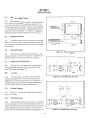
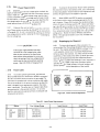
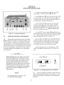
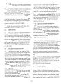


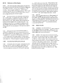
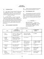


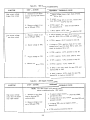

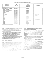

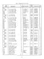


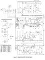


![() [IT] LK/S 4.2](http://vs1.manualzilla.com/store/data/006135181_1-b116a464f76fc09be64d6bd073b26233-150x150.png)