1
Errata
Title & Document Type: 6433B DC Power Supply Module Operating
and Service Manual
Manual Part Number: 06433-90001
Revision Date: January 1966
About this Manual
We’ve added this manual to the Agilent website in an effort to help you support your
product. This manual provides the best information we could find. It may be incomplete
or contain dated information, and the scan quality may not be ideal. If we find a better
copy in the future, we will add it to the Agilent website.
HP References in this Manual
This manual may contain references to HP or Hewlett-Packard. Please note that HewlettPackard's former test and measurement, life sciences, and chemical analysis
businesses are now part of Agilent Technologies. The HP XXXX referred to in this document is
now the Agilent XXXX. For example, model number HP8648A is now model number Agilent
8648A. We have made no changes to this manual copy.
Support for Your Product
Agilent no longer sells or supports this product. You will find any other available
product information on the Agilent Test & Measurement website:
www.agilent.com
Search for the model number of this product, and the resulting product page will guide
you to any available information. Our service centers may be able to perform calibration
if no repair parts are needed, but no other support from Agilent is available.
OPERATING AND SERVICE MANUAL
MODEL 64330
DC POWER SUPPLY
MANUFACTURING CODE 6A
January, 1966
TABLE OF CONTENTS
Section
Title
Page
. . . . . . . . . . . . . . . . . . . 1-1
. . . . . . . . . . . . . . . . . . . . . . 1-1
. . . . . . . . . . . . . . . . . . . . . . 1-1
. . . . . . . . . . . . . . . . . 1-1
. . . . . . . . . . . . . . . . . . . . . . 1-1
. . . . . . . . . . . . . . . . . . . . .1-1
. . . . . . . . . . . . . . . . . . 1-1
. . . . . . . . . . . . . . . . 1-2
GENERAL INFORMATION
1.1
Description
1.2
General
1.4
Overload Protection
1.7
Cooling
1.9
Monitoring
1.11
Output Terminals
1.
13 Instrument Identification
.
.
.
.
.
.
.
. . . . . . . . . . . . . . . . . . . . . . . 2.1
. . . . . . . . . . . . . . . . . . . 2-1
. . . . . . . . . . . . . . . . . . . . . . 2.1
. . . . . . . . . . . . . . . . .2 - 1
. . . . . . . . . . . . . . . . . . .2-1
. . . . . . . . . . . . . . . . . . 2-1
. . . . . . . . . . . . . . . . . . . . . .2.1
. . . . . . . . . . . . . . . . . . . . .2.1
. . . . . . . . . . . . . .2-2
. . . . . . . . . . . . . . . . . . . .2-2
. . . . . . . . . . . . . . . . 2-2
INSTALLATION
2.1
Initial Inspection
2.2
General
2.4
Mechanical Check
2.6
Electrical Check
2.8
Installation Data
Genera1
2.9
2.11
Location
2-13
Power Requirements
2.15
Power Cable
2.18 Repackaging for Shipment
.
.
.
.
.
.
..
.
.
. . . . . . . . . . . . . . . . . . 3.1
. . . . . . . . . . . . . . . 3-1
. . . . . . . . . . . . . . . . . . . . . .i.3
. . . . . . . . . . . . . . . . . . . . . .3.1
. . . . . . * . . . . . . . . . . . . . . . . .3.1
. . . . . . . . . . . . . . . . . . .3-2
. . . . . . . . . . . . . . . . . . .3.2
. . . . . . . . . . . . . . . . . 3-3
. . . . . . . . . . . . . . . . . . . . . 3.5
. . . . . . . . . . . . . . . . . . . . . . . 3.5
. . . . . . . . . . . . . . . . . . . . 3-6
. . . . . . . . . . . . . . . . 3-7
. . . . . . . . . . . . . . . . . . . . 3.7
. . . . . . . . . . . . . . . . .3.7
. . . . . . . . . . . . . . . .3-7
. . . . . . . . . . . . . . .3.7
OPERATING INSTRUCTIONS
31.
Controls and Indicators
3.3
Operation
3.4
Genera1
3-6
Normal
3- 10
Connecting Load
3.14
Remote Sensing
3.17
Remote Programming
3.26
Parallel
3.30
Series
3 .35
Auto-Tracking
3-3 8 Operating Considerations
3.39
Pulse Loading
3.41
Output Capacitance
3.44
Negative Voltage Loading
Negative Current Loading
3.46
.
.
...
.
.
.
.
.
.
.
.
.
.
.
TABLE OF CONTENTS (cont )
Title
Section
IV
. . . . . . . . . . . . . . . . . .4.1
. . . . . . . . . . . . . . .4.1
. . . . . . . . . . . . . . . . . .4.2
. . . . . . . . . . . . . . . . . . . .4.2
. . . . . . . . . . . . . . . . . . . .4.2
. . . . . . . . . . . . . . . . .4.2
. . . . . . . . . . . . . . . . . . . .4.3
. . . . . . . . . . . . . . . . . . . 4.4
. . . . . . . . . . . . . . . . . . .4.4
. . . . . . . . . . . . . . . .4.4
. . . . . . . . . . . . . .4.6
. . . . . . . . . . . . . .4.6
PRINCIPLES OF OPERATION
4.1
Block Diagram Description
4.9
Circuit Description
4.10
AC Input
4.12
DC Output
VoltageInput
4.14
4.20
Current Input
4.24
Gating Circuit
4.27
Turn.OnCircuit
4.29
SCR Regulator Control
4-3 7
SCR Regulator
4.42
Bias and Reference Circuit
.
.
.
.
.
.
.
..
.
.
. . . . . . . . . . .
MAINTENANCE
5.
1
General
5.3
Measurement Techniques
5.7
Performancecheck
5.8
General
Rated Output and Meter Accuracy
5- 10
5.
13
Line Regulation
Load Regulation
5.
16
5.19
Ripple and Noise
Transient Recovery Time
5 -2 1
5.23
Additional Specification Check
5 -24
Temperature Coefficient
5-2 7
Output Stability
5 -3 0
Remote Programming
5-33
Output Impedance
5-3 5
Output Inductance
5-3 7 Cover Removal
5.39
Troubleshooting
5.40
General
5.42
Trouble Analysis
5.49
Repair and Replacement
5.51
Adjustments and Calibrations
5 -5 2
General
5.54
Meterzero
5.56
Voltmeter Tracking
5.58
Ammeter Tracking
Constant Voltage Programming Current
5 .60
5.62
Zero Voltage Output
Constant Current Programming Current
5 -64
.
.
.
..
.
.
.
.
..
.
.
.
.
..
.
..
.
.
.
..
.
.
.
Page
..............
......
.........
.............
..
..........
.........
.........
......
....
. . . . .
..........
........
.........
.........
...........
...........
.............
.........
.......
.....
.............
............
.........
.........
........
.
TABLE OF CONTENTS (cont )
Section
Page
Title
.
.
5 .66
5.68
5.70
.
.
5.72
. . . . . . . . . . . . . . . . .5-16
. . . . . . . . .5 .16
. . . . . . . . . . . . . . . . . .5.17
Zero Current Output
Bias and Reference Line Regulation
Line Imbalance
Constant Current Load Regulation
. . . . . . . . . . .5.18
. . . . . . . . . . . . . . . . . . . . .6 .1
. . . . . . . . . . . . . . . .6.1
. . . . . . . . . . . . . . . . . .6.1
REPLACEABLE PARTS
6.1
Introduction
6.4
OrderingInformation
..
.
iii
MODEL 6433B
REVISION:
Please note the following changes in the instruction manual:
1, Wherever 64334 appears, change it to 64338.
2.
Eliminate the 10A fuse and holder in the ACC side of the line.
3.
Change voltage rating from 32 volts t o 36 volts.
4, Change T 1 from 643391 t o 643391B.
5. Change C13 and C17 from 47, OOOpf 40VDC to 40,000pf 50VDC Mfg, Part # D42343.
6, Change R21 from 160 ohm 2W t o 43 ohm 2W.
7, Remove C12 from AC lead
8, Change Q1,2,3,4,6,8,9
--
move to ACC (anode of CR18).
from 2N3390 to 2N3391 Corporate Part # 1854-0071.
Table 1-1
.
Specifications
r
J
INPUT:
105-125 vac, 57 t o 63 c p s , single phase,
7 amperes, 450 watts max
RATED OUTPUT:
Constant Voltage: 0 t o 32 vdc.
Constant Current: 0 t o 10 amperes d c
LINE REGULATION:
Constant Voltage:
105-125 v a c input
Constant Current:
105-125 v a c input
LOAD REGULATION:
Constant Voltage: Less than 36 mv for 0
t o 10ampere load change.
Constant Current: Less thari 100 ma for 0
t o 3 2 vdc load change.
RIPPLE AND NOISE:
32 mvrms
OPERATING TEMPERATURE RANGE:
O°C t o 50°c
STORAGE TEMPERATURE RANGE:
-20°C t o 71%
TEMPERATURE COEFFICIENT:
Constant Voltage: 0.05% plus 8 mv per
degree centigrade.
30 ma per degree
Constant Current:
centigrade.
OUTPUT STABILITY:
(after 30-minute warm-up)
Constant Voltage: 0.15% plus 2Bmv for 8
hours a t constant temperature.
Constant Current: 1OOma for 8 hours a t
constant temperature.
REMOTE PROGRAMMING:
Constant Voltage: 2 00 ohms per volt *1%
Constant Current: 2'5ohms per ampere +10%
TYPICAL OUTPUT IMPEDANCE:
Less
Less
Less
Less
OUTPUT INDUCTANCE:
1.0 microhenry
.
than
than
than
than
L e s s than 18 mv for
change.
Less than 1 ODma for
change.
0.01 ohm from d c t o 0.5 c p s
0.5 ohm from 0.5 c p s t o 100 c p s
0.2 ohm from 100 c p s t o l k c
1.0 ohm from l k c t o 100 k c
Table 1-1
TRANSIENT RECOVERY TIME:
.
Specifications (cont .)
In constant voltage operation, l e s s than
300 milliseconds is required for output
voltage recovery t o within 200millivolts
of the nominal output voltage following a
load change equal t o one half t h e maximum
current rating of the power supply.
Nominal output voltage is defined a s t h e
mean between t h e no-load and full-load
voltages. The transient amplitude is l e s s
than 0 . 5 volt per ampere for any load
change between 20% and 100% of rated
output current. (Excluding the initial spike
of approximately 100 microseconds duration which is significant only for load r i s e
times faster than 0.5 ampere per microsecond )
.
SIZE AND WEIGHT:
Heiaht
3-1/2in.
Width
19in.
FINISH:
Light gray front panel with dark gray c a s e .
Depth
17-1/2in.
Figure 1-1. Model 6433ADC Power Supply
Weight
33 lb.
SECTION I
GENERAL INFORMATION
1- 1.
-
DESCRIPTION
1-2.
GENERAL
1-3.
The H-Lab Model 6433ADC Power Supply (fig. 1-1) i s a completely solidstate, compact, well-regulated, constant voltage/constant current d c power supply
suitable for either bench or relay rack operation. A three-wire five-foot power cord
is provided. The output is continuously variable between 0 and 32vdc, and between 0 and 10 amperes. Detailed specifications are given in table 1-1
.
1-4.
OVERLOAD PROTECTION
A crossover feature protects both power supply and load in constant voltage
1-5.
operation. Automatic crossover circuitry switches the power supply from constant
voltage to constant current operation i f the output current exceeds a preset limit.
This crossover circuitry a l s o protects the load from overvoltage during constant
current operation by automatically switching the power supply into constant voltage
operation. The user can adjust the crossover point via the front panel controls
(para. 3 -8 and 3-9)
.
The power supply is protected from reverse voltage (positive voltage applied
1-6.
t o negative terminal) by a diode that shunts current across the output terminals
when this condition exists. The a c input is fused. A double-pole on/off switch
opens both power leads in the off position.
1-7.
COOLING
1-8.
Convection cooling is used. No fan is required. The power supply has no
moving parts (except meter movement).
1-9.
MONITORING
1-10. Two front-panel meters are provided for monitoring output voltage and current.
The voltmeter has a 0 to 40 volt range and the ammeter has a 0 t o 12 ampere range.
Each meter has a 2% accuracy a t full scale.
1-1 1.
OUTPUT TERMINALS
1-12. Output power is available via a terminal strip on the rear panel. The rear
panel terminal strip a l s o enables the power supply t o be connected for different
modes of operation (para. 3-3). The output terminals gre isolated from the c h a s s i s
and either t h e positive or the negative terminal may be connected t o the c h a s s i s
via a separate ground terminal located adjacent t o the output terminals. The power
supply is insulated t o permit operation up t o 3 0 0 vdc off ground.
1-- 13
.
INSTRUMENT IDENTIFICATION
Harrison Laboratories power supplies a r e identified by a three-part designation. The first part is the model number: the second part is the serial number: and
the third part is the manufacturing code letter. This manual applies t o all Model
'6433A power supplies with the same manufacturing code letter given in the title
page. Change sheets will be supplied with the manual t o make it apply t o Model
6433A power supplies with different manufacturing code letters.
1-14.
SECTION I1
INSTALLATION
2 - 1.
INITIAL INSPECTION
2-2.
GENERAL
Before shipment, the power supply was inspected and found free of mechan2-3.
ical and electrical defects. If damage to the shipping carton is evident, ask that
the carrier's agent be present when the power supply is unpacked. As soon a s the
power supply is unpacked, inspect i t for any damage that may have occurred in
transit. Also check t h e cushioning material for signs of severe stress (may be
indication of internal damage). Save all packing materials until the inspection is
completed. If damage is found, proceed a s instructed in t h e Claim for Damage in
Shipment notice on t h e back of the front cover of this manual.
2 -4.
MECHANICAL CHECK
2-5.
Check that there are no broken knobs or connectors, that the external surface is not scratched or dented, that the meter faces are not damaged, and that a l l
controls move freely. Any external damage may be a n indication of internal damage.
2 -6..
ELECTRICAL CHECK
2-7.
Check that the straps on the terminal strip a t the rear of t h e power supply
are secure and that the strapping pattern is in accord with figure 3-2. Check t h e
electrical performance of the power supply a s soon a s possible after receipt. A
performance check that i s suitable for incoming Jnspection is given in paragraphs
5 -7 through 5 -2 2
.
2 -8
2-9.
.
INSTALLATION DATA
GENERAL
2-10. The power supply is shipped ready for bench or relay rack (19 inch)
opera tion.
-
2 11. LOCATION
Because the power supply is cooled by convection, there must be enough
2-12.
space along the sides and rear of the power supply t o permit free flow of cooling
air. The power supply should be located in an area where the ambient temperature
does not exceed 50°c.
2 -13.
POWER REQUIREMENTS
The power supply is operated from a 105 to 125 volt (115 volts nominal),
57 to 6 3 cps, single phase power source. At 115 volts, 6 0 cps, the full load requirement is 450 watts a t 6.5 amperes.
2-14.
2-15.
POWER CABLE
2 - 1 6 . To protect operating personnel, the National Electrical Manufacturers
Associa tion (NEMA) recommends that the instrument panel and cabinet be grounded.
This instrument is equipped with a three-conductor power cable. The third conductor is the ground conductor and when the cable is plugged into an appropriate
receptacle, the instrument is grounded. The offset pin on the power cable threeprong connector is the ground connection.
2-17.
To preserve the protection feature when operating the instrument from a twocontact outlet, u s e a three-prong to two-prong adaptor and connect the green lead
on the adaptor t o ground.
-
2 18.
REPACKAGING FOR SHIPMENT
2-19.
To insure s a f e shipment of the instrument, it is recommended that the package designed for the instrument be used. The original packaging material is reusable. If i t is not available, contact your Hewlett-Packard field office for packing
materials and information. A packing carton part number is included in the parts
list.
2 - 2 0 . Attach a tag t o the instrument which specifies the owner, model number, full
serial number, and service required, or a brief description of the trouble.
PILOT
LIGHT
1
OFF/ON
SWITCH
VOLTMETER
ZERO-SET
/
/
COARSE
VOLTAGE
SINE
VOLTAGE
AMMETER
Ice
ARsE
CURRENT
\
FINE
CURRENT
1. TURN O N POWER SUPPLY
2. ADJUST OUTPUT VOLTAGE
3. OBSERVE VOLTMETER
4. SHORT OUTPUT TERMINALS (AT REAR OF POWER SUPPLY) AND ADJUST OUTPUT
CURRENT LIMIT
5 . OBSERVE AMMETER
6. REMOVE SHORT AND CONNECT LOAD TO OUTPUT TERMINALS
Figure 3-1.
Controls a n d Indicators
SECTION I11
OPERATING INSTRUCTIONS
3-1.
CONTROLS AND INDICATORS
3-2.
The controls and indicators are illustrated in figure 3-1.
3 -3
.
3-4.
OPERATION
GENERAL
3-5.
The power supply is designed s o that i t s mode of operation can be selected
by making strapping connections between particular terminals on the terminal strip
a t t h e rear of the power supply. The terminal designations a r e stenciled in white on
the power supply and a r e adjacent to their respective terminals. The strapping
patterns illustrated in this section show neither terminal grounded. The operator
c a n ground either terminal or operate the power supply up to 300 vdc off ground
(floating)
.
3-6.
NORMAL
3-7.
GENERAL. The power supply is normally shipped with its rear terminal
strapping connections arranged for constant voltage/constant current, local sensing, local programming, single unit mode of operation. This strapping pattern is
illustrated in figure 3-2. The operator selects either a constant voltage or a
constant current output using the front panel controls (local'programming, no strapping changes a r e nece ssary)
.
3-8.
CONSTANT VOLTAGE. To select a constant voltage output, proceed a s
follows :
a . Turn-on power supply and adjust VOLTAGE controls for desired output
voltage (output terminals open).
b. Short output terminals and adjust CURRENT controls for maximum output
current allowable (current limit), a s determined by load conditions. If a load change
causes t h e current limit to be exceeded, the power supply will automatically crossover t o constant current output a t the preset current limit and the output voltage will
drop proportionately. In setting the current limit, allowance must be made for high
peak currents whichocan c a u s e unwanted cross-over (refer t o para. 3-40).
%
3-9.
CONSTANT CURRENT. To select a constant current output, proceed a s
follows :
a . Short output terminals and adjust CURRENT controls for desired output
current.
b. Open output terminals and adjust VOLTAGE controls for maximum output
voltage allowable (voltage limit), a s determined by load conditions. If a load
change c a u s e s the voltage limit to be exceeded, the power supply will automatically crossover to constant voltage output a t t h e preset voltage limit and the output
current will drop proportionately. In setting the voltage limit, allowance must be
made for high peak voltages which can c a u s e unwanted crossover. (Refer t o
para. 3 -4 0 .)
3-10.
CONNECTING LOAD
3-11. Two pairs of output terminals are provided on the terminal strip a t the left
rear side (facing rear) of the power supply. Either pair of terminals or both may be
used. The terminals are marked + and
A separate ground terminal is located
adjacent t o the output terminals. The positive or negative output terminal may be
grounded, or neither grounded (floating operation: permitted to 3 0 0 vdc off ground)
-.
.
3-12. Each load should be connected to the power supply output terminals using
separate pairs of connecting wires. This will minimize mutual coupling effects
between loads and will retain full ~ d v a n t a g eof the low output impedance of the
power supply. Each pair of connecting wires should be a s short a s possible and
twisted or shielded to reduce noise pickup. (If shield is used, connect one end t o
power supply ground terminal and leave the other end unconnected.)
3-13. If load considerations require that t h e output power distribution terminals
be remotely located from the power supply, then the power supply output terminals
should be connected t o the remote distribution terminals via a pair of twisted or
shielded wires and each load separately connected t o the rem ote distribution
terminals. For this c a s e , remote sensing should be used (para. 3-14).
NOTE
It is recommended that the voltage drop i n the connecting wires not exceed 2 volts. If a larger drop
must be tolerated, please consult a Hewlett-Packard
field representative.
3-14.
REMOTE SENSING
3-15. Remote sensing is used to ameliorate the degradation of regulation which
will occur a t the load when the voltage drop in the connecting wires is appreciable.
The u s e of remote distribution terminals (para. 3- 13) i s a n 'example where remote
sensing may be required. Due to the voltage drop in the load leads, i t may be
necessary to slightly increase the current limit in constant voltage operation.
CAUTION
Turn-off power supply before rearranging strapping pattern at the power supply rear terminal
strip. If the - S terminal is opened while the
power supply is on, the output voltage and current may exceed their maximum ratings and result in damage t o the load. The power supply
will not be damaged.
3-16.
Proceed a s follows:
a . Turn-off power supply and arrange rear terminal strapping pattern a s
shown in figure 3-3. The sensing wires will carry l e s s than 10 ma and need not be
a s heavy a s the load wires. It is recommended that sensing and load wires be
twisted and shielded. (If shield is used, connect one end to power supply negative
terminal and leave the other end unconnected .)
CAUTION
Observe polarity when connecting the sensing
leads t o t h e load.
b. In order t o maintain low a c output impedance, a capacitor with a minimum rating of 20,00Op,fd and 25 vdcw should be connected across the load using
short leads. This capacitor must have high-frequency characteristics a s good or
better than C17 h a s (see parts l i s t ) .
c
3 -17.
. Turn-on
power supply.
REMOTE PROGRAMMING
3-18. GENERAL. The constant voltage and constant current outputs may be programmed (controlled) from a remote location, The front-panel controls are disabled
in the following instructions. Changes in the rear terminal strapping arrangement
a r e necessary. The wires connecting the programming terminals of the power supply
t o t h e remote programming device should be twisted or shielded to reduce noise
pick-up. (if shield is used, connect one end t o power supply ground terminal and
leave t h e other end unconnected .) Remote sensing (para. 3 - 14) may be used simultaneou sly with remote programming. However, the strapping patterns shown in
figures 3-4, 3-5, and 3-6 employ only local sensing and do not show the load
connections.
CAUTION
Turn-off power supply before rearranging strapping pattern a t the power supply rear terminal
strip. If the current programming terminals are
opened while the power supply is on, the output current will exceed i t s maximum rating and
may result in damage t o t h e load. The power
supply will not be damaged. The constant voltage programming terminals have a Zener diode
connected internally across them to limit t h e
programming voltage and thus prevent excessive
output voltage.
3-19. CONSTANT VOLTAGE. In t h e constant voltage mode of operation, either a
resistance or voltage source can b e used for remote programming. For resistance
programming, the programming coefficient (fixed by the programming current) is
200 ohms per volt (output voltage increases 1 volt for each 200 ohms in series with
programming terminals). The programming current is adjusted to within 1%of 5 ma
a t the factory. If greater programming accuracy is required, change R39 (shunt).
The programming resistance should be a stable, low noise, low-temperature (less
than 30 ppm per OC) resistor with a power rating a t least 10 times i t s actual dissipation.
3-20. The output voltage of the power supply s,hould be 0 t 2 0 mv, -100 mv when
the programming resistance is zero ohms. This tolerance can be improved by changFor further information on improving this tolerance, refer to paragraph 5 -63
ing R 6
and t o H-Lab Tech Letter #l.
.
3-2 1. If the resistance programming device is controlled by a switch, make-beforebreak contacts should be used i n order t o avoid momentary opening of the programming terminals, To connect the remote programming resistance, arrange rear
terminal strapping pattern a s shown in figure 3-4. The front-panel VOLTAGE
controls a r e disabled when the strap between A6 and A7 is removed.
3-22. If a voltage source is used a s the remote programming device, t h e output
voltage of t h e power supply will vary in a 1 to 1 ratio with the programming voltage.
The load on the voltage source will not exceed 25 microamperes. To connect the
programming voltage, arrange rear terminal strapping pattern a s shown in figure 3-5.
.
3 -23
CONSTANT CURRENT. In constant current operation, resistance programming is used. The r e s i s t ~ c programming
e
coefficient (fixed by the programming
current) is 25ohms per ampere (output current increases 1 ampere for each 2 5 ohms
in series with programming terminals). The programming current is adjusted to
within approximately 10% of 4 ma a t the factory. If greater,programming accuracy
is required, change R41 (shunt). The programming resistance should be a stable,
low noise, low-temperature ( l e s s than 30 ppm per OC) resistor with a power rating
a t least 10 times its actual dissipation.
3-24. The output current of the power supply should be 0 t 50 ma, -1:OO ma when
the programming resistance is zero ohms. This tolerance can be improved by changing ~ 2 0 .For further information on improving this tolerance, refer to paragraph
5-6 7 and t o H-Lab Tech Letter #l
.
3-25. If the resistance programming device is controlled by a switch, makebefore-break contacts should be used t o avoid momentary opening of the programming terminals. To connect the remote programming resistance, arrange rear termina l strapping a s shown in figure 3-6. The front-panel CURRENT controls are disabled
when the strap between A 1 and A2 is removed.
3 -2 6 .
PARALLEL
3-27. GENERAL. Two or more power supplies can be connected in parallel t o
obtain a total output current greater than that available from one power supply.
The total output current is the sum of the output currents of the individual power
supplies. Each power supply c a n be t urned-on or off separately. Remote sensing
(para. 3 - 14) and programming (para. 3 -17) can be used; however, the strapping
patterns shown in figures 3-7 and 3 - 8 employ only local sensing and programming.
3-28. NORMAL. The strapping pattern for normal parallel operation of two power
supplies is shown in figure 3-7. The output current controls of each power supply
can be separately s e t . The output voltage controls of one power supply (master)
should be s e t to the desired output voltage; the other power supply (slave) should
be s e t for a slightly larger output voltage. The master will a c t a s a constant
voltage source; the slave will act a s a constant current source, dropping i t s output
voltage to equal t h e master's.
.
3 -2 9 AUTO-PARALLEL. The strapping patterns for auto-parallel operation of two
and three power supplies are shown in figures 3-8A and B, respectively. Autoparallel operation permits equal current sharing under a l l load conditions, and
allows complete control of output current from one master power supply. The output
current of each slave is approximately equal to the master's. Because the output
current controls of each slave is operative, they should be s e t to maximum to avoid
having the slave revert t o constant current operation: this would occur i f the master
output current setting exceeded the s l a v e ' s .
3-30.
SERIES
3 -3 1. GENERAL. Two or more power supplies can be connected in series t o obtain
a total output voltage higher than that available from one power supply. The total
output voltage is t h e sum of t h e output voltages of the individual power supplies.
A single load can be connected across the series-connected power supplies or a
separate load can be connected across each power supply. The power supply has
a reverse polarity diode connected internally across the output terminals t o protect
the power supply against reverse polarity voltage if the load is short-circuited or
if one power supply is turned off while i t s series partners are on.
3-32. The output current controls of each power supply a r e operative and the current limit is equal t o t h e lowest control setting. If any output current controls a r e
s e t too low with respect t o t h e total output voltage, the s e r i e s power supplies will
automatically crossover t o constant current operation and the output voltage will
drop. Remote sensing (para. 3-14) and programming (para. 3- 17) c a n be used;
however, the strapping patterns shown i n figures 3-9 and 3-10 employ only local
sensing and programming.
3-33. NORMAL. The strapping pattern for normal s e r i e s operation of two power
supplies is shown in figure 3-9. The output voltage controls of each power supply
must be adjusted t o obtain the total output voltage.
3 -34. AUTO-SERIES. The strapping patterns for auto-series operation of two and
three power supplies a r e shown in figures 3-10A and B, respectively. Auto-series
operation permits control of t h e output voltage of several power supplies (slaves)
from one master power supply. The master must b e the most negative power supply
of t h e s e r i e s . To obtain positive and negative voltages, t h e terminal of t h e master may b e grounded. For a given position of t h e s l a v e output voltage controls, t h e
total output voltage is determined by the master output voltage controls. The output
voltage controls of a slave determines t h e percentage of t h e total output voltage
that t h e s l a v e w i l l contribute. Turn-on and turn-off of t h e s e r i e s is controlled by
the master. In order t o maintain the temperature coefficient and stability specifications of t h e power supply, t h e external resistors shown in figures 3-10A and B,
should be stabie, low-noise, low-temperature (less than 30 ppm per OC) resistors.
The value of t h e s e resistors is determined by multiplying t h e output voltage of t h e
applicable s l a v e by t h e programming coefficient (2 00 ohms/volt)
+
.
3 -3 5 . AUTO-TRACKING
3-36. The strapping patterns for auto-tracking operation of two and three power
j ~ p p l i e sa r e shown in figures 3-llA and B, respectively. Automatic tracking
s.,:!eration permits t h e output voltages of two or more power supplies t o b e referenced t o a common buss; one of t h e power supplies (master) controls t h e magnitude of
the output voltage of t h e others (slaves) for a given position of the s l a v e output
voltage controls. The master must be t h e most negative power supply in t h e group.
The output voltage of a s l a v e is a percentage of t h e master output voltage. The
output voltage controls of a s l a v e determines t h i s percentage. Turn-on and turnoff of t h e power supplies is controlled by t h e master. Remote sensing (para. 3-14)
and programming (para. 3 - 17) c a n be used; however, t h e strapping patterns shown
in figure 3 -4 employ only local sensing and programming.
3-37. The value of t h e external resistors shown in figure 3-11 is determined by
dividing t h e voltage difference between t h e master and the applicable slave by t h e
programming current (nominally 5 ma; refer t o para. 3-19). Finer adjustment of the
s l a v e output voltage c a n be accomplished using t h e s l a v e output voltage controls.
In order t o maintain t h e temperature coefficient and stability specifications of t h e
power supply, the external resistors should b e stable, low-noise, low-temperature
( l e s s than 30 ppm per OC) resistors.
3 -3 8 .
OPERATING CONSIDERATIONS
3 -3 9.
PULSE LOADING
3-40. The power supply will automatically cross over from constant voltage to
constant current operation, or the reverse, in respone t o an increase (over the
preset limit) in t h e output current or voltage, respectively. Although the preset
limit may be s e t higher than the average output current or voltage, high peak
currents or voltages ( a s occur i n pulse loading) may exceed the preset limit and
c a u s e crossover t o occur. To avoid this unwanted crossover, t h e preset l i m i t must
be set for the peak requirement and not the average.
3 -4 1 .
OUTPUT CAPACITANCE
3-42. There are capacitors (internal) across t h e output terminals of the power
supply. These capacitors help t o supply high-current pulses of short duration
during constant voltage operation. Any capacitance added externally will improve
the pulse current capability, but will decrease the safety provided by the constant
current circuit. A high-current pulse may damage load components before the
average output current is large enough to c a u s e t h e constant current circuit t o
operate.
3 - 4 3 . The effects of the output capacitors during constant current operation a r e
a s follows:
a . The output impedance of t h e power supply decreases with increasing
frequency.
b.
The r i s e t i m e of the output voltage is increased.
c. A large surge current causing a high power dissipation in the load occurs
when t h e load impedance is reduced rapidly.
NEGATIVE VOLTAGE LOADING
3 - 4 5 . A diode is connected across t h e output terminals. Under normal operating
conditions, the diode is reverse biased (anode connected to negative terminal). If
a negative voltage is applied t o t h e output terminals (positive voltage applied t o
negative terminal), t h e diode will conduct, shunting current across the output terminals and limiting the voltage t o t h e forward voltage drop of t h e diode. This diode
protects the filter and output electrolytic capacitors.
I
3 -46.
NEGATIVE CURRENT LOADING
3 - 4 7 . Certain types of loads may c a u s e current t o flow into the power supply in the
direction opposite t o the output current. If the reverse current exceeds 0 .It ampere,
preloading will be necessary. For example; i f t h e load delivers 1 ampere t o the
power supply with the power supply output voltage a t 18 vdc, a resistor equal t o
18 ohms (18v/la) should be connected across the output terminals. Thus, the
18 ohm resistor shunts the reverse current across the power supply. For more
information on preloading, refer to paragraph C4 in the H-Lab Application Manual.
FIGURE 3-2. NORMAL STRAPPING PATTERN
I
I
FIGURE 3-3.
REMOTE SENSINO STRAPPINO PATTERN
PROGRAMMING
RESISTOR
FIGURE 3-4.
REMOTE RESISTANCE
PROGRAMMING(C0NSTANT VOLTAOE)
STRAPPING PATTERN
FIGURE 3-5. REMOTE VOLTAGE
PROGRAMMING (CONSTANT VOLTAGE)
STRAPPING PATTERN
'OURCE
PROGRAMMING
RESISTOR
FIGURE 3-6. REMOTE RESISTANCE PROGRAMMING
(CONSTANT CURRENT) STRAPPING PATTERN
l & ! b ~ ~ ~ ~6 ~ 6! 7 ~ 6 ~ ~
SLAVE
+
+
G
-
-
AI
A 2 A3 A 4 - 3
-
+
+S
AS A 6 A 7
FIGURE 3 - 7 WORMAL PARALLEL STRAPPING PATTERN
MASTER
SLAVE 1
SLAVE
A.TWO POWER SUPPLIES
+ + m - -
A1
AS A3 A 4 -S
- + +S
0. THREE POWER SUPPLIES
FIGURE 3-8. AUTO- PARALLEL STRAPPING PATTERN
A5 A 6 A 7
+ + a - -
- +
A1 A 2 A 3 A 4 - S
+S AS A 6 A7
+
+
G
-
-
A1
A2 A3 A 4 -9
- +
+S
AS A6 A 7
AI
A 2 A3 A 4 -S
- + +S
A5 A 6 A7
MASTER
+
+
G
-
-
Al
- +
A 2 A3 A 4 -S
SLAVE
+S
+ + a - -
A5 A 6 A7
A. TWO POWER SUPPLIES
FIGURE 3-9.
NORMAL SERIES STRAPPING PATTERN
+ + a - MASTER
SLAVE I
FIGURE
AUTO-SERIES
STRAPPING
PATTERN
SLAVE 2
8. THREE POWER SUPPLIES
+ + a - -
A1 A 2 A 3 A 4 - 9
- +
+S A 5 A 6 A 7
MASTER
(MUST BE
MOST NEGATIVE )
lelOlolelblalblol
SLAVE
A. TWO POWER SUPPLIES
+
+
G
-
-
A1 A 2 A 3 A 4 - S
- +
+S A 5 A 0 A 7
MASTER
(MUST BE
MOST NEGA T lVE
SLAVE I
FIGURE. 3-11 AUTO-TRACKING
STRAPPING
PATTERN
el-AVE 2
..
.-
a
AC
INPUT
a
T
,
POWER
TRANSFORMER
f
SCR
SCR
REGULATOR
4
CONTROL
t
REGULATOR
I -
+ AUX.
-
B
w
+
--)
FIGURE 4-1.
BLOCK DIAGRAM
CIRCUIT
TURN ON
-
4
-
MAIN
RECTIFIER
8 FILTER
GATING
CIRCUIT
.
I
MAIN
POWER
TRANS) FORMER
REFERENCE
CIRCUIT
BIAS
,
I
-
DC
R9, RIO
CURRENT
CONTROL
VOLTAGE INPUT
CIRCUIT
R23
CURRENT
MONITORING
RESISTOR
41
1
CURRENT INPUT
CIRCUIT
SECTION IV
PRINCIPLES OF OPERATION
4-1.
BLOCK DIAGRAM DESCRIPTION (See figure 4-1 .)
4-2.
The main power transformer isolates the a c input from the power supply and
reduces i t t o the voltage level required. Rectification and filteri,ng produces a
smoothed d c output across the - and + terminals. A large capacitor (Co) i s connected across the - and + terminals for low a c output impedance and t o help supply large
pulse currents. An SCR regulator controls the a c input t o provide good regulation
of the d c output. The auxiliary power transformer powers the SCR regulator control
circuit and the bias and reference circuit which produces d c bias and reference
voltages for the power supply.
The SCR regulator is controlled by the SCR regulator control circuit which
4-3.
operates in response to signals developed by the voltage or current input circuit.
A gating circuit assures that only one input circuit i s used a t a time.
4-4.
The voltage and current input circuits operate in a similar manner. Each
circuit h a s a differential amplifier that amplifies a n error voltage that is proportiona l t o the difference between the actual output and the programmed output. The
programmed output is determined by the resistance of t h e programming resistors
(voltage and current controls). Each programming resistor has a constant current
through i t which is maintained by the bias and reference circuit.
4-5.
The voltage input circuit differential amplifier detects the error voltage
that is proportional t o the difference between the voltage across its programming
resistors (R2-R8) and the d c output voltage. The error voltage is amplified and
passed through the gating circuit t o the SCR regulator control which triggers the
SCR regulator. The SCR regulator increases or decreases the a c input voltage t o
the main power transformer a s required to maintain a constant load voltage that is
equal t o the programmed voltage. In constant voltage operation, the gating circuit
i s biased t o inhibit the input from the current input circuit.
The current input circuit differential amplifier detects the error voltage that
4-6.
i s proportional t o the difference between the voltage across i t s programming
resistors (R9-R10) and the voltage across current monitoring resistor R23 The
voltage across R23 is proportional t o the load current. The SCR regulator responds
t o the amplified error voltage by increasing or decreasing the a c input current t o
the main power transformers a s required t o maintain a constant load current. In
constant current operation, t h e gating circuit i s biased t o inhibit the input from the
voltage input Circuit.
.
To prevent overvoltage and excessive surge current when the power supply
is turned-on, the turn-on circuit establishes initial conditions in the gating circuit.
The turn-on circuit is activated by the bias and reference circuit when the power
supply is turned-off.
4-7.
-
4-8.
A voltmeter is connected across the and + terminals t o monitor the output
voltage. An ammeter is connected across current monitoring resistor R23 t o monitor
the output current (proportional t o voltage across R23).
4-9.
CIRCUIT DESCRIPTION (See figure 4-2 a t back of manual.)
4-10.
AC INPUT
4-11. The 105-125 vac, 57-63 cps, single phase input is applied t o transformer
T2 and t o the series combination of transformer T1 and SCR's CR17 and CR18 which
are in parallel opposition. The SCR's a r e used t o regulate the d c output by controlling the average value of the a c input to transformer T I . Capacitors C11 and C12
smooth transients t o prevent the SCR's from being triggered by a rapidly changing
voltage from anode to cathode. Resistor R21 damps oscillations that may occur due
t o resonance of C12 and the leakage inductance of T I . The leakage inductance of
T 1 limits the peak input current.
4-12.
DC OUTPUT
.
4-13
The output of the secondary of transformer T1 is full-wave rectified by
bridge rectifier CR19 through CR22 and filtered by pi-section filter C13, C 1 7,
and L1. Resistor R29 damps the parallel resonance of L1 and C17. The d c output
is regulated t o a constant value by the SCR's i n the a c input line. Capacitor C17
is the output capacitor. Diode CR23 is connected across the filtered d c output t o
protect t h e power supply from reverse voltage applied t o the output terminals.
Resistor R23 is the current monitoring resistor; the full load current flows through it.
Resistors R25 and R27 are used t o calibrate the voltmeter and ammeter, respectively.
4-14.
VOLTAGE INPUT
.
4-15
GENERAL. The voltage input circuit is basically a differential amplifier
(Ql-Q2) that detects any voltage difference between the programmed output voltage
and the actual output voltage. The differential amplifier output voltage varies in
proportion t o the power supply output voltage valiation.
4 -16. Q2 INPUT. Voltage divider R6-R47 maintains a slightly negative b a s e bias
t o ensure that t h e output voltage can be programmed to zero. The output of 92 i s
emitter-coupled (resistor R4) t o Q1.
4-17. Q1 INPUT. There are three inputs t o the base of Q1; one determined by the
programmed voltage (voltage controls ~ 2 - R 8 ) ,the second determined by t h e collector voltage of Q1 (negative feedback), and the third is from t h e positive s i d e of the
main rectifier. The collector current of Q1 is determined by the difference between
i t s base and emitter inputs. This difference i s a n error voltage that is proportiona l t o t h e difference between the programmed output voltage and t h e actual output
voltage. The negative feedback from collector t o base (C4, and R17-R18 in parallel)
improves the stability of the voltage-regulating feedback loop.
4-18. The input from t h e positive s i d e of t h e main rectifier (C1 and R1) improves
loop stability by making t h e differential amplifier insensitive to output voltage
variations of four c p s or greater. Below four c p s t h i s input is negligible. This
input is necessary because the phase shift of the pi-section output filter begins t o
become e x c e s s i v e aver four c p s Resistors R1 and R5 a r e arranged s o that t h e four
c p s input is isolated from t h e negative feedback input; and s o that necessary
impedance l e v e l s a r e obtained looking out from t h e b a s e of Q1. The collector output of Q1 is coupled t o t h e gating circuit.
.
4-19. CLAMPING. In order t o protect the differential amplifier, t h e b a s e of Q1 is
clamped with respect t o -S by diodes CR1 and CR2 t o prevent e x c e s s i v e b a s e volta g e in either direction. Diode CR1 clamps the b a s e t o approximately -0.7 vdc;
CR2 and the base-emitter junction of Q1 clamp t h e b a s e t o approximately +1.4 vdc.
Zener diode VRI clamps t h e programming terminals t o prevent a n e x c e s s i v e error
signal that would c a u s e e x c e s s i v e output voltage. This would occur, for example,
if the programming terminals were opened accidentally. To prevent overshoot when
the power supply switches from constant current t o constant voltage, diodes CR9
and CRlO clamp the collector of 91. Resistor R30 provides a small bleed current
for CR1O ,
4-2 0.
CURRENT INPUT
4-2 1. GENERAL. The current input circuit is basically a differential amplifier
(Q8-Q9) that detects any current difference between t h e programmed output current
(proportional t o voltage a c r o s s current controls) and the actual output current (proportional t o voltage a c r o s s current monitoring resistor R23). The differential
amplifier output voltage varies in proportion t o t h e output current variation.
4-22. Q8-Q9 INPUT. The input t o t h e differential amplifier (across b a s e s of 98Q9) is t h e voltage difference a c r o s s current controls R9-R10 and current monitoring
resistor R23. Because t h e programming current is constant in constant current
operation, t h e voltage input t o the differential amplifier varies a s t h e load current
through R23 (error voltage). Capacitors C6 and C24 and resistor R22 provide gain
roll-off a t high frequencies. Diode CR26 clamps the voltage ( 0 . 7 vdc) a c r o s s t h e
emitter-base junction of Q9 and R20.
his clamping action prevents e x c e s s i v e
reverse b a s e voltage in Q9 when very large load current is drawn (output terminals
shorted). To prevent overshoot when the power supply switches from constant
voltage t o constant current opleration, diodes CRlO and CR12 clamp t h e collector of
Q8
4-23. Q8-Q9 OUTPUT. Resistor R13 is t h e collector load for Q8. The collector
output of Q8 i s coupled t o t h e gating circuit. Voltage divider R20-R46 b i a s e s t h e
b a s e of Q9 and maintains a slightly negative b a s e bias t o ensure that the output
current c a n b e programmed t o zero. Resistor R44 provides positive feedback t o
improve load regulation during constant current operation.
4-24.
GATING CIRCUIT
4-25. Transistor Q4 draws current from t h e SCR control circuit (capacitor C25).
The magnitude of t h i s current is determined by either the voltage or current input
circuit. For constant voltage operation, diode CR7 is forward biased t o permit t h e
voltage input circuit t o drive Q4; diode CR8 is reverse biased t o inhibit the input
from t h e current input circuit. For constant current operation, t h e reverse occurs.
4-26. To prevent transients in the d c output when t h e power supply is turned-on,
t h e turn-on of Q4 i s delayed by capacitor C2 which charges throuqh R12, R15 and
CR5. When C2 charges sufficiently t o reverse bias CR5, a l l t h e current through R15
flows t o t h e b a s e of Q4 t o turn i t on. This b a s e current is controlled by t h e voltage
or current input circuits via CR7 or CR8, respectively. For example, during constant
voltage operation t h e collector voltage of Q1 (voltage input) forward b i a s e s CR17
(CR8 reverse biased by Q8), t h e current through CR7 will vary a s Q1 collector volta g e varies and thus vary Q4 b a s e current; therefore, t h e collector current of Q4 is
controlled by the voltage input. In a similar manner, t h e current input circuit
controls t h e collector current of Q4 during constant current operation.
4-2 7.
TURN-ON CIRCUIT
4 -2 8. Transistor Q3 provides a path for rapidly discharging C2 (in gating circuit)
when t h e power supply is turned-off. This a s s u r e s that C2 is discharged if t h e
power supply is turned-on shortly after turn-off. The purpose of having C2 discharged each time t h e power supply is turned-on is t o maintain the same time delay
in t h e turn-on of t h e gating circuit (refer t o para. 4-26).
4-29.
SCR REGULATOR CONTROL (See waveshapes on figure 4-2 .)
4-30.
GENERAL. The SCR regulator control is basically a blocking oscillator (Q7
and T3) that applies pulses t o t h e SCR regulator in response t o error signals detected by t h e voltage or current input circuit. When transistor 9 7 conducts, the pulse
developed in winding 1-2 of transformer T3 is coupled t o t h e b a s e of Q7 (positive
feedback) and t o t h e SCR regulator (CR17 and C ~ 1 8 ) . Capacitor C27 charges in opposition t o t h e feedback voltage and c u t s off Q7. The charge t i m e of C27 determines
the pulse duration in t h e collector of Q7 (approximately 20 microseconds). The 35vdc bias supplies current through R52, CR46, and CR44 t o discharge C2 7 after Q7
s t o p s conducting.
4-3 1. GATE INPUT. Throughout the operation of the blocking oscillator, capacitor
C25 supplies most of the collector current for Q4 in the gating circuit (refer t o
para. 4-25). The amount of current pulled from C25 by Q4 is determined by the input (from the voltage or current input circuit) t o t h e gating circuit. A s a result of
this current flow from C2 5, t h e voltage a c r o s s C25 increases negatively with res p e c t t o the 6.0-vdc bias and h a s a waveshape that approximates a linear ramp.
Thus, t h e slope of t h i s ramp is determined by the voltage or current input circuit.
Due t o t h e time delay in t h e feedback loop, t h e s l o p e of t h e ramp is constant for
a half c y c l e of the a c input. The voltage on C25 is t h e emitter bias (forward bias
when negative) for Q7 and therefore helps determine the point a t which 9 7 conducts.
4-32. AC INPUT. The a c input to transformer T2 is stepped-down and full-wave
rectified by bridge rectifier CR39 through CR43. The output of t h e bridge rectifier
is a negative-going pulsating d c (120 cps). Voltage divider R50-R51 supplies a
portion of this pulsating d c through C27 t o the b a s e of Q7; thus, the b a s e is reverse
biased
.
4-33. FIRING. A point is reached during each cycle of t h e 120-cps pulsating d c
(each half cycle of t h e 60-cps a c input) when the reverse bias on t h e base and the
forward bias (capacitor C25) on t h e emitter of Q7 are equal, and therefore 9 7 has
zero bias. A s t h e ramp voltage across C25 goes more negative than the base voltage, t h e base-emitter junction of Q7 begins t o become forward biased. When the
emitter is more negative than the base by approximately 0.5 volts, 9 7 conducts.
The firing point of Q7 i s therefore determined by both t h e d c output error and the
line voltage change. Because Q7 saturates when it conducts, the collector voltage
approximates a rectangular wave with a negative going pulse width of approximately
20 microseconds (determined by C27 and R51). The conduction of 9 7 charges C25
in t h e positive direction (clamped by C ~ 4 9 ) . When Q7 stops conducting, t h e ramp
across C25 begins again. Kowever, Q7 is held cut-off by the charge on C2 7.
4-34. INITIAL CONDITIONS. A t t h e beginning of each cycle of the 120-cps pulsating dc, certain initial conditions must be established on capacitors C25 and C27.
When the negative-going pulsating d c is a t the end of its cycle (C27 negatively
charged earlier in t h e cycle by t h e feedback voltage), CR44 and CR45 become forward
biased and current flows from t h e 35-vdc bias through R52, CR46, and CR44 t o discharge C27 t o approximately zero volts and through R52, CR46, and CR45 to charge
C25 to approximately 0.7 volts (clamped by CR49). This discharge and charge
occurs rapidly, s o that it i s completed before the next cycle begins and Q7 can conduct again. Diode CR47 provides another path for the current through CR44 s o that
t h e voltage t o which C27 discharges remains predictable. A s the negative-going
pulsating d c increases i n the next cycle, CR44 and CR45 become reverse biased.
4-35. BRIDGE RECTIFIER. At the zero cross-over region of t h e voltage waveform
on secondary winding 3-4 of transformer T2, the voltage is insufficient to forward
bias the rectifiers in t h e bridge. In order t o maintain definition between the end of
one cycle of t h e rectified output and t h e beginning of the next cycle, diode CR41
provides approximately 0.7 volts a t t h e rectified output. The current for CR4 1 is
supplied through CR46. A s t h e voltage across t h e secondary winding moves away
from the zero cross-over region, CR4 1 becomes reverse biased.
4 -36. TRANSIENTS, DECOUPLING AND PROTECTION. Transients in the pulsating
d c are reduced by R56 and C2 8. The b a s e of 9 7 is decoupled by C3 The voltage
spike in t h e collector of Q7, induced by secondary winding 1-2 of transformer T3
when Q7 cuts-off, is clamped by CR48. The collector is decoupled by R53 and C26.
.
4 -3 7.
SCR REGULATOR
4-3 8. GENERAL. The SCR regulator (CR17 and CR18) controls the a c input voltage
and current t o main power transformer T 1 in response t o the voltage and current error
signals. In constant voltage operation, t h e a c input voltage t o T1 is adjusted s o
that the output voltage remains constant with changing loads. In constant current
operation, t h e a c input current to T1 i s adjusted s o that t h e output current remains
constant with changing loads and the output voltage i s allowed t o vary.
4-39. GATING. Each half cycle of the a c input, either CR17 or CR18 is forward
biased. The pulse induced in secondary windings 5-6 and 7-8 of T3 by the SCR
control, turns on t h e SCR that i s forward biased when t h e pulse occurs. The other
SCR is not affected by t h e gate pulse because it is reverse biased. A gate pulse
occurs each half cycle of the a c input, unless the output is open. The timing of
the gate pulse with respect t o the a c input is determined by t h e error in the d c output via the loop action.
4-40. AC INPUT CONTROL. When a n SCR is gated on, it conducts until its anodeto-cathode voltage goes t o approximately zero, Thus, the earlier a n SCR i s gated
on, the greater the portion of the a c input that will be applied t o TI. Because of
the leakage inductance-of TI, the conduction of a n SCR may extend into the next
half cycle. The conduction period may be shortened a t high output by the voltage
across capacitor C13 through C16 being reflected back into the primary. By controlling the a c input t o T1 each half cycle, the average value of the voltage or
current a t the output of bridge rectifier CR19 through CR21 is adjusted s o that d c
output voltage or current is maintained constant.
4-4 1. PROTECTION. Diodes CR50 and CR5 1 prevent anode induced reverse gate
currents from being fed back to the control circuit. Resistors R54 and R55 limit
current in the SCR gates.
4-42.
BIAS AND REFERENCE CIRCUIT
4-43. GENERAL. The bias and reference circuit supplies three voltages ( t 3 5 ,
+6.0, and -19.5 vdc) for internal power supply operation, and maintains the programming currents constant. The t 3 5 vdc i s not regulated. The -19.5 vdc, t 6 . 0
vdc, and the. programming currents are regulated.
4-44. t 3 5 AND t 6 . 0 VDC. The output of secondary winding 5-6 of transformer T2
is full-wave rectified by CR30 and CR31. Capacitors C20 and C21 each charge t o
t h e peak rectified voltage (voltage doubling). The t 6 . 0 vdc (with respect t o -S) is
maintained by diodes CR6 and CR14 and by zener diode VR4. The +35 vdc includes
includes the t 6 . 0 vdc and the voltage across C2 1. The t 6 . 0 vdc and the negative
voltage across C20 provide the unregulated input t o the -19.5 vdc regulator.
4-45. -19.5 VDC. For the -19.5 vdc, transistor 910 i s the error detector/
amplifier. Zener diode VR3 and diode CR27 provide a reference voltage a t the
emitter of 910. Voltage divider R35-R36 supplies a n error voltage t o t h e b a s e of
Q10 which amplifies and applies it to the base of series regulator 911. The base
drive of Q11 adjusts the voltage across Q11 a s required to compensate for the error
in the -19.5 vdc. Resistor R3 7 s e t s the optimum current through temperature-compensated Zener diode VR3. Resistor R45 improves the line regulation. Resistor
R56 reduces power dissipation in 011. Capacitor C22 stabilizes the loop.
4-46. PROGRAMMING CURRENTS. Each prouramming current is held constant in a
similar manner. The voltage across emitter resistors R38 and R40 is held constant
by VR3, CR27, and the base-emitter drop of each transistor. Thus, the emitter
current in each transistor i s constant and therefore the collector currents are nearly
constant. The collector currents of Q5 and Q6 are the constant voltage and constant
current programming currents, respectively. Resistors R39 and R41 are used for
trimming. Resistors R42 and R43 are collector loads. Diode CR28 clamps the
collector of Q5 t o protect against excessive positive voltage (breakdown) which
might occur i f the voltage controls are reduced to zero rapidly (positive d c output
voltage would appear a t collector).
Table 5-1.
.
Type
Test Equipment
Required
Characteristics
Use
Recommended
Model
Differential Voltmeter
Sensitivity: 1 mv
full s c a l e (min.)
Input impedance: 10
m egohm s
Measure regulation
and d c voltages:
calibrate meters
HP 74 1A
(See note 1)
AC Voltmeter
Accuracy: 2%
Sensitivity: 1 mv
full s c a l e (min .)
Measure a c voltages HP 403B
and ripple
Variable Voltage
Transformer
Range: 90-130 volts
Vary and measure
Equipped with voltmeter a c input voltage
accurate within 1 volt
-------
Oscilloscope
Sensitivity: 5mv/cm
(min .)
Differential input
Measure ripple and
transient response
HP 130C
Battery
32 vdc
Measure transient
response
-------
Transient response;
Constant current
load regulation;
-------
Load resistor
Rex Rheostat
(See note 2)
Current monitoring
Any 50 mv,
IW ampere
meter shunt
r
Switch
10 -ampere
capacity
.--
P
Resistor
3 .2 ohm, +5%, 320
Resistor
5 milliohms, 10 amperes, 4 terminals
Resistor
1, 000 ohms, +I%, 2 w Measure impedance
non-inductive
-------
Resistor
300 ohms, t 5 % , 10 w
Measure impedance
-------
Capacitor
500 pfd, 50 vdcw
Measure impedance
-------
Oscillator
Range: 1 c p s t o 100 k c Measure impedance HP 202C
Accuracy: 2%
Output: 10 vrms
.N
Table 5-1.
Test Equipment (cont .)
*
1
Required
Characteristics
Type
Use
Recommended
M ode1
Controlled-temperature
oven
Range: 0-5 O°C
Measure temperature stability
-------
Resistance box
Range: 0 - 6,400 ohms
Accuracy: 0.1% plus
1 ohm
Make-before-break
contacts
Measure programming coefficients
H-Lab 693 1A
NOTE 1
A satisfactory substitute for a differential volt-
meter is tb arrange a reference voltage source
and null detector a s shown in figure 5-1. The
reference voltage source i s adjusted s o that the
voltage difference between the supply being
measured and the reference voltage will have
the required resolution for the measurement being
made. The voltage difference will be a function
of t h e null detector that is used. For measurements a t the b a s e of transistor Q4, a null detector with input impedance of 10 megohms or greater is required. Otherwise, satisfactory null
detectors are: HP 405AR digital voltmeter, HP4 12A
d c voltmeter, HP 419A null detector, a d c coupled
oscilloscope utilizing differential input, or a 50
mv meter movement with a 100 division scale. A
2 mv change in voltage will result in a meter def lection of four divisions.
CAUTION
Care must be exercised when using a n electronic
null detector in which one input terminal is grounded t o avoid ground loops and circulating currents.
NOTE 2
To obtain 3 -2ohms, connect rheostat across
output terminals, turn front-panel CURRENT controls fully clockwise (maximum), adjust frontpanel VOLTAGE controls for 32 vdc and adjust
rheostat until output current is 10 amperes.
+
-
- 9 - + + 9
F
REFERENCE
VOLTAGE
SOURCE
POWER
SUPPLY
UNDER
TEST
+ -
Elo3
3
LOAD
t
NULL
t
-
DETECTOR
0
Q@@
I
.
FIQURE 5-1. DIFFERENTIAL VOLTMETER SUBSTITUTE, TEST SETUP
SECTION V
MAINTENANCE
5-1.
GENERAL
5-2.
Table 5-1 lists the type of t e s t equipment, i t s required characteristics, its
use, and a recommended model for performing t h e instructions given in t h i s section.
Upon receipt of t h e power supply, t h e performance check (para. 5-7) should be
made. This check is suitable for incoming inspection. Additional specification
checks a r e given i n paragraphs 5-24 through 5-36. If a fault is detected i n t h e
power supply while making t h e performance check or during normal operation, proceed t o t h e troubleshooting procedures (para. 5-39). After troubleshooting and repair (para. 5 -5 0) , perform any necessary adjustments and calibrations (para. 5 -5 1).
Before returning t h e power supply t o normal operation, repeat t h e performance check
t o ensure that t h e fault h a s been properly corrected and that no other faults e x i s t .
Before doing any maintenance c h e c k s , turn-on power supply, allow a half-hour
warm-up, and read the measurement techniques (para. 5-3).
5-3.
MEASUREMENT TECHNIQUES
A measurement made a c r o s s t h e load includes t h e effect of t h e impedance of
5-4.
the l e a d s connecting the load; t h e s e l e a d s c a n have a n impedance several orders of
magnitude greater than the output impedance of t h e power supply. When measuring
the output voltage of t h e power supply, u s e t h e -S and +S terminals.
5-5.
For output current measurements, t h e current monitoring resistor should'be
a four-terminal resistor. The four terminals a r e connected a s shown i n figure 5-2.
CURRENT MONITORING TERMINALS
EXTERNAL
--
-
TO UNGROUNDED
4
TERMINAL OF
POWER SUPPLY
TO GROUNDED
TERMINALOF
POWER SUPPLY
LOAD
TERMINALS
Figure 5 - 2, Output Current Measurement Technique
When using a n oscilloscope, ground one terminal of t h e power supply and
5-6.
ground t h e c a s e a t t h e same ground point. Make certain that t h e c a s e is not a l s o
grounded by some other means (power line) Connect both oscilloscope input l e a d s
t o t h e power supply ground terminal and check that t h e oscilloscope is not exhibiting a ripple or transient d u e t o ground loops, pick-up, or other means.
.
5 -7.
PERFORMANCE CHECK
5-8.
GENERAL
/
5-9.
The performance check is made using a 115-volt, 60-cps, single-phase input power soufce. The performance check i s normally made a t a constant ambient
room temperature, The temperature range specification can be verified by doing the
performance check a t a controlled temperature of OoC and a t a controlled temperature of 50°c. If the correct result is not obtained for a particular check, d o not
adjust any controls; proceed t o troubleshooting (para. 5 -39)
.
5-10.
RATED OUTPUT AND METER ACCURACY
5- 11. CONSTANT VOLTAGE. Proceed a s follows :
a . Connect the 3.2-ohm load resistor across the output terminals and the
differential voltmeter across t h e -S and +S terminals.
b.
c
32.0 vdc.
Turn front-panel CURRENT controls fully clockwise (maximum).
. Turn front-panel VOLTAGE controls until front-panel
voltmeter indicates
d . The differential voltmeter should indicate 32.0 +_ 0.64 vdc.
t
+
-
c9 8
1
POWER
SUPPLY
UNDER
TEST
DIFFERENTIAL
VOLTMETER
@ 741
+ - G
3@Q
-
LOAD
RESISTOR
m
3.2-
11
-
REX RHEOSTAT
-
o. O O S ~
"
JVVl
--
CURRENT MONITORING
RESISTOR
( 10 AMPERE METER SHUNT)
SWITCH
USED ONLY FOR
CONSTANT CURRENT
LOAD REGULATION
CHECK.
SHORT1NG
SWITCH
i
FIGURE 5-3.
+ SHORTING
CONSTANT CURRENT TEST-SETUP
5 -12.
CONSTANT CURRENT. Proceed a s follows:
a . Connect t e s t setup shown in figure 5-3.
b.
Turn front-panel VOLTAGE controls fully clockwise (maximum).
.
Turn front -panel CURRENT controls until front-panel ammeter indicates
amperes.
c
10
d. The differential voltmeter should indicate
- 5-13.
5 -14.
50
+ 1.
0 mvdc.
LINE REGULATION
CONSTANT VOLTAGE. Proceed a s follows :
a . Connect the 3.2-ohm load resistor across the output terminals and the
differential voltmeter across the -S and +S terminals.
b
. Turn front-panel CURRENT controls fully clockwise (maximum).
c. Connect the variable voltage transformer between the input power source
and the power supply power input. Adjust the variable voltage transformer t o 105
vac
.
d . Turn front-panel VOLTAGE controls until the differential voltmeter indic a t e s 32.0 vdc.
e. Adjust the variable voltage transformer to 125 vac.
Differential voltmeter indication should change by l e s s than 10 mvdc.
f.
5 -15.
CONSTANT CURRENT. Proceed a s follows:
a . Connect t e s t setup shown in figure 5-3.
b.
Turn front-panel VOLTAGE controls fully clockwise (maximum).
c. Connect the variable voltage transformer between the input power source
and the power supply power input. Adjust the variable voltage transformer to 105
vac
.
d. Turn front-panel CURRENT controls until front-panel ammeter indicates
10 amperes.
e
. Record voltage indicated on differential voltmeter
f. Adjust the variable voltage transformer t o 125 vac.
g.
Differential voltmeter indication should change by less than 0.5 mvdc.
5- 16
.
5- 17.
LOAD REGULATION
CONSTANT VOLTAGE. Proceed a s follows :
a . Connect the 3.2-ohm load resistor across the output terminals and the
differential voltmeter across the -S and +S terminals
.
b.
Turn front-panel CURRENT controls fully clockwise (maximum).
c. Turn the front-panel VOLTAGE controls until front-panel ammeter indicates 10 amperes.
d. Record voltage indicated on differential voltmeter.
e. - Disconnect load resistor.
Differential voltmeter indication should change by less than 20 mvdc.
f.
5-18.
CONSTANT CURRENT. Proceed a s follows:
a . Connect t e s t setup shown in figure 5-3.
b
. Turn front-panel
VOLTAGE controls fully clockwise (maximum)
.
c. Turn front-panel CURRENT controls until front-panel ammerer indicates
10 amperes.
d. Record voltage indicated on differential voltmeter.
e. Close t h e shorting switch.
f.
Differential voltmeter indication should change by l e s s than 0.5 mvdc.
5-19.
RIPPLE AND NOISE
5-20.
Proceed a s follows:
a . Connect the 3 .Z-ohm load resistor across t h e output terminals and the
a c voltmeter across the -S and t S terminals.
b.
Turn front-panel CURRENT controls fully clockwise (maximum).
c. Connect the variable voltage transformer between the input power source
and the power supply power input. Adjust the variable voltage transformer to 125
vac
.
d. Turn front-panel VOLTAGE controls until front-panel ammeter indicates
10 amperes.
e. The a c voltmeter should indicate less than 32mvrms.
5 -2 1.
TRANSIENT RECOVERY TIME
5-22.
Proceed a s follows:
a . Connect test setup shown in figure 5 - 4 .
b. Turn front-panel CURRENT controls fully clockwise (maximum).
c . Turn front-panel VOLTAGE controls until front-panel ammeter indicates
1.0amperes.
d. Open and close the switch several times and observe the oscilloscope
display.
e . Oscilloscope display should be a s shown in figure 5 - 5 .
-
OSClLLOSCOPE
@ l30C
32VDC
I
31!1:
W T E : OSCILLOSCOPE YUST
BE D C COUPLED.
b
UNDER
TEST
J
6.Y n
CIOURE 5-4 T R A W E N T RECOVERY TIME,
TEST S E T W
3 0 0 MSEC
HALF LOAD
- FULL LOAD
5-23.
ADDITIONAL SPECIFICATION CHECK
5-24.
TEMPERATURE COEFFICIENT
5 -2.5
.
CONSTANT VOLTAGE. Proceed a s follows:
a . Connect the 3.2 -ohm load resistor across the output terminals and the
differential voltmeter across the -S and +S terminals.
b. Turn front-panel CURRENT controls fully clockwise (maximum)
.
.
c Turn front-panel VOLTAGE controls until the differential voltnleter indic a t e s 32 V ~ C .
.
.
d Insert the power supply into the controlled-temperature oven (differential voltmeter and load remain outside oven). Set the temperature to 30°c and allow
a half -hour warm-up.
e
. Record the differential voltmeter indication.
f . Raise the temperature to 40°C and allow a half-hour warm-up.
g. Differential voltmeter indication should change by l e s s than 240 mvdc
from indication recorded in step e.
5 -2 6 .
CONSTANT CURRENT. Proceed a s follows :
a . Connect t e s t setup shown in figure 5-3.
b. Turn front-panel VOLTAGE controls fully clockwise (maximum).
c. Turn front-panel CURRENT controls until the differential voltmeter indic a t e s 50 mvdc.
d. Insert the power supply into the controlled-temperature oven (differential voltmeter and load remain outside oven). Set the temperature to 30°c and allow
a half -hour warm-up.
e. Record t h e differential voltmeter indication.
f . Raise the temperature to 40°C and allow a half-hour warm-up.
.
g Differential voltmeter indication should change by l e s s than 1.5 mvde
from indication recorded in step e.
5 -2 7.
OUTPUT STABILITY
5-2 8. CONSTANT VOLTAGE. Proceed a s follows:
a . Connect the 3.2-ohm load resistor across the output terminals and t h e
differential voltmeter across the -S and +S terminals.
b.
Turn front-panel CURRENT controls fully clockwise (maximum).
c. Turn front-panel VOLTAGE controls until the differential voltmeter indic a t e s 32 vdc.
d . allow a half-hour warm-up and then record t h e differential voltmeter indication.
e. After eight hours, the differential voltmeter indication should change by
l e s s than 72 mvdc from indication recorded in step d.
5 -29.
CONSTANT CURRENT. Proceed a s follows:
a . Connect t e s t setup shown in figure 5-3.
b.
Turn front-panel VOLTAGE controls fully clockwise (maximum).
c. Turn front-panel CURRENT controls until the differential voltmeter indic a t e s 50 mvdc.
d . Allow a half-hour warm-up and then record t h e differential voltmeter
indication.
e. After eight hours, t h e differential voltmeter indication should change by
less than 0.5 mvdc.
5 -30.
5 -3 1
.
REMOTE PROGRAMMING
CONSTANT VOLTAGE. Proceed a s follows:
a . Turn-off power supply and arrange rear terminal strapping pattern for
constant voltage remote programming a s shown in figure 3-4; u s e the resistance
box ( s e t t o 2,000 ohms) for the remote programming resistance. (Refer t o para. 3-17
through 3 -2 1.)
b. Connect the 3.2-ohm load resistor across t h e output terminals and t h e
differential voltmeter across the -S and +S terminals.
c
.
Turn front-panel CURRENT controls fully clockwise (maximum)
.
d . Turn-on power supply, allow a half-hour warm-up and then record the
differential voltmeter indication.
e. Increase the remote programming resistance in 200-ohm steps t o 3,000
ohms; record t h e differential voltmeter indication a t each step. The voltage indication should increase 1.0 i O . O 1 vdc tit each step.
f . Set the remote programming resistance t o 5,400 ohms and repeat step e
until the remote programming resistance reaches 6,400 ohms.
g. Turn-off power supply and reconnect normal strapping pattern (figure 3-2).
5 -3 2 .
CONSTANT CURRENT. Proceed a s follows:
a . Turn-off power supply and arrange rear terminal strapping pattern for
constant current remote resistance programming a s shown in figure 3-6: u s e the
resistance box ( s e t to 75 ohms) for the remote programming resistance. (Refer to
para. 3-18 and 3-23 through 3-25 .)
b.
Connect t e s t setup shown in figure 5-3.
c. Turn front-panel VOLTAGE controls fully clockwise (maximum).
d. Turn-on power supply, allow a half-hour warm-up and then record the
differential voltmeter indication.
e. Increase the remote programming resistance in 25-ohm s t e p s t d 125 ohms;
record the differential voltmeter indication a t each step. The voltage indication
should increase 5.D _+ 0.5 mvdc, a t each step.
f. Set the remote programming resistance t o 200 ohms and repeat step e
until the remote programming resistance reaches 250 ohms.
g. Turn-off power supply and reconnect normal strapping pattern (figure 3-2).
5 -3 3 .
OUTPUT IMPEDANCE
5 -34.
Proceed a s follows:
.
a.
Connect test s e t u p shown i n figure 5 -6
b.
Turn front-panel CURRENT controls fully clockwise (maximum).
c
. Turn front-panel
VOLTAGE controls until front -panel voltmeter indicates
16 vdc.
d. Adjust t h e oscillator for a 10-vrms (Ein), 0.5-cps output.
e. Calculate and record t h e output impedance using t h e following formula:
R = 1,000 ohms; Eo measured a c r o s s power supply -S and +S terminals using
a c voltmeter; Ein measured a c r o s s oscillator output terminals using t h e a c
voltmeter.
f . Using t h e formula given i n s t e p e , calculate and record t h e output impeda n c e for oscillator frequencies of 100 cps, 1 kc, and 100 k c .
g. The output impedance calculated and recorded in s t e p s e and f should
f a l l into t h e following ranges:
(1) d c t o 0.5 cps; less than 0.01
ohm
(2) 0.5 c p s t o 100 cps; less than 0.5 ohm
(3) 100 c p s t o 1 kc; less than 0.2 ohm
(4) 1 k c t o 100 kc; less than 1.0 ohm
5 -3 5 .
OUTPUT TNDUCTANCE
5-36.
Proceed a s follows:
a.
Repeat s t e p s a through c of para. 5-34.
b. Adjust the oscillator for a 10-vrms (Ein), 10-kc output.
c. Calculate and record t h e output inductance using t h e following formula:
Xi is tHe output impedance (Zout) calculated in steps e and f of
paragraph 5-34: f i s the frequency of the oscillator (determines
which Zout i s used)
.
NOTE
The equation assumes tha X1 >>hut
and therefore
x1 = zout
d . Using the formula given in step c, calculate and record the output inductance for oscillator frequencies of 50 kc and 100 k c a t 10 vrms.
e. The output inductance calculated in steps c and d should not exceed
1.0 microhenry.
5-3 7.
COVER REMOVAL
5 -3 8. The top and bottom covers a r e removed by removing both s e t s of six
attaching screws.
5 -3 9.
TROUBLESHOOTING
5-40.
GENERAL
5 -4 1. If a fault in the power supply is suspected, remove the covers (para. 5 -38)
and visually inspect for broken connections, burned components, etc. If the fault
is not detected visually, proceed t o trouble analysis (para. 5-42). If the fault is,
detected visually or via trouble analysis, correct it and then d o the performance
check (para. 5-7). If a part is replaced, refer to repair and replacement (para 5-50)
and t o adjustments and calibrations (para. 5-5 1)
.
5 -42.
TROUBLE ANALYSIS
5 -43. GENERAL. Before attempting trouble analysis, a good understanding of the
principles of operation should be acquired by reading Section IV of this manual.
Once the principles of operation are understood, logical application of this knowledge i n conjunction with significant waveforms (on figure 4-2) and with normal
voltage information (table 5-2) should suffice t o isolate a fault t o a part or small
group of parts. As additional aids, the following a r e given:
a . Procedure for checking the bias and reference circuit. ( ~ e f e tro para.
5-45 .) Trouble i n this circuit could show up in many ways because it supplies
internal operating voltages for t h e power supply and the programming currents.
b. Procedures for checking the voltage feedback loop for the two most
common troubles: high or low output voltage (para 5 -46 or 5 -47, respectively)
.
c. Paragraph 5-48 which discusses common troubles.
.
5-44. A defective.part should be replaced (refer to .the parts list in Section VI)
Test points called out in the procedures are identified on the schematic diagram
(figure 4-2)
.
.
5-45.
BIAS AND REFERENCE CIRCUIT. Proceed a s follows:
a. Make a n ohmmeter check to be certain that neither the positive nor
negative terminal is grounded.
b. T u n frontdpanel VOLTAGE and CURRENT controls fully clockwise
(maximum).
c. Turn-on power supply (no load connected).
d. Using the a c voltmeter, check voltage across secondary winding 5-6 of
transformer T 2 . If voltage indication is not 23 k1.5 vrms, transformer T2 may be
defective
.
e. Using the differential voltmeter, proceed a s instructed in table 5-3.
5 -46
.
HIGH OUTPUT VOLTAGE. Proceed a s follows:
a . Turn front-panel CURRENT controls fully clockwise (maximum).
b.
Turn front-panel VOLTAGE controls t o mid-position.
c.
Turn-on power supply (no load connected).
d. Using the a c voltmeter, check voltage across test points ACC and 45.
If voltage indication i s less than 1.0 vdc, CR17 or CR18 may be shorted.
e. Using the differential voltmeter, check voltage across test points 33 and
36. If voltage is not 0.8 a0.12 vdc, check T2, CR39 through CR43, R50, and RS 1 .
f. Using the differential voltmeter, proceed a s instructed In table 5-4.
5-4 7.
LOW OUTPUT VOLTAGE. Proceed a s follows:
.
a . Turn front-panel CURRENT controls fully clockwise (maximum)
b.
Disconnect anode or cathode of diode CR8.
c. Turn-on power supply (no load connected).
d. Turn front-panel VOLTAGE controls clockwise and observe the frontpanel voltmeter to s e e if the 32vdc output can be obtained. If i t can, the probable
cause of the low output voltage is one or more of the following:
(1) CR8 shorted.
(2) Q8 shorted.
(5) R40, R43 open.
.
e If the 32vdc output cannot be obtained in step d, reconnect diode CR8
and turn t h e front-panel VOLTAGE controls t o mid-position.
f.
Using the oscilloscope, check t h e following:
(1) Waveform across t e s t points 3 1 (positive 1ead)and 33 (waveform on
figure 4-2). If peak negative voltage is less than 15 volts, 97, R53, CR48, C25,
C26, or transformer T3 may be defective.
(2) Ripple waveform across t e s t points 18 (positive lead) and 48 (waveform shown on figure 4-2)
If waveform is correct (except for amplitude), proceed
to s t e p (3). If wavefom is incorrect, proceed a s follows:
.
(a) If the ripple waveform is half-wave (60 cps) instead of full-wave
(120 cps), either SCR (CR17 or CR18) may be open or the applicable gate circuit for
the SCR may be defective. To check the gate circuit, disconnect R54 or R55 ( a s
applicable) and make an ohmmeter check from the open end of the resistor to t e s t
point ACC or 45 (as applicable). If the resistance is greater than 55 ohms, the gate
circuit is defective
.
(b) If the ripple waveform indicates that neither SCR has fired, CR17
or CR18 may be shorted.
(c) If there is no ripple waveform, both CR17 and CR18 may be open
or T 1 may be defective.
g. Using t h e differential voltmeter, proceed as instructed i n table 5-5.
5-48. COMMON TROUBLES. Table 5-6 gives the symptoms, checks, and probable
causes for common troubles. The checks should be made using a 115-volt, 60-cps,
single-phase power input and the t e s t equipment listed in table 5-1.
5 -49.
REPAIR AND REPLACEMENT
5-50. Before servicing etched circuit boards, refer to figure 5-7. After replacing
a semiconductor device, refer t o table 5-7 for checks and adjustments that may be
necessary. If a check indicates a trouble, refer t o paragraph 5-39. If a n adjustment is necessary, refer t o paragraph 5-51.
S E R V I C I N G ETCHED CIRCUIT B O A R D S
Excessive heat o r pressure can lift the copper s t r i p from the board. Avoid damage by using a low power
soldering iron (50 watts maximum) and following these instructions. Copper that lifts off the board should
be cemented in place with a quick drying acetate base cement having good electrical insulating properties.
A break in the copper should be repaired by soldering a short length of tinned copper wire a c r o s s the break.
Use only high quality rosin c o r e solder when repairing etched circuit boards. NEVER USE PASTE FLUX.
After soldering, clean off any excess flux and coat the repaired a r e a with a high quality electrical varnish
o r lacquer.
When replacing components with multiple mounting pins such a s tube sockets, electrolytic capacitors, and
potentiometers, it will be necessary to lift each pin slightly, working around the components several times
until i t is free.
WARNING: If the specific instructions outlined in the steps below regarding etched circuit boards without
eyelets a r e not followed, extensive damage to the etched circuit board will result.
1. Apply heat sparingly to lead of component to be
replaced. If lead of component passes through
an eyelet in the circuit board, apply heat on component side of board. If lead of component
not pass through an eyelet, apply heat to conductor side of board.
2. Reheat solder in vacant eyelet and quickly ins e r t a small awl to clean inside ofhole. If hole
does not have an eyelet, insert awl o r a #57
drill from conductor side of board.
3. Bend clean tinned leads on new part and carefully insert through eyelets o r holes in board.
4. Hold part against board (avoid overheating) and
does
CONDUCTOR
solder leads. Apply heat to component leads on
pJJ-.,
-c-=-=aw
In the event that either the circuit board h a s been damaged or the conventional method is impractical, use
method shown below. This is especially applicable f o r circuit boards without eyelets.
2. Bend protruding leads upward. Bend lead of
new component around protruding lead. Apply
solder using a pair of long nose pliers a s a
heat sink.
1. Clip lead a s shown below.
CLIP
HERE
APPLY
SOLDER
This procedure i s used in the field only a s an alternate means of repair. It is not used within the factory.
Figure 5- 7 . Servicing Etched Circuit Boards
5-13
5 -5 1. ADWSTMENTS AND CALIBRATIONS
5 -5 2.
GENERAL
.
Adjustments and calibrations may be required after performance testing
5-53
(para. 5 -7), additional specification testing (para. 5-23), troubleshooting (para.
5-39), or repair and replacement (para. 5 -50) 'Test points called out in the
procedures are identified on the schematic diagram (figure 4-2). If a n adjustment
or calibration cannot be performed, troubleshooting is required. Table 5-8 summarizes the adjustments and calibrations. The adjustments and calibrations are
performed using a 115-volt, 60-cps, single-phase power input t o the power supply.
.
5-54.
METER ZERO
5-55.
Proceed a s follows:
a . Turn-off power supply and allow 2 minutes for a l l capacitors t o dis-
charge.
b. Rotate voltmeter zero-set screw (figure 3-1) clockwise until the meter
pointer is t o t h e right of zero and moving to t h e left towards zero. Stop when pointer is on zero. If the pointer overshoots zero, continue rotating clockwise and repeat this step.
c. When the pointer is exactly on zero, rotate the zero-set screw counterclockwise approximately 15 degrees t o free the screw from the meter suspension.
If pointer moves, repeat steps a through c.
d . Repeat steps a through c for the ammeter.
5 -5 6.
VOLTMETER TRACKING
5-5 7.
Proceed a s follows:
a . Connect the differential voltmeter across the -S and +S terminals.
b. Turn front-panel VOLTAGE controls until the differential voltmeter indicates 32 vdc.
c. Adjust R25 until the front-panel voltmeter indicates 32 vdc.
5 -5 8.
AMMETER TRACKING
5-59.
Proceed a s follows:
a . Connect test setup shown in figure 5 -3.
b. Turn front-panel VOLTAGE controls fully clockwise (maximum)
.
c . Turn front-panel CURRENT controls until tho differential voltmeter indic a t e s 50 mvdc.
d m Adjust R27 until t h e front-panel ammeter indicates 10 amperes.
5-60.
CONSTANT VOLTAGE PROGRAMMING CURRENT
5-61.
Proceed a s follows:
a . Connect a 6,400-ohm, 0,1%, 1/2 w resistor between terminals +S and
A6 on the rear terminal strip o£ t h e power supply.
b.
c
.
Disconnect t h e jumper between terminals A6 and A7.
Connect t h e resistance box in place of R39 (shunt),
d . Connect the differential voltmeter between t h e +S and -S terminals.
e. Adjust the resistance box until the differential voltmeter indicates 32
*0.16 vdc,
f. Choose resistor R39 (shunt) equal t o the resistance required in step e.
5-62.
ZERO VOLTAGE OUTPUT
5-63.
Proceed a s follows:
a . Connect a jumper between the +S and A7 terminals on the rear terminal
strip of t h e power supply.
b
. Connect the differential voltmeter between the +S and -S
c.
terminals.
Connect the resistance box in place of R6.
d m Adjust the resistance box s o that the voltage indicated by the differential voltmeter is between zero and *10 mvdc.
e . Choose resistor R6 equal to the resistance value required in step d.
5 -64,
CONSTANT CURRENT PROGRAMMING CURRENT
5-65.
Proceed a s follows:
a . Connect t e s t setup shown in figure. 5-3.
b. Connect a 250 -ohm, 0.1%, 1/2w resistor between terminals A2 and A3
on the rear terminal strip of t h e power supply.
c. Disconnect t h e jumper between terminals A1 and A2.
d
4
. Connect the resistance box in place of R4 1 (shunt)
e. Adjust the resistance box until the differential voltmeter indicates 50
5.0mvdc.
f.
Choose resistor R41 (shunt) equal t o the resistance value required in
step e.
5 -66.
ZERO CURRENT OUTPUT
5-67.
Proceed a s follows:
a . Connect test setup shown in figure 5-3.
b. Connect a jumper between the A 1 and A3 terminals on the rear terminal
strip of the power supply.
c . Connect the resistance box in place of R20.
d . Adjust the resistance box until the voltage indicated by the differential
voltmeter is between zero and 0.1 mvdc
.
e . Choose resistor R20 equal to the resistance value required in step d.
NOTE
If the resistance value required is l e s s than
7,000 ohms or greater than 17, 000 ohms, change
R46. Replace the original R 2 0 .
5-68.
BIAS AND REFERENCE LINE REGULATION
5-69.
Proceed a s follows:
a . Connect the variable voltage transformer between the input power source
and the power supply power input. Adjust the variable voltage transformer to 105
vac
.
b.
Connect the differential voltmeter between the +S and -S terminals.
c . Connect the resistance box in place of R45.
Turn front-panel VOLTAGE controls until the differential voltmeter indicates 32 vdc.
d.
e . Adjust the variable voltage transformer to 125 vac.
f . Adjust the resistance box until the voltage indicated by the differential
voltmeter is within 18 mvdc of 32 vdc.
g. Choose resistor R45 equal t o the resistance value required in step f .
NOTE
If the resistance value required is less than 20, 000
ohms, troubleshooting is required. Replace the
original R45.
5-70.
LINE IMBALANCE
5-71. Proceed a s follows:
a.
Connect t h e 3 ..2: -ohm load resistor across the output terminals.
b.
Turn front-panel CURRENT controls fully clockwise (maximum).
.
c Connect the variable voltage transformer between the input power source
and t h e power supply power input. Adjust the variable voltage transformer to 125 vac.
.
d Turn front-panel VOLTAGE controls until front-panel ammeter indicates
10 amperes.
e. Connect the oscilloscope across t e s t points 18 and 48. Use internal
sync.
f.
Connect the resistance box in place of R17.
g. Adjust the resistance box until the oscilloscope display i s similar t o the
waveform for t e s t points 18-48 shown on figure 4-2.
h.
Choose resistor R17 equal t o the resistance value required in step f
NOTE
If the resistance value required is less than 5,000
ohms, troubleshooting is required. Replace the
original R17.
.
5-72.
CONSTANT CURRENT LOAD REGULATION
5-73.
Proceed a s follows:
a . Perform steps a through e of para. 5-18.
b. Place a 10-megohm resistor in place of R44.
c. Adjust the variable voltage transformer t o 125 vac.
d . Close the shorting switch.
e . Differential voltmeter indication should change by l e s s than 0 , s mvdc.
If voltage change is greater than 0. 5 mvdc, reduce t h e 10-megohm resistor t o 9
megohms, set the variable voltage transformer t o 105 vac, open t h e shorting switch,
record the differential voltmeter indication, and repeat s t e p s c and d Repeat this
process, reducing t h e 10-megohm resistor in 1-megohm steps until the voltmeter
change is l e s s than 0.5 mvdc. Changes smaller than l-megohm may be required
t o obtain the optimum resistance value for R44. Choose resistor R44 equal t o the
optimum resistance value required.
.
NOTE
If the resistance value required is l e s s than
1 megohm, troubleshooting is required. Replace the original R44.
Table 5-2.
Normal Voltage
t
From (+)
-S
33
33
40
24
22
21
23
20
39
51
33
26
-S
18
14
-S
-S
10
19
15
33
40
33
41
28
33
to
(-1
51
27
-S
33
51
51
51
22
21
38
27
12
27
25
48
19
A6
8
-S
-S
19
16
32
36
42
33
38
Voltage
Typical
Peak-to-Peak Values
19.5 +1.0 vdc
34.1 +1.7 vdc
6 . 0 +0.3 vdc
33.0 41.7 vdc
10.3 40.6 vdc
9 . 7 +0.5 vdc
9 . 7 +0.5 vdc
7.1 40.7 vdc
3.1 40.3 vdc
0.81 4 0 . 1 vdc
6.6 1 2 . 0 vdc
3.7 a 0 . 6 vdc
0.59 + O . l vdc
10.0 40.5 vdc
33,. 520.5vdc
0.72 i 0 . 1 vdc
0.04 + O . l vdc
0.45 40.07 vdc
0.06 h 0 . 1 vdc
0.82 4 0 . 1 vdc
1.14 *0.2 vdc
1.0 iO.5 vdc
7.0 + l . l vdc
0.8 +0.1 vdc
46 . O 42.3 vpp
66.0 42.3 vpp
14 .O +1.4 vdc
These measurements were made with a 115-volt,
60-cps, single-phase power input; t h e front-panel
CURRENT controls fully clockwise (maximum); t h e
front-panel VOLTAGE controls s e t for 32 vdc output; and t h e 3 , ~ o h mload resistor a c r o s s t h e output terminals ( loamperes) Differential voltmeter
HP 741A w a s used for a l l measurements.
.
0.05
1.0
0.1
0.6
-----
--------1.0
------1.5
---
-------------
---
-------
v
v
v
v
v
v
Table 5-3.
Bias and Reference Circuit Troubleshooting
Normal
Indication
If Indication i s not Normal,
Check t h e Following Parts
Step
Meter
Common
Meter
Positive
1
33
40
33 +1.7 vdc
CR31, C21
2
-S
33
6.2 *0.3 vdc
CR6, CR14, VR4
3
27
33
34.1 a1.7 vdc
CR30, C20
4
51
-S
19.5 41 .0 vdc
910, 911
5
51
24
10.3 40.6 vdc
CR27, VR3
6
51
22
9.7 40.5 vdc
R40, R43, Q6
7
51
21
9.7 +0.5 vdc
R38, R42, Q5
Table 5-4.
*
Step
1
Meter
Common
EmitterofQ4
High Output Voltage Troubleshooting
Meter
Positive
1
Ji
Probable C a u s e
Response
29
<0.5 vdc
a . Q4 shorted
b. R16 shorted
c . R15 shorted
2
14
17
~ 0 . 8 5vdc
CR7 open
3
14
33
<2 vdc
a.
b.
Q1 open
Q2 shorted
c. CR1 shorted
d R2-R8 open
.
Table 5 -5.
I
Step
1
i
Meter
Common
Emitter of Q4
Low Output Voltage Troubleshooting
Meter
Positive
Response
Probable C a u s e
29
> 5 vdc
a . Q4 open
b. R16 open
c. R15 open
2
14
17
40.4 vdc
CR7 shorted
3
14
33
>6 vdc
a . Q1 shorted
b. Q2 open
c. ~ 2 - R 8shorted
1
Table 5-6.
Common Troubles
Symptom
Checks and Probable Causes
Fuse blows
when power
supply is turned on.
Power supply h a s internal short. Disconnect Collector of
Q7, turn-on power supply and check voltages (refer t o
table 5 -2 or figure 4-2) If fuse blows with Q7 disconnected, check CR17, CR18, and T3.
Poor line regulation
(constant voltage)
a . Check bias and reference circuit (para. 5-45).
Refer to paragraph 5-69 for adjustment.
b Check line input to SCR regulator control circuit (T2,
CR39 through CR43, R50, R51).
Poor load regulation
(constant voltage)
a . Check bias and reference circuit (para. 5 -45)
b. Power supply going into current limit. Check constant
current input circuit.
c Constant voltage loop oscillates. Check adjustment
of R17 (para. 5-71).
.
.
.
.
Poor line and load
regulation (constant
current)
a . Check bias and reference circuit (para. 5-45). Refer
to paragraph 5 -69 for adjustment.
b. Power supply going into voltage limit. Check constant
voltage input circuit.
c. Constant current loop oscillates. Check adjustment
of R44 (para. 5 -73)
.
'
1
High ripple
a . Check operating setup for ground loops.
b. If output i s floating (ungrounded) connect 1-pf capacitor between output and ground (unless particular
application prohibits this).
c. Check pi-section output filter C13, C17, and Ll.
d . Line imbalance. Check adjustment of R17 (para. 5-70).
Poor stability
(constant voltage)
a . Check bias and reference circuit line regulation .(Refer
t o para. 5 -69)
b Noisy piogramming resistors ( ~ 2 - ~ 8 ) .
c. CR1 or CR2 leaky.
d . R1, R5, R40, R41, o r R 4 3 n o i s y o r d r i f t i n g .
e . Q1 or 9 2 defective.
Poor stability
(constant cument)
a . Check bias and reference circuit line regulation.
(Refer to para 5 -69)
b Noisy programming resistors (R9-R10)
c . R20, R23, R38, R39, or R42 noisy or drifting.
d . Q8 defective.
.
.
.
.
.
.
A
Table 5-6.
Common Troubles (cont .)
t
Symptom
Checks and Probable Causes
Oscillates
(constant voltage)
Check R18, C1, C4, and adjustment of R17 (para. 5-71).
Oscillates
(constant. current)
Check C6, C24, R22, and adjustment or R20 (para. 5-66)
and adjustment of R44 (para. 5-72).
Output voltage does
not go t o zero.
Check R6 and R47.
Output current does
not go t o zero.
Check R20 and R46
(Refer t o para. 5-63 .)
i
i-
.
(Refer t o para. 5-6 7 .)
Table 5-7. Checks and Adjustments after Replacement of Semiconductor Devices
b
Function
Check
Adjust
Constant voltage differential Constant voltage line and
R6, R17
load regulation; transient
amplifier
recovery time; zero voltage
output
-----
Turn-on circuit
Excessive transients a t
turn-on
Gating Circuit
Constant voltage/constant
current line and load regula
Constant voltage
programming current
regulator
Constant voltage programming coefficient
1 ~ 83- ~ 3 91
Constant Current
programming current
regulator
Constant current program ming coefficient
R4 0-R4 1
SCR regulator control
Wavef o m s (shown in figure R5 1
4 -2)
Constant current differential
amplifier
Constant current line and
load regulation: zero
current output
R20, R44
Bias and reference error
Bias and reference circuit
line regulation
R45
d etector/amplif ier
Bias and reference series
regulator
Bias and reference circuit
line regulation
R45
Constant voltage protection
Constant voltage load
regulation
Forward bias regulators
Voltage across each
diode (0.6 t o 0.85 vdc)
---------
Table 5-7.
Circuit
Reference
A
Checks and Adjustments after Replacement of Semiconductor Devices
(cont .)
Function
Check
Adjust
-----
CR17, CR18
SCR regulator
Constant voltage load
regulation
CR19, CR20
CR2 1, CR22
Bridge rectifier
Voltage across bridge a t
full output (32 vdc)
CR23
Output Protection
Output voltage
CR2 6
Constant current protection
Constant current line and
load regulation
CR30, CR3 1
Full-wave rectifier
Rectifier output (6 7 vdc)
CR39, CR40
CR41, CR42
CR43
Bridgerectifier
Voltage across bridge
(20-25 peak, full wave)
CR5, CR7,
CR8, CR44,
CR45, CR47,
CR48, CR49,
CR50, CR5 1,
Diode switches
-----
VR1
Constant voltage programming protection
Full output voltage and zero ---.-output voltage obtainable
via VOLTAGE controls: volta g e regulation a t 32 vdc
output
VR3
Voltage reference
Bias and reference circuit
line regulation
VR4
Voltage reference
6.0 vdc line regulation
-----
-------------
---------
R45
-----
Table 5-8.
Adjustment and Calibration Summary
Adjustment or Calibration
w
Paragraph
Reference
Control Device
Meter Zero
5 -55
Meter Spring
Voltmeter Tracking
5-57
R2 5
Ammeter Tracking
5 -59
R2 7
Constant Voltage Programming Current
5-61
R3 9
Zero Voltage Output
5-63
R6
Constant Current Programming Current
5-65
R4 1
Zero Current Output
5 -6 7
R2 0
Bias and Reference Line Regulation
5 -69
R4 5
Line Imbalance
5-71
R17
Constant Current Load Regulation
5-73
R44
SECTION VI
RE PLACEABLE PARTS
6- 1
INTRODUCTION
6-2
This section contains information for ord.ering replacement parts.
Table 6- 1 l i s t s parts in the alpha-numerical order of the circuit designators and
6-3
provides t h e following information:
A.
B.
C
D.
E.
.
F.
G
6-4
.
6-5
To order replacement parts, address order or inquiry either t o your authorized
Harrison Laboratories s a l e s representative or t o Customer Service, Harrison Laboratories,
100 Locust Avenue, Berkeley Heights, New Jersey.
Specify the following information for each part:
A.
B
C.
.
Model and complete serial number of instrument.
Circuit reference designator.
Description.
To order a part not l i s t e d i n Table 6-1, give a complete description of the part and
6-7
include its function and location.
Reference Desiqnators
A
B
C
CR
DS
E
F
J
= assembly
=
motor
= capacitor
= diode
= device signaling (lamp)
= misc. electronic part
= fuse
= jack
.
Description (See l i s t of abbreviations below).
Total quantity used i n the instrument.
Manufacturer's part number.
Manufacturer.
The Manufacturer's code number a s l i s t e d in the Federal Supply Code
for Manufacturers H4- 1.
The H-P Part Number.
The recommended spare parts quantity for complete maintenance during
one year of isolated service. (Column A).
ORDERINGINFORMATION
6-6
,
K
L
M
P
=
Q
=
R
RT
S
=
=
=
=
=
=
relay
inductor
meter
plug
transistor
resistor
thermistor
switch
T
V
X
XF
xDS
Z
= transformer
= vacuum tube, neon
=
=
=
=
bulb, photocell, etc.
socket
fuseholder
lampholder
network
ABBREVIATIO NS
a
=
=
C
cer
coef
com
comp
conn
crt
dep
elect
encap
=
=
=
=
=
=
=
=
=
f
fxd
GE
grd
h
Hg
i m pg
ins
lin
log
m
=
=
=
=
=
=
=
=
,
M
ma
P
mfr
mtg
my
NC
Ne
NO
nsr
=
=
=
=
=
=
=
=
=
=
=
=
=
amperes
carbon
ceramic
coefficient
common
composition
connection
cathode-ray tube
deposited
electrolytic
encapsulated
farads
fixed
germanium
ground (ed)
henries
mercury
impregnated
insulation (ed)
linear taper
logarithmic taper
milli = 10'3
megohms
milliamperes
micro = 10-6
manufacturer
mounting
mylar
normally closed
neon
normally open
not separately replaceable
K
obd
P
PC
= kilg = 1000
= order by description
= peak
= printed circuit board
Pf
= picofarads = 10'12
PP
PPm
POS
paly
Pot
= peak- to- peak
prv
rect
rot
rms
s-b
sect
Si
,sil
sl
td
to1
trim
twt
var
w/
W
WW
w/o
cmo
farads
parts per million
position (s)
polystyrene
potentiometer
peak reverse voltage
rectifier
= rotary
= root-mean-square
= slow-blow
= section (s)
= silicon
= silver
= slide
= time delay
= titanium dioxide
= toggle
= tolerance
= trimmer
= traveling wave tube
= variable
= with
= watts
= wirewound
= without
=. cabinet mount only
=
=
=
=
=
=
MANUFACTURERS
AB
B
Beede
Buss
Carling
CTS
Elco
GE
GI
HH
Hoff
Allen-Bradley
Bendix Corporation
Beede Elec. Instr. Co. ,Inc.
Bussman Mfg. Company
Carling Electric Company
CTS Corpora tion
Elco Corporation
General Electric Company
General Instrument Company
Hardwick-Hindle Company
Hoffman Electric Company
Kul ka
Mot.
RCA
Reliance
Mica
S emcor
.
Sloan
Sprague
Superior
Sylv
TI
WL
Kulka Electric
Motorola, Inc.
Radio Corporation of America
Reliance Mica Corporation
Semcor Corporation
Sloan Company
S prague Electric
Superior E lectric
Sylvania Electric
Texas Instruments
Ward Leonard Electric
y
g
%
fxd film ,0022pf
N o t Assigned
fxd
fxd
fxd
fxd
fxd
fxd
fxd film ,082pf 200 VDC
fxd f i l m .22pf 80 VDC
C3
C7.8,g8 14,
15,168 18,
19, 23
C ~ O 12
,
C11
C13, 17
C20, 21
C22, 25
C24
C27
C28
CR1,2,5,7,8,
Diodesilicon
11,26,28,
39,40,41,
42843,448
45,48
CR3,4,13,15, Not Assigned
16,24,25,
29,32,33,34,
35,36,37,38
CR6,9,10,12, Rectifier Silicon 200 ma 10 PRV
14,27,46847,
49,50,51
CR17, 1 8
SCR 7A 200 PRV S U ~Z f i 3 9 c / c
CR19,20,21,
Rectifier Silicon 20A 50 PRV
22
:
.
paper 0 . 1 ~ '400 VDC
paper lpf 200 VDC
elect 47000pf 40 VDC
elect 430pf 40 VDC
elect 1pf 35 VDC
elect 10pf 25 VDC
200 VDC
fxd elect
fxd elect
5pf
65 VDC
100pf 6 VDC
Description
C1,4,5,6,26
C2
Circuit Reference
Number
11
S Prague
S prague
Sprague
Mfro
lllSl
1N485B
Sylv
Sylv
160P10494
S Prague
161P10502
S prague
S Prague
D39067
S Prague
D36260
150D lOSX9036A23prague
30D 106G
Sprague
025 BB4
192P82392
SPrague
SPrague
192P2249R8
D33689
30D 107G
006 DB4
192P22292
Mfr. Part #
Quantity or Type
93332
Mfr.
Code*
H-P
Part #
Silicon
Silicon
NPN
PNP
S.S.
S.S.
S.S.
L1
Q1r2,3r4r5,
6r8,9
Q7r 11
Ql0
*
fxd f i l m 20K *1% 1/8 watt
var ww 8 L *5%
fxd f i l m 4 3 G *1% 1/8 watt
fxd film 100% 1% 1/8 watt
fxd f i l m 1 2 % ~*1% 1/8 watt
fxd film 3% *l% 1/8 watt
fxd comp 2 L *5% 1/2 watt
var ww 2 O h *5%
var ww lb *5%
var ww 3 0 L *5%
fxd comp 3%
~ 5 %1 watt
fxd comp 680% *5% 1/2 watt
Not Assigned
fxd comp 1% *5% 1/2 watt
fxd comp Selected *5% 1/2 watt
fxd comp 1O I L *5% 1/2 watt
fxd f i l m 1 6 b *5% 2 watt
fxd comp 20% *5% 1/2 watt
Silicon
Filter Choke
NPN
Fuse
F1, 2
3AB
Indicator Light, Neon
DS 1
10A @ 250V
Rectifier Silicon 12A 100 PRV
500 ma 200 PRV
Rectifier Silicon
Description
CR2 3
CR30, 31
Circuit Reference
Number
1
2
1
1
2
Quantity
EB1035
Type C42S
EB2035
6427 93
AB
AB
AB
Corning
AB
AB
AB
H-Lab
H-Lab
H-Lab
AB
IRC
H-Lab
IRC
IRC
IRC
IRC
H-Lab
Littelfuse
Leecraft
32RL2 2 11T
31401 0
RCA
RCA
Mfr.
1N120OA
IN3253
Mfr. Part #
or Type
Mfr.
Code*
H- P
Part #
A
.
mI WE
Description
Zener
strap
Zener
Zener
VR1
v ~ 2
VR3
vR4
9.4V *5%
4.22V *5%
*5%
Power Transformer
Bias Transformer
Pulse Transformer
T1
T2
T3
42,2V
Switch
De PesoTo
*
Sl
fxd ww
fxd film
0, Irr f5% 40 watt 20 ppm
36.5L f1% 1/4 watt
var ww 5Km (modify)
fxd film 1% *1% 1/4 watt
var ww 25Qn (modify)
fxd ww 30Qn *5% 10 watt
fxd ww In *5%
fxd comp 3 L *5% 1/2 watt
fxd comp 33K- *5% 1/2 watt
strap
fxd comp 2 L *5% 1/2 watt
fxd ff 1.m 2% *1% 1/4 watt
fxd film 2,74Kn *1% 1/4 watt
fxd f i l m 1 , 3 3 L &1% 1/4 watt
fxd comp 51% *5% 1/2 watt
fxdcomp 1 5 mew &5% 1/2 watt
fxd comp 1 me*
*5% 112 watt
fxd comp 4 3 L *5% 1/2 watt
fxd comp 1 8 h 5% 1/2 watt
fxd film 3Kn &5% 2 watt
fxd comp 4 7 ~*5% 1/2 watt
fxd comp 3% *5% 1/2 watt
Circuit Reference
Number
.
1
1
-
1
1
Quantity
1N2163
12TS15-2
EB1565
EB1565
EB1055
EB4335
El31815
Type C42S
EB4705
EB3905
Type 110-F4
Type 1OXM
Type BwH
EB3025
EB3335
Type 110-F4
or Type
Mfr. Part #
91929
Mfr,
Code*
Semcor
06751
Cont. Device 07910
Cont. Device 07 910
Micro
AB
A0
Corning
.. AB
AB
AB
AB
AB
A0
IRC
IRC
IRC
AB
AB
IRC
WL
HH
IRC
CTS
IRC
CTS
Mfr,
1902-0762
1902-3070
1902-3323
H-P
Part #
Description
= As Listed in Federal Supply Code for Manufacturers'.
A = Recommended Spares For One Year Per Ten Units.
*
Quantity
Barrier Strip (Output)
1
Bartier Strip (Sensing)
1
Jumper
s
Meter Panel 1 ma 50 ohms (Front panel) 2
1
Meter Face 0-40 Volts ( ~ e t e r )
Meter Face (meter) 0-12 Amps
1
Fuse Holder (Front Panel)
2
Knob 5/8 diameter 1/4 Insert Pointer
4
1
Line Cord 6' 18-3 (16-30)
Slate Grey Stranded Plug pH151
Type SJT Jacket Strip 2" Conductor
Strip 1/2" Tinned
1
Strain Relief
Fastener
(Capacitor)
1
Rubber Bumper Black Durom Hard 55/60 4
Circuit Reference
Number
Mfr.
SR-6P-1
C684-1024-4
3066
Heyman
Tinnerman
Stockwell
Kul ka
602-Y-3
10100-11
H-Lab
422-1 3-1 1-01 3 Cinch
649
H-Lab
10042
H-Lab
100138
H-Lab
342014
Littelfuse
H-Lab
KH-4629
Beldon
Mfr. Part #
or Type
.
Mfr
Code*
H-P
Part #
A
A. Test Paints 31-33
5 )Isec/cm. Sv/cm
".
B. Test Points 29-33
1 ms/cm,
C . Test Points 37-33
Im s/crn, lv/crn
Iv/cm
.
I
,SlrmAC"
"111.6E
E.
D . Waveforms B and O superimposed
G . Waveforms E and F superimposed
Same a s B, except
smaller load used
(2v, 3.3)
A. Test Points 45-ACC
2ms/cm, 50v/cm
J.
Test Points 47-45
2 rns/cm, lOv/cm
K.
F.
Same a s C , except
0 7 fires later due
t o smaller load
(2v. 3a)
I.
Test Points 45-AC
2ms/cm. 50v/cm
Test Points 48-18
2 mdcm. O.2v/crn
All waveforms were taken with 115-volt, 60-cps, single-phase input and 32vdc,
1 0 ampere load (except E and F a s indicated). Waveforms H and I require the oscilloscope to be ungrounded. If i t is not desirable to unground the oscilloscope, u s e
a 1-kva isolation transformer between the input power source and the power supply
power input.
WARNING
If the oscilloscope is ungrounded, injury
can occur if personnel touch the oscilloscope c a s e and other equipment simultaneously.
2
PATENT APPLIED F O E ON T U I 5 C l e C u l T .
LICENSE TO
U S E MUST BE O B T A I N E D IN W E l T l h l G F L O W
U A L L I S O N L A B O ~ P T D U ~ E SDlv of U r w ~ f f TP A C i d I L D
*DENOTES
20 PPM
WleE
TEMP
COCFF.
Berkeley Heights, N.J.
Div of Hewlett-Packard
5
- - - DENOTE5
6,-
- --
DENOTES
VOLT&&-E
CL
&SENT
S1GNA.L.
SIGNQL,
HEWLETT
PACKARD
--
3 ',RRI,
LamvIsIoN
The information contained in this booklet is intended for the operation and maintenance of Harrison equipment and is not to be reproduced without written consent of:
Harrison Division of Hewlett-Packard Company
AA4DF Scans Are Reproduced With Permission, Courtesy Of Agilent Technologies, Inc.
PATENT NOTICE
Patents have been applied for on circuits used in this power supply. Buyer is not
licensed to reproduce drawings or to utilize the circuit without written permission from Harrison Division of Hewlett-Packard Company.
CLAIM FOR DAMAGE IN SHIPMENT
'
This equipment should be tested as soon as it is received. If it fails to operate properly or is damaged in any way, a claim should be filed with the carrier. A full report of the damage should be obtained by the claim agent, and this report should be
forwarded to us. We will then advise you of the disposition which is to be made of
the equipment and arrange for repair or replacement.
HARRISON DIVISION OF HEWLETT-PACKARD COMPANY
100 LOCUST AVENUE
BERKELEY HEIGHTS, NEW JERSEY 07922
464-1234
AREA CODE 201
TWX 201-464-2117


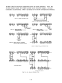
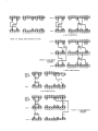
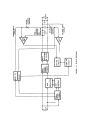


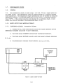


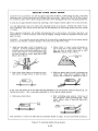


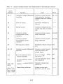

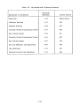
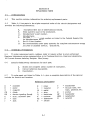


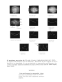
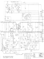


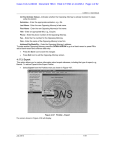


![10780-90006 - 10780A Laser Receiver for 5501A [Prefix 1948] (Mar](http://vs1.manualzilla.com/store/data/006009643_1-6e2f54ebb2199ef6df634558ba4c1bb6-150x150.png)