1
Application Note 120
March 2010
1ppm Settling Time Measurement
for a Monolithic 18-Bit DAC
When Does the Last Angel Stop Dancing on a Speeding Pinhead?
Jim Williams
Introduction
Performance requirements for instrumentation, function
generation, inertial navigation systems, trimming, calibrators, ATE, medical apparatus and other precision applications
are beginning to eclipse capabilities of 16-bit data converters. More specifically, 16-bit digital-to-analog converters
(DACs) have been unable to provide required resolution in
an increasing number of ultra-precision applications.
New components (see Components for 18-bit Digitalto-Analog Conversion, page 2) have made 18-bit DACs
a practical design alternative1. These ICs provide 18-bit
performance at reasonable cost compared to previous
modular and hybrid technologies. The monolithic DACs
DC and AC specifications approach or equal previous
converters at significantly lower cost.
DAC Settling Time
DAC DC specifications are relatively easy to verify. Measurement techniques are well understood, albeit often tedious.
AC specifications require more sophisticated approaches
to produce reliable information. In particular, the settling
time of a DAC and its output amplifier is extraordinarily
difficult to determine to 18-bit (4ppm) resolution. DAC settling time is the elapsed time from input code application
until the output arrives at, and remains within, a specified error band around the final value. To measure a new
18-bit DAC, a settling time measurement technique has
been developed with 20-bit (1ppm) resolution for times as
short as 265ns. The new method will work with any DAC.
Realizing this measurement capability and its performance
verification has required an unusually intense, extensive
and protracted effort. Hopefully, the data converter community will find the results useful2.
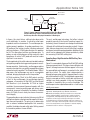
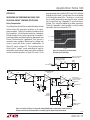
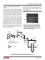
DAC settling time is usually specified for a full-scale 10V
transition. Figure 1 shows that DAC settling time has three
DAC INPUT
(ALL BITS)
SETTLING TIME
RING TIME
DAC OUTPUT
ALLOWABLE
OUTPUT
ERROR
BAND
SLEW
TIME
DELAY TIME
AN120 F01
Figure 1. DAC Settling Time Components Include Delay, Slew
and Ring Times. Fast Amplifiers Reduce Slew Time, Although
Longer Ring Time Usually Results. Delay Time is Normally a
Small Term
distinct components. The delay time is very small and is
almost entirely due to propagation delay through the DAC
and output amplifier. During this interval, there is no output
movement. During slew time, the output amplifier moves
at its highest possible speed towards the final value. Ring
time defines the region where the amplifier recovers from
slewing and ceases movement within some defined error
band. There is normally a trade-off between slew and ring
time. Fast slewing amplifiers generally have extended
ring times, complicating amplifier choice and frequency
L, LT, LTC and LTM are registered trademarks of Linear Technology Corporation.
All other trademarks are the property of their respective owners.
Note 1. See Appendix A, “A History of High Accuracy Digital-to-Analog
Conversion”.
Note 2. A historical note is in order. In early 1997, LTC’s DAC design
group tasked the author to measure 16-bit DAC settling time. The result
was published in July 1998 as Application Note 74, “Component and
Measurement Advances Ensure 16-Bit DAC Settling Time”. Almost
exactly 10 years later, the DAC group raised the ante, requesting 18-bit
DAC settling time measurement. This constitutes 2 bits of resolution
improvement per decade of author age. Since it was unclear how many
decades the author (born 1948) had left, it was decided to double jump
the performance requirement and attempt 20-bit resolution. In this way,
even if the author is unavailable in 10 years, the DAC group will still get its
remaining 2 bits.
an120f
AN120-1
Application Note 120
COMPONENTS FOR 18-BIT D/A CONVERSION
Components suitable for 18-bit D/A conversion are
members of an elite class. 18 binary bits is one part
in 262,144—just 0.0004% or 4 parts-per-million. This
mandates a vanishingly small error budget and the
demands on components are high. The LTC2757 digitalto-analog converter listed in the chart uses Si-Chrome
thin-film resistors for high stability and linearity over
temperature. Gain drift is typically 0.25ppm/°C or about
4.6LSBs over 0°C to 70°C. Some amplifiers shown
contribute less than 1LSB error over 0°C to 70°C with
18-bit DAC driven settling times of 1.8μs available. The
references offer drifts as low as 1LSB over 0°C to 70°C
with initial trimmed accuracy to 0.05%
Short Form Descriptions of Components Suitable for 18-Bit Digital-to-Analog Conversion
COMPONENT TYPE
ERROR CONTRIBUTION OVER 0°C TO 70°C
COMMENTS
LTC 2757 DAC
≈4.6LSB Gain Drift
1LSB Linearity
Full Parallel Inputs
Current Output
LT®1001 Amplifier
<1LSB
Good Low Speed Choice
10mA Output Capability
LT1012 Amplifier
<1LSB
Good Low Speed Choice
Low Power Consumption
LT1468/LT1468-2 Amplifier
<8LSB
1.8μs Settling to 18 Bits
Fastest Available
LTC1150 Amplifier
<1LSB
Lowest Error. ≈10ms Settling Time.
Requires LT1010 Output Buffer. Special
Case. See Appendix E
LTZ1000A Reference
<1LSB
Lowest Drift Reference in This Group.
4ppm (1LSB)/Yr. Time Stability Typical
LM199A Reference-6.95V
≈4LSB
Low Drift. 10ppm (2.5LSB) Yr. Time
Stability Typical
LT1021 Reference-10V
≈16LSB
Good General Purpose Choice
LT1027 Reference-5V
≈16LSB
Good General Purpose Choice
LT1236 Reference-10V
≈40LSB
Trimmed to 0.05% Absolute
Accuracy
®
compensation. Additionally, the architecture of very fast
amplifiers usually dictates trade-offs which degrade DC
error terms3.
Measuring anything at any speed to 20-bit resolution
(1ppm) is hard. Dynamic measurement to 20-bit resolution
is particularly challenging. Reliable 1ppm DAC settling time
measurement constitutes a high order difficulty problem
requiring exceptional care in approach and experimental
technique. This publication’s remaining sections describe
a method enabling an oscilloscope to accurately display
DAC settling time information for a 10V step with 1ppm
resolution (10μV) within 265ns. The approach employed
permits observation of small amplitude information at the
excursion limits of large waveforms without overdriving
the oscilloscope.
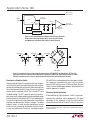
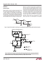
Considerations for Measuring DAC Settling Time
Historically, DAC settling time has been measured with
circuits similar to that in Figure 2. The circuit uses the
“false sum node” technique. The resistors and DAC form
a bridge type network. Assuming ideal components, the
DAC output will step to –VREF when the DAC inputs move
to all ones. During slew, the settle node is bounded by the
diodes, limiting voltage excursion. When settling occurs,
the oscilloscope probe voltage should be zero. Note that
the resistor divider’s attenuation means the probe’s output
will be one-half of the DAC’s settled voltage.
Note 3. This issue is treated in detail in latter portions of the text. Also see
Appendix D, “Practical Considerations for DAC-Amplifier Compensation”.
an120f
AN120-2
Application Note 120
INPUT STEP TO
OSCILLOSCOPE
DIGITAL
INPUT
0V TO 10V
TRANSITION
DAC
R
REF
SETTLE
NODE
OUTPUT TO
OSCILLOSCOPE
R
–10VREF
AN120 F02
Figure 2. Popular Summing Scheme for DAC Settling Time Measurement
Provides Misleading Results. 18-Bit Measurement Causes >800x
Oscilloscope Overdrive. Displayed Information is Meaningless
In theory, this circuit allows settling to be observed to
small amplitudes. In practice, it cannot be relied upon
to produce useful measurements. The oscilloscope connection presents problems. As probe capacitance rises,
AC loading of the resistor junction influences observed
settling waveforms. A 10pF probe alleviates this problem
but its 10x attenuation sacrifices oscilloscope gain. 1x
probes are not suitable because of their excessive input
capacitance. An active 1x FET probe will work, but a more
significant issue remains.
The clamp diodes at the settle node are intended to reduce
swing during amplifier slewing, preventing excessive oscilloscope overdrive. Unfortunately, oscilloscope overdrive
recovery characteristics vary widely among different types
and are not usually specified. The Schottky diodes’ 400mV
drop means the oscilloscope may see an unacceptable
overload, bringing displayed results into question4.
At 10-bit resolution (10mV at the DAC output, resulting
in 5mV at the oscilloscope), the oscilloscope typically
undergoes a 2x overdrive at 50mV/DIV, and the desired
5mV baseline is just discernible. At 12-bit or higher
resolution, the measurement becomes hopeless with this
arrangement. Increasing oscilloscope gain brings commensurate increased vulnerability to overdrive induced
errors. At 18 bits, there is clearly no chance of measurement integrity.
The preceding discussion indicates that measuring 18-bit
settling time requires a high gain oscilloscope that is somehow immune to overdrive. The gain issue is addressable
with an external wideband preamplifier that accurately
amplifies the diode-clamped settle node. Getting around
the overdrive problem is more difficult.
The only oscilloscope technology that offers inherent
overdrive immunity is the classical sampling ‘scope5. Unfortunately, these instruments are no longer manufactured
(although still available on the secondary market). It is possible, however, to construct a circuit that utilizes sampling
techniques to avoid the overload problem. Additionally, the
circuit can be endowed with features particularly suited
for measuring 20-bit DAC settling time.
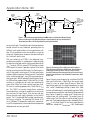
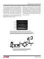
Sampling Based High Resolution DAC Settling Time
Measurement
Figure 3 is a conceptual diagram of the 20-bit DAC settling
time measurement circuit. This figure shares attributes with
Figure 2, although some new features appear. In this case,
the preamplified oscilloscope is connected to the settle
point by a switch. The switch state is determined by a
delayed pulse generator, which is triggered from the same
pulse that controls the DAC. The delayed pulse generator’s
timing is arranged so that the switch does not close until
settling is very nearly complete. In this way, the incoming
waveform is sampled in time, as well as amplitude. The
oscilloscope is never subjected to overdrive—no off-screen
activity ever occurs.
Note 4. For a discussion of oscilloscope overdrive considerations, see
Appendix B, “Evaluating Oscilloscope Overdrive Performance”.
Note 5. Classical sampling oscilloscopes should not be confused with
modern era digital sampling ‘scopes that have overdrive restrictions.
See Appendix B, “Evaluating Oscilloscope Overload Performance” for
comparisons of various type oscilloscopes with respect to overdrive.
For detailed discussion of classical sampling oscilloscope operation, see
references 17 through 21 and 23 through 25. Reference 18 is noteworthy;
it is the most clearly written, concise explanation of classical sampling
instruments the author is aware of. A 12-page jewel.
an120f
AN120-3
Application Note 120
INPUT STEP TO
OSCILLOSCOPE
DIGITAL
INPUT
0V TO 10V
TRANSITION
DAC
R
REF
SWITCH
OUTPUT TO
OSCILLOSCOPE
SETTLE
NODE
R
RESIDUE
AMPLIFIER
–10VREF
DELAYED
PULSE GENERATOR
AN120 F03
Figure 3. Conceptual Arrangement Eliminates Oscilloscope Overdrive.
Delayed Pulse Generator Controls Switch, Preventing Oscilloscope
from Monitoring Settle Node Until Settling is Nearly Complete
V+
SIGNAL PATH
SIGNAL PATH
SIGNAL PATH
CONTROL
JFET
MOSFET
AN120 F04
V–
DIODE BRIDGE
Figure 4. Conventional Choices for the Sampling Switch Include JFET, MOSFET and Diode Bridge. FET Parasitic
Capacitances Result in Large Gate Drive Originated Feedthrough to Signal Path. Diode Bridge is Better; Its Small
Parasitic Capacitances Tend to Cancel. Bridge Requires DC and AC Trims and Complex Drive Circuitry
Developing a Sampling Switch
Requirements for Figure 3’s sampling switch are stringent.
It must faithfully pass signal path information without introducing alien components, particularly those deriving from
the switch command channel. Figure 4 shows conventional
choices for the sampling switch. They include FETs and
the diode bridge. The FET’s parasitic gate to channel capacitances result in large gate drive originated feedthrough
into the signal path. For almost all FETs, this feedthrough is
many times larger than the signal to be observed, inducing
overload and obviating the switches’ purpose. The diode
bridge is better; its small parasitic capacitances tend to
cancel and the symmetrical, differential structure results
in very low feedthrough. Practically, the bridge requires
DC and AC trims and complex drive and support circuitry.
This approach, incarnated with great care, can reliably
measure DAC settling time to 16-bit resolution6. Beyond
16 bits, residual feedthrough becomes objectionable and
another approach is needed.
Electronic Switch Equivalents
A low feedthrough, high resolution “switch” can be constructed with wideband active components. The great
advantage of this approach is that the switch control
channel can be maintained “in-band”; that is, its transition
Note 6. LTC Application Note 74, “Component and Measurement Advances
Ensure 16-bit DAC Settling Time” utilized such a sampling bridge and it is
detailed in that text.
an120f
AN120-4
Application Note 120
rate is within the circuits’ bandpass. The circuit’s wide
bandwidth means the switch command transition is under
control at all times. There are no out-of-band responses,
greatly reducing feedthrough. Figure 5 lists some candidates for low feedthrough electronic switch equivalents.
A and B, while theoretically possible, are cumbersome to
implement. C and D are practical. C must be optimized for
low feedthrough on rising and falling control pulse edges
because of the multiplier’s unrestricted wideband response.
D’s falling edge feedthrough is inherently minimized by the
gm amplifiers transconductance collapse when the control
pulse goes low. This allows feedthrough to be optimized
for the control pulse’s rising edge without regard to falling
edge effects. This is a significant advantage in constructing
an electronic equivalent switch.
collapse on the falling edge ensures low feedthrough for
that condition, preventing oscilloscope overdrive. Figure 7
details the transconductance amplifier-based switch. This
design switches signals over a ±30mV range with peak
control channel feedthrough of millivolts and settling
times inside 40ns.
The circuit approximates switch action by varying A1A’s
transconductance; the maximum gain is unity. At low
transconductance, A1A’s gain is nearly zero, and essentially
no signal is passed. At maximum transconductance, signal
A = 0.001
SIGNAL
INPUT
SIGNAL
OUTPUT
gm
IIN
Transconductance Amplifier Based Switch Equivalent
Figure 6 is a conceptual transconductance amplifier based
“switch”. The wideband control and signal paths faithfully track 1000:1 transconductance change, resulting in
exceptionally pure switch dynamics. The switched current source is carefully optimized for lowest feedthrough
on the rising control edge without regard to falling edge
characteristics. The gm amplifier’s transconductance
1
SWITCHED CURRENT = 1000 • I
IDLE CURRENT = I
CURRENT ON
CURRENT OFF
CURRENT SOURCE
CONTROL CHANNEL
AN120 F06
Figure 6. Transconductance Amplifier Based “Switch” Has
Minimal Control Channel Feedthrough. Wideband Control and
Signal Paths Faithfully Track 1000:1 Transconductance Change,
Resulting in Exceptionally Pure Switch Dynamics
CONTROL PULSE (EDGES IN-BAND)
A
B
IN
IN
OUT
OUT
CONTROL PULSE (EDGES IN-BAND)
C
IN
1V
FULL-SCALE
X
X
Z
OUT
D
IN
gm
OUT
Y
AN120 F05
1V
0V
CONTROL PULSE
(EDGES IN-BAND)
CONTROL PULSE
(LEADING EDGE IN-BAND)
V–
Figure 5. Conceptual Low Feedthrough Electronic Switch Equivalents. A and B are Difficult to Implement,
C and D are Practical. C Must be Optimized for Low Feedthrough on Rising and Falling Control Pulse
Edges. D’s Falling Edge Feedthrough is Inherently Minimized by Attendant Bandwidth Reduction
an120f
AN120-5
Application Note 120
15V
5V
SWITCH
CONTROL
INPUT
200Ω 1N4148
0V
1.6k
7.5k*
SIGNAL
INPUT
0mV TO ±30mV
10k**
+
0.02μF
A1A
1/2 LT1228
Q1
2N3906
SAMPLE
TRANSITION
PURITY
3.57k*
50pF
15V
7.5k
1μF
15V
10Ω
–
5k
+
ISET
50Ω
50pF
ABERRATIONS
50Ω
GAIN
A1B
1/2 LT1228
–
1k
OUTPUT
0mV TO ±60mV
(0mV TO ±30mV)
WHEN DRIVING
50Ω BACKTERMINATED
CABLE)
–15V
–15V
ZERO
10M
*1% METAL FILM
**3300ppm/°C, 5%
QUALITY THERMISTOR,
#QTG12-103G
1k
AN120 F07
Figure 7. Transconductance Amplifier-Based 100MHz Low Level Switch Has Minimal Control
Channel Feedthrough. A1A’s Unity-Gain Output is Cleanly Switched by Logic Controlled Q1’s
Transconductance Bias. A1B Provides Buffering and Signal Path Gain
passes at unity gain. The amplifier and its transconductance
control channel are very wideband, permitting them to
faithfully track rapid variations in transconductance setting. This characteristic means the amplifier is never out
of control, affording clean response and rapid settling to
the “switched” input’s value.
A1A, one section of an LT1228, is the wideband transconductance amplifier. Its voltage gain is determined by
its output resistor load and the current magnitude into its
“ISET” terminal. A1B, the second LT1228 section, unloads
A1A’s output. As shown, it provides a gain of 2, but when
driving a back-terminated 50Ω cable, its effective gain is
unity at the cable’s receiving end. The back termination
enforces a 50Ω environment. Current source Q1, controlled
by the “switch control input”, sets A1A’s transconductance,
and, hence, gain. With Q1 gated off (control input at zero),
the 10M resistor supplies about 1.5μA into A1A’s ISET pin,
resulting in a voltage gain of nearly zero, blocking the
input signal. When the switch control input goes high,
Q1 turns on, sourcing approximately 1.5mA into the ISET
pin. This 1000:1 set current change forces maximum
transconductance, causing the amplifier to assume unity
gain and pass the input signal. Trims for zero and gain
ensure accurate input signal replication at the circuit’s
output. The Q1 associated 50pF variable capacitor purifies turn-on switching. The specified 10k resistor at Q1
has a 3300ppm/°C temperature coefficient, compensating A1A’s complementary transconductance temperature
dependence to minimize gain drift.
A = 5V/DIV
B = 0.01V/DIV
100ns/DIV
AN120 F08
Figure 8. Control Input (Trace A) Dictates Switch Output’s
(Trace B) Representation of 0.01V DC Input. Control Channel
Feedthrough, Evident at Switch Turn-On, Settles in 20ns.
Turn-Off Feedthrough is Undetectable Due to Deceased Signal
Channel Transconductance and Bandwidth. CABERRATION ≈ 35pF
for this Test
Figure 8 shows circuit response for a switched 10mV DC
input and CABERRATION = 35pF. When the control input
(trace A) is low, no output (trace B) occurs. When the
control input goes high, the output reproduces the input
with “switch” feedthrough settling in about 20ns. Note
that turn-off feedthrough is undetectable due to the 1000x
transconductance reduction and attendant 25x bandwidth
drop. Figure 9 speeds the sweep up to 10ns/division to
examine zero volt settling detail. The output (trace B)
settles inside 1mV 40ns after the switch control (trace A)
goes high. Peak feedthrough excursion, damped by CABERRATION, is only 5mV. Figure 10 was taken under identical
conditions, except that CABERRATION = 0pF. Feedthrough
an120f
AN120-6
Application Note 120
increases to approximately 20mV, although settling time
to 1mV remains at 40ns. Figure 11, using double exposure technique, compares signal channel rise times for
CABERRATION = 0pF (leftmost trace) and approximately 35pF
(rightmost trace) with the control channel tied high. The
larger CABERRATION value, while minimizing feedthrough
amplitude (see Figure 9), increases rise time by 7x versus
CABERRATION = 0pF.
A = 5V/DIV
B = 0.005V/DIV
10ns/DIV
AN120 F09
Figure 9. High Speed Delay and Feedthrough for 0V Signal
Input. Output (Trace B) Peaks Only 0.005V Before Settling
Inside 0.001V 40ns After Switch Control Command (Trace A).
CABERRATION ≈ 35pF for This Test
The transconductance switches’ small DC and AC errors
nicely accommodate the applications’ requirements. The
low feedthrough, already sufficient, becomes irrelevant
because its small time and amplitude error will be buried
in the DAC ring time interval. The transconductance amplifier based “switch” points the way towards practical 1ppm
DAC settling time measurement.
DAC Settling Time Measurement Method
A = 5V/DIV
B = 0.005V/DIV
10ns/DIV
AN120 F10
Figure 10. Identical Conditions as Figure 9 Except
CABERRATION = 0pF. Feedthrough Related Peaking Increases
to ≈0.02V; 0.001V Settling Time Remains at 40ns
Figure 12, a more complete representation of Figure 3,
utilizes the above described sampling switch. Figure 3’s
blocks appear in greater detail and some new refinements
show up. The DAC-amplifier summing area is unchanged.
Figure 3’s delayed pulse generator has been split into two
blocks; a delay and a pulse generator, both independently
variable. The input step to the oscilloscope runs through
a section that compensates settling time-measurement
path propagation delay. This path includes settle node,
amplifier and sample gate delays. The transconductance
sampling switch (“sample gate”), driven from a non-saturating residue amplifier, feeds the oscilloscope. Placing the
sampling switch after the residue amplifier gain further
minimizes sample command feedthrough impact.
Detailed Settling Time Circuitry
0.005V/DIV
10ns/DIV
AN120 F11
Figure 11. Signal Channel Rise Time for CABERRATION = 0pF
(Leftmost Trace) and ≈35pF (Rightmost Trace) Record 3.5ns
and 25ns, Respectively. Switch Control Input High for this
Measurement. Photograph Utilizes Double Exposure Technique
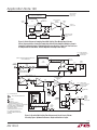
Figure 13 is a detailed schematic of the 20-bit DAC settling
time measurement circuitry. The input pulse switches all
DAC bits simultaneously and is also routed to the oscilloscope via the delay compensation network. The delay
network, composed of CMOS inverters and an adjustable
RC network, compensates the oscilloscope’s input step
signal for the 44ns delay through the circuit measurement
path7. The DAC-amplifier output is compared against the
Note 7. See Appendix C, “Measuring and Compensating Signal Path Delay
and Circuit Trimming Procedures”.
an120f
AN120-7
Application Note 120
TIME CORRECTED
INPUT STEP TO
OSCILLOSCOPE
SETTLE NODE-RESIDUE AMPLIFIER-SAMPLE
GATE DELAY COMPENSATION
DIGITAL
INPUT
0V TO 10V
TRANSITION
DAC
NON-SATURATING
RESIDUE
AMPLIFIER
R
REF
SAMPLE
GATE
OUTPUT TO
OSCILLOSCOPE
SETTLE
NODE
IIN
R
–10VREF
SAMPLE WINDOW
GENERATOR
VARIABLE
DELAY
VARIABLE WIDTH
PULSE GENERATOR
TRANSCONDUCTANCE
CONTROL CURRENT
SOURCE
SAMPLE COMMAND PULSE
AN120 F03
Figure 12. Block Diagram of Sampling-Based DAC Settling Time Measurement Scheme.
Placing Transconductance Controlled Sample Gate After Residue Amplifier Minimizes Sample
Command Feedthrough Impact, Eliminating Oscilloscope Overdrive. Input Step Time Reference
is Compensated for Settle Node, Residue Amplifier and Sample Gate Delays
4.99k* TIME CORRECTED
INPUT STEP TO 50Ω
OSCILLOSCOPE
5V
SETTLE NODE-RESIDUE AMPLIFIER-SAMPLE GATE
DELAY COMPENSATION
PULSE
GENERATOR
INPUT
FB
1k
DELAY
COMP
5V
CCOMP TYPICAL 22pF
(SELECT—SEE TEXT)
DUT
LTC2757
0V TO 10V
TRANSITION
15V
–
+
REF
10k***
LT1021-10
IN
OUT
GND
–15V NC
75pF
tD = 44ns
0.1μF
+
50Ω
IN-LINE TERMINATION
(SEE TEXT AND NOTES)
SETTLE
NODE
10k***
AUT
LT1468
–10VREF
47μF 500Ω
TANT
–15V
+
A1
RESIDUE AMPLIFIER, A = 40
750Ω
–
A2
+
LT1221
VARIABLE
TRANSCONDUCTANCE
AMPLIFIER
180Ω
–
A3
+
LT1221
3.01k*
CFA
1/2 LT1228
ISET
3.01k*
–
560Ω*
5V
: 1N4148
5k
–
VCC RC1
A1
B1
C1
CLR1
5V
Q1 Q2 CLR2
74HC123
Q1 Q2 C2
1μF
10k**
A2
7.5k*
1.6k
2N3906
3.57k*
RC2 GND
470pF
1k
SETTLE OUTPUT
TO 50Ω OSCILLOSCOPE.
1mV/DIV = 50μV/DIV
AT DAC OUTPUT
5V
20k
SAMPLE
DELAY
–5V
15V
SAMPLE
WINDOW
GENERATOR
B2
1k*
100k
1k*
0.02μF
*1% METAL FILM RESISTOR
**QUALITY THERMISTOR, #QTG12-103G
***VISHAY S102, 0.01% RESISTOR: 10pmm MATCHING
USE IN-LINE COAXIAL 50Ω TERMINATOR FOR
PULSE GENERATOR INPUT. DO NOT MOUNT
50Ω RESISTOR ON BOARD
CONSTRUCTION IS CRITICAL—SEE TEXT
DAC CONNECTIONS SIMPLIFIED FOR
SCHEMATIC CLARITY. SEE THE LTC2757
DATA SHEET
50Ω*
1k BASELINE ZERO
100Ω
5V
: 1N5712
A4
1/2 LT1228
ABERRATIONS
SAMPLE
INTERVAL
ZERO
SAMPLE
WINDOW
WIDTH
100pF
5k
50pF
10k
1k
–5V
: 74HC04, GROUND UNUSED INPUTS
50Ω
50Ω
GAIN
560Ω*
5V
ICs = ±15V UNLESS NOTED
+
200Ω
50pF
SAMPLE
TRANSITION
PURITY
4.99k*
SAMPLE
WINDOW
OUTPUT
TO 50Ω
OSCILLOSCOPE
SAMPLE
COMMAND
10M
5V
AN120 F13
Figure 13. Detailed DAC Settling Time Measurement Circuit Closely Follows
Preceding Figure. Optimum Performance Requires Attention to Layout
an120f
AN120-8
Application Note 120
LT1021 10V reference via the precision 10k summing
resistors. The LT1021 also furnishes the DAC reference,
making the measurement ratiometric. The clamped settle
node is unloaded by A1, which takes gain. A2 provides
additional clamped gain for a total summing node referred
amplification of 40. A2’s output feeds the sampling switch
whose operation is identical to Figure 7’s description.
The A1-A2 amplifier’s clamping and gain are arranged so
saturation never occurs—the amplifier is always in its
active region.
The input pulse triggers the 74HC123 dual one shot. The
one shot is arranged to produce a delayed (controllable by
the 20k potentiometer) pulse whose width (controllable by
the 5k potentiometer) sets sampling switch on-time. If the
delay is set appropriately, the oscilloscope will not see any
input until settling is nearly complete, eliminating overdrive.
The sample window width is adjusted so that all remaining
activity is observable. In this way, the oscilloscope output
is reliable and meaningful data may be taken.
Figure 14 shows circuit waveforms. Trace A is the time
corrected input pulse, trace B the sample gate, trace C the
DAC-amplifier output and trace D the circuit output. When
the sample gate goes high, trace D’s switching is clean,
the last millivolt of ring time is easily observed and the
amplifier settles nicely to final value bounded by broadband
noise. When the sample gate goes low, the transconductance switch goes off and no feedthrough is discernible.
Note that there is no off-screen activity at any time—the
oscilloscope is never subjected to overdrive.
The circuit requires trimming to achieve this level of
performance8. Figure 15 shows a typical display resulting from poor “Sample Interval Zero” adjustment. This
adjustment, corrected in Figure 16, results in a continuous
baseline. Sample command feedthrough is just visible at
trace B’s leading edge. Figure 17 shows output response
(trace B) to the sample command (trace A) turn-on before
trimming “aberrations” and “transition purity”9. Delay is
approximately 20ns with aberrations peaking 350μV and
Note 8. To maintain text flow and focus, trimming procedures are not
presented here. Detailed trimming information appears in Appendix C.
Note 9. A1’s positive input was grounded via 5kΩ (precision 10k resistors
disconnected) for Figure 17 and 18’s tests.
A = 5V/DIV
B = 10mV/DIV
(250μV/DIV WITH
RESPECT TO A1)
1μs/DIV
AN120 F15
Figure 15. Poor Sample Interval Zero Adjustment Causes Shifted
Output Baseline (Trace B) During Trace A’s Sample Interval
A = 5V/DIV
B = 10mV/DIV
(250μV/DIV WITH
RESPECT TO A1)
1μs/DIV
AN120 F16
Figure 16. Trimmed Sample Interval Zero Has No Output
Baseline Deviation (Trace B) During Sample Interval
(Trace A). Sample Command Feedthrough is Just
Visible at Trace B’s Leading Edge
A = 10V/DIV
B = 10V/DIV
A = 5V/DIV
B = 10mV/DIV
(250μV/DIV WITH
RESPECT TO A1)
C = 10V/DIV
D = 500μV/DIV
1μs/DIV
AN120 F14
Figure 14. Settling Time Circuit Waveforms Include Time
Corrected Input Pulse (Trace A), Sample Command (Trace B),
DAC Output (Trace C) and Settling Time Output (Trace D).
Sample Window Delay and Width are Variable
50ns/DIV
AN120 F17
Figure 17. Output Response (Trace B) To Sample Command
(Trace A) Turn-On Before Trimming Aberrations and Transition
Purity. Delay is ≈20ns. Aberrations Peak 350μV, Settle in
50ns. A1’s Positive Input Grounded via 5kΩ for This and
Succeeding Figures
an120f
AN120-9
Application Note 120
Circuit gain is adjusted with the indicated potentiometer.
1
(20)
RESOLUTION IN PPM (BITS)
settling in 50ns. Figure 18 shows post trim response to
sample command turn-on. Delay increases to 70ns but
aberrations peak only 50μV, settling in 50ns. Figure 19
shows output response (trace B) to sample command
(trace A) turn-off. The 1000:1 transconductance drop
ensures a clean transition independent of the turn-on
optimized trims.
4 SAMPLE COMMAND
PATH DELAYS
(18)
SAMPLING GATE
SETTLING TIME
16
(16)
64
(14)
256
(12) 0
40 80 120 160 200 240 280
MINIMUM MEASUREABLE SETTLING TIME (ns)
AN120 F20
A = 5V/DIV
Figure 20. Minimum Measureable Settling Time vs Resolution.
Limits are Imposed by Sample Command Path Delays and
Sample Gate Settling Profile. Resolution Beyond ≈15ppm
Requires Filtering or Noise Averaging
B = 10mV/DIV
(250μV/DIV WITH
RESPECT TO A1)
50ns/DIV
AN120 F18
Figure 18. Post-Trim Output Response (Trace B) To Sample
Command Turn-On, Trace A. Delay Increases to 70ns but
Aberrations Peak Only 50μV, Settling in 50ns
A = 5V/DIV
B = 10mV/DIV
(250μV/DIV WITH
RESPECT TO A1)
50ns/DIV
AN120 F19
Figure 19. Output Response (Trace B) To Sample Command
(Trace A) Turn-Off. 1000:1 Transconductance Drop Ensures
Clean Transition, Independent of Trim State
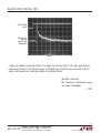
Settling Time Circuit Performance
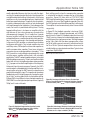
Figure 20 summarizes settling time circuit performance.
The graph indicates the minimum measurable settling time
for a given resolution. Speed limitations are imposed by
sample command path delays and sample gate switching residue profile10. Minimum measurable settling time
below 160ns is available to 16-bit resolution. Beyond this
point, the sample gate’s switching residue profile dictates
increased minimum measurable settling time to about
265ns at 20 bits. Circuit noise limitations are imposed by
the DAC/amplifier, summing resistors, and residue amplifier/sampling switch with about equal weighting. Because
of this, resolution beyond approximately 15ppm requires
filtering or noise averaging techniques.
Using the Sampling-Based Settling Time Circuit
It is good practice to “walk” the sampling window backwards
in time from the settled region up to the last 100μV or so of
amplifier movement so ring time cessation is observable.
The sampling-based approach provides this capability and
it is a very powerful measurement tool. Additionally, slower
amplifiers may require extended delay and/or sampling
window times. This may necessitate larger capacitor values
in the 74HC123 one-shot timing networks.
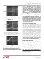
Figure 21 shows DAC settling in an unfiltered bandpass.
The DAC settles (trace B) to 16 bits 1.7μs after trace A’s
time corrected input step11. Sample gate feedthrough is
undetectable, indicating higher resolution is possible without overdriving the oscilloscope. Noise is the fundamental
measurement limit. Figure 22 attenuates noise by reducing
measurement bandwidth to 250kHz. Trace assignments are
as in the previous photo. 18-bit settling (4ppm) requires
approximately 5μs. The reduced bandwidth permits higher
resolution although the indicated settling time is likely
pessimistic due to the filter’s lag. Figure 23, decreasing
bandwidth to 50kHz, permits 19-bit (2ppm) resolution with
indicated settling in about 9μs. Again, the same filtering
which permits high resolution almost certainly lengthens
observed settling time.
Note 10. Driving the sample command path (74HC123 B2 input) with a
phase-advanced version of the pulse generator input largely eliminates
sample command path delay induced error, considerably improving
minimum measurable settling time. This benefit is not germane to the
present efforts purposes and was not implemented
Note 11. Settling time is significantly affected by the DAC-amplifier
compensation capacitor. See Appendix D, “Practical Considerations for
DAC-amplifier Compensation” for tutorial.
an120f
AN120-10
Application Note 120
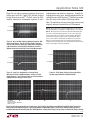
Figure 24 uses noise averaging techniques to measure
settling time to 20 bits (1ppm-10μV) without the band
limiting filter’s time penalty12. Photo A shows the DACamplifier adjusted for overdamped response, B and C
underdamped and optimum responses, respectively.
Averaging eliminates noise, permitting determination of
settling time due to DAC dynamics13. Settling time ranges
from 4μs to 6μs with fractional LSB tailing evident.
Note: This application note was derived from a manuscript
originally prepared for publication in EDN magazine.
A = 5V/DIV
Note 12. Most oscilloscopes require preamplification to resolve Figure
24’s signal amplitudes. See Appendix I, “Auxiliary Circuits” for an example.
Note 13. More properly, this measurement determines DAC settling time
due solely to step input initiated dynamics. For this reason, Figure 24’s
averaged results may be considered somewhat academic. Noise limits
measurement certainty at any given instant to approximately 100μV.
It is not unreasonable to maintain that this 100μV of noise means the
DAC never settles inside this limit. The averaged measurement defines
settling time with noise limitations removed. Hopefully, this disclosure will
appease technolawyers among the readership.
B = 500μV/DIV
1μs/DIV
AN120 F21
Figure 21. 0V to 10V DAC Settling in Unfiltered Bandpass. DAC
Settles (Settle Output, Trace B) to 16 Bits (15ppm) <2μs After
Trace A’s Time Corrected Input Step. Sample Gate Feedthrough
is Well Controlled, Indicating Higher Resolution is Possible
Without Overdriving Oscilloscope. Noise Limits Measurement
A = 5V/DIV
A = 5V/DIV
B = 100μV/DIV
B = 250μV/DIV
1μs/DIV
AN120 F22
Figure 23. 19 Bit (2ppm) Settling is Discernable About
9μs After Input Command in 50kHz Bandwidth
Figure 22. Same Trace Assignments as Previous Photo;
Measurement Taken in 250kHz Bandpass. Settling to 18 Bits
(4ppm) Requires ≈ 5μs. Filtering Permits Increased Resolution
Although Indicated Settling Time Increases
ALL PHOTOS
A
TRACE A = 5V/DIV
TRACE B = 25μV/DIV (AVERAGED)
HORIZ = 1μs/DIV
AN120 F23
2μs/DIV
AN120 F24
B
C
Figure 24. Noise Averaging Oscilloscope Permits 1ppm, (10μV) Settling Time Measurement Without Bandlimiting Filter Time Penalty.
Photo A Shows Overdamped Response, B and C Underdamped and Optimum Responses, Respectively. Averaging Eliminates Noise,
Permitting Determination of Settling Time Due To DAC Dynamics. Settling Times Range From 4μs to 6μs; Fractional LSB Tailing is Evident
an120f
AN120-11
Application Note 120
REFERENCES
1. Williams, Jim, “Component and Measurement Advances
Ensure 16-Bit DAC Settling Time,” Linear Technology
Corporation, Application Note 74, July 1998.
2. Williams, Jim, “Measuring 16-Bit Settling Times: The
Art of Timely Accuracy,” EDN, November 19, 1998.
3. Williams, Jim, “Methods for Measuring Op Amp Settling Time,” Linear Technology Corporation, Application
Note 10, July 1985.
4. Demerow, R., “Settling Time of Operational Amplifiers,” Analog Dialogue, Volume 4-1, Analog Devices,
Inc., 1970.
5. Pease, R.A., “The Subtleties of Settling Time,” The New
Lightning Empiricist, Teledyne Philbrick, June 1971.
6. Harvey, Barry, “Take the Guesswork Out of Settling Time
Measurements,” EDN, September 19, 1985.
7. Williams, Jim, “Settling Time Measurement Demands
Precise Test Circuitry,” EDN, November 15, 1984.
8. Schoenwetter, H.R., “High-Accuracy Settling Time
Measurements,” IEEE Transactions on Instrumentation
and Measurement, Vol. IM-32, No.1, March 1983.
9. Sheingold, D.H., “DAC Settling Time Measurement,”
Analog-Digital Conversion Handbook, pg. 312-317. Prentice-Hall, 1986.
16. Korn, G.A. and Korn, T.M., “Electronic Analog and
Hybrid Computers,” “Diode Switches,” pg. 223-226.
McGraw-Hill, 1964.
17. Carlson, R., “A Versatile New DC-500 MHz Oscilloscope with High Sensitivity and Dual Channel Display,”
Hewlett-Packard Journal, Hewlett-Packard Company,
January 1960.
18. Tektronix, Inc., “Sampling Notes,” Tektronix, Inc.,
1964.
19. Tektronix, Inc., “Type 1S1 Sampling Plug-In Operating
and Service Manual,” Tektronix, Inc., 1965.
20. Mulvey, J., “Sampling Oscilloscope Circuits,” Tektronix,
Inc., Concept Series, 1970.
21. Addis, John, “Sampling Oscilloscopes,” Private Communication, February 1991.
22. Williams, Jim, “Bridge Circuits-Marrying Gain and
Balance,” Linear Technology Corporation, Application
Note 43, June 1990.
23. Tektronix, Inc., “Type 661 Sampling Oscilloscope
Operating and Service Manual,” Tektronix, Inc., 1963.
24. Tektronix, Inc., “Type 4S1 Sampling Plug-In Operating
and Service Manual,” Tektronix, Inc., 1963.
25. Tektronix, Inc., “Type 5T3 Timing Unit Operating and
Service Manual,” Tektronix, Inc., 1965.
10. Williams, Jim, “30 Nanosecond Settling Time Measurement for a Precision Wideband Amplifier,” Linear Technology Corporation, Application Note 79, September 1999.
26. Morrison, Ralph, “Grounding and Shielding Techniques
in Instrumentation,” 2nd Edition, Wiley Interscience,
1977.
11. Williams, Jim, “Evaluating Oscilloscope Overload
Performance,” Box Section A, in “Methods for Measuring
Op Amp Settling Time,” Linear Technology Corporation,
Application Note 10, July 1985.
27. Ott, Henry W., “Noise Reduction Techniques in Electronic Systems,” Wiley Interscience, 1976.
28. Williams, Jim, “High Speed Amplifier Techniques,” Linear Technology Corporation, Application Note 47, 1991.
12. Orwiler, Bob, “Oscilloscope Vertical Amplifiers,” Tektronix, Inc., Concept Series, 1969.
29. Tektronix, Inc., “Type 109 Pulse Generator Operating
and Service Manual,” Tektronix, Inc., 1963.
13. Addis, John, “Fast Vertical Amplifiers and Good
Engineering,” “Analog Circuit Design; Art, Science and
Personalities,” Butterworth-Heinemann, 1991.
14. Travis, W., “Settling Time Measurement Using Delayed
Switch,” Private Communication, 1984.
30. Williams, Jim, “Signal Sources, Conditioners and
Power Circuitry,” “Wideband, Low Feedthrough, Low Level
Switch”, pg. 13-15. Appendix A, “How Much Bandwidth
is Enough?”, pg. 26, Linear Technology Corporation, Application Note 98, November 2004.
15. Hewlett-Packard, “Schottky Diodes for High-Volume,
Low Cost Applications,” Application Note 942, HewlettPackard Company, 1973.
31. Williams, Jim, “Applications Considerations and Circuits
for a New Chopper-Stabilized Op Amp,” Linear Technology
Corporation, Application Note 9, March 1985.
an120f
AN120-12
Application Note 120
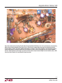
APPENDIX A
A HISTORY OF HIGH ACCURACY
DIGITAL-TO-ANALOG CONVERSION
People have been converting digital-to-analog quantities
for a long time. Probably among the earliest uses was the
summing of calibrated weights (Figure A1, left) in weighing
applications. Early electrical digital-to-analog conversion
inevitably involved switches and resistors of different
values, usually arranged in decades. The application was
often the calibrated balancing of a bridge or reading, via
null detection, some unknown voltage. The most accurate
resistor-based DAC of this type is Lord Kelvin’s Kelvin-Varley divider (Figure, large box). Based on switched resistor
ratios, it can achieve ratio accuracies of 0.1ppm (23+ bits)
and is still widely employed in standards laboratories. High
speed digital-to-analog conversion resorts to electronically
switching the resistor network. Early electronic DACs were
built at the board level using discrete precision resistors
and Germanium transistors (Figure, center foreground,
is a 12-bit DAC from a Minuteman missile D-17B inertial
navigation system, circa 1962). The first electronically
switched DACs available as standard product were probably those produced by Pastoriza Electronics in the mid
1960s. Other manufacturers followed and discrete-and
monolithically-based modular DACs (Figure, right and left)
became popular by the 1970s. The units were often potted
(Figure, left) for ruggedness, performance or to (hopefully)
preserve proprietary knowledge. Hybrid technology produced smaller package size (Figure, left foreground). The
development of Si-Chrome resistors permitted precision
monolithic DACs such as the LTC2757 (Figure, immediate
foreground). In keeping with all things monolithic, the
cost-performance trade-off of modern high resolution
IC DACs is a bargain. Think of it! An 18-bit DAC in an IC
package. What Lord Kelvin would have given for a credit
card and LTC’s phone number.
Figure A1. Historically Significant Digital-to-Analog Converters Include: Weight Set (Center Left), 23+ Bit Kelvin-Varley Divider
(Large Box), Hybrid, Board and Modular Types, and the LTC2757 IC (Foreground). Where Will It All End?
an120f
AN120-13
Application Note 120
APPENDIX B
EVALUATING OSCILLOSCOPE OVERDRIVE
PERFORMANCE
The settling-time circuit is heavily oriented towards
eliminating overdrive at the monitoring oscilloscope.
Oscilloscope recovery from overdrive is a murky area
and almost never specified. How long must one wait after
an overdrive before the display can be taken seriously?
The answer to this question is quite complex. Factors
involved include the degree of overdrive, its duty cycle,
its magnitude in time and amplitude and other considerations. Oscilloscope response to overdrive varies widely
between types and markedly different behavior can be
observed in any individual instrument. For example, the
recovery time for a 100x overload at 0.005V/DIV may be
very different than at 0.1V/DIV. The recovery characteristic may also vary with waveform shape, DC content and
repetition rate. With so many variables, it is clear that
measurements involving oscilloscope overdrive must be
approached with caution.
Why do most oscilloscopes have so much trouble recovering from overdrive? The answer to this question requires
some study of the three basic oscilloscope types’ vertical
paths. The types include analog (Figure B1A), digital (Figure
B1B) and classical sampling (Figure B1C) oscilloscopes.
Analog and digital ‘scopes are susceptible to overdrive.
The classical sampling ‘scope is the only architecture that
is inherently immune to overdrive.
An analog oscilloscope (Figure B1A) is a real-time, continuous linear system1. The input is applied to an attenuator,
which is unloaded by a wideband buffer. The vertical preamp
provides gain, and drives the trigger pick-off, delay line
and the vertical output amplifier. The attenuator and delay
line are passive elements and require little comment. The
buffer, preamp and vertical output amplifier are complex
linear gain blocks, each with dynamic operating range
restrictions. Additionally, the operating point of each block
may be set by inherent circuit balance, low frequency
stabilization paths or both. When the input is overdriven,
one or more of these stages may saturate, forcing internal
nodes and components to abnormal operating points and
temperatures. When the overload ceases, full recovery
of the electronic and thermal time constants may require
surprising lengths of time2.
The digital sampling oscilloscope (Figure B1B) eliminates
the vertical output amplifier, but has an attenuator buffer and
amplifiers ahead of the A/D converter. Because of this, it is
similarly susceptible to overdrive recovery problems.
The classical sampling oscilloscope is unique. Its nature
of operation makes it inherently immune to overload.
Figure B1C shows why. The sampling occurs before any
gain is taken in the system. Unlike Figure B1B’s digitally
sampled ‘scope, the input is fully passive to the sampling
point. Additionally, the output is fed back to the sampling
bridge, maintaining its operating point over a very wide
range of inputs. The dynamic swing available to maintain
the bridge output is large and easily accommodates a wide
range of oscilloscope inputs. Because of all this, the amplifiers in this instrument do not see overload, even at 1000x
overdrives, and there is no recovery problem. Additional
immunity derives from the instrument’s relatively slow
sample rate—even if the amplifiers were overloaded, they
would have plenty of time to recover between samples3.
The designers of classical sampling ‘scopes capitalized
on the overdrive immunity by including variable DC offset
generators to bias the feedback loop (see Figure B1C, lower
right). This permits the user to offset a large input, so small
amplitude activity on top of the signal can be accurately
observed. This is ideal for, among other things, settling
time measurements. Unfortunately, classical sampling
oscilloscopes are no longer manufactured, so if you have
one, take care of it!
Although analog and digital oscilloscopes are susceptible
to overdrive, many types can tolerate some degree of this
abuse. The early portion of this Appendix stressed that
measurements involving oscilloscope overdrive must
be approached with caution. Nevertheless, a simple test
can indicate when the oscilloscope is being deleteriously
affected by overdrive.
Note 1: Ergo, the Real Thing. Hopelessly bigoted residents of this locale
mourn the passing of the analog ‘scope era and frantically hoard every
instrument they can find.
Note 2: Some discussion of input overdrive effects in analog oscilloscope
circuitry is found in reference 13.
Note 3: Additional information and detailed treatment of classical sampling
oscilloscope operation appears in references 17-20 and 23-25.
an120f
AN120-14
Application Note 120
INPUT
ATTENUATOR
ATTENUATOR
BUFFER
V+
A
ANALOG
OSCILLOSCOPE
VERTICAL
CHANNEL
TRIGGER
CIRCUITRY
TO HORIZONTAL/
SWEEP SECTION
DELAY LINE
TO CRT
VERTICAL
PREAMP
VERTICAL
OUTPUT
V–
INPUT
ATTENUATOR
ATTENUATOR
BUFFER
V+
TRIGGER
CIRCUITRY
A/D CONTROL
TIMING
GENERATOR
SAMPLE
COMMAND
B
DIGITAL
SAMPLING
OSCILLOSCOPE
VERTICAL
CHANNEL
A/D
VERTICAL
PREAMP
MEMORY
A/D DRIVER
AMP
MICROPROCESSOR
TO CRT
V–
V+ V–
PULSE STRETCHER—
MEMORY SWITCH
DRIVER
MEMORY
INPUT
C
CLASSICAL
SAMPLING
OSCILLOSCOPE
VERTICAL
CHANNEL
DELAY LINE
TO CRT
AC
AMPLIFIER
FEEDBACK
VERTICAL
AMPLIFIER
V – V+
DC OFFSET
GENERATOR
TRIGGER
CIRCUITRY
TO HORIZONTAL CIRCUITS
AN120 FB1
Figure B1. Simplified Vertical Channel Diagrams for Different Type Oscilloscopes. Only the Classical Sampling Scope
(C) Has Inherent Overdrive Immunity. Offset Generator Allows Viewing Small Signals Riding on Large Excursions
an120f
AN120-15
Application Note 120
The waveform to be expanded is placed on the screen at
a vertical sensitivity that eliminates all off-screen activity.
Figure B2 shows the display. The lower right hand portion
is to be expanded. Increasing the vertical sensitivity by a
factor of two (Figure B3) drives the waveform off-screen,
but the remaining display appears reasonable. Amplitude
has doubled and waveshape is consistent with the original
display. Looking carefully, it is possible to see small amplitude information presented as a dip in the waveform at
about the third vertical division. Some small disturbances
are also visible. This observed expansion of the original
waveform is believable. In Figure B4, gain has been further
increased, and all the features of Figure B3 are amplified
accordingly. The basic waveshape appears clearer and
the dip and small disturbances are also easier to see. No
new waveform characteristics are observed. Figure B5
brings some unpleasant surprises. This increase in gain
causes definite distortion. The initial negative-going peak,
although larger, has a different shape. Its bottom appears
1V/DIV
less broad than in Figure B4. Additionally, the peak’s positive recovery is shaped slightly differently. A new rippling
disturbance is visible in the center of the screen. This
kind of change indicates that the oscilloscope is having
trouble. A further test can confirm that this waveform is
being influenced by overloading. In Figure B6, gain remains
the same but the vertical position knob has been used to
reposition the display at the screen’s bottom.4 This shifts
the oscilloscope’s DC operating point which, under normal
circumstances, should not affect the displayed waveform.
Instead, a marked shift in waveform amplitude and outline
occurs. Repositioning the waveform to the screen’s top
produces a differently distorted waveform (Figure B7).
It is obvious that for this particular waveform, accurate
results cannot be obtained at this gain.
Note 4: Knobs (derived from Middle English, “knobbe”, akin to Middle Low
German, “knubbe”), cylindrically shaped, finger rotatable panel controls
for controlling instrument functions, were utilized by the ancients.
0.5V/DIV
0.2V/DIV
100ns/DIV
100ns/DIV
100ns/DIV
Figure B2
Figure B3
Figure B4
0.1V/DIV
0.1V/DIV
0.1V/DIV
100ns/DIV
100ns/DIV
100ns/DIV
Figure B5
Figure B6
Figure B7
AN120 FB2-B7
Figures B2-B7. The Overdrive Limit is Determined by Progressively
Increasing Oscilloscope Gain and Watching for Waveform Aberrations
an120f
AN120-16
Application Note 120
APPENDIX C
pulse-generator input at 200μV/DIV (note 10k-1Ω divider
feeding the settle node). Trace B shows the circuit output
at A4, delayed by about 44ns. This delay is a small error,
but is readily corrected by adjusting the delay network
for the same time lag. If appendix F’s serial interface is
utilized, 10ns should be added to the delay correction.
Similarly, if appendix I’s post amplifier is used, the delay
correction must be increased by 17ns.
MEASURING AND COMPENSATING SIGNAL PATH
DELAY AND CIRCUIT TRIMMING PROCEDURES
Delay Compensation
The settling time circuit utilizes an adjustable delay network
to time correct the input pulse for delays in the signalprocessing path. Typically, these delays introduce errors
of a few percent, so a first-order correction is adequate.
Setting the delay trim involves observing the network’s
input-output delay and adjusting for the appropriate time
interval. Determining the “appropriate” time interval is
somewhat more complex. Measuring the settling time
circuit’s signal path delay involves modifications to
Figure 13, shown in Figure C1. These changes lock the
circuit into its “sample” mode, permitting an input-tooutput delay measurement under signal-level conditions
similar to normal operation. In Figure C2, trace A is the
A = 200μV/DIV
B = 10mV/DIV
AN120 FC02
20ns/DIV
Figure C2. Sampling Circuit Input-Output
Delay Measures About 44ns
INPUT STEP REFERENCE
TO OSCILLOSCOPE
CONNECT SETTLE NODE
RESISTORS AS SHOWN
SETTLE
NODE
10k
10k
5V
PULSE INPUT
10k
1Ω
+
A1
RESIDUE AMPLIFIER, A = 40
750Ω
LT1221
–
+
VARIABLE
TRANSCONDUCTANCE
AMPLIFIER
A2
180Ω
–
A3
+
LT1221
3.01k
CFA
1/2 LT1228
ISET
3.01k
–
560Ω
50Ω
50pF
1k
A4
SETTLE OUTPUT
TO 50Ω OSCILLOSCOPE.
1mV/DIV = 50μV/DIV
AT DAC OUTPUT
5V
50Ω
1/2 LT1228
–
50Ω
GAIN
560Ω
5V
–5V
+
1k
100k
1k BASELINE ZERO
10k
ABERRATIONS
100Ω
1μF
–5V
1k
15V
SAMPLE
INTERVAL
ZERO
10k
SAMPLE
WINDOW
GENERATOR
7.5k
1.6k
2N3906
0.02μF
3.57k
200Ω
50pF
SAMPLE
TRANSITION
PURITY
SAMPLE
COMMAND
10M
DISCONNECT SAMPLE
COMMAND LINE
AN120 FC01
Figure C1. Partial Text Figure 13 Schematic Shows Modifications for Measuring Signal Path Delay.
Changes Lock Circuit into Sample Mode, Permitting Input-to-Output Delay Measurement
an120f
AN120-17
Application Note 120
Circuit Trimming Procedure
The following procedure, given in numerical order, trims
the settling time circuit for optimum performance. It is
advisable to execute trimming in the order given, avoiding
out-of-sequence adjustments.
1. Turn off input pulses.
2. Trim “Baseline Zero” for 0V out at oscilloscope at
10mV per division or less.
3. Disconnect precision 10k resistors and ground settle
node via 5.1kΩ.
4. Set sample delay to mid-range, sample window width
to minimum.
10. Turn off input pulses. Disconnect the pulse generator
and its 50Ω termination. Apply 5V DC to the pulse
input.
11. Connect Figure C3’s network to the settle node. The
added components shown furnish a 250μV DC gain
calibration source when the input pulses are replaced
by a 5V level. Under the figure’s conditions, the DAC
assumes a 10V output with the 5.1k resistor mimicking
the 10kΩ divider output impedance at A1. Figure 13’s
“Gain” trim is adjusted for a 10mV DC deflection at the
oscilloscope. This completes the trimming procedure
and the circuit is ready for use.
Note 1. The “Sample Interval Zero” trim is unnecessary if Appendix I’s
optional auto-zero circuitry is used.
5. Drive pulse generator input with 40kHz square
wave.
6. Adjust “Sample Interval Zero” for no offset between
the sample interval and the unsampled baseline1.
7. Adjust “Sample Transition Purity” and “Aberration”
trims for minimum amplitude disturbances when the
sample gate opens with oscilloscope horizontal at
50ns per division and vertical sensitivity of 10mV per
division.
8. Reconnect precision 10k resistors and remove 5.1kΩ
unit from the settle node.
9. Adjust “Delay Compensation” for 44ns delay from the
pulse generator input to the time corrected output
pulse.
PARTIAL FIGURE 13
DAC
10k
ADD THESE
COMPONENTS
5.1k
10k
0.25Ω
1%
–10V
REFERENCE
LT1021
TO A1
POSITIVE
INPUT
AN120 FC03
DISCONNECT
Figure C3. Added Components Furnish 250μV Gain Calibration
Source with Input Pulses Replaced by 5V Level. DAC Output
Assumes 10V Reference Potential Under These Conditions; 5.1k
Resistor Mimics 10kΩ Divider Output Impedance at A1
APPENDIX D
PRACTICAL CONSIDERATIONS FOR DAC-AMPLIFIER
COMPENSATION
There are a number of practical considerations in compensating the DAC-amplifier pair to get fastest settling time.
Our study begins by revisiting text Figure 1 (repeated here
as Figure D1). Settling time components include delay, slew
and ring times. Delay is due to propagation time through
the DAC-amplifier and is a very small term. Slew time is
set by the amplifier’s maximum speed. Ring time defines
the region where the amplifier recovers from slewing and
ceases movement within some defined error band. Once
a DAC-amplifier pair have been chosen, only ring time is
DAC INPUT
(ALL BITS)
SETTLING TIME
RING TIME
DAC OUTPUT
SLEW
TIME
DELAY TIME
ALLOWABLE
OUTPUT
ERROR
BAND
AN120 FD01
Figure D1. DAC-Amplifier Settling Time Components Include
Delay, Slew and Ring Times. For Given Components, Only
Ring Time is Readily Adjustable
an120f
AN120-18
Application Note 120
readily adjustable. Because slew time is usually the dominant lag, it is tempting to select the fastest slewing amplifier
available to obtain best settling. Unfortunately, fast slewing
amplifiers usually have extended ring times, negating their
brute force speed advantage. The penalty for raw speed is,
invariably, prolonged ringing, which can only be damped
with large compensation capacitors. Such compensation
works, but results in protracted settling times. The key
to good settling times is to choose an amplifier with the
right balance of slew rate and recovery characteristics
and compensate it properly. This is harder than it sounds
because amplifier settling time cannot be predicted or
extrapolated from any combination of data sheet specifications. It must be measured in the intended configuration.
In the case of a DAC-amplifier, a number of terms combine
to influence settling time. They include amplifier slew rate
and AC dynamics, DAC output resistance and capacitance,
and the compensation capacitor. These terms interact in
a complex manner, making predictions hazardous1. If the
DAC’s parasitics are eliminated and replaced with a pure
resistive source, amplifier settling time is still not readily
predictable. The DAC’s output impedance terms just make a
difficult problem more messy. The only real handle available
to deal with all this is the feedback compensation capacitor,
CF. CF’s purpose is to roll off amplifier gain at the frequency
that permits best dynamic response. Normally, the DAC’s
current output is unloaded directly into the amplifier’s summing junction, placing the DAC’s parasitic capacitance to
ground at the amplifier’s input. The capacitance introduces
feedback phase shift at high frequencies, forcing the amplifier to “hunt” and ring about the final value before settling.
Different DACs have different values of output capacitance.
CMOS DACs have the highest output capacitance, typically
100pF, and it varies with code.
Best settling results when the compensation capacitor
is selected to functionally compensate for all the above
parasitics. Figure D2, taken with an LTC2757/LT1468
DAC-Amplifier combination, shows results for an optimally
selected (in this case, 20pF) feedback capacitor. Trace A is
the DAC input pulse and trace B the amplifier’s settle signal.
The amplifier is seen to come cleanly out of slew and settle
very quickly.
In Figure D3, the feedback capacitor is too large (27pF).
Settling is smooth, although overdamped, and a 300ns
penalty results. Figure D4’s feedback capacitor is too small
(15pF), causing a somewhat underdamped response with
resultant excessive ring time excursions. Settling time goes
out to 2.8μs. Note that the above compensation values
for 18-bit settling are not necessarily indicative of results
for 16 or 20 bits. Optimal compensation values must be
established for any given desired resolution. Typical values
range from 15pF to 39pF.
Note 1. Spice aficionados take notice.
A = 5V/DIV
B = 100μV/DIV
(AVERAGED)
500ns/DIV
Figure D3. Overdamped Response Ensures Freedom from
Ringing, Even with Production Component Variations. Penalty is
Increased Settling Time. tSETTLE = 2.1μs to 0.0004% (18 Bits)
A = 5V/DIV
A = 5V/DIV
B = 100μV/DIV
(AVERAGED)
B = 100μV/DIV
(AVERAGED)
500ns/DIV
AN120 FC02
Figure D2. Optimized Compensation Capacitor Permits
Nearly Critically Damped Response, Faster Settling
Time, tSETTLE = 1.8μs to 0.0004% (18 Bits)
AN120 FD03
500ns/DIV
AN120 FD04
Figure D4. Underdamped Response Results from Undersized
Capacitor. Component Tolerance Budgeting Will Prevent This
Behavior. tSETTLE = 2.8μs to 0.0004% (18 Bits)
an120f
AN120-19
Application Note 120
When feedback capacitors are individually trimmed for
optimal response, DAC, amplifier and compensation capacitor tolerances are irrelevant. If individual trimming is
not used, these tolerances must be considered to determine
the feedback capacitor’s production value. Ring time is
affected by DAC capacitance and resistance, as well as the
feedback capacitor’s value. The relationship is nonlinear,
although some guidelines are possible. The DAC impedance terms can vary by ±50% and the feedback capacitor
is typically a ±5% component. Additionally, amplifier slew
rate has a significant tolerance, which is stated on the data
sheet. To obtain a production feedback capacitor value,
determine the optimum value by individual trimming
with the production board layout (board layout parasitic
capacitance counts too!). Then, factor in the worst-case
percentage values for DAC impedance terms, slew rate and
feedback capacitor tolerance. Combine this information
with the trimmed capacitors measured value to obtain
the production value. This budgeting is perhaps unduly
pessimistic (RMS error summing may be a defensible
compromise), but will keep you out of trouble2.
Note 2: The potential problems with RMS error summing become clear
when sitting in an airliner that is landing in a snowstorm.
APPENDIX E
chops the stabilizing amplifier at about 500Hz, providing
updates to the hold capacitor-offset control every 2ms2.
A VERY SPECIAL CASE—MEASURING SETTLING TIME
OF CHOPPER-STABILIZED AMPLIFIERS
The settling time of this composite amplifier is a function of the fast and stabilizating paths response. Figure
E2 shows amplifier short-term settling. Trace A is the
DAC input pulse and trace B the settle signal. Damping
is reasonable and the 10μs settling time and profile appear typical. Figure E3 brings an unpleasant surprise. If
the DAC slewing interval happens to coincide with the
amplifier’s sampling cycle, serious error is induced. In
Figure E3, trace A is the amplifier output and trace B the
settle signal. Note the slow horizontal scale. The amplifier initially settles quickly (settling is visible in the 2nd
The text box section (page 2) lists the LTC1150 chopper-stabilized amplifier. The term “special case” appears
in the “comments” column. A special case it is! To see
why requires some understanding of how these amplifiers work. Figure E1 is a simplified block diagram of the
LTC1150 CMOS chopper-stabilized amplifier. There are
actually two amplifiers. The “fast amp” processes input
signals directly to the output. This amplifier is relatively
quick, but has poor DC offset characteristics. A second,
clocked, amplifier is employed to periodically sample the
offset of the fast channel and maintain its output “hold”
capacitor at whatever value is required to correct the fast
amplifier’s offset errors. The DC stabilizing amplifier is
clocked to permit it to operate (internally) as an AC amplifier, eliminating its DC terms as an error source1. The clock
Note 1. This AC processing of DC information is the basis of all chopper
and chopper-stabilized amplifiers. In this case, if we could build an
inherently stable CMOS amplifier for the stabilizing stage, no chopper
stabilization would be necessary.
Note 2. Those finding this description intolerably brief are commended to
reference 31.
–
INPUTS
FAST
OUTPUT
+ AMP
A = 5V/DIV
OFFSET CONTROL
B = 500μV/DIV
–
OFFSET HOLD
CAPACITOR
DC
STABILIZING
+ AMP
CLOCK
5μs/DIV
AN120 FE02
AN120 FE01
Figure E1. Highly Simplified Block Diagram of Monolithic
Chopper-Stabilized Amplifier. Clocked Stabilizing Amplifier
and Hold Capacitor Cause Settling Time Lag
Figure E2. Short-Term Settling Profile of Chopper-Stabilized
Amplifier Seems Typical. Settling Appears to Occur in 10μs
an120f
AN120-20
Application Note 120
vertical division region) but generates a huge error 200μs
later when its internal clock applies an offset correction.
Successive clock cycles progressively chop the error into
the noise but 7 milliseconds are required for complete
recovery. The error occurs because the amplifier sampled
offset when its input was driven well outside its bandpass.
This caused the stabilizing amplifier to acquire erroneous
offset information. When this “correction” was applied,
the result was a huge output error.
A = 5V/DIV
B = 500μV/DIV
AN120 FE03
1ms/DIV
This is admittedly a worst case. It can only happen if the
DAC slewing interval coincides with the amplifier’s internal
clock cycle, but it can happen3,4.
Figure E3. Surprise! Actual Settling Requires 700× More
Time Than Figure E2 Indicates. Slow Sweep Reveals
Monstrous Tailing Error (Note Horizontal Scale Change) Due
to Amplifier’s Clocked Operation. Stabilizing Loop’s Iterative
Corrections Progressively Reduce Error Before Finally
Disappearing Into Noise
Note 3. Readers are invited to speculate on the instrumentation
requirements for obtaining Figure E3’s photo.
Note 4. The spirit of Appendix D’s footnote 2 is similarly applicable in this
instance.
loading a full-scale step into the DAC. Figure F1’s processor
based circuitry, designed and constructed by LTC’s Mark
Thoren, does this. The “start” pulse (trace A, Figure F2)
initiates the measurement. Traces B, C and D are CS/LD,
SCK, and SDI, respectively. Trace E, the resultant DAC
output, is measured for settling time in (what should be by
now) familiar fashion. Figure F3 is a complete processor
software code listing.
APPENDIX F
SETTLING TIME MEASUREMENT OF SERIALLY
LOADED DACS
Measuring serially loaded DACs settling time requires
additional circuitry. This circuitry must provide a “start”
pulse to the settling time measurement circuit after serially
OPTIONAL 4kHz PULSE GENERATOR
20pF
70ns m 30μs
DELAY ADJ
50k
1k
PULSE GENERATOR INPUT
(SEE TEXT FIGURE 13)
5V
1k
5V
0.001μF
“START”
LTC1799
OUT
D
R
PIC16C73SS
5V
249k
5V
20
VDD
250pF BAT85
50k
4kHz
TRIM
50Ω
LTC6905-80
OUT
GND
DIV
5V
BAT85
9
1
CLK
MCLR
EXT TRIG ≈ 1V
OUT TO 50Ω TERM LINE
5V
100μH
+
15V
+
IN
+
22μF
22μF
SD
OUT
LT1761-5
GND BYP
D1
BAU74LT1
+
10μF
100μH
0.01μF
5V
10μF
R1
10k
8
V
19 SS
VSS
RC7
RC6
RC5
RC4
RC3
RC2
RC1
RC0
RB7
RB6
RB5
RB4
RB3
RB2
RB1
RB0
RA5
RA4
RA3
RA2
RA1
RA0
1/4 74HC86
18
17
16
15
14
13
12
11
28
27
26
25
24
23
22
21
7
6
5
4
3
2
RX
TX
MOSI
MISO
SCK
CS
RC1
RC0
5.1k
50pF
CS/LO
SCK
SDI
+
TO
DAC
= SANYO OSCON
= 1/6 74HC04
= COILTRONICS UP3B-101
AN120 FF01
MCLR
Figure F1. The Serial Interface. Processor Responds to Input Pulse, Directs DAC to Perform 10V Steps
an120f
AN120-21
Application Note 120
A = 10V/DIV
B = 10V/DIV
C = 10V/DIV
D = 10V/DIV
E = 10V/DIV
20μs/DIV (UNCALIBRATED)
AN120 FF02
Figure F2. Serial Interface Operation Includes Input Start Pulse (Trace A), CS/LD (Trace B), SCK (C),
SDI (D) and Resultant DAC Output (E), Digital Data Lines are Static During Measurement Interval,
Precluding Crosstalk Induced Corruption
/*
Serial DAC step program. Makes controlling the serial DAC as easy as the old way of
tying all the digital lines of a parallel DAC to a pulse generator.
the serial DAC CS/LD signal is the output of an XOR gate edge detector that gives
a 1µs pulse on either the rising edge or falling edge of CONTROL signal.
Program enters main loop when CONTROL is high. When CONTROL goes low, the code
for +5V is sent. When CONTROL goes high, the code for -5V is sent. Thus the
timing of the load pulse accurately follows the input signal by about 20ns.
A delay of 60µs is inserted after the load pulse so that you can look at
settling details without having to worry about digital feedthrough.
*/
#include <16F73.h>
#include “pcm73a.h”
#use delay(clock=20000000)
#fuses HS,NOWDT,PUT//,MCLR
// 20 meg clock
// Defines for DAC addresses
#define DACA 0
#define DACB 2
#define DACC 4
#define DACD 6
#define PM10 0x03
#define PM5 0x02
// Control input
#define CONTROL PIN_C7
void init(void);
void main()
{
init(); // set up hardware
// This just allows the program to sync up to a pulse generator that
// may not have a clean output on power-up. You need to see at least one rising
// and one falling edge before continuing.
while(!input(CONTROL)){} delay_us(2); // wait for rising edge
while(input(CONTROL)){} delay_us(2); // wait for falling edge
delay_ms(100);
while(!input(CONTROL)){} delay_us(2); // wait for rising edge
while(input(CONTROL)){} delay_us(2); // wait for falling edge
an120f
AN120-22
Application Note 120
// Okay, now we’re all synchronized.
// Since program does not have direct access to the CS/LD line, you
// have to rely on the externally applied pulse.
while(!input(CONTROL)){} delay_us(2); // wait for rising edge
while(input(CONTROL)){} delay_us(2); // wait for falling edge
spi_write(0x6F); // Set all DACs to +/-10V range
spi_write(0x00);
spi_write(PM5);
while(!input(CONTROL)){} delay_us(2); // wait for rising edge
spi_write(0x70 | DACB);
// Set DACB to -10 volts
spi_write(0x00);
spi_write(0x00);
while(input(CONTROL)){} delay_us(2); // wait for falling edge
spi_write(0x70 | DACC);
// Set DACC to 0 volts
spi_write(0x80);
spi_write(0x00);
while(!input(CONTROL)){} delay_us(2); // wait for rising edge
spi_write(0x70 | DACD);
// Set DACD to +10 volts
spi_write(0xFF);
spi_write(0xFF);
while(1)
{
while(input(CONTROL)){} delay_us(80); // wait for falling edge
spi_write(0x70 | DACA);
// Set DACA to 0 volts
spi_write(0xFF);
spi_write(0xFF);
while(!input(CONTROL)){} delay_us(80); // wait for rising edge
spi_write(0x70 | DACA);
// Set DACA to +10 volts
spi_write(0x00);
spi_write(0x00);
}
}
void init()
{
setup_adc_ports(NO_ANALOGS);
setup_adc(ADC_CLOCK_DIV_2);
setup_spi(SPI_MASTER|SPI_L_TO_H|SPI_CLK_DIV_4|SPI_SS_DISABLED);
CKP = 0; // Set up clock edges - clock idles low, data changes on
CKE = 1; // falling edges, valid on rising edges.
setup_counters(RTCC_INTERNAL,RTCC_DIV_2);
setup_timer_1(T1_DISABLED);
setup_timer_2(T2_DISABLED,0,1);
setup_ccp1(CCP_OFF);
setup_ccp2(CCP_OFF);
set_tris_a(0b00000000);
set_tris_b(0b00000000);
set_tris_c(0b10000100); // Make sure control signal is input
}
Figure F3. Software Listing for PIC16C73SS Processor. Code Directs DAC to Step 10V at Each Input Pulse Transition
an120f
AN120-23
Application Note 120
APPENDIX G
BREADBOARDING, LAYOUT AND CONNECTION
TECHNIQUES
The measurement results presented in this publication
required painstaking care in breadboarding, layout and
connection techniques. Wideband, 10μV resolution
measurement does not tolerate cavalier laboratory attitude. The oscilloscope photographs presented, devoid
of ringing, hops, spikes and similar aberrations, are the
result of an exhaustive (and frustrating) breadboarding
exercise1. The breadboard was rebuilt numerous times
and required weeks of layout and shielding experimentation before obtaining a noise/uncertainty floor worthy of
20-bit measurement. In particular, extreme measures were
required to minimize sample command signal feedthrough.
Layout techniques include minimization and restriction of
radiative paths, ground plane current management and
mounting the LT1228 “switch” upside down, allowing its
V-referred substrate to approximate a monolithic shield
for the IC’s internal circuitry.
Ohm’s Law
It is worth considering Ohm’s Law is a key to successful
layout2. Consider that 1mA running through 0.1Ω generates
100μV—almost 3LSB at 18 bits! Now, run that milliampere
at 5ns to 10ns rise times (approximately 75MHz) and the
need for layout care becomes clear. A paramount concern is
disposal of circuit ground return current and disposition of
current in the ground plane. The impedance of the ground
plane between any two points is not zero, particularly as
frequency scales up. This is why the entry point and flow
of “dirty” ground returns must be carefully placed within
the grounding system. In the sampler-based breadboard,
the approach was separate “dirty” and “signal” ground
planes, tied together at the supply ground origin.
A good example of the importance of grounding management involves delivering the input pulse to the breadboard.
The pulse generator’s 50Ω termination must be an in-line
coaxial type, and it cannot be directly tied to the signal
ground plane. The high speed, high density (5V pulses
through the 50Ω termination generate 100mA current
spikes) current flow must return directly to the pulse
generator. The coaxial terminator’s construction ensures
this substantial current does this, instead of being dumped
into the signal ground plane (100mA termination current
flowing through 1mΩ of ground plane produces approximately 3LSB of error!). The 50Ω termination is physically
distanced from the breadboard via a coaxial extension tube
(visible in Figure H7)3. This further ensures that pulse
generator return current circulates in a tight local loop at
the terminator and does not mix into the signal plane.
It is worth mentioning that every ground return in the
entire circuit must be evaluated with these concerns in
mind. A paranoiac mindset is quite useful.
Shielding
The most obvious way to handle radiation-induced errors
is shielding. Various following figures show shielding.
Determining where shields are required should come after
considering what layout will minimize their necessity. Often,
grounding requirements conflict with minimizing radiation
effects, precluding maintaining distance4 between sensitive
points. Shielding5 is usually an effective compromise in
such situations.
A similar approach to ground path integrity should be
pursued with radiation management. Consider what points
are likely to radiate, and try to lay them out at a distance
from sensitive nodes. When in doubt about odd effects,
experiment with shield placement and note results, iterating
towards favorable performance6. Above all, never rely on
filtering or measurement bandwidth limiting to “get rid of”
undesired signals whose origin is not fully understood.
This is not only intellectually dishonest, but may produce
wholly invalid measurement “results”, even if they look
pretty on the oscilloscope.
Note 1. “War” is perhaps a more accurate descriptive.
Note 2. I do not wax pedantic here. My abuse of this postulate runs deep.
Note 3. Strictly considered, this technique introduces mis-termination
originated transmission line reflections but no appreciable error results at
the bandwidth of interest.
Note 4. Distance is the physicist’s approach to reducing radiation induced
effects.
Note 5. Shielding is the engineer’s approach to reducing radiation induced
effects.
Note 6. After it works, you can figure out why.
an120f
AN120-24
Application Note 120
Connections
All signal connections to the breadboard must be coaxial.
Ground wires used with oscilloscope probes are forbidden. A one inch ground lead used with a ‘scope probe can
easily generate several LSBs of observed “noise”. Use
coaxially mounting probe tip adapters7. Figures G1 to G5
restate the above sermon in visual form while annotating
the text’s circuits.
Note 7. See reference 28 for additional nagging along these lines.
AN120 FG01
Figure G1. Settling Time Breadboard Overview. Pulse Generator Input Enters Top Left—50Ω Coaxial Terminator Mounted On
Extension Tube (Not Visible—See Appendix H, Figure H7) Minimizes Pulse Generator Return Current Mixing Into Signal Ground
Plane. DAC-amplifier and Support Circuitry are at Left. Sampler Circuitry Occupies Board Right. Sampler Digital Support Circuitry
is Contained Within Large Shield (Board Lower). Nonsaturating Amplifier Occupies Board Center. Partially Visible X10 Post
Amplifier (See Appendix I) is BNC Fixtured, Thin Board at Photo Right. Auto-Zero Circuit (see Appendix I), Mounted on Thin Strut
(Lower Right), is Not Visible
an120f
AN120-25
Application Note 120
AN120 FG02
Figure G2. DAC-Amplifier Detail. DAC and Output Amplifier are at Photo Center Left. Precision Summing Resistors (Box-Shaped,
Just Below Large Round Capacitor Near Photo Center) are Oriented to Restrict Radiative Coupling While Minimizing Summing Node
Capacitance. Variable Capacitor (Lower Left Center) Sets Amplifier (Photo Center) Compensation. Non-Saturating Amplifier Appears at
Right. Shield (Bottom) Restricts Sampler Digital Section’s Radiation. Vertically Mounted Board (Extreme Upper Left) is Optional Serial
DAC Interface (See Appendix F). Coaxial Connectors (Center Lower) Facilitate High Purity Signal Extraction
an120f
AN120-26
Application Note 120
AN120 FG03
Figure G3. LT1228 Sampling “Switch” (Photo Center) Is Mounted Upside Down, Permitting V– Referred Die Backside To Shield
Residual Radiative Coupling, Reducing Sampling Switch Drive Feedthrough. Switch Signal Channel Is Fed From Non-Saturating
Amplifier (Photo Left). Sample Command From Shielded Digital Section (Lower) Arrives Via Coaxial Cable Tunneling Through
Shield (Lower Center)
an120f
AN120-27
Application Note 120
AN120 FG04
Figure G4. A Dedicated, Serially Interfaced Settling Time Breadboard. Serial Interface Digital Board is Obscured Beneath Visible
Analog Board (See Appendix H, Figure H7). Note Insulating Nylon Screws (Right and Left Lower Corners and Upper Edge Between BNC
Connectors) Used to Attach Digital and Analog Boards. Digital Board Ground is Single-Point Connected at Analog Board Ground Entry
Point (Middle Banana Jack). Serial Signals Access Vertical DAC Board Via Coax (Photo Left). Shields Isolate Sample Switch Digital
Section (Lower) and Summing Node (Left Center). Non-Saturating Amplifier and Sampling Switch are as in Figure G1. Optional AutoZero Board (See Appendix I) Mounts from BNC Fitting at Center Right. Upper Left Corner Components are Input Pulse Time Correction
an120f
AN120-28
Application Note 120
AN120 FG05
Figure G5. Serially Interfaced Settling Time Breadboard Signal Path Detail. DAC Board is at Left. Precision Resistors Feed Summing
Node and Non-Saturating Amplifier (Photo Upper Center). Shield Protects Summing Node from Input Pulse Originated Radiation.
LT1228 Sampling “Switch” (Far Right) is Mounted Upside Down, Permitting V– Referred Die Backside to Shield Radiative Coupling,
Reducing Switch Drive Feedthrough. Switch Drive Level Shift-Current Source (Extreme Right Upper) Receives Sample Command
Via Coax, Partially Visible at Lower Right. Large Vertical Shield Confines Sample Command Digital Section Radiation (Lower). SMA
Connector (Center) Enables Test and Calibration Signal Connection
an120f
AN120-29
Application Note 120
APPENDIX H
HOW DO YOU KNOW IT WORKS?
Settling Time Circuit Performance Verification
1V/DIV
High Purity Pulse Generator
Any prudent investigation requires performance verification of the test method. Strictly considered, it may not be
possible to furnish indisputable proof that the circuit in
question is functioning at its design limits, particularly in a
state-of-the art measurement. However, a reasonable level
of confidence is a realistic goal. Performance verification
for the settling time test circuit requires a high purity pulse
generator that transitions and settles to 1ppm as quickly
as possible. This is a high order difficulty requirement and
the author is unaware of any electronic means of achieving
this capability. Fortunately, electro-mechanical technology
offers a solution.
10ns/DIV
AN120 FH02
Figure H2. Mercury Wetted Reed Relay Opens in <5ns,
Settles Quickly to Zero. 500MHz Ring Off Derives from
Source-Termination Impedance Mismatch
+V
PARASITIC FIELD
PARASITIC C
Figure H1 shows a conceptual mercury wetted reed relay
pulse generator. Theoretically, when the contacts open, an
infinitely fast falling edge appears across the 50Ω termination with zero settling time to 0V. Figure H2 reveals this
to be not the case. This photograph, taken with a typical
commercially available relay, shows <5ns transition time
with a 500MHz ring off over 10ns1 . These imperfections
are not surprising when Figure H3’s parasitic terms are
considered. Figure H1’s deceptively simple schematic is
revealed to have a number of unintentional terms which
severely limit performance. These terms include, but are
not limited to, parasitic resistance, inductance, and capacitance as well as undesirable field interaction within the
relay. Additionally, the connection through the relay to the
output terminal constitutes an ill-defined transmission line
which promotes additional vagaries. The parasitic terms
+V
PARASITIC R
IMPERFECT 50Ω TRANSMISSION LINE
PARASITIC L
OUTPUT
PARASITIC C
50Ω
MISMATCHED
TERMINATIONS
50Ω
AN120 FH03
Figure H3. Parasitic Terms Limit Achievable Performance.
Transmission Line, Required to Route Output Pulse, Adds
Termination Mismatch Errors and Line Related Infidelities
interact in a haphazard and unpredictable way, resulting in
alien terms at the pulse output. What is really needed is a
relay specifically designed and constructed for inclusion
into a wideband 50Ω system.
A True 50Ω, Wideband Mercury Wetted Reed Relay
In the 1960s, Tektronix manufactured the type 109 mercury
wetted reed relay, intended for use as a pulse generator.
In its preferred configuration, energized charge lines are
OUTPUT
50Ω
AN120 FH01
Figure H1. Conceptual Mercury Wetted Reed Relay Pulse
Generator Produces Infinitely Fast Falling Edge Across 50Ω
Termination with Zero Settling Time to 0V
Note 1. Tangential to this discussion, but nonetheless interesting, is the
corner rounding at the pulse top just before its rapid fall. This may be due
to “teasing” of the mercury, causing its resistance to increase just before
it fully opens. John Willison of Stanford Research Systems suggests the
mechanism may be charge displacement in the capacitor formed as the
relay contacts just open. Scott Hamilton, Manchester University (UK), has
raised the possibility of quantum tunneling across the brief, small contact
gap a la scanning tunneling microscope operation. Comments from the
readership are welcome.
an120f
AN120-30
Application Note 120
switched by the relay into a 50Ω termination, resulting
in a 250ps risetime pulse. Here, charge lines are not
employed; rather, the device is used as a simple switch.
Advantage is taken of the exquisite care at manufacture to
make the relay transparent in a 50Ω system. Figure H4’s
large scale transition reveals 800ps fall time in a 1GHz
bandwidth. Actual fall time is probably somewhat faster
as the monitoring oscilloscope has a 350ps risetime2. The
transition is singularly clean and devoid of discontinuities
with the exception of the previously noted pre-fall corner
rounding. Figure H5’s remarkable photograph uses sampling switch techniques similar to those described in the
text to measure type 109 fall-time purity to microvolts3.
The 109 output (trace B) moves the final 220μV, settling
inside 10μV approximately 265ns after the relay contacts
open (trace A). Actual 109 settling time may be faster
as the measurement is likely sampling circuit limited4.
Figure H6 is a simplified version of the test circuit which
Note 2. A Root-Sum-Square risetime calculation indicates 720
picoseconds. See reference 30.
Note 3. Some may find “remarkable” to be excessively enthusiastic
verbiage but these things thrill certain types.
Note 4. Sampling circuit delay ≈70 nanoseconds; 109 1ppm settling time
is probably inside 195 nanoseconds.
A = 5V/DIV
1V/DIV
B = 50μV/DIV
(AVERAGED)
AN120 FH04
500ps/DIV
100ns/DIV
Figure H4. High Grade Mercury Wetted Reed Relay (Tektronix
Type 109) Falls in 800ps Viewed in 1GHz Real Time Bandwidth.
Strict Attention To Parasitic Minimization in Relay Structure and
Transmission Path Produces High Fidelity Transition Without
Alien Components
GR-874
50Ω
END-LINE
TEKTRONIX
TYPE 109
AN120 FH05
Figure H5. Sampling Switch Techniques Permit Measuring Type
109 Falling Edge Residue to Microvolts in 20MHz Bandpass.
Trace A is 109 Falling Edge, Trace B the Last 220μV of Movement
Before Settling to 1ppm in Indicated 265ns
10V
20cm 50Ω AIRLINE ~ GR-874
TEKTRONIX
VP-1
PICKOFF
TEKTRONIX
CT-3 TRANSFORMER
PICKOFF
CLAMPED AMPLIFIER – SAMPLER
OUTPUT
Z (AT FREQUENCY) = 50Ω
TEKTRONIX
P-6057
ZO = 5kΩ
50Ω TERM.
GR-874
TRIG. IN
SAMPLE
COMMAND
DELAYED
PULSE
GENERATOR
(HP8082A)
AN120 FH06
CH1
CH2
`SCOPE
(TRIG.)
Figure H6. Simplified Test Circuit. Attention to Hg Wetted Reed Relay and
Transmission Line Allow 1ppm Residue ≈265ns After Contacts Open
an120f
AN120-31
Application Note 120
produced these results. The type 109 drives 20 centimeters
of 50Ω GR-874 airline into a high quality GR-874 50Ω
termination at the clamped amplifier-sampling switch.
The delayed pulse generator and oscilloscope are set
up similarly to the main text description. The Tektronix
pickoff components noted allow signal extraction from
the airline without degrading transmission line integrity.
It is interesting to note that airline is a non-negotiable
requirement. The highest quality Teflon 50Ω cable produced impure response, albeit minor.
Figure H7’s photograph shows the high purity step generator connected to Figure G4’s settling time breadboard. The
type 109 (photo left) delivers its pulse via a General Radio 20
centimeter airline. The Tektronix CT-3 coaxial transformer
(right end of airline) supplies the trigger pick-off via the
vertically mounted 50Ω BNC connector. A GR-874 50Ω
load (right side of CT-3) terminates the airline and supplies the pulse to the breadboard. Pulse amplitude is set
by a DC voltage applied at the 109 via banana inputs. The
unused 109 contact is terminated with an endline GR-874
fitting. All connections must be polished and mechanically secured to ensure a high fidelity 50Ω environment.
Any component substitution or mechanical connection
imperfection will degrade Figure H5’s results.
AN120 FH07
Figure H7. High Purity Step Generator Connected to Figure G4’s Settling Time Breadboard. Tektronix Type 109 Mercury Wetted Relay
Based Pulse Generator (Photo Left) Delivers Pulse Via General Radio 20 Centimeter Airline. Tektronix CT-3 Coaxial Transformer (Right
End of Air Line) Supplies Trigger Pick-Off Via 50Ω BNC Vertical Connector. GR-874 Coaxial 50Ω Load (Right Side of CT-3) Terminates
Line And Supplies Pulse to Breadboard. Pulse Amplitude is Set by DC Voltage Applied to Tektronix 109 Via Banana Input Adapter.
Unused Type 109 Contact is Terminated with End-Line GR-874 Fitting. All Connections Must Be Polished and Mechanically Secure
to Ensure High Fidelity 50Ω Environment. Long Coaxial Extension Tube On Breadboard Isolates Input Pulse Termination (Tube Top)
Current from Board Ground Plane (see Text and Figure G1 For Commentary). Lower Board Contains Digital Serial Interface (See
Appendix F and Figure G4)
an120f
AN120-32
Application Note 120
“Pretty Good” Mercury Wetted Reed Relay Pulse
Generator
It may be unrealistic for readers to duplicate the Tektronix 109 based results. The specified exotic apparatus is
difficult and expensive to obtain and the set up requires
arduous labor and almost fanatical attention to detail.
In this spirit, Figure H8’s “pretty good” mercury wetted
reed relay pulse generator is offered. Its performance,
while falling well short of Figure H6, still furnishes a 10V
step which settles to 1ppm in 950ns5. A simple clock
(“resonance set”) furnishes low frequency drive to the
relay via the transistor level shift and the LT1010 power
buffer. Trigger pick-off is provided by the paralleled CMOS
inverters. Separate packages for the “resonance set” and
trigger functions must be used to avoid output pulse
contamination. Figure H9 shows results for the “pretty
good” step generator. Its slower settling and alien residue
components compared to the Tektronix 109 approach are
apparent. The event at the 10th vertical division is sample
gate turn-off feedthrough related.
Circuit calibration involves adjusting “resonance set” until
the relay emits a reasonably pure audible tone. Next, set
the 20V supply to a value which promotes the cleanest
settling characteristics.
Note 5. Footnote 4’s 70ns timing allowance applies here. Figure H8 likely
settles in ≈880ns.
A = 5V/DIV
B = 50μV/DIV
(AVERAGED)
AN120 FH09
500ns/DIV
Figure H9. “Pretty Good” Step Generator Output (Trace A)
Settles (Trace B) to 1ppm (10μV) in 950ns. Ill-Defined Relay
Impedance Results in Approximately 3.6× Slower Settling
and Alien Reside Components Compared to Figure H5’s
Tektronix 109 Based Results. Event at 10th Vertical Division
is Sample Gate Turn-Off Feedthrough
20V
(ADJUSTABLE—SEE TEXT)
RESONANCE SET
4.7k
50k
1k
5V
5V
CD4040
÷32
1/6 74HC14
(GROUND 5
UNUSED
INPUTS)
VN2222LL
10V 47μF
90Hz
TYPICAL
** = SELECT ON CURVE TRACER
FOR ≥11V BREAKDOWN—SEE TEXT
SEPARATE 74HC14 PACKAGES FOR “RESONANCE SET”
AND “TRIGGER OUT” FUNCTIONS— SEE TEXT
TEFLON 50Ω
CABLE
+
0.1μF
LT1010
1k
NC
NO
50Ω*
0.5˝ MAX
PATH LENGTH
* = GR-874
10V
= MIDTEX 160-151-W00
39Ω
TRIGGER
OUT
AN120 FH08
74HC14**
Figure H8. “Pretty Good” Substitute for Figure H6’s Tektronix 109, Constructed from
Commercially Available Components, Settles 10V Step to 1ppm in 950ns
an120f
AN120-33
Application Note 120
APPENDIX I
Figure I2, an auto-zero circuit, locks the sample interval
zero value to the non-sampled region baseline. It eliminates the need for periodic readjustment of the “Sample
Interval Zero” trim when working at the highest levels of
resolution over a protracted time. Synchronously switched
A1 compares sample interval and non-sampled region
zero values and applies an appropriate offset, closing a
correction loop around the LT1228. M1’s extended pulse
precludes settling activity from influencing the sample
interval zero value. The “Auto-Zero Bias” trim corrects
Auxiliary Circuits
Several auxiliary circuits have been found useful in the
DAC settling time work described in the text. Figure I1 is
a simple, wideband, X10 preamplifier for oscilloscopes
lacking the required sensitivity for 1ppm (10μV) settling
time resolution. This preamplifier should be placed directly
(no cable) at the oscilloscope input and connected via 50Ω
terminated BNC cable to the settling time fixture output.
IN
FROM
50Ω
SOURCE
+
+
LT1221
–
LT1221
3k*
OUT
–
3k*
1.4k*
* = 1% METAL FILM RESISTOR
1.4k*
AN120 FI01
OPTIONAL
GAIN TRIM
TYPICALLY
150k
Figure I1. Simple X10 Pre-Amplifier for Oscilloscopes Lacking Required Sensitivity for 1ppm (10μV) Settling Time Resolution
FROM FIGURE 13’s SAMPLE COMMAND “Q1” PULSE
(DISCONNECT “Q1” PULSE FROM SAMPLE COMMAND LINE)
1k
5V
10k
B1
470pF
CLR
RC
M1
1/2 74HC123
Q
A1
C
SAMPLE INTERVAL
ZERO (PIN 8 LOGICAL
ZERO = S1 OPEN)
100k
8
S1
10k
10pF
6
0.05μF
–
7
0.1μF
FROM
LT1228
OUTPUT
TO FIGURE 13’s SAMPLE
COMMAND LINE
G1
+
5V
A1
LT1012
AUTO-ZERO
OFF
510Ω
510Ω
AUTO-ZERO
ON
TO LT1228
gm “–” INPUT
1μF
–5V
0.1μF
S2
10k 11
10
9
BASELINE (SAMPLE INTERVAL)
REFERENCE (PIN 9 LOGICAL
ZERO = S2 CLOSED)
4.7M
5V
–5V
10k
AUTO-ZERO BIAS
= 1/4 74HC86
GROUND UNUSED
INPUTS
= 1/4 LTC203
OBSERVE PIN CALL OUTS.
GROUND PINS 1 AND 16
±5V SUPPLIES
AN120 FI02
Figure I2. Auto-Zero Locks Sample Interval Zero Value to Non-Sampled Region Baseline. Synchronously Switched A1
Compares Sample Interval and Non-Sampled Region Values and Applies Appropriate Offset, Closing Correction Loop
Around LT1228. M1 Precludes Settling Activity from Influencing Sample Interval Zero Value
an120f
AN120-34
Application Note 120
for slight errors and should not require readjustment
once set to equalize the sample interval zero value and the
non-sample region baseline. The commented schematic
provides information for the auto-zero’s interconnection
to the settling time circuit. Figure I3 shows auto-zero
related waveforms. They include the time corrected
input pulse (trace A), DAC output (B), sample delay (C),
M1 input (D), M1’s sample interval zero pulse (E), G1’s
sample command (F), and settle signal output (G). M1’s
delayed output maintains the sample interval zero value
independent of the settling signature.
Figure I4 is a simple time calibrator used to verify oscilloscope time base accuracy. Q1 and Q2 form a 1MHz
quartz oscillator. The 74C90 provides switch selectable
output periods of 2μs and 5μs and the attenuator supplies
a 50Ω output impedance. The period values have been
selected for calibration points appropriate for expected
DAC settling times. Other periods are available by varying oscillator frequency, division ratio or both. 9V battery
drain is about 10mA.
A = 10V/DIV
B = 10V/DIV
C = 10V/DIV
D = 10V/DIV
E = 10V/DIV
F = 10V/DIV
G = 1mV/DIV
AN120 FI03
2μs/DIV
Figure I3. Auto-Zero Related Waveforms Include Time Corrected Input Pulse
(Trace A), DAC Output (B), Sample Delay (C), M1’s Input (D), M1’s Sample Interval
Zero Pulse (E), G1’s Sample Command (F) and Settle Signal Output (G). M1’s Delayed
Output Maintains Sample Interval Zero Value Independent of Settling Signature
ON
10mA
OFF
+
9V
ON
9V
1MHz
9V
9V
3k
33k
470pF
2μs
5.1k
3k
3.3k
Q1
2N3904
9V
100pF
100pF
A
Q2
2N2369
÷2
74C90 ÷5
BD
OUTPUT
51Ω
5μs
AN120 FI04
PERIOD
SELECT
Figure I4. Battery-Powered Oscilloscope Time Base Verifier Has
2μs and 5μs Period Outputs. Quartz Oscillator Q1 Is Buffered by
Q2; Digital Divider Supplies Outputs Via Attenuator
an120f
AN120-35
Application Note 120
INPUT PULSE
5V/DIV
DAC OUTPUT
25μV/DIV
ON 10V STEP
(AVERAGED)
2μs/DIV
AN120 BC
“A part-per-million is a part-per-million. It’s magic. It’s the brass ring. It’s the holy grail of every
measurement artist. It will mesmerize you, it will goad you, it will drive you crazy and, if you’re
lucky, it will reward you. A part-per-million is a part-per-million.”
Jerrold R. Zacharias
M.I.T. physicist, mentoring a young,
very naïve investigator.
___ 1971
an120f
AN120-36
Linear Technology Corporation
LT 0310 • PRINTED IN USA
1630 McCarthy Blvd., Milpitas, CA 95035-7417
(408) 432-1900 ● FAX: (408) 434-0507
●
www.linear.com
© LINEAR TECHNOLOGY CORPORATION 2010