1
HITACHI INVERTER
SJ300 / L300P SERIES
SERVICE MANUAL
After reading this manual , keep it hand for future reference.
HITACHI
NBS611BX
NBS611 X
Revision History Table
No.
1
2
Revision Contents
Japanese font was removed.
The Date
of Issue
Operation
Manual No.
Nov. 2000
NBS611BX
.
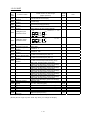
Table of contents
1. Investigation of the inverter
1.1 Specification label(Model name , Manufacturing number ; MFG)
1.1.1 Model name - - - - - - - - - - - - - - - - - - - - - - - - - - - - - - 1-1
1.1.2 MFG number - - - - - - - - - - - - - - -- - - - - - - - - - - - - - - 1-1
1.2 Inverter specification
1.2.1 SJ300 - - - - - - - - - - - - - - - - - - - - - - - - - - - - - - - - - - - - 1-2
1.2.2 L300P - - - - - - - - - - - - - - - - - - - - - - - - - - - - - - - - - - - - 1-10
2. Trouble shooting
2.1 INV trip contents , remedy , advice - - - - - - - - - - - - - - - - - - - 2-1
2.2 Option error
2.2.1 Feedback card - - - - - - - - - - - - - - - - - - - - - - - - - - - - - - 2-3
2.2.2 Digital option card - - - - - - - - - - - - - - - - - - - - - - - - - - - - - 2-3
2.3 Confirmation of the trip monitor contents - - - - - - - - - - - - - - - - - 2-3
2.4 Confirmation of the warning monitor contents - - -- - - - - - - - - - - 2-4
3. Debug mode
3.1 Monitor - - - - - - - - - - - - - - - - - - - - - - - - - - - - - - - - - - - - - - - - - 3-1
3.2 Parameter settings for inverter - - - - - - - - - - - - - - - - - - - - - - - - 3-2
4. Maintenance and Inspection
4.1 Maintenance and Inspection
4.1.1
Daily inspection - - - - - - - - - - - - - - - - - - - - - - - - - - - - 4-1
4.1.2
Cleaning - - - - - - - - - - - - - - - - - - - - - - - - - - - - - - - - - 4-1
4.1.3
Periodical inspection - - - - - - - - - - - - - - - - - - - - - - - - - 4-1
4.2 Daily and annual maintenance - - - - - - - - - - - - - - - - - - - - - - - - 4-2
4.3 Megger test - - - - - - - - - - - - - - - - - - - - - - - - - - - - - - - - - - - - - 4-3
4.4 Withstand voltage test - - - - - - - - - - - - - - - - - - - - - - - - - - - - 4-3
4.5 How to check inverter & converter portion - - - - - - - - - - - - - - - 4-4
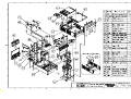
4.6 Parts replacement - - - - - - - - - - - - - - - - - - - - - - - - - - - - - - - - 4-5
4.7 Unit replacement - - - - - - - - - - - - - - - - - - - - - - - - - - - - - - - - - 4-8
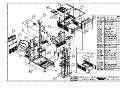
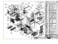
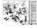
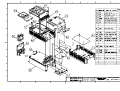
Appendix
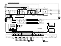
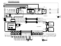
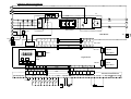
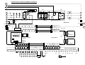
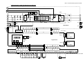
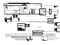
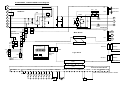
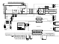
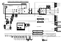
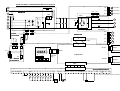
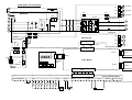
Circuit Diagram
Internal block diagram
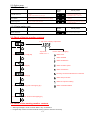
1. Investigation of the inverter
1.1 Specification label (Model name, Manufacturing number ; MFG)
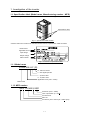
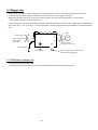
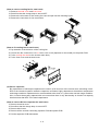
• There are 2 specification label attached to the inverter as shown in Fig 1-1.
Specification label
Fig 1-1 Specification label location
• Please confirm the model name and MFG number from the specification label as follows.
Model name
Applicable motor
Input ratings
Output ratings
MFG number
Fig 1-2 contents of specification label
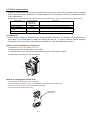
1.1.1 Model name
SJ300-055 H F (R)
R : with POT meter
F : with digital operator
L : 3φ 200V class
H : 3φ 400V class
Applicable motor (055 : 5.5kW)
Model name
1.1.2 MFG number
94 A T12345 9 0001
Serial No. (0001 ~ 9999)
Year of production (9 : 1999)
Production No.
REV. No.
Production year & month (94 : 1999 / April)
1-1
1.2 Inverter specification
(Note1)
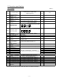
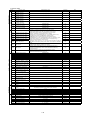
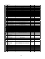
1.2.1 SJ300
Monitor Mode
Display
code
d001
d002
d003
d004
SJ300 monitor or data range
(digital operator)
Function name
Output frequency
monitor
Output current
monitor
Operation direction
monitor
PID feedback
monitor
0.00-99.99/100.0-400.0(Hz)
-
0.0-999.9(A)
-
F(forward)/o(stop)/r(reverse)
-
0.00-99.99/100.0-999.9/1000. –9999. /
1000-9999/{100-{999 (10000-99900)
-
(Example) FW, terminal 7,2,1: ON
Terminal 8,6,5,4,3:OFF
ON
FW
d005
Intelligent input
terminal monitor
-
OFF
8
d006
Initial
data
7 6
5
4
3 2
1
(Example) Terminal 12,11:ON
AL, 15,14,13:OFF
ON
Intelligent output
terminal monitor
-
OFF
AL 15 14 13 12
Frequency
0.00-99.99/100.0-999.9/1000. –9999. /
d007
conversion monitor
1000-3996
d012 torque monitor
-300.-+300.%
Output voltage
d013
0.0-600.0 V
monitor
Input electric power
d014
0.0-999.9 kW
monitor
Accumulated time
d016 monitor during
0.-9999./1000-9999/{100-{999 hr
RUN
Power ON time
d017
0.-9999./1000-9999/{100-{999 hr
monitor
Number of trip time
d080
0.-9999./1000-6553(10000-65530) (time)
monitor
d081 Trip monitor 1
d082 Trip monitor 2
d083 Trip monitor 3
Trip Code, frequency(Hz), current(A),
voltage(V),RUN time(hr) power ON time(hr)
d084 Trip monitor 4
d085 Trip monitor 5
d086 Trip monitor 6
d090 Warning monitor
Warning code
Output
frequency 0.0, starting frequency-Max. frequency
F001
0.00
setting
(2 nd max. 3 rd max. frequency)(Hz)
st
F002 1 acceleration time 0.01-99.99/100.0-999.9/1000. -3600.(s)
30.00
F202 2 nd acceleration time 0.01-99.99/100.0-999.9/1000. -3600.(s)
30.00
F302 3 rd acceleration time
0.01-99.99/100.0-999.9/1000. -3600.(s)
30.00
F003 1 st deceleration time 0.01-99.99/100.0-999.9/1000. -3600.(s)
30.00
F203 2 nd deceleration time 0.01-99.99/100.0-999.9/1000. -3600.(s)
30.00
F303 3 rd deceleration time 0.01-99.99/100.0-999.9/1000. -3600.(s)
30.00
Operation direction
F004
00(forward)/01(reverse)
00
selection
(Note1) Change mode during run by selection of b031 (software lock selection).
(Note2) Do not forget to press “STR” key when you change the display.
1 –2
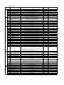
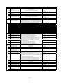
Note
Function Mode
V/f characteristic
Multistage speed,jogging frequency setting
Analog input setting
Base setting
Code
SJ300 Setting range
Initial data
-FE/-FU/-F
A001
Frequency setting selection
01(terminal)/02(operator)/03(RS485)/04(option1)/05(option2)
01/01/02
A002
Operation setting selection
01(terminal)/02(operator)/03(RS485)/04(option1)/05(option2)
01/01/02
A003
Base frequency
30. - Maximum. frequency(Hz)
50./60./60.
A203
Base frequency, 2nd motor
A303
Base frequency, 3rd motor
A004
Maximum frequency
30. – 400. (Hz)
50./60./60.
A204
Maximum frequency, 2nd motor
30. – 400. (Hz)
50./60./60.
A304
Maximum frequency, 3rd motor
30. – 400. (Hz)
50./60./60.
A005
AT terminal selection
00( Changing of O and OI with AT terminal)/
01(Changing of O and O2 with AT terminal)
00
A006
02 selection
A011
30. – 2nd Maximum. frequency (Hz)
30. -
3rd
Maximum. frequency (Hz)
50./60./60.
50./60./60.
00(single)/01(auxiliary speed of O, OI) [no reversible] /
02(auxiliary speed of O, OI [reversible]
00
0 start
0.00-99.99/100.0-400.0 (Hz)
0.00
A012
0 end
0.00-99.99/100.0-400.0 (Hz)
0.00
A013
0 start rate
0.-100.0 (%)
0.
A014
0 end rate
0.-100.0(%)
100.
00 (external starting frequency)/01(0Hz)
01
1.-30.(times)
8.
A015
0 start selection
A016
O, OI, O2 sampling
00(binary : range is to 16 stage speed with 4 terminals)/
01(bit : range is to 8 stage speed with 7 terminals)
00
0.00, starting frequency-maximum. frequency(Hz)
0.00
0.00
A019
Multi-speed selection
A020
Multi-speed 0
A220
Multi-speed 0, 2 nd motor
0.00, starting frequency-2 nd maximum frequency(Hz)
A320
Multi-speed 0, 3 rd motor
0.00, starting frequency-3 rd maximum frequency(Hz)
0.00
A021
Multi-speed1
0.00, starting frequency-maximum frequency(Hz)
0.00
A022
Multi-speed2
0.00, starting frequency-maximum frequency(Hz)
0.00
A023
Multi-speed3
0.00, starting frequency-maximum frequency(Hz)
0.00
A024
Multi-speed4
0.00, starting frequency-maximum frequency(Hz)
0.00
A025
Multi-speed5
0.00, starting frequency-maximum frequency(Hz)
0.00
A026
Multi-speed6
0.00, starting frequency-maximum frequency(Hz)
0.00
A027
Multi-speed7
0.00, starting frequency-maximum frequency(Hz)
0.00
A028
Multi-speed8
0.00, starting frequency-maximum frequency(Hz)
0.00
A029
Multi-speed9
0.00, starting frequency-maximum frequency(Hz)
0.00
A030
Multi-speed10
0.00, starting frequency-maximum frequency(Hz)
0.00
A031
Multi-speed11
0.00, starting frequency-maximum frequency(Hz)
0.00
A032
Multi-speed12
0.00, starting frequency-maximum frequency(Hz)
0.00
A033
Multi-speed13
0.00, starting frequency-maximum frequency(Hz)
0.00
A034
Multi-speed14
0.00, starting frequency-maximum frequency(Hz)
0.00
A035
Multi-speed15
0.00, starting frequency-maximum frequency(Hz)
0.00
A038
Jogging frequency
0.00, starting frequency-9.99(Hz)
1.00
A039
Jogging selection
00(free-run on JG stop / invalid on running) / 01(stop decelerating on
JG stop / invalid on running) / 02(DC braking on JG stop/invalid on
running) / 03(free-run on JG stop/valid on running[JG after stop
decelerating]) / 04 (stop decelerating on JG stop/valid on running) / 05
(DC braking on JG stop/valid on operating)
00
A041
Torque boost selection
00 (manual torque boost) / 01 (automatic torque boost)
00
A241
Torque
motor
00 (manual torque boost) / 01 (automatic torque boost)
00
A042
Manual torque boost
0.0-20.0(%)
1.0
A242
Manual torque boost, 2 nd motor
0.0-20.0(%)
1.0
A342
Manual torque boost, 3rd motor
0.0-20.0(%)
1.0
A043
Manual torque boost point
0.0-50.0(%)
5.0
A243
Manual torque boost point, 2 nd
motor
0.0-50.0(%)
5.0
A343
A044
Direct current braking
Function name
boost
selection,
2nd
Manual torque boost point, 3
motor
rd
1st control
nd
A244
2
A344
3rd control
control
A045
0.0-50.0(%)
5.0
00/(VC)/01(VP1.7power)/02(free V/f setting)/03(SLV)/
04(0Hz-SLV)/05(V2)
00
00/(VC)/01(VP1.7power)/02(free V/f setting) /03(SLV)/04(0Hz-SLV)
00
00/(VC)/01(VP1.7power)
00
Output voltage gain
20. - 100.
100.
A051
DC braking selection
00(invalid)/01(valid)
00
A052
DC braking frequency
0.00-60.00(Hz)
0.50
0.0 - 5.0(s)
0.0
A053
DC braking wait time
A054
DC braking power
0. - 100. (%)
0.
A055
DC braking time
0.0 - 60.0(s)
0.0
A056
DC braking edge/level selection
00(edge action)/01(level action)
01
A057
DC braking power (starting time)
0. - 100. (%)
0.
A058
DC braking time(starting time)
0.00-60.0(s)
0.0
A059
DC carrier frequency
0.5-15(kHz) Derating
5.0
1- 3
Note
Function Mode
Operation mode/ adjustable function
PID control
AVR
Upper and lower limiter,jump
frequency
Code
1st frequency maximum limiter
2nd frequency maximum limiter
1st frequency minimum limiter
2nd frequency minimum limiter
Jump frequency1
Jump frequency Width 1
Jump frequency2
Jump frequency Width 2
Jump frequency3
Jump frequency Width 3
Acceleration stop frequency
Acceleration stop time
PID selection
PID-P gain
PID-I gain
PID-D gain
PID scale
PID feedback selection
AVR selection
A082
Motor voltage selection
A085
A097
A098
A101
A102
A103
A104
A105
A111
A112
A113
A114
A131
Operation mode selection
Energy-saving responseaccuracy adjustment
Acceleration time2
Acceleration time2(2 nd motor)
Acceleration time2(3rd motor)
Deceleration time2
Deceleration time2(2 nd motor)
Deceleration time2(3rd motor)
2nd stage adjustable selection
2nd stage adjustable
selection(2 nd motor)
2nd acceleration frequency
2nd acceleration
frequency(2 nd motor)
2nd deceleration frequency
2nd deceleration frequency
(2nd motor)
Acceleration pattern selection
Deceleration pattern selection
OI start
OI end
OI start rate
OI end rate
OI start selection
O2 start
O2 end
O2 start rate
O2 end rate
Acceleration curve constant
A132
Deceleration curve constant
b001
Retry selection
A086
A092
A292
A392
A093
A293
A393
A094
A294
A095
A295
A096
Accel,
Decel
External frequency
adjustment
A296
Instantaneous power failure
restart
Function name
A061
A261
A062
A262
A063
A064
A065
A066
A067
A068
A069
A070
A071
A072
A073
A074
A075
A076
A081
b002
b003
b004
b005
b006
b007
Allowable under-voltage power
failure time
Retry wait time
Instantaneous power failure/
under-voltage trip during stop
Instantaneous power failure/
under-voltage retry time
selection
Open-phase selection
Frequency setting to match
SJ300 Setting range
0.00, 1st frequency lower limitter - maximum frequency(Hz)
0.00, 2 nd frequency lower limiter-2 nd setting maximum frequency(Hz)
0.00, start frequency-maximum frequency(Hz)
0.00, start frequency-2 nd setting maximum frequency(Hz)
0.00-99.99/100.0-400.0(Hz)
0.00-10.00(Hz)
0.00-99.99/100.0-400.0(Hz)
0.00-10.00(Hz)
0.00-99.99/100.0-400.0(Hz)
0.00-10.00(Hz)
0.00-99.99/100.0-400.0(Hz)
0.00-60.0(s)
00(invalid)/01(valid)
0.2-5.0
0.0-3600.(s)
0.00-100.0(s)
0.01-99.99(%)
00(feedback : OI)/01(feedback : O)
00(ON always)/01(OFF always)/02(OFF on decelerating)
200/215/220/230/240,
380/400/415/440/460/480
00(normal operation)/01(energy-saving operation)/02(Fuzzy)
Initial data
-FE/-FU
0.00
0.00
0.00
0.00
0.00
0.50
0.00
0.50
0.00
0.50
0.00
0.0
00
1.0
1.0
0.00
1.00
00
02
(230/400)/
(230/460)/
(200/400)
00
0.0-100.0
50.0
0.01-99.99/100.0-999.9/1000.-3600.(s)
0.01-99.99/100.0-999.9/1000.-3600.(s)
0.01-99.99/100.0-999.9/1000.-3600.(s)
0.01-99.99/100.0-999.9/1000.-3600.(s)
0.01-99.99/100.0-999.9/1000.-3600.(s)
0.01-99.99/100.0-999.9/1000.-3600.(s)
00(change with 2CH terminal)/01(change with setting)
15.00
15.00
15.00
15.00
15.00
15.00
00
00(change with 2CH terminal)/01(change with setting)
00
0.00-99.99/100.0-400.0(Hz)
0.00
0.00-99.99/100.0-400.0(Hz)
0.00
0.00-99.99/100.0-400.0(Hz)
0.00
0.00-99.99/100.0-400.0(Hz)
0.00
00(straight line)/01(S-curve)/02(U-curve)/03(reverse U-curve)
00(straight line)/01(S-curve)/02(U-curve)/03(reverse U-curve)
0.00-99.99/100.0-400.0(Hz)
0.00-99.99/100.0-400.0(Hz)
0.-100. (%)
0.-100. (%)
00(external start frequency)/01(0Hz)
-400.--100./-99.9-0.00-99.9/100.-400.(Hz)
-400.--100./-99.9-0.00-99.9/100.-400.(Hz)
-100. - 100. (%)
-100. - 100. (%)
01(small swelling)-10(large swelling)
00
00
0.00
0.00
20.
100.
01
0.00
0.00
-100.
100.
02
01(small swelling-10(large swelling)
02
00(trip)/01(0Hz start)/02(start after equal frequency)/
03(trip after equaling frequency and deceleration stop)
00
0.3-1.0(s)
1.0
0.3-100.(s)
00(invalid/01(valid)/02(invalid during stop and deceleration by stop
command)
1.0
00(16 times)/01(free)
00
00(invalid)/01(valid)
0.00-99.99/100.0-400.0(Hz)
00
0.00
1- 4
00
Note
Function mode
Code
Function name
b012
Electronic thermal level
0.2*constant current-1.20*constant current(A)
b212
Electronic thermal level
(2nd motor)
0.2*constant current-1.20*constant current(A)
b312
Electronic thermal level
(3rd motor)
0.2*constant current-1.20*constant current(A)
st
Electronic thermal
b013
b213
b313
b015
b016
b017
b018
b019
Free V/f setting
Overload limit
b020
Intelligent input terminal setting
SJ300 Setting range
1 electronic thermal
characteristic selection
2nd electronic thermal
characteristic selection
3rd electronic thermal
characteristic selection
Free electronic thermal
frequency 1
Free electronic thermal
current 1
Free electronic thermal
frequency 2
Free electronic thermal
current 2
Free electronic thermal
frequency 3
Free electronic thermal
current 3
b021
Overload restriction selection
b022
Overload restriction level
b023
Overload restriction limit
constant
b024
Overload restriction 2
selection
b025
Overload restriction level 2
b026
Overload restriction constant
2
b031
Software lock mode selection
b100
b101
b102
b103
b104
b105
b106
b107
b108
b109
b110
b111
b112
b113
Free
Free
Free
Free
Free
Free
Free
Free
Free
Free
Free
Free
Free
Free
C001
Intelligent input 1 setting
C002
Intelligent input 2 setting
C003
Intelligent input 3 setting
C004
Intelligent input 4 setting
C005
Intelligent input 5 setting
C006
Intelligent input 6 setting
C007
Intelligent input 7 setting
C008
Intelligent input 8 setting
V/f
V/f
V/f
V/f
V/f
V/f
V/f
V/f
V/f
V/f
V/f
V/f
V/f
V/f
frequency
voltage 1
frequency
voltage 2
frequency
voltage 3
frequency
voltage 4
frequency
voltage 5
frequency
voltage 6
frequency
voltage 7
1
2
3
4
5
6
7
00(reduced characteristic)/ 01(constant torque characteristic)/
02(free setting)
00(reduced characteristic)/ 01(constant torque characteristic)/
02(free setting)
00/(reduced characteristic)01(constant torque characteristic)/
02(free setting)
Initial data
-FE/-FU/-F
Rated
Current of
inverter
Rated
Current of
Inverter
Rated
current of
inverter
01/01/00
01/01/00
01/01/00
0.-400.(Hz)
0.
0.0-1000.(A)
0.0
0.-400.(Hz)
0.
0.0-1000. (A)
0.0
0.-400.(Hz)
0.
0.0-1000.(A)
0.0
00(invalid)/01(enabled on acceleration / constant speed)/
02(enabled on constant speed)/03(enabled on acceleration / constant
speed (speed increasing at regenerating mode))
01
0.50* rated current-2.00* rated current(A)
Rated current
of Inverter
x 1.50
0.10-30.00(s)
1.00
00(invalid)/01(enabled on acceleration / constant speed)/
02(enabled on constant speed)/03(enabled on acceleration / constant
speed (speed increasing at regenerating mode))
01
0.50*rated current-2.00*rated current(A)
Rated current
of inverter
x1.50
0.10-30.00(s)
1.00
00(impossible to change the data except this item when SFT terminal is
ON)/01(impossible to change the data except setting frequency item
when SFT terminal is ON)/02(impossible to change the data except this
item)/
03(impossible to change the data except setting frequency item)/
10(possible to change data on operating)
0.- Free V/f frequency2(Hz)
0.-800.0(V)
0.- Free V/f frequency3(Hz)
0.-800.0(V)
0.- Free V/f frequency4(Hz)
0.-800.0(V)
0.- Free V/f frequency5(Hz)
0.-800.0(V)
0.- Free V/f frequency6(Hz)
0.-800.0(V)
0.- Free V/f frequency7(Hz)
0.-800.0(V)
0.-400.(Hz)
0.-800.0(V)
01/(RV:Reverse is valid)/02(CF1:Multi-speed1)/ 03(CF2:Multi-speed2)/
04(CF3:Multi-speed3)/ 05(CF4:Multi-speed4)/ 06(JG:Jogging)/
07(DB:External DC braking)/ 08(SET:2 nd control)/
09(2CH:two-stage adjustable speed)/ 11(FRS:Free-run)/ 12(EXT:External
trip)/
13(USP:Unattended start protection)/ 14(CS:commercial change)/
15(SFT:software lock)/ 16(AT:Analog input voltage/current select)/
17(SET3:3 rd control)/ 18(RS:Reset inverter)/ 20(STA:3wire run)/
21(STP:3wire keep)/ 22(F/R:3wire forward/reverse)/
23(PID:PID selection valid/invalid)/ 24(PIDC:PID integrating reset)/
26(CAS:Control gain switch function)/ 27(UP:Remote control UP function)/
28(DWN:Remote control DOWN function)/29(UDC:Remote control data clear)/
31(OPE:Operating by operator select)/ 32(SF1:Multi-speed bit1)/
33(SF2:Multi-speed bit2)/ 34(SF3:Multi-speed bit3)/ 35(SF4:Multi-speed bit4)/
36(SF5:Multi speed bit5)/ 37(SF6:Multi-speed bit6)/ 38(SF7:Multi-speed bit7)/
39(OLR:Overload restriction change) / 40(TL:Torque limit select)/
41(TRQ1:Torque limit switch 1)/ 42(TRQ2:Torque limit switch 2)/
43((PPI:P/PI switch)/ 44(BOK:Braking comformation)/ 45(ORT:Orientation)/
46(LAC:LAD cancel)/ 47(PCLR:Position error clear)/
48(STAT:Permission of pulse train)/ no(NO:No assign)
1- 5
01
0.
0.0
0.
0.0
0.
0.0
0.
0.0
0.
0.0
0.
0.0
0.
0.0
18
16
06
11
09
03/13/03
02
01
Note
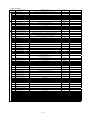
Function mode
Code
C011
Input terminal setting
intelligent
C012
C013
C014
C015
C016
C017
C018
Intelligent output terminal setting
C019
Intelligent output 11 setting
C022
Intelligent output 12 setting
C023
Intelligent output 13 setting
C024
Intelligent output 14 setting
C025
Intelligent output 15 setting
C026
Alarm relay output
C027
FM selection
C028
AM selection
state
terminal
setting,Output level setting
Output
SJ300 Setting range
Initial data
-FE/-FU/-F
00(NO)/01(NC)
00
00(NO)/01(NC)
00
00(NO)/01(NC)
00
00(NO)/01(NC)
00
00(NO)/01(NC)
00
00(NO)/01(NC)
00/01/00
00(NO)/01(NC)
00
00(NO)/01(NC)
00
00(NO)/01(NC)
00
00(RUN:running)/01(FA1:Frequency arrival type1 signal)/
02(FA2:over setting frequency)/03(OL:Overload advance notice signal)/
04(OD:Output deviation for PID control)/05(AL:Alarm signal)/
06(FA3:Only setting frequency)/07(OTQ:Over-torque signal)/
08(IP:On instantaneous stop)/09(UV:Under voltage)/
10(TRQ:Torque limit)/11(RNT:RUN time over/12(ONT:ON time over)/
13(THM:thermal caution)/19(BRK:Brake release signal)/
20(BER:Brake error signal)/21(ZS:Zero speed detect signal)/
22(DSE:Speed error over signal)/23(POK:Positioning completion signal)
24(FA4:Over frequency 2 signal)/25(FA5:Only setting frequency)/
26(OL2: Overload advance notice signal 2)
(Intelligent output terminal 11-13 or 11-14 becomes AC0-AC2 or AC0-AC3
(Can:Alarm cord output) forcibly when alarm cord output is selected in
C062)
00(Output frequency)/01(Output current) /02(Output torque)/
03(Digital output frequency)/04(Output voltage)/
05(Input electric power)/06(thermal load rate)/07(LAD frequency)
00(Output frequency)/01(Output current)/02(Output torque)/
04(Output voltage)/05(Input electric power)/06(thermal load rate)/
07(LAD frequency)
00(Output frequency)/01(Output current)/02(Output torque)/
04(Output voltage)/05(Input electric power)/
06(Thermal load rate)/07(LAD frequency)
00(NO)/01(NC)
00(NO)/01(NC)
00(NO)/01(NC)
00(NO)/01(NC)
00(NO)/01(NC)
00(NO)/01(NC)
01
00
03
07
08
05
00
00
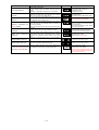
C029
AMI selection
C031
C032
C033
C034
C035
C036
C072
C073
C074
C075
C078
Intelligent output 11 a/b
Intelligent output 12 a/b
Intelligent output 13 a/b
Intelligent output 14 a/b
Intelligent output 15 a/b
Alarm relay output a/b
Overload advance notice
signal output mode
Overload advance notice
level
Frequency arrival setting for
acceleration.
Arrival frequency setting for
deceleration.
PID deviation setting level
Frequency arrival setting for
acceleration 2.
Arrival frequency setting for
deceleration 2.
Over torque level setting
(Forward-driving)
Over torque level setting
(Reverse-regenerating)
Over torque level setting
(Reverse-driving)
Over torque level setting
(Forward-regenerating)
Thermal warning level
setting
Alarm code selection
Zero speed detection level
setting
Data command
Communicating transmission
speed
Communication code
Communication bit
Communication parity
Communication stop bit
Communication waiting time
C081
O adjustment
0.-9999./1000-6553(10000-65530)
C082
OI adjustment
0.-9999./1000-6553(10000-65530)
C083
O2 adjustment
0.-9999./1000-6553(10000-65530)
Setting on
forwarding
Setting on
forwarding
Setting on
forwarding
C085
C086
C087
Thermistor adjustment
AM offset adjustment
AMI adjustment
0.0 - 1000.
0.0 - 10.0(V)
0. - 255.
105.0
0.0
80
C088
AMI offset adjustment
0. - 20.0(mA)
Setting on
forwarding
C041
C042
C043
C044
C045
C046
C055
C056
C057
C058
C061
C062
C063
Communication
function adjustment
Intelligent input 1 a/b
(NO/NC) selection
Intelligent input 2 a/b
(NO/NC) selection
Intelligent input 3 a/b
(NO/NC) selection
Intelligent input 4 a/b
(NO/NC) selection
Intelligent input 5 a/b
(NO/NC) selection
Intelligent input 6 a/b
(NO/NC) selection
Intelligent input 7a/b
(NO/NC) selection
Intelligent input 8 a/b
(NO/NC) selection
Input FW a/b (NO/NC)
Selection
C021
C040
Analog meter setting
Function name
C070
C071
00
00
00
00
00
00
01
00(On accel. And decel, constant speed)/01(Only constant speed)
01
0.0-2.0*rated current(A)
Inverter
rated current
0.00-99.99/100.0-400.0(Hz)
0.00
0.00-99.99/100.0-400.0(Hz)
0.00
0.0-100.0(%)
3.0
0.00-99.99/100.0-400.0(Hz)
0.00
0.00-99.99/100.0-400.0(Hz)
0.00
0.-200.(%)
100.
0.-200.(%)
100.
0.-200.(%)
100.
0.-200.(%)
100.
0.-100.(%)
80.
00(Invalid)/01(3bit)/02(4bit)
00
0.00-99.99/100.(Hz)
0.00
02(operator)/03(RS485)/04(option1)/05(option2)
02(loop-back test)
03(2400bps)/04(4800bps)/05(9600bps)/06(19200bps)
1. -32.
7(7bit)/8(8bit)
00(no parity name)/01(even parity)/02(odd parity)
1(bit)/2(bit)
0.-1000.(ms)
02
1- 6
04
1.
7
00
1
0.
Note
Function mode
Code
RUN time/Power ON time level
0.-9999./1000-6553(10000-65530)hr
00(Reverse is valid)/01(Only forward)/02(Only reverse)
00(Start reduced voltage time small)-06(Start reduced voltage time large)
00(all display)/01(each function display)/02(User setting / main setting)
00(4 quadrant mode)/01(Terminal operation)/
02(Analog input)/03(Option1)/04(Option2)
0.
00
06
00
0.-200.(%)/no(Invalid)
150.
0.-200.(%)/no(Invalid)
150.
0.-200.(%)/no(Invalid)
150.
0.-200.(%)/no(Invalid)
150.
00(Invalid)/01(Valid)
00
00(Invalid)/01(Valid)
00
00(Invalid)/01(Valid)
00
0.0-1000.(V)
0.0
0.0-1000.(V)
0.0
0.01-99.99/100.0-999.9/1000.-3600.(s)
1.00
0.00-10.00(Hz)
0.00
0. - 255.
0. - 255.
0.10-9.99(Hz)
0.5-15.0(kHz) Derating enable,
00(Trip history clear)/01(Data initialization)/
02(Trip history clear + data initialization)
00(Interior)/01(EC)/02(USA)
180
60
0.50
5.0
01/02/00
0.1-99.9
1.0
00(valid)/01(invalid)
00
Operation direction restrict
Start reduced voltage
Display selection
b040
Torque limit mode selection
b080
b081
b082
b083
Torque limit level 1 setting
(Forward-driving at
4 quadrant mode)
Torque limit level 2 setting
(Reverse-regenerating at
4 quadrant mode)
Torque limit level 3 setting
(Reverse-driving at
4 quadrant mode)
Torque limit level 4 setting
(Forward-regenerating at
4 quadrant mode)
Torque LAD-STOP selection
Reverse run prevention
selection
Selection of non-stop
function at instantaneous
power failure
Start voltage of non-stop
function setting
OV LAD-STOP level of nonstop function setting
Deceleration time of nonstop function setting
Deceleration frequency width
of non-stop function setting
AM adjustment
FM adjustment
Start frequency adjustment
Carrier frequency setting
b084
Initialize mode
b085
b090
b091
Country code for initialization
Frequency scalar conversion
factor
STOP key enable
Resume on FRS cancellation
mode
BRD usage ratio
Stop mode selection
b092
Cooling fan control
b095
b096
b098
b099
b120
BRD selection
BRD ON level
Thermistor selection
Thermistor error level
Braking control selection
Waiting time for releasing
braking conformation
Waiting time for acceleration
Waiting time for stop
Waiting time for signal
conformation
Releasing frequency
b042
b043
b044
b045
b046
b050
b051
b052
The others
SJ300 Setting range
b034
b035
b036
b037
b041
b053
b054
b086
b087
b088
b121
b122
b123
b124
b125
Initial data
-FE/-FU/-F
Function name
00
0.0-100.0(%)
00(deceleration stop)/01(Free-run stop)
00(Always ON)/
01(ON during run, After power ON, then for 5 minutes on stop is implied.)
00(invalid)/01(valid<invalid during stop>)/02(valid<valid during stop>)
330-380/660-760(V)
00(invalid)/01(Positive temperature coefficient enable)/02 (NTC enable)
0. - 9999. (ohm)
00(Invalid)/01(valid)
0.0
00
00
360/720
00
3000.
00
0.00-5.00(s)
0.00
0.00-5.00(s)
0.00-5.00(s)
0.00
0.00
00
0.00-5.00(s)
0.00
0.00-99.99/100.0-400.0(Hz)
0.00
Rated
current of
inverter
00
00
b126
Releasing current
Debug mode selection
UP/DWN selection
0.00*rated current-2.00*rated current(A)
C102
Reset selection
C103
Reset f frequency matching
selection
C111
Overload
level
C121
O zero adjustment
C122
OI zero adjustment
0.-9999./1000-6553(10000-65530)
C123
O2 zero adjustment
0.-9999./1000-6553(10000-65530)
00(No display)/01(Display)
00(No frequency data)/01(Keep frequency data)
00(Trip cancel during ON)/01(Trip cancel during OFF)/
02(Valid only during trip<Cancel during ON>)
notice
00
00(0Hz start)/01(Start f-equaling)
C091
C101
advance
00
00
00(0Hz start)/01(Start f-equaling)
00
0.0-2.0*rated current(A)
Inverter
rated
current
0.-9999./1000-6553(10000-65530)
1- 7
Set on
forwarding
Set on
forwarding
Set on
forwarding
Note
Function mode
The others
Code
Function name
H001
Autotuning selection
H002
1st motor constant selection
H202
2nd motor constant selection
Initial data
-FE/-FU/-F
SJ300 Setting range
00(Invalid)/01(Valid(the motor does not rotate))/
02(Valid(the motor rotates))
00(Hitachi general purpose motor data)/01(Autotuning data)/
02(Autotuning data with online autotuning)
00(Hitachi general purpose motor data)/01(Autotuning data)/
02(Autotuning data with online autotuning)
00
00
00
H003
1 allowable motor selection
0.20-75.0(kW)
H203
2nd allowable motor selection
0.20-75.0(kW)
Set on
forwarding
Set on
forwarding
H004
H204
H005
H205
H006
H206
H306
1st motor pole selection
2nd motor pole selection
1st speed response setting
2nd speed response setting
1st stabilized factor
2nd stabilized factor
3rd stabilized factor
2/4/6/8(pole)
2/4/6/8(pole)
0.001-9.999/10.00-65.53
0.001-9.999/10.00-65.53
0. - 255.
0. - 255.
0. - 255.
4
4
1.590
1.590
100.
100.
100.
H020
1st motor constant R1
st
nd
0.000-9.999/10.00-65.53(ohm)
Set on
forwarding
Set on
forwarding
Set on
forwarding
Set on
forwarding
Set on
forwarding
Set on
forwarding
Set on
forwarding
Set on
forwarding
Set on
forwarding
Set on
forwarding
Set on
forwarding
0.000-9.999/10.00-65.53(ohm)
Set on
forwarding
0.000-9.999/10.00-65.53(ohm)
Set on
forwarding
0.000-9.999/10.00-65.53(ohm)
Set on
forwarding
0.00-99.99/100.0-655.3(mH)
Set on
forwarding
0.00-99.99/100.0-655.3(mH)
Set on
forwarding
0.00-99.99/100.0-655.3(A)
Set on
forwarding
0.000-9.999/10.00-65.53(ohm)
H220
2
motor constant R1
0.000-9.999/10.00-65.53(ohm)
H021
1st motor constant R2
0.000-9.999/10.00-65.53(ohm)
H221
2nd motor constant R2
0.000-9.999/10.00-65.53(ohm)
H022
1st motor constant L
0.00-99.99/100.0-655.3(mH)
H222
2nd motor constant L
0.00-99.99/100.0-655.3(mH)
H023
1st motor constant I 0
0.00-99.99/100.0-655.3(A)
H223
2nd motor constant I 0
0.00-99.99/100.0-655.3(A)
H024
1st motor constant J
0.001-9.999/10.00-99.99/100.0-9999.(kgm2 )
H224
2nd motor constant J
0.001-9.999/10.00-99.99/100.0-9999.(kgm2 )
H030
H230
H031
H231
H032
H232
H033
1st motor constant R1
(Autotuning data)
2nd motor constant R1
(Autotuning data)
1st motor constant R2
(Autotuning data)
2nd motor constant R2
(Autotuning data)
1st motor constant L
(Autotuning data)
2nd motor constant L
(Autotuning data)
1st motor constant I 0
(Autotuning data)
2nd motor constant I 0
(Autotuning data)
H034
1 motor constant J
0.001-9.999/10.00-99.99/100.0-9999.(kgm )
H234
2nd motor constant J
0.001-9.999/10.00-99.99/100.0-9999.(kgm2 )
Set on
forwarding
Set on
forwarding
Set on
forwarding
0.00-99.99/100.0-999.9/1000.(%)
100.0
0.00-99.99/100.0-999.9/1000.(%)
100.0
H233
st
0.00-99.99/100.0-655.3(A)
2
st
H050
H250
H051
H251
H052
H252
H060
H260
H070
H071
H072
1 PI-control proportion gain
setting
2nd PI-control proportion gain
setting
1st PI-control integration gain
setting
2nd PI-control integration gain
setting
1st P-control proportion gain
setting
2nd P-control proportion gain
setting
1st 0Hz-SLV limiter setting
2nd 0Hz-SLV limiter setting
PI-control proportion gain for
switching
PI-control integration gain for
switching
P-control proportion gain for
switching
0.00-99.99/100.0-999.9/1000.(%)
100.0
0.00-99.99/100.0-999.9/1000.(%)
100.0
0.01-10.00
1.00
0.01-10.00
1.00
0.-100.(%)
0.-100.(%)
100.
100.
0.00-99.99/100.0-999.9/1000.(%)
100.0
0.00-99.99/100.0-999.9/1000.(%)
100.0
0.00-10.00
1.00
1- 8
Note
Function mode
Code
U001
U002
U003
U004
U005
U006
U007
U008
U009
U010
U011
U012
User2 selection
User3 selection
User4 selection
User5 selection
User6 selection
User7 selection
User8 selection
User9 selection
User10 selection
User11 selection
User12 selection
P001
P002
P010
P011
P012
P013
P014
P015
P016
Option
P017
P018
P019
P020
P021
P022
P023
P025
P026
P027
P031
P032
User selection
Function name
Option1 operation selection
on error
Option2 operation selection
on error
Feed-back option selection
Encoder pulse number
setting
Control mode selection
Pulse train input mode
selection
Orientation stop position
setting
Orientation speed setting
Orientation direction
selection
Orientation completion range
setting
Orientation completion delay
time setting
Electronic gear position
selection
Electronic gear numerator of
ratio setting
Electronic gear denominator
of ratio setting
Position control feed-forward
gain setting
Position control loop gain
setting
Compensation of secondary
resistor selection
Over-speed detect level
setting
Speed-error over detect level
setting
Digital input option input
mode selection (Acc/Dec)
Stop position setting for
orientation
input
mode
selection
User1 selection
SJ300 Setting range
Initial data
-FE/-FU/-F
00(TRP)/01(RUN)
00
00(TRP)/01(RUN)
00
00(Invalid)/01(Valid)
00
128.-9999./1000-6500(10000-65000) (pulse)
1024
00(ASR mode)/01(APR mode)
00
00(Mode 0)/01(Mode 1)/02(Mode 2)/03(Mode 3)
00
0.-4095.
0.
0.00-99.99/100.0-120.0(Hz)
5.00
00(Forward)/01(Reverse)
00
0.-9999./1000(10000) (pulse)
5
0.00-9.99(s)
0.00
00(Feedback)/01(Reference)
00
0.-9999.
1.
0.-9999.
1.
0.00-99.99/100.0-655.3
0.00
0.00-99.99/100.0
0.50
00(Invalid)/01(Valid)
00
0.00-99.99/100.0-150.0(%)
135.0
0.00-99.99/100.0-120.0(Hz)
7.50
00(operator)/01(option1)/02(option2)
00
00(operator)/01(option1)/02(option2)
00
no/d001-P032
no
no/d001-P032
no/d001-P032
no/d001-P032
no/d001-P032
no/d001-P032
no/d001-P032
no/d001-P032
no/d001-P032
no/d001-P032
no/d001-P032
no/d001-P032
no
no
no
no
no
no
no
no
no
no
no
1- 9
Note
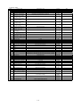
1.2.2 L300P
Monitor code
Display
code
d001
d002
d003
d004
L300P monitor or data range
(digital operator)
Function name
Output frequency
monitor
Output current
monitor
Operation direction
monitor
PID feedback
monitor
0.00-99.99/100.0-400.0(Hz)
-
0.0-999.9(A)
-
F(forward)/o(stop)/r(reverse)
-
0.00-99.99/100.0-999.9/1000. -9999. /
1000-9999/{100-{999 (10000-99900)
-
(Example) FW, terminal2, and 1: ON
Terminal 5, 4, 3 :OFF
ON
FW
d005
Initial
data
Intelligent input
terminal monitor
-
OFF
5 4
d006
(Example) Terminal2, 1:ON
AL :OFF
Intelligent output
terminal monitor
d013
d014
d016
d017
d080
Frequency
conversion monitor
Output voltage
monitor
Electric power
monitor
Accumulated time
monitor during RUN
Power ON time
monitor
Number of trip time
monitor
d081
Trip monitor 1
d082
Trip monitor 2
d083
Trip monitor 3
d084
Trip monitor 4
d085
Trip monitor 5
d086
Trip monitor 6
d090
1
ON
AL
d007
3 2
12
OFF
11
0.00-99.99/100.0-999.9/1000. –9999. /
1000-3996
-
0.0-600.0
-
V
0.0-999.9 kW
-
0.-9999./1000-9999/{100-{999 hr
-
0.-9999./1000-9999/{100-{999 hr
-
0.-9999./1000-6553(10000-65530) (time)
-
Trip Code, frequency(Hz), current(A),
voltage(V),RUN time(hr) power ON time(hr)
Trip Code, frequency(Hz), current(A),
voltage(V),RUN time(hr) power ON time(hr)
Trip Code, frequency(Hz), current(A),
voltage(V),RUN time(hr) power ON time(hr)
Trip Code, frequency(Hz), current(A),
voltage(V),RUN time(hr) power ON time(hr)
Trip Code, frequency(Hz), current(A),
voltage(V),RUN time(hr) power ON time(hr)
Trip Code, frequency(Hz), current(A),
voltage(V),RUN time(hr) power ON time(hr)
Warning code
0.0, starting frequency-Max. frequency
(2 nd max. frequency)(Hz)
0.01-99.99/100.0-999.9/1000.-3600.(s)
0.01-99.99/100.0-999.9/1000. -3600. (s)
0.01-99.99/100.0-999.9/1000. -3600. (s)
0.01-99.99/100.0-999.9/1000. -3600. (s)
-
Warning monitor
Output
frequency
0.00
F001
setting
st
F002 1 acceleration time
30.00
F202 2 nd acceleration time
30.00
F003 1 st deceleration time
30.00
F203 2 nd deceleration time
30.00
Operation direction
F004
00(forward)/01(reverse)
00
selection
(Note1) Change mode during run by selection of b031 (software lock selection).
(Note2) Do not forget to press “STR” key when you change the display.
1 -10
Note
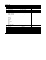
Function Mode
L300P Setting range
Initial data
-FE/-FU/-FR
Frequency setting selection
00(VR)/01(terminal)/02(operator)/03(RS485)/
04(option1)/05(option2)
01/01/00
A002
Operation setting selection
01(terminal)/02(operator)/03(RS485)/04(option1)/05(option2)
01/01/02
A003
Base frequency
30. - Maximum. frequency(Hz)
50./60./60.
A203
Base frequency, 2nd motor
30. - 2 nd Maximum. frequency (Hz)
50./60./60.
A004
Maximum frequency
30. - 400. (Hz)
50./60./60.
A204
Maximum frequency, 2nd
motor
30. - 400. (Hz)
50./60./60.
A005
AT terminal selection
00( Changing of O and OI with AT terminal)/01(Changing of O and O2
with AT terminal)
00
00(single)/01(auxiliary speed of O, OI) [no reversible]
/02(auxiliary speed of O, OI [reversible]
00
Code
Direct current braking
V/f characteristic
Multistage speed,jogging frequency setting
Analog input setting
Base setting
A001
A006
Function name
02 selection
A011
0 start
0.00-99.99/100.0-400.0 (Hz)
0.00
A012
0 end
0.00-99.99/100.0-400.0 (Hz)
0.00
A013
0 start rate
0.-100.0 (%)
0.
A014
0 end rate
0.-100.0(%)
100.
A015
0 start selection
00 (external starting frequency)/01(OHz)
01
A016
O, OI, O2 sampling
A019
Multi-speed selection
A020
Multi-speed 0
A220
Multi-speed 0, 2 nd motor
A021
1.-30.(times)
8.
00(binary : range is to 16 stage speed with 4 terminals)/01(bit : range
is to 6 stage speed with 5 terminals)
00
0.00, starting frequency-maximum. frequency(Hz)
0.00
0.00, starting frequency-2 nd maximum frequency(Hz)
0.00
Multi-speed1
0.00, starting frequency-maximum frequency(Hz)
0.00
A022
Multi-speed2
0.00, starting frequency-maximum frequency(Hz)
0.00
A023
Multi-speed3
0.00, starting frequency-maximum frequency(Hz)
0.00
A024
Multi-speed4
0.00, starting frequency-maximum frequency(Hz)
0.00
A025
Multi-speed5
0.00, starting frequency-maximum frequency(Hz)
0.00
A026
Multi-speed6
0.00, starting frequency-maximum frequency(Hz)
0.00
A027
Multi-speed7
0.00, starting frequency-maximum frequency(Hz)
0.00
A028
Multi-speed8
0.00, starting frequency-maximum frequency(Hz)
0.00
A029
Multi-speed9
0.00, starting frequency-maximum frequency(Hz)
0.00
A030
Multi-speed10
0.00, starting frequency-maximum frequency(Hz)
0.00
A031
Multi-speed11
0.00, starting frequency-maximum frequency(Hz)
0.00
A032
Multi-speed12
0.00, starting frequency-maximum frequency(Hz)
0.00
A033
Multi-speed13
0.00, starting frequency-maximum frequency(Hz)
0.00
A034
Multi-speed14
0.00, starting frequency-maximum frequency(Hz)
0.00
A035
Multi-speed15
0.00, starting frequency-maximum frequency(Hz)
0.00
A038
Jogging frequency
0.00, starting frequency-9.99(Hz)
1.00
A039
Jogging selection
00(free-run on JG stop / invalid on running) / 01(stop decelerating on
JG stop / invalid on running) / 02(DC braking on JG stop/invalid on
running) / 03(free-run on JG stop/valid on running[JG after stop
decelerating]) / 04 (stop decelerating on JG stop/valid on running) /
05 (DC braking on JG stop/valid on operating)
00
A041
Torque boost selection
00 (manual torque boost) / 01 (automatic torque boost)
00
A241
Torque
motor
00 (manual torque boost) / 01 (automatic torque boost)
00
1.0
boost
selection,
2 nd
A042
Manual torque boost
0.0-20.0(%)
A242
Manual torque boost, 2 nd motor
0.0-20.0(%)
1.0
A043
Manual torque boost point
0.0-50.0(%)
5.0
A243
Manual torque boost point, 2 nd
motor
0.0-50.0(%)
5.0
00
st
A044
1 control
00/(VC)/01(VP1.7power)/02(free V/f setting)
A244
2 nd control
00/(VC)/01(VP1.7power)/02(free V/f setting)
00
A045
Output voltage gain
20. - 100. (%)
100.
A051
DC braking selection
00(invalid)/01(valid)
00
A052
DC braking frequency
0.00-60.00(Hz)
0.50
A053
DC braking wait time
0.0 - 5.0(s)
0.0
A054
DC braking power
0. - 70. (%)
0.
A055
DC braking time
0.0 - 60.0(s)
0.0
A056
DC braking edge/level
selection
00(edge action)/01(level action)
01
A057
DC braking power
(starting time)
0. - 70. (%)
0.
A058
DC braking time
(starting time)
0.00-60.0(s)
0.0
A059
DC carrier frequency
0.5-12(kHz) Derating
3.0
1- 11
No t e
Function Mode
Instantaneous power failure
restart
Accel External frequency
Decel adjustment
Operation mode/ adjustable function
AVR PID control
Upper and lower limiter / jump
frequency
Code
L300P Setting range
1 s t frequency upper limiter
2 nd frequency upper limiter
A062
A262
A063
A064
A065
A066
A067
A068
A069
A070
A071
A072
A073
A074
A075
A076
A081
1 s t frequency lower limiter
2 nd frequency lower limiter
Jump frequency1
Jump frequency Width 1
Jump frequency2
Jump frequency Width 2
Jump frequency3
Jump frequency Width 3
Acceleration stop frequency
Acceleration stop time
PID selection
PID-P gain
PID-I gain
PID-D gain
PID scale
PID feedback selection
AVR selection
A082
Motor voltage selection
200/215/220/230/240, 380/400/415/440/460/480
A085
Operation mode selection
Energy-saving responseaccuracy adjustment
Acceleration time2
2 nd acceleration time2
Deceleration time2
2 nd deceleration time2
2 nd stage adjustable selection
2 nd stage adjustable
selection(2 nd motor)
2 nd acceleration frequency
2 nd acceleration
frequency(2 nd motor)
2 nd deceleration frequency
2 nd deceleration frequency
(2 nd motor)
Acceleration pattern selection
Deceleration pattern selection
OI start
OI end
OI start rate
OI end rate
OI start selection
O2 start
O2 end
O2 start rate
O2 end rate
Acceleration curve constant
00(normal operation)/01(energy-saving operation)
A086
A092
A292
A093
A293
A094
A294
A095
A295
A096
A296
A097
A098
A101
A102
A103
A104
A105
A111
A112
A113
A114
A131
A132
Deceleration curve constant
b001
Retry selection
0.00, 1 s t frequency lower limiter-maximum frequency(Hz)
0.00, 2 nd frequency lower limiter-2 nd setting maximum
frequency(Hz)
0.00, start frequency-maximum frequency(Hz)
0.00, start frequency-2 nd setting maximum frequency(Hz)
0.00-99.99/100.0-400.0(Hz)
0.00-10.00(Hz)
0.00-99.99/100.0-400.0(Hz)
0.00-10.00(Hz)
0.00-99.99/100.0-400.0(Hz)
0.00-10.00(Hz)
0.00-99.99/100.0-400.0(Hz)
0.00-60.0(s)
00(invalid)/01(valid)
0.2-5.0
0.0-3600.(s)
0.00-100.0(s)
0.01-99.99
00(feedback : OI)/01(feedback : O)
00(ON always)/01(OFF always)/02(OFF on decelerating)
50.0
15.00
15.00
15.00
15.00
00
00(change with 2CH terminal)/01(change with setting)
00
0.00-99.99/100.0-400.0(Hz)
0.00
0.00-99.99/100.0-400.0(Hz)
0.00
0.00-99.99/100.0-400.0(Hz)
0.00
0.00-99.99/100.0-400.0(Hz)
0.00
00(straight line)/01(S-curve)/02(U-curve)/03(reverse U-curve)
00(straight line)/01(S-curve)/02(U-curve)/03(reverse U-curve)
0.00-99.99/100.0-400.0(Hz)
0.00-99.99/100.0-400.0(Hz)
0.-100. (%)
0.-100. (%)
00(external start frequency)/01(0Hz)
-400.--100./-99.9-0.00-99.9/100.-400.(Hz)
-400.--100./-99.9-0.00-99.9/100.-400.(Hz)
-100. - 100. (%)
-100. - 100. (%)
01(small swelling)-10(large swelling)
00
00
0.00
0.00
20.
100.
01
0.00
0.00
-100.
100.
02
01(small swelling-10(large swelling)
00(trip)/01(0Hz start)/02(start after equal frequency)/
03(trip after equaling frequency and deceleration stop)
02
0.3-1.0(s)
1.0
0.3-100.(s)
1.0
00(invalid/01(valid)/
02(invalid during stop and deceleration by stop command)
00
b012
Electronic thermal level
0.2*constant current-1.20*constant current(A)
b212
Electronic thermal level
(2 nd motor)
0.2*constant current-1.20*constant current(A)
b004
b005
b213
b015
b016
b017
b018
b019
b020
Electronic thermal
characteristic selection
Electronic thermal
characteristic selection
(2 nd motor)
Free electronic thermal
frequency 1
Free electronic thermal
current 1
Free electronic thermal
frequency 2
Free electronic thermal
current 2
Free electronic thermal
frequency 3
Free electronic thermal
current 3
0.00
0.00
0.00
0.00
0.50
0.00
0.50
0.00
0.50
0.00
0.0
00
1.0
1.0
0.00
1.00
00
02
(230/400)
(230/460)
(200/400)
00
0.0-100.0
b006
b007
b003
Initial data
-FE/-FU/-FR
0.00
0.01-99.99/100.0-999.9/1000.-3600.(s)
0.01-99.99/100.0-999.9/1000.-3600.(s)
0.01-99.99/100.0-999.9/1000.-3600.(s)
0.01-99.99/100.0-999.9/1000.-3600.(s)
00(change with 2CH terminal)/01(change with setting)
Allowable under-voltage
power failure time
Retry wait time
Instantaneous powerfailure/under-voltage trip
during stop
Instantaneous powerfailure/under-voltage
retry time selection
Open-phase selection
Frequency setting to match
b002
b013
Electronic thermal
Function name
A061
A261
00(16 times)/01(free)
00(invalid)/01(valid)
0.00-99.99/100.0-400.0(Hz)
00
00
00
0.00
Rated
Current of
inverter
Rated
Current of
inverter
00/(reduced characteristic)01(constant torque characteristic)/
02(free setting)
01/01/00
00/(reduced characteristic)01(constant torque characteristic)/
02(free setting)
01/01/00
0.-400.(Hz)
0.
0.0-1000.(A)
0.0
0.-400.(Hz)
0.
0.0-1000. (A)
0.0
0.-400.(Hz)
0.
0.0-1000.(A)
0.0
1- 12
N ot e
Function Mode
Intelligent input terminal setting
Free V/f setting
Lock
Overload limit
Code
Input terminal setting
intelligent
Intelligent output terminal setting
Initial data
-FE/-FU/-FR
01
b022
Overload restriction level
0.50* rated current-1.50* rated current(A)
Rated
current of
inverter
x 1.20
Overload restriction limit
constant
Overload restriction 2
selection
0.10-30.00(s)
1.00
00(invalid)/01(valid on acceleration / constant speed)/02(valid on
constant speed)
01
0.50*rated current-1.50*rated current(A)
Rated
current of
inverter
x1.20
0.10-30.00(s)
1.00
b023
b024
b025
Overload restriction level 2
b026
Overload restriction
constant 2
b031
Software lock mode
selection
b100
b101
b102
b103
b104
b105
b106
b107
b108
b109
b110
b111
b112
b113
Free
Free
Free
Free
Free
Free
Free
Free
Free
Free
Free
Free
Free
Free
C001
Intelligent input 1 setting
C002
Intelligent input 2 setting
C003
Intelligent input 3 setting
C004
Intelligent input 4 setting
C005
C012
C013
C014
C015
C019
Output level setting
L300P Setting range
00(invalid)/01(enabled on acceleration / constant speed)/02(enabled
on constant speed)
b021
C011
Output terminal state setting,
Function name
Overload restriction
selection
V/f
V/f
V/f
V/f
V/f
V/f
V/f
V/f
V/f
V/f
V/f
V/f
V/f
V/f
frequency
voltage 1
frequency
voltage 2
frequency
voltage 3
frequency
voltage 4
frequency
voltage 5
frequency
voltage 6
frequency
voltage 7
1
2
3
4
5
6
7
Intelligent input 5 setting
Intelligent input1 a/b
(NO/NC) selection
Intelligent input2 a/b
(NO/NC) selection
Intelligent input3 a/b
(NO/NC) selection
Intelligent input4 a/b
(NO/NC) selection
Intelligent input5 a/b
(NO/NC) selection
Input FW a/b (NO/NC)
Selection
C021
Intelligent output 11 setting
C022
Intelligent output 12 setting
C026
Alarm relay output
C027
FM selection
C028
AM selection
C029
AMI selection
C031
C032
C036
Intelligent output 11 a/b
Intelligent output 12 a/b
Alarm relay output a/b
Overload advance notice
signal output mode
Overload advance notice
level
Frequency arrival setting
for acceleration.
Arrival frequency setting for
deceleration.
PID deviation setting level
C040
C041
C042
C043
C044
00(impossible to change the data except this item when SFT terminal
is ON)/01(impossible to change the data except setting frequency
item when SFT terminal is ON)/02(impossible to change the data
except this item)/03(impossible to change the data except setting
frequency item)/10(possible to change data on operating)
0.- Free V/f frequency2(Hz)
0.-800.0(V)
0.- Free V/f frequency3(Hz)
0.-800.0(V)
0.- Free V/f frequency4(Hz)
0.-800.0(V)
0.- Free V/f frequency5(Hz)
0.-800.0(V)
0.- Free V/f frequency6(Hz)
0.-800.0(V)
0.- Free V/f frequency7(Hz)
0.-800.0(V)
0.-400.(Hz)
0.-800.0(V)
01/(RV:Reverse is valid)/02(CF1:Multi-speed1)/ 03(CF2:Multi-speed2)/
04(CF3:Multi-speed3)/ 05(CF4:Multi-speed4)/ 06(JG:Jogging)/
07(DB:External DC braking)/08(SET:2 nd control)/
09(2CH:two-stage adjustable speed)/11(FRS:Free-run)/
12(EXT:External trip)/13(USP:Unattended start protection)/
14(CS:commercial change)/15(SFT:software lock)/
16(AT:Analog input voltage/current select)/18(RS:Reset inverter)/
20(STA:3wire run)/ 21(STP:3wire keep)/22(F/R:3wire forward/reverse)/
23(PID:PID selection valid/invalid)/24(PIDC:PID integrating reset)/
27(UP:Remote control UP function)/
28(DWN:Remote control DOWN function)/
29(UDC:Remote control data clear)/31(OPE:Force operate ope)/
32(SF1:Multi-speed bit1)/
33(SF2:Multi-speed bit2)/34(SF3:Multi-speed bit3)/
35(SF4:Multi-speed bit4)/36(SF5:Multi speed bit5)/
37(SF6:Multi-speed bit6)/38(SF7:Multi-speed bit7)/
39(OLR:Overload restriction change)/no(NO:No assign)
00(NO)/01(NC)
01
0.
0.0
0.
0.0
0.
0.0
0.
0.0
0.
0.0
0.
0.0
0.
0.0
18
16
03/13/03
02
01
00
00(NO)/01(NC)
00
00(NO)/01(NC)
00/01/00
00(NO)/01(NC)
00
00(NO)/01(NC)
00
00(NO)/01(NC)
00
00(RUN:running)/01(FA1:Frequency arrivaltype1 signal)/
02(FA2:frequency arrival type2 signal)/03(OL:Overload advance
notice signal)/04(OD:Output deviation for PID control)/05(AL:Alarm
signal)/06(FA3:Only setting frequency)/08(IP:On instantaneous stop/
09(UV:Under voltage)/11(RNT:RUN time over)/12(ONT:ON time
over)/
00(Output frequency)/01(Output current) /
03(Digital output frequency)/04(Output voltage)/
05(Input electric power)/06(thermal load rate)/07(LAD frequency)
00(Output frequency)/01(Output current)/04(Output voltage)/
05(Input electric power)/06(thermal load rate)/07(LAD frequency)
00(Output frequency)/01(Output current)/04(Output voltage)/
05(Input electric power)/06(Thermal load rate)/07(LAD frequency)
00(NO)/01(NC)
00(NO)/01(NC)
00(NO)/01(NC)
01
00
05
00
00
00
00
00
01
00(On accel. And decel, constant speed)/01(Only constant speed)
01
0.0-2.0*rated current(A)
Inverter
rated current
0.00-99.99/100.0-400.0(Hz)
0.00
0.00-99.99/100.0-400.0(Hz)
0.00
0.0-100.0(%)
3.0
1- 13
N ot e
Function Mode
Code
C070
Communication
Analog meter setting function
C071
C072
C073
C074
C075
C078
L300P Setting range
02(operator)/03(RS485)/04(option1)/05(option2)
02(loop-back test)/03(2400bps)/04(4800bps)/
05(9600bps)/06(19200bps)
1. -32.
7(7bit)/8(8bit)
00(no parity name)/01(even parity)/02(odd parity)
1(bit)/2(bit)
Initial data
-FE/-FU/-FR
02
04
1.
7
00
1
0.-1000.(ms)
0.
0.-9999./1000-6553(10000-65530)
0.-9999./1000-6553(10000-65530)
Setting on
forwarding
Setting on
forwarding
Setting on
forwarding
Thermistor adjustment
AM offset adjustment
AMI adjustment
0.0 - 1000.
0.0 - 10.0(V)
0. - 255.
105.0
0.0
80
C088
AMI offset adjustment
0. - 20.0(mA)
Setting on
forwarding
b034
RUN time/Power ON time
level
b035
Operation direction restrict
b036
Start reduced voltage
b037
Display selection
b080
b081
b082
b083
AM adjustment
FM adjustment
Start frequency adjustment
Carrier frequency setting
b084
Initialize mode
C081
O adjustment
C082
OI adjustment
0.-9999./1000-6553(10000-65530)
C083
O2 adjustment
C085
C086
C087
b085
b086
b087
b088
b090
b091
The others
Function name
Data command
Communicating
transmission speed
Communication code
Communication bit
Communication parity
Communication stop bit
Communication waiting
time
Country code for
initialization
Frequency scalar
conversion factor
STOP key enable
Resume on FRS
cancellation mode
BRD usage ratio
Stop mode selection
0.-9999./1000-6553(10000-65530)hr
0.
00(Reverse is valid)/01(Only forward)/02(Only reverse)
00(Start reduced voltage time small)
-06(Start reduced voltage time large)
00(all display)/01(each function display)/
02(User setting / main setting)
0. - 255.
0. - 255.
0.10-9.99(Hz)
0.5-12.0(kHz) Derating enable,
00(Trip history clear)/01(Data initialization)/
02(Trip history clear + data initialization)
00
0.1-99.9
1.0
00(valid)/01(invalid)
00
00(0Hz start)/01(Start f-equaling)
00
0.0-100.0(%)
00(deceleration stop)/01(Free-run stop)
00(Always ON)/01(ON during run, After power ON, then for 5 minutes
on stop is implied.)
00(invalid)/01(valid<invalid during stop>)/
02(valid<valid during stop>)
330-380/660-760(V)
00(invalid)/01(Positive temperature coefficient enable)/
02 (NTC enable)
0. – 9999. (ohm)
0. – 100. (%)
00(No display)/01(Display)
00(No frequency data)/01(Keep frequency data)
00(Trip cancel during ON)/01(Trip cancel during OFF)/
02(Valid only during trip<Cancel during ON>)
0.0
00
Cooling fan control
BRD selection
b096
BRD ON level
b098
Thermistor selection
b099
C061
C091
C101
Thermistor error level
Thermal warning level
Debug mode selection
UP/DWN selection
C102
Reset selection
C103
Reset f frequency matching
selection
00(0Hz start)/01(Start f-equaling)
C121
O zero adjustment
0.-9999./1000-6553(10000-65530)
C122
OI zero adjustment
0.-9999./1000-6553(10000-65530)
C123
O2 zero adjustment
0.-9999./1000-6553(10000-65530)
H203
H004
H204
H006
H206
P001
P002
P031
U001
U002
U003
U004
U005
U006
U007
U008
U009
U010
U011
U012
00
01/02/00
b095
H003
00
180
60
0.50
3.0
00(Interior)/01(EC)/02(USA)
b092
1 s t allowable motor
selection
2 nd allowable motor
selection
1 s t motor pole selection
2 nd motor pole selection
1 s t stabilized factor
2 nd stabilized factor
Option1 operation selection
on error
Option2 operation selection
on error
Digital input option input
mode selection(Acc/Dec)
User1 selection
User2 selection
User3 selection
User4 selection
User5 selection
User6 selection
User7 selection
User8 selection
User9 selection
User10 selection
User11 selection
User12 selection
06
00
00
360/720
00
3000.
80
00
00
00
00
0.20-75.0(kW)
Set on
forwarding
Set on
forwarding
Set on
forwarding
Set on
forwarding
0.20-75.0(kW)
Set on
forwarding
2/4/6/8(pole)
2/4/6/8(pole)
0. - 255.
0. - 255.
4
4
100.
100.
00(TRP)/01(RUN)
00
00(TRP)/01(RUN)
00
00(operation)/01(option1)/02(option2)
00
no/d001-P031
no/d001-P031
no/d001-P031
no/d001-P031
no/d001-P031
no/d001-P031
no/d001-P031
no/d001-P031
no/d001-P031
no/d001-P031
no/d001-P031
no/d001-P031
no
no
no
no
no
no
no
no
no
no
no
no
1- 14
N ot e
2. TROUBLE SHOOTING
2.1 Inverter trip contents, remedy, advice
Trip
contents
It’s one of INV failure by locked
motor, fast ACC/DEC because big
current will be flown.
By over current detection, INV will
shut the output by the hardware.
This detection will be done by AC
CT.
Over current detection at
output stage
Digital
operator
display
While
constant
speed
While
Over voltage detection
after BRD %ED was run
out
Over voltage detection (DC
bus voltage)
EEPROM (contradiction)
Under voltage(DC
voltage)
bus
CT offset
CPU(micro processor misoperation)
External(customer’s
selection)
USP(US version default or
customer’s selection)
Ground default at power on
at output stage
Incoming
detection
over
voltage
Instant
power
detection
failure
Load changed rapidly.
Short circuit or earth contact (ground
fault) in the motor or the motor cable.
If fast deceleration is happening
preset Decel time longer
deceleration
Over current will be detected about
200% of rated level on SJ300.
Over current will be detected about
150% of rated level on L300-p.
While
acceleration
others
Over load detection at
output stage(with motor)
Remedy, advice
INV is monitoring the output current, if the connected
motor was overload conditions, INV will detect the
overload, if the level was exceeded preset level, INV
will shut the output.
(E-thermal characteristic has deleting characteristic by
the output freq. If the freq. Is less than 5Hz, it has more
chance to have the trip.
Over current will be detected about 200% of rated level
on SJ300.
If the load has big inertia moment, while ACC, there is a
possibility to disturb the ACC by the detection.
In this case, adjust torque boost if v/f control is
selected.
This detection is over voltage detection, but the
condition is different from the normal over voltage trip.
The difference is below. If the preset BRD %ED
level(d090) was run out, BRD circuit can not work and if
DC bus voltage will detect the over voltage level, INV
will shut the output.
If DC bus voltage is exceeded specific level by
generating energy from the connected motor, high
incoming AC voltage, INV will shut the output.
The DC bus voltage level is
About 400VDC (200V class)
About 800VDC (400V class)
INV uses EEPROM to preset parameters, if the
EEPROM was affected by external noise, abnormal
heat, micro processor will detect the contradiction such
as sum check , INV will shut the output.
If DC bus voltage is low, INV can’t work properly
especially control circuit, in this case, INV will shut the
output.
The DC bus voltage level is
About 200VDC or less(200V class)
About 400VDC or less(400V class)
INV uses CT to detect motor current, if the CT outputs
unusual offset level while INV stop, INV will shut the
output.
The voltage level is about 0.6V or more.
If built in Micro processor works improper, if it detects
failure, INV will shut the output.
If the intelligent terminal detects the input signal from
external devices, INV will shut the output. This
function/trip is customer’s selection. If EXT function is
not selected, there is no chance to have the trip.
If INV is ready to start at power on, INV will shut the
output. This function/trip is customer’s selection. If USP
function is not selected, there is no chance to have the
trip.
Only at power on, INV will detect ground fault between
INV and the connected motor, INV will shut the output.
If the motor remaining voltage exists, this detection
doesn’t work.
If DC bus voltage is continuously exceeding specific
level more than 30 sec, INV will shut the output.
The DC bus voltage level is
About 380VDC or above (200V class)
About 760VDC or above (400V class)
If Instant power failure 15ms or more happened, INV
will shut the output. If the instant power failure is longer
than preset allowable time or affordable control supply
voltage time, INV will work as normal power off. This
2- 1
If fast acceleration is happening
preset Accel time longer
Any motor locked, check the wires
High preset torque boost, reduce the
value
Is the preset DC injection brake level
high
Any CT malfunction, any noise
Too heavy load
Thermal level proper ?
Perform above adjustment referring
to d104, to reduce the electronic
thermal level.
Any fast decel
Busy running cycle
Preset BRD%ED proper ? low ?
Perform above adjustment referring
to d103, to reduce the BRD usage
ratio.
Any fast decel
Earth contact (ground fault) in the
motor or the motor cable.
Any back energy from the load
Perform above adjustment referring
to d102, so that the DC bus voltage
does not exceed the trip level.
Any big noise near the INV
Ambient temp. is too high.
Any incoming AC V drop
Sufficient power capacity
Any thyristor failure
Perform above adjustment referring
to d102, so that the DC bus voltage
does not exceed the trip level.
Any high offset signal of the CT
Any big noise near the INV
Micro processor failure
Check the configuration,
wiring, conditions
signal,
Check the configuration,
wiring, conditions
signal,
Earth contact (ground fault) in the
motor or the motor cable.,
IGBT
failure
Any high incoming voltage except
deceleration
implement input ACL
Any incoming AC V drop
No contact failure in MCB,Mg?
Over heat detection
Gate array(INV domestic
problem)
Input
phase
detection
failure
IGBT
over
current
detection (equivalent as
power module)
Thermister(customer’s
selection)
means INV will re-start with the run command after the
long instant power failure.
If main circuit temp. was exceeded specific level such
as high ambient temp., fan failure, INV will shut the
output.
The temp. is detected at heat sink over 100 Celsius.
If there was any communication error between micro
processor and gate array, or if gate array can’t detect
IGBT’s turn on/off such as IGBT failure.
If one of incoming 3 phase voltage was missed, INV will
shut the output if the detect function was preset.
The detection delay is about 1 sec.
If instant over current happened between INV and the
connected motor, INV will shut the output.
Under this INV trip, the detected phase is possible to
refer at d105 display.
Even retry function is preset, INV can not retry after this
detection.
If motor over temp. happened by integrated thermistor’s
resistor value in the motor, INV will shut the output.
Option board 1 error 0–9
After INV output brake release signal, INV couldn’t
detect brake on/off within b124(waiting time for brake
operation. (if b120(brake control switch) was preset
“01”)
Detection of connected option card 1. For more details,
refer to the instruction manual of the card.
Option boad 2 error 0-9
Detection of connected option card 2. For more details,
refer to the instruction manual of the card.
Brake error
selection)
(customer’s
Power off/ waiting from AC
incoming voltage recovery
Stand by condition because of low DC bus voltage such
as power off, INV will shut the output.
The detection level is same as under voltage trip.
2- 2
Any cooling fan failure, disturbance of
the cooling such as dusty fin.
Installation vertical
Ambient temp. high
Any big noise near the INV
Any IGBT failure
Connection of flat cable/ribbon cable
Any missing phase
No contact failure in MCB,Mg?
Short circuit or earth contact (ground
fault) in the motor or the motor cable
Any IGBT failure
Any loose connection on main circuit
such as power board
Check the motor temp.
Any thermistor failure in the motor
Any noise in the thermistor signal
Is the brake working ON/OFF
Preset B124 too short
Brake signal/connection OK
-
Make sure the connection of the card
1 Make sure if the usage is proper
-
Make sure the connection of the card
2 Make sure if the usage is proper
Any incoming AC V drop
No contact failure in MCB,Mg?
Check the DC bus voltage
Perform above adjustment referring to
d102, so that the DC bus voltage does
not exceed the trip level.
2.2 Option error
2.2.1 Feedback card
Trip
Contents
Digital
operator
display
Over speed
! Wire break and/or loose connection of the encoder signal.
! Encoder failure or used the encoder which is not line driver
output.
! Used encoder without Z phase signal.
Detect when the motor rotation exceeds
(Maximum frequency) × (over speed detection level (P026))
Positioning error
Detects when the deviation between actual position and position
command exceeds 1,000,000 pulses.
Encorder wire cut
,
,
,
Remedy, advice
! Check the wiring.
! Replace recommended encoder.
! Set SWENC-2 “OFF” on the card.
! Tune Kp & J parameters which are
related to ASR to reduce the speed
overshoot.
! Increase position loop gain of APR.
! Decrease the input pulses per second of
the pulse train input.
2.2.2 Digital option card
Trip
contents
Digital
operator
display
To detect the option card error(failure)
Option card error
,
Remedy, advice
Make sure the connection of the card
Make sure if the usage is proper
2.3 Check of the trip monitor contents
" Trip cause / Display explanation
1
Trip cause.
Inverter status at tripping
Refer to 4.4.1
# Output frequency at trip (Hz)
: While reset
: While standstill
1
: While deceleration
$ Output current at trip (A)
: While constant speed
1
: While acceleration
: Running command ON while 0Hz command.
% DC bus voltage at trip (V)
: While start procedure
1
: While DC injection braking
& Accumulated running time until tripping (hr)
: While overload limitation
1
' Accumulated power ON time until tripping (hr)
1
2.4 Check of the warning monitor contents
! Warning message is come out when there is any contradiction.
! Program lamp “PRG” is turned ON while warning (until the data are corrected).
2- 3
Warning message and automatic rewriting
Warning
Related parameters
condit
ion
>
>
>
>
>
>
>
>
<
<
<
<
<
<
<
001/ 201
002/ 202
004/ 204
005/ 205
006/ 206
012/ 212
015/ 215
016/ 216
021/ 221
025/ 225
031/ 231
032/ 232
035/ 235
036
037
Frequency upper limiter A061/A261
Frequency lower limiter A062/A262
Base frequency A003/A203
Output frequency F001, Multistage speed 0 A020/A220
Multistage speed 1~15 A021 ~ A035
Frequency lower limiter A062/A262
Output frequency F001, Multistage speed 0 A020/A220
Multistage speed 1~15 A021 ~ A035
Frequency upper limiter A061/A261
Output frequency F001 , Multi stage speed 0 A020/A220
Frequency upper limiter A061/A261
Frequency lower limiter A062/A262
Output frequency F001 , Multi stage speed 0 A020/A220
Multi stage speed 1~15 A021-A035
Jogging frequency A038
085/
Output frequency F001 , Multi stage speed 0 A020/A220
<>
Multi stage speed 1~15 A021-A035
<>
285
086
091/ 291
092/ 292
095/ 295
096
110
120
Frequency upper limiter
A061/A261
Frequency lower limiter A062/A262
Output frequency F001 , Multi stage speed 0 A020/A220
Multi stage speed 1~15 A021-A035
Free v/f frequency 1-6 b100,b102,b104,b106,b108,b110
Free v/f frequency 2-6 b102,b104,b106,b108,b110
Free v/f frequency 1 b100
Free v/f frequency 3-6 b104,b106,b108,b110
Free v/f frequency 1,2 b100,b102
Free v/f frequency 4-6 b106,b108,b110
Free v/f frequency 1-3 b100,b102,b104
Free v/f frequency 5,6 b108,b110
Free v/f frequency 1-4 b100,b102,b104,b106
Free v/f frequency 6 b110
Free v/f frequency 1-5 b100,b102,b104,b106,b108
>
>
>
>
>
<
>
<
>
<
>
<
>
<
>
Free electronic thermal frequency 2,3 b017,b019
<
Free electronic thermal frequency 1 b015
Free electronic thermal frequency 3 b019
>
<
Free electronic thermal frequency 1,2 b015,b017
>
Warning is cleared when the setting fulfils the above condition.
Date will be changed automatically to the basic code.
(note 1)The jump frequency will be automaically re-written to the lowest jump frequency
(=jump frequency - jump width)
2- 4
Base
Maximum
frequency A004/A204
Frequency upper limiter
A061/A261
Frequency lower limiter
A062/A262
Start frequency
b082
Jump freq.1/2/3 ± Jump width
A063 ± A064
A065 ± A066
A067 ± A068
(note 1)
Free v/f
7
b112
Free v/f
1
b100
Free v/f
2
b102
Free v/f
3
b104
Free v/f
4
b106
Free v/f
5
b108
Free v/f 6 b110
Free
electronic
frequency 1 b015
Free
electronic
frequency 2 b017
Free
electronic
frequency 3 b019
thermal
thermal
thermal
3.Debug Mode
Additional displays as follows can be seen by turning Debug mode ON (C091 ->1).
3.1 Monitor
d101 : Output frequency monitor (Hz)
Monitor of the output frequency of the inverter.
d102 : DC bus voltage monitor (V)
Monitor of the DC bus voltage (VPN) of the inverter.
d103 : BRD ON monitor (s)
There is an integrated BRD circuit on 11kw and less for SJ300, and 15kW and less for L300P series.
Youcan find accumulated turning ON time for the integrated BRD transistor.
d104 : Electronic thermal monitor (%)
You can find the usage ratio of electronic thermal performance as %.
d105 : Trip cause monitor of gate array
There are 8 items of trips which are detected by the internal gate array and these items are transmitted to
MCU.
Bit7
bit6
Gate array IGBT error
error
W phase
(E23)
(E30)
Bit5
iGBT error
V phase
(E30)
bit4
bit3
Over
Over voltage
temperature (E07)
(E21)
Contents of d105 are expressed in HEX.
(Example 1)
20
20 (HEX) = 00100000 (BIN)
bit5 = “1” -> iGBT error (V phase)
(Example 1)
62
62 (HEX) = 01100010 (BIN)
bit1, bit5, bit6 = “1” -> iGBT error (U, V, Wphase)
3- 1
bit2
bit1
Undervoltage iGBT error
(E09)
U phase
(E30)
bit0
Option
Ground fault
(E14)
3.2 Parameter settings for inverter
Inverter (logic card) settings can be done as follows.
Code
C195
Function name
Area code
Contents
00(JPN) /01(EU) /02(USA)
C196
Capacity code
0.2(0.2kW) ~ 315.0(315kW)
C197
Voltage code
200(200V class) /400(400V class/600(600Vclass)
C198
Series code
00(SJ300)
01(L300P)
Initial setting
Set before
shipment
Set before
shipment
Set before
shipment
Set before
shipment
Be sure to perform initialization according to the instruction manual after change the data above.
Parameter b085 is prior to C195.
3-2
4. Maintenance and Inspection
4.1 Maintenance and Inspection
4.1.1 Daily inspection
Main check points to be done while operation are as follows.
(1) Whether the motor rotates as expected.
(2) Whether the installation condition have no problem.
(3) Whether there is no problem in cooling.
(4) Whether there is any abnormal vibration and noise.
(5) Whether there is any abnormal temperature rising and change in color.
(6) Whether there is any abnormal smell.
Measure the input voltage of the inverter by a tester while operation to confirm the followings.
(1) No frequent voltage fluctuation.
(2) All line voltages are balanced and stable.
4.1.2 Cleaning
Always keep the inverter clean.
Use soft cloth dipped with neutrality detergent or ethanol and wipe the dirty portion with care.
(note) Do not use such as acetone, benzene, toluene or alcohol which may damage the coating of the
inverter.
4.1.3 Periodical inspection
Check the portions where the inverter must not be in operation.
Please contact HITACHI for a periodical inspection.
(1) Is there any abnormality in cooling? ---- Cleaning of air filter.
(2) Tightening check and additional tightening. ---- Loose tightening of the screws and bolts could occur
due to vibrations and/or temperature changing. Be
sure to confirm carefully.
(3) Isn’t there any corrosion or damage in the conductors?
(4) Measurement of insulation resistance.
(5) Check and replace of cooling fan, DC bus capacitors, contactors and relays if necessary.
4- 1
4.2 Daily and annual maintenance
Item
Overall
Ambient
Environment
Devices
overall
Power supply
voltage
Mains
Overall
Contents
Interval
D
A
Check ambient temperature,
humidity, dust, corrosive gas, oil X
mist, etc.
Check for abnormal vibrations
X
and noise.
Check voltage between
X
input lines
Megger check
(Power terminal - Earth)
Check installation for looseness.
Check for evidence of over
heating in the various
components
Cleaning
Conductors /
cables
Cooling
Ambient temperature:
-10 ~ +50°C (no icing)
No condensation
Visual inspection
No abnormalities
Visual inspection
No abnormalities
Visual inspection
No abnormalities
No change in shape?
X
Terminal block
No damage in coating?
No damage?
X
X
Inverter /
Converter
Tester check between each
terminal
X
DC bus capacitor
Check for leaking liquid
X
Visual inspection
No abnormalities
Check for swelling
X
Visual inspection
No abnormalities
85% or more of rated
capacitance
No open circuit?
Cooling fan
Check for abnormal
vibration and noise
Display
Meter
Overall
Insulation
resistance
No illegible display;
No missing characters;
No segment failure of LEDs
Cleaning
Working correct?
No abnormal vibration & noise?
X
X
No abnormal smell?
X
Megger check
All terminals together - Earth
4- 2
Visual inspection
Visual inspection
Remove power cables
Measure resistance;
Each input ⇔ P, N
Each output ⇔ P, N
with 1ohm range
No abnormalities
No abnormalities
Refer to
“5.5 How to measure
inverter &
converter“ portion
X
With capacitance meter
X
Aural inspection
No abnormalities
X
Visual inspection
No abnormalities
X
Visual inspection
No abnormalities
X
Tester check
Tolerance of within
±10% of rated value
Rotate manually
during power off
Smooth rotation and
no abnormalities
Visual inspection
No abnormalities
Within 2% of voltage
difference between
each phases.
X
Check for dust
X
Check the balance of the output
Operation check voltage of each phase to phase
without motor.
Perform a sequence protection
operation test and make sure
that there are no errors in the
protection and display circuits.
Control circuit
Refer to
2.1. Installation
X
Check for capacitance
LED
display
Criteria
Measure the voltage between No abnormalities and
input terminals
within specifications
Remove connector J61
Disconnect power line
Remove logic terminal
X Make short circuit R, S, T, U,
> 5Mohm
V, W, P, PD ,N ,RB
Megger test between above
and earth
X
Tighten
No abnormalities
X
Check for stuttering noise during
Relay, contactor
operation
No damage of contact?
Check for cracks or
Resistors
changes in color
Motor
Method
X
Measure the output voltage
between U, V and W
X
Simulate operation of the
protection circuit
Each protection should
be performed
Visual inspection
No abnormalities
X
X
X
X
Visual inspection
Displays correct value
Visual, aural inspection
No abnormalities
Confirm the smell caused by
No abnormalities
overheat, damage etc.
Measure resistance;
Each input ⇔ Earth
> 5Mohm
With and without motor
cables
4.3 Megger test
Disconnect all the wiring in case of megger test on external circuit, so that no test voltage is supplied to the inverter.
Use tester (high resistance range) for the test of control circuit. Do not use megger nor buzzer.
Megger test should be done only on the power (mains) portions. Do not perform megger test on control circuits.
(Use DC500V megger in case of megger test.)
In case of megger test on power terminals, disconnect short circuit material at connector “J61” located close to R0T0 terminal,
and connect R, S, T, PD, P, N, RB, U, V and W all together. Connect again the short circuit material to J61 after the test is
done.
Power supply
There must be no
power supply
connected
R
P
P
N
R
Motor
U
S
V
T
M
J61
IM
There must be no
connection to the motor.
DC500Vmegger
Earth terminal
Be sure to disconnect the short circuit
material for the megger test.
4.4 Withstand voltage test
Do not perform withstand voltage test.
Semiconductors that are used in inverter can be degraded when withstand voltage is performed.
4- 3
4.5 How to check inverter & converter portion
Inverter and converter module can be checked by using a tester.
(Preparation)
(1)Disconnect all the connected wires and devices to the power terminals (R, S, T, U, V, W, P, RB).
(2)Tester is to be set as 1ohm range.
(How to check)
Check the ON condition of each point shown below.
(note 1) Be sure to discharge DC bus voltage beforehand, which should be checked by DC bus voltage.
(note 2) Normally, the resistance shows ∞ in case of OFF mode.
In some cases resistance does not show ∞ due to the capacitance of DC bus capacitors.
Resistance shows 3ohm ~ 50ohm (depends on the tester voltage) in case of ON mode.
Resistance values may not be completely the same due to the electrical device (IGBT chip, diode chip…) difference.
But we can regard the result is okay if all the data are nearly the same.
D1
Converter
D2
D3
D4
D5
D6
TR1
Inverter
TR2
TR5
TR4
TR6
TR2
B
R
D
TR7
ON; Low
Tester polarity
(Red)
(Blk)
R
PD
PD
R
S
PD
PD
S
T
PD
PD
T
R
N
N
R
S
N
N
S
T
N
N
T
U
P
P
U
V
P
P
V
W
P
P
W
U
N
N
U
V
N
N
V
W
N
N
W
RB
P
P
RB
RB
N
N
RB
resistance
Measure
ment
OFF
ON
OFF
ON
OFF
ON
ON
OFF
ON
OFF
ON
OFF
OFF
ON
OFF
ON
OFF
ON
ON
OFF
ON
OFF
ON
OFF
OFF
ON
OFF
OFF
Converter portion
PD P RB
Inverter portion
TR1
D1
D2
TR3
TR5
D3
R
U
S
V
C+
T
W
TR7
D4
D5
D6
TR4
N
OFF; High resistance
4- 4
TR6
TR2
4.6 Parts replacement
Inverter is consists from many electrical components. And inverter cannot work properly unless all of them
works normal. Electrical components in following table are the components which may degrade according
to the usage period.
HITACHI recommend to replace those electrical components periodically to avoid any expected failure caused by them.
Parts name
Recommended
Remarks
period for
replacement
Cooling fan
2 ~ 3 years
Replace with fresh one.
DC bus capacitors
5 years
Replace with fresh one. (Decide after inspection.)
Electrolytic capacitors
5 years
Replace with fresh one. (Decide after inspection.)
on PCB
Relays
Inspection in advance
(1) Cooling fan
Lifetime of the cooling fan depends on the usage condition, however it is normally around 35,000 hours.
That means it is recommended to replace the cooling fan every 2 ~ 3 years in case the inverter operates
continuously. Of course it should be replaced immediately in case the abnormality is found.
(How to remove cooling fan for mold case)
c Remove terminal cover and front cover.
d Reconfirm that the charge lamp is turned OFF.
e Push both side of the cooling fan holder plate and pull out like following figure.
f Remove the connector for fan connection.
e
c
(How to fix cooling fan for mold case)
c Pay attention to the direction of the cooling fan.
d Connect the fan connector to J21 or J22 (depends on the model) on the power PCB.
e Fix the cooling fan holder board to the inverter main body.
f Fix the front cover and terminal cover.
Label side of
cooling fan
4- 5
(How to remove cooling fan for steel case)
c Remove terminal cover and front cover.
d Reconfirm that the charge lamp is turned OFF.
e Remove the all screws of the cooling fan case and pull out like following figure.
f Remove the connector for fan connection.
(How to fix cooling fan for steel case)
c Pay attention to the direction of the cooling fan.
d Connect the fan connector to J21 or J22 or J23 or J24 (depends on the model) on the power PCB.
e Fix the cooling fan case to the inverter main body.
f Fix the front cover and terminal cover.
(2) DC bus capacitor
Big capacitance of electrolytic capacitors are used in a DC bus line of the inverter as a smoothing circuit.
Due to the chemical reaction inside the capacitor, its lifetime highly depends on the ambient temperature
and usage condition. Replacement is recommended to be done in 5 years under normal usage condition.
Also, it should be anyway replaced with new ones when there is any abnormality is found or its capacity
becomes less than 85% of its rated capacitance.
(How to remove DC bus capacitor for mold case)
c Remove terminal cover.
d Reconfirm that the charge lamp is turned OFF.
e Remove blind cover.
f Remove all the screws connecting capacitor PCB and power PCB.
g Pull the capacitor PCB downwards.
4- 6
(How to fix DC bus capacitors for mold case)
c Put capacitor PCB onto the capacitor holder plate and put insulation sheet on it.
d Insert capacitor holder plate sliding along the ditch.
e Fix the capacitor PCB with screws.
f Fix terminal cover.
d
c
(How to remove DC bus capacitor for steel case)
c Remove terminal cover.
d Reconfirm that the charge lamp is turned OFF.
e Remove all the screws connecting P,N BAR.
f Remove all the screws connecting capacitor case and inverter main body.
g Pull the capacitor case downwards.
(How to fix DC bus capacitors for steel case)
c Put capacitor onto the capacitor case and drive all the screws.
d Insert capacitor case sliding along the ditch.
e Fix the capacitor case with screws.
f Fix terminal cover.
4- 7
4.7 Unit replacement
Unit replacement can be done without rewiring of the logic signal.
(How to exchange)
c Remove terminal cover.
d Reconfirm that the charge lamp is turned OFF.
e Remove the screws at top, right and left portion.
f Plug out the logic terminal carefully.
g In case of plugging in to the new inverter, pay attention not to bend the connection pins.
4- 8
SJ300-007HF Circuit Diagram
R
P
P
CIB
TM
U
R
+
S
CTU
V
+
T
N
TM
J61
G
W
Bus
Capacitor
Board
CTW
Main Board
J21
G
J51
1
2
3
28
J1
29
30
To
Flat Cable
Fin
R
1
2
3
28
J1
29
POWE
ALAR
HITACHI
OPT
OPT1C
H
RU
30
PLU
OPE
Option Board
PR
RU
Digital
Operator
Plug
STOP/RESE
Logic Board
OPT2C
STR
FUN
1
2
3
TMC
58
59
60
1
2
3
CN1
58
59
60
OPT
Option Board
Control Terminal Board
SP SN RP SN
FW
P24 PLC
8
7
6
5
4
3
2
1
CM1
FM TH
CM11 1
12 13 14 15 CM2 H
O
OI O2
L AM AM
AL AL1
AL0
FA
SJ300-004-007LF Circuit Diagram
RB
P
PD
CIB
TMP
U
R
+
S
CTU
+
V
T
W
Bus
N
TMN
J61
G
CTW
Capacitor
Board
Main Board
J21
G
J51
1
2
3
28
J1
29
30
To
R
Flat Cable
Fin
1
2
3
28
J1
29
30
OPT1C
HITACH I
PLUG
RUN
FUN
2
1
OPE
Option Board
Digital
Operator
Plug
STOP/RESE
OPTXC
Logic Board
OPT2C
STR
1
2
3
TMC
58
59
60
1
2
3
CN1
58
59
60
OPTXC
Option Board
Control Terminal Board
FW 8
SP SN RP SN
P24 PLC
7
6
5
4
3
2
1
CM1
FM TH
CM11
12 13 14 15 CM H
O
OI
O
L AM
A
AL2 AL1 AL0
FAN
SJ300-015-055HF Circuit Diagram
RB
P
PD
PIM
TMP
U
R
S
+
+
+
+
CTU
V
T
N
TMN
J61
G
W
Bus
Capacitor
Board
CTW
Min Board
G
J51
1
2
3
4
5
28
J1
29
J21
30
To
Flat cable
Fin
Ro
1
2
3
4
5
28
J1
29
30
OPT1C
HITACH I
PLUG
RUN
FUN
Option Board
Digital
Operator
Plug
STOP/RESE
2
1
OPEC
OPTXC
Logic Board
OPT2C
STR
1
2
3
4
5
TMC
55
56
57
58
59
60
1
2
3
4
5
CN1
55
56
57
58
59
60
OPTXC
Option Board
Control Terminal Board
SP SN RP SN
FW 8
P24 PLC
7
6
5
4
3
2
1 CM1
FM TH
CM111
12 13 14 15CM2 H
O
OI O2
L AM AM AL2 AL1 ALO
FAN
SJ300-015 - 055LF Circuit Diagram
RB
P
PD
PI
TMP
U
R
+
S
+
+
+
CTU
V
T
J61
G
W
Bus
Capacitor
TMN
Board
N
CTW
Main Board
G
J51
1
2
3
28
J1
29
30
To
Flat Cable
Fin
Ro
1
2
3
28
J1
29
30
OPT1C
HITACHI
PLUG
RUN
FUN
Option Board
Digital
Operator
Plug
STOP/RESE
2
1
OPEC
OPTXC
Logic Board
OPT2C
STR
1
2
3
TMC
58
59
60
1
2
3
CN1
58
59
60
OPTX
Option Board
Control Terminal Board
SP SN RP SN
FW 8
P24 PLC
7
6
5
4
3
2
1 CM1
FM TH
CM111
12 13 14 15 CM2 H
O
OI O2
L AM AMI AL2 AL1 ALO
J21
FAN
SJ300-075-110HF , L300P-110-150HFR Circuit Diagram
RB
PD
P
PIM
TMP
U
R
S
+
+
+
+
+
+
+
+
T
W
Bus
Capacitor
Board
N
TMN
J61
G
V
CT
J21
Main Board
G
J22
J51
1
To
2
3
28
J1
29
30
FAN
Flat Cable
Fin
R
1
2
3
28
J1
29
30
OPT
HITACH I
Option Board
OPT1
PLUG
Logic Board
OPEC
STOP/RESE
2
1
Digital
operator
Plug
RUN
FUNC
OPT
1
2 STR3
TMC
58
59
60
1
2
CN1
58
59
60
3
FW 8
SP SN RP SN
P24 PLC
7
6
5
4
3
2
1
CM1
Option Board
OPT2
Control Terminal Board
FM TH
H
12 13 14 15
CM1 11
CM2
FAN
O
OI
L
O2
AL
AM AM AL2
ALO
Note: Control terminal symbol is SJ300.
SJ300-075-110LF , L300P-110-150LFR Circuit Diagram
RB
P
PD
PIM
TMP
U
R
+
S
+
+
+
+
+
+
+
V
T
TMN
J61
G
W
Bus
Capacitor
Board
N
CT
G
J21
FAN
J22
FAN
Main Board
1
J51
3
2
4
5
J1
28
29
30
To
Fin
Ro
Flat Cable
1
2
3
4
5
J1
28
29
30
OPT1
HITACH I
PLUG
RUN
OPEC
OPTX
Option Board
PRG
RUN
FUN
Digital
operator
Plug
STOP/RESE
2
1
Logic Board
OPT2C
STR
1
2
3
TMC
58
59
60
1
2
3
CN1
58
59
60
OPTX
Option Board
Control Terminal Board
SP SN RP SN
FW 8
P24 PLC
7
6
5
4
3
2
1 CM1
FM TH
CM1 11 12 13 14 15CM2 H
O
OI O2
L AM AMI AL2 AL ALO
Note: Control terminal symbol is SJ300.
SJ300-150 - 220HF , L300P-185 - 300HFR Circuit Diagram
P
PD
J31
DM Board
G
Thermistor
J10
DM
IGBT
G
+
R
+
U
J11
S
V
+
T
N
R
J52
J52
+
J12
W
T
CT
J41
J41
Main Board
J53
J21
FAN
J22
FAN
R
J51
J54
To
T
J1
J61
J55
Ro
Flat Cable
Control
Power
Board
J1
OPT1C
HITACH I
PLUG
RUN
Option Board
Digital
Operator
Plug
STOP/RESE
1
FUN
OPEC
2
Logic Board
OPT2C
STR
CN1
FW
P24 PLC
7
6
5
4
3
2
1 CM1
FM TH
CM111
12 13 14 15 CM2 H
OPTXC
Option Board
TMC
SP SN RP SN
OPTXC
Control Terminal Board
O
OIO2
L
AM AMI AL2 AL1 ALO
Note: Control terminal symbol is SJ300
SJ300-150 - 220LF , L300P-185 - 300LFR Circuit Diagram
P
PD
J31
DM Board
G
Thermistor
J10
DM
IGBT
G
R
U
J11
S
+
+
+
+
T
V
J12
N
R
T
J52
J52
J53
J51
J54
To
W
CT
J41
J41
Main Board
FAN
J22
FAN
R
T
J1
J61
J55
Ro
J21
Flat Cable
Control
Power
Board
J1
OPT1C
HITACHI
PLUG
RUN
Option Board
Digital
Operator
Plug
STOP/RESE
1
FUN
OPEC
2
Logic Board
OPT2C
STR
CN1
FW 8
P24 PLC
7
6
5
4
3
2
1 CM1
FM TH
CM1 11
12 13 14 15CM2 H O
OPTXC
Option Board
TMC
SP SN RP SN
OPTXC
Control Terminal Board
OI O2
L AM AMI AL2 AL1 ALO
Note:
Control terminal symbol is SJ300.
J10 is installed only for SJ300-150LF
and L300P-185LFR.
SJ300-300HF , L300P-370HFR Circuit Diagram
P
PD
J56
DM Board
G
J71
J10
DM
J3
Thermistor
J32
Thermistor
IGBT
G
J56
+
R
+
J71
U
J11
CTU
S
V
+
T
N
R
CT Board
J41
J41
J21
FAN
J54
J1
J23
J55
OPT1C
HITACHI
PLUG
J51
J61
RUN
Pre Control
Power
Board
STOP/RESE
1
FUNC
OPEC
Digital
Operator
Plug
To
2
Logic Board
OPT2C
STR
P24 PLC
7
6
5
4
3
2
1 CM1
FM TH
CM1 11 12 13 14 15 CM2 H
OPTXC
Option Board
CN1
FW 8
OPTXC
Option Board
TMC
SP SN RP SN
FAN
J1
J62
Ro
FAN
Main Board
J64
J64
J65
J65
W
CTW
Control
Power Board J53
R
J62
J16
T
J52
J52
T
+
Control Terminal Board
O
OIO2
L AM AMI AL2 AL1 ALO
Note: Control terminal symbol is SJ300
SJ300-300LF, L300P-370LFR Circuit Diagram
P
PD
J56
DM Board
G
J31
Thermistor
J32
Thermistor
J71
DM
IGBT
G
J56
R
U
J11
+
S
+
+
CTU
+
T
J71
V
J16
N
W
CTW
R
T
J52
J52
Control
Power
Board
CT Board
J41
J41
J53
R
T
J62
J54
J1
J55
Flat Cable
J64
J64
J65
J65
FAN
J22
FAN
J23
FAN
J1
J62
OPT1C
HITACH I
PLUG
J51
J61
RUN
Pre Control
Power
Board
STOP/RESE
1
FUN
OPEC
2
Logic Board
OPT2C
STR
CN1
FW 8
P24 PLC
7
6
5
4
3
2
1 CM1
FM TH
CM1 11
12 13 14 15 CM2 H O
OPTXC
Option Board
TMC
SP SN RP SN
OPTXC
Option Board
Digital
Operator
Plug
To
Ro
J21
Main Board
Control Terminal Board
OI O2
L AM
AMI
AL2 AL1 ALO
Note: Control terminal symbol is SJ300.
SJ300-370- 550HF, L300P-450 - 550HFR Circuit Diagram
P
PD
J56
DM Board
G
DM
J71
J31
Thermistor
J32
Thermistor
J33
Thermistor
IGBT
G
J56
+
R
+
J71
U
J11
CTU
S
V
+
T
N
R
+
J16
W
CTW
CT Board
T
J52
J52
J41
J41
Control
Power Board J53
Main board
R
T
J62
J54
J1
J55
Flat Cable
J64
J64
J65
J65
FAN
J22
FAN
J23
FAN
J24
FAN
J1
J62
OPT1C
HITACH I
PLUG
J51
J61
RUN
Pre Control
Power Board
STOP/RESE
1
FUN
OPEC
Digital
Operator
Plug
To
Ro
J21
2
Option Board
Logic Board
OPT2C
STR
CN1
FW 8
P24 PLC
7
6
5
4
3
2
1 CM1
FM TH
CM1 11 12 13 14 15 CM2 H
OPTXC
Option Board
TMC
SP SN RP SN
OPTXC
Control Terminal Board
O
OI O2 L AM AMI AL2 AL1 ALO
Note: Control terminal symbol is SJ300.
SJ300-370-450LF, L300P-450-550LFR Circuit Diagram
P
PD
J56
DM Board
G
THY
G
J71
J31
Thermistor
J32
Thermistor
J33
Thermistor
IGBT
DM
J56
R
J71
U
J11
+
S
+
+
CTU
+
T
V
J16
N
R
Control
Power Board J53
R
T
J62
T
J52
J52
J41
J41
Main board
J54
J1
J55
Flat Cable
J64
J64
J65
J65
J21
FAN
J22
FAN
J23
FAN
J24
FAN
J1
J62
OPT1C
HITACH I
PLUG
J51
J61
RUN
Pre Control
Power Board
STOP/RESE
1
FUN
OPEC
2
Logic Board
OPT2C
STR
CN1
FW 8
P24 PLC
7
6
5
4
3
2
1 CM1
FM TH
CM1 11
12 13 14 15 CM2 H O
OPTXC
Option Board
TMC
SP SN RP SN
OPTXC
Option Board
Digital
Operator
Plug
To
Ro
W
CTW
CT Board
Control Terminal Board
OI O2 L AM
AMI
AL2 AL1 ALO
Note: Control terminal symbol is SJ300.
SJ300-550LF Circuit Diagram
P
PD
J56
DM Board
G
J71
THY
IGBT
G
J31
Thermistor
J32
Thermistor
J33
Thermistor
R1-R6
J71
DM
R
+
S
+
+
+
U
TUG
TUE
CTU
V
TXG
TXE
T
N
R
W
T
J52
J52
Snubber Module
J41
J41
Control
J53
Power Board
CTW
CT Board
R
T
J62
J54
J1
J55
Flat Cable
J64
J64
J65
J65
FAN
J22
FAN
J23
FAN
J1
J62
OPT1C
HITACH I
PLUG
J51
J61
RU
Pre Control
Power
Board
STOP/RESE
1
FUN
OPEC
2
Logic Board
OPT2C
STR
CN1
FW 8
P24 PLC
7
6
5
4
3
2
1 CM1
FM TH
CM1 11
12 13 14 15 CM2 H O
OPTXC
Option Board
TMC
SP SN RP SN
OPTXC
Option Board
Digital
Operator
Plug
To
Ro
J21
Main Board
Control Terminal Board
OI O2
L AM AMI
AL2 AL1 ALO
Note: Control terminal symbol is SJ300.
Internal block diagram
No.
1
2
3
4
5
6
7
8
9
10
11
12
13
14
15
16
17
18
19
20
21
22
23
24
25
26
27
28
29
30
31
32
33
34
35
36
37
38
39
40
41
42
43
44
45
46
47
48
49
50
51
52
English
CB circuit / DC bus capacitor circuit
CB board / DC bus capacitor board
Instantaneous power failure detection
Phase failure detection
Opt coupler / Photo coupler
Reference voltage
Inrush current limiting (circuit)
Thyrister drive circuit (Suppressing circuit)
Power supply for Thyrister gate
Control signal for Thyrister
BRD drive circuit (incl. Short circuit protection)
Control signal for BRD
Short circuit detection
Power supply for lower arm IGBTs
Drive circuit for lower arm IGBTs (incl.Short circuit detection)
Drive circuit for upper arm IGBTs (incl.Short circuit detection)
Power supply for U phase
Current detection for U phase
Current detection for W phase
Control power supply
Temperature detection
Control power supply
Power supply for GA (Gate Array)
Power supply for I/F (interface)
UV (Under voltage) detection
Instantaneous power failure detection
Dividing circuit
OV (Over voltage) detection
Voltage detection for earch phase
f,sita detection
Main PCB
High speed opt coupler
Isolation amplifier
30 connections between main PCB and logic PCB
"H" while BRD ON
Approx. 3.3V peak at rated current
"L" while Inverter trips
"L" while phase failure
Communication signal,operates while standstill
PWM signal
Approx. 6.4V at OV level
"L" while stopped by Gate suppressing
Signal for frequency matching
Control power supply for digital portion
Control power supply for analog portion
Power supply for I/F (interface)
"H" while instantaneous power failure
OC(Over current)detection
Hardware latch
25 control terminals
31 control terminals
Logic PCB