1
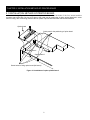
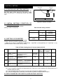
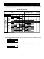
HITACHI INVERTER
SJ300/L300P SERIES
SJ-DG (DIGITAL INPUT OPTION)
INSTRUCTION MANUAL
Thank you for purchase of “HITACHI INVERTER”. This manual
explains about treatment of “SJ-DG (digital input option)”. By reading this
manual and an instruction manual of inverter use practically for
installation, maintenance, and inspection. After reading this manual, keep
it handy for future reference
Make sure to reach this manual to the end user.
Table of Contents
Chapter1
Chapter2
Chapter3
Chapter4
Chapter5
Introduction
Installation method of printed board
Wiring Connecting
Setting
Function
1
2
4
6
7
After reading this manual, keep it handy for future reference
NB617X
Request
Thank you for purchase of “HITACHI INVERTER”. This manual explains about handling of “SJ-DG (digital
input option)”.
This instruction manual explains about treatment and maintenance of “SJ-DG”. Before using the product,
carefully read this manual with the instruction manual of inverter, and keeps it handy for quick reference of
operator and maintenance inspector. Before installing, operating, maintenance and inspection read this manual
carefully and follow the instructions exactly.
Always keep various kinds of specification mentioned in this manual and use exactly. And make sure to
prevent trouble by correct inspection and maintenance. Make sure to reach this manual to the end user.
About treatment of this manual
Please consent that mentioned items of this manual may be change without permission.
Keep this manual carefully not to lose because it cannot be reissued.
All right reserved.
Contents in this manual is written to make assurance doubly sure but, but please contact if you have some
doubts about spelling mistakes, omitted word etc.
Please agree that there is no responsibility for effects resulted, in spite of contents above mentioned.
Revision History Table
No.
1.
Revision contents
Initial release
The date of issue
1999/12
Except this table, revised only spelling mistakes omitted words, and error writings without notice.
Manual No
NB617X
SAFETY PRECAUTIONS
SAFETY PRECAUTIONS
Carefully read this manual and all of the warning labels attached to the inverter before installing, operating,
maintaining, or inspecting it. Safety precautions are classified into “Warning” and “Caution” in this manual.
!
WARNING
: Indicates a potentially hazardous situation which, if not avoided, can result in serious injury or
death.
!
CAUTION
: Indicates a potentially hazardous situation which, if not avoided, can result in minor to moderate
injury, or serous damage to the product.
The situation described in WARNING may, if not avoided, lead to serious results. Important safety measures are
described in CAUTION (as well as WARNING) so be sure observe them.
Notes are described in this manual in “Note”, Precaution. Carefully read the contents and follow them exactly.
!
CAUTION
In all the illustrations in this manual, covers and safety devices are occasionally removed to describe the
details. When the product is operated, make sure that the covers and safety devices are placed as they were
specified originally and operate it according to the instruction manual.
SAFETY PRECAUTIONS
!
WARNING
Wiring:
• Wiring work shall be carried out by electrical experts
Otherwise, there is a danger of electric shock, fire and/or damage of product.
• Implement wiring after checking that the power supply is off.
Otherwise, there is a danger of electric shock and/or fire.
Operating:
• Be sure not to touch the surface or the terminal of option board while energizing.
Otherwise, there is a danger of electric shock and/or fire.
• Be sure not to remove the digital input option printed board while operating.
Otherwise, there is a danger of electric shock and/or fire.
Maintenance, Inspection and Part Replacement:
• Wait at least 10 minutes after turning off the input power supply before performing maintenance and
inspection.
(Confirm the charge lamp on the inverter is off, checks direct current voltage between P-N terminals and
confirm it is less than 45V.)
Otherwise, there is a danger of electric shock.
• Make sure that only qualified persons will perform maintenance, inspection, and part replacement
(Before starting the work, remove metallic objects from your person (wristwatch, bracelet, etc.).
Be sure to use tools protected with insulation)
Otherwise, there is a danger of electric shock, and/or injury.
Note:
• Never modify the unit.
Otherwise, there is a danger of electric shock and/or injury.
!
CAUTION
Installation:
• Be sure not to let the foreign matter enter such as wire clippings, spatter from welding, metal shaving,
dust, etc.
Otherwise, there is a danger of fire.
• Be sure to fix inverter to option printed board with an attached fixed screw.
Otherwise, there is a danger of connecting error.
• Be sure to fasten the screws connecting signal wire in side of option printed board. Check for any
loosening of screw.
Otherwise, there is a danger of connecting error.
Wiring:
• Be sure to fasten the screws not to loose.
Otherwise, there is a danger of connecting error.
Operation:
• Check rotary direction, abnormal motor noise and vibrations during operating.
Otherwise, there is a danger of injury to personnel and/or machine breakage.
SAFETY PRECAUTIONS
CHAPTER 1 INTRODUCTION
1.1 INSPECTION UPON UNPACKING
Make sure to treat the product carefully not to give shock and vibration while unpacking. Check that the product
is the one you ordered, and that there is no damage during transportation.
(Contents of packing)
(1) SJ-DG(digital input option printed board) : 1
(2) Instruction manual : 1
(3) Screws fixed printed board(M3 times 8mm) : 2
If you discover any problms, contact your sales agent immediately.
1.2 INQUIRY OF THE PRODUCT AND WARRANTY FOR THE PRODUCT
1.2.1 REQUIRE WHILE INQUIRING
If inquiry of breakage, question, damage etc. is needed, please tell the following information to the supplier you
ordered or the nearest Hitachi Distributor.
(1) Type
(2) Manufacturing number (MFG,NO)
(3) Day of purchasing
(4) Contents of inquiry
Damage part and its condition
Question parts and their contents etc.
In order to shorten impossible working time, standing spare unit is recommended.
1.2.2 WARRANTY OF THE PRODUCT
This product is guaranteed to last for one year after purchase. But, the next case is toll repair, even if within
warranty period.
(1)
(2)
(3)
(4)
In case caused by operating mistake, and incorrect repair and modification
Trouble caused by reasons except the shipped product.
In case of using in range over the value of specification.
In case caused by natural calamity, disaster, and secondary disaster,
Warranty mentioned here means warranty for shipped product itself. Damage caused by trouble of shipped
product is not guaranteed. Guarantee is valid only in Japan.
(Effective only Japan)
Toll repair
Any explanation and repair after the warranty period (one-year) shall be charged to the purchaser. And also any
explanation and repair out of warranty mentioned above, even within warranty period, shall be charged to the
purchaser. If you require the toll repair, please contact your Hitachi Distributor.
1.3 OUTLINE OF THE PRODUCT
If this option printed board is installed to SJ300/L300P series, it is possible to input setting frequency,
acceleration time setting, deceleration time setting, torque limit setting, and position setting in digital.
1
CHAPTER 2 INSTALLATION METHOD OF PRINTED BOARD
2.1 INSTALLATION METHOD OF PRINTED BOARD
As the following Figure 2-1, exactly connect option board 1 or 2 to the holes of the four corners and the
connector part of the back. Be sure to fit them to the guide post for positioning of option printed board and screw
holes for fixing. After connecting, fastened the two points of printed board with the fixed screws attached.
Option board
Guide post for the positioning of option board
Option board 1
Option board 2
Screw holes for fixing option board (M3 screw)
Figure 2-1 Installation of option printed board
2
CHAPTER 3 WIRING, CONNECTING
3.1 TERMINAL ASSIGNMENT OF DIGITAL INPUT OPTION BOARD
Figure 3-1a shows terminal assignment, Figure 3-1b shows terminal standard connection.
TM1
TM2
TM2
TM1 Terminal assignment
SEQ CMB D15 D14 D13 D12 D11 D10 D9
D8
D7
D6
D5
D4 D3
D2 D1
Terminal assignment
D0 STRBCM1 PLCB P24B
Figure 3-1a Terminal assignment
Inverter digital option printed board
RY
SEQ (Sequence error output terminal)
CMB (Common terminal)
D15
D14
(Data input signal)
D0
STRB (Strobe)
CM1 (Common terminal)
PLCB
(short circuit)
P24B
Figure 3-1b Terminal standard connection
In case of sink type interface, power is supplied to input terminal (D0 to D15, STRB) by short circuit between
P24B terminal and PLCB terminal.
3
CHAPTER 3 WIRING, CONNECTION
3.2 CONNECTION TO PROGRAMABLE CONTROLLER
In case of operating this unit connecting to programable controller, there are 4 patterns of input terminals (Table
3-2a), 2 patterns of output terminals(Table 3-2b). Please connect fitted to the type of programable controller used.
Table 3-2a Connection of Input terminal (Dn, STRB, CM1) to Programable controller
Sink logic
Source logic
In case of using internal interface power source
In case of using internal interface power source
P24B
COM
S
P24B
Short
Circuit
PLCB
DC24V
PLCB
Short
Circuit
DC24V
CM1
CM1
Dn
Dn
STRB
STRB
COM
S
YTR48 type
Output module
YTS48 type
Output module
SJ-DG
In case of using external power source
S
In case of using external power source
P24
COM
P24
PLC
B
CM1
SJ-DG
DC24
DC24
V
PLCB
DC24V
CM1
Dn
Dn
STRB
COM
STRB
DC24V
S
YTR48 type
Output module
SJ-DG
YTS48 type
Output module
SJ-DG
Table 3-2b Connection of output terminal(SEQ CMB) to programable controller
Sink logic
Source logic
4
CHAPTER 3 WIRING, CONNECTION
CMB
DC24V
COM
SEQ
DC24V
CMB
SJ-DG
SJ-DG
3.3 SPECIFICATION OF TERMINAL
Table 3-3 shows specification of terminal.
Table 3-3 Specification of terminal
Terminal
symbol
D15 to D0
Input
(Hereinafter
called as
Dn)
STRB
Terminal name
Data input terminal
Strobe terminal
(Data take in command
signal terminal)
Specification
Photo coupler input
(1a contact signal)
Sink source type
Sequence error signal
SEQ
(Data input error signal
output terminal)
Sink source type
CMB
Common terminal for
sequence error signal
output
Common
terminal
for
sequence error signal output
P24B
Power source terminal
for interface
DC24V power source for
contact input signal
In case of selecting source
logic, contact input common.
CM1
Power source terminal
for interface Common
terminal
Common terminal for data
input terminal, power source
for interface and strobe
Note)
terminal
Output
Power
source
Electric characteristics
Input impedance : 4.7k Ù
Allowable
Between SEQ and CMB
Voltage drop at on : less than 4V
Allowable max. voltage : DC27V
Allowable max. current : 50mA
Note)
Note) Never connect to earth of ground.
3.4 APPLICABLE WIRING
Make sure to use applicable wiring as the following items.
2.
wire that is shield
less than 0.5mm
Connect the wire which peeling length of sheathed signal wire is 5 –
In case of connecting twist wire, make sure not to loose
Use signal wire which max, outside diameter is less than 2.0mm2
5
Allowable max. current : 90mA
CHAPTER 4 SETTING
Dip switch
Rotary switch
CODE
4.1 POSITION OF SETTING SWITCH
TYPE
Figure 4-1shows position of setting switch.PAC, DIV,
BIN, BCD which printed around the dip switch (TYPE)
means one time input , 2 dividing input, binary input, BCD
input.
Figure 4-1 Position of switch
4.2 INITIAL SETTING CONDITION OF
PRINTED BOARD
Table 4-2 shows initial setting condition
(Setting condition at shipment).
Table 4-2 Initial setting condition
Setting item
4.3 SETTING OF INVERTER
Rotary switch
CODE
Switch No.
2
Initial setting
condition
PAC (OFF)
1
BIN (OFF)
0 to
0
Table 4-3 shows setting items of the inverter
(SJ300, L300 series) related to operating SJ-DG.
Make sure to refer to “CHAPTER 3 OPERATION”, “CHAPTER 4 EXPLANATION OF FUNCTION” of the
instruction manual of the inverter, and set exactly.
Table 4-3 Table of setting items of inverter related to SJ-DG
Code
Function name
Data range
Initial data
Possible
setting at
operating
Possible mode
of change at
operating
Note
A001
Setting frequency
destination
00(VR)/01(terminal)/02(operator)
/03(RS485)/04(option1)
/05(option2)
02 (SJ300)
00 (L300P)
X
X
-
P031
One selection of
acceleration
and
deceleration time
00(remote)/01(option1)
/02(option2)
00
X
O
-
B040
Selection of torque
limit
00(4quadrant individual setting)
/01(terminal
switch)/02(analog
input)/03(option1)/04(option 2)
00
X
O
Only
SJ300
P032
Selection
of
position command
00(remote)/01(option1)
/02(option2)
00
X
O
Only
SJ300
(1) In case of setting frequency, make sure to set frequency command destination (A001) to option.
(2) In case of setting acceleration and deceleration time, make sure to set acceleration and deceleration time 1
selection (P031) to option.
(3) In case of setting torque limit, make sure to set torque limit selection (B040) to option.
(4) In case of setting position, make sure to set selection of position command (P032) to option.
4.4 INPUT MODE BY DIP SWITCH AND ROTARY SWITCH
6
CHAPTER 4 SETTING
It is possible to select input mode by combination of dip switch and rotary switch on the option printed board.
Table 4-4 shows table of input mode.
Table 4-4 Table of input mode
Dip switch
TYPE
Switch No.
1
2
Rotary
switch
Acceleration and
deceleration time setting
Setting frequency
CODE
Torque
limit
setting
Position
setting
Setting resolution
Setting
0.01Hz 0.1Hz
1Hz
Rate
0.01sec 0.1sec
1sec
1%
1pulse
code
0
O
PAC
1
O
(One
2
O
time
3
O
input
4
O
mode at
5
BIN
OFF)
6
O
(Binary
0
O
input at
1
O
O
OFF)
2
O
/
3
O
BCD
DIV
4
O
O
(BCD
(Dividing
5
O
input at
input
O
O
6
O
ON)
mode at
7
O
O
ON)
8
O
9
O
O
A
O
B
O
Precaution O shows input mode set by switch setting. Make sure not to set switch setting except O because they are for
adjustments of factory.
(Viewpoint of table of input mode)
Example 1) In one time input mode, switch setting which sets setting frequency by 1Hz resolution and binary
input.
TYPE
CODE
1
2
2
BIN
PAC
Example 2) In two dividing input, switch setting which sets setting frequency with 0.1Hz resolution and BCD
input, and in case of setting acceleration and deceleration time by BCD input, 0.1sec.resolution.
TYPE
CODE
1
2
2
BCD
DIV
7
CHAPTER 4 SETTING
4.5 PRECAUTIONS AT SETTING OF SWITCH
(1) In case of setting rotary switch code to (5, 7 to F) in one time input mode, sequence error outputs just after
power on of inverter.
(2) In case of setting rotary switch code to (B to F) in 2 dividing input mode, sequence error outputs just after
power on of inverter.
(3) In case of (1) or (2), turn off power of inverter and set exactly.
8
CHAPTER 5 FUNCTION
5.1 FUNCTION
5.1.1 ONE TIME BINARY INPUT
Setting of dip switch TYPE
It is possible to select frequency setting, torque limit setting or
position setting of one time data input by rotary switch CODE.
Figure 5.1.1shows data bit construction of one time binary input.
(Example of setting) In case of setting frequency to 60.0Hz by 0.1Hz
resolution
1
2
BIN
PAC
(Lower)
(Higher)
D15
D14
D13
D12
D11
D10
D9
D8
D7
D6
D5
D4
D3
D2
D1
D0
Setting
Figure 5.1.1 Data bit construction of one time binary input
(Setting of rotary switch CODE --- 1).
(1) Input value which 60 multiplies 10 to D15 - D0 terminal by 16 bits binary value.
D15
D14
D13
D12
D11
D10
D9
D8
D7
D6
D5
D4
D3
D2
D1
D0
0
0
0
0
0
0
1
0
0
1
0
1
1
0
0
0
16 bits data
(1) 60 times10 = 600 ---- 0000001001011000 (Binary)
(2) When data input is definite, turn the strobe signal on.
(3) Turn the strobe signal off.
Precaution Refer to 5.3 ”DATA INPUT TIMING” for signal input timing.
5.1.2 ONE TIME BCD INPUT
Setting of dip switch TYPE
1
2
It is possible to select frequency setting, torque limit setting or position
setting of one time data input by rotary switch CODE.
Figure 5.1.2 shows data bit construction of one time BCD input.
(Example of setting) In case of setting frequency to 30.0Hz resolution by
0.01Hz
(Setting of rotary switch CODE ---- 1)
BCD
PAC
(1) Input value which 30 multiplies 100 to D15 to D0 terminal by BCD value.
30 times100 = 3000 ---- 0011000000000000 (binary)
(Lower)
(Higher)
D15
D14
D13
Setting data 4
D12
D11
D10
D9
D8
D7
Setting data 3
D6
D5
Setting data 2
D4
D3
D2
Setting data 1
Figure 5.1.2 Data bit construction of one time BCD input
(2) When data input is definite, turn the strobe signal on.
(3) Turn the strobe signal off.
9
D1
D0
CHAPTER 5 FUNCTION
D15
D14
D13
D12
D11
D10
D9
D8
D7
D6
D5
D4
D3
D2
D1
D0
0
0
1
1
0
0
0
0
0
0
0
0
0
0
0
0
Setting data 4
Setting data 3
Setting data 2
Setting data 1
Precaution Refer to 5.3 ”DATA INPUT TIMING” for signal input timing.
5.1.3 TWO DIVIDING BINARY INPUT
Setting of dip switch TYPE
It is possible to change setting data by twice input of data, higher data
1
2
and lower data. And it is possible to select frequency setting, torque limit
BIN
DIV
setting, acceleration and deceleration time setting or position setting by
change of classification code (Refer to Figure 5.2 Table of classification
code.). Setting resolution can be selected by rotary switch CODE.
Figure 5.1.3 shows data bit construction of the input binary data divided into two.
(Lower)
(Higher)
D15
D14
D13
D12
D11
D10
D9
D8
D7
D6
D5
D4
D3
D2
D1
D0
Setting data of higher 8bits or lower 8 bints
Higher or Lower classification code
Figure 5.1.3 Data bit construction of the input binary data divided into two
(Example of setting) In case of setting frequency to resolution 0.01Hz
(Setting of rotary switch CODE --- 0, 1, 2
(1) Converse value which 60 multiply 100 to 16 bits binary value. And then input higher 8 bits to D7 to D0
terminal, higher code of setting frequency to D15 to D8 terminal.
60×100 = 6000
0001011101110000 (Binary)
D15
D14
D13
D12
D11
D10
D9
D8
D7
D6
D5
D4
D3
D2
D1
D0
0
0
0
0
0
0
0
0
0
1
0
1
0
1
1
1
Higher 8 bits setting data
Higher code setting frequency
(2) When data input is definite, turn strobe signal on.
(3) Turn strobe signal off.
(4) Input remaining data, lower 8 bits to D7 to D0 terminal, and D15 to D8terminal to lower code of setting
D15
D14
D13
D12
D11
D10
D9
D8
D7
D6
D5
D4
D3
D2
D1
D0
0
0
0
0
0
0
0
1
0
1
1
1
0
0
0
0
Lower 8 bits setting data
Lower code setting frequency
frequency.
(5) When data input is definite, turn strobe signal on.
(6) Turn strobe signal off.
Precaution Refer to 5.3 ”DATA INPUT TIMING” for signal input timing.
10
CHAPTER 5 FUNCTION
5.1.4 TWO DIVIDING BCD INPUT
Setting of dip switch TYPE
It is possible to change setting data by twice input of data, higher data
1
2
and lower data. And it is possible to select frequency setting, torque limit
setting, acceleration and deceleration time setting, or position setting by
BCD
DIV
change of classification code (Refer to Figure 5.2 Table of classification
code.). Setting resolution can be selected by rotary switch CODE.
(Example of setting) In case of setting acceleration time to 60.0sec by 0.1sec resolution
D15
D14
D13
D12
D11
D10
D9
D8
D7
D6
D5
D4
D3
D2
D1
D0
0
0
0
0
0
0
0
1
0
1
1
1
0
0
0
0
Lower 8 bits setting data
Lower code setting frequency
Figure 5.1.4 Data bit construction of the input BCD data divided into two
(Setting of rotary switch CODE ---- 1, 4, 7, A)
(1) Converse value which 60 multiply 10 to binary value of BCD. And then input higher 2-figure data to D7 to
D0 terminal, acceleration time setting higher code to D15 to D8 terminal.
60×10 = 600
0000011000000000 (Binary)
D15
D14
D13
D12
D11
D10
D9
D8
D7
D6
D5
D4
D3
D2
D1
D0
0
0
0
0
0
1
0
0
0
0
0
0
0
1
1
0
Higher 2-figure setting data
Acceleration time setting higher code
(2) When data input is definite, turn the strobe signal on.
(3) Turn the strobe signal off.
(4) Input remaining data, lower 8 bits to D7 to D0 terminal, and D15 to D8 terminal to lower code of setting
frequency.
D15
D14
D13
D12
D11
D10
D9
D8
D7
D6
D5
D4
D3
D2
D1
D0
0
0
0
0
0
1
0
1
0
0
0
0
0
0
0
0
Acceleration time setting lower code
(5) When data input is definite, turn the strobe signal on.
(6) Turn strobe signal off.
Precaution Refer to 5.3 ”DATA INPUT TIMING” for signal input timing.
11
Lower 2-figure setting data
CHAPTER 5 FUNCTION
5.2 CLASSIFICATION CODE
Table 5.2 shows table of classification
code. Make sure to input classification code
in order, higher code and then lower code.
Table 5.2 Table of classification code
Classification code
Setting item
5.3 DATA INPUT TIMING
5.3.1 TIMING AT ONE TIME INPUT
MO
DE
Setting frequency (Higher)
(D15 - D8)
Binary
Hexadecimal
00000000
0
Setting frequency (Lower)
00000001
1
Torque limit setting (Higher)
00000010
2
Torque limit setting (Lower)
00000011
3
Acceleration time setting (Higher)
00000100
4
Acceleration time setting (Lower)
00000101
5
Deceleration time setting(Higher)
00000110
6
Deceleration time setting(Lower)
00000111
7
Position setting (Higher)
00001000
8
Position setting (Lower)
00001001
9
Take in data in on level that strobe signal. Let on/off time of strobe signal be more than 20ms. Be in state of on.
And if data indefinite area is more than 5ms, turn strobe signal off in order to satisfy Figure 5.3.1 timing chart of one
time data input.
Data indefinite
period
within 5ms
Data indefinite
period
within 5ms
Data definite
period
more than 20ms
Dn
(n=0-15)
Normal data
Data indefinite
period
within 5ms
Data definite
period
more than 20ms
Data definite
period
more than 20ms
Data definite
period
more than 20ms
Abnormal data
Normal data
Normal data
More than 20ms
More than 0ms
More than 0ms
ON
ON
STRB
OFF
OFF
More than 20ms
SEQ
(Sequence error output)
More than 20ms
ON
OFF
OFF
Within 20ms
Within 20ms
At load current 20mA
Precaution If Figure 5.3.1 timing chart is not satisfied, be careful because of possibility of taking in error
data.
12
CHAPTER 5 FUNCTION
5.3.2 TIMING AT TWO DIVIDING DATA INPUT
Take in data in on-edge of strove signal. Let on/off time of strobe signal be more than 20ms. And let off time of
strobe signal be more than 20ms,
Data definite
period
Dn
(n=0-15)
Data definite
period
Data definite
period
Normal data
Abnormal data
Normal data
More than 0ms
More than 0ms
More than 0ms
ON
ON
ON
STRB
OFF
OFF
More than
20ms
OFF
More than
20ms
More than
20ms
More than
20ms
OFF
More than
20ms
ON
SEQ
(Sequence error output)
OFF
OFF
Within 20ms
Within 20ms
At load current 20mA
Figure 5.3.2 Timing chart of two dividing data input
Precaution If Figure 5.3.2 timing chart is not satisfied, be careful because of possibility of taking in error
data.
5.4 NOTICE AT DATA INPUT
While inputting the data by terminal of SJ-DG, notice the following items.
(1) Each input is possible to set within data range of the inverter in every setting item. If inputting without data
range, sequence error is outputted and data input is invalid (previous data is kept).
(2) If classification code is inputted in dividing input mode, make sure to input classification code in order, higher
code, and then lower code. If lower code is inputted at first, sequence error is outputted and data input is
invalid (previous data is kept)
(3) Re-input of correct data, or reset of inverter, or power off carries out cancellation of sequence error. And, if
two times input are correct in dividing input mode, they are cancelled just after second input.
(4) If a code without codes in table of classification is inputted, sequence error is outputted.
(5) In case of trip of inverter, data input is invalid. Make sure to reset inverter and re-input.
(6) When each command destination of inverter is not set to option board put on, do not input data.
(7) If setting frequency is input in “rate”, do the following process below.
(Example) If 75% of max frequency is set, input I in is
I in = 0.75 × M
0.75 rate
M input data full scale
Input data full scale value( M )
65535
Switch type 1
BIN
13
CHAPTER 5 FUNCTION
BCD
9999
However, f Hz set actually is calculated in
f =
I in
Fmax
M
Fmax
max frequency Hz
and, value which is ignored less than is setting frequency.
14