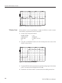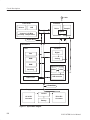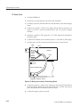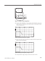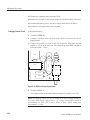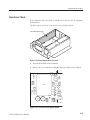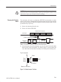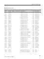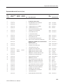
1
Service Manual 1502C Metallic Time-Domain Reflectometer 070-7168-04 This document applies to firmware version 5.02 and above. Warning The servicing instructions are for use by qualified personnel only. To avoid personal injury, do not perform any servicing unless you are qualified to do so. Refer to all safety summaries prior to performing service. www.tektronix.com Copyright © Tektronix, Inc. All rights reserved. Tektronix products are covered by U.S. and foreign patents, issued and pending. Information in this publication supercedes that in all previously published material. Specifications and price change privileges reserved. Tektronix, Inc., P.O. Box 500, Beaverton, OR 97077 TEKTRONIX and TEK are registered trademarks of Tektronix, Inc. WARRANTY Tektronix warrants that the products that it manufactures and sells will be free from defects in materials and workmanship for a period of one (1) year from the date of shipment. If a product proves defective during this warranty period, Tektronix, at its option, either will repair the defective product without charge for parts and labor, or will provide a replacement in exchange for the defective product. In order to obtain service under this warranty, Customer must notify Tektronix of the defect before the expiration of the warranty period and make suitable arrangements for the performance of service. Customer shall be responsible for packaging and shipping the defective product to the service center designated by Tektronix, with shipping charges prepaid. Tektronix shall pay for the return of the product to Customer if the shipment is to a location within the country in which the Tektronix service center is located. Customer shall be responsible for paying all shipping charges, duties, taxes, and any other charges for products returned to any other locations. This warranty shall not apply to any defect, failure or damage caused by improper use or improper or inadequate maintenance and care. Tektronix shall not be obligated to furnish service under this warranty a) to repair damage resulting from attempts by personnel other than Tektronix representatives to install, repair or service the product; b) to repair damage resulting from improper use or connection to incompatible equipment; c) to repair any damage or malfunction caused by the use of non-Tektronix supplies; or d) to service a product that has been modified or integrated with other products when the effect of such modification or integration increases the time or difficulty of servicing the product. THIS WARRANTY IS GIVEN BY TEKTRONIX IN LIEU OF ANY OTHER WARRANTIES, EXPRESS OR IMPLIED. TEKTRONIX AND ITS VENDORS DISCLAIM ANY IMPLIED WARRANTIES OF MERCHANTABILITY OR FITNESS FOR A PARTICULAR PURPOSE. TEKTRONIX’ RESPONSIBILITY TO REPAIR OR REPLACE DEFECTIVE PRODUCTS IS THE SOLE AND EXCLUSIVE REMEDY PROVIDED TO THE CUSTOMER FOR BREACH OF THIS WARRANTY. TEKTRONIX AND ITS VENDORS WILL NOT BE LIABLE FOR ANY INDIRECT, SPECIAL, INCIDENTAL, OR CONSEQUENTIAL DAMAGES IRRESPECTIVE OF WHETHER TEKTRONIX OR THE VENDOR HAS ADVANCE NOTICE OF THE POSSIBILITY OF SUCH DAMAGES. Table of Contents General Safety Summary . . . . . . . . . . . . . . . . . . . . . . . . . . . . . . . . . . . . . . . . . . . Service Safety Summary . . . . . . . . . . . . . . . . . . . . . . . . . . . . . . . . . . . . . . . . . . . General Information . . . . . . . . . . . . . . . . . . . . . . . . . . . . . . . . . . . . . . . . xi xiii xv Installation and Repacking . . . . . . . . . . . . . . . . . . . . . . . . . . . . . . . . . . . . . . . . . . Contacting Tektronix . . . . . . . . . . . . . . . . . . . . . . . . . . . . . . . . . . . . . . . . . . . . . . xvi xviii Operating Instructions . . . . . . . . . . . . . . . . . . . . . . . . . . . . . . . . . . . . . . 1–1 Overview . . . . . . . . . . . . . . . . . . . . . . . . . . . . . . . . . . . . . . . . . . . . . . . . . . . . . . . Preparing to Use the 1502C . . . . . . . . . . . . . . . . . . . . . . . . . . . . . . . . . . . . . . . . . Display . . . . . . . . . . . . . . . . . . . . . . . . . . . . . . . . . . . . . . . . . . . . . . . . . . . . . . . . . Front-Panel Controls . . . . . . . . . . . . . . . . . . . . . . . . . . . . . . . . . . . . . . . . . . . . . . Menu Selections . . . . . . . . . . . . . . . . . . . . . . . . . . . . . . . . . . . . . . . . . . . . . . . . . . Test Preparations . . . . . . . . . . . . . . . . . . . . . . . . . . . . . . . . . . . . . . . . . . . . . . . . . Cable Test Procedure . . . . . . . . . . . . . . . . . . . . . . . . . . . . . . . . . . . . . . . . . . . . . . Additional Features (Menu Selected) . . . . . . . . . . . . . . . . . . . . . . . . . . . . . . . . . . 1–1 1–5 1–6 1–6 1–7 1–11 1–13 1–26 Operating Instructions Operator Performance Checks Operator Performance Checks . . . . . . . . . . . . . . . . . . . . . . . . . . . . . . . 2–1 Specifications . . . . . . . . . . . . . . . . . . . . . . . . . . . . . . . . . . . . . . . . . . . . . . 3–1 Electrical Characteristics . . . . . . . . . . . . . . . . . . . . . . . . . . . . . . . . . . . . . . . . . . . Environmental Characteristics . . . . . . . . . . . . . . . . . . . . . . . . . . . . . . . . . . . . . . . Certifications and Compliances . . . . . . . . . . . . . . . . . . . . . . . . . . . . . . . . . . . . . . Physical Characteristics . . . . . . . . . . . . . . . . . . . . . . . . . . . . . . . . . . . . . . . . . . . . 3–1 3–3 3–4 3–5 Specifications Options and Accessories Options and Accessories . . . . . . . . . . . . . . . . . . . . . . . . . . . . . . . . . . . . . 4–1 Option 04: YT–1 Chart Recorder . . . . . . . . . . . . . . . . . . . . . . . . . . . . . . . . . . . . . Option 05: Metric Default . . . . . . . . . . . . . . . . . . . . . . . . . . . . . . . . . . . . . . . . . . Option 07: YT–1S Chart Recorder . . . . . . . . . . . . . . . . . . . . . . . . . . . . . . . . . . . Power Cord Options . . . . . . . . . . . . . . . . . . . . . . . . . . . . . . . . . . . . . . . . . . . . . . . Accessories . . . . . . . . . . . . . . . . . . . . . . . . . . . . . . . . . . . . . . . . . . . . . . . . . . . . . . 4–1 4–1 4–1 4–1 4–2 Circuit Descriptions . . . . . . . . . . . . . . . . . . . . . . . . . . . . . . . . . . . . . . . . . 5–1 Introduction . . . . . . . . . . . . . . . . . . . . . . . . . . . . . . . . . . . . . . . . . . . . . . . . . . . . . Power Supply . . . . . . . . . . . . . . . . . . . . . . . . . . . . . . . . . . . . . . . . . . . . . . . . . . . . 5–1 5–4 Circuit Descriptions 1502C MTDR Service Manual i Table of Contents Processor System . . . . . . . . . . . . . . . . . . . . . . . . . . . . . . . . . . . . . . . . . . . . . . . . . Option Port Interface . . . . . . . . . . . . . . . . . . . . . . . . . . . . . . . . . . . . . . . . . . . . . . Video Processor . . . . . . . . . . . . . . . . . . . . . . . . . . . . . . . . . . . . . . . . . . . . . . . . . . Timebase . . . . . . . . . . . . . . . . . . . . . . . . . . . . . . . . . . . . . . . . . . . . . . . . . . . . . . . Driver/Sampler . . . . . . . . . . . . . . . . . . . . . . . . . . . . . . . . . . . . . . . . . . . . . . . . . . . Front Panel . . . . . . . . . . . . . . . . . . . . . . . . . . . . . . . . . . . . . . . . . . . . . . . . . . . . . . Display Module . . . . . . . . . . . . . . . . . . . . . . . . . . . . . . . . . . . . . . . . . . . . . . . . . . 5–7 5–10 5–13 5–15 5–23 5–25 5–28 Calibration and Adjustments Calibration . . . . . . . . . . . . . . . . . . . . . . . . . . . . . . . . . . . . . . . . . . . . . . . . 6–1 Introduction . . . . . . . . . . . . . . . . . . . . . . . . . . . . . . . . . . . . . . . . . . . . . . . . . . . . . 6–1 Calibration Performance Check . . . . . . . . . . . . . . . . . . . . . . . . . . . . . . 6–1 Display Module Check . . . . . . . . . . . . . . . . . . . . . . . . . . . . . . . . . . . . . . . . . . . . . Front Panel Check . . . . . . . . . . . . . . . . . . . . . . . . . . . . . . . . . . . . . . . . . . . . . . . . Horizontal Scale (Timebase) Check . . . . . . . . . . . . . . . . . . . . . . . . . . . . . . . . . . . Zero Offset Check . . . . . . . . . . . . . . . . . . . . . . . . . . . . . . . . . . . . . . . . . . . . . . . . Vertical Position (Offset) Check . . . . . . . . . . . . . . . . . . . . . . . . . . . . . . . . . . . . . Noise Check . . . . . . . . . . . . . . . . . . . . . . . . . . . . . . . . . . . . . . . . . . . . . . . . . . . . . Sampling Efficiency Check . . . . . . . . . . . . . . . . . . . . . . . . . . . . . . . . . . . . . . . . . Offset/Gain Check . . . . . . . . . . . . . . . . . . . . . . . . . . . . . . . . . . . . . . . . . . . . . . . . RAM/ROM Check . . . . . . . . . . . . . . . . . . . . . . . . . . . . . . . . . . . . . . . . . . . . . . . . Aberrations Check . . . . . . . . . . . . . . . . . . . . . . . . . . . . . . . . . . . . . . . . . . . . . . . . Risetime Check . . . . . . . . . . . . . . . . . . . . . . . . . . . . . . . . . . . . . . . . . . . . . . . . . . Jitter Check . . . . . . . . . . . . . . . . . . . . . . . . . . . . . . . . . . . . . . . . . . . . . . . . . . . . . . Option 04/07: YT-1/YT-1S Chart Recorder Check . . . . . . . . . . . . . . . . . . . . . . . Option 05: Metric Default Check . . . . . . . . . . . . . . . . . . . . . . . . . . . . . . . . . . . . . 6–2 6–4 6–7 6–10 6–12 6–13 6–15 6–16 6–17 6–17 6–19 6–21 6–23 6–23 Adjustment Procedures . . . . . . . . . . . . . . . . . . . . . . . . . . . . . . . . . . . . . . 6–25 Visual Inspection . . . . . . . . . . . . . . . . . . . . . . . . . . . . . . . . . . . . . . . . . . . . . . . . . Power Supply Checks and Adjustments . . . . . . . . . . . . . . . . . . . . . . . . . . . . . . . Main Board ”12 VDC Check and Adjust . . . . . . . . . . . . . . . . . . . . . . . . . . . . . . . Impedance Check . . . . . . . . . . . . . . . . . . . . . . . . . . . . . . . . . . . . . . . . . . . . . . . . . LCD Check and Adjustment . . . . . . . . . . . . . . . . . . . . . . . . . . . . . . . . . . . . . . . . Zero Offset Adjust . . . . . . . . . . . . . . . . . . . . . . . . . . . . . . . . . . . . . . . . . . . . . . . . After Adjustments are Completed . . . . . . . . . . . . . . . . . . . . . . . . . . . . . . . . . . . . 6–26 6–26 6–30 6–35 6–36 6–39 6–41 Maintenance . . . . . . . . . . . . . . . . . . . . . . . . . . . . . . . . . . . . . . . . . . . . . . . 7–1 Introduction . . . . . . . . . . . . . . . . . . . . . . . . . . . . . . . . . . . . . . . . . . . . . . . . . . . . . Preventive Maintenance . . . . . . . . . . . . . . . . . . . . . . . . . . . . . . . . . . . . . . . . . . . . Part Removal and Replacement . . . . . . . . . . . . . . . . . . . . . . . . . . . . . . . . . . . . . . Troubleshooting . . . . . . . . . . . . . . . . . . . . . . . . . . . . . . . . . . . . . . . . . . . . . . . . . . Control Panel Installation . . . . . . . . . . . . . . . . . . . . . . . . . . . . . . . . . . . . . . . . . . . Installing the Case Cover Over the Chassis . . . . . . . . . . . . . . . . . . . . . . . . . . . . . 7–1 7–1 7–2 7–12 7–17 7–19 Maintenance ii 1502C MTDR Service Manual Table of Contents Replaceable Electrical Parts Replaceable Electrical Parts . . . . . . . . . . . . . . . . . . . . . . . . . . . . . . . . . . 8–1 Parts Ordering Information . . . . . . . . . . . . . . . . . . . . . . . . . . . . . . . . . . . . . . . . . 8–1 Diagrams . . . . . . . . . . . . . . . . . . . . . . . . . . . . . . . . . . . . . . . . . . . . . . . . . 9–1 General Information . . . . . . . . . . . . . . . . . . . . . . . . . . . . . . . . . . . . . . . . . . . . . . . 9–1 Diagrams Replaceable Mechanical Parts Replaceable Mechanical Parts . . . . . . . . . . . . . . . . . . . . . . . . . . . . . . . . 10–1 Parts Ordering Information . . . . . . . . . . . . . . . . . . . . . . . . . . . . . . . . . . . . . . . . . Using the Replaceable Mechanical Parts List . . . . . . . . . . . . . . . . . . . . . . . . . . . 10–1 10–1 Glossary and Index 1502C MTDR Service Manual iii Table of Contents List of Figures Figure 1–1: Figure 1–2: Figure 1–3: Figure 1–4: Figure 1–5: Figure 1–6: Figure 1–7: Figure 1–8: Figure 1–9: Figure 1–10: Figure 1–11: Figure 1–12: Figure 1–13: Figure 1–14: Figure 1–15: Figure 1–16: Figure 1–17: Figure 1–18: Figure 1–19: Figure 1–20: Figure 1–21: Figure 1–22: Figure 1–23: Figure 1–24: Figure 1–25: Figure 1–26: Figure 1–27: Figure 1–28: Figure 1–29: Figure 1–30: Figure 1–31: Figure 1–32: Figure 1–33: iv Rear Panel Voltage Selector, Fuse, AC Receptacle . . . . . Display Showing Low Battery Indication . . . . . . . . . . . . 1502C Front-Panel Controls . . . . . . . . . . . . . . . . . . . . . . Display and Indicators . . . . . . . . . . . . . . . . . . . . . . . . . . . Vp Set at .30, Cursor Beyond Reflected Pulse (Set Too Low) . . . . . . . . . . . . . . . . . . . . . . . . . . . . . . . . . Vp Set at .99, Cursor Less Than Reflected Pulse (Set Too High) . . . . . . . . . . . . . . . . . . . . . . . . . . . . . . . . . Vp Set at .66, Cursor at Reflected Pulse (Set Correctly) 20-ft Cable at 5 ft/div . . . . . . . . . . . . . . . . . . . . . . . . . . . Short in the Cable . . . . . . . . . . . . . . . . . . . . . . . . . . . . . . Open in the Cable . . . . . . . . . . . . . . . . . . . . . . . . . . . . . . 455-ft Cable . . . . . . . . . . . . . . . . . . . . . . . . . . . . . . . . . . . 455-ft Cable . . . . . . . . . . . . . . . . . . . . . . . . . . . . . . . . . . . Reflection Adjusted to One Division in Height . . . . . . . Return Loss . . . . . . . . . . . . . . . . . . . . . . . . . . . . . . . . . . . Ohms-at-Cursor . . . . . . . . . . . . . . . . . . . . . . . . . . . . . . . . Display with VIEW INPUT Turned Off . . . . . . . . . . . . . Display of a Stored Waveform . . . . . . . . . . . . . . . . . . . . Display of a Stored Waveform . . . . . . . . . . . . . . . . . . . . Waveform Moved to Top Half of Display . . . . . . . . . . . . Current Waveform Centered, Stored Waveform Above . Current Waveform Center, Stored Waveform Above, Difference Below . . . . . . . . . . . . . . . . . . . . . . . . . . . . . . Waveform of Three-Foot Lead-in Cable . . . . . . . . . . . . . Cursor Moved to End of Three-Foot Lead-in Cable . . . . Cursor Moved to End of Three-Foot Lead-in Cable . . . . Cursor Moved to 0.00 ft . . . . . . . . . . . . . . . . . . . . . . . . . Incident Pulse at Three Divisions . . . . . . . . . . . . . . . . . . Waveform of Short 75W Cable . . . . . . . . . . . . . . . . . . . . Waveform Centered and Adjusted Vertically . . . . . . . . . Cursor Moved to Desired Position . . . . . . . . . . . . . . . . . Waveform Viewed in Normal Operation . . . . . . . . . . . . . Waveform Showing Intermittent Changes . . . . . . . . . . . Waveform Display with No Outgoing Pulses . . . . . . . . . A Captured Single Sweep . . . . . . . . . . . . . . . . . . . . . . . . 1–1 1–4 1–5 1–6 1–12 1–12 1–12 1–13 1–13 1–14 1–14 1–15 1–15 1–17 1–17 1–18 1–19 1–19 1–20 1–20 1–21 1–22 1–22 1–23 1–23 1–24 1–24 1–25 1–25 1–26 1–27 1–27 1–29 1502C MTDR Service Manual Table of Contents Figure 2–1: Figure 2–2: Figure 2–3: Figure 2–4: Figure 2–5: Figure 2–6: Figure 2–7: Figure 2–8: Figure 2–9: Figure 2–10: Figure 2–15: Figure 2–16: Start-up Measurement Display . . . . . . . . . . . . . . . . . . . . Measurement Display with 3-foot Cable . . . . . . . . . . . . Cursor at End of 3-foot Cable . . . . . . . . . . . . . . . . . . . . . Flat-Line Display Out to 50,000+ Feet . . . . . . . . . . . . . . Flat-Line Display at –2.000 ft . . . . . . . . . . . . . . . . . . . . . Waveform Off the Top of the Display . . . . . . . . . . . . . . . Waveform at the Bottom of the Display . . . . . . . . . . . . . Waveform with Gain at 5.00 mr/div . . . . . . . . . . . . . . . Top of Pulse on Center Graticule . . . . . . . . . . . . . . . . . . Rising Edge of Incident Pulse in Left-most Major Division . . . . . . . . . . . . . . . . . . . . . . . . . . . . . . . . Waveform Centered, Cursor at 0.000 ft . . . . . . . . . . . . . Pulse Centered on Display . . . . . . . . . . . . . . . . . . . . . . . Cursor on Lowest Major Graticule that Rising Edge Crosses . . . . . . . . . . . . . . . . . . . . . . . . . . . . . . . . . . Cursor on Highest Major Graticule that Rising Edge Crosses . . . . . . . . . . . . . . . . . . . . . . . . . . . . . . . . . . Jitter Apparent on Leading Edge of Incident Pulse . . . . Jitter Captured Using Max Hold . . . . . . . . . . . . . . . . . . . 2–9 2–10 2–10 Figure 5–1: Figure 5–2: Figure 5–3: Figure 5–4: Figure 5–5: Figure 5–6: Figure 5–7: Figure 5–8: Figure 5–9: Figure 5–10: Figure 5–11: Figure 5–12: Figure 5–13: Figure 5–14: Figure 5–15: Figure 5–16: Figure 5–17: Figure 5–18: Figure 5–19: System Block Diagram . . . . . . . . . . . . . . . . . . . . . . . . . . Waveform Accumulation Diagram . . . . . . . . . . . . . . . . . Power Supply Block Diagram . . . . . . . . . . . . . . . . . . . . . Processor Block Diagram . . . . . . . . . . . . . . . . . . . . . . . . Option Port Interface Block Diagram . . . . . . . . . . . . . . . Video Processor Block Diagram . . . . . . . . . . . . . . . . . . . Video Processor Output . . . . . . . . . . . . . . . . . . . . . . . . . . Timebase Block Diagram . . . . . . . . . . . . . . . . . . . . . . . . Timebase Control . . . . . . . . . . . . . . . . . . . . . . . . . . . . . . Combined Effects of Time Delay . . . . . . . . . . . . . . . . . . Calibration of Delay Zero and 50-ns Analog Delay . . . . Driver/Sampler Block Diagram . . . . . . . . . . . . . . . . . . . Front Panel Block Diagram . . . . . . . . . . . . . . . . . . . . . . . Display Module Block Diagram . . . . . . . . . . . . . . . . . . . SBE Cell . . . . . . . . . . . . . . . . . . . . . . . . . . . . . . . . . . . . . Row Driver Block Diagram . . . . . . . . . . . . . . . . . . . . . . Column Driver Block Diagram . . . . . . . . . . . . . . . . . . . . Row Timing Diagram . . . . . . . . . . . . . . . . . . . . . . . . . . . Column Timing Diagram . . . . . . . . . . . . . . . . . . . . . . . . 5–2 5–3 5–4 5–8 5–11 5–13 5–15 5–16 5–17 5–18 5–19 5–24 5–26 5–29 5–30 5–31 5–32 5–33 5–35 Figure 2–11: Figure 2–12: Figure 2–13: Figure 2–14: 1502C MTDR Service Manual 2–2 2–2 2–3 2–3 2–4 2–4 2–5 2–5 2–7 2–7 2–8 2–8 2–9 v Table of Contents vi Figure 5–20: Figure 5–21: Shift Register . . . . . . . . . . . . . . . . . . . . . . . . . . . . . . . . . . CPU and Display Memory Interface . . . . . . . . . . . . . . . . 5–36 5–39 Figure 6–1: Figure 6–2: Figure 6–3: Figure 6–4: Figure 6–5: Figure 6–6: Figure 6–7: Figure 6–8: Figure 6–9: Figure 6–10: Figure 6–11: Figure 6–12: Figure 6–13: Figure 6–14: Figure 6–15: Figure 6–16: Figure 6–17: Figure 6–18: Figure 6–19: Figure 6–20: Figure 6–21: Figure 6–22: Figure 6–23: Figure 6–24: Figure 6–25: Figure 6–26: Figure 6–27: Figure 6–28: Figure 6–29: Figure 6–30: Figure 6–31: Figure 6–32: Figure 6–33: Figure 6–34: Figure 6–35: Figure 6–36: Typical Start-Up Display . . . . . . . . . . . . . . . . . . . . . . . . . Waveform on the Display . . . . . . . . . . . . . . . . . . . . . . . . Setup Menu . . . . . . . . . . . . . . . . . . . . . . . . . . . . . . . . . . . Main Menu . . . . . . . . . . . . . . . . . . . . . . . . . . . . . . . . . . . Diagnostics Menu . . . . . . . . . . . . . . . . . . . . . . . . . . . . . . Front Panel Diagnostic Display . . . . . . . . . . . . . . . . . . . . Front Panel Diagnostic Display . . . . . . . . . . . . . . . . . . . . Front Panel Diagnostic Display . . . . . . . . . . . . . . . . . . . . Front Panel Diagnostic Display . . . . . . . . . . . . . . . . . . . . Waveform on the Display with No Cable Attached . . . . Display with 3-ft Cable and Stored Waveform . . . . . . . . Cursor on Rising Edge of Pulse . . . . . . . . . . . . . . . . . . . Cursor at 0.000 ft n . . . . . . . . . . . . . . . . . . . . . . . . . . . . . Cursor on Rising Edge of Pulse . . . . . . . . . . . . . . . . . . . Flatline Display to >2,000 ft . . . . . . . . . . . . . . . . . . . . . . Incident Pulse at –2.000 ft . . . . . . . . . . . . . . . . . . . . . . . . Incident Pulse at –2.000 ft with 3-ft Cable Connected . . Incident Pulse at –2.000 ft with Max Hold . . . . . . . . . . . Waveform at Top of the Display . . . . . . . . . . . . . . . . . . Waveform at Bottom of the Display . . . . . . . . . . . . . . . . Waveform at Centered . . . . . . . . . . . . . . . . . . . . . . . . . . . Cursor Moved to 100.000 ft . . . . . . . . . . . . . . . . . . . . . . Noise with Gain at 5.00 mr . . . . . . . . . . . . . . . . . . . . . . Noise Diagnostic Display . . . . . . . . . . . . . . . . . . . . . . . . Service Diagnostic Menu . . . . . . . . . . . . . . . . . . . . . . . . Sampling Efficiency Diagnostic . . . . . . . . . . . . . . . . . . . Service Diagnostic Menu . . . . . . . . . . . . . . . . . . . . . . . . Service Diagnostic Menu . . . . . . . . . . . . . . . . . . . . . . . . Waveform with Cursor at –2.000 ft . . . . . . . . . . . . . . . . . Waveform at 50 mr/div . . . . . . . . . . . . . . . . . . . . . . . . . Waveform at 5 mr/div . . . . . . . . . . . . . . . . . . . . . . . . . . Incident Pulse at Center of Display . . . . . . . . . . . . . . . . . Incident Pulse Centered, Vertical Increased . . . . . . . . . . Cursor on Rising Edge at First Horizontal Graticule . . . Cursor on Rising Edge at Last Horizontal Graticule . . . Rising Edge at Center of Display . . . . . . . . . . . . . . . . . . 6–2 6–2 6–3 6–4 6–5 6–5 6–6 6–6 6–7 6–8 6–8 6–9 6–9 6–9 6–10 6–11 6–11 6–11 6–12 6–13 6–13 6–14 6–14 6–15 6–15 6–16 6–16 6–17 6–18 6–18 6–19 6–19 6–20 6–20 6–21 6–22 1502C MTDR Service Manual Table of Contents Figure 6–37: Figure 6–38: Figure 6–39: Figure 6–40: Figure 6–41: Figure 6–42: Figure 6–43: Figure 6–44: Figure 6–45: Figure 6–46: Figure 6–47: Figure 6–48: Figure 6–49: Figure 6–50: Figure 6–51: Figure 6–52: Figure 6–53: Figure 6–54: Figure 6–55: Figure 6–56: Figure 6–57: Figure 6–58: Figure 6–59: Figure 6–60: Figure 6–61: Figure 6–62: Figure 6–63: Figure 6–64: Figure 6–65: Figure 7–1: Figure 7–2: Figure 7–3: Figure 7–4: Figure 7–5: Figure 7–6: Figure 7–7: 1502C MTDR Service Manual Rising Edge with Scale at 1.0 mr/div . . . . . . . . . . . . . . . Rising Edge with Max Hold on . . . . . . . . . . . . . . . . . . . . Head Alignment Chart Print . . . . . . . . . . . . . . . . . . . . . . Circuit Board Locations in the Instrument . . . . . . . . . . . Power Supply Board . . . . . . . . . . . . . . . . . . . . . . . . . . . . Power Supply Test Points TP1020 and TP1010 . . . . . . Power Supply Test Point TP2030 . . . . . . . . . . . . . . . . . Connector Plug P5040 and Pins J5040 on Bottom of Main Board . . . . . . . . . . . . . . . . . . . . . . . . . . . . . . . . . . . Power Supply Test Point TP1020 . . . . . . . . . . . . . . . . . Power Supply Test Point TP2030 . . . . . . . . . . . . . . . . . Location of Main Board in Instrument . . . . . . . . . . . . . . Main Board Probe Points . . . . . . . . . . . . . . . . . . . . . . . . Waveform on Display . . . . . . . . . . . . . . . . . . . . . . . . . . . Battery Connections to Power Supply Board . . . . . . . . . CR2012 on Power Supply Board . . . . . . . . . . . . . . . . . . Display Showing Power is Battery . . . . . . . . . . . . . . . . . Display Showing Battery Voltage is Low . . . . . . . . . . . . R2012 on Power Supply Board . . . . . . . . . . . . . . . . . . . . Driver/Sampler Board Location . . . . . . . . . . . . . . . . . . . TP1030 on Driver/Sampler Board . . . . . . . . . . . . . . . . . R1018 on Front Panel Board . . . . . . . . . . . . . . . . . . . . . . LCD Pattern with Contrast Too Light . . . . . . . . . . . . . . . LCD Pattern with Contrast Too Dark . . . . . . . . . . . . . . . LCD Pattern Adjusted for Sharpness . . . . . . . . . . . . . . . Waveform with Contrast Too Light . . . . . . . . . . . . . . . . . Waveform with Contrast Adjusted Correctly . . . . . . . . . Driver/Sampler Board Location . . . . . . . . . . . . . . . . . . . Incident Pulse at –2.000 ft . . . . . . . . . . . . . . . . . . . . . . . . R1042 on Driver/Sampler Board . . . . . . . . . . . . . . . . . . Location of Voltage Selector and Fuse Holder on Rear Panel . . . . . . . . . . . . . . . . . . . . . . . . . . . . . . . . . . . . Power Supply Module and P/O Rear Panel . . . . . . . . . . Main Board . . . . . . . . . . . . . . . . . . . . . . . . . . . . . . . . . . . EPROM on Main Board . . . . . . . . . . . . . . . . . . . . . . . . . Lithium Battery on Main Board . . . . . . . . . . . . . . . . . . . Display Module/Front Panel Board Screw Locations . . . Display Module/Front Panel Board Showing Hex Nuts . 6–22 6–22 6–23 6–25 6–27 6–27 6–28 6–29 6–29 6–30 6–30 6–31 6–31 6–32 6–33 6–33 6–33 6–34 6–35 6–35 6–36 6–36 6–37 6–37 6–38 6–38 6–39 6–40 6–40 7–2 7–4 7–7 7–7 7–8 7–10 7–10 vii Table of Contents Figure 7–8: Figure 7–9: Figure 7–10: Figure 7–11: Figure 7–12: Figure 7–13: Figure 7–14: Figure 7–15: Location of Default Jumper on Front Panel Board . . . . . Default Jumper Positions . . . . . . . . . . . . . . . . . . . . . . . . Main Board TP1041 and TP3040 . . . . . . . . . . . . . . . . . . Main Board TP3041 and TP4040 . . . . . . . . . . . . . . . . . . Main Board TP6010 and TP7010 . . . . . . . . . . . . . . . . . . Main Board TP9011 and TP9041 . . . . . . . . . . . . . . . . . . Front Panel CABLE Connector . . . . . . . . . . . . . . . . . . . Installing the Case Cover Over the Chassis . . . . . . . . . . 7–11 7–11 7–16 7–16 7–16 7–17 7–17 7–19 Figure 9–1: Figure 9–2: Special Schematic Symbols . . . . . . . . . . . . . . . . . . . . . . Component Locator – Main Board . . . . . . . . . . . . . . . . . Schematics – Main Board . . . . . . . . . . . . . . . . . . . . . . . . Component Locator – Front Panel Board . . . . . . . . . . . . Schematics – Front Panel . . . . . . . . . . . . . . . . . . . . . . . . Component Locator – Power Supply Board . . . . . . . . . . Schematics – Power Supply . . . . . . . . . . . . . . . . . . . . . . Component Locator – Driver/Sampler Board . . . . . . . . . Schematics – Driver/Sampler . . . . . . . . . . . . . . . . . . . . . 9–3 9–13 9–14 9–23 9–24 9–26 9–27 9–29 9–30 Cabinet . . . . . . . . . . . . . . . . . . . . . . . . . . . . . . . . . . . . . . Frame, Assemblies and Front Panel Controls . . . . . . . . . Power Supply . . . . . . . . . . . . . . . . . . . . . . . . . . . . . . . . . 10–13 10–15 10–17 Figure 9–3: Figure 9–4: Figure 9–5: Figure 10–1: Figure 10–2: Figure 10–3: viii 1502C MTDR Service Manual Table of Contents List of Tables 1502C MTDR Service Manual Shipping Carton Test Strength . . . . . . . . . . . . . . . . . . . . . . . . . . . . . . . . . . xv Fuse / Voltage Ratings . . . . . . . . . . . . . . . . . . . . . . . . . . . . . . . . . . . . . . . . Vp of Various Dielectric Types . . . . . . . . . . . . . . . . . . . . . . . . . . . . . . . . . 1–2 1–11 Operator Performance Checks – Equipment Required . . . . . . . . . . . . . . . 2–1 Specifications: Electrical Characteristics . . . . . . . . . . . . . . . . . . . . . . . . . Specifications: Environmental Characteristics . . . . . . . . . . . . . . . . . . . . . Certifications and Compliances . . . . . . . . . . . . . . . . . . . . . . . . . . . . . . . . . Specifications: Physical Characteristics . . . . . . . . . . . . . . . . . . . . . . . . . . 3–1 3–3 3–4 3–5 Option Port Wiring Configuration . . . . . . . . . . . . . . . . . . . . . . . . . . . . . . . Row Driver Latch Bits . . . . . . . . . . . . . . . . . . . . . . . . . . . . . . . . . . . . . . . . Column Driver Latch Bits . . . . . . . . . . . . . . . . . . . . . . . . . . . . . . . . . . . . . Controller Periods . . . . . . . . . . . . . . . . . . . . . . . . . . . . . . . . . . . . . . . . . . . 5–12 5–34 5–36 5–37 Calibration Performance Check – Equipment Required . . . . . . . . . . . . . . Adjustment Procedures – Equipment Required . . . . . . . . . . . . . . . . . . . . Main Board Voltages, Tolerances, Test Point Locations . . . . . . . . . . . . . . 6–1 6–25 6–28 Maintenance – Equipment Required . . . . . . . . . . . . . . . . . . . . . . . . . . . . . Power Cord Conductor Color Code . . . . . . . . . . . . . . . . . . . . . . . . . . . . . Sealing Materials . . . . . . . . . . . . . . . . . . . . . . . . . . . . . . . . . . . . . . . . . . . . 7–1 7–6 7–18 ix Table of Contents x 1502C MTDR Service Manual General Safety Summary Review the following safety precautions to avoid injury and prevent damage to this product or any products connected to it. To avoid potential hazards, use this product only as specified. Only qualified personnel should perform service procedures. To Avoid Fire or Personal Injury Use Proper Power Cord. Use only the power cord specified for this product and certified for the country of use. Use Proper Voltage Setting. Before applying power, ensure that the line selector is in the proper position for the power source being used. Power Source This product is intended to operate from a power source that will not apply more than 250 volts RMS between the supply conductors or between the supply conductor and ground. A protective ground connection, by way of the grounding conductor in the power cord, is essential for safe operation. Ground the Product. This product is grounded through the grounding conductor of the power cord. To avoid electric shock, the grounding conductor must be connected to earth ground. Before making connections to the input or output terminals of the product, ensure that the product is properly grounded. The standard power cord (161–0288–00) is rated for outdoor use. All other optional power cords are rated for indoor use only. Observe All Terminal Ratings. To avoid fire or shock hazard, observe all ratings and markings on the product. Consult the product manual for further ratings information before making connections to the product. Do not apply a potential to any terminal, including the common terminal, that exceeds the maximum rating of that terminal. Replace Batteries Properly. Replace batteries only with the proper type and rating specified. Recharge Batteries Properly. Recharge batteries for the recommended charge cycle only. Use Proper AC Adapter. Use only the AC adapter specified for this product. Do Not Operate Without Covers. Do not operate this product with covers or panels removed. Use Proper Fuse. Use only the fuse type and rating specified for this product. Avoid Exposed Circuitry. Do not touch exposed connections and components when power is present. 1502C MTDR Service Manual xi General Safety Summary Do Not Operate With Suspected Failures. If you suspect there is damage to this product, have it inspected by qualified service personnel. Do Not Operate in an Explosive Atmosphere. Symbols and Terms Terms in this Manual. These terms may appear in this manual: WARNING. Warning statements identify conditions or practices that could result in injury or loss of life. CAUTION. Caution statements identify conditions or practices that could result in damage to this product or other property. Terms on the Product. These terms may appear on the product: DANGER indicates an injury hazard immediately accessible as you read the marking. WARNING indicates an injury hazard not immediately accessible as you read the marking. CAUTION indicates a hazard to property including the product. Symbols on the Product. The following symbols may appear on the product: CAUTION Refer to Manual xii WARNING High Voltage Double Insulated Protective Ground (Earth) Terminal 1502C MTDR Service Manual Service Safety Summary Only qualified personnel should perform service procedures. Read this Service Safety Summary and the General Safety Summary before performing any service procedures. Do Not Service Alone Do not perform internal service or adjustments of this product unless another person capable of rendering first aid and resuscitation is present. Disconnect Power To avoid electric shock, disconnect the main power by means of the power cord or the power switch. Use Care When Servicing With Power On Dangerous voltages or currents may exist in this product. Disconnect power, remove battery, and disconnect test leads before removing protective panels, soldering, or replacing components. To avoid electric shock, do not touch exposed connections. Disposal of Batteries This instrument contains a lead-acid battery. Some states and/or local jurisdictions might require special disposition/recycling of this type of material in accordance with Hazardous Waste guidelines. Check your local and state regulations prior to disposing of an old battery. Tektronix Factory Service will accept 1502C batteries for recycling. If you choose to return the battery to us for recycling, the battery cases must be intact, the battery should be packed with the battery terminals insulated against possible short-circuits, and should be packed in shock-absorbant material. Tektronix, Inc. Attn: Service Department P.O. Box 500 Beaverton, Oregon 97077 U.S.A. For additional information, phone:1-800-TEK-WIDE 1502C MTDR Service Manual xiii Service Safety Summary xiv 1502C MTDR Service Manual General Information Product Description The Tektronix 1502C Metallic-cable Time-Domain Reflectometer (MTDR) is a cable test instrument that uses radar principles to determine the electrical characteristics of metallic cables. The 1502C generates a half-sine wave signal, applies it to the cable under test, and detects and processes the reflected voltage waveform. These reflections are displayed in the 1502C liquid crystal display (LCD), where distance measurements may be made using a cursor technique. Impedance information may be obtained through interpreting waveform amplitude. The waveform may be temporarily stored within the 1502C and recalled or may be printed using the optional dot matrix strip chart recorder, which installs into the front-panel Option Port. Battery Operation The 1502C may be operated from an AC power source or an internal lead-gel battery, which supplies a minimum of eight hours operating time (see the Specifications chapter for specifics). Options Options available for the 1502C are explained in the Options and Accessories chapter of this manual. Standards, Documents, and References Used Terminology used in this manual is in accordance with industry practice. Abbreviations are in accordance with ANSI Y1.1–19722, with exceptions and additions explained in parentheses in the text. Graphic symbology is based on ANSI Y32.2–1975. Logic symbology is based on ANSI Y32.14–1973 and manufacturer’s data books or sheets. A copy of ANSI standards may be obtained from the Institute of Electrical and Electronic Engineers, 345 47th Street, New York, NY 10017. Changes and History Information Changes that involve manual corrections and/or additional data will be incorporated into the text and that page will show a revision date on the inside bottom edge. History information is included in any diagrams in gray. 1502C MTDR Service Manual xv General Information Installation and Repacking Unpacking and InItial Inspection Before unpacking the 1502C from its shipping container or carton, inspect for signs of external damage. If the carton is damaged, notify the carrier. The shipping carton contains the basic instrument and its standard accessories. Refer to the replaceable parts list in the Service Manual for a complete listing. If the contents of the shipping container are incomplete, if there is mechanical damage or defect, or if the instrument does not meet operational check requirements, contact your local Tektronix Field Office or representative. If the shipping container is damaged, notify the carrier as well as Tektronix. The instrument was inspected both mechanically and electrically before shipment. It should be free if mechanical damage and meet or exceed all electrical specifications. Procedures to check operational performance are in the Performance Checks appendix. These checks should satisfy the requirements for most receiving or incoming inspections. Power Source and Power Requirements The 1502C is intended to be operated from a power source that will not apply more than 250 volts RMS between the supply conductors or between either supply conductor and ground. A protective ground connection, by way of the grounding conductor in the power cord, is essential for safe operation. The AC power connector is a three-way polarized plug with the ground (earth) lead connected directly to the instrument frame to provide electrical shock protection. If the unit is connected to any other power source, the unit frame must be connected to earth ground. Power and voltage requirements are printed on the back panel. The 1502C can be operated from either 115 VAC or 230 VAC nominal line voltage at 45 Hz to 440 Hz, or a 12 VDC supply, or an internal battery. Further information on the 1502C power requirements can be found in the Safety Summary in this section and in the Operating Instructions chapter. Repacking for Shipment When the 1502C is to be shipped to a Tektronix Service Center for service or repair, attach a tag showing the name and address of the owner, name of the individual at your firm who may be contacted, the complete serial number of the instrument, and a description of the service required. If the original packaging is unfit for use or is not available, repackage the instrument as follows: 1. Obtain a carton of corrugated cardboard having inside dimensions that are at least six inches greater than the equipment dimensions to allow for cushioning. The test strength of the shipping carton should be 275 pounds (102.5 kg). Refer to the following table for test strength requirements: xvi 1502C MTDR Service Manual General Information SHIPPING CARTON TEST STRENGTH Carton Test Strength (lb) Gross Weight (lb) 0 – 10 200 11 – 30 275 31 – 120 375 121 – 140 500 141 – 160 600 CAUTION. The battery pack should be removed from the instrument before shipping. If it is necessary to ship the battery, it should be wrapped and secured separately before being packed with the instrument. 2. Install the front cover on the 1502C and surround the instrument with polyethylene sheeting to protect the finish. 3. Cushion the instrument on all sides with packing material or urethane foam between the carton and the sides of the instrument. 4. Seal with shipping tape or an industrial stapler. If you have any questions, contact your local Tektronix Field Office or representative. 1502C MTDR Service Manual xvii General Information Contacting Tektronix Product Support For questions about using Tektronix measurement products, call toll free in North America: 1-800-833-9200 6:00 a.m. – 5:00 p.m. Pacific time Or contact us by e-mail: [email protected] For product support outside of North America, contact your local Tektronix distributor or sales office. Service support Tektronix offers a range of services, including Extended Warranty Repair and Calibration services. Contact your local Tektronix distributor or sales office for details. For a listing of worldwide service centers, visit our web site. xviii Toll-free Number In North America: 1-800-833-9200 An operator can direct your call. Postal Address Tektronix, Inc. Department or name (if known) P.O. Box 500 Beaverton, OR 97077 USA Web site www.tektronix.com 1502C MTDR Service Manual Operating Instructions Overview Handling The 1502C front panel is protected by a watertight cover, in which the standard accessories are stored. Secure the front cover by snapping the side latches outward. If the instrument is inadvertently left on, installing the front cover will turn off the POWER switch automatically. The carrying handle rotates 325° and serves as a stand when positioned beneath the instrument. Inside the case, at the back of the instrument, is a moisture-absorbing canister containing silica gel. In extremely wet environments, it might be be necessary to periodically remove and dry the canister. This procedure is explained in the 1502C Service Manual. The 1502C can be stored in temperatures ranging from –62° C to +85° C. However, if the temperature is below –40° C or above +55° C, the battery pack should be removed and stored separately. Battery storage temperature should be –40° C to +55° C. Powering the 1502C In the field, the 1502C can be powered using the internal battery. For AC operation, check the rear panel for proper voltage setting. The voltage selector can be seen through the window of the protective cap. If the setting differs from the voltage available, it can be easily changed. Simply remove the protective cap and select the proper voltage using a screwdriver. REMOVE CAP TO SELECT VOLTAGE REMOVE CAP TO REPLACE FUSE Voltage Selector Line Fuse AC Power Cord Receptacle Figure 1–1: Rear Panel Voltage Selector, Fuse, AC Receptacle 1502C MTDR Service Manual 1–1 Operating Instructions The 1502C is intended to be operated from a power source that will not apply more than 250 V RMS between the supply conductors or between either supply conductor and ground. A protective ground connection by way of the grounding conductor in the power cord is essential for safe operation. The AC power connector is a three-way polarized plug with the ground (earth) lead connected to the instrument frame to provide electrical shock protection. If the unit is connected to any other power source, the unit frame must be connected to an earth ground. See Safety and Installation section. CAUTION. If you change the voltage selector, you must change the line fuse to the appropriate value as listed near the fuse holder and in the table below. FUSE RATING VOLTAGE RATING 250 V 0.3 A T NOMINAL RANGE 115 VAC (90 – 132 VAC) 0.15 A T 230 VAC (180 – 250 VAC) Care of the Battery Pack CAUTION. Read these instructions concerning the care of the battery pack. They contain instructions that reflect on your safety and the performance of the instrument. The 1502C can be powered by a rechargeable lead-gel battery pack that is accessible only by removing the case from the instrument. When AC power is applied, the battery pack is charged at a rate that is dependent on the battery charge state. The battery pack will operate the 1502C for a minimum of eight continuous hours (including making 30 chart recordings) if the LCD backlight is turned off. Battery Charging The battery pack will charge fully in 16 hours when the instrument is connected, via the power cord, to an AC power source with the instrument turned off. The instrument may be turned on and operated while the batteries are charging, but this will increase the charging time. For longest battery life, a full charge is preferred over a partial charge. For maximum capacity, the batteries should be charged within a temperature range of +20° C to +25° C. However, the batteries can be charged within a temperature range of 0° C to +40° C and operated in temperatures ranging from –10° C to +55° C. 1–2 1502C MTDR Service Manual Operating Instructions CAUTION. Do not charge battery pack below 0° C or above +40° C. Do not discharge battery pack below –10° C or above +55° C. If removing the battery pack during or after exposure to these extreme conditions, turn the instrument off and remove the AC power cord. The battery pack should be stored within a temperature range of –35° C to +65° C. However, the self-discharge rate will increase as the temperature increases. If the instrument is stored with the battery pack installed, the battery pack should be charged every 90 days. A fully charged battery pack will lose about 12% of its capacity in three to four months if stored between +20° C and +25° C. NOTE. The battery pack in the 1502C is inside the instrument case with no external access. Refer removal and replacement to qualified service personnel. Battery Removal 1. Ensure that the instrument power is off. 2. If the instrument is connected to an AC power source, remove the AC power cable from the source and from the instrument. 3. If installed, remove the chart recorder, or other device, from the option port. 4. Loosen the four screws on the back of the case and set the instrument face-up on a flat surface. 5. Swing the handle out of the way of the front panel. 6. Break the chassis seal by pushing downward with both hands on the handle pivots on each side of the case. 7. Grasp the case with one hand and tilt the chassis out with the other. Lift by grasping the outside perimeter of the front panel. CAUTION. Do not lift the instrument by the front-panel controls. The controls will be damaged if you do so. 8. Remove the top shield from the instrument by gently lifting the rear edge near the sides of the instrument. 9. Unplug the battery cable positive lead at the battery. 10. Unplug the battery cable negative lead at the battery. 11. Unplug the battery cable at the power supply. 12. Remove the cable. 1502C MTDR Service Manual 1–3 Operating Instructions 13. Remove the two screws mounting the battery clamp to the chassis. 14. Carefully remove the clamp without touching the battery terminals. 15. Lift the battery out. To re-install or replace the battery, repeat the above steps in reverse order. Low Battery If the battery is low, it will be indicated on the LCD (bat/low). If this is the case, protective circuitry will shut down the 1502C within minutes. Either switch to AC power or work very fast. If the instrument is equipped with a chart recorder, using the recorder will further reduce the battery level, or the added load might shut down the instrument. bat/low 0.000 ft O N O F F Low Battery Indicator O F F O F F 1 avg 500 mr 500 ft Figure 1–2: Display Showing Low Battery Indication Protection circuits in the charger prevent deep discharge of the batteries during instrument operation. The circuits automatically shut down the instrument whenever battery voltage falls below approximately 10 V. If shutdown occurs, the batteries should be fully recharged before further use. NOTE. Turn the POWER switch off after instrument shutdown to prevent continued discharge of the batteries. Under low AC voltage conditions, AC fuse ratings might be exceeded if the battery if fully discharged and a chart recording is being made. Allow the battery to charge for about one hour before attempting to make a chart recording, or use AC only. Low Temperature Operation 1–4 When operating the 1502C in an environment below +10° C, a heater will activate. The element is built into the LCD module and will heat the display to permit normal operation. Depending on the surrounding temperature, it might take up to 15 minutes to completely warm the crystals in the LCD. Once warmed, the display will operate normally. 1502C MTDR Service Manual Operating Instructions Preparing to Use the 1502C Check the power requirements, remove the front cover, and you are ready to test cables. The following pages explain the front-panel controls. 8 9 Tektronix 10 ac MENU VIEW INPUT 11 VIEW STORE 12 VIEW DIFF 13 METALLIC TDR 1502B CABLE TESTER 7 POSITION 0.00 ft O N POSITION O F F O F F STORE O F F 1 avg 500 mr DO NOT APPLY EXT VOLTAGE NOISE FILTER VERT SCALE 0.2 ft DIST/DIV .4 .3 HORZ VERT 1 SET REF 2 3 4 .5 Vp .04 .6 .03 .7 .02 .8 .01 .9 .00 5 .05 .06 .07 .08 .09 POWER (PULL ON) 6 Figure 1–3: 1502C Front-Panel Controls CAUTION. Do not connect live circuits to the CABLE connector. Voltages exceeding 5 volts can damage the driver or sampler circuits. Bleed the test cable of any residual static charge before attaching it to the instrument. To bleed the cable, connect the standard 50W terminator and standard female-to-female BNC connector together, then temporarily attach both to the cable. Remove the connectors before attaching the cable to the instrument. When testing receiving antenna cables, avoid close proximity to transmitters. Voltages may appear on the cable if a nearby transmitter is in use, resulting in damage to the instrument. Before testing, be sure that there are no RF voltages present, or disconnect the cable at both ends. 1502C MTDR Service Manual 1–5 Operating Instructions Display Power Type Waveform Front-Panel to Cursor Distance Window Cursor ac View Input Indicator O N View Store Indicator O F F View Difference Indicator O F F Store Indicator 0.000 ft Grid O F F 1 avg 500 mr 0.2 ft Selected Selected Selected Noise Filter Vertical Scale Distance per Division Figure 1–4: Display and Indicators Front-Panel Controls 1. CABLE: A female BNC connector for attaching a cable to the 1502C for testing. NOISE FILTER HORZ VERT SET REF VERT SCALE DIST/DIV 2. NOISE FILTER: If the displayed waveform is noisy, the apparent noise can be reduced by using noise averaging. Averaging settings are between 1 and 128. The time for averaging is directly proportional to the averaging setting chosen. A setting of 128 might take the instrument up to 35 seconds to acquire and display a waveform. The first two positions on the NOISE FILTER control are used for setting the vertical and horizontal reference points. The selected value or function is displayed above the control on the LCD. 3. VERT SCALE: This control sets the vertical sensitivity, displayed in mr per division, or the vertical gain, displayed in dB. Although the instrument defaults to millirho, you may choose the preferred mode from the Setup Menu. The selected value is displayed above the control on the LCD. 4. DIST/DIV: Determines the number of feet (or meters) per division across the display. The minimum setting is 0.1 ft/div (0.025 meters) and the maximum setting is 200 ft/div (50 meters). The selected value is displayed above the control on the LCD. A standard instrument defaults to ft/div. A metric instrument (Option 05) defaults to m/div, but either may be changed temporarily from the menu. The default can be changed by changing an internal jumper (see 1502C Service Manual and always refer such changes to qualified service personnel). 1–6 1502C MTDR Service Manual Operating Instructions Vp .4 .3 .5 .03 .6 .04 .05 .06 .07 .7 .02 .9 .8 .01 .00 .08 .09 5. Vp: The two Velocity of Propagation controls are set according to the propagation velocity factor of the cable being tested. For example, solid polyethylene commonly has a Vp of 0.66. Solid polytetraflourethylene (Teflon ) is approximately 0.70. Air is 0.99. The controls are decaded: the left control is the first digit and the right control is the second digit. For example, with a Vp of 0.30, the first knob would be set to .3 and the second knob to .00. 6. POWER: Pull for power ON and push in for power OFF. When the front cover is installed, this switch is automatically pushed OFF. POWER (PULL ON) n o POSITION 7. n o 8. n o n POSITION o POSITION: This is a continuously rotating control that positions the displayed waveform vertically, up or down the LCD. POSITION: This is a continuously rotating control that moves a vertical cursor completely across the LCD graticule. In addition, the waveform is also moved when the cursor reaches the extreme right or left side of the display. A readout (seven digits maximum) is displayed in the upper right corner of the LCD, showing the distance from the front panel BNC to the current cursor location. MENU 9. MENU: This pushbutton provides access to the menus and selects items chosen from the menus. VIEW INPUT 10. VIEW INPUT: When pushed momentarily, this button toggles the display of the waveform acquired at the CABLE connector. This function is useful to stop displaying a current waveform to avoid confusion when looking at a stored waveform. This function defaults to ON when the instrument is powered up. VIEW STORE 11. VIEW STORE: When pushed momentarily, this button toggles the display of the stored waveform. VIEW DIFF 12. VIEW DIFF: When pushed momentarily, this button toggles the display of the current waveform minus the stored waveform and shows the difference between them. 13. STORE: When pushed momentarily, the waveform currently displayed will be stored in the instrument memory. If a waveform is already stored, pushing this button will erase it. The settings of the stored waveform are available from the first level menu under View Stored Waveform Settings. STORE Menu Selections There are several layers of menu, as explained below. Main Menu The Main Menu is entered by pushing the MENU button on the front panel. 1. Return to Normal Operations puts the instrument into normal operation mode. 1502C MTDR Service Manual 1–7 Operating Instructions 2. Help with Instrument Controls explains the operation of each control. When a control or switch is adjusted or pushed, a brief explanation appears on the LCD. 3. Cable Information has these choices: a. Help with Cables gives a brief explanation of cable parameters. b. Velocity of Propagation Values displays a table of common dielectrics and their Vp values. These are nominal values. The manufacturer’s listed specifications should be used whenever possible. c. Impedance Values displays impedances of common cables. In some cases, these values have been rounded off. Manufacturer’s specifications should be checked for precise values. d. Finding Unknown Vp Values describes a procedure for finding an unknown Vp. 4. Setup Menu controls the manner in which the instrument obtains and displays its test results. a. Acquisition Control Menu has these choices: i. Max Hold Is: On/Off. Turn Max Hold on by pushing MENU then STORE. In this mode, waveforms are accumulated on the display. Max Hold can be deactivated by pushing STORE or the mode exited by using the Setup Menu. ii. Pulse Is: On/Off. Turns the pulse generator off so the 1502C does not send out pulses. iii. Single Sweep Is: On/Off. This function is much like a still camera; it will acquire one waveform and hold it. b. Ohms-at-Cursor is: On/Off. When activated, the impedance at thee point of the cursor is displayed beneath the distance window on the display. c. Vertical Scale Is: dB/mr. This offers you a choice as to how the vertical gain of the instrument is displayed. You may choose decibels or millirho. When powered down, the instrument will default to millirho when powered back up. d. Distance/Div Is: ft/m. Offers you a choice of how the horizontal scale is displayed. You may choose from feet per division or meters per division. When powered up, the instrument will default to feet unless the internal jumper has been moved to the meters position. Instructions on changing this default are contained in the 1502C Service Manual. e. Light Is: On/Off. This control turns the electroluminescent backlight behind the LCD on or off. 1–8 1502C MTDR Service Manual Operating Instructions 5. Diagnostics Menu lists an extensive selection of diagnostics to test the operation of the instrument. NOTE. The Diagnostics Menu is intended for instrument repair and calibration. Proper instrument setup is important for correct diagnostics results. Refer to the 1502C Service Manual for more information on diagnostics. a. Service Diagnostics Menu has these choices: i. Sampling Efficiency Diagnostic displays a continuous efficiency diagnostic of the sampling circuits. ii. Noise Diagnostic measures the internal RMS noise levels of the instrument. iii. Offset/Gain Diagnostic reports out-of-tolerance steps in the programmable gain stage. This can help a service technician to quickly isolate the cause of waveform distortion problems. iv. RAM/ROM Diagnostics Menu performs tests on the RAM (Random Access Memory) and the ROM (Read Only Memory). v. Timebase Is: Normal - Auto Correction / Diagnostic - No Correction. When in Normal - Auto Correction, the instrument compensates for variations in temperature and voltage. This condition might not be desirable while calibrating the instrument. While in Diagnostic - No Correction, the circuits will not correct for these variations. b. Front Panel Diagnostics aids in testing the front panel. c. LCD Diagnostics Menu has these choices: i. LCD Alignment Diagnostic generates a dot pattern of every other pixel on the LCD. These pixels can be alternated to test the LCD. ii. Response Time Diagnostic generates alternate squares of dark and light, reversing their order. This tests the response time of the LCD and can give an indication of the effectiveness of the LCD heater in a cold environment. iii. LCD Drive Test Diagnostic generates a moving vertical bar pattern across the LCD. iv. Contrast Adjust allows you to adjust the contrast of the LCD. It generates an alternating four-pixel pattern. The nominal contrast is set internally. When in Contrast Adjust mode, VERT SCALE is used as the contrast adjustment control. This value ranges from 0 to 255 units and 1502C MTDR Service Manual 1–9 Operating Instructions is used by the processor to evaluate and correct circuit variations caused by temperature changes in the environment. When the diagnostic menu is exited, the LCD contrast returns to that set by internal adjust. d. Chart Diagnostics Menu offers various tests for the optional chart recorder. i. LCD Chart allows adjusting the number of dots per segment and the number of prints (strikes) per segment. ii. Head Alignment Chart generates a pattern to allow mechanical alignment of the optional chart recorder. 6. View Stored Waveform Settings displays the instrument settings for the stored waveform. 7. Option Port Menu contains three items. Two items allow configuration of the option port for communicating with devices other than the optional chart recorder and one item test the option port. a. Option Port Diagnostic creates a repeating pattern of signals at the option port to allow service technicians to verify that all signals are present and working correctly. b. Set Option Port Timing allows adjustment of the data rate used to communicate with external devices. The timing rate between bytes can be set from about 0.05 to 12.8 milliseconds. c. Option Port Debugging Is Off/On. Off is quiet, On is verbose. This chooses how detailed the error message reporting will be when communicating with an external device. It is possible to connect the instrument to a computer through a parallel interface with a unique software driver. Because different computers vary widely in processing speed, the instrument must be able to adapt to differing data rates while communicating with those computers. With user-developed software drivers, the ability to obtain detailed error messages during the development can be very useful. For more information, contact your Tektronix Customer Service representatives. They have information describing the option port hardware and software protocol and custom development methods available. 8. Display Contrast (Software Version 5.02 and above) a. Press the MENU button firmly once. If the display is very light or very dark, you might not be able to see a change in the contrast. b. Turn the VERTICAL SCALE knob slowly clockwise to darken the display or counterclockwise to lighten the display. If you turn the knob far enough, the contrast will wrap from the darkest to lightest value. 1–10 1502C MTDR Service Manual Operating Instructions c. When the screen is clearly readable, press the MENU button again to return to normal measurement operation. The new contrast value will remain in effect until the instrument is turned off. Test Preparations The Importance of Vp (Velocity of Propagation) Vp is the speed of a signal down the cable given as a percentage of the speed of light in free space. It is sometimes expressed as a whole number (e.g., 66) or a percentage (e.g., 66%). On the 1502C, it is the percentage expressed as a decimal number (e.g., 66% = .66). If you do not know the velocity of propagation, you can get a general idea from the following table, or use the Help with Cables section of the Cable Information menu. You can also find the Vp with the procedure that follows using a cable sample. NOTE. If you do not know the Vp of your cable, it will not prevent you from finding a fault in your cable. However, if the Vp is set wrong, the distance readings will be affected. All Vp settings should be set for the cable under test, not the supplied jumper cable. Vp of Various Dielectric Types Dielectric Jelly Filled Polyethylene (PIC, PE, or SPE) PTFE (Teflon R) or TFE Pulp Insulation Foam or Cellular PE (FPE) Semi-solid PE (SSPE) Air (helical spacers) Probable Vp .64 .66 .70 .72 .78 .84 .98 Finding an Unknown Vp 1. Obtain a known length of cable of the exact type you wish to test. Attach the cable to the CABLE connector on the front panel. 2. Pull POWER on. 3. Turn the DIST/DIV to an appropriate setting (e.g., if trying to find the Vp of a three-foot cable, turn the DIST/DIV to 1 ft/div). n o 4. Turn the POSITION control until the distance reading is the same as the known length of this cable. 1502C MTDR Service Manual 1–11 Operating Instructions 5. Turn the Vp controls until the cursor is resting on the rising portion of the reflected pulse. The Vp controls of the instrument are now set to the Vp of the cable. The following three illustrations show settings too low, too high, and correct for a sample three-foot cable. ac 3.000 ft O N O F F O F F O F F Figure 1–5: Vp Set at .30, Cursor Beyond Reflected Pulse (Set Too Low) ac 3.000 ft O N O F F O F F O F F Figure 1–6: Vp Set at .99, Cursor Less Than Reflected Pulse (Set Too High) ac 3.000 ft O N O F F O F F O F F Figure 1–7: Vp Set at .66, Cursor at Reflected Pulse (Set Correctly) 1–12 1502C MTDR Service Manual Operating Instructions Cable Test Procedure Distance to the Fault Be sure to read the previous paragraphs on Vp. 1. Set the 1502C controls: POWER CABLE NOISE FILTER VERT SCALE DIST/DIV Vp On Cable to BNC 1 avg 500 mr (see below) (per cable) 2. If you know approximately how long the cable is, set the DIST/DIV appropriately (e.g., 20-ft cable would occupy four divisions on the LCD if 5 ft/div was used). The entire cable should be displayed. ac 0.000 ft O N O F F O F F O F F Figure 1–8: 20-ft Cable at 5 ft/div If the cable length is unknown, set DIST/DIV to 200 ft/div and continue to decrease the setting until the reflected pulse is visible. Depending on the cable length and the amount of pulse energy absorbed by the cable, it might be necessary to increase the VERT SCALE to provide more gain to see the reflected pulse. ac 20.000 ft O N O F F Short O F F O F F Figure 1–9: Short in the Cable 1502C MTDR Service Manual 1–13 Operating Instructions When the entire cable is displayed, you can tell if there is an open or a short. Essentially, a large downward pulse indicates a short (see Figure 1–9, previous page), while a large upward pulse indicates an open (see Figure 1–10). Less catastrophic faults can bee seen as smaller reflections. Bends and kinks, frays, water, and interweaving all have distinctive signatures. ac 20.000 ft O N Open O F F O F F O F F Figure 1–10: Open in the Cable n o POSITION 3. To find the distance to the fault or end of the cable, turn the control until the cursor rests on the leading edge of the rising or falling reflected pulse (see Figure 1–10). Read the distance in the distance window in the upper right corner of the display. A more thorough inspection might be required. This example uses a longer cable: 4. When inspecting a 452-foot cable, a setting of 50 ft/div allows a relatively fast inspection. If needed, turn VERT SCALE to increase the gain. The higher the gain, the smaller the faults that can be detected. If noise increases, increase the NOISE FILTER setting. ac 452.000 ft O N Open O F F O F F O F F Figure 1–11: 455-ft Cable n o 5. Change DIST/DIV to 20 ft/div. The entire cable can now be inspected in detail on the LCD. Turn the POSITION control so the cursor travels to the far right side of the LCD. Keep turning and the cable will be “dragged” across the display. 1–14 1502C MTDR Service Manual Operating Instructions ac 452.000 ft O N O F F Short O F F O F F Figure 1–12: 455-ft Cable A “rise” or “fall” is a signature of an impedance mismatch (fault). A dramatic rise in the pulse indicates and open. A dramatic lowering of the pulse indicates a short. Variations, such as inductive and capacitive effects on the cable, will appears as bumps and dips in the waveform. Capacitive faults appear as a lowering of the pulse (e.g., water in the cable). Inductive faults appear as a rising of the pulse (e.g., fray). Whenever an abnormality is found, set the cursor at the beginning of the fault and read the distance to the fault on the distance window of the LCD. Reflection Coefficient Measurements The reflection coefficient is a measure of the impedance change at a point in the cable. It is the ratio of the signal reflected back from a point, divided by the signal going into that point. It is designated by the Greek letter r and is written in this manual as rho. The 1502C measures the reflection coefficient in millirho (thousandths of a rho). To measure a reflection, adjust VERT SCALE to make the reflection one division high. Read the reflection coefficient directly off the display above the VERT SCALE control. For reflections that are greater than 500 mr/div, adjust VERT SCALE for a reflection that is two divisions high and multiply the VERT SCALE reading by two. ac 0.000 ft O N O F F O F F O F F Figure 1–13: Reflection Adjusted to One Division in Height 1502C MTDR Service Manual 1–15 Operating Instructions In an ideal transmission system with no changes in impedance, there will be no reflections, so rho is equal to zero. A good cable that is terminated in its characteristic impedance is close to ideal and will appear as a flat line on the 1502C display. Small impedance changes, like those from a connector, might have reflections from 10 to 100 mr. If rho is positive, it indicates an impedance higher than that of the cable before the reflection. It will show as an upward shift or bump on the waveform. If rho is negative, it indicates an impedance lower than that of the cable prior to the reflection. It will show as a downward shift or dip on the waveform. If the cable has an open or short, all the energy sent out by the 1502C will be reflected. This is a reflection coefficient of rho = 1, or +1000 mr for the open and –1000 mr for the short. Long cables have enough loss to affect the size of reflections. In the 1502C, this loss will usually be apparent as an upward ramping of the waveform along the length of the cable. In some cases, the reflection coefficient measurement can be corrected for this loss. This correction can be made using a procedure very similar to the Vertical Compensation for Higher Impedance Cable procedure (see the VERT SET REF section). Return Loss Measurements Return loss is another was of measuring impedance changes in a cable. Mathematically, return loss is related to rho by the formula: Return Loss (in dB) = –20 * log (base ten) of Absolute Value of Rho (Vref/Vinc) The 1502C can be made to display in dB instead of mr/div through the menu: 1. Press MENU. 2. Select Setup Menu. 3. Press MENU again. 4. Select Vertical Scale is: Millirho. 5. Press MENU again. This should change is to Vertical Scale is: Decibels. 6. Press MENU twice to return to normal operation. To measure return loss with the 1502C, adjust the height of the reflected pulse to be two divisions high and read the dB return loss directly off the LCD. The incident pulse is set to be two divisions high at zero dB automatically when the instrument is turned on. 1–16 1502C MTDR Service Manual Operating Instructions ac 0.000 ft O N O F F O F F O F F Figure 1–14: Return Loss A large return loss means that most of the pulse energy was lost instead of being returned as a reflection. The lost energy might have been sent down the cable or absorbed by a terminator or load on the cable. A terminator matched to the cable would absorb most of the pulse, so its return loss would be large. An open or short would reflect all the energy, so its return loss would be zero. Ohms-at-Cursor The 1502C can compute and display what impedance mismatch would cause a reflection as high (or low) as the point at the cursor. This measurement is useful for evaluating the first impedance mismatch (first reflection) or small impedance changes along the cable (e.g., connectors, splices). This function can be selected in the Setup Menu. Once it is enabled, the impedance value will be displayed under the distance in the distance window. ac O N 2.800 ft 50.0 W Ohms-at-Cursor Readout O F F O F F O F F Figure 1–15: Ohms-at-Cursor The accuracy of the difference measurement in impedance between two points near each other is much better than the absolute accuracy of any single point measurement. For example, a cable might vary from 51.3 W to 58.4 W across a connector – the 7.1 W difference is accurate to about 2%. The 51.3 W measurement by itself is only specified to be accurate to 10%. 1502C MTDR Service Manual 1–17 Operating Instructions The series resistance of the cable to the point at the cursor affects the accuracy of the impedance measurement directly. In a cable with no large impedance changes, the series resistance is added to the reading. For example, the near end of a long 50 W coaxial cable might read 51.5 W, but increase to 57.5 W several hundred feet along the cable. The 6 W difference is due to the series resistance of the cable, not to a change in the actual impedance of the cable. Another limitation to the ohms-at-cursor function is that energy is lost going both directions through a fault. This will cause readings of points farther down the cable to be less accurate than points nearer to the instrument. In general, it is not wise to try to make absolute measurements past faults because the larger the fault, the less accurate those measurements will be. Although they do not appear as faults, resistive pads (often used to match cable impedances) also affect measurements this way. Using VIEW INPUT When pushed, the VIEW INPUT button displays the input at the front panel CABLE connector. When VIEW INPUT is turned off and no other buttons are pushed, the display will not have a waveform on it (see Figure 1–16). The default condition when the instrument is powered up is to have VIEW INPUT on. ac 0.000 ft O F F O F F O F F O F F Figure 1–16: Display with VIEW INPUT Turned Off How to Store the Waveform When pushed, the STORE button puts the current waveform being displayed into memory. If already stored, pushing STORE again will erase the stored waveform. The front panel control settings and the menu-accessed settings are also stored. They are accessed under View Stored Waveform Settings in the first level of the menu. 1–18 1502C MTDR Service Manual Operating Instructions ac 3.000 ft O N O F F O F F O N Figure 1–17: Display of a Stored Waveform Using VIEW STORE The VIEW STORE button, when pushed on, displays the waveform stored in the memory as a dotted line. If there is no waveform in memory, a message appears on the LCD informing you of this. ac 3.000 ft O F F O N O F F O N Figure 1–18: Display of a Stored Waveform Using VIEW DIFF When pushed on, the VIEW DIFF button displays the difference between the current waveform and the stored waveform as a dotted line. If no waveform has been stored, a message will appear. The difference waveform is made by subtracting each point in the stored waveform from each point in the current waveform. NOTE. If the two waveforms are identical (e.g., if STORE is pushed and VIEW DIFF is immediately pushed) the difference would be zero. Therefore you would see the difference waveform as a straight line. The VIEW DIFF waveform will move up and down with the current input as you move the n o POSITION control. Any of the waveforms may be turned on or off independently. You might want to turn off some waveforms if the display becomes too busy or confusing. 1502C MTDR Service Manual 1–19 Operating Instructions NOTE. Because the stored waveform is not affected by changes in the instrument controls, care should be taken with current waveform settings or the results could be misleading. One method to minimize the overlapping of the waveforms in VIEW DIFF is: 1. Move the waveform to be stored into the top half of the display. ac 3.000 ft O N O F F O F F O N Figure 1–19: Waveform Moved to Top Half of Display 2. Push STORE to capture the waveform. Remember, once it is stored, this waveform cannot be moved on the display. 3. Move the current waveform (the one you want to compare against the stored waveform) to the center of the display. 4. Push VIEW STORE and the stored waveform will appear above the current waveform. ac 3.000 ft O N O N O F F O N Figure 1–20: Current Waveform Centered, Stored Waveform Above 5. Push VIEW DIFF and the difference waveform will appear below the current waveform. 1–20 1502C MTDR Service Manual Operating Instructions ac 3.000 ft Stored Waveform VIEW STORE O N Current Waveform VIEW INPUT O N O N Difference VIEW DIFF O N Figure 1–21: Current Waveform Center, Stored Waveform Above, Difference Below Notice the VIEW INPUT waveform is solid, VIEW DIFF is dotted, and VIEW STORE is dot-dash. There are many situations where the VIEW DIFF function can be useful. One common situation is to store the waveform of a suspect cable, repair the cable, then compare the two waveforms after the repair. During repairs, the VIEW INPUT, VIEW DIFF, and VIEW STORE waveforms can be used to judge the effectiveness of the repairs. The optional chart recorder can be used to make a chart of the three waveforms to document the repair. Another valuable use for the VIEW DIFF function is for verifying cable integrity before and after servicing or periodic maintenance that requires moving or disconnecting the cable. The VIEW DIFF function is useful when you want to see any changes in the cable. In some systems, there might be several reflections coming back from each branch of the network. It might become necessary to disconnect branch lines from the cable under test to determine whether a waveform represents a physical fault or is simply an echo from one of the branches. The STORE and VIEW DIFF functions allow you to see and compare the network with and without branches. Two important things to be observed when using the VIEW DIFF function: If you change either the VERT SCALE or DIST/DIV, you will no longer be comparing features that are the same distance apart or of the same magnitude on the display. It is possible to save a feature (e.g., a connector or tap) at one distance down the cable and compare it to a similar feature at a different distance by moving the POSITION and n o POSITION controls. H When this is done, great care should be taken to make sure the vertical and horizontal scales are identical for the two waveforms being compared. If either the stored or current waveform is clipped at the top or bottom of the display, the difference waveform will be affected. n o H 1502C MTDR Service Manual 1–21 Operating Instructions Using Horizontal Set Reference HORZ SET REF (D mode) allows you to offset the distance reading. For example, a lead-in cable to a switching network is three feet long and you desire to start the measurement after the end of the lead-in cable. HORZ SET REF makes it simple. ac 0.000 ft O N O F F O F F End of 3-ft cable O F F Figure 1–22: Waveform of Three-Foot Lead-in Cable 1. Turn the NOISE FILTER control to HORZ SET REF. The noise readout on the LCD will show: set D. n o 2. Turn the POSITION control to set the cursor where you want to start the distance reading. This will be the new zero reference point. For a three-foot lead-in cable, the cursor should be set at 3.00 ft. ac 3.000 ft O N O F F O F F O F F move cursor to reference and Press STORE Figure 1–23: Cursor Moved to End of Three-Foot Lead-in Cable 3. Push STORE. 4. Turn the NOISE FILTER control to 1 avg. The instrument is now in HORZ SET REF, or delta mode. The distance window should now read 0.00 ft. As the cursor is scrolled down the cable, the distance reading will now be from the new zero reference point. 1–22 1502C MTDR Service Manual Operating Instructions 0.000 ft D ac O N O F F O F F O F F Figure 1–24: Cursor Moved to End of Three-Foot Lead-in Cable NOTE. Vp changes will affect where the reference is set on the cable. Be sure to set the Vp first, then set the delta to the desired location. 5. To exit HORZ SET REF, use the following procedure: a. Turn the NOISE FILTER control to HORZ SET REF. b. Turn DIST/DIV to .1 ft/div. If the distance reading is extremely high, you might want to use a higher setting initially, then turn to .1 ft/div for the next adjustment. n o c. Turn the POSITION control until the distance window reads 0.00 ft. ac 0.000 ft O N O F F O F F O F F move cursor to reference and Press STORE Figure 1–25: Cursor Moved to 0.00 ft d. Push STORE. e. Turn NOISE FILTER to desired setting. Using Vertical Set Reference VERT SET REF works similar to HORZ SET REF except that it sets a reference for gain (pulse height) instead of distance. This feature allows zeroing the dB scale at whatever pulse height is desired. 1. Turn NOISE FILTER fully counterclockwise. “Set Ref” will appear in the noise averaging area of the LCD. 1502C MTDR Service Manual 1–23 Operating Instructions 2. Adjust the incident pulse to the desired height (e.g., four divisions). It might be necessary to adjust n o POSITION. ac 0.000 ft O N O F F O F F set vertical scale and press STORE O F F Figure 1–26: Incident Pulse at Three Divisions 3. Push STORE. 4. Return NOISE FILTER to the desired setting. Notice that the vertical scale now reads 500 mr/div. NOTE. The millirho vertical scale will not be in calibration after arbitrarily adjusting the pulse height. The millirho scale is the reciprocal of the number of divisions high the pulse has been set. For example, 1 pulse divided by 4 divisions equals 0.25 or 250 mr/div. Vertical Compensation for Higher Impedance Cable When testing cables other than 50 W, this procedure allows reflection measurements in millirho. 1. Attach a short sample of the given cable (75 W in this example)to the instrument. ac 19.200 ft O N O F F O F F O F F Figure 1–27: Waveform of Short 75 W Cable n o 2. Adjust the 1–24 POSITION control to position the reflected pulse at center screen. 1502C MTDR Service Manual Operating Instructions 3. Turn NOISE FILTER to VERT SET REF. 4. Adjust VERT SCALE so the reflected pulse (from open at far end of cable sample) is two divisions high. ac 19.200 ft O N O F F O F F set vertical scale and press STORE O F F Figure 1–28: Waveform Centered and Adjusted Vertically 5. Press STORE. 6. Return NOISE FILTER to the desired setting. n o 7. Adjust the POSITION control to the desired position on the waveform to measure loss. ac 1.840 ft O N O F F O F F O F F Figure 1–29: Cursor Moved to Desired Position The instrument is now set to measure reflections in millirho relative to the sample cable impedance. To measure reflections on a 50 W cable, the VERT SET REF must be reset. 8. To exit VERT SET REF, use the following procedure: a. Turn NOISE FILTER to VERT SET REF. b. Adjust VERT SCALE to obtain an incident pulse height of two divisions. c. Push STORE. 1502C MTDR Service Manual 1–25 Operating Instructions d. Turn NOISE FILTER to desire filter setting. The instrument can be turned off and back on to default to the two division pulse height. Additional Features (Menu Selected) Max Hold The 1502C will capture and store waveforms on an ongoing basis. This is useful when the cable or wire is subjected to intermittent or periodic conditions. The 1502C will monitor the line and display any fluctuations on the LCD. 1. Attach the cable to the 1502C front-panel CABLE connector. 2. Push MENU to access the main menu. 3. Scroll to Setup Menu and push MENU again. 4. Scroll to Acquisition Control Menu and push MENU again. 5. Scroll to Max Hold is: Off and push MENU again. This line will change to Max Hold is: On. The monitoring function is now ready to activate. 6. Repeatedly push MENU until the instrument returns to normal operation. ac 0.000 ft O N O F F Figure 1–30: Waveform Viewed in Normal Operation 7. When you are ready to monitor this cable for intermittents, push STORE. The 1502C will now capture any changes in the cable. 1–26 1502C MTDR Service Manual Operating Instructions ac 0.000 ft O N Captured changes O N Figure 1–31: Waveform Showing Intermittent Changes 8. To exit monitor mode, push STORE again. 9. To exit Max Hold, access the Acquisition Control Menu again, turn off Max Hold, and push MENU repeatedly until the instrument returns to normal operation. Pulse On/Off This feature puts the 1502C in a “listening mode” by turning off the pulse generator. 1. Attach a cable to the 1502C front-panel CABLE connector. 2. Push MENU to access the Main Menu. 3. Scroll to Setup Menu and push MENU again. 4. Scroll to Acquisition Control Menu and push MENU again. 5. Scroll to Pulse is: On and push MENU again. This will change to Pulse is: Off. ac 0.000 ft O N O F F O F F O F F Figure 1–32: Waveform Display with No Outgoing Pulses 6. Repeatedly press MENU until the instrument returns to normal operation. 1502C MTDR Service Manual 1–27 Operating Instructions CAUTION. This function is used mostly for troubleshooting by qualified technicians. It is not recommended that you use the 1502C as a stand-alone monitoring device. The input circuitry is very sensitive and can be easily damaged by even moderate level signals. NOTE. In this mode, the 1502C is acting as a detector only. Any pulses detected will not originate from the instrument, so any distance readings will be invalid. If you are listening to a local area network, for example, it is possible to detect traffic, but not possible to measure the distance to its origin. Pulse is: Off can be used in conjunction with Max Hold is: On. 7. To exit Pulse is: Off, access the Acquisition Control Menu again, turn pulse back on, then push MENU until the instrument returns to normal operation. Single Sweep The single sweep function will acquire one waveform only and display it. 1. Attach a cable to the 1502C front-panel CABLE connector. 2. Push MENU to access the Main Menu. 3. Scroll to Setup Menu and push MENU again. 4. Scroll to Acquisition Control Menu and push MENU again. 5. Scroll to Single Sweep is: Off and push MENU again. This will change to Single Sweep is: On. 6. Repeatedly press MENU until the instrument returns to normal operation. 7. When you are ready to begin a sweep, push VIEW INPUT. A sweep will also be initiated when you change any of the front-panel controls. This allows you to observe front panel changes without exiting the Single Sweep mode. As in normal operation, averaged waveforms will take longer to acquire. 1–28 1502C MTDR Service Manual Operating Instructions ac 0.000 ft O F F O F F O F F O F F Figure 1–33: A Captured Single Sweep 8. To exit Single Sweep is: On, access the Acquisition Control Menu again, turn the Single Sweep back off, then repeatedly push MENU until the instrument returns to normal operation. 1502C MTDR Service Manual 1–29 Operating Instructions 1–30 1502C MTDR Service Manual Operator Performance Checks This chapter contains performance checks for many of the functions of the 1502C. They are recommended for incoming inspections to verify that the instrument is functioning properly. Procedures to verify the actual performance requirements are provided in chapter 6. Performing these checks will assure you that your instrument is in good working condition. These checks should be performed upon receipt of a new instrument or one that has been serviced or repaired. It does not test all portions of the instrument to Calibration specifications. The purpose of these checks is not to familiarize a new operator with the instrument. If you are not experienced with the instrument, you should read the Operating Instructions chapter of this manual before going on with these checks. If the instrument fails any of these checks, it should be serviced. Many failure modes affect only some of the instrument functions. Equipment Required Item 50 W precision terminator 3-foot precision coaxial cable Tektronix Part Number 011–0123–00 012–1350–00 Getting Ready Disconnect any cables from the front-panel CABLE connector. Connect the instrument to a suitable power source (a fully charged optional battery pack or AC line source). If you are using AC power, make sure the fuse and power switch are correct for the voltage you are using (115 VAC requires a different fuse than 230 VAC). Power On Pull the POWER switch on the front panel. If a message does not appear on the display within a second or two, turn the instrument off. There are some failure modes that could permanently damage or ruin the LCD if the power is left on for more than a minute or so. Metric Instruments Option 05 instruments default to metric; however, you can change the metric scale to ft/div in the Setup Menu or use the metric numbers provided. To change the readings, press the MENU button. Using the n o POSITION control, scroll down to Setup Menu and press MENU again. Scroll down to Distance/Div is: m/div and press MENU again. This will change to ft/div. Press the MENU button repeatedly to return to normal operation mode. If the instrument power is turned off, these checks must be repeated again when the instrument is powered on again. 1502C MTDR Service Manual 2–1 Operator Performance Checks Set Up Set the 1502C front-panel controls: NOISE FILTER VERT SCALE DIST/DIV Vp 1. Horizontal Scale (Timebase) Check 1 avg default 1 ft/div (0.25 m) .66 If the instrument fails this check, it must be repaired before any distance measurements can be made with it. 1. Turn the 1502C power on. The display should look very similar to Figure B–1. ac 0.000 ft O N O F F O F F O F F Figure 2–1: Start-up Measurement Display 2. Connect the 3-foot precision cable to the front-panel CABLE connector. The display should now look like Figure B–2. ac 0.000 ft O N O F F O F F O F F Figure 2–2: Measurement Display with 3-foot Cable n o 3. Using the POSITION control, measure the distance to the rising edge of the waveform at the open end of the cable. The distance shown on the display distance window (upper right corner of the LCD) should be from 2.87 to 3.13 feet (0.875 to 0.954 m). 2–2 1502C MTDR Service Manual Operator Performance Checks ac 3.000 ft O N O F F O F F O F F Figure 2–3: Cursor at End of 3-foot Cable 4. Remove the 3-foot cable and connect the 50 W terminator. 5. Change the DIST/DIV to 200 ft/div (50 m/div) n o POSITION control clockwise until the distance window shows a 6. Turn the distance greater than 2,000 feet (> 600 m). The waveform should be a flat line from the pulse to this point. ac 2051.000 ft O N O F F O F F O F F Figure 2–4: Flat-Line Display Out to 50,000+ Feet n o 7. Turn the POSITION control counterclockwise until the distance window shows a distance less than 10.000 feet (< 3.1 m). 8. Set the DIST/DIV control to .1 ft/div (0.025 m/div). n o 9. Turn the POSITION control counterclockwise until the distance window shows a distance of –2.000 feet (–0.611 m). 1502C MTDR Service Manual 2–3 Operator Performance Checks ac –2.000 ft O N O F F O F F O F F Figure 2–5: Flat-Line Display at –2.000 ft This last step has set up the instrument for the next check. 2. Vertical Position (Offset) Check If the instrument fails this test, it can be used, but should be serviced when possible. Not all of the waveforms will be viewable at all gain settings. 1. Using the n o POSITION control, verify that the entire waveform can be moved to the very top of the display (off the graticule area). ac –2.000 ft O N Waveform off display O F F O F F O F F Figure 2–6: Waveform Off the Top of the Display 2. Using the n o POSITION control, verify that the entire waveform can be moved to the very bottom of the display (to the bottom graticule line). 2–4 1502C MTDR Service Manual Operator Performance Checks ac –2.000 ft O N O F F O F F Waveform O F F Figure 2–7: Waveform at the Bottom of the Display 3. Noise Check If the instrument fails this check, it can still be usable for measurements of large faults that do not require a lot of gain, but send the instrument to be serviced when possible. A great deal of noise reduction can be made using the NOISE FILTER control. n o 1. Adjust the POSITION control to obtain 100.000 ft in the distance window. ac 100.000 ft O N O F F O F F O F F Figure 2–8: Waveform with Gain at 5.00 mr/div 2. Using the n o POSITION control and VERT SCALE control, set the gain to 5.00 mr/div. Keep the waveform centered vertically in the display. 3. Press MENU. 4. Using the n o POSITION control, select Diagnostics Menu. 5. Press MENU again. 6. Using the n o POSITION control, select Service Diagnostic Menu. 7. Press MENU again. 8. Using the n o POSITION control, select Noise Diagnostics. 9. Press MENU again and follow the instructions on the display. 1502C MTDR Service Manual 2–5 Operator Performance Checks 10. Exit from Noise Diagnostics, but do not exit from the Service Diagnostic Menu yet. 4. Offset/Gain Check If the instrument fails this check, it should not be used for loss or impedance measurements. Send it to be serviced when possible. 1. In the Service Diagnostic Menu, select the Offset/Gain Diagnostic and follow the directions on the display. NOTE. Occasionally, the instrument might not pass the 48 dB step. This is no cause for alarm. If the remainder of the steps do not fail, proceed as normal. Refer to the 1502C Service Manual for additional information. There are three screens of data presented in this diagnostic. The Pass/Fail level is 3% for any single gain setting tested. 2. Exit from Offset/Gain Diagnostic, but do not leave the Service Diagnostic Menu yet. 5. Sampling Efficiency Check If the instrument fails this check, the waveforms might not look normal. If the efficiency is more than 100%, the waveforms will appear noisy. If the efficiency is below the lower limit, the waveform will take longer (more pixels) to move from the bottom to the top of the reflected pulse. This smoothing effect might completely hide some faults that would normally only be one or two pixels wide on the display. 1. In the Service Diagnostic Menu, select Sampling Efficiency and follow the directions on the screen. 2. When done with the test, press the MENU button repeatedly until the instrument returns to normal operation. 6. Aberrations Check If the aberrations are out of specification, the ohms-at-cursor function might be less accurate than specified. 1. Connect the 50 W precision terminator to the front-panel CABLE connector. 2. Set the DIST/DIV control to 5 ft/div (1 m/div). 3. Increase the VERT SCALE control to 50 mr/div. 4. Using the n o POSITION control, move the top of the pulse to the center graticule line. 2–6 1502C MTDR Service Manual Operator Performance Checks ac –2.000 ft O N O F F O F F O F F Figure 2–9: Top of Pulse on Center Graticule 5. Set the DIST/DIV control to 0.2 ft/div (0.05 m/div). n o POSITION control clockwise until the rising edge of the incident 6. Turn the pulse is in the left-most major division on the display. ac 1.160 ft O N O F F O F F O F F Figure 2–10: Rising Edge of Incident Pulse in Left-most Major Division n o 7. Using the POSITION control, move the cursor back to 0.000 ft (0.00 m). All the aberrations, except the one under the cursor (see Figure 2–11), must be within one division of the center graticule line from out to 10 feet past the rising edge of the pulse. n o To verify distances past the right edge of the display, scroll along the waveform POSITION control clockwise. by turning the 1502C MTDR Service Manual 2–7 Operator Performance Checks ac 0.000 ft O N O F F O F F O F F Figure 2–11: Waveform Centered, Cursor at 0.000 ft 7. Risetime Check If the risetime is out of specification, it might be difficult to make accurate short-distance measurements near the front panel. 1. Set the 1502C front-panel controls: NOISE FILTER VERT SCALE DIST/DIV Vp 1 avg 500 mr/div 0.2 ft/div (0.05 m) .99 n o POSITION control, move the incident pulse to the center of the 2. Using the display as shown below. ac –1.432 ft O N O F F O F F O F F Figure 2–12: Pulse Centered on Display 3. Turn the VERT SCALE control clockwise until the leading edge of the incident pulse is five major divisions high (about 205 mr). 4. Position the waveform so that it is centered about the middle graticule line. 2–8 1502C MTDR Service Manual Operator Performance Checks ac –0.848 ft O N O F F Crosses Lowest Point O F F O F F Figure 2–13: Cursor on Lowest Major Graticule that Rising Edge Crosses n o 5. Using the POSITION control, and noting the distances displayed, verify that the distance between the points where the leading edge crosses the highest and lowest major graticule lines is less than or equal to 0.096 feet (0.029 m). ac –0.768 ft O N Crosses Highest Point O F F O F F O F F Figure 2–14: Cursor on Highest Major Graticule that Rising Edge Crosses In the above example, the distances are –0.848 feet and –0.768 feet. The difference between these two measurements is 0.080 feet, which is well within specification. 8. Jitter Check Jitter is the uncertainty in the timebase. Its main effect is that the waveform appears to move back and forth a very small amount. If the jitter is too great, it will affect the repeatability of very precise distance measurements. 1. Set the VERT SCALE less than or equal to 1.0 mr/div. 2. Watch the leading edge of the pulse move and verify that this movement is less than five pixels, or < 0.02 ft (0.006 m). 1502C MTDR Service Manual 2–9 Operator Performance Checks ac –1.624 ft O N O F F O F F Jitter O F F Figure 2–15: Jitter Apparent on Leading Edge of Incident Pulse Using the Max Hold function (accessed in the Setup Menu, Acquisition Control) can simplify your observation of jitter. Max Hold allows you to observe the accumulated jitter without having to stare continuously at the display. ac –1.624 ft O N O F F Accumulated Jitter O F F O F F Figure 2–16: Jitter Captured Using Max Hold Conclusions If the instrument failed Jitter or Risetime checks, it is probably still adequate for all but extremely precise distance measurements. If it failed the Horizontal Scale check, you should not use the instrument until the cause of the failure has been identified and corrected. All of the previous checks only test the major functional blocks of the instrument that could prevent you from being able to make measurements. It is possible for the front-panel controls or the LCD to have problems that would interfere with controlling or displaying measurements. Most problems of this type would become evident as you perform the checks. If you suspect a problem of this nature, you should have the instrument checked by a qualified service technician, using the diagnostics in the 1502C Service Manual. If the instrument passed all of the previous checks, it is ready for use. 2–10 1502C MTDR Service Manual Specifications The tables in this chapter list the characteristics and features that apply to this instrument after it has had a warm-up period of at least five minutes. The Performance Requirement column describes the limits of the Characteristic. Supplemental Information describes features and typical values or other helpful information. Electrical Characteristics Characteristic Excitation Pulse Reflected Pulse Performance Requirement Supplemental Information v200 ps (0.096 feet) Vp set to 0.99; 10 to 90%, into a precision short Aberrations "5% peak within 0 to 10 feet after rise "0.5% peak beyond 10 feet Excluding front panel BNC Jitter Vp set to 0.99, DIST/DIV set to 0.1 ft/div At 23.4 feet to 46.8 feet, jitter is v0.4 feet. Output Impedance v0.02 feet (v40 ps) p-p Horz scale 0.1 ft/div v0.2 feet (v400 ps) p-p Horz scale 1 ft/div 50 W nominal Pulse Amplitude Pulse Width Pulse Repetition Time Vertical Scales 0.5 mr/div to 500 mr/div, > 240 values, includes 1, 2, 5 sequences (accuracy depends on reference level) Accuracy Within "3% of full scale Set incident pulse within 3%. Combined with VERT SCALE control. Any waveform point is moveable to center screen Set Adj Vertical Position Displayed Noise "5 mr peak or less, filter set to 1 "2 mr peak or less, filter set to 8 Distance Cursor Resolution Cursor Readout Range Resolution Distance Measurement Accuracy While pulse is on, typically "2% 300 mV nominal into 50 W load 25 ms nominal 200 ms nominal 1/25th of 1 major division 1.6 inches or "1% of distance measured, whichever is greater –2 ft to w2,000 ft 0.004 ft For cables with Vp = 0.66 For delta mode measurements Error v0.5% for distance w27 ft Error v1.0% for distance w14 ft Error v2.0% for distance w7 ft Error v10% for distance w1.5 ft (continued next page) 1502C MTDR Service Manual 3–1 Specifications Characteristic Performance Requirement Cursor Ohms Readout Range 1 W to 1 kW Resolution 3 significant digits Accuracy "10% with serial cable impedance correction (relative impedance measurements "2%) Horizontal Scales Range 0.1 ft/div to 200 ft/div (0.025 m/div to 50 m/div) 11 values, 1, 2, 5 sequence 1 ft to 2,000 ft (2.5 m to 500 m) Any distance to full scale can be moved on screen Propagation velocity relative to air 0.30 to 0.99 Resolution 0.01 Range Horizontal Position Vp Accuracy Within "1% Custom Option Port Line Voltage Battery Operation 3–2 Supplemental Information 115 VAC (90 to 132 VAC) 45 to 440 Hz, or 230 VAC (180 to 250 VAC) 45 to 440 Hz, or 12 VDC through battery pack connector 5 hours minimum, 20 chart recordings maximum Tektronix Chart Recorders YT–1 and YT–1S are designed to operate with the 1502C. Produces a high resolution thermal dot matrix recording of waveform and switch values. Fused at 0.3 A (0.3 A, 250 V, T) Fused at 0.15 A (0.15 A, 250 V, T) +15° C to +25° C charge and discharge temp, LCD backlight off. Operation of instrument with backlight on or at temps below +10° C will degrade battery operation specification Full Charge Time 20 hours maximum Overcharge Protection Limited to 10 days continuous charge. Battery will charge whenever instrument is plugged in. Battery can be removed during AC operation. Discharge Protection Operation terminates prior to cell reversal Charge Capacity 2 Amp-hours typical Charge Indicator Bat/low will be indicated on LCD when capacity reaches approximately 10% 1502C MTDR Service Manual Specifications Environmental Characteristics Characteristic Temperature Operating Non-operating Performance Requirement Supplemental Information –10° C to +55° C Battery capacity reduced at other than +15°C to +25°C –62° C to +85° C With battery removed. Storage temp with battery in is –20° C to +55° C. Contents on nonvolatile memory (stored waveform) might be lost at temps below –40° C. Humidity Altitude Operating to 100% Non-operating Vibration to 40,000 ft 5 to 15 Hz, 0.06 inch p–p 15 to 25 Hz, 0.04 inch p–p 25 to 55 Hz, 0.013 inch p–p MIL–T–28800C, Class 3 30 g, 11 ms 1/2 sine wave, total of 18 shocks MIL–T–28800C, Class 3 Shock, Mechanical Pulse MIL–T–28800C, Class 3 to 10,000 ft MIL–STD–810, Method 516, Procedure V Bench Handling Operating 4 drops each face at 4 inches or 45 degrees with opposite edge as pivot Cabinet on, front cover off Non-operating 4 drops each face at 4 inches or 45 degrees with opposite edge as pivot. Satisfactory operation after drops. 1 inch double-amplitude orbital path at 5 Hz, 6 faces Cabinet off, front cover off Loose Cargo Bounce Water Resistance Operating Non-operating Salt Atmosphere Sand and Dust Washability Fungus Inert Splash-proof and drip-proof Watertight with 3 feet of water above top of case Withstand 48 hours, 20% solution without corrosion Operates after test with cover on, non-operating Capable of being washed Materials are fungus inert MIL–STD–810, Method 514, Procedure XI, Part 2 MIL–T–28800C, Style A Front cover off Front cover on MIL–STD–810, Method 510, Procedure I (continued next page) 1502C MTDR Service Manual 3–3 Specifications Certifications and Compliances Category Standard or description EC Declaration of Conformity – Meets intent of Directive 89/336/EEC for Electromagnetic Compatibility. Compliance was demonstrated EMC to the following specifications as listed in the Official Journal of the European Union: EN 50081-1 Emissions: EN 55022 Class B Radiated and Conducted Emissions EN 60555-2 AC Power Line Harmonic Emissions EN 50082-1 Immunity: IEC 801-2 Electrostatic Discharge Immunity IEC 801-3 RF Electromagnetic Field Immunity IEC 801-4 Electrical Fast Transient/Burst Immunity IEC 801-5 Power Line Surge Immunity Australia/New Zealand Complies with EMC provision of Radiocommunications Act per the following standard(s): Declaration of Conformity – EMC AS/NZS 2064.1/2 Industrial, Scientific, and Medical Equipment: 1992 EMC Compliance Meets the intent of Directive 89/336/EEC for Electromagnetic Compatibility when it is used with the product(s) stated in the specifications table. Refer to the EMC specification published for the stated products. May not meet the intent of the directive if used with other products. FCC Compliance Emissions comply with FCC Code of Federal Regulations 47, Part 15, Subpart B, Class A Limits. Safety Standards U.S. Nationally Recognized UL1244 Standard for electrical and electronic measuring and test equipment. Testing Laboratory Listing Canadian Certification CAN/CSA C22.2 No. 231 CSA safety requirements for electrical and electronic measuring and test equipment. European Union Compliance Low Voltage Directive 73/23/EEC, amended by 93/68/EEC EN 61010-1/A2 Additional Compliance Safety Certification Compliance Equipment Type Safety Class Overvoltage Category Pollution Degree Installation (Overvoltage) Category IEC61010-1/A2 Safety requirements for electrical equipment for measurement, control, and laboratory use. Safety requirements for electrical equipment for measurement, control, and laboratory use. Test and measuring Class 1 (as defined in IEC 61010-1, Annex H) – grounded product Overvoltage Category II (as defined in IEC 61010-1, Annex J) Pollution Degree 3 (as defined in IEC 61010-1). Terminals on this product may have different installation (overvoltage) category designations. The installation categories are: CAT III Distribution-level mains (usually permanently connected). Equipment at this level is typically in a fixed industrial location. CAT II Local-level mains (wall sockets). Equipment at this level includes appliances, portable tools, and similar products. Equipment is usually cord-connected. CAT I Secondary (signal level) or battery operated circuits of electronic equipment. (continued next page) 3–4 1502C MTDR Service Manual Specifications Category Pollution Degree Standard or description A measure of the contaminates that could occur in the environment around and within a product. Typically the internal environment inside a product is considered to be the same as the external. Products should be used only in the environment for which they are rated. Pollution Degree 1 No pollution or only dry, nonconductive pollution occurs. Products in this category are generally encapsulated, hermetically sealed, or located in clean rooms. Pollution Degree 2 Normally only dry, nonconductive pollution occurs. Occasionally a temporary conductivity that is caused by condensation must be expected. This location is a typical office/home environment. Temporary condensation occurs only when the product is out of service. Pollution Degree 3 Conductive pollution, or dry, nonconductive pollution that becomes conductive due to condensation. These are sheltered locations where neither temperature nor humidity is controlled. The area is protected from direct sunshine, rain, or direct wind. Pollution Degree 4 Pollution that generates persistent conductivity through conductive dust, rain, or snow. Typical outdoor locations. Physical Characteristics Characteristic Description Weight without cover 14.25 lbs (6.46 kg) with cover 15.75 lbs (7.14 kg) with cover, chart recorder, and battery pack Shipping Weight domestic 19.75 lbs (8.96 kg) 25.5 lbs (11.57 kg) export 25.5 lbs (11.57 kg) 5.0 inches (127 mm) with handle 12.4 inches (315 mm) without handle 11.8 inches (300 mm) with cover on 16.5 inches (436 mm) with handle extended to front 18.7 inches (490 mm) Height Width Depth 1502C MTDR Service Manual 3–5 Specifications 3–6 1502C MTDR Service Manual Options and Accessories The following options are available for the 1502C MTDR: Option 04: YT–1 Chart Recorder Option 04 instruments come equipped with a chart printer. Refer to the YT–1/ YT–1S Chart Recorder Instruction Manual that comes with this option for instructions on operation, paper replacement, and maintenance. Option 05: Metric Default Option 05 instruments will power up in the metric measurements mode. Standard measurements may be selected from the menu, but metric will be the default. Option 07: YT–1S Chart Recorder Option 07 instruments come equipped with a splashproof chart printer. Refer to the YT–1/ YT–1S Chart Recorder Instruction Manual that comes with this option for instructions on operation, paper replacement, and maintenance. Power Cord Options The following power cord options are available for the 1502C TDR. Note that these options require inserting a 0.15 A fuse in the rear panel fuse holder. NOTE. The only power cord rated for outdoor use is the standard cord included with the instrument (unless otherwise specified). All other optional power cords are rated for indoor use only. 1502C MTDR Service Manual Option A1: 220 VAC, 16 A, Universal Europe Option A2: 240 VAC, 13 A, United Kingdom Option A3: 240 VAC, 10 A, Australia Option A4: 240 VAC, 15A, North America Option A5: 240 VAC, 6 A, Switzerland 4–1 Options and Accessories Accessories Part numbers for the following standard and optional accessories are listed at the end of the Replaceable Mechanical Parts list. Standard Accessories Internal Lead–gel Battery Assembly Replacement Fuse (AC line fuse, 115 VAC) Replacement Fuse (AC line fuse, 230 VAC) Power Cord (outdoor rated) Option Port Cover Assembly Precision 50 W Test Cable (S/N wB021135) 50 W BNC Terminator BNC Connector, female-to-female Slide Rule Calculator Slide Application Note (bound in this manual) Accessory Pouch Operator Manual Optional Accessories Service Manual Battery Chart Recorder, YT–1S Chart Paper, single roll Chart Paper, 25-roll pack Chart Paper, 100-roll pack Connector, BNC male to BNC male Connector, BNC female to Alligator Clip (S/N wB025708) Connector, BNC female to Hook-tip Leads Connector, BNC female to Dual Banana Plug Connector, BNC male to Dual Binding Post 4–2 1502C MTDR Service Manual Options and Accessories Connector, BNC male to N female Connector, BNC female to N male Connector, BNC female to UHF male Connector, BNC female to UHF female Connector, BNC female to Type F male Connector, BNC male to Type F female Connector, BNC female to GR Connector, BNC male to GR Terminator, 75 W BNC Adapter, Direct Current * Adapter, 50/75 W * Adapter, 50/93 W * Adapter, 50/125 W * . . . . These adapters should be purchased if GR connectors (017–0063–00 and/or 017–0064–00) are purchased. 1502C MTDR Service Manual 4–3 Options and Accessories 4–4 1502C MTDR Service Manual Circuit Descriptions Introduction This chapter describes how the instrument works. First is a circuit overview and how it relates to the block diagram (Figure 5–1, next page). Following that are the separate sections of the instrument, discussed in detail. The 1502C uses time-domain reflectometry techniques to detect and display the impedance characteristics of a metallic cable from one end of the cable. This is accomplished by applying a rapidly rising step to the cable and monitoring the resulting voltage over a period of time. If the cable has a known propagation velocity, the time delay to a particular reflection can be interpreted in cable distance. Amplitude of the reflected voltage is a function of the cable impedance and the impedance of the termination relative to the cable leading to it. The amplitude can be interpreted in rho or dB. Rho (r) is a convenient impedance function defined as the voltage reflection coefficient. It is the ratio between the incident step and the reflected step. For the simple case of a cable with a resistive load: r= RL - ZO RL + ZO Where: RL is the load impedance, and ZO is the characteristic impedance. The 1502C instrument is comprised of several subsections, as shown in the block diagram (Figure 5–1). These are organized as a processor system, which controls several peripheral circuits to achieve overall instrument performance. The processor system reads the front-panel control settings to determine the cable information that you selected for viewing. Distance settings are converted to equivalent time values and loaded into the timebase circuits. The timebase generates repetitive strobe signals to trigger the driver/sampler circuits. Pulse strobes cause a step to be applied to the cable under test. Sample strobes causes a single sample of the cable voltage to be taken during a very short interval. The timebase precisely controls the time delay of the sample strobe relative to the pulse strobe. When many sequential samples are recombined, a replica of the cable voltage is formed. This sampling technique allows extremely rapid repetitive waveforms to be viewed in detail. 1502C MTDR Service Manual 5–1 Circuit Descriptions Cable Front End Front Panel Drivers LCD Driver Sampler Hybrid Controls, LCD Bias and temp. compensation Digital Bus Main Board Timebase CPU Digital Z80 Analog RAM ROM Signal Processing Decoding Offset Gain A/D converter Option Port Power Bus Power Supply Control AC to DC Converter DC to DC Converter Battery Figure 5–1: System Block Diagram 5–2 1502C MTDR Service Manual Circuit Descriptions Referring to the waveforms in Figure 5–2, cable voltage waveforms are shown at the top. Each step is from the pulse generator and all steps are identical. At time delays (tn, tn+1, tn+2, etc.) after the steps begin, a sample of the step amplitude is taken. Each of these samples is digitized and stored in the processor until sufficient points are accumulated to define the entire period of interest. The samples are then processed and displayed at a much slower rate, forming the recombined waveform as shown. This process allows the presentation of waveforms too rapidly to be viewed directly. Cable voltage Voltage samples Recombined samples tn É É É Á Á Á Á tn+1 tn+2 È È È È È È ÉÉ ÁÁ È ÉÉ ÁÁ ÉÉÁÁÈ Figure 5–2: Waveform Accumulation Diagram Voltage samples from the driver/sampler are combined with a vertical position voltage derived from the front-panel control, then amplified. The amplifier gain is programmed by the processor to give the selected vertical sensitivity. Each amplified sample voltage is then digitized by an analog-to-digital converter and stored in the processor memory. When the processor has accumulated sufficient samples (251) to form the desired waveform, the samples are formatted. This formatted data is then transferred to the display memory. The display logic routes the data to each pixel of the LCD, where each digital data bit determines whether or not a particular pixel is turned on or off. Between each waveform, samples are taken at the cursor location for the “ohms at cursor” function, and at the leading edge of the incident step for use by the timebase correction circuit. Cursor and readout display data is determined by the processor and combined with the formatted sample waveform before it is sent to the display. 1502C MTDR Service Manual 5–3 Circuit Descriptions Power Supply Introduction The power supply consists of the following: H H H H H H Primary Circuit Pre-regulator Battery Charger Deep Discharge Protection Port-regulator DC-to-DC Converters The power supply converts either 115/230 VAC line power, or takes power from a lead-gel battery, and provides the instrument with regulated DC voltages. A block diagram of the power supply is shown in Figure 5–3. 115/230 volt AC line EMI Line Filter Fuse and Line Select Switch Step down XFMR Rectifier & Filter Cap. + 30 VDC Switcher & Prereq. Instr. Pwr. Switch + 15.8 VDC Battery Charger Battery + 12 VDC + 10 to 15.5 VDC Transistor Power Switch Switcher and Post–regulator + 16.2 VDC DC to DC Converter + 16 VDC ± 5 VDC DC Power to Instrument ± 15 VDC Deep Discharge Protection Power Status Figure 5–3: Power Supply Block Diagram Single-phase AC line voltage is applied to the power supply module through a power plug with internal EMI filter. The filtered line voltage is immediately fused, routed through a line selector switch and applied to a stepdown transformer. The transformer secondary voltage is rectified and power switched to power the post regulator. 5–4 1502C MTDR Service Manual Circuit Descriptions A switching pre-regulator reduces this voltage to +15.8 VDC and is used to power the battery charger. This voltage is also processed through a rectifier and power switch to power the post-regulator. If a battery is installed, the battery charger operates as a current source to provide a constant charging current. Voltage limiting circuits in the charger prevent battery overcharge by reducing the charge current as the battery voltages approaches +12.5 VDC. The battery provides a terminal voltage of 10 to 12.5 VDC, with a nominal capacity of up to 2.0 Amp-Hours. It also is connected through a rectifier to the instrument’s power switch and post-regulator. When the power switch is closed, an FET power transistor is momentarily turned on by the deep discharge protection circuit. If the voltage to the post-regulator rises to +9.7 VDC or greater, the transistor switch remains on. If at any time, the voltage drops below +9.7 VDC, the transistor turns off and the power switch must be recycled to restart the instrument. This operation prevents discharge of the battery below +10 VDC. Such a discharge could cause a reverse charge in a weak cell, resulting in permanent cell damage. The post-regulator is a boost switching regulator that increases its input voltage to a constant +16.2 VDC output. This voltage is supplied directly to the processor for large loads, such as the display heater, electroluminescent backlight, and options port. The post-regulator also supplies a DC-to-DC converter that generates "5 VDC and "15 VDC for use in the instrument. Status signals indicating whether the instrument is running on AC line voltage or the battery, and if the battery is approaching turn-off level, are supplied to the instrument by the deep-discharge protection circuits. Primary Circuit The AC line power is received by the connector in the EMI filter (FL1). This filter prevents high frequency signals generated in the instrument from being conducted back to the AC power line. The line voltage is fused (F101) and switched (S201) to the primary step-down transformer (T201). Both the switch and the fuse can be accessed from the outside of the instrument via covers on the rear of the cabinet. The primary of T201 is wound in two identical sections. These sections are connected by S201 (in parallel for 110 VAC operation or in series for 220 VAC operation). The secondary of T201 is connected by a short two-wire cable to the Power Supply Board. The MOV (R101), across one of T201’s primaries, protects the power supply if 220 VAC is applied while S2011 is in the 110 VAC position. Fuse F101 will open in this event. Pre-Regulator 1502C MTDR Service Manual The secondary voltage is full-wave rectified by CR1010 and filtered by capacitor C1010. The large value of this capacitor allows it to supply energy to the instrument between half cycles of the line voltage. 5–5 Circuit Descriptions Integrated circuit U1010 is a pulse-width modulator switching regulator controller. It oscillates at approximately 70 kHz and provides drive pulses to switching transistors Q1010 and Q1011. The output pulses from these transistors are filtered to DC by flyback rectifier CR2010, choke L1010, and capacitors C2010 and C2012. The resulting +16.6 VDC is fed back to the regulator U1010 by voltage divider R1016 and R1015. It is then compared to a +2.5 VDC reference voltage from, U1011. To increase the output voltage, U1010 increases the pulse width of the drive to Q1010 and Q1011. To reduce the output voltage, U1010 decreases the pulse width to Q1010 and Q1011. This assures that a constant +16.6 VDC is maintained. Resistor R1010 acts as a current sensing shunt in the pre-regulator return line. In the event that a circuit fault draws excess current, the voltage developed across R1010 (and filtered by R1011, R1012, and C1011) will cause U1010 to reduce the pulse width of the pre-regulator. This protects the pre-regulator from damage due to overload. Battery Charger The battery charger consists of a linear regulator integrated circuit, U2010, and associated components. U2010 is connected as a current source, drawing current from the +15.8 VDC and supplying it to the battery through T2012. The voltage drop across T2012 is fed back to U2010 through diode CR2014 to control charging current at a nominal 150 mA. Diode CR2013 and voltage divider R2010 and R2011 provide a voltage clamp to U2010’s feedback terminal to limit the maximum voltage that can be applied to the battery through CR2015. As the voltage R2012 and CR2015 approaches the clamp voltage, battery charging current is gradually reduced to trickle charge. Rectifier CR2015 prevents battery discharge through the charger when AC line voltage is not present. Rectifier CR2012 allows the battery to power the instrument when AC power is not present. 5–6 Deep Discharge Protection Pre-regulator or battery voltage is applied to Q2011 and Q2012 when the instrument power switch is pulled on. The rising voltage causes Q2011 and Q2012 to turn on due to the momentary low gate voltage while C2011 is charging. During this time, voltage comparator U1020A compares the switched voltage to a +2.5 VDC reference from U1022. If the voltage is greater than +9.7 VDC, U1020A turns on, drawing current through Q2010 and R2015 to keep the gates of Q2011 and Q2012 near ground and the transistors turned on. If the voltage is less than +9.7 VDC (or drops to that value later), U1020A and Q2010 turn off, allowing C2011 to charge to the input voltage and turn off Q2011 and Q2012. When turned off, the deep discharge protection circuit limits current drawn from the battery to only a few microamperes. Post-Regulator The post-regulator receives from +9.7 to +15.5 VDC and boosts it to +16.2 VDC by switching Q2022 on and off with a pulse-width modulated signal. When Q2022 is turned on, input voltage is applied across choke L2020, causing the current in L2020 to increase. When Q2022 is turned off, the stored energy in L2020 will cause 1502C MTDR Service Manual Circuit Descriptions the current to continue flowing through CR2021 to filter capacitor C2025. Due to its stored energy, the voltage developed across L2020 adds to the input voltage, allowing C2025 to be charged to a voltage greater than the input. The switching of Q2022 is controlled by pulse-width modulator U1023. The post-regulator output voltage is fed back to U1023 through R1025 and R1024 and compared to the +2.5 VDC reference from U1022. Low output voltage causes wider pulses to be supplied to Q2022, storing more energy in L2020 during each pulse. This results in a higher output voltage. High output voltage, however, reduces pulse width and reverses the preceding process. U1023 oscillates at approximately 80 kHz and supplies a synchronizing signal to the pre-regulator at that frequency when the instrument is operating on AC power. This raises the pre-regulator frequency to the same 80 kHz. This synchronization eliminates beat frequency interference between the two regulators. The synchronizing signal from U1023 is also supplied to Q2021, where it is amplified to CMOS levels and buffered by gate U2030A. The signal is then used to clock flip-flop U1024B to produce a 40 kHz square wave output at Q and Q. These square waves are buffered by other U2030 inverters and used to drive DC-to-DC transistors Q2030 and Q2031. DC-to-DC Converter Transistors Q2030 and Q2031 apply push-pull power to the primary of T1030 at 40 kHz by switching the +16.2 VDC alternately between the primary windings. The resulting transformer secondary voltages are rectified and filtered by CR1034, C1032, C1033, and C1034 to produce +15 VDC and –15 VDC. Other secondary voltages are rectified and filtered by CR1030, CR1031, CR1032, CR1033, C1030, C1031, and C1037 to produce +5 VDC and –5 VDC. Diodes CR2031 and CR2030 rectify the primary voltage and clamp it to the voltage level that is across C2031. This prevents voltage transients caused by the rapid switching of Q2030 and Q2031 and prevents the leakage inductance of T1030’s primary from creating excessive voltage stress. R2030 provides a discharge path from C2031. T1031 and C1036 provide additional filtering of the +16 VDC supply. Processor System Introduction The processor system consists of the following: H H H Microprocessor Address Decoding and Memory Interrupt Logic The processor system provides control and calculation functions for the instrument. A block diagram of the processor system is shown in Figure 5–4 (next page). 1502C MTDR Service Manual 5–7 Circuit Descriptions An eight-bit microprocessor, clocked at 5 MHz, provides the processing capability in a bus-organized system. Instructions are read from the program memory EPROM and executed by the microprocessor to accomplish essentially all instrument functions. Random access memory is connected to the microprocessor through its data and address busses, allowing it to store and retrieve control, video, and display data, as required. 5 MHz CLOCK MICROPROCESSOR DATA ADDRESS PROGRAM MEMORY EPROM INTERRUPT LOGIC INTERRUPT AND STATUS INPUTS RANDOM ACCESS MEMORY ADDRESS DECODING SELECT DATA SELECT AND ADDRESS SIGNALS TO CIRCUITS AND OPTIONS PORT Figure 5–4: Processor Block Diagram The processor communicates with all other instrument circuits via the address, data, and select signals, and receives requests for service from those circuits via the interrupt and status signals. Select signals are generated in address decoding circuits under control of the processor and used to read or write data from a circuit, or to trigger a circuit function. Interrupts from those circuits are combined in the interrupt logic to generate an interrupt request to the microprocessor. The processor responds by reading a data word from this logic to determine the source of the interrupt, or status data, and then performs the required service routine. Microprocessor The microprocessor, U1023, is a single chip processor using Z80 architecture constructed in high-speed CMOS logic. Each data word, or byte, is eight bits wide and the microprocessor has a 16-bit address capability, allowing it to address up to 65,536 memory locations. The processor’s 5 MHz clock is derived from a crystal oscillator in the timebase circuits. When +5 VDC power is applied to C1030 and R1032, the rising voltage momentarily applies a positive signal to the input of gate U1031B. The resulting 5–8 1502C MTDR Service Manual Circuit Descriptions negative pulse at the gate output is supplied to U1023’s reset input, causing the microprocessor to start at the beginning of its programmed routine each time power is applied. Address Decoding and Memory The 16-bit address space of Z80 processor U1023 is divided into five primary areas. They are: H H H H H Program Memory (EPROM) space RAM space Non-volatile RAM space Display RAM space Enable and Select Signal space Program Memory (EPROM) The program memory is stored in 64-kilobyte (kb) EPROM U2020, which is divided into two 32–kb bank-switched halves. Both halves occupy locations OOOOH to 7FFFH in the processor’s address space. The most significant address bit on the EPROM, which determines which bank is addressed, is set by flip-flop U2030A. This bank-switching flip-flop can be toggled by the processor with two select lines, decoded in the enable and select signal address space. The select signal for the EPROM is generated by combined address line A15 with the MREQ signal in U1045A. Whenever the processor addresses a location where A15 is not set, the program memory will be selected to place data on the bus. RAM The first RAM is eight-kilobyte memory U1021, selected by a signal generated by a 1-of-8 decoder, U1022. This decoder operates on the three most significant address bits (A15, A14, A13) in combination with MREQ. Each of its decodes represents a selection of a particular 1/8 th of addressable locations. The first four decode signals are not used because they are located in the program memory space. The fifth decode is the select signal for the first RAM, occupying locations 8OOOH to 9FFFH. Non-Volatile RAM Space The second RAM is also an 8-kb memory, U1020, made non-volatile by lithium battery BT1010 and non-volatile memory controller U1010. The select signal for this RAM is generated similarly to that for the first RAM with the sixth 1/8 th decode of U1022. This decode occupies AOOOH to BFFFH. Display RAM Space The display RAM is also an 8-kb memory, U1040, located in the display module. It is selected by the seventh decode of U1022. It occupies locations COOOH to DFFFH. Enable and Select Signal Space The remaining addressable space is used to generate enable, select, or trigger signals, which read, write, and control other circuits of the instrument. The eighth 1/ th decode signal of U1022 is used to enable four other 1-of-8 decoders: U2021, 8 U2022, U2024, and U2026. These four decoders are further selected by the four 1502C MTDR Service Manual 5–9 Circuit Descriptions combinations of A12 and A11 and operate on A10, A9, and A8 to generate the enable, select, and trigger signals CS00 through CS31. These occupy the remaining address space, locations EOOOH to FFFFH. An automatic wait state is inserted for all circuits selected by U2022. The wait state is used by the processor to compensate for the slow access times of U2041, U2046, and U4020 on the Main Board; U2023 on the Front Panel Board; and U2040 on the display module. The wait request is generated by U1041. The select signals from U2024 are also modified through U1043B by a 200-ns pulse. This pulse is created from gates U1042B, U1031C, U2040C, and J-K flip-flop U2033A. This circuit creates a write pulse that ends prior to the completion of the processor bus cycle, thus meeting data hold time requirements for some selected ICs. Additional Decoding The most significant address bit on the EPROM is set or reset by bank-switching flip-flop U2023A. Another control signal, heat disable, is generated by a similar flip-flop, U2023B. This is also toggled by two select lines. Interrupt Logic The interrupt logic consists of an eight-bit tri-state buffer, U1032, and gates U1030 and U1031D. Six interrupt requests signals are logically OR’d by U1030, then inverted by U1031D and applied to the microprocessor interrupt request input. Five of the interrupts are received from the video ADC, the digital timebase, a real-time counter, the front panel control ADC, and from the Option Port connector. The sixth interrupt input is unused. The six interrupt requests and two power status signals are connected to pull-up resistors R1033 and the inputs of buffer U1032. When the microprocessor responds to an interrupt request, it selects U1032, allowing the eight inputs to that device to be placed on the data bus for reading. The processor system outputs six control signals to the Driver/Sampler module. These signals are loaded from the data bus into latch U3010 by a select signal from the address decoder. These signals are used by the 1502C Driver/Sampler and the Option 06 adapter (if equipped). Option Port Interface Introduction The option port interface consists of the following: H H H Supply Controller Buffers Output Latch The option port interface provides the connection between the processor system and external options. This port has a unique protocol that must be followed for proper 5–10 1502C MTDR Service Manual Circuit Descriptions and safe operation. Further information can be obtained by contacting your Tektronix customer service representative. A block diagram of the option port interface is shown in Figure 5–5. The processor system provides all the data and control for the interface. Data, Address, and Control lines are all buffered for increased drive. The power to the option port is switchable to reduce power consumption, if necessary. The other outputs are available for control and protocol purposes. POWER SUPPLY CONTROLLER SWITCHED POWER DATA ADDRESS BUFFERS CONTROL OUTPUT LATCH Figure 5–5: Option Port Interface Block Diagram Supply Control The +16 VDC and +5 VDC power outputs to the option port are switched supplies controlled by the microprocessor system. CS14 and CS15 are used to set and clear flip-flop U1011B. This feeds comparators U1012A and U1012B. The positive (+) input to the comparators is set at 2.5 volts, so the CMOS flip-flop will drive the negative (–) terminals above and below that voltage level. The comparators are powered with a +16 VDC and a –12 VDC source to give a good output swing in controlling the FET switches. The output of U1012A controls the +16 VDC switch and is pulled up via a 20 kW resistor, R2011. The output is also passed through two 100 kW resistors, R2012 and R2013, to prevent the FETs from being over-driven. Two parallel FETs, Q2011 and Q2012, control the supply. To reduce the instantaneous draw from the instrument supply when first turning the switch on, capacitive feedback is used (C2016). This feedback slows the turn-on time, allowing a capacitive load to be charged without affecting the instrument supply. A stabilizing 100 W resistor, R2010, is also located in the feedback loop. 1502C MTDR Service Manual 5–11 Circuit Descriptions NOTE. There are specified limits to this type of circuitry. Load specifications must be followed. The arrangement of the +5 VDC switch is similar except that a 10 kW to 100 kW resistive divider is used to ensure the switch has a definite turn-on. A single FET, Q1010, controls the +5 VDC output. Buffers Data lines to the option port pass through the bus transceiver, U2011. Address lines RD’ and WR’ are driven by U2012. CS22, from the processor system, enables these drivers with RD controlling the transceiver direction. U2012 outputs are pulled up by the switched +5 VDC supply, via R2015. The data lines are pulled down via R2014. WR’ is a modified write pulse 200 ns long, created to give a rising edge prior to the disabling of the drivers. This pulse is created by flip-flop U2033A. Output Latch The output latch U1011A is controlled by A0 and A1, with select signal CS10. The output of this latch is optionally used in the interface protocol. Two more lines are used in the option port interface. IR4 is an interrupt signal that is active low when creating processor interrupts. R-T TRIG is also available at the interface. This is the trigger pulse generated in the analog timebase. Option Port Wiring Configuration Label D0 D1 D2 D3 D4 D5 D6 D7 A0’ A1’ A2’ A3’ RD’ WR’ CS22 5–12 J2010 (on Main Board) Option Port (D-Connector) 3 2 1 1 24 25 22 24 20 23 18 22 16 21 14 20 12 19 10 18 8 17 6 16 7 4 5 3 9 5 1502C MTDR Service Manual Circuit Descriptions J2010 (on Main Board) 11 Label IA IR4 R-T TRIG SW+16 Option Port (D-Connector) 6 13 7 2 14 25 23 13 12 +16RTN 21 19 11 10 SW+5 +5RTN 17 9 4 15 15 8 Video Processor Introduction The video processor system consists of the following: H H H H Vertical Position DAC Summing Amplifier Video Amplifier Video DAC The video processor receives sampled video from the driver/sampler and outputs a digitized video signal to the processor system data bus. A block diagram of the video processor is shown in Figure 5–6. INTERRUPT REQUEST DATA BUS Sampled Video from Driver/Sampler DATA CONTROL VIDEO ADC CONTROL VERTICAL POSITION DAC SUMMER AMPLIFIER COMBINED VIDEO VIDEO AMPLIFIER DATA CONTROL Figure 5–6: Video Processor Block Diagram Vertical position information is loaded by the processor system into a DAC to generate a DC signal. Sampled video is combined with this vertical position DC voltage in a summing amplifier in order to allow vertical positioning of the displayed waveform. 1502C MTDR Service Manual 5–13 Circuit Descriptions The combined video and position signal is amplified by the user-selected gain in the video amplifier. Gain of the amplifier is set by the processor system via the data bus and video amplifier select signal. The amplified video is digitized by the video ADC upon receipt of a control signal from the processor system. The processor is notified by the ADC interrupt request when the conversion has been completed. The processor then reads the value via the data bus. Vertical Position DAC The vertical position DC voltage is generated by a digital-to-analog converter consisting if U2046 and U3041. DAC integrated circuit U2046 receives a +2.5 VDC reference voltage from U3040 and multiplies it by a 14-bit digital value loaded from the data bus under control of the processor. The resulting current output of U2046 is amplified by operational amplifier U3041 to a proportional voltage of zero to –2.5 VDC. Summing Amplifier The summing amplifier consists of operational amplifier U8041; input resistors R8044, R8046, and R8047; and a feedback resistor, R8045. Summation of the DAC output through R8047 with the +2.5 VDC reference through R8046 causes the vertical position signal range to be enlarged and shifted to achieve an effective output of –2.5 VDC to +2.5 VDC. Sampled video, through R8044, is summed with the vertical position signal at the input node of U8041. Resistor T8045 determines the gain of U8041 and is paralleled with C8040 to reduce high frequency gain for noise reduction. The sampled video input may be observed at TP9041. Video Amplifier Combined video from the summing amplifier is further amplified by a three-stage programmable video amplifier. The first stage of this amplifier consists of amplifier U7040, voltage divider T8040 through R8043, and analog multiplexer U8040. Voltage gains of 0, 16, 32, or 48 dB are achieved by switching U8040 to connect one of the four points from the resistive voltage divider to the inverting input of U7040. This causes the amplifier gain to be equal to the attenuation factor of the voltage divider point selected. The second stage consists of amplifier U5040, voltage divider R6040 through R6047, and analog multiplexer U6040. This stage operates similar to the first stage except eight voltage gains are provided from 0 to 14 dB in 2-dB steps. The third stage consists of amplifier U3042, voltage divider T4040 through R4047, and analog multiplexer U4040. This stage operates similar to the first and second stages except eight voltage gains are provided from 0 to 1.75 dB in 0.25-dB steps. Gain of each of the three amplifier stages is controlled by the processor system by loading latch U2044 with the appropriate 8-bit word from the data bus. Digital word 5–14 1502C MTDR Service Manual Circuit Descriptions 00 (all 0s) selects 0 dB gain and word FF (all 1s) selects 63.75 dB gain. All intervening values of 0.25 dB multiples are similarly chosen. The output of the video amplifier is filtered by R2040 and C2043 for noise reduction, then sent to the analog-to-digital converter. The output may be observed at TP4040 (see Figure 5–7). 20nS 500mV Figure 5–7: Video Processor Output Video Analog-to-Digital Converter The output of the video amplifier is converted to its digital equivalent value by ADC device U2041. The conversion is done using successive approximation technique to compare the video voltage to the +2.5 VDC reference from U3040. The device is clocked by a 1.25 MHz clock derived from the timebase oscillator, and completes its 12-bit plus sign conversion in approximately 100 ms. Gate U2040 provides an OR function for the ADC start conversion trigger and read pulses from the processor system. Either pulse selects the ADC for control and concurrent pulses select the trigger (WR input) or read (RD input) functions. Upon completing a conversion, the processor system is notified by an interrupt request (IR0) from U2041. Timebase Introduction 1502C MTDR Service Manual The timebase circuits receive video sample time delay values in digital form from the processor system and generate precisely timed strobes to the driver/sampler circuits. Digital counters determine the delay in 50 ns multiples, and analog circuits further define the delay to fractions of that period. A block diagram of the timebase circuits is shown in Figure 5–8 (next page). 5–15 Circuit Descriptions The digital portion of the timebase contains a clock generator that develops all frequencies used in the instrument electronics. Clock Generator SYSTEM CLOCKS 20 MHz 5 MHz 2.5 MHz 1.25 MHz 625 KHz DATA CONTROL DATA CONTROL 2.5 MHz 20 MHz PRT Counter Pulse Former 2.5 MHz 20 MHz Course Delay Counter Fine Delay Counter Time Delay Circuit Stobe Driver RAMP TRIGGER PROCESSOR CONTROL PULSE GENERATOR Ramp Generator Delay Cal Ramp Cal Timebase Correction TIMEBASE INTERRUPT DRIVER TRIGGER Voltage Comparator Strobe Driver SAMPLER 50 ns analog delay cal Vref DIGITAL TIMEBASE DATA CONTROL Analog Timebase DAC ANALOG TIMEBASE Figure 5–8: Timebase Block Diagram A programmable digital counter, clocked at 2.5 MHz, is used to determine the PRT (pulse repetition time) of the driver/sampler test pulse. The 1502C is programmed with a PRT of 350 ms. The output of the PRT counter is used to trigger a delay counter, also clocked at 2.5 MHz, to provide coarse (400-ns resolution) digital time delay. The end of this time delay triggers a fine delay counter, which is clocked at 20 MHz, providing 50-ns resolution to the sampler time delay. Both the coarse time delay and the fine delay counters are programmed by the processor via the data bus. The end of the coarse delay is used to generate a timebase interrupt request to the processor to inform it that a sample is being taken and a timebase update is required for the next sample. The output of the fine delay counter is provided to the analog timebase circuits for further delay control to become the sampler trigger. The beginning of the coarse delay counter period is detected by a pulse former, which generates a driver trigger for the analog timebase. 5–16 1502C MTDR Service Manual Circuit Descriptions The analog timebase circuits receive the driver and sampler triggers and provide strobes to the driver/sampler. The driver trigger is delayed by an analog time delay and amplified by a driver circuit to provide the driver strobe. The ramp trigger is used to start a linear voltage ramp generator. A voltage comparator detects the time when this ramp reaches the programmed voltage of the timebase DAC (digital-to-analog converter) and signals a driver to produce a strobe for the video sampler. The timebase DAC is programmed by the processor to provide a voltage proportional to the portion of the 50-ns time delay period desired. Timebase control by the processor system is shown in Figure 5–9. Each period of the pulse rate, the processor calculates a new 33-bit digital time delay value for the next sample to be taken. The sixteen most significant bits of this value are loaded into the coarse delay counter, causing it to count that number of 2.5 MHz clock periods before starting the fine delay counter. 33-BIT DIGITAL TIME DELAY VALUE MSB LSB 16 BITS PRT PULSE 3 BITS 14 BITS COURSE DELAY COUNTER FINE DELAY COUNTER ANALOG DELAY 2.5 MHz CLOCK 20 MHZ CLOCK STROBE TO SAMPLER Figure 5–9: Timebase Control The next three bits from the processor time delay value are loaded into the fine delay counter. This counter starts at the end of the coarse delay, and counts the selected number of 20 MHz clock periods (o through 7) before triggering the analog delay. The analog delay circuit receives the 14 least significant bits of the time delay word. A digital-to-analog conversion provides a proportional voltage, which is compared to a linear voltage ramp to produce the programmed time delay (o to 50 ns). The timing diagram in Figure 5–10 (next page) shows the combined effects of the three time delays. The output of the PRT counter, waveform (a), begins the coarse delay (b). The falling edge of this signal triggers the driver strobe (c), which causes a pulse to be applied to the cable test output. 1502C MTDR Service Manual 5–17 Circuit Descriptions PRT COUNTER (a) COURSE DELAY COUNTER (b) DRIVER STOBE (c) FINE DELAY COUNTER (d) RAMP TRIGGER [EXPANDED] 16 BIT PROGRAMMED DELAY 400 ns 3 bit prgm delay (e) 14 BITDAC OUTPUT RAMP GENERATOR [EXPANDED] (f) SAMPLER STROBE (g) Figure 5–10: Combined Effects of Time Delay At the end of the coarse delay, the rising edge of this signal enables the fine delay (d), which produces a single ramp trigger pulse after the programmed delay. This pulse is shown expanded in waveform (e). The ramp generator waveform (f), also shown expanded, has a linear voltage ramp beginning on the falling edge of the trigger. This voltage is compared to the voltage from the timebase DAC, such that when the ramp exceeds the DAC voltage, the sampler strobe (g) falls. This falling edge is used as the sampler strobe for video sampling. At the beginning of each sweep, the zero distance reference is calibrated to the front-panel connector and the length of the analog ramp to 50 ns. Zero distance reference is calibrated by setting the digital and analog timebase for zero delay. Then the processor adjusts the driver delay so as to sample at the 10% point of the pulse. The ramp is calibrated by removing 50 ns of delay (one 50-ns clock cycle) from the sample trigger and then reinserting it with the analog delay. The processor adjusts the reference for the timebase DAC so as to sample at the previous level. This matches the analog delay to the 50-ns period of the clock. 5–18 1502C MTDR Service Manual 1502C MTDR Service Manual SAMPLE TRIG TP2030 TRIG TO SAMPLER TP7010 TRIG TO PULSE GEN. TP9011 TP2031 PULSE TRIG DIGITAL DELAY 20 MHz CLK 50 ns RAMP START 0V = 0 DELAY FIXED CIRCUIT DELAYS 4V = 50ns DELAY 0V COMPARATOR LEVEL = 0 DELAY COMPARATOR LEVEL SET TO SAMPLE PULSE AT 10% POINT ON OUTPUT PULSE 50 ns DELAY COMPARATOR OUTPUT 10% LEVEL PULSE OUT COMPARATOR LEVEL SET SO SAMPLE TAKEN AT 10% POINT ON OUTPUT PULSE ∼∼ 50 ns RAMP SET DELAY ZERO SET START PULSE VAR. DELAY RAMP TO SET DELAY ZERO 50 ns Circuit Descriptions Figure 5–11: Calibration of Delay Zero and 50-ns Analog Delay 5–19 Circuit Descriptions Digital Timebase All digital clocks from the instrument are derived from a 20 MHz crystal oscillator, U2031. Flip-flops U2042A and U2042B divide the clock frequency to 10 MHz and 5 MHz respectively. The 5 MHz output is provided to the microprocessor and to TP2041. Gate U2034B decodes one of the four states if U2042 and provides a 5 MHz pulse to U2033B. Flip-flop U2033B is clocked by the 20 MHz clock and divides the 5 MHz signals to 2.5 MHz synchronously with the 20 MHz. The 2.5 MHz clock is further divided to 1.25 MHz by U2025A and 625 kHz by U2025B. The PRT, coarse delay, and real-time counters are contained in a triple, 16-bit, programmable counter device, U2030. The PRT and coarse delay counters are clocked at the 2.5 MHz rate. The output of the PRT counter, pin 10 of U2030, is applied to the trigger input of the coarse delay counter as a start-count signal. The negative-going pulse from the coarse delay counter, pin 13 of U2030, is input to a two-stage shift register, U2032C and U2032D. This shift register is also clocked at 2.5 MHz and serves to delay the signal and reduce its skew relative to the 20 MHz clock. The Q (inverted output) of U2032C is a positive-going pulse that is supplied to a three-stage shift register, U2036B, U2036D, and U2036A, which is clocked at 20 MHz from inverter U2034A. The leading edge of the pulse is decoded by NAND gate U2045B, which also ANDs the signal with the 20 MHz clock from inverter U2045A. The resulting driver trigger pulse is a negative-going pulse of nominally 25 ns width. The falling edge of this pulse is determined by the edge of the 20 MHz input to gate U2045B and is used as the driver trigger. The coarse delay pulse from shift register U2032D and U2032C us decoded by NOR gate U2034C to detect the pulse rising edge (end of the negative pulse). The resulting positive pulse is 400 ns wide (one cycle of the 2.5 MHz clock). This pulse is shifted through flip-flop U2036C to synchronize it with the 20 MHz clock and applied to the count enable input of U2037, a four-bit programmable counter. Counter U2037 will have been preset to a count of 8 through 15 by the processor through latch U2043 with CS11. While the count enable pulse is present, it will count exactly eight times at the 20 MHz rate, thus passing through count 15 after 0 through 7 clock pulses. The terminal count (TC) output of U2037 is a decode of count 15. Thus this signal creates the fine delay pulse after the programmed delay. This positive-going pulse is gated with the 20 MHz clock by NAND gate U2045C to provide a 25 ns negative-going pulse for the ramp trigger. Ramp timing is derived from the trigger falling edge. The end of the coarse delay, detected by gate U2034C, is used to clock U2027A, which generates an interrupt request to inform the processor that a sample is being taken. An acknowledge pulse, CS16, from the address decoder resets this flip-flop. Analog Timebase 5–20 The logic level driver trigger from the digital timebase is first amplified by transistor stage Q9021. The trigger is capacitively coupled through C8022 and R9027 to shift it to analog levels. The collector of Q9021 is clamped to –0.5 VDC between pulses by CR8020 and rises to +6 VDC peak during the 25 ns pulse. This signal is applied 1502C MTDR Service Manual Circuit Descriptions to C8021 through R8025 to generate an exponentially rising pulse of about 4 VDC peak during the pulse width. Dual transistor Q8020 is a differential amplifier that is used as a voltage comparator to detect when the pulse on C8021 has reached the DC voltage level set through U4021B and R8023 by the zero-distance calibration circuit. This DC voltage level, from zero to 4 VDC, allows setting the time when the voltage comparator switches (a range of about 20 ns). Dual transistor Q9020 is connected as a current source, providing a constant 2-mA bias to the emitters of Q8020. Between pulses, this current flows through Q8020B. When the exponential pulse reaches the adjustable voltage level, the current is rapidly transferred to Q8020A, causing a negative-going pulse at R8020. This pulse is coupled to the output stage, Q9010, through C9020 and R9020. Transistor Q9010 is biased to 0.5 mA between pulses to obtain fast turn-on, and provides a positive-going 5 VDC pulse to U8010B and U8010C. Flip-flop U7010A is set or reset by the processor to steer the pulse either to the option port or the driver. The negative-going pulse from gate U8010B or U8010C is logically OR’d by U8010A, then applied to C9010 and R9010. This pulse is fed back to the input of the gates U8010B and U8010C through CR9010 to obtain a one-shot action, which stretches the driver strobe pulse width to 5 ms. The driver strobe is made available at TP9011. The ramp trigger pulse from the digital timebase is AC-coupled by C3040 and R3041 to Q4040. Diode CR3031 allows the negative-going pulse to pass directly, while R3040 limits the input current sue to the re-charging of C3040 between pulses. The output of Q4040 is held at ground by L5030 between pulses and rises to 6 VDC during the pulse. Choke L5030 is center tapped to provide an equal negative-going pulse at its undriven end. This pulse is fed through C5033 and R4032 to the emitter of Q4031 to obtain positive feedback to Q4040. This forms a one-shot circuit with the pulse width determined by C5033 and R4032. The 25 ns ramp trigger pulse is thus stretched to about 80 ns at L5030. Dual transistor Q5032 operates as a current source, providing a constant 5-mA current, which is used to charge C5032 to create a linear voltage ramp. Between ramp trigger pulses, this current is conducted through CR4032 and L5030 to ground, creating a voltage of 0.5 VDC on C5032. The positive one-shot pulse from Q4040 turns off CR4032 and directs the charging current to C5032. The negative-going pulse from L5030 is connected to C5032 through CR5030 to provide a cancelling effect for the positive pulse being coupled through the capacitance of CR4032. The linear rising voltage pulse from C5032 is buffered by source-follower Q5031 and emitter-follower Q5030 to provide a low output impedance and prevent loading the ramp. Transistor Q7030 provides a constant 2-mA bias current to junction FET Q5031. The ramp voltage is AC-coupled to voltage comparator Q7021 by C7030 to remove the DC offset voltage developed in the preceding circuits. A small negative DC voltage of approximately –200 mV is added by voltage divider R7032 and R7025 to hold the voltage comparator off between pulses. 1502C MTDR Service Manual 5–21 Circuit Descriptions Voltage comparator Q7021 is biased at 2 mA by dual transistor Q5020. During the linearly rising ramp voltage, it compares the ramp to a programmed DC sample reference voltage produced by the timebase DAC circuit. When the ramp reaches the sample reference value, Q7021A rapidly turns on to produce a negative-going signal across R7024. This pulse is coupled through C7022 and R7021 to turn on Q6020, providing a positive pulse to the base of Q7020. The negative-going sampler strobe coming from Q7020 is supplied to the sampler and to TP7010. Timebase DAC U4020 and amplifier U5010 inverts and multiplies VREF by the 14-bit digital word loaded by the processor. It is filtered for noise by R7026 and C5023 and connected to comparator Q7021 through R7027 to set the analog delay (0 to 50 ns). To calibrate the analog delay to 50 ns, the processor sets IR2 (IR2 high) and loads a new 12-bit word in latches U3021 and U3022 (max 1-bit change per sweep) with chip selects CS11 and CS12. DAC U3023 multiplies the reference current (1 mA set by R3020) by the digital word from the latches. The DAC output current and the current from the last two LSBs (which comes from the latches through R3031, R3033, R3039, and R4020) are summed by U4021A and forced through R4021. This develops a correction voltage at TP4020 of "5 VDC and a sensitivity of 2.5 mV per bit (the currents from the LSBs have been complimented by the processor to correct their phase). The DAC circuit is designed to nominally run at half of full dynamic range (2048/4096) of 2 mA, that generate 1 mA of current at the summing node. That current is balanced out by 1 mA of current from R4020, giving a nominal output of zero volts at TP4020 and TP4021. U5020, R5020, R5021, and C5021 scale the correction signal (up to "5 VDC) at TP4020 to "0.4 VDC at VREF of U4020. Resistors R5023 and R5022 furnish a current to offset VREF to a –4 VDC "0.4 VDC (equivalent to "5 ns) correction signal to the 50 ns analog delay. To calibrate, the zero-distance delay (IR2) is set low, and through R3037 and CR3030, turns on Q3030, whose collector (through R3036 and R3035) raises the cathode of CR4030 to +6 VDC. This allows R4023 to turn on Q4030. Capacitor C4022, through R4030 and Q4030, is charged to the new corrected level at TP4020 that was asked for by the processor. The correction voltage on C4022 from buffer amplifier U4021B is scaled by voltage divider R8023, R8022, and R8021 from a range of "5 VDC to a range of zero to 3.5 VDC. This voltage is applied to the base of comparator Q8020B, which provides "10 ns of zero-distance delay adjustment. Components C3048, R3042, R2032, C3047, R2034, and C8024 are used to reduce jitter and cross-coupling between circuits. 5–22 1502C MTDR Service Manual Circuit Descriptions Driver/Sampler Introduction The front-end consists of: H H Hybrid Sampler/Step Generator Second Sampler H First Sampler Bridge Bias Generator H Trigger Pulse Shapers H Power Supply Conditioning The function of this board is to generate the step test signal and to sample and hold the reflections from the cable under test. A block diagram of these circuits is shown in Figure 5–12 (next page). Most of the primary active circuitry is located within the hybrid. The balance of the Driver/Sampler Board is dedicated to interfacing with the rest of the instrument. The step generator is triggered by a negative pulse from the Main Board. One of the trigger pulse shapers stretches this to 25 ms to set the length of the output step. The 0.6 V adjustable power source sets the “on” voltage for the output step. The sampler is also triggered by a negative pulse from the Main Board. Inside the hybrid, this trigger causes the strobe generator to apply 50-ps pulses to turn on the bridge, capturing a portion of the input waveform. This sample is stored outside the hybrid in the second sampler to reduce droop rate. The stored signal goes two places: back to the Main Board as the video output, and to the bridge bias circuit, which holds the sampling bridge off between samples. Second Sampler 1502C MTDR Service Manual The video signal from the hybrid is sent to the second sampler. The second sampler reduces the droop rate to about 1 LSB/ms. This is accomplished by buffering the signal through U2050B and storing it in C2053 via the FET switch, Q1060. The FET is strobed by the one-shot U3030B for 5 ms after the sample is taken. The voltage stored on C2053 is buffered by op-amp U2050A, then inverted and amplified by U1050A. The strobe signal for the FET can be observed at TP2060, and the inverted video output at TP1060. The signal from the second sampler buffer, U2050A, is also fed to the bridge bias amp, U1070, via R1060. 5–23 Circuit Descriptions ± 15V Step trigger ± 12V Regulator 25 µs One Shot ± 12V On board supply 0.6 V Adjustable source Front panel cable connector Hybrid Step Generator Sample trigger Bridge bias 5 µs One Shot Inverted Video Out –1.6 Sampler strobe generator +B Sampling bridge –B 2nd Sampler Figure 5–12: Driver/Sampler Block Diagram Bridge Bias The bridge bias for the first sampler is set by U1070. With a zero voltage input signal, the circuit holds "2.0 V on the bridge inputs. As the input signal moves, the 4 V window also moves to stay centered around it. This centering is accomplished by feeding part of the output of U2050A into the bridge bias circuit. The outputs of the bridge bias circuit are available on TP1020 and TP1021. Trigger Pulse Shapers There a\re two incoming triggers: the sample and the step. Both require modification before they are usable by the hybrid. The sample trigger is a 30-to-50-ns negative TTL signal. This pulse is buffered by Q2030, then coupled to the hybrid through T1020. This provides a differential drive that can have common-mode voltage on it. The sampler pulse is also stretched to 5 ms by U3030B to strobe the second sampler. The step trigger, GEN TRIG, is a 3-to-5-ms negative TTL signal, stretched to the proper 25 ms pulse length by U3030A. CR3020 and CR3021 provide a logic OR of the incoming signal and the output of the one-shot. This prevents the introduction of jitter on the trigger signal. The OR output can be observed at TP3020. Power Supply Conditioner There are seven power supplies for the hybrid: "5 VS, "5 VP, "12 V, and +0.6 V. The "5 V supplies come on board as 5 V, so they require no regulation, but are merely filtered before being used by the hybrid and the board. The "12 V supplies enter the board as "15 V, so the necessary filtering and regulation is accomplished by U3070 and associated circuitry. The +0.6 V supply is used by the hybrid to set 5–24 1502C MTDR Service Manual Circuit Descriptions the output step height. It is referenced to the +5 V supply and controlled by U1050B and Q1030. The +0.6 V supply is adjustable via R1042 to allow the offset of the step generator to be zeroed out. CR1040 temperature compensates the +0.6 V supply against variations in the hybrid. The test points for these supplies are as follows: +5 V –5 V +12 V –12 V +0.6 V Ground TP1083 TP1084 TP1080 TP1081 TP1030 TP1082 Front Panel Introduction The Front Panel Board consists of the following circuits for these controls: H H H H Push Button Switches and Latches Rotary Binary Switches Resistive Shaft Encoders Analog-to-Digital Converter for Shaft Encoders The Front Panel Board consists of the following circuits for the display module: H H H Electroluminescent Backlight Switch and Power Supply Display Heater Circuitry Display Drive Voltage (Contrast) Temperature Compensation The Front Panel Board contains most of the instrument control as well as some circuitry for the display module. A block diagram of the Front Panel Board is shown in Figure 5–13 (next page). Push Button Switches and Latches The push button switches are normally open momentary switches When depressed, these switches tie the inputs of NOR gate latches U3021, U3022, and U3023 to +5 VDC, setting the latches. The latches are reset by control signal ADCRD. The processor updates the instrument configuration by periodically reading the state of the latches through multiplexers U2024, U3025, and U3031. These switches control: H H H H H 1502C MTDR Service Manual MENU VIEW INPUT VIEW STORE VIEW DIFF STORE 5–25 Circuit Descriptions Push Button Switches MENU VIEW INPUT VIEW STORE VIEW DIFF STORE L A T C H E S 50 - Pin Connector Data Bus IMPEDANCE NOISE FILTER FEET/DIV PULSEWIDTH M U L T I P L E X E R S Address/ Control Bus Vp ANALOG-DIGITAL-CONVERTER Rotary Binary Switches HORIZONTAL POSITION From Temp Sensors VERTICAL POSITION VERTICAL SCALE To LCD Heater LCD Heater Drive Circuitry Resistive Shaft Encoder To LCD Drivers LCD Drive Voltage Circuitry EL Switching Circuitry Figure 5–13: Front Panel Block Diagram 5–26 EL Power Supply To EL Backlight 50 - Pin Connector 1502C MTDR Service Manual Circuit Descriptions Rotary Binary Switches The rotary binary switches provide a 4-bit binary value, indicating their position. The outputs are tied to the inputs of the multiplexers. The position of the rotary switches control the following functions: H H H H FILTERING, SET REF, SET DELTA HORIZONTAL GAIN (DIST/DIV) VP COARSE VP FINE Switch Multiplexers The switch multiplexers are U2024, U2025, U3025, and U3031. These dual four-channel multiplexers multiplex the switch settings of the push button and rotary switches onto the data bus. The control signal MUXCS, in conjunction with A2, selects the multiplexers while A0 and A1 determine which switch bank is placed on the data bus. Resistive Shaft Encoders The resistive shaft encoders R1022, R2024, and R3020 are dual-concentric, 360° rotation potentiometers, with the wipers set 180° out of phase with respect to each other. The wipers are tied to the analog-to-digital converter inputs of ADC U2023. The three resistive shaft encoders control the following functions: H H H Analog-to-Digital Converter VERTICAL GAIN VERTICAL POSITION HORIZONTAL POSITION (Cursor) The ADC, U2023, is an eight-channel analog-to-digital converter. It converts the voltages on the wipers of the resistive shaft encoders to a digital value, depending on the position of the encoders. It also converts the voltage on the display thermistor (TSENSE) and the chart recorder thermistor divider circuits into digital values representing the corresponding temperatures. The temperature data is used by the processor to compensate the LCD drive voltage and chart recorder print parameters for variations in temperature. The control signal TRIG ADC is used to start a conversion; ADC RD reads the value; and A0, A1, and A2 select one of the eight channels for conversion. Control signal EOC notifies the processor of a conversion completion, via the IR3 line. Electroluminescent Backlight Switch and Power Supply 1502C MTDR Service Manual The EL (electroluminescent) backlight is switched by software. Control signal LIGHTCS, with RD or WR, sets or resets (respectively) NOR latch U3020. The output of the latch is applied to the + side of comparator U2020B; the – side is held at 2.5 VDC. When the output of the latch is high, the comparator output is +16 VDC, which turns off the gate of P-channel FET Q1030, turning off power to the EL power supply, PS2030. When the output is low, the comparator output is 0V, which turns on the FET, turning on the power to the EL power supply. R1031, C3030, and C3031 serve to filter noise introduced to the +16 VDC supply by the EL power supply. 5–27 Circuit Descriptions Display Heater Circuitry The display heater circuitry regulates the application of power to the display heater (see Indium Tin Oxide Heater later in this chapter for more information). When the display thermistor divider senses the display temperature has dropped below +10° C, the heater can be turned on if the control signal HEAT ENABLE is not asserted. For reasons of power economy, the chart recorder and display heater are not allowed to operate concurrently. The processor does this by asserting HEAT ENABLE while making a chart recording. When HEAT ENABLE is low, N–channel FET Q2020 is off, making the voltage on the + side of the comparator, U2020A, approximately +5 VDC. This will allow the + side (chart recorder) to always be greater than the – side (display thermistor divider voltage). The output of the comparator will be +16 VDC, which turns off P-channel FET Q1020. This turns off the power to the display heater. When HEAT DISABLE is high, Q2020 will turn on and the voltage on the + side of the comparator will be approximately 2.5 volts. When the display thermistor divider voltage (– side) is above 2.5 volts (about +10° C), the comparator output will be 0 V, which will turn on Q1020. This will turn on the heater. As the temperature rises above +10° C, the thermistor divider voltage will be less than 2.5 V and Q1020 will turn off, shutting off power to the heater. Display Temperature Compensation The LCD drive voltage compensation circuitry adjusts the drive voltage (contrast) to assure a constant display contrast within the operating temperature range of the instrument. The display thermistor is attached to the LCD and forms the sensor in the display thermistor divider circuit. Its output is a voltage related to the display temperature. This voltage is read by the processor through the analog-to-digital converter, U2023. The processor uses this voltage value to determine a drive voltage. This is sent to digital-to-analog converter U2021 via the data bus. The output of the DAC is amplified to op-amp U2010A and applied as the LCD drive voltage. As the temperature of the display (thermistor divider voltage) changes, the processor modifies the drive voltage via the DAC. In this manner, the drive voltage is compensated due to variations in display temperature. Trimmer potentiometer R1011 is used to offset the drive voltage produced by U2010A to compensate for variations in display cells and thermistors. Display Module Introduction The display module consists of the following: H H H H H 5–28 LCD Cell Row Driver/Controller Board and Column Driver Board Electroluminescent Backlight Indium Tin Oxide (ITO) Heater Mechanical frame, which supports the above subassemblies 1502C MTDR Service Manual Circuit Descriptions board-to-board elastomer The display module function is to take bit pattern data generated by the instrument internal electronics and display it on the LCD. A block diagram of the display module is shown in Figure 5–14. column driver [4] DATA ADDR 64 ADDR 64 64 64 upper SBE CELL 128 X 256 ROW DRIVER flex cable DISPLAY MEMORY 4K X 8 DATA/CONTROL CONTROLLER 40-PIN CONNECTOR DATA/CONTROL 64 ÄÄÄÄÄÄÄÄ ÄÄÄÄÄÄÄÄ column elastomer 64 ÄÄ ÄÄ ÄÄ ÄÄ ÄÄÄÄÄÄÄÄ lower column elastomer 64 64 64 64 column driver [4] ROW DRIVER/CONTROLLER BOARD COLUMN DRIVER BOARD Figure 5–14: Display Module Block Diagram The LCD cell is the “video screen” that displays information generated by the processor. The processor updates the display memory periodically with a new picture and the display memory holds this bit pattern data. This data is received by the display controller and sent to the drivers along with some control and timing signals that provide operating information to the drivers. The row and column drivers are attached electrically to the LCD cell through elastomeric connectors and a flex cable. These drivers place signal voltages on the electrode matrix in the LCD cell and thus generate the video display. There are other circuits contained in the display module. An indium tin oxide (ITO) heater warms the display during cold temperatures. A temperature sensor attached to the display provides display temperature data to the heater and drive voltage circuitry (see Front Panel text in this chapter). An electroluminescent backlight provides illumination in low light conditions. LCD Cell 1502C MTDR Service Manual The LCD cell provided in the 1502C uses an advanced technology known as Superbirefringent Effect (SBE) to obtain greatly improved contrast and viewing 5–29 Circuit Descriptions angle over conventional LCD cells. The function of the LCD module is to receive bit pattern data from the CPU and display it. First, the processor generates a 4k X 8-bit pattern image in its own memory. It then writes this bit pattern, via the data bus, to the display memory, U1040, in the form of a block transfer. The bit pattern is mapped in the display memory and later on the LCD cell. Second, the LCD controller, U2040, reads the bit pattern from the display RAM, formats it, and sends it to the column drivers. Last, the column drivers and the row drivers generate select and non-select voltages based on the timing, control, and data signals received from the controller. These voltages are applied to the LCD cell matrix, turning off and on pixels that match the bit pattern in the display memory. The pattern of pixels form the image on the display. The cell is physically composed of two planes of glass, two polarizers, a matrix of transparent electrodes, and a filling of liquid crystal material. A plating of indium tin oxide on the back plane of glass is used as a heater, but is not used in the display process. Electrically, the cell is a 128 X 256 pixel display, each pixel being an intersection of a row and a column. These intersections are like small capacitors. When a non-select voltage (about 1.5 VRMS) is applied to a row and a column, their intersection is turned off (see Figure 5–15). That is, light is allowed to pass through the display and reflect back from the transflector, creating an “off” pixel. A select voltage (about 1.7 VRMS) turns the intersection on. That is, the light is not allowed to pass through the crystalline material and is, therefore, not reflected back from the transflector, creating an “on” pixel. ROW 1 ROW 2 ROW 64 ROW 65 ROW 127 ROW 128 COLUMN 1 COLUMN 2 COLUMN 255 COLUMN 256 LOWER HALF SCREEN UPPER HALF SCREEN Figure 5–15: SBE Cell 5–30 1502C MTDR Service Manual Circuit Descriptions Row and Column Drivers There is one row driver, located on the Row Driver/Controller Board. There are eight column drivers, located on the Column Driver Board. The row and column drivers receive control, timing, and data signals from the controller and translate them to properly timed voltages that are placed on the pixel matrix. The voltages are placed on the matrix by the flex cable for the rows and by the elastomers for the columns. LP GND N.C. 64 - BIT SHIFT REGISTER LATCH 64 - BIT LATCH ST Vccd V5 FR 64 - BIT LEVEL SHIFTER V2 +5 ROW 64 - ROW 128 ROW 1 - ROW 65 Figure 5–16: Row Driver Block Diagram The function of the row driver is to sequentially address each of the rows of the display. The on or off state of the pixels on the addressed row is then determined by the voltages on the columns. The row driver addresses each line, one after another, completing the scanning at the refresh rate of 125 Hz. The column driver is similar to the row driver except bit pattern data is level-shifted rather than the start pulse. The column drivers provide select and non-select voltages to the column electrodes according to the bit pattern data. The presence of select or non-select voltages on the columns, in conjunction with the currently selected row pair determine which pixels are on or off on that row pair. The column drivers regulate the select and non-select voltages as the row drivers select rows. The result is a bit pattern displayed on the screen that represents a waveform. 1502C MTDR Service Manual 5–31 Circuit Descriptions Ein 64 - Bit Latch 16 position 4-bit wide shift register Q Q Fr Lp D3 D2 D1 D0 Eout Xscl D 64 - Bit Level Shifter Seg 63 Column X 64 Eclk +5 V3 V4 Vlcd Gnd Column X Figure 5–17: Column Driver Block Diagram Row Driver The row driver is an 80-pin flat pack located on the Row Driver/Controller Board. It is composed of a 64-bit shift register, U2020, a 64-bit latch, and a 64-bit level shifter. The row driver has the following relevant inputs: H H H ST <start pulse>: Input to the shift register <Din on SED 1190> LP <latch pulse = LATCH>: Falling-edge triggered, this shifts data in the shift register and latches contents of the shift register into the latch <Y SCL on SED 1190> FR <frame signal>: Defines the select and non-select voltages. The relevant outputs: Row 1 through 64 are paralleled outputs driving both sides of the display. One set of outputs drive rows 1 through 64 and the other set drive rows 65 through 128 on the LCD. Supply Voltages include the following: H H H H H 5–32 +5 VDC supply voltage for logic and select drive voltage V2 non-select drive voltage V5 non-select drive voltage VLCD select voltage GND return for +5 VDC. 1502C MTDR Service Manual Circuit Descriptions 1 Frame = 8 ms 63 64 1 2 3 63 64 +5 V2 V5 Scanning select pulse VLDC +5 V2 V5 VLDC +5 V2 X–LP LP V5 VLDC Figure 5–18: Row Timing Diagram To perform its function, the row driver receives a start pulse at the beginning of a frame. LP shifts this start pulse into the shift register. The contents are then transferred to the latch. The level shifter shifts the logical 1s and 0s in the latch into select and non-select voltages according to FR (see table at top of next page). 1502C MTDR Service Manual 5–33 Circuit Descriptions FR 0 Bit X in Latch 0 Row X Output V5 non-select 0 1 +5 VDC select 1 0 V2 non-select 1 1 VLCD select ST, LP, and FR are sent by the controller in such a way that a scanning select voltage is applied sequentially to the rows, with the polarity of the select voltage alternating with FR, every frame. The alteration is required to place an AC voltage on the pixels. Column Driver A column driver is composed of several blocks: 16-position, 4-bit wide shift register; 64-bit latch; 64-bit level shifter; and an enable flip-flop. A column driver has the following relevant inputs: H H H H H H D3–D0 <data MSB to data LSB>: Bit pattern data for data formatted and sent by the controller XSCL <column (X) shift clock>: Shifts D3–D0 in parallel groups of four bits LP <latch pulse>: Latches data in shift register into 64-bit latch FR <frame signal>: Defines select and non-select voltages EIN <enable in>: Input to the enable flip-flop ECLK <enable clock>: Clocks EIN into the enable flip-flop. The relevant outputs: H Columns 1 to 64: These are the 64 outputs from the level shifter. NOTE. The manufacturer’s pinout of the outputs are numbered in order of shift (seg 63 – seg 0). The nomenclature herein refers to the outputs in column order. Therefore, seg 63 corresponds to Column 1 and seg 0 corresponds to Column 64. H EOUT: Output from the enable flip-flop. Supply Voltages include the following: H H H H H 5–34 +5 VDC supply voltage for logic and select drive voltage V3 non-select voltage V4 non-select voltage VLCD select voltage GND return for +5 VDC 1502C MTDR Service Manual Circuit Descriptions One Line Extra 1 1 16 1 16 1 16 1 64 16 1 First Column Second Column Third Column Forth Column Driver Pair Driver Pair Driver Pair Driver Pair Enable Enable Enable Enable 64-LP +5V (Select Bits) V3(Non Select Bits) V4(Non Select Bits) Vlcd (Select Bits) One Frame Figure 5–19: Column Timing Diagram To perform its function, the column driver shift registers are filled with data by receiving data, XSCL, ECLK, and EIN from the controller. LP then latches the contents of the shift registers into the latches. The level shifter translates the logical 1s and 0s in the latch into select and non-select voltages according to FR (see table, next page). 1502C MTDR Service Manual 5–35 Circuit Descriptions FR 0 Bit X in Latch 0 Column X Output V4 0 1 VLCD 1 0 V3 1 1 +5 VDC Xscl The pixels selected by both the column drivers and the row driver are turned on; all others are off. The process of filling the column drivers is repeated every LP (i.e., for every addressed row until all lines in both screen halves have been refreshed). One frame is thus complete and the entire process is repeated. Shift Direction D3 D2 D1 Col X Seg 0 + 64 Col X Seg 1 + 63 Col X Seg 62 + 1 Col X Seg 63 D0 Shift Register Detail Figure 5–20: Shift Register 5–36 Display Memory The display memory is an 8k X 8 RAM (only 4k X 8 is used), located on the Row Driver/Controller Board. The display memory stores the current bit pattern generated by the processor on the Main Board. The processor interrupts the controller periodically and places a new bit pattern in the display memory. The controller then reads the bit pattern out of the display memory, formats it, and sends it to the column drivers. Controller The controller, located on the Row Driver/Controller Board, generates control and timing signals for the row and column drivers, and formats bit pattern data stored in the display memory, which is then sent to the column drivers. 1502C MTDR Service Manual Circuit Descriptions The function of the controller is to read bit pattern data from the display memory and format it. This data is then sent (along with control and timing signals) to the column and row drivers, which drive the LCD to provide the pattern on the display. Row Driver Interface The row driver requires a start pulse at the beginning of each frame, 64 latch pulses following that to scan the start pulse down the rows, and a framing signal to generate the AC select voltage. These signals are generated by the controller as shown in the row driver timing diagram (Figure 5–18). The controller, running at a clock rate of 0.625 MHz, generates ST, LP, and FR with the following periods: ST LP FR 8 ms 125 ms 16 ms NOTE. The manufacturer’s nomenclature on the controller differs somewhat: ST = FRP, LP = LIP, and FR = FRMB. Column Driver Interface Thee column drivers require more control and timing signals than the row driver. These include: EIN, ECLK, XSCL, D3 – D0, LP, and FR. EIN is required at the start of every line to enable the first (leftmost, as seen from the front of the display) column driver pair. ECLK is required once to latch in EIN and three times after that to enable the successive column driver pairs. Each successive ECLK must occur every 16 XSCL pulses (i.e., after each column driver pair is full of 64 bits (4 X 16 bits)). XSCL is required 16 times per column driver pair per line to shift in the bit pattern data. Therefore, a total of 64 XSCL are required per line for the four column driver pairs. XSCL is generated by U3030, a counter clocked by CLP or LP from the controller. It must be generated as such because the controller was designed to use with 80-channel column drivers instead of 64-channel column drivers. The controller version of ECLK, CE0, is generated every 20 XSCL pulses rather than every 16 XSCL pulses as required by the 64-channel column drivers. The counter is used to translate XSCL into ECLK. As a consequence of generating ECLK as above, EIN must also be generated. This is done with the U3065 flip-flop pair. The flip-flop pair is set when LP and LE0 are asserted and hold set until XSCL (CLP) shifts in a logic 0 after the pulse. EIN is held high for a duration long enough to enable the first column driver pair. 1502C MTDR Service Manual 5–37 Circuit Descriptions CPU and Display Memory Interface There are two data buses and two address buses on the controller. The first data bus, DB7 – DB0, is used to access registers internal to the controller. These internal registers are used to initialize the controller. The second data bus, RD7 – RD0, is used to read bit pattern data from the display memory. The data bus from the display memory is tied directly to the RD7 – RD0 data bus, and indirectly through a bidirectional bus transceiver, U1050, to the DB7 – DB0 data bus. The DB7 – DB0 data bus is tied directly to the CPU data bus through the 40-pin connector. The first address bus, MA12 – MA0, is tied to the display memory and addresses it. MA12 – MA0 can have one of two sources. The first is an internal address in the controller, which is the address of the currently accessed bit pattern data byte. The second is the address resent on the second address bus, A11 – A0. This second address bus is tied to the CPU address bus through the 40-pin connector and is used to address the display memory during the time the CPU is updating the display memory. The control signal DIEN controls the multiplexing of the internal address and A11 – A0 to MA12 – MA0. A15 – A12 are tied low. There are several other relevant control signals to the controller: CS <chip select>, WR <write>, and RD <read>. CS and WR are used in conjunction with A0 to write to the internal registers. CS and RD in conjunction with A0 to read them. XT is the system clock, from which all timing in the controller is derived. It is supplied via the 40-pin connector at 0.625 MHz. DRAM <display memory select> is used with WR by the CPU to select and write to the display memory. DRAM and RD are used to read. The combinational logic associated with the selection of the display memory is such that the memory is set to the selected read mode at all times except when the CPU accesses it. In that case, it could be either selected read or selected write at the discretion of the CPU. This combinational logic also controls the flow of data through the transceiver. 5–38 1502C MTDR Service Manual Circuit Descriptions CS RD WR D7-D0 Read Data from Internal Register Write Data to Internal Register Read and Write for Internal Register Timing PRAM RD WR WR on RAM 0E on RAM Read Data from Display Memory to CPU Read Data from Display Memory to Controller Write Data to Display Memory from CPU Figure 5–21: CPU and Display Memory Interface 1502C MTDR Service Manual 5–39 Circuit Descriptions In operation, the controller is usually accessing the display memory and refreshing the screen with the bit pattern data. At the rate of about 10 Hz, the CPU intervenes in the refresh operation to update the bit pattern display memory. This operation occurs as a block transfer of 4k X 8 from the CPU memory to the display memory. This block transfer takes place in about 17 ms. During thew block transfer, the controller cannot access display memory and, therefore, sends null data to the screen. Electroluminescent Backlight Because the LCD display is non-emitting, a light source is needed for low light applications. This source is provided by an electroluminescent (EL) backlight behind the transflector. The EL backlight is a long-life device, requiring a 130 VAC, 400 Hz supply. This supply is routed from the Front Panel Board through the 40-pin connector to pads on the Row Driver/Controller Board. The leads on the backlight are then attached to these pads. CAUTION. The pads for the EL backlight are exposed when the display module is removed from the front panel. They operate from a high voltage source. Do not turn on the backlight when the pads are exposed. Indium Tin Oxide Heater Because the LCD display response time slows down rapidly at temperatures below +10° C, a heater is required to maintain the temperature of the LCD cell at +10° C when the ambient temperature falls below +10° C. The heating element is a resistive plating of indium tin oxide (ITO) on the back side of the row pane. This plating has a resistance of about 64 W. The power for the heater is supplied through the 40-pin connector to pads on the Row Driver/Controller Board, similar to those for the EL backlight. A thermistor, RT1030, is attached to the lip of the row pane opposite the cable. This thermistor is used to track the temperature of the LCD cell and turn on the heater power (+16 VDC) when the temperature falls below +5° C. With a supply voltage of +16 VDC, the heater dissipates about 4W. The circuitry to control the temperature is located on the Front Panel Board. The thermistor leads are attached to pads on the Row Driver/Controller Board, similar to the heater, and routed through the 40-pin connector. 5–40 1502C MTDR Service Manual Calibration Introduction This chapter is divided into the Calibration Performance Check and the Adjustment Procedure. The Calibration Performance Check is a series of checks to compare the instrument parameters to the published specifications. This procedure is similar to the Operator Performance Check (Chapter 2), but additionally lists actions to take if the Calibration Performance Check is not met. The Adjustment Procedure is a series of steps designed to bring the instrument up to standards after repair or performance check. Calibration Performance Check The purpose of this procedure is to assure that the instrument is in good working condition and should be performed on an instrument that has been serviced or repaired, as well as at regular intervals. This procedure is not intended to familiarize you with the instrument. If you are not experienced with this instrument, you should read the Operation chapter of this manual before going on with these checks. If the instrument fails any of these tests, it should be calibrated or otherwise serviced. Many failure modes affect only some functions of the instrument. Equipment Required Equipment 50 W precision terminator Tek Part Number 011–0123–00 3-ft precision coaxial cable 012–1350–00 Getting Ready Disconnect any cables from the front panel CABLE connector. Connect the instrument to a suitable power source (a fully charged optional battery or AC line source). If you are using AC power, make sure the fuse and power selector switch on the rear panel are correct for the voltage you are using (115 VAC requires a different fuse than 230 VAC). Metric Instruments Option 05 (metric) instruments default to m/div instead of ft/div. You can change this in the Setup menu, or you may use the metric numbers provided. To change the readings to ft/div, press the MENU button. Scroll down to Distance/Div is: m/div 1502C MTDR Service Manual 6–1 Calibration and press MENU again. That menu line will change to Distance/Div is: ft/div. Exit by pressing MENU until the instrument returns to normal operation. If the instrument power is turned off, this procedure must be repeated when the instrument is again powered up. The metric default can be changed to standard default. See the Maintenance chapter of this manual for details. Display Module Check Liquid Crystal Display 1. Pull the POWER switch on the front panel. If a message does not appear on the display within a few seconds, turn the instrument off. If start–up assistance needed, Push MENU button. 1502C ROM version 5.04 Ethernet Copyright 1992 Tektronix Figure 6–1: Typical Start-Up Display CAUTION. There are some failure modes that could permanently damage the LCD if the power is left on more than a minute or so. 2. Observe that the LCD characters and waveform are legible. If the LCD is too dark or smeared, or if the display has patches of low contrast, refer to the Adjustment Procedures section of this chapter. ac 0.000 ft O N O F F O F F O F F Figure 6–2: Waveform on the Display 6–2 1502C MTDR Service Manual Calibration NOTE. If the LCD does not appear to be working properly, refer to the Troubleshooting section in the Maintenance chapter as well as the Circuit Description chapter of this manual. EL Backlight The EL backlight should come on with power up. The LCD will have a light-green glow. 1. Press MENU. 2. Use the n POSITION o control to scroll to Setup Menu. 3. Press MENU again. 4. Use the n o POSITION control to scroll to Light is: ON. Exit Setup Menu Acquisition Control Menu Vertical Scale is: Decibels Distance/Div is: ft/div Light is: ON Move n Position to select, then push MENU button o Figure 6–3: Setup Menu 5. Press MENU. The EL backlight should go off and the menu line will change to Light is: OFF. 6. Scroll to Light is: OFF and press MENU to turn the light back on. 7. Press MENU again to exit the Setup Menu. 8. Press MENU again to exit the Main Menu. You should be able to read the LCD in all conditions of illumination, from full sunlight to a darkened room. The EL backlight might very gradually begin to decrease in brightness after approximately 3,000 hours of use. NOTE. If the EL Backlight is dim or does not work properly, refer to the Troubleshooting section or the EL Backlight Replacement section in the Maintenance chapter of this manual. 1502C MTDR Service Manual 6–3 Calibration Front Panel Check If the instrument fails any of these checks, measurements corresponding to the failed control might be inaccurate or unobtainable. Presets and Menu Access 1. Set the front-panel controls: CABLE NOISE FILTER VERT SCALE DIST/DIV VP POWER No connection Full CW Default (see note below) Full CW .30 Off NOTE. A default setting is where the instrument will be set when power is switched on. For example, VERT SCALE will always be 0.00 dB when the instrument is powered on. 2. Turn POWER on. Wait for initialization and normal operation display. 3. Press MENU. 4. Use the n POSITION o control to scroll to Diagnostics Menu. Return to Normal Operation Help with Instrument Controls Cable Information Menu Setup Menu Diagnostics Menu View Stored Waveform Settings Option Port Menu Move n Position to select, then push MENU button o Figure 6–4: Main Menu 5. Press MENU. This will display the Diagnostics Menu. 6–4 1502C MTDR Service Manual Calibration Exit Diagnostics Menu Service Diagnostic Menu Front Panel Diagnostic LCD Diagnostics Menu Chart Diagnostics Menu Move n Position to select, then push MENU button o Figure 6–5: Diagnostics Menu 6. Use the n o POSITION control to scroll to Front Panel Diagnostic. 7. Press MENU. This will display the Front Panel Diagnostics. Pushbutton Switches 1. Press VIEW INPUT. The LCD switch reading should change to 1 (see Figure 6–6, third line of text). 76 253 n o 97 255 230 61 n o Front Panel Diagnostic, test all switches. Hold down MENU button to Exit. Switch: 1 temp: 85 Vp: 0.30 Control Control Vertical Scale Switch Reading Figure 6–6: Front Panel Diagnostic Display 2. Press VIEW STORE. The LCD switch reading should change to 2. 3. Press VIEW DIFF. The LCD switch reading should change to 3. 4. Press STORE. The LCD switch reading should change to 4. Rotating Controls 5. Rotate NOISE FILTER counterclockwise to VERT SET REF. The switch reading on the display should be 5. 6. Slowly rotate this control clockwise to its far stop. Each position should increase the switch reading one count, starting at 5 and ending with 14. 1502C MTDR Service Manual 6–5 Calibration 7. Rotate DIST/DIV counterclockwise to its far stop. The switch reading on the display should be 15. 8. Slowly rotate this control clockwise to its far stop. Each position should increase the switch reading one count, starting at 15 and ending with 25. 9. The display should currently show a VP of 0.30. Slowly rotate the left VP control to full clockwise. Each click should correspond to the front-panel control setting. 10. Rotate the right VP control to full clockwise. Again, the LCD reading should match the front-panel control setting. The final reading with both controls fully clockwise should be 0.99. n o Front Panel Diagnostic, test all switches. Hold down MENU button to Exit. Switch: 1 temp: 84 Vp: 0.30 Control 142 n o Control Vertical Scale Vp Reading 0 11 181 190 24 Figure 6–7: Front Panel Diagnostic Display n o 11. Rotate the POSITION control, slowly in either direction. The bar graph shown on the display represents the two elements of each control. The readings to the right of the bar graph represent numbers used by the instrument to calculate the position of the knob. As the control is rotated, these values and the bar graph will change. The lower value in each column should be between 0 and 10 while the higher number is between 245 and 255. n o Front Panel Diagnostic, test all switches. Hold down MENU button to Exit. Switch: 35 temp: 82 Vp: 0.99 Control n o Control Vertical Scale 0 142 12 181 172 8 Corresponding Numbers Bar Graph Figure 6–8: Front Panel Diagnostic Display 6–6 1502C MTDR Service Manual Calibration 12. Rotate the n o POSITION control slowly in either direction. The lower value in each column should be between 0 and 10 while the higher number is between 245 and 255. 13. Rotate the VERT SCALE control slowly in either direction. The lower value in each column should be between 0 and 10 while the higher number is between 245 and 255. Thermistor There is a numerical reading from the thermistor located on the LCD. If it is not operating properly, the LCD heater might not come on in cold environments. This could result in slow or unreadable displays. 1. The displayed temperature reading should be between 50 and 90, depending on the ambient temperature. If the thermistor is defective, the reading will be near 0 or 255. n o Front Panel Diagnostic, test all switches. Hold down MENU button to Exit. Switch: 1 temp: 78 Vp: 0.30 Control 142 n o Control Vertical Scale Temperature Reading 0 11 181 190 24 Figure 6–9: Front Panel Diagnostic Display 2. Press MENU repeatedly until the instrument returns to normal operation. Conclusion If any of the controls or functions are defective or indicate erratic response, the function affected by that control could be in error. The defective control should be replaced. See the Maintenance chapter of this manual. Horizontal Scale (Timebase) Check If the instrument fails this check, it must be repaired before any distance measurements are made with it. 1. Set the front-panel controls: CABLE NOISE FILTER VERT SCALE DIST/DIV VP 1502C MTDR Service Manual No connection (see text) 1 avg 500 mr .1 ft/div .66 6–7 Calibration 2. Turn on the instrument. The display should look very similar to Figure 6–10. ac 0.000 ft O N O F F O F F O F F Figure 6–10: Waveform on the Display with No Cable Attached 3. Press STORE. 4. Connect the 3-ft precision test cable to the front-panel CABLE connector. 5. Press VIEW DIFF. 6. Rotate NOISE FILTER to HORZ SET REF. The display should look like Figure 6–11. ac 0.000 ft O N O F F O N O N move cursor to reference and Press STORE Figure 6–11: Display with 3-ft Cable and Stored Waveform n o POSITION control, set the cursor on the rising edge of the 7. Using the waveform at the first graticule up from the centerline. 8. Press STORE. 6–8 1502C MTDR Service Manual Calibration ac 0.108 ft O N O F F O N O N move cursor to reference and Press STORE Figure 6–12: Cursor on Rising Edge of Pulse 9. Rotate NOISE FILTER back to 1 avg. 10. Press STORE. The front panel reference has now been set. 0.000 ft n ac O N O F F O F F O F F Figure 6–13: Cursor at 0.000 ft n n o POSITION control to the rising edge of the waveform, one 11. Rotate the graticule above the centerline. This measures the distance from the set point to the end of the 3-ft cable. The measured distance should be between 2.87 and 3.13 feet. ac 2.988 ft n O N O F F O F F O F F Figure 6–14: Cursor on Rising Edge of Pulse 12. Remove the 3–ft cable and connect the 50 W terminator. 1502C MTDR Service Manual 6–9 Calibration 13. Set the DIST/DIV control to 200 ft/div. n o POSITION control clockwise until the display distance window 14. Rotate the shows a distance greater than 2,000.000 ft. The waveform should remain flat from zero to this distance. 2043.000 ft n ac O N O F F O F F O F F Figure 6–15: Flatline Display to >2,000 ft NOTE. If the Timebase does not appear to be working properly, refer to the Circuit Descriptions chapter and the Troubleshooting section of the Maintenance chapter of this manual. Zero Offset Check If the instrument fails this check, you might stil