1
CONTENTS
Page
Title
SPECIFICATIONS
1
OVERVIEW ...........................................................................................................
2
PRODUCT PARTS LIST ........................................................................................ .
3
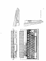
CASEWORK IDENTIFICATION ................................................. .
3
PCB LAYOUT ...................................................................................................... .
4
PCB PARTS LIST ................................................................................................. .
5
PCB SCHEMATIC DIAGRAMS ............................................................................... .
7
KEYBOARD MATRIX ............................................................................................ .
7
I.C. PINOUTS FOR UNCOMMON CHIPS ................................................................. .
9
RF MODULATOR 251844 LAYOUT ....................................................................... .
11
251844 SCHEMATIC ...................................................................
11
RF MODULATOR 251311 LAYOUT .........................................................................
12
251311 SCHEMATIC ...................................................................
12
iii/iv
SERVICE MANUAL
MODEL PLUS 4 COMPUTER
Preliminary
OCT. 1984
PN-314001-04
Commodore Business Machines, Inc.
1200 Wilson Drive, West Chester, Pennsylvania 19380 U.S.A.
Commodore makes no expressed or implied warranties with regard to the information contained
herein. The information is made available solely on
an as is basis, and the entire risk as to quality and
accuracy is with the user. Commodore shall not be
liable for any consequential or incidental damages
in connection with the use of the information contained herein. The listing of any available replace-
ment part herein does not constitute in any case
a recommendation, warranty or guaranty as to
quality or suitability of such replacement part.
Reproduction or use without expressed permission,
of editorial or pictorial content, in any matter is
prohibited.
This manual contains copyrighted and proprietary information. No part
of this publication may be reproduced, stored in a retrieval system, or
transmitted in any form or by any means, electronic, mechanical,
photocopying, recording or otherwise, without the prior written permission of Commodore Electronics limited.
Copyright © 1984 by Commodore Electronics Limited.
An rights reserved.
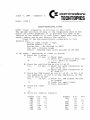
PLUS 4 PRODUCT SPECIFICATION
MEMORY
64K RAM. 60K RAM User accessible for BASIC programs.
ROM
32K ROM Standard iincludes operating system and BASIC interpreter) with 32K additional ROM con·
taining the built-in productivity software.
MICROPROCESSOR
7501 Microprocessor -
.89 or 1.76 MHz clock.
DISPLAY
40 Columns x 25 lines of text.
COLORS
128 Colors (16 calors; 8 luminance levels).
CHARACTERS
Upper & lower case letters, numerals and symbols. Reverse and flashing charachters. All PET graphic
characters.
DISPLAY MODES
Text characters. High resolution graphics. Split screen text/high resolution graphics. Muiticolor graphics.
RESOLUTION
320 x 200 Pixels
SOUND
2 Tone generators or 1 Tone and 1 white noise generator.
VOLUME
8 Volume levels
KEYBOARD
Full size typewriter style design
KEYS
67 Keys total. 4 Cursor control keys. 4 Programmed (reprogrammable) function keys (up to 8 user
defined functions possible). Col or control keys. HELP key. Upper and lower case character set. Graphics
character set.
INPUTS/OUTPUTS
PLUS/4 MODEM (User) port. Serial port. ROM cartridge and parallel disk drive port. 2 Joystick ports.
C1531 Cassette drive interface port. RF Output-channel 3 or 4. Video output-composite/
chrominance/luminance. Audio input/output. Power supply input.
1
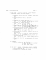
PLUS 4 PRODUCT SPECIFICATION (Continued)
FEATURES
Built-in extended BASIC 3.5 - over 75 commands. Built-in Machine Language monitor - over 12
commands. Built-in graphics and sound commands. Screen window capability. Reset button (Warm
start). Built-in integrated productivity software.
PERIPHERALS
C 1551 Fast Disk drive, C153 1 Datasette, MPS 802 Dot matrix printer, MPS 803 Dot matrix printer,
DPS 1101 Daisy wheel printer, C1802 color monitor.
OTHER PERIPHERALS
C1541 Disk drive, MPS 801 Dot matrix printer, C1702 color monitor.
PLUS 4 OVERVIEW
The Plus 4 system is based on the 7501 microprocessor, an HMOS version of the 6510. Video processing is achieved by the 7360 TED chip. 64K bytes of dynamic RAM are accomplished by 8 (64K
xl) LC: s. (See page l. The system program is contained in 2 (16K x 8) RaMs. The system supports
up to 1 28K x 8 of ROM banked in 16K sections. By software control, through the 7360, ROM can
be completely banked out and RAM banked in for a true 64K of RAM (minus 256 byte pages), allowing 60,671 bytes available for BASIC.
Keyboard and joystick scanning are accomplished by outputting the row data on the data bus while
addressing a particular register in the TED chip. This will in turn cause the TED chip to latch the column
information.
A standard serial port supports serial bus peripherals such as the 1541 disk drive and the various
serial printers. A cassette port is provided and the expansion port supports ROM cartrdiges. TTL serial
ASC!J is intended to drive an RS-232 adapter.
2
PARTS LIST
PLUSf4
TOP CASE ASSY
Top Case
Keyboard, 67 Key, KKR-l
Nameplate
Shield Clip, R
Shield Clip, F
C
C
C
C
C
251453-01
251501-01
251655-01
251855-01
251856-01
C
C
C
C
C
C
251454-01
950157-04
310156-01
310199-01
310197-01
310198-01
C
C
C
C
310196-01
310157
326189-02
904778-01
BOTTOM CASE ASSY
Bottom Case
Foot, Self-Adhesive
Paper Shield
Shield Chip
Shield Plate
Insulation Sheet
ACCESSORIES
Users Manual
Power Supply
RF Cable
Switch Box
c
~
Commodore Stock Part
'"
M
0
·2
•
,
0
•
,,•
~
•
••
0
••
0
"
,,
o
o
>
0
~
g
•
<•
m
u
•
••o
0:
,
I..
@'
®,
@'
@'
•
~
,
"
~
~
=
~
[
"0
•
~
." ®
o
"" I@'
;'"
~"I
""
I@'
I@'
I~,
,,"
""
c::::::ti!.C]
@,
,
10>
"
CW
o
.,
[
1
""
>
.,
,•
o
·•
·•
o
un
:~...
.. ..'" .,,",
0-
Issue 6, 1984
Computer 3
Model: PLUS 4
(:: TECHTOPICS
commodore
i" \980
CO~1MODOPc IlUS'~fS5
MADIIt<.f5
,~..:
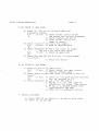
Troubleshooting Aides
NOTE: Visual inspection is critical in this unit!
The upright position of many of the components used on the
board can create problems. It is possible for them to be
shorted to the shield or to each other. Make sure they are
evenly spaced and do not contact the shield.
Areas of the peB particularly vulnerable to this
problem are:
Bottom right corner - caps
Bottom center - Jl-J6
Bottom left - Q3 shorted to FB57
Top left - ferrite beads
Center - Twisted caps (just outside of RF can)
1) NO VIDEO - Absolutely no video on screen
A) Check for 5 volts
O.K.
If not: 1) Check fuse
2) Check for twisted or bent caps
v
( 5 v. short to ground
3) Check Ll
B) Check for oscillation at pin 14 of Ul
O.K.
If not: 1) Check for good connection at
pin 14 of Ul
+
2) Ch ec k fo r good connect ion at
RI thru R7
Cl Check for LUM signal at pin 23 of 01, at pin 4 of
the modulator, at pin 8 of the modulator, at FB3
and at pinl of eN7
O.K.
If not: 1) Check for- LUM signal shorted
to ground
+
2) Check for open traces
3} Check modulator
D) Check for reset
O.K.
t
E) Check for control signals:
Signal
AEC
AEC
CAS
CSl
CSl
CSO
CSO
1. C.
Ul
U2
Ul
Ul
U20
Ul
U20
Pin
35
4
11
6
15
5
1
Signal
R/W
0
MUX
IRQ
RDY
BA
RAS
1. C.
Ul
Ul
Ul
Ul
U2
Ul
Ul
Pin
7
12
9
8
2
34
10
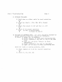
PLUS 4 Troubleshooting
page 2
2} BAD VIDEO - Scrolling lines on screen - Random
blocks on screen - Blurred display
A} Check JI-J6 for shorts to ground or each other
O.K.
t
B} Check reset for correct operation
O.K.
t
C) Check Ul for proper operation
O.K.
I f not; 1 ) Check socket for good solder
2) Check for bad Ul
t
D) Check U2 for proper operation
O.K.
I f not: 1) Check socket
2) Check for bad U2
t
E) Check RAM data lines for correct amplitude
O.K.
I f not: 1) Check for hot surface of RAM
2) Jump out RAM to verify
t
F) Check multiplexers U9, UI0 - signals at RP3
and RP4 should be similar in frequency and
amplitude
O.K.
I f not: 1 ) Suspect U9 or UI0
t
G) Check ROM for chip select signal at pin 22 of
U23 and U24
O.K.
If not: I} Check for signal generation
+
at U20
Hl Check that all ROM addresses are present and
correct amplitude
O.K.
If not: 1) Trace problem address AO-A15
t
I} Check U19, U23, U24 by replacement with known
good
3) NO POWER
A) Verify voltage +5
1)
2)
3)
4)
and +9 volts
Check for shorts to ground
Check switch
Check power supply
BAD BASIC - Random characters on screen - Random
colors - Power-up message is missing
A) Check Basic ROM U23
B) Check B thru I above (Bad Video)
PLUS 4 Troubleshooting
Page 3
5) NO CaLOR or BAD COLOR
A)
Check Ul
pin 14 for 14.31818 MHz with
frequency counter
O.K.
If not:
1) Check solder joints of CTl
and adjust for correct frequency
+
2) Check crystal, Ql and Q2
3) Check clock circuit for
opens or shorts
BI Check Ul pin 13 for Calor Out signal.
O.K.
If not:
1) Swap Ul w/known good
+
Cl Check modulator Ml pin 5 for Calor In signal
O.K.
+
and pin 6 for Calor Out signal
If not:
1) Check Ml operation
DI Check FB4 and CN7 pin G to see if calor signal
is present.
1) Check for shorts
6) NO SOUND or BAD SOUND
A) Check Ul pin 33 for SND signal
O.K.
If not:
1) Check socket for open circuit
...
2) Swap Ul w/known good
8) Check audio circuit for short to ground or loss of
signal.
O.K.
If not:
1) Check Q3 - Be sure emitter and base
are not shorted to 5 V.
+
Cl Check modulator Ml pin 2 for SND signal
1) Adjust LF. can (top right of
modulator) for clean, loud volume
2) Ml pin 2 to ground should read
approximately 480 ohms
3) Check Ml for component failure
7) SERIAL FAILURES
Al Check FB23-26 for shorts to shield or each other
8) Check U7, U2 and CN2
PLUS 4 Troubleshooting
8)
page 4
KEYBOARD FAILURES
A) Check pins on ribbon cable for good connection
O.K.
t
B} Check for shorts - CN5, CN6, FE's, Diodes
O.K.
t
C) Check chip select to U27 and the I.C. U27
O.K.
t
D) Check Ul for proper operation
O. K.
If not: 1) Check socket
2) Check for bad Ul
t
9) FAILURES IN SOFTWARE MODE - All units should be checked for
proper operation, when any repairs are necessary.
To Check: 1) Press 'FI' on keyboard
2) Press 'Return' to enter Word processing mode
3) Press 'Commodore' key and 'c' key at the same
time
4) Type 'tc' and press 'Return' to enter
Spreadsheet
5) Press 'Commodore' key and 'c' key again
6) Type 'tw' to return to Word Processing mode
Watch for video or loading problems, then:
A)
Check jumpers at JI-J6 for correct connection
O.K.
t
B) Check Ul, U2, U25, U26
PARTS LIST PLEASE NOTE:
PLUS/4 peB ASSEMBLY #310163-01
Commodore part numbers are provided for reference only and do not indicate the
availability of parts from Commodore. Industry standard parts (Resistors, Capacitors,
Connectors) should be secured locaJly. Approved cross-references for TTL chips,
Transistors, etc. will be available in manual form through the Service Department
in November of 1984. Unique Of non-standard parts will be stocked by Commodore
and are indicated on the parts list by a "C".
INTEGRATED CIRCUITS
Ul
U2
U3
U4
U5
U6
U7
U8
U9-10
U11-18
U19
U20
U21
U22
U23
U24
U25
U26
U27
DIODES (Continued)
Icont.)
7501 Custom Microprocessor
CR1l-20
C 251536-01
6551 A (Synertek)
901895-02
74LS08
901521-03
65298 Single Port Interface
C 251640-03
74LS04
901521-02
7406
901522-06
901523-01
555
74LS257
901521-57
4164-2D-RAM
901505-01
7700-010 PlA
C 251641-02
74LS139
901521-18
74LS175
901521-34
74lS27
901521-22
23128 ROM TED Basic
C 31800B-Ol
23128 ROM TED Kernal
C 318005-04
23128 FUNCTION ROM, 3+ 1 LOW
C 317053-01
23128 FUNCTION ROM, 3+HIGH
C 317054-01
B5298 Single Port Interface
C 251640-03
TRANSISTORS
01-03
04
2SC 1815
2SD 880
Tip 29A
2SD 1266
?V,:
S~
902693-01
902694-01 Sub:
902653-01 Sub:
902694-04
Rl
R2
R3
R4
R5
R6
R7
R8
R9
Rl0
Rll
R12
R13
Rectifiers DBA20C
251026-03
Zener RD 6.B EB 900927-01
IN 914 Sub:
900850-16
IN 4148 Taping
251819-21 Sub:
Diode, IN 4148
900850-01
AU values are in ohms-1/4 W
5% unless noted otherwise.
RESISTORS -
R14
R15
R16
R17
R18
R19
R20
R21
R22
R23
R24
R25
4.7K
10K
470K
220K
18K
1.5K
470K
lOOK
lK
lK
12K
10K
lK
240
250
lOOK
1.5K
47K
lOOK
3K
lK
lK
lK
lK
lK
RESISTOR PACK
RP1, 2
RP3, 4
3.3K, 6 PIN
B8, 8 PIN 4 ISOLATED
Cl
C2
C3
C4
Elect
Ceramic
Film
Film
Ceramic
Elect
Elect
Ceramic
Trimmer
Ceramic
C5-C6
Bridge Rectifiers S2VB10 5indengen
215026-01 Sub:
Bridge Recitifers DBA20B Sanyo
251026-02 Sub:
TI,'OT=~
CR2
Bridge
Sanyo
Diode,
Diode,
Diode,
902441-29
326149-06
CAPACITORS
DIODES
CRl
CRl
7360 VLSI, Text Dislay (TED)
Sub:
C 251535-01
8360
C 251535-02
I BEVF:VF: tJ24 SHOULD
Pl:~?_D
C7
C8
C9
ClO
Cll
C 318004
0.1
0.1
/IF 25V
/IF 25V
0.22 }IF 100V
0.22 }IF 100V
0.22 /IF 50V
2200 /IF 16V
1O}lF 16V
0.1 /IF 25V
40 pF
22 pF 50V
900100-40
251075-06
900150-11
9OO15Q--ll
900022-01
900101-33
900100-25
251075-06
251029-02
251070-14
r~
5
PARTS LIST - PLUS/4
PCB ASSEMBLY #310163-01 (Continued)
MISCELLANEOUS (Continued)
CAPACITORS (Continued)
C12
C13
Cl.
C15-C16
C17-C18
C19
C20
C21
C22
C23
C24-C26
C27
C28-C29
C30
C31-C32
C33-C40
C41-C51
ClOD
Ceramic 220 pF 50V
251071-26 Sub:
Ceramic 220 pF 50V
Ceramic 150 pF 50V
Sub:
Ceramic 150 pF 50V
Ceramic 0.1 ~F 25V
Ceramic 0.1 ~F 25V
Ceramic
10~F 16V
Ceramic 0.01 ~F 25V
Elect
10 ~F 16V
Ceramic 0.1 ~F 25V
Elect
10 ~F 16V
Elect
1 ~F 16V
Ceramic 0.1 jiF 25V
10j1F 16V
Elect
Ceramic 0.1 J.lF 25V
Elect
10J.lF 16V
Ceramic 0.1 j1F 25V
Ceramic 0.22 J.lF 25V
Sub:
Ceramic 0.22 /LF 50V
Ceramic 0.1 /IF 50V
Sub:
Ceramic 0.1 /LF 50V
Ceramic 0.1 Jl.F 50V
Sub:
900463-08
251071-24
900462-41
251075-01
251075-06
900100-25
251075-01
900100-25
251075-06
900100-25
900100-16
251075-06
900100-25
251075-06
900100-25
251075-06
251075-07
900022-01
900020-06
FB2-14
FB15-21
FB22-26,
FB28-38,
FB40
FB41-58
FB59
FB60
FB61-63
FB64-65
EM1,2
EMI Filter
CNl
Connector 4 PIN (power supply)
C 251614-01
Connector 6 PIN DIN (serial bus)
C 903361-01
Connector 7 PIN MINI DIN (cassette)
C 251616-01
Connector 50 PIN Female Edge
(exoab)
C 251630-01
Connector 8 PIN MINI DIN
(joy 1 & 2)
C 251259-01
Connector 8 PIN DIN (audio/video)
325573-01
Connector 18 PIN (keyboard)
C 251841-01
CN2
CN3
CN.
CN5-6
CN7
9000010-01
900010-20
CN8
Ferrite bead
Ferrite bead
325563-01
903025-01
Ferrite bead
325563-01
Ferrite
Ferrite
Ferrite
Ferrite
Ferrite
903025-01
325563-01
903025-01
325563-01
903025-01
bead
bead
bead
bead
bead
251842-01
MISCELLANEOUS
Yl
Y2
SWl
SW2
Ml
Crystal 14.31818 MHZ 251081-01
Sub:
Crystal 14.31818 MHZ 251081-02
CryStal 1.8432 MHZ
900555-02
Switch, Rocker
(PC Mount)
Switch, Push Button
C 251587-01
RF Modulator
Sub:
RF Modulator
C 251844-01
C 251260-01
251311-01
C -
L1
L2
L3,L3
Fl
Noise Filter
Line Filter
Sub:
Sub:
Coil Inductor 1.2 uHpt
Sub:
251264-01
906127-01
251701-01
Fuse 250V 1.5A
Fuse Clip
Cartridge Guide
Shield Box
Shield Cap
903556-18
906102-01
310171-01
C 310172-01
C 310173-01
901152-01
325570-01
Commodore Stock Part
6
1.
17
RE.
13
8
6
2
16
9
RUN
5
CD
1
CLR
CTRl
STOP
SPACE
C.
Q
2
3
W
A
SHIFT
Z
S
E
•
5
R
D
X
C
F
T
6
7
Y
G
V
8
H
U
8
9
I
J
N
M
K
0
0
(i)
{I
P
L
@
<-
•
.
11
10
@
DEL
18
~
RETURN ~
;
,
/
Ese
-
+
'"
@
f1
12
13
HELP
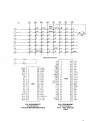
KEYBOARD MATRIX
A2
Al
M
VOO
~OIN
Roy
IRO
AEC
VCC
A
Al
A2
A3
fi
1
2
3
4
5
6
7
8
9
A4
10
A5
A6
A7
AB
A9
Al
All
A12
A13
GNo
11
12
13
14
15
16
17
18
19
20
7501
40
RES
39
R/W
38
O~
37
01
36
02
35
03
34
04
33
05
32
06
31
07
30 -,·P0
29
Pl
28
P2
27
P3
26 -P4
25
P5
24
P6
23
GATE IN
22 -A15
21 -A14
PIN ASSIGNMENT
U2-251536-01
CUSTOM MICROPROCESSOR
CS~
CSl
R/W
IRQ
MUX
RAS
CAS
<1>0
COlOR
elK
IN
K~
Kl
1
2
3
4
5
6
7
8
9
10
11
12
13
14
15
16
17
18
19
20
21
K2
K3
K4
K5
K6
K7 - 22
SYNC
vSS
23
24
7360
48
47
46
45
44
43
42
41
40
39
38
37
36
35
34
33
32
31
30
29
28
27
26
25
-A3
-A4
-A5
-A6
-A7
-A8
-A9
-Ala
-A 11
-Al2
-A13
-A14
-A15
-AEC
-BA
-SNo
-07
-06
-05
-04
-03
-02
-01
-o@
PIN ASSIGNMENT
U1-251535-01
VLSI, TEXT DISPLAY
(TEDI
SHIFT LOCK
SW
-
,
~
~
'r.
-
~~
~:
~.
I~
~~
.
--
0
>
>
~" --"j.
,. g ~
~ ~ 8~
G:s ~ ~
c.,~
->
'fl'.1.1 .~-("
" ~ ~
,I ~~ ~
~
~~Pf
~
~
I
'"
2
,
u
'"
I"
.
~:~
• " ,
'~ :7 ~ ',> ~
• " ,
'il'
I
I ". •
la~s
0
,"
<
S3
J ~J
~ ~I
.
~
~~
~
;]
~
.
.
.•
~
~, ~~
0:
~
~
,I
,
<
I,
' I"I,
v
u
v
<
••
~
lee
;
~
;,
.
~:
~"
IV Il
'"
Il
•,
".
. 01'"'
>
•
J
",
~"
,.
~
-::~c
-,.
'"
F"
~
ID
~Cl
u
I
)"11'
~ ,~
~!~
~HI~ ~
'"
,
C?,
<
&~
~l
c~
;;:'" of
,
-."
I~
o 2YI' 8
>1
1::
'"
"
,I;;
I·
"
~
' ..
"
.<!
~l:!
,~ ~
~
10
I: I.
"
~
,
§I l§1 ~I gl
J
<>:
15! 1
~f,"
: 02 : ~
~ ~
« .. « ..
~
~
~[
"
- '::! ,...
~
N
~
0
V
<
~
~;
•I•
~
l
~
:~
:;t
~
::
-..
;
~, ;; ~ rf
i'1'j1
" ~~
~
.
,! .... §( ~'J;;
I
~" !-~1--.
'7'1 ~ ~
}'S=('I ~k'J ~ <
0
e
'''-" ~
::: j:£
~}-11'
,
....
"'
~I,!
<.
3
~~
u.
:
~ I~
>
=
~
;iI~
III ..::;,:
,iC:!1> :fi
~
0
8
,
-~
w
~
~I~
.
-11'
El,
0
~,
0
~:;'~
,~
<
&
"
91"
8=
~
.0 -';
:
<
Il
..
~.
~
,
•. ~
t~~
-
,
'---
1:<>-1"
~"l
," ... -
~
1
.
,... ~ zZ
~a. SO
•
~
_:
~I!
3"
u
M1 SCHEMATIC ON PAGE 11
TRANSMIT/RECIEVE CHARACTERISTICS
PIN
CONFIGURA TlON
VSS CS0 CS1 RES RXC XTL 1 XTL0 RTS CTS TXO OTR RXO RS0 RS1 -
1
2
3
4
5
6
7
8
9
10
11
12
13
14
6551
28
27
26
25
24
23
22
21
20
19
18
17
16
15
CHARACTERTISTICS
-02
2 MHZ
SYM
MAX
MIN
-R/W
-02
-IRQ
-07
-06
-05
-04
-03
-02
-01
TRANSMIT/RECEIVE
CLOCK RATE
TRANSMIT/RECEIVE
CLOCK HIGH TIME
TRANSMIT/RECEIVE
CLOCK LOW TIME
XTL1 TO TXD
PROPAGATION DELAY
RTS PROPAGATION
DELAY
IRQ PROPAGATION
DELA Y ICLEAR)
-00
-OSR
-OCO
UNIT
•
tCCY
400
-
ns
tCH
175
-
ns
tCL
175
-
ns
tDD
-
500
ns
tDLY
-
500
ns
tlRQ
-
500
ns
-VCC
Itr, tf
~
10 to 30 nsl
* The Baud Rate with External Clocking is:
BAUD RATE
U3-901895-02
ACIA
_--,1_ _
16 x T CCY
1SYNERTEK 1SYP6551 A 12 MHZ
PIN
CONFIGURATION
PIN
CONFIGURATION
FE 17 16 15 14 13 12 11 10 F7 F6 F5 F4 GNO -
1
2
3
4
5
6
7
8
9
10
11
12
13
14
28
27
26
25
24
23
CS
R/W
00-07
L
L
DATA BUS
TO PORT
-110
-111
L
H
PORT TO
DATA BUS
-112
H
-VCC
-18
-19
X
ISOLATION
22 -113
21
20
19
18
17
16
15
U19-251641-02
PLA
-114
-1115
-CE
-F0
-Fl
-F2
-F3
L
H
X
~
~
~
LOW LEVEL
HIGH LEVEL
IRREVELANT
MOS
R/W P0 -
Pl
-
P2 P3 P4 P5 P6 P7 VSS -
6529B
U5/U27-251640-03
SINGLE PORT
INTERFACE
1
2
3
4
5
6
7
8
6529
9
10
3 MHz
20
19
18
17
16
15
14
13
12
11
-VOO
-CS
-DB0
-OBl
-082
-OB3
-OB4
-OB5
-OB6
-OB7
"l,l
.".11
"
I.~~~
lll'-4
(OlOR
'NO
1
c::;.
=
r
I~!f
•.ov
r-
I
.sv
"'1 I
1<1]
III
t
7
LUM IN
(OWR IN
cUt..! OUT
r
4.
I
COMn", 1
11
J7
"A2
LLJ' .
,.,
3
COlOR OUl "
CND
l
~
M
"A.
COlOR
A1
N~T[
A8
1«.,..
Irl~1
111~
2.q~.fL
+~
~2r
J '''''Pi'
>l15
24Q.n.
1
"
"
ICb'!'\
"'"
h:
~.
"
11.31e18 f,lHl '-J15C
~.l,',~f'cM:'
r
D
Cl
~
CH
•.,\I'p[
I".P'
"4.7K
'qAl
_
*"
733P[
c,'
1.2,...11
r-.,
Ql
!":'o
D4
[ D,
""
Dl
Q'
25C18'5
7
.L.
~
....
2 in
>
"
~; I~
22Ql.n-
4
C51 SENSE
~
eST MTR
• 9V
I
0--.,.----,
~5V
REG
0ll:lQ1
liT 1.1,t.,MP
c",
1
2
1\
FBI3
---
T
0-10
I
Fll1E~
-
I
, j
[.>.1,1.
J
. 1#f-
POWER
--.
I
"
1
LINE FlL lER
a.
"
CB •
.,,./
3
3Il . ij''''>1
u
A
_I.'V
1
I
'.L1
17
c=>
fBI5
RAse:
~o
c'
FBI"
c::
~.«,..T
-
+
J
"
i9
18
17
'"
il.
"
Z
,
§
~
m
is
"
-+
WU
I ''''''AI
C
D
c
HIGH
e
~
C2 1..0"'"
c..:;,-
1
C2,"IGIoI
L:>-
8
,
c:::>-
~=
==
c::>
=
",n
--.T
,.
13
BA
~
,
+5Y
2
(°'"'"1" ,,
12
IW
cc
"
•
fBS!!o
"~"
Ne
c::::>------C:J-
T.IC~ f
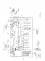
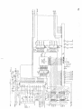
Plus 4 Schematic #310164 (2 of 41
~B
""
~
n
z
" •
"
"
I.1UX
AEC
~
r
•5 z"z
"'"
R!W =c:::>c::>
-::-
~~~EG
I
~,~ ~~--!---!_O
~
l±J~'J
',~
~
rrrnL~'-~I;;-t-'--T-1
1 \' -••
-
SAE5E"T
'hAC
A55Y
K
9
L
? PIN DIN
q"C
I'tl.C!MC
I~
Z
25D8811J
w.~~~
I ."y
J
I
o.'jy
c:::>-
~ I~
r-~-----"1
11
Cl LOW
CSI
,BII
e51 RD
(ST WRT
c
c
N
1.3
'.. 5K
,.
p
R
P
'.
_D2_ _
-sv
l5Q f
T
QP-
!!J.
(lK IN
U
,
"
1. CI<..L . ,1,-(
,e
--Y "
25(1815
L
(15
t-------c=>
~:~I~f!
1
J1 .1,..1
"
41~.f\.
W
V
CAiS
'13
'I,
,sv
47<2.IL
,
"l
RI(/,
_ 11)4 K.f\.
I, I
"".
'"
'"
C2~
Q3
l'~
1211
'"
4
5
I
-L
25CI815
-.
'~~f
MI
SEE
Iq~
---,
RF DUT--...J
'B
RI2
t
1~~K _
ec
MODULAlUR
j
t: SND
~:'"
1<9
11(
I
7
~'5'J o-------flII
BB
Z~
PINOUTS ON PAGE 8
·11
COMMODORE
RATION
VENDOR
PART
APPROVED
SOURCE
PART
1
CYCLES
POWER
Ins)
ACTIVE
(MWI
STANDBY
IMAXIIMWI
NUMBER
OF SUPPlY
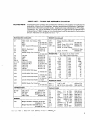
901505·01
HITACHI
HM4864-3
200
335
330
20
901505-01
NEe
pPD4164-2
200
375
250
28
901505-01
MITSUBISHI
M5K416NS-20
200
330
275
28
901505-01
MOSTEK
MK4564N-20
200
345
300
22
901505-01
OKI
MSM3764-20
200
330
248
23
18
....IIC RAM
901505-01
MICRON
TECHNOLOGY
MT4264-3
200
385
300
30
5-01
901505-01
HITACHI
HM4864P-3
200
335
330
20
901505-01
MATSUSHITA
(PANASONIC)
MN4164P-20
200
330
275
27.5
901505-01
SIEMENS
HYB4164-3
200
330
150
20
901505-01
SHARP
LH2164-Z1
200
330
248
28
901505·01
HITACHI
HM4864AP-3
200
330
242
20
901505-01
TOSHIBA
TMM4164AP-20
ZOO
330
275
22
16
15
14
13
12
11
10
9
~VSS
~CAS
~DOUT
~A6
~A3
~A4
~A5
~A7
~I~
l
.TOR
-
OCK
\TOR __
-
.
1£
:z:
(J)
I
i
~
CC
(J)
ARRAY
w
CC
u.
w
CC
w
(J)
I~
1
L
w
0
w ...i
(J)
0
(J)
::J
::J
Cl U
Cl
(J)
~
MEMORY
ARRAY
Z
w
DEC.
g
w
0
...i
0
(J)
w
ROW DEC.
---
(J)
(J)
.
(J)
le
MEMORY <l:
:z:
ARRAY (J)
w
L--.
OATAIN
BUFFER
DATA OUT
BUFFER
-0
DIN
f-o DOUT
~
VCC
CC
u.
w
CC
~ MEMORY w
ARRAY (J)
Z
w
U
<:: r--~ ~ ROW DEC
---'"" VSS
-1VBB GENERA
(J)
u
(J)
(J)
0
~ :::; ROW
f::: r--u
(J)
::J
a:
...i
0
u
ROW DEC.
<l: MEMORY
(J)
w
t
MEMORY
ARRAY
0
le
w
u.
u.
III
t
w
MEMORY
ARRAY
-
-
, •
u
OCK
.TOR f---
I
R/W SWITCH:
t
-
-
NUMBER
ACCESS
TIME
(nsl
MEMORY
ARRAY
w
0
...i
0
MEMORY
ARRAY
u
i
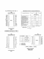
FUNCTIONAL DIAGRAM
QA
PI
,
I
w
0
• , " "
It-
.
!1
rH!'
,b
~f
~
24 PIN
MALE £0(,£
.
• =
I
~~
~''7
.
I~ i7
•
1-,.
~"
iJ
(H"~
~
1
z~
Q<
".
a~
~ =
!
.
J
ri'I_
01
~~
;Iit
D.
~~
".
~Ih
05
~&~th
D'
~~
~,
~~
§If.;~
9F-----
E
~
,
,
«
,~
~<
0
~
E
"
d.
,,.
"
0D
J
Q
Q-
I~
;F.-!
"
I~
0
Q
~
Q
I~
~~
2
:;
0
"-
0
~
"
~
.•"
PIN
CONFIGURATION
NC -
A12 A7 A6 A5 A4 A3 A2 Al ArJJ 01 02 03 GNO -
1
28 -VCC
2
27 -CS,
3
26 -A13
4
25 -A8
24 -A9
5
6
23 -A 11
7 23128 22 -CS,
8
21 -AlrJJ
20 -CS,
9
10
19 -08
11
18 -07
12
17 -06
13
16 -05
14
15 -04
U23-318006-01
ROM - BASIC
PIN
CONFIGURA TlON
NC -
A12 A7 A6 A5 A4 A3 A2 Al ArJJ 01 02 03 GNO -
1
28 -vcc
2
27 -CS,
3
26 -A13
4
25 -A8
5
24 -A9
6
23 -A 11
7 23128 22 -CS,
8
21 -AlrJJ
9
20 -CS,
1 rJJ
19 -08
11
18 -07
12
17 -06
13
16 -05
14
15 -04
U24-318005-04
ROM - KERNAL
,,-
(!l
o
0
!i:~
~
J-''a
~
~~i
15
~
;
..H~,
o;q ....
o;:;,~~
.§
-
-I
l
~~~~
"
n .. }
HI.
J <5 0 13
•
.: .. Oi
" ~~ JI ~
~1
,"'-
f-11-~'---------"
~ ~~
1~, I - r- ~~)~IJM'·lJfRlJ*.JJJffim'~mm-''W--ffio"- I I'
-
J
bJ
~- - l' }-
2
L"
-
-
-
I-
-"
-
1" }-
(! I •
0r-~r--I"
I
rf-1 " I "
o
,
.
"
I~;;
I
.
f""
, I
J~ - - - -: --; - _, - - - .!- ___ _
;
"
-
J
I-
LI
( I
QI
22r JJof'
---
COLOR. IN
.
""".. ~7!;
~"
~
'<-
"''".,.,
LUH IN
DI
Gj
"'L
s.
~4
"-
Th
1
us 2>0{'
C4
U
~;A ~~
CJ
pT
.jjOP
eOLOR oUT
~~
~ C('lj
.,~
~-
-""
/.20
cS
(SOP
.,..
3VP
>-{)
,,~
Lun
OUT
(OHP OuT
~.
':).
,,"l.
",'1.
1?l8 ~,"'J<:-/(J*
1;60
TB
crop
;;..7k
~14
('8
S60 47o:::nP l4
H)L~ ,,<;;
§'"
C6
Clit
RIS
RlJ
~~
c9
22P
,it
J3P
c;;- 8~
~Q3
SP
""
"l!~
",;
"
11;,';
AUDIO IN
""
C21
/0.«
C20
.220>1
..,s
6.8k.
04
;
:
"
m
J.jl<-4.2~
LS
~(!J
2Jf'
.l2P ;;.
8
1<23
.2.2k
~:~
':~
t
vl(-/
u:[
$$1
~
Dj
p
en
/SI'
~,:-
<),.
"<
"~"
N
C,.
3J?
TOP VIEW
~
L7
..
~
"
"
~I
J?F OUT
...~
""
04
sf-/,
.;;- C22
.....
,2(, ~
~.81C
"DP
COMPONENT PART8 VALUE: R = n, C
Q3. Q4: 28C460 OR EQUIVALENT.
Q1. Q2: 28C1684 OR EQUIVALENT.
03.04: 188198 OR EQUIVALENT.
02
: 188110 OR EQUIVALENT.
01
: 188119 OR EQUIVALENT.
e2j
<rJ'
/
PHONO JACK/
'""
I
e/8
09?
NO.
RC~
0
L6
~ ~
1<2/
68 -/$0
C/9
;.2OP
CH~
D£ TAIL (CH. SN)
= F.
L
TERMINALS
1
N.C.
2
AUDIO SIG. INPUT
3
+B 1+5V)
4
SYNC + lUM. SIG. INPUT
5
COlOR SIG. INPUT
6
COlOR SIG. OUTPUT
7
COMPO. SIG. OUTPUT
8
SYNC + lUM. SIG. OUTPUT
9
RF OUTPUT
10
H
CHANNEL SELECT SW.
REAR VIEW
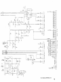
RF Modulator Lavout and Schematic #251844
11
II Cl
--- .>:sOP
..
Q~
221'
COlOfil. ,N
.,
.."
-~
Lilt? IN
....
"'<;
~~
'<"
~
/)1
~
'"'"
.... "4
So
.,!\
~
C2S :;.20{'
!Z,
~/~~
c"
J~OP
COLOR OUT
~l
('4
...
"..
'20
CS
UP
,,~
-<If
~20P
~
~
,~
LUN
oUT
CONP OUT
"'a
", ~~
';!~
",
Rfa ""."!JI!:_/Q,t
"'J
S..,
;-B
IV4 C'8
....c9
$"60 47<XXJP L 4
1~ ~~
"
H~
CoS
"tI:Op
L
I?2J
2.:U.
A.UDIO IN
CLo
22001'
5~
C2,
FOP
=
'""
CtlJik
"~S
22P
:J..7k
cro
Sf
.."'"..
,j3P
-" Q3
CI(,....
~
,"- UP ('-..
ii<
Dj
:~
Lt
~
t
f'J ,t~ ~
""-/
'$;f
P
en
ISP
"-if'.L6
M
Cl'
e/8
.llP
J1p
:
I~t
~ <22
....
m
J.Jj(-l.2~
..,•,
~
~
::•
I?F OUT
I
."
~
"
J'6~
04
"KIJ,
COMPONENT PARTS VALUE: R ~ O. C
Q3. Q4: 2SC460 OR EQUIVALENT.
Ql. Q2: 2SC1684 OR EQUIVALENT.
03.04: lSS198 OR EQUIVALENT.
02
: lSSl10 OR EQUIVALENT.
01
: lSSl19 OR EQUIVALENT.
1t21. ...---. CLj
("'"
/
TOP VIEW
R2/
~6-ISO
8
6.11< 1.3 I(
JACI'V
J.? ,
~~
<.;
221'
NO.
ReA . .GHONO
C,9
/,20P
CH 4.
-iff+
-----t--
(H.3
DLTAIL (CH.SN)
~
F. L
TERMINALS
,
N.C.
2
AUDIO SIG. INPUT
3
+61+5VI
4
SYNC + WM. SIG. INPUT
5
COLOR SIG. INPUT
6
COLOR SIG. OUTPUT
7
COMPO. SIG. OUTPUT
8
SYNC + LUM. SIG. OUTPUT
9
RF OUTPUT
10
H
CHANNEL SELECT SW.
REAR VIEW
RF Modulator Layout and Schematic #251311
12
Issue 7, 1984
Model: C16, PLUS 4
Computer 4
(:: TECHTOPICS
commodore
LINE DEFINITIONS
AO to AlS
AEC
ATN
BA
BRESET
Cl HIGH, Cl LOW
C2 HIGH, C2 LOW
CAS
CLK IN
COLOR
COMP
CE
CS
CSO
CSl
CST MTR
CST RD
CST SENSE
CST WRT
CTS
DBO to DB7
DCD
DRAM
DRAM ADD
DSR
DTR
EXT AUDIO
GATE IN
IRQ
KO to K7
KERN
LUM
MUX
PO to P7
RAS
RESET
RxC
RxD
R/W
RTS
SND
TED
TxD
f 0
f2
Address Bit 0 to 15
Address Enable Control
Attention
Bus Available
Buffered System Reset
External Cartridge Chip Select
"
Dynamic RAM Column Address Strobe
Master Clock (Single Phase, 14.31818 MHz)
Chroma Output
Composite Chroma and Luma
Chip Enable
Chip Select
Low ROM Chip Select
High ROM Chip Select
Cassette Motor Control
Cassette Read
Cassette Sensor
Cassette Write
Clear To Send
Data Bit 0 to 7
Data Carrier Detect
Dynamic RAM
Dynamic RAM Address
Data Set Ready
Data Terminal Ready
External Audio Input
R/W GATE
Interupt Request
Keyboard Latch 0 to 7
Kernal ROM Control Line
Composite Sync and Luminence
Address Multiplex Control
Port Bit 0 to 7
Dynamic RAM Row Address Strobe
System Reset
Receive Clock
Receive Data
Read/Write Line
Request To Send
Sound Line
Text Display
Transmit Data
System Clock (Varies between 1 and 2 MHz)
Artificiall2, Address Valid Rising Edge,
Data Valid Falling Edge