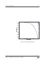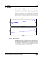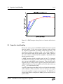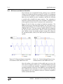
1
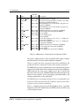
Operation and Service Manual
300 MHz Dual Inverting Driver Amplifier
SIM954
Stanford Research Systems
Revision 1.2 • April 8, 2015
Certification
Stanford Research Systems certifies that this product met its published specifications at the time
of shipment.
Warranty
This Stanford Research Systems product is warranted against defects in materials and workmanship for a period of one (1) year from the date of shipment.
Service
For warranty service or repair, this product must be returned to a Stanford Research Systems
authorized service facility. Contact Stanford Research Systems or an authorized representative
before returning this product for repair.
Information in this document is subject to change without notice.
c Stanford Research Systems, Inc., 2008 – 2015. All rights reserved.
Copyright Stanford Research Systems, Inc.
1290–D Reamwood Avenue
Sunnyvale, CA 94089 USA
Phone: (408) 744-9040 • Fax: (408) 744-9049
www.thinkSRS.com • e-mail: [email protected]
Printed in U.S.A.
Document number 9-01649-903
SIM954
300 MHz Dual Inverting Driver Amplifier
Contents
General Information
Safety and Preparation for Use . . . . . . . . . . . . . . . .
Notation . . . . . . . . . . . . . . . . . . . . . . . . . . . . .
Specifications . . . . . . . . . . . . . . . . . . . . . . . . . .
1
2
Operation
1.1 Quick Start . . . . . . . . . . . . . . . . . . .
1.2 Operation Inside the SIM900 Mainframe . .
1.3 Operation Using an External Power Supply
1.4 Interfaces . . . . . . . . . . . . . . . . . . . .
General properties
2.1 DC Characteristics . . . . . . . . . . . . . .
2.2 AC Characteristics . . . . . . . . . . . . . .
2.3 Noise . . . . . . . . . . . . . . . . . . . . . .
2.4 Crosstalk . . . . . . . . . . . . . . . . . . . .
2.5 Isolation . . . . . . . . . . . . . . . . . . . .
2.6 Power Supply and Thermal Considerations
.
.
.
.
.
.
.
.
.
.
.
.
.
.
.
.
.
.
.
.
.
.
.
.
.
.
.
.
.
.
.
.
.
.
.
.
.
.
.
.
iii
iii
iii
iv
.
.
.
.
1–1
. 1–2
. 1–2
. 1–3
. 1–4
.
.
.
.
.
.
2–1
. 2–2
. 2–4
. 2–8
. 2–9
. 2 – 10
. 2 – 12
3
Application notes
3.1 Resistive Loads . . . . . . . . . . . . .
3.2 Capacitive Load Handling . . . . . . .
3.3 Inductive Loads . . . . . . . . . . . . .
3.4 Transformers . . . . . . . . . . . . . . .
3.5 Load Impedance Matching Examples
3.6 Bridge Configuration . . . . . . . . . .
3.7 Typical Application: a High Voltage
Noise, DC-DC Converter . . . . . . . .
3.8 Common Mode EMI/EMF . . . . . . .
3.9 Overdrive Behavior . . . . . . . . . . .
3.10 Miscellaneous Loads . . . . . . . . . .
3–1
. . . . . . . . . 3–2
. . . . . . . . . 3–3
. . . . . . . . . 3–5
. . . . . . . . . 3–8
. . . . . . . . . 3 – 10
. . . . . . . . . 3 – 11
Isolated, Low
. . . . . . . . . 3 – 12
. . . . . . . . . 3 – 16
. . . . . . . . . 3 – 18
. . . . . . . . . 3 – 20
4
Calibration
4–1
4.1 Getting Ready . . . . . . . . . . . . . . . . . . . . . . . 4 – 1
4.2 Offset Voltage and Input Bias Current . . . . . . . . . 4 – 1
i
ii
Contents
5
Circuitry
5.1 Circuit Description . . . . . . . . . . . . . . . . . . .
5.2 Parts Lists . . . . . . . . . . . . . . . . . . . . . . . .
5.3 Schematic Diagrams . . . . . . . . . . . . . . . . . .
SIM954
5–1
. 5–2
. 5–4
. 5–7
300 MHz Dual Inverting Driver Amplifier
General Information
The SIM954 300 MHz Amplifier, part of Stanford Research Systems’
Small Instrumentation Modules family, is a dual, inverting, precision
wideband amplifier with up to ±10 V output voltage and 1 A output
current.
The module can be used to drive many types of light laboratory loads
which exceed the capacity of typical instrument outputs without
imposing the limitations and cost of typical high power RF amplifiers.
Safety and Preparation for Use
The front-panel BNCs are all grounded to Earth ground, the powerline-outlet ground, and the metal chassis of the module. No dangerous voltages are generated by the SIM954. However, if a dangerous
voltage is externally applied to the module, it may be present on all
BNC connectors, the chassis, the SIM interface connector, and may
cause injury or death.
The SIM954 is a single-wide module designed to be used inside the
SIM900 Mainframe. Do not turn on the power until the module is
completely inserted into the mainframe and locked in place.
iii
iv
General Information
Specifications
Performance Characteristics
Property
Gain
-3dB Bandwidth
Gain Flatness
Min
Typ
−4 (12dB)
300 MHz
1 dB
−60 dB
−40 dB
Crosstalk
VSWR
Isolation
Slew Rate
4000 V/µs
Output Amplitude
10 V
Peak Output Current
1A
Average Output Current 500 mA
Output Impedance
Input Impedance
Input Offset Voltage
Input Bias Current
Operating Temperature
0
Power Supply Voltages
Supply Current
Max
1.2 : 1
1.6 : 1
−70dB
−40dB
Remarks
3% max. gain error
small signal
DC to gain peak
at 1 MHz
full BW
DC to 100 MHz
DC to 300 MHz
Output to input DC to 1MHz
Output to input DC to 300MHz
into 50 Ω
into ≤ 7 Ω
one channel or sum of both channels
3.3 Ω
50 Ω
1 mV
10 µA
40◦ C
user trimmable
user trimmable
±1 A
Internally current limited
−15 V,+15 V
Table 1: SIM954 Specifications
SIM954
300 MHz Dual Inverting Driver Amplifier
1
Operation
Following is a short overview on general guidelines for the operation
of the SIM954.
In This Chapter
1.1
1.2
1.3
1.4
Quick Start . . . . . . . . . . . . . . . . . . .
Operation Inside the SIM900 Mainframe . .
Operation Using an External Power Supply
Interfaces . . . . . . . . . . . . . . . . . . . .
1.4.1 SIM Interface Connector . . . . . . . .
1.4.2 Direct Interfacing . . . . . . . . . . . .
.
.
.
.
.
.
.
.
.
.
.
.
.
.
.
.
.
.
.
.
.
.
.
.
.
.
.
.
.
.
1–2
1–2
1–3
1–4
1–4
1–4
1–1
1–2
1.1
Operation
Quick Start
The SIM954 contains two mostly independent, identical small RF
power amplifiers with a gain of −4 (12dB) into 50Ω and a −3dB
bandwidth of 300MHz. The output voltage limit of ±10V can be
achieved with a modest ±2.5V input voltage, so most test equipment
can drive a SIM954 channel to its voltage and power limits.
The module was specifically designed to drive laboratory loads like
magnetic coils, capacitors, piezoelectric and electrochemical cells,
small motors, heaters etc.. While these loads often require currents
and voltages beyond the range of many test instruments, driving
them with expensive and bulky power amplifiers generally does not
represent a satisfactory and efficient solution.
Unlike many power amplifiers, the SIM954 can operate as a precise
DC amplifier, wideband RF amplifier and driver stage for difficult
passive loads like ceramic capacitors and high Q resonant circuits. It
will stay unconditionally stable under a variety of load conditions,
and its specifications will deteriorate in a predictable manner.
The two otherwise independent amplifier channels share a common
power supply and are limited by the total power consumption permissible for a single wide SIM module. See section 2.6 on page 2 –
12 for further discussion.
1.2
Operation Inside the SIM900 Mainframe
The SIM954 is primarily designed to work inside a SIM900 mainframe. Unlike all other SIM modules, however, the SIM954 may under certain circumstances be “hot-plugged” into an operating SIM900
mainframe under power. The SIM954 contains unique power-on circuitry to support stand-alone operation. This circuitry, however,
interferes with the SIM900 power supply’s soft-start design. As a
result, only two SIM954 modules can reliably be turned on within
a SIM900. An allowable work-around to this is to first turn on the
SIM900 mainframe, and then “hot plug” additional SIM954 modules
into vacant slots of the SIM900, one by one. This procedure is only
recommended for the SIM954, and may not be used with any other SIM
module.
Because of their higher current requirements, the number of SIM954
operated in a single SIM900 mainframe should be limited to a maximum of four. The modules should be separated by at least one slot
from each other, and any other module next to a SIM954 should not
have an increased power consumption itself.
SIM modules with higher power consumption, like the SIM965 Ana-
SIM954
300 MHz Dual Inverting Driver Amplifier
1.3
Operation Using an External Power Supply
1–3
log Filter and the SIM940 Rubidium Frequency Standard, should not
be operated next to a SIM954 .
Running at its power limit, a SIM954 can heat up to approximately
50◦ C. Some low power SIM modules like the SIM928 Battery Isolated
Voltage Source (because of its temperature sensitive NiMH batteries),
can not tolerate these temperatures and should not be operated in a
slot next to a SIM954 .
Precision SIM modules like the SIM910 and SIM911 Preamplifiers,
the SIM918 Precision Current Amplifier, the SIM921 AC Resistance
Bridge, the SIM922 and SIM923 Temperature Monitor modules and
the SIM970 Quad Voltmeter might show increased temperature drift
when operated close to a SIM954 amplifier and would likely benefit
from being thermally isolated from a SIM954.
As with any other power amplifier, loads should be connected and disconnected with the amplifier powered down to ensure safe operating conditions
for the SIM954 and the load.
Loads should be checked for their ability to handle the voltage, current and power output limits of the SIM954 .
Many BNC style 50 Ω loads, terminators and attenuators, power splitters, mixers, etc., are at risk of being damaged by a SIM954 if no further
precautions against overload are taken.
1.3
Operation Using an External Power Supply
Unlike other SIM modules, the SIM954 has additional power supply
filtering and protection against inverse polarity conditions and is
therefor somewhat more forgiving when used with custom power
supplies. A well regulated, low noise, bipolar power source with
±15 V, ±1 A output current can be used to power a SIM954 module.
As with any product that relies on external power, the user is responsible to
ensure that the supply never exceeds the maximum operating voltage, that
short circuit currents are limited, and that thermal overload is avoided.
Any SIM954 used outside of a mainframe should be kept in a well
controlled thermal environment where none of the ventilation slots
are covered and the sides are at least one inch away from any other
surface.
In this manual it is assumed that the SIM954 is used inside a SIM900
Mainframe. The specifications of the module always refer to use
inside a SIM900 mainframe.
SIM954
300 MHz Dual Inverting Driver Amplifier
1–4
1.4
Operation
Interfaces
There are a total of four BNCs on the SIM954 front panel. The upper
two are the input and output of Channel 1, and the lower two are the
input and output of Channel 2. The front panel calls out the input
impedance of 50 Ω, the output impedance of 3.3 Ω and the nominal
gain of −4 (12 dB) into a 50 Ω terminated load.
Each channel has an overload indicator, and there is a single ”On”
LED on the front panel to indicate that operating voltage is applied
to the module. This is useful when the module is used outside of the
SIM900 mainframe. The ”On” LED does not indicate, however, that
the power supply voltage is correct and the power source has sufficient output current to power the module under all load conditions.
1.4.1
SIM Interface Connector
The DB–15 SIM interface connector carries all the power and communications lines to the instrument. The connector signals are specified
in Table 1.1.
There is no microcontroller inside the SIM954 and the module does
not communicate over its serial port. However, the status/service request line (-STATUS) serves as an indicator for an overload condition
which can be detected by the mainframe or the user. This signal will
be pulled to ground during an overload condition. The duration of
the pull-down state is approximately the same as the on-time of the
front–panel overload LED (approximately 0.5s).
All other RS-232 signals are unused.
1.4.2
Direct Interfacing
The SIM954 is intended for operation in the SIM900 Mainframe, but
users may wish to directly interface the module to their own systems
without the use of the mainframe.
The mating connector needed is a standard DB–15 receptacle, such as
Tyco part # 747909–2 (or equivalent). Clean, well-regulated supply
voltages of −15 and +15VDC must be provided, following the pin-out
specified in Table 1.1. Ground must be provided on pins 1 and 8, with
chassis ground on pin 9. The −STATUS signal may be monitored on
pin 2 for a low-going TTL-compatible output indicating an overload
condition.
The SIM954 has internal protection against reverse polarity, but there is no
overvoltage protection on these power supply pins.
SIM954
300 MHz Dual Inverting Driver Amplifier
1.4
Interfaces
1–5
Pin
Direction
Src ⇒ Dest
Signal
1
2
SIGNAL GND
−STATUS
3
RTS
4
CTS
MF ⇒ SIM
SIM ⇒ MF
MF ⇒ SIM
SIM ⇒ MF
5
6
7
8
9
10
−REF 10MHZ
−5 V
−15 V
PS RTN
CHASSIS GND
TXD
11
RXD
12
13
14
15
+REF 10MHz
+5 V
+15 V
+24 V
MF ⇒ SIM
MF ⇒ SIM
MF ⇒ SIM
MF ⇒ SIM
MF ⇒ SIM
SIM ⇒ MF
MF ⇒ SIM
MF ⇒ SIM
MF ⇒ SIM
MF ⇒ SIM
Description
Ground reference for signal
Status/service request (GND = asserted, +5 V= idle)
(Overload condition indicator)
HW Handshake (+5 V= talk; GND = stop)(No connection in SIM954)
HW Handshake (+5 V= talk; GND = stop)(No connection in SIM954)
10 MHz reference (No connection in SIM954)
Power supply (No connection in SIM954)
Power supply
Power supply return
Chassis ground
Async data (start bit = “0”= +5 V; “1” = GND) (No
connection in SIM954)
Async data (start bit = “0”= +5 V; “1” = GND) (No
connection in SIM954)
10 MHz reference (No connection in SIM954)
Power supply (No connection in SIM954)
Power supply
Power supply (No connection in SIM954))
Table 1.1: SIM Interface Connector Pin Assignments, DB-15
The power supply must be able to provide both supply voltages
simultaneously at 1A load without significant dropout.
Failure to comply with these requirements may lead to malfunction and
possibly destruction or lasting deterioration of the module’s performance.
The SIM954 may present a significant reverse current into the power
supply when turned off or when subjected to faulty load conditions.
Other loads on the same power supply can be put at risk by this
behavior, and if necessary, additional isolation and protection in the
form of reverse diodes, zener overvoltage protection diodes, and
voltage regulators has to be established.
The SIM954 power is internally well filtered, but it is recommended to use
another set of RF beads and ceramic filter capacitors directly on the DB–15
receptacle in noise sensitive environments.
This is a standard measure for all RF amplifiers and is especially
important with an RF module like the SIM954 which can deliver up
to 1A of output current.
SIM954
300 MHz Dual Inverting Driver Amplifier
1–6
Operation
SIM954
300 MHz Dual Inverting Driver Amplifier
2
General properties
In this chapter general properties of the SIM954 are being discussed.
In This Chapter
2.1
2.2
2.3
2.4
2.5
2.6
DC Characteristics . . . . . . . . . . . . . . . .
2.1.1 DC Gain . . . . . . . . . . . . . . . . . .
2.1.2 Gain Error . . . . . . . . . . . . . . . . .
2.1.3 Offset Voltage and Input Offset Current
AC Characteristics . . . . . . . . . . . . . . . .
2.2.1 Input Characteristics . . . . . . . . . . .
2.2.2 AC Gain . . . . . . . . . . . . . . . . . .
Noise . . . . . . . . . . . . . . . . . . . . . . . .
Crosstalk . . . . . . . . . . . . . . . . . . . . . .
Isolation . . . . . . . . . . . . . . . . . . . . . .
Power Supply and Thermal Considerations .
.
.
.
.
.
.
.
.
.
.
.
.
.
.
.
.
.
.
.
.
.
.
.
.
.
.
.
.
.
.
.
.
.
.
.
.
.
.
.
.
.
.
.
.
2–2
2–2
2–2
2–2
2–4
2–4
2–5
2–8
2–9
2 – 10
2 – 12
2–1
2–2
2.1
General properties
DC Characteristics
Unlike most medium and high frequency amplifiers, the SIM954
does not compromise DC and low frequency properties to achieve
its performance at high frequencies. It behaves very much like an
ideal amplifier with finite output resistance for a wide range of loads
and operating conditions.
2.1.1
DC Gain
The DC gain of each SIM954 channel is −4 or (12 dB) into 50 Ω. This
gain is load dependent. Since the amplifier has an output resistance
of 3.3 Ω, the following formula describes the effective gain for a given
resistive load:
Gain(Rload ) = −4.264 ×
Rload
Rload + 3.3 Ω
(2.1)
In particular, an unterminated SIM954 will have a DC gain of −4.264
(12.6 dB), which is 6.6% higher than the nominal terminated gain.
If the SIM954 is used to drive a 75 Ω system, the expected DC gain is
Gain(75 Ω) = −4.084 (12.2 dB).
2.1.2
Gain Error
The typical gain error of a SIM954 channel is approximately 1%, and
the worst case error can be up to ±3%. With exception of a few
applications, even the worst case gain error is of little consequence.
Gain errors need to be considered when two or more SIM 954 channels are connected in parallel. The two amplifiers can differ by up to
6% in their absolute DC gain, and for 10 V output amplitude this is
equivalent to a 0.6 V output voltage difference.
Since this voltage difference appears across the two 3.3 Ω output
resistors, a current of up to 0.6 V/6.6 Ω ≈ 90 mA can flow between
the two amplifier outputs reducing the static SIM954 current limit of
500 mA by approximately 18%.
The majority of amplifiers will have lower gain errors and the standard deviation for the cross current is only 30 mA under mentioned
circumstances.
2.1.3
Offset Voltage and Input Offset Current
With a factory calibrated input offset voltage of less than 1 mV and
an input offset current of less than 10 µA, a DC precision of better
than 2 mV (input referenced) can be achieved in 50 Ω systems.
SIM954
300 MHz Dual Inverting Driver Amplifier
2.1
DC Characteristics
2–3
Users who wish to re-calibrate the input offset voltage and the input
offset current can use the procedure described in Chapter 4. Depending on the temperature range the SIM954 is exposed to, this
procedure may slightly improve the input offset voltage.
SIM954
300 MHz Dual Inverting Driver Amplifier
2–4
2.2.1
AC Characteristics
Input Characteristics
The SIM954 has outstanding AC input characteristics up to about
100 MHz with input VSWR not excedding 1.2 : 1. Between 100 MHz
and 300 MHz, the amplifier’s input impedance falls to a minimum
of 30 Ω and a worst case VSWR of 1.6 : 1. At the worst frequency,
which is just slightly above the −3 dB point, the input has a 0.25 reflection coefficient or −12 dB return loss. Since the non-ideal input
60
55
Input Impedance
2.2
General properties
50
45
40
35
30 0
10
101
Frequency [MHz]
102
Figure 2.1: Typical SIM954 input impedance
impedance will reflect part of the incoming signal energy at high frequencies, it is necessary to either terminate the source output or keep
the cable to the SIM954 input short. To maintain the best possible
pulse response at 300 MHz (λRG58 = 0.67m = 26”) the maximal cable
length is 8.3 cm or 3.3”, which is a λ/8 cable.
Short cables are especially important when two or more SIM954
channels are being connected in series because the driving SIM954
channel is not terminated. While two SIM954’s connected in series
by a 4” cable will still have an acceptable pulse response, the same
combination used with 12” cables will exhibit significant ringing due
to cable reflections.
SIM954 300 MHz Dual Inverting Driver Amplifier
2.2
AC Characteristics
2–5
1.8
1.7
1.6
VSWR
1.5
1.4
1.3
1.2
1.1
1.0 0
10
101
Frequency [MHz]
102
Figure 2.2: Typical SIM954 input VSWR
If optimal response at the end of an electrically long cable driven by
a nonideal source is of importance, an input attenuator can be used
to optimize the amplifier’s input impedance near the upper end of
its frequency range. By trading gain flatness against absolute gain,
satisfactory results can usually be achieved even with electrically
long cables.
2.2.2
AC Gain
The typical AC gain is very flat up to about 10 MHz and will exhibit
variations of ±0.2 dB up to 100 MHz. Beyond 100 MHz the gain will
slightly peak (< 1 dB or 12% in amplitude). Beyond the peak it will
fall off and reach its −3 dB point at about 300 MHz.
These gain variations depend on the internal compensation of the
op-amps (which are production lot dependent) and the tolerances of
the gain setting resistors in the SIM954 . Since the THS3091 op-amps
used in this module are transimpedance types, the gain peaking and
the −3 dB point are controlled by the feedback resistor.
The curves shown are based on a randomly chosen SIM954 prototype
and are characteristic for the product. However, SRS does not test
for the worst gain variation with a precision that resembles the plots
SIM954
300 MHz Dual Inverting Driver Amplifier
2–6
General properties
shown. The gain variation guaranteed by design and our calibration
procedure assure that the gain will stay within ±1 dB of the ideal. If
a more precise knowledge of the gain and phase over some part or
all of the frequency range is required, the user can perform such a
measurement with a suitable vector network analyzer on the module
of interest. This is especially important at high frequencies where the
input and output impedance will interact with the driver and load
impedance and cause reflections on cables. All measurements are
taken by suppressing the input mismatch with a 10dB attenuator
directly at the SIM954 input.
14
12
Gain [dB]
10
8
6
4
2
0
100
101
Frequency [MHz]
102
Figure 2.3: Typical SIM954 gain plot
SIM954 300 MHz Dual Inverting Driver Amplifier
2.2
AC Characteristics
2–7
150
Phase [degrees]
100
50
0
50
100
150
101
100
Frequency [MHz]
102
Figure 2.4: Typical SIM954 phase plot
SIM954
300 MHz Dual Inverting Driver Amplifier
2–8
2.3
General properties
Noise
The SIM954 amplifier stages are compound amplifiers. The RF power
amplifier contains four THS9031 current-feedback
√ operational amplifiers per channel. These amplifiers
have
2
nV/
Hz typical equivalent
√
input voltage and 14 pA/ Hz typical current noise (Johnson noise
above 100 kHz) each. The parallel operation effectively halves the
input voltage noise√and doubles the√current noise. Amplifier noise
accounts for 1 nV/ Hz and 28 pA/√ Hz input noise.
The resulting
√
noise matching resistance of 1 nV/ Hz/28 pA/ Hz = 36 Ω is very
close to the source resistance, and the amplifier noise contribution is
low.
Including the feedback resistors, this compound amplifier can
√ be
calculated to have a theoretical Johnson noise floor of 1.95 nV/ Hz
when driven with a 50 Ω source.
Noise measurements on
√ SIM954 stages have
√ yielded Johnson noise
data between 1.85 nV/ Hz and 2.45 nV/ Hz. The lower figure was
obtained at 100 MHz, while the larger number coincides with slightly
higher noise at 160 MHz. The increase in noise (gain) at higher frequencies can be attributed to the increasing (capacitive) mismatch of
the SIM954 input to the driving impedance and parasitic impedances
in the amplifier’s feedback. The chosen compensation optimizes a
combination of gain flatness, bandwidth and step response and sacrifices noise performance close to the bandwith limit.
√
The SIM954’s Johnson noise is better than 3 nV/ Hz for amplifiers
driven by 50 Ω sources.
The resulting noise figure for the ideal amplifier is about 8 dB, while
the guaranteed noise figure does not exceed 11 dB. Actual production
models will be somewhere in-between.
Because of its relatively low gain and medium noise figure, the
SIM954 does not qualify as a low noise amplifier, but it will still
yield reasonable noise performance in applications which can tolerate its modest 11 dB noise figure while requiring only small gains at
large amplitudes, a domain which is usually poorly covered by other
amplifiers.
SIM954
300 MHz Dual Inverting Driver Amplifier
2.4
2.4
Crosstalk
2–9
Crosstalk
The two channels of a SIM954 module are not shielded from each
other and exhibit crosstalk. Because of the geometric asymmetry of
the module, the output of Channel 1 is closer to the input of Channel 2 than vice versa. The crosstalk will generally be higher from
Channel 1 than Channel 2. This should be taken into account in
applications which require the least amount of interference between
the two channels. The worst crosstalk is caused by a resonance in
Channel 1 to 2 Crosstalk
20
30
Crosstalk [dB]
40
50
60
70
80
90
100 1
10
Frequency [MHz]
102
Channel 2 to 1 Crosstalk
20
30
Crosstalk [dB]
40
50
60
70
80
90
100 1
10
Frequency [MHz]
102
Figure 2.5: SIM954 Crosstalk
the module’s power plane in conjunction with the operational amplifier’s diminishing common mode rejection ratio at high frequencies.
Since the frequency of this resonance is at approximately 385MHz,
it is well above the amplifier’s guaranteed bandwith limit. Under
normal circumstances it should be of little concern.
SIM954
300 MHz Dual Inverting Driver Amplifier
2 – 10
2.5
General properties
Isolation
Because each SIM954 channel is an inverting current feedback amplifier, the input node is connected via an effective ≈ 50 Ω resistor to
the virtual ground node of the amplifier, which itself is connected to
the output via an effective ≈ 220 Ω feedback resistor.
Because the amplifier’s transimpedance gain is finite, the isolation
between the output and the input port is also finite. As the loop gain
diminishes at higher frequencies, the output to input isolation will
decrease, and a larger fraction of the RF energy at the output will
appear at the input of the amplifier.
While this is generally of limited concern, it can become a problem
if this RF energy can leak into high gain or high Q (quality factor)
circuits connected to the amplifier input.
High impedance, high Q resonant circuits (e.g. tanks, open transmission lines, crystals etc.) can be excited, and oscillation of the amplifier and the frequency selective element can occur. Limited isolation
properties are more likely to become a problem if the output is incorrectly terminated as well, where the load reflects RF energy back
into the amplifier. Since the phaseshift between input and output
changes at higher frequency, making the feedback more ”positive,”
parasitic oscillations due to limited isolation are most likely to occur
near the amplifier’s bandwidth limit.
When multiple amplifiers are connected in series to increase the
gain, or used in parallel to increase output current or voltage in
a bridge circuit, the finite isolation can destabilize the amplifiers
even in wideband, low Q circuits. Again these oscillations are most
likely going to occur at frequenices close to the amplifier’s bandwith
limit(i.e., in the 100 MHz to 300 MHz range).
If oscillations (or an increase in noise gain) are observed, isolation
between the amplifier and the driving ot terminating circuits has to
be increased. This can be accomplished with attenuators (to reduce
overall gain), isolating power splitters (to isolate multiple inputs)
or by using frequency selective circuits like lowpass and bandpass
filters (to reduce gain at the highest frequencies at which isolation is
worst).
The following diagram shows the measured isolation between a
SIM954 output and its input. The measurement was made with a
network analyzer by connecting the source to the amplifier’s output
and the network analyzer input to the amplifier’s input.
Both the isolation in amplifier ’on’ and amplifier ’off’ configuration
are shown. With the amplifier powered on, the isolation gets increas-
SIM954
300 MHz Dual Inverting Driver Amplifier
2.5
Isolation
2 – 11
ingly worse at higher frequencies, while with the amplifier off it gets
increasingly better. At the highest frquency (500 MHz), well above
the amplifier’s bandwidth, both curves converge to roughly the same
value, which is essentially a measure of the parasitic impedances of
the amplifier’s feedback path.
Figure 2.6: SIM954 output to input isolation. The dashed line represents power-off isolation, the solid line represents the powered state.
The curves are interpolated between measured data (dots).
SIM954
300 MHz Dual Inverting Driver Amplifier
2 – 12
2.6
General properties
Power Supply and Thermal Considerations
A SIM954 module can initially draw up to 750 mA of power supply
current from both ±15 V rails of the SIM900 mainframe. It is therefore
recommended that you limit the number of SIM954 modules to four
per mainframe to stay within the 3 A power supply limits.
If two or more modules are used in one mainframe, they should not
be placed in adjacent slots, and SIM954s should not be placed next to
temperature sensitive modules like the SIM928 or SIM965. A SIM954
can degrade the temperature drift of other SIM modules, and care
should be taken to avoid such configurations in applications that rely
on the precision of the SIM system.
These amplifiers can generate more heat by design than a single wide
module can conduct to the mainframe. In the worst case, a SIM954
can dissipate close to 25 W of power. However, since the internal
power supply circuit has a negative thermal feedback, the module
will quickly reduce the power consumption to 15 W by limiting the
supply current to about 500 mA.
The main cooling mechanism of the module is conductive and the
heat will flow towards the front panel which will get noticably warm
(up to 50◦ C or 130◦ F) for a module operated in a 25◦ C environment.
Higher environmental temperatures can lead to thermal shutdown
of the op-amps and highly distorted signal waveforms in modules
which are driven to their full power limits. The thermal shutdown
is reversible and will not lead to longterm damage of the operational
amplifiers. However, the built–in electrolytic decoupling capacitors
will degrade if the module’s internal temperature is near or above
50◦ C for hundreds or thousands of hours.
Temperatures on the front–panel BNCs that are uncomfortable to the
touch are a good indicator that the module is being used above its
long–term power handling capability.
SIM954
300 MHz Dual Inverting Driver Amplifier
3
Application notes
In This Chapter
In this chapter properties and limits of the amplifier and its
performance in typical applications are discussed.
3.1
3.2
Resistive Loads . . . . . . . . . . . . . . . . . . . . . .
Capacitive Load Handling . . . . . . . . . . . . . . .
3.2.1 Capacitive Reverse Currents . . . . . . . . . .
3.3 Inductive Loads . . . . . . . . . . . . . . . . . . . . . .
3.3.1 DC Current and Inductor Saturation . . . . . .
3.3.2 Inductive Voltage Spikes . . . . . . . . . . . . .
3.4 Transformers . . . . . . . . . . . . . . . . . . . . . . .
3.4.1 Input Side Transformer . . . . . . . . . . . . .
3.4.2 Power Splitter and Bridge operation . . . . . .
3.4.3 Output Side Transformer . . . . . . . . . . . .
3.5 Load Impedance Matching Examples . . . . . . . . .
3.6 Bridge Configuration . . . . . . . . . . . . . . . . . . .
3.7 Typical Application: a High Voltage Isolated, Low
Noise, DC-DC Converter . . . . . . . . . . . . . . . .
3.7.1 Circuit Description . . . . . . . . . . . . . . . .
3.8 Common Mode EMI/EMF . . . . . . . . . . . . . . . .
3.9 Overdrive Behavior . . . . . . . . . . . . . . . . . . .
3.10 Miscellaneous Loads . . . . . . . . . . . . . . . . . . .
3.10.1 Heaters and Peltier Elements . . . . . . . . . .
3.10.2 Filaments . . . . . . . . . . . . . . . . . . . . .
3.10.3 Driving Power MOSFETs . . . . . . . . . . . .
3.10.4 Piezo Elements . . . . . . . . . . . . . . . . . .
3.10.5 Electric Motors . . . . . . . . . . . . . . . . . .
3–2
3–3
3–4
3–5
3–6
3–7
3–8
3–8
3–8
3–9
3 – 10
3 – 11
3 – 12
3 – 12
3 – 16
3 – 18
3 – 20
3 – 20
3 – 20
3 – 20
3 – 21
3 – 21
3–1
3–2
3.1
Application notes
Resistive Loads
The SIM954 can operate on resistive loads ranging from shorts to
open outputs.
Because of the finite output resistance and current limit, the amplifier’s gain and output voltage swing are load dependent. There are
three important cases of load limiting:
• For load impedances below approximately 7.3 Ω, the output
voltage is limited by the highest output current of 1 A. This
limit is transient (i.e., it can only be reached for short pulses
before the internal power supply current limiter reduces the
power supply voltage on both amplifiers).
• The continuous average current driving limit is 500 mA from
each power supply. Since this is the sum of the average supply
currents of both amplifiers on one rail (i.e. , either positive or
negative), it is possible to drive an average current of +500 mA
indefinitely from one amplifier channel and −500 mA from the
second, but not the same polarity from both at the same time.
This means that the SIM954 will develop its full output power
in differential and push-pull configurations. However, care has
to be taken not to thermally overload the SIM954 in this mode.
• Finally, load resistances above 18 Ω limit the output current
below both the transient and continuous limits and can be
driven for an arbitrarily long time (assuming that the other
channel does not overload the power supply current limiter).
The last case implies that for 50 Ω loads, the SIM954 can drive 10 V
into the load on two channels (at 200 mA each), and for higher load
impedances the output voltage can rise as high as 10.667 V (for an
open output) without overdriving the circuit.
Figure 3.1 shows the maximal output voltage as a function of load
resistance.
If the combined output current of both channels exceeds 500 mA to
700 mA of loading on either power supply rail, the built-in power
supply current limiter will gradually reduce the power supply voltage available to both amplifiers as the built-in 4400 µF buffer capacitors are discharging. This will be seen as a gradual decrease in output
voltage and an increasing level of distortion (clipping). The amplifier
should not be operated in this way if signal quality is of importance.
SIM954
300 MHz Dual Inverting Driver Amplifier
3.2
Capacitive Load Handling
3–3
SIM954 Output Voltage Limit
12
Resistance Limited
ly C
Sup
p
4
500
mA
tput C
urrent
6
urre
Limite
d
nt L
imit
ed
8
1A Ou
Max. Output Amplitude [V]
10
2
00
10
20
30
Load Resistance [Ohm]
40
50
Figure 3.1: SIM954 output voltage limit as a function of load resistance
3.2
Capacitive Load Handling
Because the active part of each SIM954 amplifier channel is isolated
from the load by a 3.3 Ω series resistor, capacitive loads will limit
the amplifier’s bandwidth by forming an RC-lowpass filter. The
advantage of adding an output resistor to the actual amplifier is
that it will remain stable for all possible passive loads. However,
the series resistance will also limit the amplifier’s bandwidth when
driving capacitive loads.
A 100 pF capacitor, which is roughly equal to 1 m (30 ) of unterminated RG58 coaxial cable, will form an RC-lowpass filter with 330 ps
time constant and 480 MHz corner frequency. Above the RC corner
frequency, the AC voltage on the capacitive load will fall off with an
additional 6 dB/octave, but the amplifier will still be able to drive up
to 1 Apeak AC current into the load.
Capacitive loads larger than 100 pF will severely limit the bandwidth,
and in addition will also reduce the slew rate for large scale signals
because the amplifier’s output current is limited. The SIM954’s 1 A
current limit leads to an impressive 1000 V/µs slew rate for 1nF capacitive loads.
SIM954
300 MHz Dual Inverting Driver Amplifier
3–4
Application notes
When driving fast risetime pulses into small capacitive loads, cable
inductance can lead to resonant peaking, as shown in figure 3.2. If
flat frequency response below the RC-corner frequency is important,
cable lengths and impedances have to be carefully matched to the
application. For larger capacitors and electrically short connections,
these effects are not important, and the waveforms are similar to
those of a pure RC low pass filter as seen in figure 3.3.
TDS 3034 24 Jul 2008
TDS 3034
15:11:20
Figure 3.2: The SIM954 driving a 1 nF ceramic capacitor with a 2 MHz square wave
to 20 Vpp
3.2.1
24 Jul 2008
14:44:12
Figure 3.3: The SIM954 driving a 100 nF ceramic capacitor a with 100 kHz square wave
to 20 Vpp
Capacitive Reverse Currents
Every capacitor stores a charge equivalent to the product of the applied voltage and its capacitance. This charge can cause a reverse
current flow if the amplifier is turned off while it remains connected
to a charged capacitor. Since the SIM954 does not guarantee by design that this reverse current won’t harm the amplifier or the SIM900
mainframe, caution should be used with circuits which drive large
capacitive loads or even electrochemical cells like batteries which can
store very large amounts of charge.
If a large reverse current (≥ 10 mA for 1 s) may flow into an unpowered SIM954 the user should consider adding a relays contact
between the module’s output and the load. The relays coil can be
powered by the mainframe’s ±5, ±15 or +24 V or the user supplied
voltage to close the circuit only when the SIM954 is under power.
SIM954
300 MHz Dual Inverting Driver Amplifier
3.3
3.3
Inductive Loads
3–5
Inductive Loads
Similar to the case of capacitive loads, inductive loads and the amplifier’s finite output impedance form series RL circuits. Such a
circuit behaves like a high pass filter with a 3 dB corner frequency of
f = R/2πL.
A 1 µH inductor will form a 525 kHz highpass filter with the 3.3 Ω
output resistor. Often, the amplifier will be used to drive inductors
above this corner frequenciy, but this is not always the case.
In Figure 3.4 the amplifier was driving a 1 µH inductor with a 1 MHz
square wave with 750 mApp . The clean RL-highpass response can be
easily seen. While the voltage on the inductor goes to almost 0 V, the
amplifier is still driving the full current. The highest output voltage
in this case was chosen such that the amplifier does not reach its 1 A
current limit, and stays in its linear regime. Had a larger driving
voltage been applied, the nonlinearity due to the saturation of the
output current would have been visible.
Most importantly, since in this case the internal power dissipation
is proportional to the output current times the amplifier’s power
supply voltage, even a 500 mA average current will lead to no less
than 7.5 W of additional power dissipation. If such RL highpass
filter behavior is observed at high signal levels, a significant amount
of heat will be generated in the amplifier. Users need to carefully
evaluate the thermal load and the resulting heating of the SIM954 and
mainframe when driving inductive loads below their RL-highpass
corner frequency.
TDS 3034
24 Jul 2008
16:31:16
Figure 3.4: The SIM954 driving a 1 MHz square wave with 750 mA
peak current into a 1 µH inductor
SIM954
300 MHz Dual Inverting Driver Amplifier
3–6
Application notes
3.3.1
DC Current and Inductor Saturation
Since inductors are essentially DC shorts, driving even a small DC
voltage on an inductor will lead to large DC currents. It is important
to verify that the amplifier’s current and thermal power dissipation
limits are not violated by such a condition, and that the inductor
is actually able to handle the output current. Core saturation in
inductors wound on iron or ferrite cores should be avoided because
of the rapid rise in losses for AC currents in the saturated core.
Figures 3.5 and 3.6 show an example of inductor saturation. The
SIM954 is driving an ultra-high permeability core with almost rectangular magnetization curve, used in a fluxgate magnetometer, with
a 10 kHz sine wave. The core saturates shortly after the voltage on
the coil passes the extremal values. Because of the rapid loss of the
core’s ability to store any further magnetic energy, the voltage on
the coil breaks down, while at the same time the current increases
rapidly.
TDS 3034 29 Jul 2008
10:38:24
TDS 3034
Figure 3.5: Voltage on fluxgate magnetometer coil driven with 10 kHz sine wave
29 Jul 2008
10:54:59
Figure 3.6: Current through fluxgate magnetometer driven with 10 kHz sine wave
Since the voltage at the output of the module goes to zero at the
same time the output current rises, a saturated inductor presents
a very heavy load to the amplifier. In general it is better to avoid
saturating inductors. However, if the SIM954 is used to deliberately
drive inductors into saturation, as in the example of the flux gate
magnetometer coil, care should be taken to avoid the amplifier’s
current and thermal limits.
SIM954
300 MHz Dual Inverting Driver Amplifier
3.3
3.3.2
Inductive Loads
3–7
Inductive Voltage Spikes
Every (non-saturated) inductor stores an amount of energy equal
to E = I2 L/2 in its magnetic field when it is excited by a current I.
If the current loop is suddenly opened (e.g. by opening the circuit
between the curren source and the inductor), this energy will lead to
a rapid buildup of voltage across the inductor due to self induction
and Lenz’s rule. This inductive voltage spike can exceed the safe
operating limits of the amplifier’s ±15 V power supply rails and lead
to destruction of the amplifier.
Inductive loads should only be plugged in or removed from the amplifier
while the power supply is turned off.
If the amplifier is being used as a coil driver, a suitable external
voltage protection device (power zener diode, transient voltage suppressor, etc.) should be used.
SIM954
300 MHz Dual Inverting Driver Amplifier
3–8
3.4
Application notes
Transformers
Transformers are inductive loads which are of great importance in
practical applications. The SIM954 has excellent properties in transformer circuits.
Transformers can be connected to both the input and the output of the
SIM954, and in many applications such a topology is advantageous.
3.4.1
Input Side Transformer
An input transformer to the SIM954 can, but does not have to be
isolated. Autotransformers and wideband transmission line transformers are equally well suited to drive the module.
An input side transformer without a series capacitor will present a
DC short to the SIM954. Because of the small input offset current,
the additional DC error will be less than 1 mV and is acceptable for
most applications. This circuit has the advantage that it guarantees
that the output is DC free, which is important if the module has to
also drive an output transformer.
The transformer’s inductance will form an LC high pass filter with
the 50 Ω input impedance of the module. For an RF transformer with
1 µH secondary winding inductance, the −3 dB corner frequency will
be at 7.96 MHz.
It follows that a practical input transformer that covers a lower corner
frequency f should have a secondary winding inductance of at least
f
8 µH × MHz . The primary inductance will then be determined by the
square of the winding ratios.
3.4.2
Power Splitter and Bridge operation
An input transfomer is often used as a 180◦ power splitter circuit. The
two outputs of such a splitter can drive the two SIM954 amplifiers in
one module differentially and 180◦ out of phase.
The two amplifiers will act as a differential driver which has twice
the output power of a single channel.
A 180◦ splitter as shown in figure 3.7 uses a transformer with a
single
√ primary and a split secondary winding with a winding ratio
of 2 : 1. At this ratio it matches both input and output impedances
to 50Ω. However, the naive transformer circuit omitting R1 would
not isolate the two output ports from each other, which can lead to
crosstalk and unwanted feedback. Wilkinson 1 proposed the shown
1
E.J. Wilkinson, “An N-way Power Divider”, IRE Trans. on Microwave Theory &
Techniques, v8, p116-118 (1960).
SIM954
300 MHz Dual Inverting Driver Amplifier
3.4
Transformers
3–9
SIM954
180 Degree Power Splitter
R4
100µH
L2
V1 50
SINE(0 1 1e6)
L1
L3
R2
50
49µH
49µH
R1
24.5
SIM954
R3
50
.tran 1e-5
◦ L3
L1 L2
1
Figure 3.7:K123
180
power
splitter circuit
circuit topology which adds isolation between the two output ports
without sacrificing any signal power.
In the properly terminated balanced circuit the center tap node is
a virtual ground, and no current will flow through resistor R1. If
power is reflected into the transformer by the load on either of the
splitter outputs (i.e., in this case the SIM954 inputs), some of it will
be transfered to this load resistor and will not be visible at the other
output port (although some power will still make it to the input port
because the circuit does not have perfect isolation between all ports).
--- C:\Program Files\LTC\SwCADIII\SIM954PowerSplitter.asc ---
It should be noted that the SIM954 requires an isolated power splitter
in differential driver applications. High frequency oscillations have been
observed with some non-isolated splitters.
√
It is convenient to approximate the necessary 2 turn ratios with
multiples of 7 : 5 or 10 : 7 turn ratios. The resulting matching
errors are small and can usually be neglected. And while they do
result in a non-ideal isolation characteristics of the circuit, this can
(at least theoretically) be reduced by lowering the resistance of the
internal isolation resistor from 25 Ω to 24.5 Ω. However, in a typical
implementation the difference is likely going to be lost in errors
caused by component tolerances and stray impedances.
These phase splitters are commercially available from many sources
(e.g., Mini-Circuits), but suitable transformers can also be easily
made from toroidal RF cores.
3.4.3
Output Side Transformer
The more interesting and challenging case is operating the SIM954
with an output transformer. Care must be taken that no DC components are present on the circuit’s output when driving a transfomer
directly. This can either be achieved with a DC block like a series
capacitor, or by means of an input transformer.
SIM954
300 MHz Dual Inverting Driver Amplifier
3 – 10
Application notes
Blocking DC currents protects both the amplifier as well as RF transformers which can be damaged by the amplifier’s 1 A output current capability (especially wideband RF transformers which are often
wound with very thin wires on small cores).
While series capacitors may also be used as DC blocks on the output,
care must be taken that they do not form high Q series resonance
circuits with the transformer’s winding inductance. The better way
to avoid DC voltages is to connect both amplifier inputs and outputs
directly to transformers. This adds the least number of poles to the
circuit’s transfer function and will lead to a benign and well defined
frequency response.
In this case, the low DC input offset voltage will lead to an output
offset of no more than 5 mV to 10 mV, and the built-in 3.3 Ω output
resistance will limit DC output currents to a few milliamps – a value
which all but the smallest RF transformers can handle safely and
without signal degradation.
The main advantage of transformer coupling is the added possibility
of load impedance matching and bridge operation which allow the
use of the SIM954 as a small RF power amplifier.
3.5
Load Impedance Matching Examples
The SIM954 is designed to generate up to 1 A output current into
low impedances and up to 10 V output voltage into 50 Ω. Because
of its low output impedance of 3.3 Ω, however, the amplifier cannot
fully drive into a 50 Ω load directly, which would limit the current to
10V
approximately 50Ω
= 200 mA, a factor of five shy of the amplifier’s
output current limit.
The actual amplifier (without series resistors) will be able to generate 10.6 V before the overload detection circuit indicates an invalid
operating state. The most power is available at the output when the
actual amplifier produces its highest output voltage and 1 A output
current simultaneously.
This is equivalent to a power matched load resistance of 10.6 Ω. By
subtracting the internal series resistance of 3.3 Ω from this ideal load,
we arrive at an ideal external load of 7.3 Ω. The most power that can
be extracted from a single SIM954 channel using a 7.3 Ω load is then
7.3 Wpeak .
To match the ideal√
load to a 50 Ω system, an output transformer with
a voltage ratio of 50/7.3 ≈ 2.62 is required. The closest ratios that
can be easily achieved with wideband RF transformers which can
only have a few turns on either primary and secondary side are:
SIM954
300 MHz Dual Inverting Driver Amplifier
3.6
Bridge Configuration
3 – 11
• 2.5 with 5 : 2 turns,
• 2.6 with 8 : 3 turns,
• 2.75 with 11 : 4 turns and
• 2.4 with 12 : 5 turns.
The 8 : 3 turn transformer will lead to a 7.03 Ω load impedance as
seen by the amplifier (i.e. ,a 1 A output current limit translates into
7 Wpeak and 4.9 We f f for sinewaves).
3.6
Bridge Configuration
By using both an input and an output transformer, two SIM954 channels can be operated in a bridge configuration, thereby doubling the
theoretical output power to 14 Wpeak and close to 10 We f f . The nec√
essary output impedance transformation requires a 50/14.6 ≈ 1.85
ratio. This is best achieved with a 9 : 5 turn ratio for a factor of 1.8.
As in the case of the input splitter, an isolated power combiner should
be used (although isolation is not as important as on the input side).
SIM954
300 MHz Dual Inverting Driver Amplifier
3 – 12
3.7
Application notes
Typical Application: a High Voltage Isolated, Low Noise, DC-DC Converter
The ability of the SIM954 to drive significant power into a transformer
can be used to provide isolated power to circuits under unusual
circumstances for which no easy commercial solutions exists. In the
following we describe a ±5 V, 100 mA isolated DC-DC converter with
20 kV isolation. Remarkably, the circuit exhibits less than 50 µVrms
output ripple and noise.
3.7.1
Circuit Description
In order to achieve 20 kV isolation voltage with minimal effort, Dearborn 392250 20 kVDC, 150◦ C UL 3239 Style high voltage wire is used
to build a 1:1 isolation transformer on a Fair-Rite 2843009902 dualaperture core. This large broadband noise suppression core has two
0.250” holes which can accept two turns of the Dearborn high voltage wire. A singe loop of wire is used for the primary and a second,
isolated loop for the secondary winding. The windings have enough
inductance to operate this transformer between 250 kHz and 1 MHz.
Toward the lower end of this range, this transformer is limited by its
low winding inductance, and above 1 MHz the core losses in the Type
43 material of this core will dominate and limit performance. Other
core materials and larger cores, which allow for higher inductance,
can extend the frequency range of this design considerably.
The primary winding can be driven directly by the SIM954 through
a 50 Ω coaxial cable. The cable lengths should not exceed 30 to avoid
losses due to mismatched termination. Since neither the SIM954 nor
the transformer load are matched to the 50 Ω cable impedance, the
coax will have a complex impedance.
+-6V, 100mA,100uV ripple, 20kV isolation voltage
DC/DC converter with SIM954 sinusoidal driver.
SIM954
3" RG58
Td=5n Z0=50
T1
C1
100nH beads
on HV cable
close to core
L1
L2
20kV isolation transformer
one turn each of Dearborn 392250
on Fair-Rite 2843009902 core.
C5-C8 Ceramic Chip
L5
L7
10µH
10µH
C9, C10 Low ESR Tantalum or
organic polymer caps
1N4148
C3
10µF
C5
10µF
C7
10µF
C9
100µ
R1
56
D2
C4
10µF
C6
10µF
C8
10µF
C10
100µ
R2
56
1N4148
C2
V1
SINE(0 6 500kHz)
Rser=50
SRS DS345 Signal Generator
or equivalent
600Ohm/100MHz
1206 SMT beads
L3
1nF
D1
1nF
L4
L6
L8
10µH
10µH
3 turns on Fair-Rite 6611
TYPE 43 multi aperture bead
Simulated Load
All physical construction on PCB with ground plane using RF design rules.
All current loops have to be minimized, wires should be twisted where possible.
Magnetic shielding of the core may increase performance.
Figure 3.8: Schematic of the 20 kV isolation, sinusoidal drive ultra-low ripple DC-DC
converter.
A cable that is physically very short compared to the wavelength
SIM954
300 MHz Dual Inverting Driver Amplifier
3.7
Typical Application: a High Voltage Isolated, Low Noise, DC-DC Converter
3 – 13
of the driver signal (200 m for 1 MHz on 50 Ω coax) will typically
perform best without impedance matching LC-circuits at one or both
ends.
The transformer’s secondary winding is connected to a simple halfwave rectifier made from fast switching diodes such as the 1N4148.
In order to achieve minimum switching noise, the SIM954 is used
to drive the circuit with a sinusoidal voltage rather than a square
wave (as in ordinary switching power supply circuits). This ensures
that there are no spectral components beside the main operating
frequency present at the output of the driver. After the transformer,
the switching of the rectifier diodes produces significant switching
transients which have to be filtered. 1nF capacitors in parallel with
the two diodes slow diode turn on and turn off times down. Slower
transients significantly reduce noise in comparison to conventional
converter circuits where ultrafast diodes are used to achive highest
possible converter efficiency.
The rectified current is filtered by a pair of 10 µF ceramic capacitors
followed by two sets of beads and ceramic and Tantalum capacitors.
In this circuit, six-aperture through hole beads (Fair-Rite 6611 type
43) were used, but high impedance multi-layer surface mount beads
are preferable in applications which are very noise sensitive and have
to improve the performance of this demonstartion circuit. In general,
the lowest ESR (Equivalent Series Resistance) capacitors have to be
used. Multiple ceramic capacitors in parallel are much better than
a single capacitor with the same equivalent capacitance because the
parallel circuit reduces lead inductance and ESR. More capacitance to
suppress the fundamental frequency can be added using high quality
tantalum or organic electrolyte capacitors.
Multiple consecutive LC filter stages should be used for optimum
results, with the first stages using RF beads to suppress the highest freqency components first before rejecting the fundamental frequency and lower harmonics in the later stages. Proper RF design
techniques and a ground plane are absolutely necessary to achieve
the shown results.
The residual switching noise of this design were mainly dependent
on wiring geometry and the size of the current loop outside of the
core. If lowest possible switching noise is critical, the magnetic fields
from the core and the current loops have to be shielded with suitable
RF shields. Use of tightly twisted wires to reduce magnetic coupling
is vital. Traces carrying AC currents should be kept short and be
routed above a ground plane or sandwiched between two ground
planes on inner layers.
If voltage regulation is necessary, low-drop-out voltage regulators
SIM954
300 MHz Dual Inverting Driver Amplifier
3 – 14
Application notes
can be used to stabilize the ±6 V filtered voltage to load independent
±5 V.
The following output ripple measurements in figures 3.9 and 3.10
illustrate the enormous advantages of sinusoidal drive DC-DC converters.
TDS 3034
7 Aug 2008
09:25:12
Figure 3.9: Noise measurement for 500 kHz square wave drive producing an output voltage of ±6 V at 100 mA load. At 10 mV per
division vertical oscilloscope gain the effective scale is 400 µV per division. Every edge on the driving voltage causes large transients with
a peak amplitude of 1.67 mVpeak and an RMS amplitude of 88 µVrms .
All measurements were taken with a SIM914 dual 350 MHz preamp
with both channels in series, giving an equivalent gain of x25 in
addition to the oscilloscope’s vertical gain.
Most of the spectral energy in the ripple of the sinusoidal drive
converter is in the fundamental and second harmonic frequency.
Both components can be further reduced by carefully controlling
the current loops in the circuit and are by no means optimal. The
circuit at this point was so sensitive to wiring geometry that no
further reduction was attempted since the ultimate performance will
depend on the particular application of this converter. However, one
can estimate from the result that peak-peak ripple of 50 µVpp and
RMS noise on the order of less than 10 µVrms is a realistic design goal.
For improved common mode rejection, the transformer should be
SIM954
300 MHz Dual Inverting Driver Amplifier
3.7
Typical Application: a High Voltage Isolated, Low Noise, DC-DC Converter
TDS 3034
7 Aug 2008
3 – 15
09:19:04
Figure 3.10: The SIM954 driving the same circuit under identical
load conditions with a sinusoidal voltage. The sharp transients are
almost gone. Please note that the oscilloscope is now set to 1 mV
per division, i.e. the effective scale is now 40 µV per division. The
peak-to-peak amplitude is 87 µVpp and the ripple RMS is 17 µVrms .
driven differentially with two SIM954 channels by using an isolating
180◦ power splitter on their inputs to make a close to ideal sinusoidal
differential driver.
SIM954
300 MHz Dual Inverting Driver Amplifier
3 – 16
3.8
Application notes
Common Mode EMI/EMF
All (coaxial) cables have two modes of wave propagation. The differential mode is characterized by the voltage difference being exclusively between the two conductors. In the case of coax, this means
the electric and magnetic fields are contained between the inner conductor and the shield. The current on the inner conductor is exactly
opposite to the current on the shield. In this mode, coaxial cables are
perfectly shielded and do not act as antennas.
Common mode signals, however, are characterized by the inner conductor and the shield being at the same potential, and current on both
flowing in the same direction. In this case, there will be a substantial
inductive potential drop along the cable which will, in effect, act like
a wire antenna of equal dimensions.
In practice, common mode excitation of cables often goes unrecognized because on a properly terminated, ideal, lossless cable the
common mode will never be excited. Most theoretical explanations
about the function of coaxial cables only take differential mode signals into account and fail to mention the more problematic case of
common mode excitation. However, cable losses and improper termination on either the transmitter or receiver end will commonly
lead to mode mixing, and some of the signal energy from the desired
differential mode will leak and appear as a common mode signal
(i.e., radiate an electromagnetic signal into free space from the shield
of the cable).
In practice, the EMI (electromagnetic interference) emitted by typical RG58 BNC cable wiring can often lead to noticable feedthough,
crosstalk, feedback and even oscillations in RF systems with a total
signal gain of 60 dB or more.
Since the SIM954 is an amplifier with very low output impedance,
amplifier output side termination is poor by design. In addition, the
signal gain and the high power of the amplifier increase the likelihood
of problematic EMI levels. This is compounded by the fact that
the product is specifically designed to drive non-resistive, and illterminated loads. In many cases the load will also be insufficiently
shielded (e.g., magnetic coils) and present unwanted but efficient
antenna characteristics.
To control the possibly severe effects of common mode excitation,
we suggest that clip-on cable beads (like the Steward part number
28A0392-0A2 or similar) should be used directly at the output of the
amplifier and near ill-terminated (i.e., reflective) loads.
These beads are easy to install and can prevent a host of common
mode EMI problems generated by the fast and powerful SIM954
SIM954
300 MHz Dual Inverting Driver Amplifier
3.8
Common Mode EMI/EMF
3 – 17
amplifier stage, especially in the frequency range above 10 MHz.
Any common mode signal will be attenuated by the bead which acts
like a lossy inductor and increases the common mode impedance of
the cable.
While these beads are most effective for higher frequencies, their freqency range can be extended by running the cable multiple times
through a (larger diameter) specimen. This increases the inductance at low frequencies by the number of turns square (i.e., three
turns will increase the inductance nine-fold). Bead materials usually have very good RF properties far below the frequency of their
highest attenuation and make excellent common mode chokes. The
increase of the inductance together with the decrease of damping at
lower frequencies can make multi-turn beads resonant with useful
Q-factors of approximately 2 to 50. A common exploit of this parallel
(and therefor high impedance) self-resonance is to use it to suppress narrow-band noise. It is important to recognize, however, that
the bead impedance will turn capacitive above the resonance point,
which can lead to unwanted resonance with the cable inductance.
Beads will have no noticable effect on differential mode signals which
have currents that cancel out on the inner conductor and the shield,
and therefore generate no magnetic field outside of the cable.
Since these beads have to be installed outside of the module’s Faraday shield and are application specific (attenuation at the signal
frequency of interest depends on the size and material of the bead),
they can not be included into the design of the amplifier. It is the
user’s responsibility to be aware of these effects and filter properly.
An example of a typical common mode scenario is shown in Figure 3.11 where a SIM954 is driving a 4 Vpp , 10 MHz square wave into
an 8” long stub antenna. This would be typical of driving a relatively small unshielded coil or similar load. The voltage between
the SIM900 mainframe chassis ground and the SIM954 output BNC
ground was measured with an oscilloscope with 300 MHz bandwidth
with and without a 275 Ω (at 100 MHz) clamp on bead. The same
beaded cable (as shown in fig.3.12) radiates significantly less and also
reduces the amount of conducted RF on the mainframe ground.
Clip on beads are a simple solution to comply with EMI/EMF requirements but do not guarantee that the radiated emissions of the
module are within any specific compliance limits. Double shielding
and control of the frequency spectrum of the driving signal might
also be necessary.
SIM954
300 MHz Dual Inverting Driver Amplifier
3 – 18
Application notes
TDS 3034
TDS 3034 28 Jul 2008 13:59:22
Figure 3.11: Common mode voltage at the
amplifier output ground relative to SIM900
mainframe chassis when driving an 8 inch
long stub antenna with a 4 Vpp square wave
at 10 MHz.
3.9
28 Jul 2008
14:00:15
Figure 3.12: Same conditions but with a
275 Ω (at 100 MHz) clamp on cable bead.
The peak amplitde has been reduced by approximately 6 dB and the ringing is substantially shorter.
Overdrive Behavior
The amplifier exhibits different kinds of overdrive behavior depending on load and frequency. The most basic overdrive condition is a
voltage overdrive on light load as shown in Figures 3.13 and 3.14.
TDS 3034 15 Jul 2008
16:01:02
TDS 3034
Figure 3.13: The SIM954 driven with 1 kHz
triangle wave to 20 Vpp into 50 Ω
15 Jul 2008
16:01:53
Figure 3.14: The SIM954 overdriven with
1 kHz triangle wave to > 20 Vpp into 50 Ω
SIM954
300 MHz Dual Inverting Driver Amplifier
3.9
Overdrive Behavior
3 – 19
The signal rectification is a design feature of the circuit and does not
indicate a fault condition.
A different kind of soft overdrive behavior happens for low impedance
loads when the current limit is reached. In this case, the amplifier
will exhibit a monotonic soft clipping behavior as shown in figures
3.15 and 3.16.
TDS 3034 15 Jul 2008
15:48:18
TDS 3034
Figure 3.15: The SIM954 driven with 1 kHz
triangle wave to 2 App into 1 Ω
15 Jul 2008
15:59:40
Figure 3.16: The SIM954 overdriven with
1 kHz triangle wave to > 2 App into 1 Ω
Ultimately, near the safe temperature limit for silicon devices, the
temperature protection circuits inside each operational amplifier will
engage and shut the device down.
If an application requires hard clipping, we suggest to use the SIM914
Preamplifier or the SIM964 Analog Limiter. The SIM914 will limit
at approximately 2 V output signal level. When cascaded with a
SIM954, it will result in approximately 8 V of clipping amplitude
with 3 ns of input recovery from overload while providing 200 MHz
of combined bandwidth while in linear mode.
The SIM964, on the other hand, allows 1 MHz bandwidth and 10 mV
resolution for both upper and lower limits.
SIM954
300 MHz Dual Inverting Driver Amplifier
3 – 20
3.10
Application notes
Miscellaneous Loads
The SIM954 was specifically designed with difficult laboratory loads
in mind. These often include low impedance, resonant, non-linear
and time varying loads.
3.10.1
Heaters and Peltier Elements
The SIM954 can be used to drive small (up to approximately 5 W)
resistive heaters and Peltier elements in thermal control applications.
If the amplifier specifications can potentially exceed the maximum
heater or Peltier voltage or current, the user may add external protection circuits to assure the safety of the attached load.
Since this is an RF amplifier, it may be necessary to filter its output
voltage with capacitors, inductors, beads or complex LC filters to
prevent RF voltages from being radiated by unshielded loads.
3.10.2
Filaments
The SIM954 amplifier can be used to drive low power filaments,
but care must be taken to assure that the filament current and voltage limit are not exceeded. Turn-on and turn-off transients depend
very much on the power supply configuration and are not limited
by design. Sensitive, unprotected filaments can therefore be easily
damaged or destroyed.
3.10.3
Driving Power MOSFETs
The SIM954 can be used to drive power MOSFETs with turn-on
voltages of less than 10 V, assuming the source of the device is ground
referenced.
The switching speed of the MOSFET will depend on its gate charge
which is a nonlinear function of the gate voltage. A typical device
will exhibit a strong rise of gate charge in a small voltage region
around the turn-on voltage.
If the MOSFET is to be driven with a fast rising edge, the current
to deliver this charge to the gate can exceed the output current of
the amplifier. As a result, there is a minimum turn-on time which
depends mostly on the output current capability of the amplifier. For
a typical 10 nC gate charge, this would be at least 10 ns (limited by
the 1 A output current of the SIM954).
However, since the gate will present a large capacitance (ranging typically from tens of pico-Farad to tens of nano-Farad), even the inductance of a short BNC cable (approximately 210 nH/m or 64 nH/foot)
SIM954
300 MHz Dual Inverting Driver Amplifier
3.10
Miscellaneous Loads
3 – 21
will form a resonant LC-circuit with the MOSFET’s input capacitance. It might be necessary to dampen these resonances with added
series resistors and/or RLC snubbers.
For example, a foot (30 cm) of RG-58 will resonante with a 100 pF gate
capacitance at around 50 MHz and would require a 20 Ω damping
resistor, while three feet of RG-58 with a 1000 pF gate capacitance part
will resonate at around 9 MHz and behave reasonably with 5–10 Ω
of additional damping.
The user who wishes to drive power MOSFETs is advised to experiment with different driver configurations to find the optimum
combination of cable, damping and device.
3.10.4
Piezo Elements
The SIM954 output voltage limit of 10 V is too low to drive high
voltage DC piezo elements. However, the module can drive piezo
resonators very well. Because it has a limited output voltage, the
piezo element has to be driven either by a series LC circuit, a transformer, or a combination of both. The unlimited stability will ease
the impedance matching of the device to the amplifier considerably
in comparison to RF amplifiers without isolation.
3.10.5
Electric Motors
The SIM954 can be used to drive small electric motors. Stepper
motors and low voltage asynchronous or synchronous AC motors
usually present well behaved loads and can be driven by a SIM954
as long as the average and peak current do not exceed the amplifier’s
specifications. Because of the fast amplifier risetimes, it is important
to filter the SIM954 output with beads and small ceramic capacitors
before connecting it to unshielded wires. These filters have to act on
the common mode as well as the differential mode to make sure that
possible high frequency components generated by the SIM954 are
properly attenuated. Limiting the rise time of the driving voltages
will greatly reduce possible EMI problems.
Unlike their uncommutated counterparts, DC motors which have
mechanical or electronic commutators can produce voltage spikes
and sudden surge currents which can degarade or damage the amplifier. They should not be connected to a SIM954 without a detailed
investigation into the nature of their electric behavior and proper
filtering/overvoltage protection.
SIM954
300 MHz Dual Inverting Driver Amplifier
3 – 22
Application notes
SIM954
300 MHz Dual Inverting Driver Amplifier
4
Calibration
The SIM954 comes fully calibrated and should not exhibit major
deterioration of its properties under normal operating conditions.
The user can, however, re-calibrate the module with relative easy
and without excessive risk of degrading or damaging the product.
4.1
Getting Ready
The required test equipment to trim the offset voltage and current of
the SIM954 is a voltmeter with 0.1 mV resolution.
4.2
Offset Voltage and Input Bias Current
Each of the two independent amplifiers of the SIM954 has one offset
voltage and one input bias current trimmer. They can be accessed by
removing the (right) side panel of the module which is on the side
closest to the front panel LEDs.
The offset voltage and bias current trimmers R117, R198, R121 and
R199 are located on the sparsely populated side of the PCB next to
the two power supply limiter heat sinks. They have the following
functions:
R117 - offset voltage compensation channel 1
R198 - input bias current compensation channel 1
R121 - offset voltage compensation channel 2
R199 - input bias current compensation channel 2
Since the input bias current is difficult to measure, the procedure
trims the (proportional) input offset voltage instead.
Step 1: Start by connecting a mV-meter to the input of channel 1. The
input offset voltage is then trimmed to 0mV with R117.
Step 2: After connecting the mV-meter to the output of channel 1, the
output offset voltage can be trimmed to 0 mV with R198.
Iteration: Steps 1 and 2 are repeated as many times as necessary to
trim both input and output offset voltage simultaneously to near 0 mV.
The same procedure is carried out for the second channel:
4–1
4–2
Calibration
Step 3: The trim procedure starts by connecting a mV-meter to the
input of channel 2. The input offset voltage is then trimmed to 0 mV
with R121.
Step 4: After connecting the mV-meter to the output of channel 2, the
output offset voltage can be trimmed to 0 mV with R199.
Iteration: Steps 3 and 4 are repeated as many times as necessary to
trim both input and output offset voltage simultaneously to near 0 mV.
SIM954
300 MHz Dual Inverting Driver Amplifier
5
Parts Lists and Schematics
In This Chapter
5.1
5.2
5.3
Circuit Description . . . . . . . . . . . . . . . . . . . . 5 – 2
Parts Lists . . . . . . . . . . . . . . . . . . . . . . . . . 5 – 4
Schematic Diagrams . . . . . . . . . . . . . . . . . . . 5 – 7
5–1
5–2
5.1
Circuitry
Circuit Description
The SIM954 contains two independent amplifiers and a power conditioning circuit.
Each amplifier is primarily made out of four 250mA line driver opamps (U101-U104 and U105-U109). The THS3091/95 family of line
drivers are made by Texas Instruments using a robust 36 V RF bipolar
process. Inside the small outline packages the dies are soldered to a
metal pad which is exposed on the bottom side of packages. These
cooling pads are directly soldered to the printed circuit board, giving
the part unusual thermal load handling capability.
The SIM954 exploits this unusually powerful part by paralleling four
of them with 13.2Ω output resistors (R1x6a-d).These isolation resistors give this amplifier excellent stability by adding a positive resistive component to all external passive loads. Even dead shorts
and perfectly lossless capacitive and inductive loads are seen by the
actual amplifier as a dissipative load that lie well within it’s stability
limits.
Because of the load sharing each operational amplifier sees a worst
case load of 13.2 Ω + ZLoad × 4. Specifically a 50 Ω load therefore
appears as 213.2 Ω to each individual op-amp, which is a very benign
load condition.
In addition, the resistors reduce the power dissipation of the op-amps
in case of very low impedance loads (like shorts and DC currents
into coils/transformers) driven with large currents. At 1 A output the
output resistors will absorb a voltage drop of 3.2 V or approximately
20% of the total thermal load.
Because of their 3.3 Ω output impedance, SIM954 amplifier channels
can also be ganged in parallel if they are being driven by the same
signal. See section 2.1.2 for further discussion.
The THS3091/95 are current-feedback op-amps and the ideal gain and
feedback configuration at which these amplifiers have their largest
useful gain-bandwidth are as inverting amplifier with a gain between
−4 and −5.
The DC gain of the amplifier is therefore chosen such that the 3.3 Ω
output impedance together with the 50 Ω input impedance of a typical RF system form a divider which reduces the effective gain to −4
or 12 dB. This means that the module will have a gain of −4.266 into
a high impedance load. This is equivalent to a 12.6 dB unterminated
signal gain.
Depending on the variations in wafer lots each amplifier has a feedback of 953–1100 Ω (R1x4) which makes the frequency response close
SIM954
300 MHz Dual Inverting Driver Amplifier
5.1
Circuit Description
5–3
to flat and leads to flat top square wave response.
To achive the desired gain with this feedback resistance, the inverting
amplifier input is connected to the input BNC through a 221–255 Ω
resistor (R1x5). Input inpedance matching is achived with an additional resistor to ground (R130, R131)
Since the input offset voltage drift of the THS3091 is unsatisfactory, a
slow precision amplifer (U111, U112)senses the average offset voltage
on the inverting input nodes and corrects it by applying a correction
voltage to the non-inverting power amplifier inputs. The resultiung
hybrid amplifier has better offset drift characteristics than the RF opamps alone. But since the cancellation is done on the input side, and
not in a second feedback loop from the output, the residual drift is
higher than one would expect from an ideal hybrid op-amp.
The second artifact of the THS3091 is its high input bias current
of 20 µA, which is typical for high speed bipolar amplifiers. However, since the bias current drift is only on the order of 20 nA/K,
the bias current can be compensated with a constant current source.
These current sources are formed by trimpots R198, R199 and resistors R107, R111, R101, R119. Additional capacitors suppress supply
noise and increase common mode rejection for frequencies above
approximately 6 Hz.
The output voltage of each amplifier is buffered by operational amplifiers U201 and U203. These buffers drive peak detectors Q201/202
and Q203/204.
The power supply current limiter uses MOSFETS Q301 and Q302
to limit the inrush current into capacitors C303 − 306. The voltage
drop on sense resistors R305 and R311 opens transistors Q305 and
Q307 and limits the gate voltage on the MOSFETs to approximately
750 mA. As the necessary base-emitter voltages to open Q305 and
Q307 drop with higher temperature, these transistors automatically
reduce the current at elevated module temperatures.
SIM954
300 MHz Dual Inverting Driver Amplifier
5–4
5.2
Circuitry
Parts Lists
The parts list is for reference only, and subject to change without
notice.
SIM954
300 MHz Dual Inverting Driver Amplifier
5.2
Parts Lists
Item
1
Quantity
32
2
30
3
4
5
6
7
8
9
10
11
12
13
14
15
16
17
18
19
20
21
22
23
24
25
26
27
28
29
30
31
32
33
34
35
36
37
38
39
40
41
42
43
44
45
46
2
4
4
1
4
2
4
10
2
1
3
4
1
4
1
1
7
4
4
6
3
1
1
3
8
8
8
8
8
8
8
4
2
10
2
2
4
12
4
6
2
4
4
4
SIM954
5–5
Part Reference
C1x1 C1x4 C185 C186 C189 C190 C260-C267
C301-C304
C102 C105 C107-C110 C112 C115 C122 C125
C132 C135 C142 C145 C152 C155 C162 C165
C172 C175 C184 C187 C188 C191 C204 C254
C311-C314
C192 C193
C201 C202 C251 C252
C203 C205 C253 C255
C207
C208-C211
C305 C306
C307-C310
D101-D110
D111 D305
D203
D204-D206
D301-D304
J102
J103 J201 J202 J301
J105
JP103
L101-L103 L301-L304
Q201 Q202 Q251 Q252
Q203 Q204 Q253 Q254
Q205 Q206 Q208 Q209 Q255 Q256
Q207 Q305 Q307
Q301
Q302
Q303 Q304 Q306
R101 R107 R109 R111 R119 R120 R194 R195
R102 R112 R122 R132 R142 R152 R162 R172
R103 R113 R123 R133 R143 R153 R163 R173
R104 R114 R124 R134 R144 R154 R164 R174
R105 R115 R125 R135 R145 R155 R165 R175
R106 R116 R126 R136 R146 R156 R166 R176
R108 R118 R128 R138 R148 R158 R168 R178
R117 R121 R198 R199
R130 R131
R180-R187 R196 R197
R201 R251
R202 R252
R203 R204 R253 R254
R205-R208 R218 R233 R237 R241 R255-R258
R209-R212
R213-R215 R263-R265
R216 R266
R217 R232 R236 R240
R219 R234 R238 R242
R220 R235 R239 R243
300 MHz Dual Inverting Driver Amplifier
Part Number
5-00299-100
Value
.1U
5-00525-100
1U
5-00525-100
5-00704-100
5-00387-100
5-00375-100
5-00298-100
5-00102-517
5-00201-001
3-00896-145
3-01357-142
3-00544-145
3-00424-160
3-00479-040
7-00966-721
1-00471-002
1-00109-000
1-00367-040
6-00174-051
3-00810-150
3-00809-150
3-01153-360
3-00601-150
3-00944-053
3-00283-053
3-00580-150
4-01280-110
4-01447-100
4-00925-110
4-01115-110
4-01054-110
4-02468-110
4-01165-110
4-00611-053
4-01090-110
4-00993-110
4-01174-110
4-01448-100
4-01163-110
4-01117-110
4-01575-100
4-01551-100
4-01120-110
4-01222-110
4-00992-110
4-01128-110
1U
33P
1000P
100P
.01U
4.7U
2200U
BAV99
MMBZ5230
BAV70LT1
GREEN, 3MM SUBM
MUR410
BNCBARRELSIM914
4 PIN, WHITE
4 PIN DI
15 PIN D
BEAD
MMBTH10LT1
MMBTH81LT1
NDC7002N
MMBT3904LT1
IRF4905
IRF530/IRF532
MMBT3906LT1
49.9K
47
10
953
221
3.3
3.16k
100K
523
51.1
3.92K
51
3.01K
1.00k
10M
1.0M
1.07K
12.4K
49.9
1.30K
5–6
47
48
49
50
51
52
53
54
55
56
57
58
59
60
61
Circuitry
1
4
1
4
4
11
2
3
8
10
2
4
1
1
1
R221
R223 R224 R230 R231
R227
R259-R262
R301 R302 R308 R309
R304 R307 R313-R319 R329 R330
R305 R311
R306 R312 R328
R320-R327
U101-U108 U201 U203
U111 U112
U202 U204-U206
U207
U303
U304
SIM954
4-01246-110
4-01483-100
4-01486-100
4-01575-100
4-01431-100
4-01185-110
4-00537-020
4-01527-100
4-00935-110
3-01669-360
3-01360-120
3-00653-360
3-00662-103
3-00709-130
3-00712-130
22.1K
1.5K
2.0K
10M
10
5.11K
1.0
100K
12.7
THS3091/5
OPA228UA
AD8561
74HC14
78L05
79L05
300 MHz Dual Inverting Driver Amplifier
5.3
5.3
Schematic Diagrams
5–7
Schematic Diagrams
Schematic diagrams follow this page.
SIM954
300 MHz Dual Inverting Driver Amplifier