1
harman/kardon
Model FL8370
5 Disc Compact Disc Changer
SERVICE MANUAL
CONTENTS
LASER BEAM SAFETY PRECAUTIONS ……...2
OTHER PRECAUTIONS …...................…....… 3
SPECIFICATIONS .........................….….......... 4
FRONT PANEL CONTROLS……….. ... .…...... 6
REAR PANEL CONNECTIONS...........……...... 7
REMOTE CONTROL FUNCTIONS……….…….8
TEST PROCEDURE......…………….........……. 9
BLOCK DIAGRAM …………………….………...11
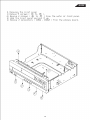
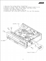
DISASSEMBLY PROCEDURE……………..….12
GENERAL UNIT EXPLODED VIEW I, II .….. ..17
CIRCUIT DESCRIPTION……….. ... ……........ 23
BASIC TROUBLESHOOTING………………… 30
DETAILED TROUBLESHOOTING …………….31
SEMICONDUCTOR IDENTIFICATION..……... 37
ELECTRICAL PARTS LIST .......…………….... 68
MECHANICAL PARTS LIST .......…..……….... 80
PRINTED ClRCUlT BOARDS .....……… …..... 83
SCHEMATIC DIAGRAMS..................….…...... 92
PACKAGE …………………………………..……95
harman/kardon, Inc.
250 Crossways Park Dr.
Woodbury, New York 11797
Rev0 11/2000
LASER BEAM SAFETY PRECAUTIONS
CLASS 1 LASER PRODUCT
CAUTION
Invisible laser radiation when the unit is open.
Do not stare into beam.
CAUTION: USE OF ANY CONTROLS, ADJUSTMENT, OR
PROCEDURES OTHER THAN THOSE SPECIFIED HEREIN
MAY RESULT IN HAZARDOUS RADIATION EXPOSURE.
Do not look directly at the laser beam
coming from the pickup or allow it to
strike against your skin.
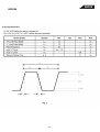
This compact disc player uses a pickup that emits a laser beam. The laser beam is emitted from the
location shown in the figure. When checking the laser diode, be sure to keep your eyes at least 1 foot away
from the pickup lens when the diode is turned on. Do not look directly at the laser beam.
CAUTION:
Using controls and adjustment, or doing procedures other than those specified herein, may result in
hazardous radiation exposure.
2
SAFETY PRECAUTIONS
This symbol is intended to alert the user to
the presence of uninsulated "dangerous
voltage" within the product's enclosure that
may be of sufficient magnitude to constitute a risk of electric shock to persons.
This symbol is intended to alert the user to
the presence of important operating and
maintenance (servicing) instructions in the
literature accompanying the appliance.
Caution:
To prevent electric shock do not use this
(polarized) plug with an extension cord, receptacle or other outlet unless the blades can be
fully inserted to prevent blade exposure.
Attention: Pour prevenir les chocs electriques ne pas
utiliser cetre fiche polarisee avec un
prolongateur, une prise de courant ou une autre sortie de courant, sauf si les lames prevent
etre inserees a fond-sans en laisser aucune
partie a decouvert.
WARNING
To prevent fire or shock hazard, do not
expose the unit to rain or moisture.
HANDLING LASER PICKUP
The laser diode in the optical system of this player can be damaged by electrostatic discharge from
your clothes or your body. Proper electrostatic grounding for service personal is required during servicing.
BEFORE REPAIRING THE COMPACT DISC PLAYER
Preparation
Human Body Grounding:
Many of the components used in this compact disc player, including the laser pickup, are sensitive to
electrostatic discharge. Service personal should be grounded with an electrostatic armband (1 Mohm).
Caution:
Static charge on clothing does not escape through a body grounding wrist band.
Be careful not to contact the pickup or electrical components with your clothing.
Workbench and Tool Grounding:
A properly-grounded electroconductive plate (1Mohm) or metal sheet should be fitted to the workbench
surface. Tools and instruments (such as soldering irons and scopes) should be grounded to prevent AC
leakage.
Note: Laser diodes are so susceptible to damage from static electricity that, even if a static discharge does
not ruin a diode, it can shorten its life or cause it to work improperly.
3
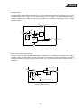
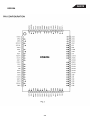
FL8370
+0!
7
0
!"#$%&"
'&()'*()
,,--*
/
0
!
/2304.
67869&&369&&3
69*369&&
+869**&3:6*&
'3;1
<(++
&
#0!
,
=+
<
(++
''!
+
, .
&/
1
*
/
5
<
>()?@(++A
<
>()?@(++A
5
/
()C>()
2(+>()?@>()
A
2(+>()?@
A
2(+()C>()?@>()
A
49>()?';
!0
+/!
0
>()?@>()
A
0
?
+
;
0@&>()3*>()A
,
B;?
D
D
;
=?
=&?
&?
B;&?
B;&?
B;?
B;?
B&;&?
&D
D
&D
=?
=?
?
B;&?
B;&?
!"#$%
7-(
0
<
>()?
5
/
@C>()A
2(+C>()?@>()
A
4
&;
B;?
D
B;;
B;?
D
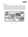
FL8370
?.+2+*
:
2+*
!
2+*
+
<7+;&
6
2+
2+
'
2
.E6+
=
&
=
,
2.
*
*
*&
=
,
2.
,
,
&
' 8
/
:8
/
8
+! 8
8
/
4"0
/'F.
∅&0
F.#
∅&0
F.
?./'F.
((;*
+6!6
#
2;$
*
1!
1
5
FL8370
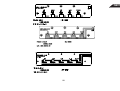
Front Panel Controls
22
21
19
17
20
18
FL 8370
15
16
13
14
12
1
2
3
Skip
Play
Pause
4
5
Disc Skip
Search
Stop
Random
Open/Close
1
Power
Phones
Phones Level
2
3
4
5
1 Power Switch: Press this switch
to apply power to the Fl8370. When
the FL 8370 is first turned on by
pressing this switch, the Status-Mode
Indicator 2 will turn green, and the
Information Display 20 will illuminate.
Press the switch again to turn the unit
off; the Status-Mode Indicator will
turn amber, indicating that the unit is
in a Standby mode. When the FL
8370 is connected to a switched AC
outlet, such as those found on the
back of many audio products, it will
return to the Standby mode when
power is applied to the switched
outlet without any further press of the
switch.
2 Status Mode Indicator: When the
Fl8370 is in the ON mode, this
indicator will glow green. When the
unit is off, the indicator will glow
amber, indicating that the unit is still
connected to the AC mains supply.
3 Headphones Jack: Connect a set
of standard headphones to this jack
for private listening.
4 Headphones Level Control: Turn
this knob to increase or decrease the
volume level for headphones
connected to the FL8370's
Headphones Jack 3 . Note that
changing this level will not change the
sound level for the unit's main output,
as that remains constant.
5 CD Drawer: This drawer holds the
discs that will be played. Press the
Open/ Close button 11 to open the
drawer so that discs may be inserted.
6 Time Button: Press this button to
select the time display. In normal
operation, this display will show the
running time of the track being played.
Press the button once to check the
time remaining for the track in play.
Press this button again to view the
total play time remaining for the disc
Time
Repeat
Intro
Clear
Program
6
7
8
9
10
in play.
7 Repeat Button: Press this button
once to constantly repeat the track
currently being played. Press it a
second time to repeat the entire disc.
8 Intro Button: Press this button to
put the Fl8370 in the Intro Scan mode.
When you press the button, the unit
will play the first 10 seconds of each
track on the disc, and then move to
the next track. Press the button again
to defeat the function and continue
full play of the current track.
9 Clear Button: Press this button to
remove tracks from a programmed
sequence. Each press of the button
will remove one track, starting with
the last track programmed to play.
10 Program Button: This button is
used to program the playback of a
disc in a particular order.
11 Open/ Close Button: Press this
button to open or close the disc
drawer. DO NOT push the drawer to
close it or damage to the transport
mechanism may result.
12 Random Button: Press this
button to put a disc into play, and to
have all of the tracks played in a
random order.
13 Pause Button: Press this button
once to momentarily pause a disc.
When the button is pressed again, the
disc will resume play at the point it
was paused.
14 Play Button: Press this button to
start the playback of a CD. If the CD
drawer is open, pressing this button
will automatically close the drawer.
15 Stop Button: Press this button to
stop the disc currently being played.
6
11
16 Skip Button: Press one side of
this button to move to the next track
or the other side of the button to
move back to the previous track
on the disc being played.
17 Search Button: Press one side of
this button to search forward
or
the other side of the button to search
backwards
through a disc to
locate a particular portion of the disc
being played.
18 Disc Skip Button: Press this
button to change to the next disc. If a
disc position is empty, the FL8370 will
automatically search for the next
position that contains a disc.
19 Disc Select Buttons: Press one
of these buttons to select the disc in a
specific position in the CD drawer.
20 Information Display: This display
provides details about the operation
of the FL 8370.
21 HDCD Indicator: This LED will
light automatically when a CD with
HDCD encoding is playing. No
further action is needed to enjoy the
benefits of HDCD.
22 Remote Sensor: The sensor
behind this window receives
commands from the remote control.
Keep this area clear if you wish to use
the FL 8370 with a remote control.
FL8370
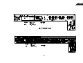
Rear Panel Connections
1
2
3
4
5
LEFT
OUT
CAUTION
RISK OF ELECTRIC SHOCK
DO NOT OPEN
IN
CLASS 1 LASER PRODUCT
RIGHT
DIGITAL
OUTPUT
REMOTE
AUDIO
OUTPUT
SHOCK HAZARD
OPEN.
SHOCK
HAZARD: DO
: DONOT
NOT
OPEN.
AVIS:RISQUE
ELECTRIQUE-NE
PASPAS
OUVRIR.
AVIS:RISQUEDE
DECHOC
CHOC
ELECTRIQUE-NE
OUVRIR.
MODEL NO: FL8370
HARMAN KARDON
NORTHRIDGE
CALIFORNIA, U.S.A.
MADE IN CHINA
SERIAL NO.
AC INPUT
AC 117V / 60Hz
20W
This device complies with part 15 of the FCC Rules.
Operation is subject to the following two conditions:
(1) This device may not cause harmful interference,
and (2) this device must accept any interference
received, including interference that may cause
undesired operation.
WARNING: "TO REDUCE THE RISK OF FIRE OR
C
ELECTRIC SHOCK, DO NOT EXPOSE THIS APPLIANCE
TO RAIN OR MOISTURE."
US
LR46800
CAN/CSA-C22.2 No.1-96
UL 1270
HDCD and High Definition Compatible Digital
are registered trademarks of Pacific Microsonics, Inc.
PRODUCT COMPLIES WITH DHHS
RULES 21CFR SUBCHAPTER J,
APPLICABLE AT DATE MANUFACTURED:
(YCL).
1
AC Power Cord
Connect this plug to an AC outlet. If the outlet is switch controlled, make certain that the switch is in the ON
position.
Coaxial Digital Output
2
Connect this jack to the coaxial-digital input of a digital audio/ video receiver or an external digital-to-analog
converter for direct access to the digital signals of the FL8370. DO NOT connect this jack to the standard audio
inputs of any device.
3
Remote Control Input
Connect this jack to the input of anther compatible Haman Kardon remote controlled device to have the remote
sensor on the Fl8370 provide signals to other products.
Remote Control Output
4
Connect this output of a remote infrared sensor or the remote control output of another compatible Harman Kardon
product. This will enable the remote control system to operate even when the front panel Remote Sensor 21 is
blocked. It will also allow use of the Fl8370 with optional, external control systems.
5
Fixed Audio Outputs
Connect these jacks to the analog CD audio inputs of your receiver, surround processor or preamplifier.
7
FL8370
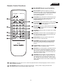
Remote Control Functions
.1
Disc Select Buttons: Press one of these buttons to
select the disc in a specific position in the CD drawer.
8
2 Numeric Buttons: Press these buttons to select a
1
1
DISC NO.
3
specific track on a disc. The FL8370 will immediately go
to the track and begin to play it. These buttons are also
used to enter track numbers into the memory for
preprogrammed-play lists.
2
4
3
5
TRACK NO.
2
1
2
3
DISC
SKIP
4
5
6
REPEAT
7
8
9
INTRO
0
CLEAR
PROGRAM
TIME
4 Search Buttons: Press these buttons to search forward
or backwards
through a disc to locate a particular
portion of the selection being played.
10
13
5
12
SEARCH
RANDOM
being played.
10
7
9
8
SKIP
7
5
Skip Buttons: Press one of these buttons to move to the
next track
, or to move back to the previous track
on the disc being played.
6 Stop Button: Press this button to stop the disc currently
11
3
4
14
Clear Button: Press this button to remove tracks from a
programmed sequence. Each press of the button will
remove one track, starting with the last track
programmed to play.
Play Button: Press this button to start the playback of a
CD. If the CD drawer is open, pressing this button will
automatically close the drawer.
8 Random Button: Press this button to play all of the
6
tracks on a disc in a random order.
9 Pause Button: Press this button once to momentarily
pause a disc. When the button is pressed again, the
disc will resume play from the point at which it was
paused.
FL 8370
10 Program Button: This button is used to program the
playback of a disc in a particular order.
11 Time Button: In normal operation, the display will show
the running time of the track being played. Press the
button once to check the time remaining for the track in
play. Press the button again to view the total play time
remaining for the disc in play.
12 Intro Button: Press this button to put the FL8370 into
the Intro Scan mode. When you press this button, the
unit will play the first 10 seconds of each track on the
disc, and then move to the next track. Press the button
again to defeat the function and continue full play of the
current track.
13 Repeat Button: Press this button once to continuously repeat the track currently being played. Press it a second
time to repeat the entire disc.
14
Disc Skip Button: Press this button to change to the next disc. If a disc position is empty, the FL8370 will
automatically search for the next position that contains a disc.
8
4
FL8370
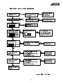
Audio Characteristics Test Procedure
Test Equipment
1. 3346 CD Player Evaluating Filter x 2 (NF Electronic Instrument)
2. VP7722 Panasonic Audio Analyzer
3. Sony YEDS18 Test CD disc
Procedure
Equipment Setup
1. The audio output of the CD player under test is connected to the CD filter L
& R inputs.
2. The outputs from the filter are connected to the Audio Analyzer.
Check the output Voltage
1. Set the mode of the filter to ‘ THRU’
2. Set the mode of Audio Analyzer to ‘ LEVEL’ mode
3. Select track 2 of the test disc and play the CD disc
4. The output voltage and gain of the R & L channels are taken by pressing
the respective buttons on the control board of Audio Analyzer.
Frequency Response
1. Set the mode of the filter to reference level mode.
2. Select the track 3, 4, 5, and 6 of the test disc and run it under ‘ Play’ mode.
3. Check the output of the R & L Channels
Total Harmonic Distortion
1. Set the mode of the filter to ‘ DIST/CH-SP’ mode
2. Set the audio analyzer to ‘ DIST’ mode.
3. Set the unit of the audio analyzer to ‘ %’ mode
4. Select the track 2, 4, and 5 on the test disc and run them under ‘ PLAY’
mode
5. Check the % of each R & L channels
9
FL8370
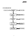
Signal to Noise Ratio
1. Set the mode of the filter to ‘ S/N’ mode
2.
3.
4.
5.
6.
Play track 2 of the test disc
The unit of the audio analyzer is set to dB mode
Press the S/N key on the control panel of the audio analyzer
Play track 7
Measure the data of S/N ratio
Dynamic Range
1. Set the mode of the filter to ‘ D-Range’ mode
2.
3.
4.
5.
Set the audio analyzer to ‘ DIST’ Mode
Set the unit of the audio analyzer to ‘ dB’ mode
Play track 17of the test disc
The dynamic range should be |A| + 60dB
Channel Separation
1. Set the mode of the filter to ‘ DIST/CH-SP’ mode
2. Set the audio analyzer to ‘ LEVEL’ mode
3. Play the tracks 8, 9, 10 & 11
4. The measured results is the difference between L & R channel
De-emphasis
1. Press the ‘ THRU’ button of the CD filter
2. Play the track 2 of the test disc
3. Press the ‘ Relative Level’ and make it ‘ ON’
4. Select the track 12 and 13 and measure the L & R channels value
10
FL8370
70
FL8370
11
FL8370
12
FL8370
13
FL8370
14
FL8370
15
FL8370
16
FL8370
17
FL8370
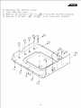
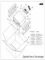
Model : FL8370 Exploded drawing List
''
/
/''
//
//
/
/
''
/
/
/
/
/
/
/
9600-505009-001
/
''
/
!"# $
($"(! ) ((*
% +) %)!,
-() .
-+,%,$!"
.) !",(0123
4(, 1/
4(, 1
56(1
56(1/
.7
. + 8
#-# $($"(! -($*($"(! .(!
7# ((*
.$*
.9:$(
8
#
#
!"%
+
!"4 966 ((*
6(,#
561
4(, 1''88
(; 8
1((*
1!,(8
!"%
%# % ) %$"(! %! )1'%:<0$!"3
18
%&
! *$! ( !
%&
%&
%$!"
%$!"
%$!"
%$!"
FL8370
&
/
/
/
/
%!
%!
%!
%!
)1':<
)1':<
)1':<=
)1':<
19
FL8370
20
FL8370
Model : 5CD Exploded drawing List
3009-110000-000
$
$
+
+
+
$$+
$
+
+
+
$$
$
$
$
+
+
("$5<
+
+
+
+
+
$
+
+
+
+
$
++
!"#
%&'!'
%&'!'('&
!)%*
))',
-.)//
!))',
0
12/"34567
14&..)8%
"%9'!:
12)
)!'
%99&//
;,*0
..)8%
.)*)*<
;*'0
!%''3))
!%''3
')).)*&
!%''3
%)''
!%''3!'
))
12/!"!-56
12/!"!567
09")4
!09")4
,9
12/1"!!56
!,9
-//,,
12/!"34-567
..)
14&..)
%)&
%)*&'
21
$
FL8370
$
96)'*
Model : 5CD Exploded drawing List
$
$
$$
$
$
$+
$
$
$
+
$
+
+
+
+
+
+$
+
+
++
+
+++
+
+
+
+
$
+
+
$
+
+
((16$$
$$
%)$*&03
%&!%''3
%&&
!.)
9")4
"%9'
12/!"!-56
-//
)''
!)''
!)''.)
)''
1))*3
-//,,%
14&0'),
14&0')
12/!"34-567
0'),
0')
12/-56!"!
1="")''
>?5$!)''
-%
..)""
14&..)
96)'*
1=%&
!%''3)3
0)3
0-),
1=/$,,
')3
12/56 '#
))!%''3
))((16$$
))
1=0)3
22
+
FL8370
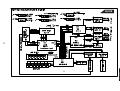
FUNCTION DESCRIPTION
1.RF Amp Block
1.1 RF Amplifier
The optical currents inputted through pins PD1(A+C) and PD2(B+D) are converted into voltages through
I-V amp, and they are added to RF summing amp. The voltage, converted from the photo diode
(A+B+C+D) signal, is outputted through RFO(pin74) and the eye pattern can be checked at this pin.
58K
PD1
-
65
VA
+
10K
-
I-V amp(1)
VC
+
VC
RFO
74
RF summing amp
58K
PD2
-
66
VB
+
RF-
10K
73
I-V amp(2)
VC
Figure 4. RF amp circuit
1.2 Focus Error Amp
The output of the focus error amp is the difference between I-V amp(1) output VA and
RF I-V amp(2) output VB. The focus error bias voltage applied to the (+) of focus error amp can be
changed by output voltage of D/A converter as shown in diagram, so that the offset of focus error amp
can be adjusted automatically by controlling 5 bits counter switches. Focus error bias can be adjusted
from the range of +100mV ~ -100mV by connecting the resistor on pin 63 (FEBIAS).
164K
32K
VB >
-
32K
VA >
sev-stopb
FEBIAS
59
+
160K
SW1
63
sev-stop
<5 Bit Counter>
4K
-
3K
X1
X2
X4
X8
X16
+
FEBIAS
vc
Figure 5. Focus error amp circuit
note1> VA and VB refer to output signal of PD1 and PD2 I/V amp.
note2> sev-stopb,sev-stop,fe-stopb and fcmpo are internal signals
23
fcmpo
+
fe-stopb
FE1
FL8370
1.3 Tracking Error Amp
The optical currents detected from the side photo diode (E and F) pf pick-up are inputted to the E and F
pin and converted into voltage signals by E I-V and F I-V amp. The output of tracking error amp
generates the difference between E I-V AMP and F I-V AMP voltage output.
The E-F balance can be adjusted by modifying the gain of E I-V AMP, and the tracking gain
can be adjusted automatically by controlling the peak voltage at pin TE2 by micom program.
TE1
LPFT
Balance
Window Comp
-
3.3K
27K
56K
BAL < 4 : 0 >
13K
79
55
53
Gain
Window Comp
1.5K
+
16K
I-V AMP
TE2
7.5K
68
13K
-
75K
EI
I-V AMP
110K
E
67
220K
F
54
To ISTAT
To ISTAT
To TRCNT
GAIN_UP/DOWN
GAIN < 3 : 0 >
Figure 6. Tracking error amp circuit
1.4 Focus OK Circuit
The FOK is the output. The focus OK circuit generates a timing window to enable focus servo operation
from focus search status. When the difference of the RFO (pin74)signal and DC coupled signal
IRF(pin75) are above the predefined voltage the Focus OK circuit output (pin40) becomes active(High
output). The predefined voltage is -0.39V
40K
RFO
74
IRF
75
40K
40K
-
57K
-
+
90K
+
VC+0.625V
Figure 7. Focus OK circuit
24
FOK
40
FL8370
1.5 Mirror Circuit
IRF signal is amplified by the mirror amp, and the peak and bottom component of amplified signal are
detected by peak and bottom hold circuit. The peak hold circuit covers traverse signal of up to 100KHz
component and bottom hold circuit capable of covering the envelope frequency of disc rotation. The time
constant for the mirror hold must be sufficiently larger than that of the traverse signal.
-
38K
IRF
75
17K
2.5K
-
Peak and
Bottom
Hold
+
19K
1.5K
1
MCP
39
MIRROR
+
17K
+
96K
+
-
Figure 8. Mirror Circuit
1.6 EFM Comparator
The EFM comparator converts a RF signal into a binary signal.
Beacuse the asymmetry generated due to variations in disc manufacturing can not be eliminated by the
AC coupling alone, this circuit uses to control reference voltage of EFM comparator for eliminating
asymmetry.
40K
RFI
77
+
100K
+
19K
+
20K
-
100K
85K
Figure 9. EFM Comparator & asymmetry circuit
25
1
EFM
39
ASY
FL8370
1.7 Defect Circuit
The RFO signal bottom, after being inverted, is held with two time constants of long and short.
The short time-constant bottom hold is done for a disc mirror defect more than 0.1msec, the long timeconstant bottom hold is done with the mirror level prior to the defect. By differentiating this with a
capacitor coupling and shifting the level, both signals are compared to generate the mirror defect
detection signal.
DCC1
5
4
DCC2
75K
RFO
75
37.5K
28K
-
BOTTOM
+
HOLD
75K
BOTTOM
VC+0.6254V
DCB
-
43K
HOLD
DFCT
41
SSTOP/DFCT
+
2
Figure 10. Defect Circuit
1.8 APC (Auto Power Control) Circuit
The laser diode has large negative temperature characteristic in its optical output when driven with a
constant current on laser diode. Therefore, the output on processing monitor photo diode, must be a
controlled current for getting regular output power, thus the APC (Auto Power Control) circuit is
composed.
PN (From micom command)
PD 69
150K
+
43.5K
-
150K
300K
150K
1.25V
+
5.5K
LDON (From micom command)
Figure 11. APC Circuit
26
0.75K
70
LD
FL8370
2.Servo Block
2.1 Focus Servo Block
When defect is "H"(the defect signal is detected), the focus servo loop is muting in case of focus phase
compensation. At this time, the focus error signal is outputted through the low pass filter formed by
connecting a capacitor(0.1uF) and a built-in 470KΩ resistor to the FDFCT pin(pin 60). Accordingly, the
focus error output is held at the error value just before defect error during defect occurring. The peak
frequency of focus loop phase compensation is at about 1.2KHz when the resistor connected to FSET
pin(pin 6) is 510KΩ, and it is inversely proportional to the resistor connected to the FSET pin. While the
focus search is operating, the FS4 switch is on and then the focus error signal is isolated, accordingly the
focus search signal is outputted by FEO pin(pin 48). When the FS2 switch is on(focus on), the focus
servo loop is on and the focus error signal from FE2 pin(pin 58) is outputted through the focus servo loop.
3.6K
60K
VC
-
FZCI
48
+
58
20K
60
FS4B
FS2B
130K
X4
92K
Focus Phase
Compensation
48K
470K
FDFCT
FSCMPO
-
+
FE2
+
X3
X2
X1
-
+
40K
47
DFCTI
FS3
10K
470K
FGD
28
27
50K
40K
580K
FS1
+
FS3
26
3
6
FLB
FSET
Figure 15. Focus servo block
27
PS
3.6K
46K
FEO
FRCH
4
3
X1
0
0
X2
0
1
X3
1
0
X4
1
1
FE-
FL8370
2.2 Tracking Servo Block
During detection of defect, the tracking error signal is outputted through the tracking servo loop after
passing the low pass filter formed by connecting a capacitor(0.1uF) and a built-in 470KΩ resistor to the
TDFCT pin(pin57) in case of tracking phase compensation. The value of tracking gain up/down can be
controlled by TGU and TG2 pin. The peak frequency of tracking loop phase compensation, the dynamic
range and offset of opamp can be adjusted by changing the value of resistor connected to FSET pin
same as focus loop. In case of unstable status of actuator after jumping, the ON/OFF of tracking loop is
controlled by TM7 switch of break circuit.
After 10-track jumping, servo circuit gets out of the liner range and actuator's tracking becomes
occasionally unstable. Hence unnecessary jumping with many tracking error should be prevented.
TM4
TE2
53
470K
680K
57
TDFCT
DFCTI
680K
TG1
10K
49
TM3
TE-
TG1
66PF
TM1
TGU
61
20K
TG2
110K
TRACKING
PHASE
COMPENSATION
82K
10K
90K
TM7
62
TG2
470K
6
FSET
Figure 16. Tracking servo block
28
+
50
TEO
FL8370
2.3 Sled Servo Block
The moving of pick-up is controlled by tracking servo output through a low pass filter.
The sled kick voltage is outputted for track jump operation.
43
TM6
TM7
PS
4
3
X1
0
0
X2
0
1
X3
1
0
X4
1
1
-
44
+
42
SLO
SLSL+
TM2
Figure 17. Sled servo block
2.4 Spindle Servo Block
The 20KΩ resistor and 0.33uF capacitor form the 200Hz low pass filter, and the carrier component of
spindle servo error signals is eliminated. In CLV-S mode, SMEF becomes "L" and pin 25 low pass filter fc
lowers, strengthening the filter further. The characteristics of high frequency phase compensation in
focus tracking servo and the characteristics of cut off frequency in CLV low pass filter are tested by FSET
pin.
SMON 24
22K
22K
220K
15K
SMDP
23
220K
20K
220K
15K
-
100K
+
50K
-
220K
25
+
Double
speed
6
SMEF
FSET
Figure 18. Spindle servo block
29
46
SPDLO
45 SPDL-
FL8370
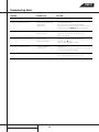
Troubleshooting Guide
SYMPTOM
POSSIBLE CAUSE
SOLUTION
No lights on front panel
• No AC power
• Make certain that the AC power cord is plugged into a live outlet
Remote does not appear to operate
• Main Power Switch turned off
• Weak batteries
• Blocked sensor
• Turn on Main Power Switch
• Install fresh batteries, observing polarity indications
• Remove obstructions from the front-panel sensor, or connect
a remote sensor to the Remote-In jack on the rear panel
Front panel lights but CD does not play
• Disc upside down
• Moisture inside unit
• Turn CD over so that label side faces up
• Leave the unit turned ON for 30 minutes to allow
moisture to evaporate
Play indicator lights but no sound is heard
• Poor connections
• Wrong source selected
• Make certain connections are secure and made to
the correct (e.g., CD) input
• Select CD source on receiver or preamp
Sound skips or stutters during play
• Disc may be damaged
• Surface vibrations
• Try another disc
• Isolate the unit from vibration by placing it on a firm surface
or move it further away from speakers
Sound is continually distorted
• Incorrect input
• Make certain that the FL 8370 is connected to a line-level
audio input, NOT a digital audio or phono input
30
FL8370
31
FL8370
32
FL8370
33
FL8370
34
FL8370
35
FL8370
36
FL8370
KB9223
RF AMP & SERVO SIGNAL PROCESSOR
OVERVIEW
80-QFP-1420C
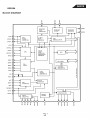
The KB9223 is a 1-chip BICMOS integrated circuit to perform the function of RF amp and servo signal processor for
compact disc player applications.It consist of blocks for RF
signal processing ,focus, tracking, sled and spindle
servo.Also this IC has adjustment free function and embedded opamp for audio post filter.
FEATURES
• RF amplifier & RF equalizer
ORDERING INFORMATION
• Focus error amplifier & servo control
• Tracking error amplifier & servo control
Device
• Mirror & defect detector circuit
KB9223
• Focus OK detector circuit
KB9223-L
Package
Tempe. Range
80-QFP-1420C
-20°C ~ +70°C
• APC(Auto Laser Power Control) circuit for constant laser
APPLICATIONS
power
• FE bias & focus servo offset adjustment free
• CD Player
• EF balance & tracking error gain adjustment free
• Video-CD
• Embedded audio post filter
RELATED PRODUCT
• The circuit for Interruption countermeasure
• KS9286 Data Processor
• Double speed play available
• KS9284 Data Processor
• Operating voltage range
• KA9258D/KA9259D Motor Driver
KB9223 : 5V
KB9223-L : 3.4V
M/M-97-P006
1997. 10. 17
37
FL8370
KB9223
E
68
EI
79
PD
69
LD
70
VR
71
78
EQO
76
IRF
75
ASY
32
EFM
33
RFI
77
DCB
2
4
FGD
FS3
58
26
28
27
3
Focus Phase
Compensation
Micom Data
Interface Logic
RF Amp
FE2
52
FLB
TZC
MLT
TE1
51
& Offset cancel circuit
Focus Error Amp
FE-BIAS Adjustment
Tracking Phase
Compensation Block
& Jump Pulse GEN.
Tracking Error Amp
E/F Balance & Gain
Control
MICOM TO SERVO CONTROL
AUTO SEQUENCER
APC Amp
LDON
ADJUSTMENT-FREE CONTROL
Center Voltage Amp.
RF Level AGC
Equalizer
Sled Servo Amplifier
& Sled Kick GEN.
FS1~
FS4
TM1~ BAL1~ PS1~
TM6 BAL5 PS4
GA1~
GA5
Spindle Servo LPF
( Double Speed )
EFM
Comparator
Mirror Detection
Circuit
Built-in Post Filter Amp ( L&R )
Defect Detection
Circuit
5
15
16
13
14
FOK Detection
Circuit
19
17
12
11
9
10
GC2I
67
35
GC2O
F
36
CH2I
63
37
CH2O
66
38
RRC
PD2
31
CH1I
65
29
MUTEI
PD1
30
CH1O
74
22
GC1I
RFO
54
GC1O
73
59
DCC1
RF-
FE1
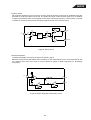
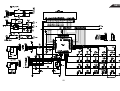
BLOCK DIAGRAM
Figure 1. Block diagram
M/M-97-P006
1997. 10. 17
38
60
FDFCT
47
FE-
48
FEO
57
TDFCT
49
TE-
50
TEO
53
TE2
55
LPFT
62
TG2
61
TGU
43
SLO
44
SL-
42
SL+
46
SPDLO
45
SPDL-
23
SMDP
24
SMON
25
SMEF
6
FSET
39
MIRROR
1
MCP
40
FOK
FL8370
KB9223
PIN CONFIGURATION
66 PD2
SSTOP
SL+
SLO
SL-
SPDL-
SPDLO
FE-
FEO
TE-
TEO
TZC
ATSC
TE2
TE1
LPFT
DVDD
TDFCT
FE2
FE1
TGU
TG2
FDFCT
65 PD1
FEBIAS
DVEE
64 63 62 61 60 59 58 57 56 55 54 53 52 51 50 49 48 47 46 45 44 43 42 41
FOK 40
MIRROR 39
67 F
RESET 38
68 E
MLT 37
69 PD
MDATA 36
70 LD
MCK 35
71 VR
VSSA 34
72 VCC
EFM 33
KB9223
73 RF-
ASY 32
74 RFO
ISTAT 31
75 IRF
TRCNT 30
76 EQO
LOCK 29
77 RFI
FGD 28
78 EQC
FS3 27
79 EI
FLB 26
SMON
SMDP
WDCK
VREG
ISET
MUTEI
9
VSSP
8
RRC
GC2I
7
GC1I
VCCP
6
GC1O
VDDA
5
CH1I
FSET
4
CH1O
DCC1
3
CH2O
DCC2
2
CH2I
FRSH
1
GC2O
DCB
SMEF 25
MCP
80 GND
10 11 12 13 14 15 16 17 18 19 20 21 22 23 24
Figure 2. Pin configuration
M/M-97-P006
1997. 10. 17
39
FL8370
KB9223
PIN DESCRIPTION
Table 1. PIN DESCRIPTION
Pin No.
Symbol
Description
1
MCP
Capacitor connection pin for mirror hold
2
DCB
Capacitor connection pin for defect Bottom hold
3
FRSH
Capacitor connection pin for time constant to generate focus search waveform
4
DCC2
The input pin through capacitor of defect bottom hold output
5
DCC1
The output pin of defect bottom hold
6
FSET
The peak frequency setting pin for focus,tracking servo and cut off frequency of CLV
LPF
7
VDDA
Analog VCC for servo part
8
VCCP
VCC for post filter
9
GC2I
Amplifier negative input pin for gain and low pass filtering of DAC output CH2
10
GC2O
Amplifier output pin for gain and low pass filtering of DAC output CH2
11
CH2I
The input pin for post filter channel2
12
CH2O
The output pin for post filter channel2
13
CH1O
The output pin for post filter channel1
14
CH1I
The input pin for post filter channel1
15
GC1O
Amplifier output pin for gain and low pass filtering of DAC output CH1
16
GC1I
Amplifier negative input pin for gain and low pass filtering of DAC output CH1
17
RRC
The pin for noise reduction of post filter bias
18
VSSP
VSS for post filter
19
MUTEI
The input pin for post filter muting control
20
ISET
21
VREG
The output pin of regulator
22
WDCK
The clock input pin for auto sequence
23
SMDP
The input pin of CLV control output pin SMDP of DSP
24
SMON
The input pin for spindle servo ON through SMON of DSP
25
SMEF
The input pin of provide for an external LPF time constant
26
FLB
The input pin for current setting of focus search,track jump and sled kick voltage
Capacitor connection pin to perform rising low bandwidth of focus loop
M/M-97-P006
1997. 10. 17
40
FL8370
KB9223
Table 1. PIN DESCRIPTION (Continued)
Pin No.
Symbol
Description
27
FS3
The pin for high frequency gain change of focus loop with internal FS3 switch
28
FGD
Reducing high frequency gain with capacitor between FS3 pin
29
LOCK
Sled runaway prevention pin
30
TRCNT
Track count output pin
31
ISTAT
Internal status output pin
32
ASY
The input pin for asymmetry control
33
EFM
EFM comparator output pin
34
VSSA
Analog VSS for servo part
35
MCK
Micom clock input pin
36
MDATA
Micom data input pin
37
MLT
38
RESET
39
MIRROR
40
FOK
The output pin of focus OK comparator
61
TGU
The capacitor connection pin for high frequency tracking gain switch
62
TG2
The pin for high frequency gain change of tracking servo loop with internal TG2 switch
63
FEBIAS
64
DVEE
65
PD1
The negative input pin of RF I/V amplifier1(A+C signal)
66
PD2
The negative input pin of RF I/V amplifier2(B+D signal)
67
F
The negative input pin of F I/V amplifier (F signal)
68
E
The negative input pin of E I/V amplifier(E signal)
69
PD
The input pin for APC
70
LD
The output pin for APC
71
VR
The output pin of (AVEE+AVCC)/2 voltage
72
VCC
VCC for RF part
73
RF-
RF summing amplifier inverting input pin
74
RFO
RF summing amplifier output pin
Micom data latch input pin
Reset input pin
The mirror output for test
Focus error bias voltage control pin
The DVEE pin for logic circuit
M/M-97-P006
1997. 10. 17
41
FL8370
KB9223
Table 1. PIN DESCRIPTION (Continued)
Pin No.
Symbol
Description
75
IRF
76
EQO
77
RFI
Tne input pin for EFM comparision
78
EQC
The capacitor connection pin for AGC
79
EI
80
GND
The input pin for AGC
The output pin for AGC
Feedback input pin of E I/V amplifier for EF Balance control
GND for RF part
M/M-97-P006
1997. 10. 17
42
FL8370
KB9223
ABSOLUTE MAXIMUM RATINGS
Table 2. Absolute Maximum Ratings
Characteristic
Symbol
Value
Unit
Vmax
6
V
PD
200
mW
Operating Temperature
TOPR
-20 ~ +70
o
C
Storage temperature
TSTG
-55 ~ +150
o
C
Supply Voltage
Power Dissipation
ELECTRICAL CHARACTERISTICS
Table 3. Electrical Characteristics
(Ta=25°C, VDD = DVDD = VCC = +5V, VSS = DVSS = GND = VSSP = 0V )
Characteristic
Symbol
Supply Current High
ICCHI
Supply Current Typ
Test Conditions
Output
Min
Typ
Max
Unit
VCC=6V,No load
-
20
40
60
mA
ICCTY
VCC=5V,No Load
-
12
30
48
mA
Supply Current Low
ICCLO
VCC=3.4V,No Load
-
10
25
40
mA
RF Amp Offset Voltage
Vrfo
input open
pin 74
-80
0
+80
mV
RF Amp Voltage Gain
Grf
SG3 f=10KHz,40mVp-p,sine
pin 74
25.1
28.1
31.1
dB
RF THD
Grfmd
SG3 f=1KHz,40mVp-p,sine
pin 74
-
-
5
%
RF Amp Max. Output Voltage
Vrfpp1
SG3 DC 2.7V
pin 74
3.8
-
-
V
RF Amp Min. Output Voltage
Vrfpp2
SG3 DC 2.3V
pin 74
-
-
1.2
V
Focus Error Amp Offset Voltage
Vfeo1
input open
pin 59
-450
-250
-50
mV
Focus Error Amp Auto Offset
Voltage
Vfeo2
WDCH=88.2KHz Pulse ,$841
pin 59
-35
0
35
mV
Focus Error Amp PD1 Voltage Gain
Gfe1
SG3 f=10KHz,32mVp-p,sine
pin 59
27
30
33
dB
Focus Error Amp PD2 Voltage Gain
Gfe2
SG3 f=10KHz,32mVp-p,sine
pin 59
27
30
33
dB
Focus Error Amp Voltage Difference
Gfe∆
∆Gfe1-∆Gfe1
pin 59
-3
0
+3
dB
Focus Error Amp Max. Output
Voltage
Gfepp1
SG3 DC 2.7V
pin 59
4.4
-
-
V
Focus Error Amp Min. Output Voltage
Gfepp2
SG3 DC2.3V
pin 59
-
-
0.6
V
AGC Max Gain
Gagc
SG4 f=500KHz,20mVp-p,sine
pin 76
16
19
22
dB
AGC EQ Gain
Geq
Gain Difference of Gagc at
f=1.5MHz
pin 76
0
1
2
dB
AGC Gain2
Gagc2
SG4 f=500KHz,0.5Vp-p,sine
pin 76
3.5
6
9
dB
AGC Cpmpress Ratio
Cagc
Gain Difference of Gagc2 at
0.1Vp-p
pin 76
0
2.5
5
dB
AGC Frequency
Fagc
Gain Difference
SG4 f=1.5MHz,0.1Vp-p,sine
and f=500KHz,0.1Vp-p,sine
pin 76
-1.5
0
2.5
dB
M/M-97-P006
1997. 10. 17
43
FL8370
KS9284
M/M-97-P006
1997. 10. 17
44
FL8370
KS9284
M/M-97-P006
1997. 10. 17
45
FL8370
KS9284
M/M-97-P006
46
FL8370
KS9284
47
FL8370
KS9284
48
FL8370
KS9284
49
FL8370
KS9284
50
FL8370
KS9284
51
FL8370
KA9258D
52
FL8370
KA9258D
53
KA9258D
FL8370
54
FL8370
®
49%
FPO
®
®
PCM1732
For most current data sheet and other product
information, visit www.burr-brown.com
24-Bit, 96kHz, Stereo Audio
DIGITAL-TO-ANALOG CONVERTER
With HDCD® Decoder
TM
FEATURES
●
●
PCM1732 uses a newly-developed “enhanced, multilevel delta-sigma modulator” architecture that improves audio dynamic performance and reduces jitter
sensitivity.
The internal digital filter operates at 8x oversampling
at a 96kHz sampling rate, with –120dB stopband
attenuation.
PCM1732
HDCD
Amplitude
Decoding
HDCD
Hidden
Code
Recovery
Low-Pass
Filter
DAC
HDCD
8x
Oversampling
Digital Filter
ML/I2S
Enhanced
Multi-Level
∆Σ
Modulator
MC/DEM
Low-Pass
Filter
DAC
MD/FSS
NOTE: An HDCD license from Pacific Microsonics, Inc. is
required to purchase the PCM1732.
VCC2R
AGND2R
●
The PCM1732 is designed for mid- to high-grade
digital audio applications which achieve 96kHz sampling rates with 24-bit audio data, such as High Definition Compatible Digital (HDCD) CD players, DVD
players, mini-disc players and AV receivers.
VCC2L
●
●
ENHANCED MULTI-LEVEL ∆Σ DAC
INPUT AUDIO DATA WORD: 16-, 20-, 24-Bit
SAMPLING FREQUENCY (fs): 16kHz - 96kHz
SYSTEM CLOCK: 256, 384, 512, 768fS
HIGH PERFORMANCE:
THD+N: –96dB
Dynamic Range: 104dB
SNR: 104dB
AUDIO OUTPUT LEVEL: 0.57 x VCC (Vp-p)
8x OVERSAMPLING DIGITAL FILTER WITH
HDCD DECODER:
Stopband Attenuation: –120dB
Passband Ripple: ±0.00001dB
HDCD Filter Optimized for 44.1kHz to 48kHz
and 88.2kHz to 96kHz
MULTI-FUNCTIONS:
Digital De-emphasis
Soft Mute
BCKIN
Serial
Digital Attenuation
Input
LRCIN
I/F
Zero Detect
DIN
Digital Gain Scaling
Reversible Output Phase
+5V SINGLE-SUPPLY OPERATION
SMALL SO-28 PACKAGE
AGND2L
●
●
●
●
●
DESCRIPTION
Mode
Control
I/F
CS/IWO
MODE
MUTE
SCK
Power-On Reset
HDCD® is a registered trademark of Pacific Microsonics, Inc.
Crystal/OSC
Open
Drain
XTI
XTO
Power Supply
CLKO
VCC1 AGND1
VDD
DGND
International Airport Industrial Park • Mailing Address: PO Box 11400, Tucson, AZ 85734 • Street Address: 6730 S. Tucson Blvd., Tucson, AZ 85706 • Tel: (520) 746-1111
Twx: 910-952-1111 • Internet: http://www.burr-brown.com/ • Cable: BBRCORP • Telex: 066-6491 • FAX: (520) 889-1510 • Immediate Product Info: (800) 548-6132
© 1999 Burr-Brown Corporation
55
EXTL
VOUTR
EXTR
ZERO
BPZ Control
RST
HDCD® technology is provided under license from Pacific Microsonics
Inc. The PCM1732’s design is covered by the following patents:
In the USA: 45,479,168, 5,638,074, 5,640,161, 5,808,574, 5,838,274
5,854,600, 5,864,311, 5,872,531.
In Australia: 669,114.
Other patents pending.
VOUTL
FL8370
SPECIFICATIONS
24-Bit Data Performance
All specifications at +25°C, +VCC = +VDD = +5V, fS = 44.1kHz, and SYSCLK = 384fS, unless otherwise noted.
PCM1732
PARAMETER
CONDITIONS
MIN
TYP
MAX
RESOLUTION
24
DATA FORMAT
Audio Data Interface Format
Data Bit Length
Audio Data Format
Sampling Frequency (fS)
System Clock Frequency(1)
System Clock Duty Cycle
Standard/I2S
16/20/24 Selectable
MSB-First, Binary Two’s Complement
16
96
256/384/512/768fS
40
60
DIGITAL INPUT/OUTPUT LOGIC LEVEL
Input Logic Level (except XTI): VIH
VIL
Output Logic Level (CLKO):
VOH
VOL
CLKO PERFORMANCE(2)
Output Rise Time
Output Fall Time
Output Duty Cycle
DYNAMIC PERFORMANCE(3, 4)
THD+N
VO = 0dB
VO = –60dB
Dynamic Range
Signal-to-Noise Ratio(5)
Channel Separation
DC ACCURACY
Gain Error
Gain Mismatch Channel-to-Channel
Bipolar Zero Error
ANALOG OUTPUT
Output Voltage(6)
Center Voltage
Load Impedance
DIGITAL FILTER PERFORMANCE
Filter Characteristics 1
(fS = 44.1kHz/48kHz optimal)
Passband
Stopband
Passband Ripple
Stopband Attenuation
Delay Time
Filter Characteristics 2
(fS = 88.2kHz/96kHz optimal)
Passband
Stopband
Passband Ripple
Stopband Attenuation
Delay Time
De-Emphasis Error
INTERNAL ANALOG FILTER
–3dB Bandwidth
Passband Response
POWER SUPPLY REQUIREMENTS
Voltage Range
Supply Current: ICC + IDD
Power Dissipation
Bits
2.0
0.8
IOH = 2mA
IOL = 4mA
4.5
0.5
20 ~ 80% VDD, 10pF
80 ~ 20% VDD, 10pF
10pF Load
5.5
4
30
fS = 44.1kHz
fS = 96kHz
fS = 44.1kHz
–96
–94
–42
f S = 44.1kHz, EIAJ A-weighted
fS = 96kHz, A-weighted
f S = 44.1kHz, EIAJ A-weighted
fS = 96kHz, A-weighted
fS = 44.1kHz
fS = 96kHz
98
98
96
Full Scale (0dB)
–90
±3.0
±3.0
±60
V
V
V
V
dB
dB
dB
% of FSR
% of FSR
mV
Vp-p
V
kΩ
5
±0.002dB
–3dB
%
dB
dB
dB
dB
dB
dB
0.57 VCC
0.5 VCC
AC Load
kHz
ns
ns
%
104
103
104
103
104
101
±1.0
±1.0
±30
VO = 0.5VCC at Bipolar Zero
UNITS
0.471fS
0.487fS
0.515fS
< 0.453fS
Stopband = 0.515fS
Stopband = 0.520fS
±0.0001
–109
–123
81/fS
±0.005dB
–3dB
dB
dB
dB
sec
0.395fS
0.441fS
0.538fS
< 0.341fS
Stopband = 0.538fS
±0.0001
–132
31/fS
±0.1
100
–0.16
f = 20kHz
VDD, VCC
fS = 44.1kHz
fS = 96kHz
fS = 44.1kHz
fS = 96kHz
4.5
TEMPERATURE RANGE
Operating
Storage
Thermal Resistance, θJA
5
35
93
425
465
–25
–55
kHz
dB
5.5
105
525
+70
+100
67
dB
dB
sec
dB
VDC
mA
mA
mW
mW
°C
°C
°C/W
NOTES: (1) Refer to the System Clock section of this data sheet. (2) An external buffer is recommended. (3) Dynamic performance specifications are tested with 20kHz low-pass
filter and THD+N specifications are tested with 30kHz LPF, 400Hz HPF, Average Mode. (4) Dynamic performance specifications are tested with HDCD gain scaling set to analog
gain scaling. (5) SNR is tested with infinite zero detection off. (6) Output level is for sine wave. DAC outputs 0.64 VCC (peak-to-peak) due to filter response as transient.
®
PCM1732
56
FL8370
SPECIFICATIONS
16-Bit Data Performance
All specifications at +25°C, +VDD = +VCC = +5V, fS = 44.1kHz, and SYSCLK = 384fS, unless otherwise noted. For discussion of HDCD scaling options, see the
Applications Considerations section of this data sheet.
PCM1732U
PARAMETER
DYNAMIC ANALOG PERFORMANCE,
STANDARD CD, ANALOG HDCD SCALING(1)
Total Harmonic Distortion + Noise
VO = 0dB
VO = –60dB
Dynamic Range
Output Voltage, Sine Wave
DYNAMIC ANALOG PERFORMANCE,
HDCD CD, ANALOG HDCD SCALING(3)
Total Harmonic Distortion + Noise
VO = 0dB
VO = –60dB
Dynamic Range
Output Voltage, Sine Wave
DYNAMIC ANALOG PERFORMANCE,
Standard CD, Digital HDCD SCALING(1)
Total Harmonic Distortion + Noise
VO = 0dB
VO = –60dB
Dynamic Range
Output Voltage, Sine Wave
DYNAMIC ANALOG PERFORMANCE
HDCD CD, Digital HDCD SCALING(2)
Total Harmonic Distortion + Noise
VO = 0dB
VO = –60dB
Dynamic Range
Output Voltage, Sine Wave
CONDITIONS
0dBFS
EIAJ A-Weighted
0dBFS(2)
0dBFS
EIAJ A-Weighted(4)
0dBFS, Without Peak Extend(2)
0dBFS, With Peak Extend(5)
+6dBFS(5, 6)
0dBFS
EIAJ A-Weighted
0dBFS
0dBFS
EIAJ A-Weighted(4)
0dBFS
+6dBFS(5)
MIN
TYP
MAX
UNITS
–95
–37
99
0.57VCC
dB
dB
dB
Vp-p
–94
–38
104
0.57VCC
0.285VCC
0.57VCC
dB
dB
dB
Vp-p
Vp-p
Vp-p
–92
–33
96
0.285VCC
dB
dB
dB
Vp-p
–91
–34
104
0.285VCC
0.57VCC
dB
dB
dB
Vp-p
Vp-p
NOTES: (1) Without dither. (2) Gain pin is LOW. (3) With the rectangular PDF dither. (4) Including Peak Extend to +6dBFS. (5) Gain pin is HIGH. (6) +6dBFS is
the full Peak Extend, while dynamic range numbers are with Peak Extend.
57
PCM1732
FL8370
PIN CONFIGURATION
PIN ASSIGNMENTS
Top View
SO-28
LRCIN
1
28
ML/I2S
DIN
2
27
MC/DEEM
BCKIN
3
26
MD/FSS
CLKO
4
25
MUTE
XTI
5
24
MODE
XTO
6
23
CS/IWO
DGND
7
22
RST
PCM1732U
VDD
8
21
ZERO
HDCD
9
20
GAIN
VCC2R 10
19
VCC2L
AGND2R 11
18
AGND2L
EXTR 12
17
EXTL
VOUTR 13
16
VOUTL
AGND1 14
15
VCC1
PIN
NAME
I/O
DESCRIPTION
1
LRCIN
IN
Left and Right Clock Input. This clock is equal to
the sampling rate, fS.(1)
2
DIN
IN
Serial Audio Data Input(1)
3
BCKIN
IN
4
CLKO
OUT
5
XTI
IN
6
XTO
OUT
7
DGND
—
Digital Ground
Digital Power +5V
Oscillator Input/External Clock Input(2)
Oscillator Output
8
VDD
—
9
HDCD
OUT
10
VCC2R
—
11
AGND2R
—
Analog Ground, Rch
12
EXTR
—
Common Mode Voltage for Analog Output Amp,
Rch
13
VOUTR
OUT
14
AGND1
—
Analog Ground
15
VCC1
—
Analog Power +5V
16
VOUTL
OUT
17
EXTL
—
18
AGND2L
OUT
19
VCC2L
—
20
GAIN
OUT
21
ZERO
OUT
22
RST
IN
Reset. When this pin is LOW, the digital filter
and modulators are held in reset.(3)
23
CS/IW0
IN
Chip Select/Input Format Selection. When this
pin is LOW, the Mode Control interface is enabled.(4)
24
MODE
IN
Mode Control Select: H = Software; L =
Hardware(3)
25
MUTE
IN
Mute Control(3)
26
MD/FSS
IN
Mode Data/Sampling Rate Range Select(3)
27
MC/DEM
IN
Mode Clock/De-Emphasis Select(3)
28
ML/I2S
IN
Mode Latch/Input Format Select(3)
ABSOLUTE MAXIMUM RATINGS
Power Supply Voltage ...................................................................... +6.5V
+VCC to +VDD Difference ................................................................... ±0.1V
Input Logic Voltage .................................................. –0.3V to (VDD + 0.3V)
Input Current (except power supply) ............................................... ±10mA
Power Dissipation .......................................................................... 750mW
Operating Temperature Range ......................................... –25°C to +70°C
Storage Temperature ...................................................... –55°C to +125°C
Lead Temperature (soldering, 5s) ................................................. +260°C
(reflow, 10s) .................................................... +235°C
Bit Clock Input for Serial Audio Data(1)
Buffered System Clock Output.
HDCD Encoded Data Detect
Analog Power +5V, Rch
Analog Voltage Output, Rch
Analog Voltage Output, Lch
Common Mode Voltage for Analog Output Amp,
Lch
Analog Ground, Lch
Analog Power +5V, Lch
External (analog) Gain Scaling
Zero Data Flag
NOTES: (1) Schmitt Trigger input. (2) CMOS logic level input. (3) Schmitt
Trigger input with pull-up resister. (4) Schmitt Trigger input with pull-down
resistor.
PACKAGE/ORDERING INFORMATION
PRODUCT
PACKAGE
PACKAGE
DRAWING
NUMBER(1)
PCM1732U
SO-28
217
–25°C to +70°C
PCM1732U
"
"
"
"
"
SPECIFIED
TEMPERATURE
RANGE
PACKAGE
MARKING
ORDERING
NUMBER(2)
TRANSPORT
MEDIA
PCM1732U
PCM1732U/1K
Rails
Tape and Reel
NOTES: (1) For detailed drawing and dimension table, please see end of data sheet, or Appendix C of Burr-Brown IC Data Book. (2) Models with a slash (/) are
available only in Tape and Reel in the quantities indicated (e.g., /1K indicates 1000 devices per reel). Ordering 1000 pieces of “PCM1732U/1K” will get a single
1000-piece Tape and Reel. For detailed Tape and Reel mechanical information, refer to Appendix B of Burr-Brown IC Data Book.
ELECTROSTATIC
DISCHARGE SENSITIVITY
This integrated circuit can be damaged by ESD. Burr-Brown
recommends that all integrated circuits be handled with
appropriate precautions. Failure to observe proper handling
and installation procedures can cause damage.
ESD damage can range from subtle performance degradation
to complete device failure. Precision integrated circuits may
be more susceptible to damage because very small parametric
changes could cause the device not to meet its published
specifications.
®
PCM1732
58
FL8370
Motor driver ICs
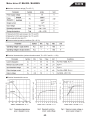
Reversible motor driver
BA6209 / BA6209N
The BA6209 and BA6209N are reversible-motor drivers suitable for brush motors. Two logic inputs allow three output
modes : forward, reverse, and braking. The motor revolving speed can be set arbitrarily by controlling the voltage applied
to the motor with the control pin voltage VR.
Applications
VCRs and cassette tape recorders
Features
1) Power transistors can handle a large current
(1.6A maximally).
2) Brake is applied when stopping the motor.
3) Built-in function to absorb rush currents generated by
reversing and braking.
4) Motor speed controlling pin.
5) Small standby current.
(VCC = 12V, IO = 5.5mA typically)
6) Stable operation during mode changes either from
forward to reverse or vice versa.
7) Interface with CMOS devices.
Block diagram
59
FL8370
Motor driver IC BA6209 / BA6209N
FAbsolute maximum ratings (Ta = 25_C)
FRecommended operating conditions (Ta = 25_C)
FElectrical characteristics (unless otherwise noted, Ta = 25_C and VCC = 12V)
FElectrical characteristic curves
60
FL8370
Motor driver IC BA6209 / BA6209N
61
FL8370
Motor driver IC BA6209 / BA6209N
Measurement circuit
62
FL8370
Motor driver IC BA6209 / BA6209N
Circuit operation
Input / output truth table
(3) Rush current absorption circuit
When a high voltage (caused by such as a motor reversal) is generated on OUT1 and OUT2, an internal
comparator detects the high voltage and turns on an internal circuit that absorbs rush currents.
(4) Drive circuit
The forward direction of the motor connected between
OUT1 and OUT2 corresponds to the current flow from
OUT1 to OUT2, and the reverse direction corresponds to
the current flow from OUT2 to OUT1. The output voltage
(VOUT) applied to the motor is given by the equation :
VOUT (V) = VZD VCE (sat.) = VZD 0.2 (IOUT = 100mA)
where VZD is the zener voltage of the constant voltage
diode (ZD) connected to pin 4.
If Vref is left OPEN, the output voltage (VOUT) is given by
the equation :
VOUT (V) = VCC1 VCE (sat.) (PNP) 2VF VCE (sat.)
= VCC1 1.8 (IOUT = 100mA)
Forward / reverse control, forced stop, and rush current
absorption are controlled by the combination of FIN and
RIN input states.
(1) Forward / reverse control circuit
When FIN is HIGH and RIN is LOW, current flows from
OUT1 to OUT2. When FIN is LOW and RIN is HIGH, current flows from OUT2 to OUT1 (refer to the truth table).
(2) Forced stop circuit
By setting RIN and FIN both HIGH or both LOW, power
supply to the motor is shut down and a brake is applied
by absorbing the motor counter-electromotive force.
Pin descriptions
63
FL8370
MCU Pin Arrangement and Functions
VCC
POWER
37
33
P77
38
P73
DSNS
39
34
TRSW
40
P75
RL+
41
MUTE
RL42
35
HDCD
43
36
DAC.CLK
DAC.LAT
46
44
DAC.DATA
47
45
P21
P20
48
Pin Arrangement
P22
49
32
SUBQ
VFD.DO
50
31
SQCK
VFD.DI
51
30
P55
VFD.CLK
52
29
P54
VFD.LAT
53
28
XRST
P1 4
54
27
MDATA
P1 5
55
26
MLAT
TRCNT
56
25
MCLK
REMOTE
57
24
STAT
12
13
14
15
16
S2
DN
UP
S0S1
PB1/AN1
S1
P60
11
17
10
64
S0
PB2/AN2
RES
P61
9
18
OSC2
63
8
PB3/AN3
7
P62
VSS
P63
19
OSC1
20
62
6
61
PB4/AN4
X1
PB5/AN5
5
FOK
4
21
X2
60
TEST
PB6/AN6
3
LKFS
AVSS
P66
22
2
23
59
1
58
PB0/AN0
AVCC
PB7/AN7
Figure 1.2 Pin Arrangement
64
FL8370
Internal Block Diagram
Timer B1
SCI3
Port 8
SCI1
Port 7
Timer A
P77
P76/TMOV
P75/TMCIV
P74/TMRIV
P73
Port 6
P30/SCK1
P31/SI1
P32/SO1
RAM
P67
P66
P65
P64
P63
P62
P61
P60
Port 5
Port 1
P20/SCK3
P21/RXD
P22/TXD
ROM
P87
P86/FTID
P85/FTIC
P84/FTIB
P83/FTIA
P82/FTOB
P81/FTOA
P80/FTCI
P57/INT7
P56/INT6/TMIB
P55/INT5/ADTRG
P54/INT4
P53/INT3
P52/INT2
P51/INT1
P50/INT0
Port 3
P10/TMOW
P14/PWM
P15/IRQ1
P16/IRQ2
P17/IRQ3/TRGV
Port 2
Data bus (lower)
Data bus (upper)
CPU
H8/300L
Address bus
VSS
VCC
RES
IRQ0
TEST
X1
X2
Subclock
generator
System clock
generator
OSC1
OSC2
Figure 1.1 shows a block diagram.
Timer X
Watchdog
timer
14-bit PWM
A/D converter
PB0/AN0
PB1/AN1
PB2/AN2
PB3/AN3
PB4/AN4
PB5/AN5
PB6/AN6
PB7/AN7
Port B
AVCC
AVSS
P90/FVPP*
P91
P92
P93
P94
Port 9
Timer V
Figure 1.1 Block Diagram
65
CMOS largecurrent port
IOL= 10 mA
@VOL= 1V
FL8370
Pin Functions
Pin Name
PB1
PB0
AVSS
TEST
X2
X1
VSS
OSC1
OSC2
RES
S0
S1
S2
DN
UP
S0S1
P60
P61
P62
P63
FOK
LKFS
P66
STAT
MCLK
MLAT
MDATA
XRST
P54
P55
SQCK
SUBQ
VCC
P73
MUTE
P75
POWER
P77
DSNS
TRSW
RL+
RLHDCD
DAC.LAT
DAC.CLK
DAC.DATA
P20
P21
1
2
3
4
5
6
7
8
9
10
11
12
13
14
15
16
17
18
19
20
21
22
23
24
25
26
27
28
29
30
31
32
33
34
35
36
37
38
39
40
41
42
43
44
45
46
47
48
Description
No connection
No connection
Connected 0V
Connected 0V
No connection
Connected 5V
MCU ground line; connected to 0V
10MHz crystal input
10MHz crystal input
MCU reset line; 0V = reset; 5V = normal operation
CD Changer Mechanism door position switch
CD Changer Mechanism door position switch
CD Changer Mechanism door position switch
CD Changer Mechanism door motor control line
CD Changer Mechanism door motor control line
CD DSP SUBQ ready input; high pulse for SUBQ ready
No connection
No connection
No connection
No connection
CD DSP focus OK; 5V = focus OK
CD DSP tracking lock output; 5V = servo lock
No connection
CD DSP internal status output
CD DSP serial command clock
CD DSP command latch
CD DSP serial command data
CD DSP reset line; 0V = DSP reset
No connection
No connection
SUBQ output serial clock
SUBQ output
MCU power supply; connected to 5V
No connection
System mute control; 5V = mute
No connection
Servo power on/off control; 5V = power on
No connection
Disc detection optical sensor output; 0V = disc present
Carousel position detection optical sensor output
Carousel motor line
Carousel motor line
HDCD decoding status from PCM1732; 5V = HDCD
PCM1732 serial command latch
PCM1732 serial command clock
PCM1732 serial command data
No connection
No connection
66
FL8370
49
50
51
52
53
54
55
56
57
58
59
60
61
62
63
64
P22
VFD.DO
VFD.DI
VFD.CLK
VFD.LAT
P14
P15
TRCNT
REMOTE
AVCC
PB7
PB6
PB5
PB4
PB3
PB2
No connection
Display driver status serial data
Display driver command serial data
Display driver command serial clock
Display driver command serial latch
No connection
No connection
CD DSP internal status for auto-adjustment
IR remote signal input
Connected to 5V
No connection
No connection
No connection
No connection
No connection
No connection
67
FL8370
QTY
1
2
3
13
15
4
1
2
1
1
"
1
1
4
#
3
2
1
1
2
#
2
1
1
3
#
2
1
! #
1
1
1
#
2
1
3
3
2
5
!
68
FL8370
3
2
1
1
#
1
1
#
2
2
1
#
2
1
$#$%
1
$#$%
4
$##&%
1
$##'%
26
$#(%
4
$#$%
2
$##'%
1
$#(%
1
$##(%
1
$
))$##'%
5
$
))$##'%
2
$
))$##'%
2
$
))$##'%
1
$
))$##'%
2
$
))$#$%
2
$
))$#$%
1
$
))$##'%
2
$
))$#$%
1
$
))$##'%
1
$
))$##'%
1
#$#'%
10
#$#'%
1
#$#&%
9
#$#'%
1
#$#'%
2
#$#&%
1
!
69
FL8370
#$#&%
3
$'%
2
#$#'%
1
#$#'%
2
#$#&%
3
#$##&%
1
#$#&%
1
#$#&%
8
#$##&%
1
#$##&%
2
$#$%$
1
$#$%$$
2
$*'+,
1
$)*'+,
6
-
$$)
1
$$)*'+,
1
$$
*'+,
1
.+.%'
1
.
.
.
8
.
.
6
/
/.
./
1
/
/.
.#%#
1
/
/.
.#%
3
.#�*,
1
)1$$')$
1
)#$$')$
1
+
$$ 2
! +
$$ 3
+
#$#22$
1
+
$$ 1
+
$$ 4
+
#$#$*,
1
+
$$ 1
$
+3$
1
$
$3 1
*
.,
$
+3'
70
1
FL8370
$
$
.+3$
1
$
.0+3$
1
$
.+3$
1
$
.+3$
1
$
.+3$
1
$
#+.#3
1
*.#,
$
#+.#3
1
*.#,
4
$.+3
1
*
.+.,
$
.
'$+3.
1
$
$
'$+3'.
1
.+
'$'
.*
,
1
F301
4030-160000-512
1.6A 5x20mm
1
'$
0$
2
).).%*
,
1
).).%*
,
1
$%
+
'$'.+.
1
FOR
F301
!
'
!
##$.$$$
2
!
##
.%*
,
1
!
.%
'
1
!
##$
*
,
2
!
##
1
!
##%
*+
,
1
!
##
*
,
1
!
##
* ,
1
!
##-$'+$
1
!
##.'+
.%
1
!
##-$'+.$
1
'
##.'.
1
*,
.%
71
1
FL8370
2
2
4
2
2
2
%#
"
))$
1
$#$%
2
$##'%
1
$##&%
3
#$#'%
2
#$#&%
2
#$#&%
1
+
$$ 2
!
#.$
* ),
1
+
.$.
+.+*,+3
1
1
.$
.%
1
!
1
$$*,
5
"
$
+3$
1
.%
1
$
.
+$'
1
*'+,
%'3)*
.,
1
.
500#5
1
72
FL8370
$'$'
1
"
$
+3'$
1
.
+3+
1
$
.%
1
1
1
5
1
1
$##&%
1
#$#&%
2
.
.
5
"
++
$22$
1
"
/
#$22$
1
"
$+
$)$
1
$$*,
15
'
.
$
1
!
%.+'
1
##$-$$
1
%..$)
.%
1
1
1
#
1
2
1
$#$%
3
!
73
FL8370
$#$%
2
$#(%
1
$#$%
2
#$#&%
1
$$*'+,
1
.
.
2
.
###
1
1
"
+
$$ 1
+
$$ 1
+
$$ 1
!
# )
2
!
1
$
'$%
1
##$"$%#&"$' (
1
##%
1
'$'
.%
1
!
$#$%
1
$#$%
1
$#$%
1
$#$%
1
/
#$22$
1
++
$$
1
$)$++
#$
1
+.+*,+3
$###$
1.0
.%
1.0
74
1
FL8370
1
++
$$
1
++
$$
1
## "$'##
1
## "$'## 1
1
)
! $
1
$ 1
*
1
$
)+00
1
.
$
1
*+,
$
$
1
$
1
$
%)
1
)*)!,
1
))
1
00
))
*,
1
))
1
)
1
)$
1
)+
1
)$.)
1
0$)$$
1
4
#
1
$#(%
2
#$#'%/
1
$)
2
75
FL8370
.
.4
1
5)
5
1
..)
1
##$
1
.%
1
.
2
0)$/
2
00
1
$#0#0#6
2
$)
1
'
1
4
$
1
+
1
+
1
%
###
1
'4
1
4'
1
.$+4+
1
.$+4+
1
$+%
1
.4##
5
$4
1
).$
5
'+#0#0
1
#0$##$
2
#0$)$/
1
0$##$#
5
0$##$#
1
#00#
2
)
1
'+
2
$')
)
1
+
)
1
+
1
!
76
FL8370
.#0
1
0*,
2
00#'
1
$
+3'22$
1
$')
1
*',
1
')
1
1
.4+
)
1
)
1
1
1
.$4
1
.
1
%4
.4
1
.)%
1
1
+4
$
1
1
.+
1
.+
1
%
4
'
1
%
1
.%$')
1
.%$')$
1
.
1
.'+$')
1
.'+$
1
$+%
1
.$+4%
4
'
1
+4
1
.'+$+
1
'++
1
.'
+
2
7##$#$
2
#0/
1
0$)$/
1
0$##$#
7
77
FL8370
.'%
0)$/
1
0$##$#
1
00
1
#00#
1
#00#
3
$#00#6/
2
#00/
1
00#
3
+)
1
4+4'
1
$4
1
$
$
1
.$4
1
)
1
$')
1
$').
1
.
.)%
1
+
$$ 1
%
1
$
1
'4
%
1
.
.
.)%
1
+
$$ 1
.%
*',
1
4.)%
1
)
.
1
4.
1
$4
1
$4
'.
1
'
.4..
2
'
.4.+
2
#0/
2
0$)$/
4
$'$
1
!"#$%&'#()$*&')#
1
.'
.)%
1
+
$$ 1
+
#$22$
1
$
+3$
1
78
FL8370
$#$%
3
$##&%
1
/800
2
+.+*,+3
1
.
500#5
4
.$$
1
1
'.
*9:;<=,
1
#
+3'
1
.
*%,
1
0
1
00
1
'
'
%
1
.)%.
1
)%.
1
#0%
.
1
.
1
$
'%
'4*#0#,
1
.
#.
.
1
%*&$
'%
'4*#0#,
1
7.
.7
2
'40*,
1
.
*%,
2
.
.
*%,
2
.
)$'
1
.
%
$
)+
*,
1
$
)+00*$,
1
$
)+
'*,
1
$
)+00
1
#$##$$
1
'
1
!
2
'00#0#
2
0##$#
2
79
FL8370
#00#
2
0'0#0#
1
00#
1
%'*,%
)%
1
$
*
$+,
4
$
1
.
!)
%
1
..
+
.
4.
1
.
.$)
1
*,
4.$)
1
4.$.
1
4.
1
4$
+$.
1
4$
+
1
%$.
1
4%
1
4$
$.
1
4$
1
4$
1
.
5 5
1
*!$.,
4
$
1
.
'
1
*!$.,
80
FL8370
4$)
1
.4
.
2
.4.
1
4..
1
4..
1
+4
1
4
1
.
$
1
*,
$
1
$*$
,
1
.
.
2
1
$4$.
1
$
1
.
*!
%,
1
%$
$
1
$)
1
4
$
1
4$
*,
1
.
+
.+
1
+0#
2
.$$
1
.
+
.+
1
%$
1
$+4$
1
$.
00
1
$.
4006
2
'+
2
.'$.4+
4
'00#0#
1
'00
2
0##$#*,
0$##$#
3
0##$#
1
0$##$#*,
7
0$##$#
18
0)$/
2
0
1
0$$/
2
81
37
FL8370
0
2
00
1
#00#
1
00
3
0$##$#
1
0$##$#
17
#00#
82
1
FL8370
83
FL8370
84
FL8370
85
FL8370
86
FL8370
87
FL8370
88
FL8370
89
FL8370
90
FL8370
91
FL8370
1.6A
92
FL8370
93
FL8370
94
FL8370
95
Ref# Part Number
Description
1
2
3
4
5
6
7
8
9
10
Polyfoam, FL8370
E.P.E. Sheet P-EP500160-05
Polybag For Manual
FL8370 Owner’s Manual
1M Audio Cable
Polybag For Audio Cord
FL8370 Remote Control
FL8370
Polybag 600X600X4C MM
FL8370 Outer Carton
5000-835001-001
5206-500160-050
5200-230321-030-01
1111-FL8370
2611-310009-000
5200-100180-030
9805-020000-061
FL8370BLK
5200-600600-040
5013-835001-001-05